Embed Size (px)
Citation preview
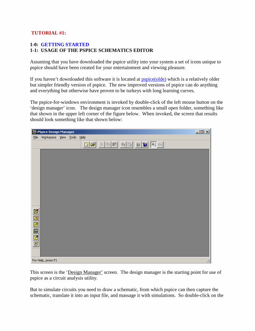
TUTORIAL #1: 1-0: GETTING STARTED 1-1: USAGE OF THE PSPICE SCHEMATICS EDITOR Assuming that you have downloaded the pspice utility into your system a set of icons unique to pspice should have been created for your entertainment and viewing pleasure. If you haven’t downloaded this software it is located at pspice(olde) which is a relatively older but simpler friendly version of pspice. The new improved versions of pspice can do anything and everything but otherwise have proven to be turkeys with long learning curves. The pspice-for-windows environment is invoked by double-click of the left mouse button on the ‘design manager’ icon. The design manager icon resembles a small open folder, something like that shown in the upper left corner of the figure below. When invoked, the screen that results should look something like that shown below:
This screen is the ‘Design Manager’ screen. The design manager is the starting point for use of pspice as a circuit analysis utility. But to simulate circuits you need to draw a schematic, from which pspice can then capture the schematic, translate it into an input file, and massage it with simulations. So double-click on the
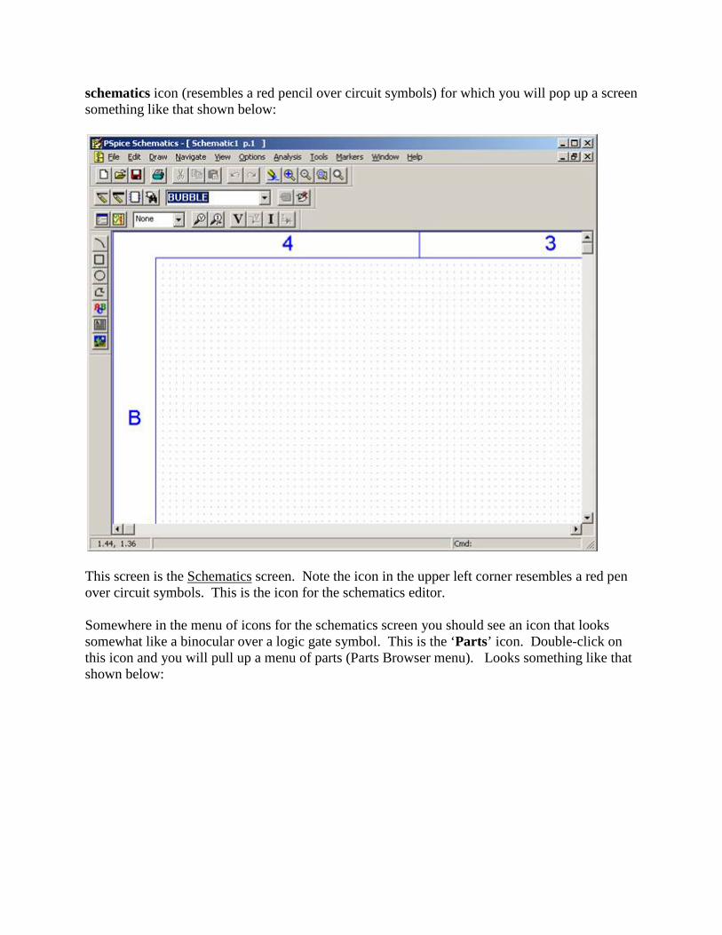
schematics icon (resembles a red pencil over circuit symbols) for which you will pop up a screen something like that shown below:
This screen is the Schematics screen. Note the icon in the upper left corner resembles a red pen over circuit symbols. This is the icon for the schematics editor. Somewhere in the menu of icons for the schematics screen you should see an icon that looks somewhat like a binocular over a logic gate symbol. This is the ‘Parts’ icon. Double-click on this icon and you will pull up a menu of parts (Parts Browser menu). Looks something like that shown below:
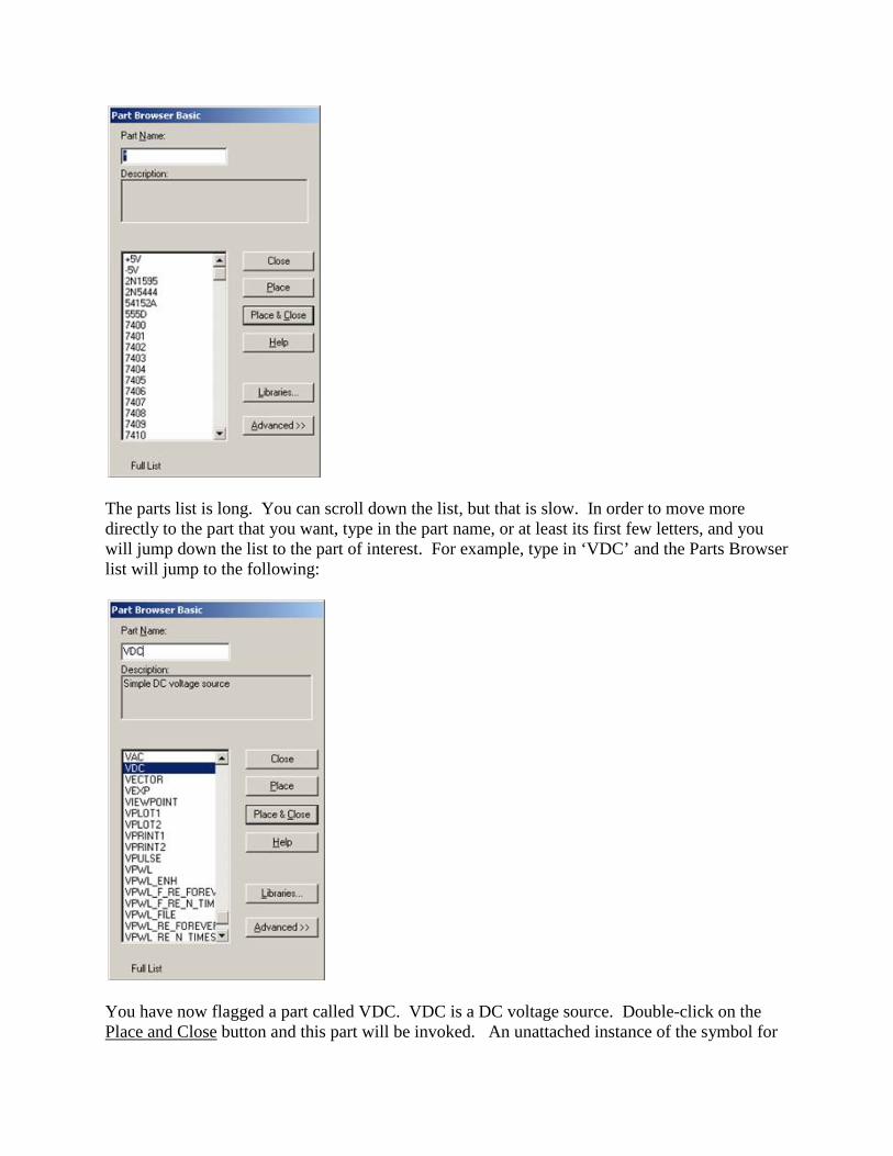
The parts list is long. You can scroll down the list, but that is slow. In order to move more directly to the part that you want, type in the part name, or at least its first few letters, and you will jump down the list to the part of interest. For example, type in ‘VDC’ and the Parts Browser list will jump to the following:
You have now flagged a part called VDC. VDC is a DC voltage source. Double-click on the Place and Close button and this part will be invoked. An unattached instance of the symbol for
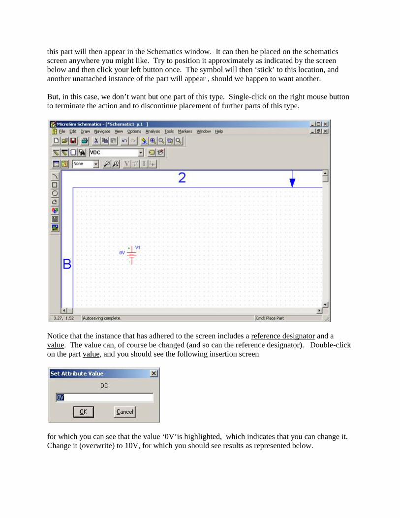
this part will then appear in the Schematics window. It can then be placed on the schematics screen anywhere you might like. Try to position it approximately as indicated by the screen below and then click your left button once. The symbol will then ‘stick’ to this location, and another unattached instance of the part will appear , should we happen to want another. But, in this case, we don’t want but one part of this type. Single-click on the right mouse button to terminate the action and to discontinue placement of further parts of this type.
Notice that the instance that has adhered to the screen includes a reference designator and a value. The value can, of course be changed (and so can the reference designator). Double-click on the part value, and you should see the following insertion screen
for which you can see that the value ‘0V’is highlighted, which indicates that you can change it. Change it (overwrite) to 10V, for which you should see results as represented below.
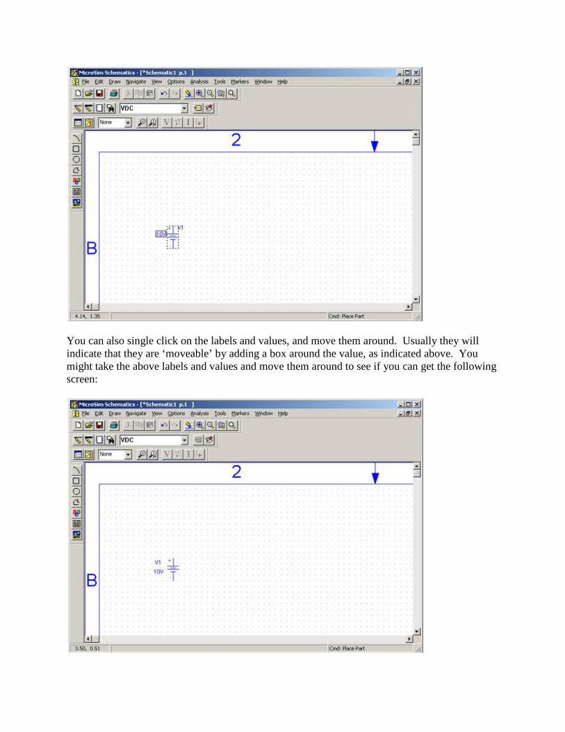
You can also single click on the labels and values, and move them around. Usually they will indicate that they are ‘moveable’ by adding a box around the value, as indicated above. You might take the above labels and values and move them around to see if you can get the following screen:
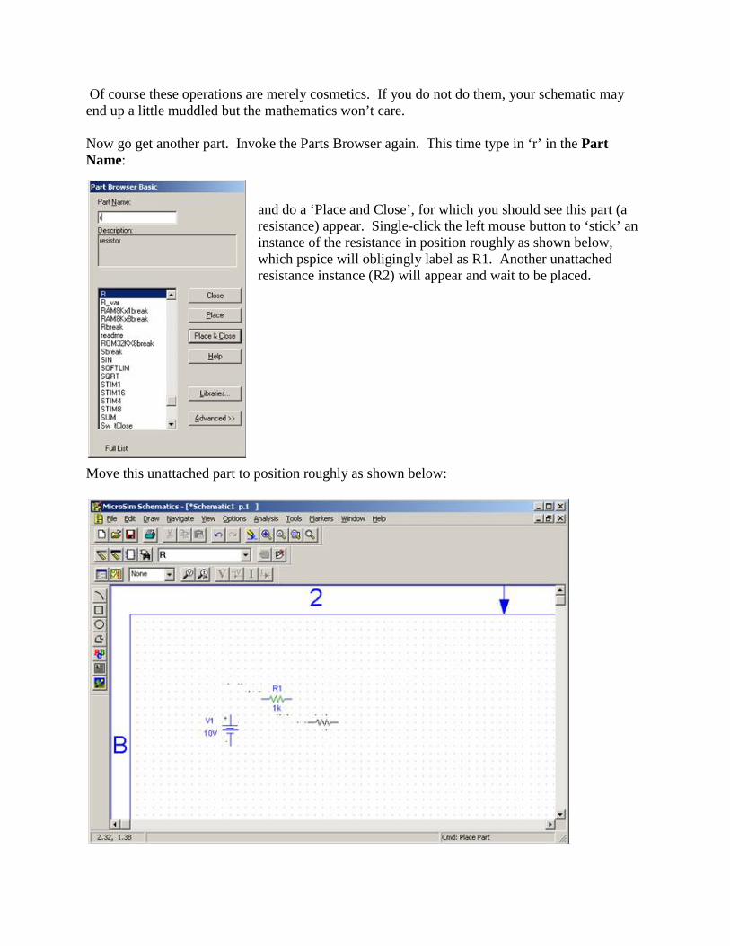
Of course these operations are merely cosmetics. If you do not do them, your schematic may end up a little muddled but the mathematics won’t care. Now go get another part. Invoke the Parts Browser again. This time type in ‘r’ in the Part Name:
and do a ‘Place and Close’, for which you should see this part (a resistance) appear. Single-click the left mouse button to ‘stick’ an instance of the resistance in position roughly as shown below, which pspice will obligingly label as R1. Another unattached resistance instance (R2) will appear and wait to be placed.
Move this unattached part to position roughly as shown below:
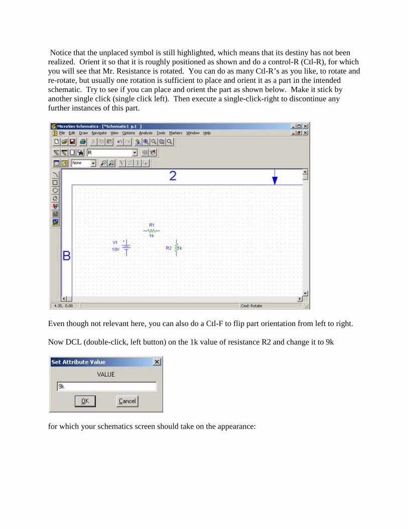
Notice that the unplaced symbol is still highlighted, which means that its destiny has not been realized. Orient it so that it is roughly positioned as shown and do a control-R (Ctl-R), for which you will see that Mr. Resistance is rotated. You can do as many Ctl-R’s as you like, to rotate and re-rotate, but usually one rotation is sufficient to place and orient it as a part in the intended schematic. Try to see if you can place and orient the part as shown below. Make it stick by another single click (single click left). Then execute a single-click-right to discontinue any further instances of this part.
Even though not relevant here, you can also do a Ctl-F to flip part orientation from left to right. Now DCL (double-click, left button) on the 1k value of resistance R2 and change it to 9k
for which your schematics screen should take on the appearance:
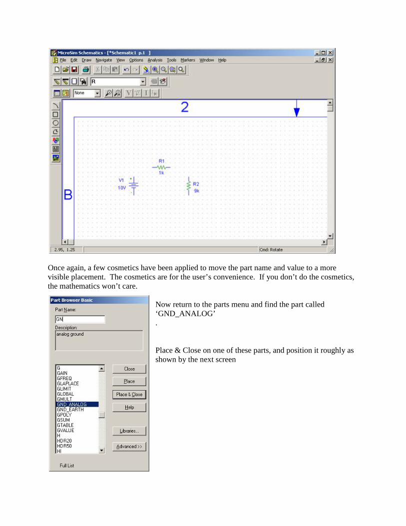
Once again, a few cosmetics have been applied to move the part name and value to a more visible placement. The cosmetics are for the user’s convenience. If you don’t do the cosmetics, the mathematics won’t care.
Now return to the parts menu and find the part called ‘GND_ANALOG’ . Place & Close on one of these parts, and position it roughly as shown by the next screen
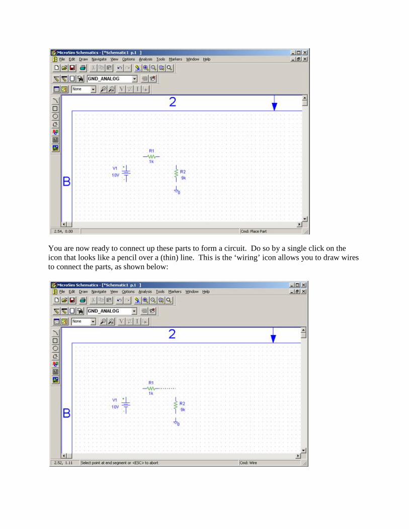
You are now ready to connect up these parts to form a circuit. Do so by a single click on the icon that looks like a pencil over a (thin) line. This is the ‘wiring’ icon allows you to draw wires to connect the parts, as shown below:
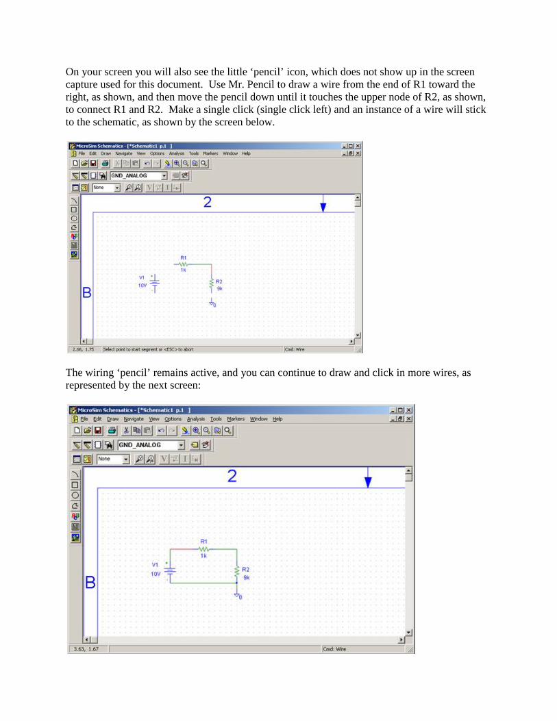
On your screen you will also see the little ‘pencil’ icon, which does not show up in the screen capture used for this document. Use Mr. Pencil to draw a wire from the end of R1 toward the right, as shown, and then move the pencil down until it touches the upper node of R2, as shown, to connect R1 and R2. Make a single click (single click left) and an instance of a wire will stick to the schematic, as shown by the screen below.
The wiring ‘pencil’ remains active, and you can continue to draw and click in more wires, as represented by the next screen:
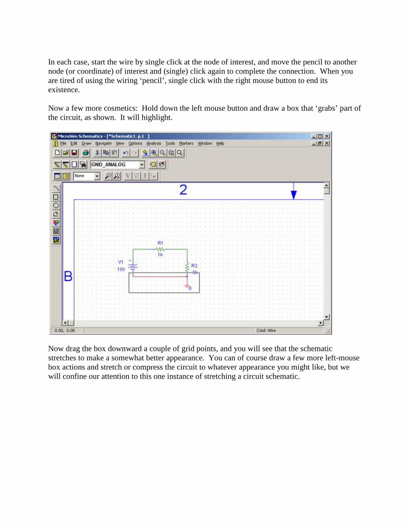
In each case, start the wire by single click at the node of interest, and move the pencil to another node (or coordinate) of interest and (single) click again to complete the connection. When you are tired of using the wiring ‘pencil’, single click with the right mouse button to end its existence. Now a few more cosmetics: Hold down the left mouse button and draw a box that ‘grabs’ part of the circuit, as shown. It will highlight.
Now drag the box downward a couple of grid points, and you will see that the schematic stretches to make a somewhat better appearance. You can of course draw a few more left-mouse box actions and stretch or compress the circuit to whatever appearance you might like, but we will confine our attention to this one instance of stretching a circuit schematic.
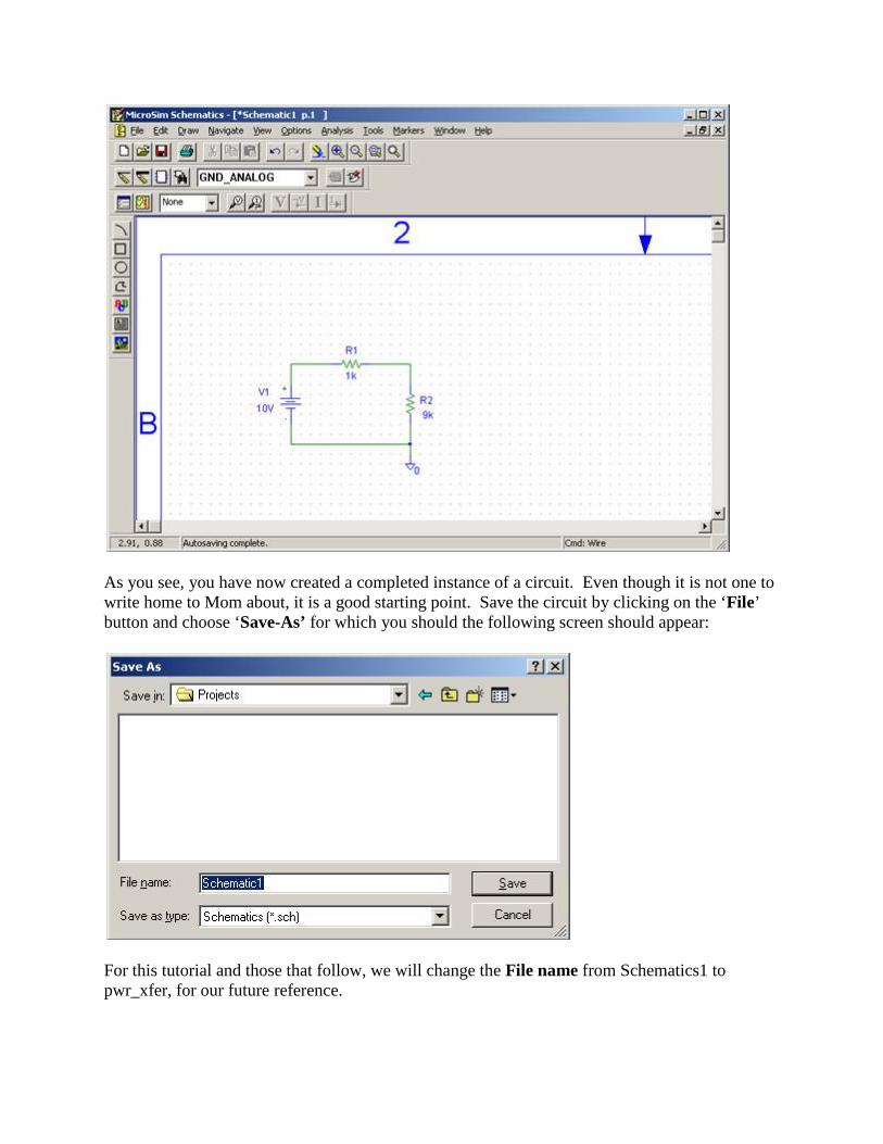
As you see, you have now created a completed instance of a circuit. Even though it is not one to write home to Mom about, it is a good starting point. Save the circuit by clicking on the ‘File’ button and choose ‘Save-As’ for which you should the following screen should appear:
For this tutorial and those that follow, we will change the File name from Schematics1 to pwr_xfer, for our future reference.
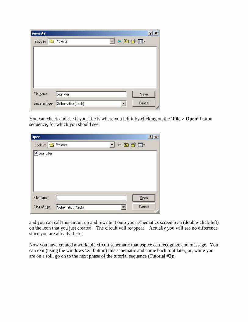
You can check and see if your file is where you left it by clicking on the ‘File > Open’ button sequence, for which you should see:
and you can call this circuit up and rewrite it onto your schematics screen by a (double-click-left) on the icon that you just created. The circuit will reappear. Actually you will see no difference since you are already there. Now you have created a workable circuit schematic that pspice can recognize and massage. You can exit (using the windows ‘X’ button) this schematic and come back to it later, or, while you are on a roll, go on to the next phase of the tutorial sequence (Tutorial #2):