Embed Size (px)
Citation preview

Appl. Phys. Lett. 118, 013106 (2021); https://doi.org/10.1063/5.0033241 118, 013106
© 2021 Author(s).
Two-dimensional van der Waals electricalcontact to monolayer MoSi2N4
Cite as: Appl. Phys. Lett. 118, 013106 (2021); https://doi.org/10.1063/5.0033241Submitted: 14 October 2020 . Accepted: 15 December 2020 . Published Online: 08 January 2021
Liemao Cao, Guanghui Zhou, Qianqian Wang, L. K. Ang, and Yee Sin Ang
COLLECTIONS
This paper was selected as an Editor’s Pick
Two-dimensional van der Waals electrical contactto monolayer MoSi2N4
Cite as: Appl. Phys. Lett. 118, 013106 (2021); doi: 10.1063/5.0033241Submitted: 14 October 2020 . Accepted: 15 December 2020 .Published Online: 8 January 2021
Liemao Cao,1,2 Guanghui Zhou,3 Qianqian Wang,2 L. K. Ang,2,a) and Yee Sin Ang2,a)
AFFILIATIONS1College of Physics and Electronic Engineering, Hengyang Normal University, Hengyang 421002, China2Science, Mathematics and Technology (SMT), Singapore University of Technology and Design (SUTD), 8 Somapah Road,Singapore 487372, Singapore
3Department of Physics, Hunan Normal University, Changsha 410081, China
a)Authors to whom correspondence should be addressed: [email protected] and [email protected]
ABSTRACT
A two-dimensional (2D) MoSi2N4 monolayer is an emerging class of air-stable 2D semiconductors possessing exceptional electrical andmechanical properties. Despite intensive recent research effort devoted to uncover the material properties of MoSi2N4, the physics of electri-cal contacts to MoSi2N4 remains largely unexplored thus far. In this work, we study van der Waals heterostructures composed of MoSi2N4
contacted by graphene and NbS2 monolayers using first-principles density functional theory calculations. We show that the MoSi2N4/NbS2contact exhibits an ultralow Schottky barrier height (SBH), which is beneficial for nanoelectronics applications. For the MoSi2N4/graphenecontact, the SBH can be modulated via the interlayer distance or via external electric fields, thus opening up an opportunity for reconfigura-ble and tunable nanoelectronic devices. Our findings provide insights into the physics of 2D electrical contacts to MoSi2N4 and shall offer acritical first step toward the design of high-performance electrical contacts to MoSi2N4-based 2D nanodevices.
Published under license by AIP Publishing. https://doi.org/10.1063/5.0033241
The discovery of monolayer graphene1 has initiated tremendousexperimental and theoretical effort for the search of new two-dimensional (2D) materials with exotic physical properties and func-tionalities. One important example is the family of 2D transition metaldichalcogenides (TMDCs), such as MoS2 and WS2, whose potential innanoelectronic,2 optoelectronic,3 photonic,4 valleytronic,5 and energydevice6 applications has revolutionized nanomaterial science andtechnology in recent years. The potential of 2D TMDCs in industrial-grade 2D nanodevices is further boosted by the enormous design flexi-bility offered by vertical van der Waals heterostructures (VDWHs) inwhich physical properties can be custom-made by vertically stackingdifferent 2D atomic layers.7–11
Beyond 2D TMDCs, ultrathin transition metal nitrides (TMNs)have been actively explored in recent years.12 As TMN is a nonlayeredmaterial, the experimental synthesis of an air-stable and large-area 2DTMN monolayer remains a formidable challenge.13–22 In 2020,MoSi2N4, a TMN-based monolayer with no known 3D parent struc-ture, has been successfully synthesized using the chemical vapor depo-sition (CVD) method,23 which represents a milestone in the searchof 2D TMN-based nanomaterial. MoSi2N4, composed of a MoN2
monolayer sandwiched by two Si–N bilayers, is an indirect bandgap
semiconductor with excellent ambient air stability. The intrinsic elec-tron and hole mobilities are predicted to be 270 cm2 V–1 s�1 and12002 V–1 s�1, respectively, which are substantially higher than that ofMoS2. Density functional theory (DFT) simulation has furtherrevealed an expansive family of MA2Z4 monolayers (M¼ early transi-tion metal, e.g., Mo, W, and Nb; A¼ Si or Ge; Z¼N, P, or As), cover-ing semiconducting, metallic, and magnetic phases. The discovery ofthe MoSi2N4 and MA2Z4 monolayer family thus opens up anuncharted territory for the exploration of 2D-material-based devicetechnology.
Although recent experiments have shed important light on thestructural, electrical, mechanical, and optical properties of MoSi2N4,
23
the physics of electrically contacting MoSi2N4 with metals26–32
remains largely unknown thus far. In 2D TMDCs, their van der Waals(VDW) stacking with 2D metals has led to myriads of unusual charac-teristics, such as weak Fermi level pinning,34 tunable bandgap,35–37
miniband formation,38 and opto-valleytronic spin injection.39 In rele-vance to MoSi2N4, the rich physical phenomena already observed in2D-TMDC/2D-metal contacts immediately lead to the following openquestions: can MoSi2N4 be integrated with 2D metals, such as gra-phene and NbS2, to form structurally stable VDWHs? What are the
Appl. Phys. Lett. 118, 013106 (2021); doi: 10.1063/5.0033241 118, 013106-1
Published under license by AIP Publishing
Applied Physics Letters ARTICLE scitation.org/journal/apl

electronic properties of such heterostructures? What types of contact,Ohmic or Schottky, are formed in such electrical contacts? Can thecontact properties and types be engineered via external tuning knobssuch as the electric field and interlayer distances?
In this work, we address the above questions by performing afirst-principles DFT simulation on the electronic properties ofMoSi2N4 when it is vertically contacted by 2D metallic electrodes—graphene and NbS2 monolayers. We find that MoSi2N4/NbS2Schottky contacts exhibit an ultralow Schottky barrier height (SBH) of0.042 eV, which is beneficial for room-temperature device operation.For MoSi2N4/graphene, the SBH can be controlled by the interlayerdistance or by the external electric field, thus allowing the contact tobe reconfigured between p-type and n-type Schottky contacts. As theextended family of MA2Z4 contains myriads of 2D monolayers withexotic physical properties yet to be unearthed, our findings shall forma harbinger for designing efficient electrical contacts and VDWHsbased on the MA2Z4 monolayer family.
The structural optimization and electronic properties of anisolated monolayer MoSi2N4 and its VDWH when interfaced withgraphene and NbS2 are studied using the Vienna simulation package(VASP).33,40 The projector-augmented wave (PAW)41 potentials areused to treat the electron-ion interaction. The generalized gradientapproximation (GGA) within Perdew–Burk–Ernzerhof (PBE) pseudo-potentials is used to describe the exchange correlation functionals. Acutoff energy of 500 eV is set. The DFT-D3 method is used to correctthe effect of weak VDW interaction.42 A vacuum layer (>20 A)between the neighboring layers is employed along the z-directionof the heterostructures to eliminate the layer interactions caused bythe neighboring slabs. The break criterion for the electronicself-consistency is set to 10–6eV. Monkhorst-Pack k-point grids of9� 9� 1 are chosen. All atoms are fully relaxed using the conjugatedgradient method until the force is lower than 0.01V/A.
The top and side views of an isolated MoSi2N4 are shown inFigs. 1(a) and 1(b), respectively. The optimized lattice constant forMoSi2N4 is a ¼ b ¼ 2:91 A, which is a hexagonal structure with aspace group of P6m1. MoSi2N4 is composed of septuple atomic layerswith a thickness of 7.01 A. Monolayer MoSi2N4 exhibits an indirectbandgap of 1.78 eV [Fig. 1(c)], compared to that of MoS2 (1.9 eV) andWS2 (2.0 eV) monolayers.58 We further note that the calculations basedon PBE functional are closer to the experimental values of 1.94 eVwhen compared to the HSE06 values of 2.29 eV23 and 2.35 eV.24
We consider the 2D/2D contacts37,43,44 formed by vertically con-tacting MoSi2N4 with graphene and NbS2, namely, MoSi2N4/grapheneand MoSi2N4/NbS2 VDWHs. We use MoSi2N4
ffiffiffi
3p�
ffiffiffi
3p
and gra-phene 2� 2 supercells to form MoSi2N4/graphene. For MoSi2N4/NbS2, MoSi2N4 2� 2 and NbS2
ffiffiffi
3p�
ffiffiffi
3p
supercells are used[Figs. 1(d)–1(g)]. To avoid the properties of MoSi2N4 being affected bymechanical stress, we fix the lattice of MoSi2N4 and apply strains ingraphene and NbS2 monolayers for MoSi2N4/graphene and MoSi2N4/NbS2, respectively. The lattice mismatch is 1.6% and 0.07% forMoSi2N4/graphene and MoSi2N4/NbS2, respectively. The stackingconfigurations have a minimal effect on the physical properties of theheterostructures (see the supplementary material). After structuralrelaxation, the interlayer distances are obtained as 3.302 A and 3.192A for MoSi2N4/graphene and MoSi2N4/NbS2, respectively, which aremuch larger than the sum of the covalent radii of N and C (S) atoms.The interfaces are found to be dominated by the VDW interactions.
We further test the interlayer distances using different VDW function-als (see the supplementary material), and the interlayer distances ofthe fully relaxed structures are found to be similar. We calculated thebinding energy Eb as Eb ¼ ðEH � EM � EgðnÞÞ=N , where EH, EM,EgðnÞ, and N denote the total energies of the heterostructures, isolatedMoSi2N4, isolated graphene (or NbS2), and the number of atoms inthe heterostructures, respectively. The calculated binding energies are�199.89 eV/atom and �280.29 eV/atom for MoSi2N4/graphene andMoSi2N4/NbS2, respectively, which are substantially lower than thoseof other 2D-material-based heterostructures.50 Coupled with the excel-lent mechanical properties of MoSi2N4,
23–25 the heterostructures arethus expected to be energetically favorable and stable.
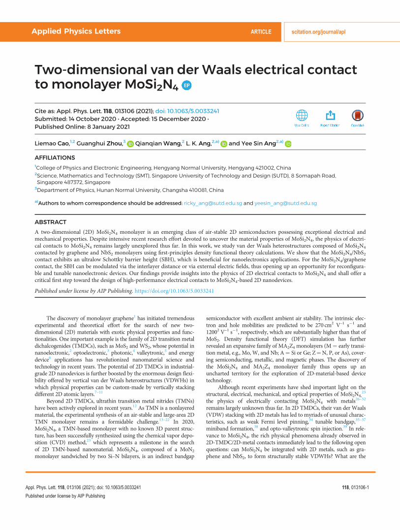
The projected band structures of MoSi2N4/graphene andMoSi2N4/NbS2 (Fig. 2) exhibit no obvious difference when SOC isincluded (see the supplementary material). The band structures ofMoSi2N4, graphene, and NbS2 are well-preserved upon forming theheterostructures. MoSi2N4 exhibits a direct bandgap in the MoSi2N4/graphene heterostructure due to band folding, which is a typicalfeature in 2D VDWHs. We determine the SBH via the Schottky-Mottrule,45 i.e., Un ¼ ECBM � EF ;Up ¼ EF � EVBM , where Un and Up are
FIG. 1. (a) and (b) Top and side views of monolayer MoSi2N4. (c) Band structure ofMoSi2N4. (d)–(g) Top and side views of optimized heterostructures of MoSi2N4/gra-phene and MoSi2N4/NbS2.
Applied Physics Letters ARTICLE scitation.org/journal/apl
Appl. Phys. Lett. 118, 013106 (2021); doi: 10.1063/5.0033241 118, 013106-2
Published under license by AIP Publishing
the interface potential barrier heights for electrons and holes, respec-tively; ECBM, EF, and EV BM are the energy of the conduction bandminimum (CBM), Fermi energy, and valence band maximum (VBM).For MoSi2N4/graphene, the n-type SBH (UnÞ and the p-type SBH(Up) are 0.922 eV and 0.797 eV, respectively, thus indicating the pres-ence of a p-type Schottky contact. In MoSi2N4/NbS2, the n-type SBH(Un) and the p-type SBH (Up) are 1.642 eV and 0.042 eV, respectively.The ultralow p-type SBH of the MoSi2N4/NbS2 contact immediatelysuggests the potential of NbS2 as an efficient 2D electrical contact toMoSi2N4 with high charge injection efficiency, particularly well-suitedfor room-temperature device applications.
We next examine the planar averaged charge density differenceand electrostatic potentials of the MoSi2N4/graphene and MoSi2N4/NbS2 heterostructures along the z direction (Fig. 3). We define theplane-averaged differential charge density (Dq) as Dq ¼ qH � qM�qgðnÞ, where qH and qM and qgðnÞ are the plane-averaged chargedensity of the heterostructures and isolate plane-averaged charge den-sities of MoSi2N4 and graphene (NbS2), respectively. The symmetry ofthe MoSi2N4 lattice structure is broken when contacted by grapheneand NbS2, thus leading to charge redistribution. Charge carriers aredepleted around the graphene layer while accumulating near theMoSi2N4 layer [Figs. 3(a) and 3(b)]. In contrast, MoSi2N4/NbS2
FIG. 2. The projected electronic band structures of (a) MoSi2N4/graphene and (b)MoSi2N4/NbS2. Here, blue and red symbols denote the contributions from MoSi2N4and graphene (NbS2), respectively.
FIG. 3. Plane-averaged differential charge density Dq, 3D isosurface of the electron density difference, electrostatic potentials, and band diagram of (a)–(d) MoSi2N4/grapheneand (e)–(h) MoSi2N4/NbS2 heterostructures, respectively.
Applied Physics Letters ARTICLE scitation.org/journal/apl
Appl. Phys. Lett. 118, 013106 (2021); doi: 10.1063/5.0033241 118, 013106-3
Published under license by AIP Publishing
exhibits excess charges accumulate around the NbS2 layer whiledepleting around the MoSi2N4 layer. Moreover, the amount of trans-ferred electrons between MoSi2N4 and NbS2 is much greater than thatbetween MoSi2N4 and graphene by direct comparison betweenFigs. 3(a) and 3(e). The 3D isosurfaces of the charge density differenceare calculated in Figs. 3(b) and 3(f) for MoSi2N4/graphene andMoSi2N4/NbS2, respectively, which clearly illustrate the differences ofcharge transfer behavior in the two heterostructures. Such charge trans-fer causes the Fermi level to move toward the valence band of MoSi2N4,resulting in an ultralow SBH. In Figs. 3(c) and 3(g), the plane-averagedelectrostatic potential difference (Veff) reveals that the direction ofthe built-in electric field is different for the two heterostructures. Thecorresponding band alignment diagrams of MoSi2N4/graphene andMoSi2N4/NbS2 are shown in Figs. 3(d) and 3(h), respectively.
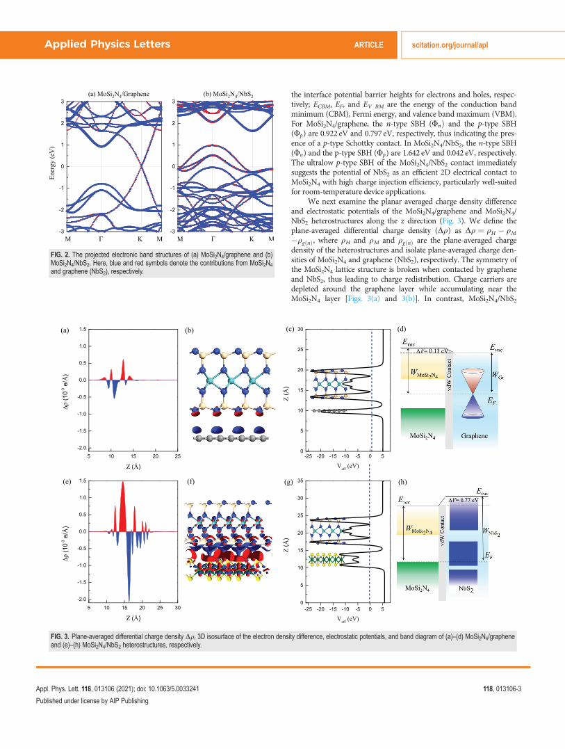
Changing the interlayer spacing, which can be achieved experi-mentally by nanomechanical pressure,46 diamond anvil cells,47
vacuum thermal annealing,48 or inserting hexagonal BN dielectriclayers,49 provides a viable route to tune the electronic properties ofVDWHs. The SBH of MoSi2N4/graphene and MoSi2N4/NbS2 as afunction of the vertical strain is illustrated in Fig. 4 (see the supple-mentary material for their band structures). Both electron and holeSBHs of the MoSi2N4/graphene heterostructure are sensitively
influenced by the interlayer distance [Fig. 4(a)]. For instance, an inter-layer larger than 3.5 A signifies the transition from a p-type Schottkycontact to an n-type Schottky contact. In contrast, the SBH of theMoSi2N4/NbS2 heterostructure remains robust against interlayerdistance variation [Fig. 4(b)].
Electrically tunable electronic properties are useful characteristicsfor the design of all-electrical devices.50–52 In Figs. 4(c) and 4(d), weexamine the evolution of the SBH as a function of an external electricfield applied along the z-direction of the heterostructures (see thesupplementary material for the band structures). We define the posi-tive direction of the electric field as that pointing from the MoSi2N4
layer to the 2D metals. For the MoSi2N4/graphene contact, when theexternal electric field is greater than 0.05V/A, the contact is trans-formed from p-type to n-type Schottky contact [Fig. 4(c)]. The appli-cation of an external electric field thus provides a tuning knob todynamically control the contact type of the MoSi2N4/graphene hetero-structure. For MoSi2N4/NbS2, the SBH is insensitive to an externalelectric field [Fig. 4(d)]. When a negative electric field exceeding�0.02V/A is applied, the p-type SBH is completely eliminated, thustransforming MoSi2N4/NbS2 into an Ohmic contact. The SBH tuningoriginates from the Fermi level shifting in graphene and NbS2. Whenthe interlayer spacing is changed or when an external electric field isapplied, the balance of the system is destroyed. To reestablish equilib-rium, the charges redistribute themselves across the interface, whichchanges the Fermi level of contacting graphene and NbS2
53,54 and,hence, their work functions. As a result, the SBH is modified.
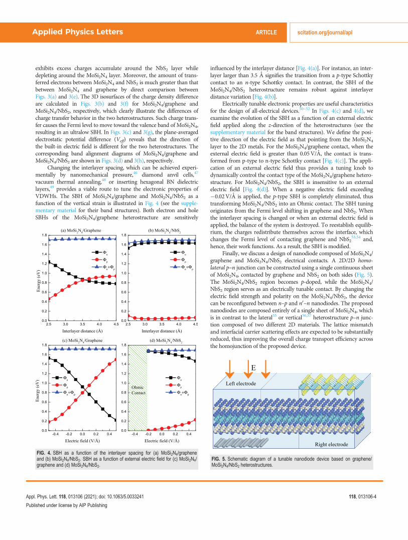
Finally, we discuss a design of nanodiode composed of MoSi2N4/graphene and MoSi2N4/NbS2 electrical contacts. A 2D/2D homo-lateral p–n junction can be constructed using a single continuous sheetof MoSi2N4, contacted by graphene and NbS2 on both sides (Fig. 5).The MoSi2N4/NbS2 region becomes p-doped, while the MoSi2N4/NbS2 region serves as an electrically tunable contact. By changing theelectric field strength and polarity on the MoSi2N4/NbS2, the devicecan be reconfigured between n–p and n0–n nanodiodes. The proposednanodiodes are composed entirely of a single sheet of MoSi2N4, whichis in contrast to the lateral55 or vertical56,57 heterostructure p–n junc-tion composed of two different 2D materials. The lattice mismatchand interfacial carrier scattering effects are expected to be substantiallyreduced, thus improving the overall charge transport efficiency acrossthe homojunction of the proposed device.
FIG. 4. SBH as a function of the interlayer spacing for (a) MoSi2N4/grapheneand (b) MoSi2N4/NbS2. SBH as a function of external electric field for (c) MoSi2N4/graphene and (d) MoSi2N4/NbS2.
FIG. 5. Schematic diagram of a tunable nanodiode device based on graphene/MoSi2N4/NbS2 heterostructures.
Applied Physics Letters ARTICLE scitation.org/journal/apl
Appl. Phys. Lett. 118, 013106 (2021); doi: 10.1063/5.0033241 118, 013106-4
Published under license by AIP Publishing

In summary, we investigated the electrical contacts betweenmonolayer MoSi2N4 with 2D semimetal (graphene) and 2D metal(NbS2) using first-principles simulation. Here, the ultralow SBH inMoSi2N4/NbS2 contact can be a particularly beneficial feature for devi-ces operating at room temperature. For the MoSi2N4/graphene con-tact, the SBH can be controlled externally via an electric field or viainterlayer distance, thus revealing potential in reconfigurable deviceapplications. Our findings shall shed important light on the design ofMoSi2N4-based 2D/2D contacts and heterostructures, thus paving acritical first-step toward the development of VDW heterostructuredevices59 based on the emerging 2D material family of MA2Z4.
See the supplementary material for the complete electronic bandstructures of MoSi2N4 heterostructures under different contact orien-tations and the evolution of the electronic band structures under dif-ferent interlayer distances and external electric fields.
This work was supported by the Singapore MOE Tier 2 (GrantNo. 2018-T2-1-007). L.C. acknowledge the support of ScienceFoundation of Hengyang Normal University of China (Grant No.18D26), the Hunan Provincial Natural Science Foundation of China(Grant No. 2019JJ50016). L.C. and G.Z. acknowledge the support ofthe National Natural Science Foundation of China (Grant No.11774085). All the calculations were carried out using thecomputational resources provided by the National SupercomputingCentre (NSCC) Singapore.
DATA AVAILABILITY
The data that support the findings of this study are availablefrom the corresponding author upon reasonable request.
REFERENCES1K. S. Novoselov, A. K. Geim, S. V. Morozov, D. Jiang, Y. Zhang, S. V. Dubonos,I. V. Grigorieva, and A. A. Firsov, Science 306, 666 (2004).
2G. Fiori, F. Bonaccorso, G. Iannaccone, T. Palacios, D. Neumaier, A. Seabaugh,S. K. Banerjee, and L. Colombo, Nat. Nanotechnol. 9, 768 (2014).
3Y.-Q. Bie, G. Grosso, M. Heuck, M. M. Furchi, Y. Cao, J. Zheng, D. Bunandar,E. Navarro-Moratalla, L. Zhou, D. K. Efetov et al., Nat. Nanotechnol. 12, 1124(2017).
4F. Xia, H. Wang, D. Xiao, M. Dubey, and A. Ramasubramaniam, Nat.Photonics 8, 899 (2014).
5Y. Ye, J. Xiao, H. Wang, Z. Ye, H. Zhu, M. Zhao, Y. Wang, J. Zhao, X. Yin, andX. Zhang, Nat. Nanotechnol. 11, 598 (2016).
6E. Pomerantseva and Y. Gogotsi, Nat. Energy 2, 17089 (2017).7A. K. Geim and I. V. Grigorieva, Nature 499, 419 (2013).8A. C. Ferrari, F. Bonaccorso, V. Fal’ko, K. S. Novoselov, S. Roche, P. Boggild, S.Borini, F. H. L. Koppens, V. Palermo, N. Pugno et al., Nanoscale 7, 4598 (2015).
9A. Bafekry, M. M. Obeid, C. V. Nguyen, M. Ghergherehchi, and M. BagheriTagani, J. Mater. Chem. A 8, 13248 (2020).
10A. Bafekry, B. Akgenc, S. F. Shayesteh, and B. Mortazavi, Appl. Surf. Sci. 505,144450 (2020).
11A. Bafekry and M. Neek-Amal, Phys. Rev. B 101, 085417 (2020).12K. Huang, Z. Li, G. Han, and P. Huang, Chem. Soc. Rev. 47, 5109 (2018).13X. Xiao, H. Wang, W. Bao, P. Urbankowski, L. Yang, Y. Yang, K. Maleski, L.Cui, S. J. L. Billinge, G. Wang et al., Adv. Mater. 31, 1902393 (2019).
14H. Liu, A. T. Neal, Z. Zhu, Z. Luo, X. Xu, D. Tom�anek, and P. D. Ye, ACSNano 8, 4033 (2014).
15Q. H. Wang, K. Kalantar-Zadeh, A. Kis, J. N. Coleman, and M. S. Strano, Nat.Nanotechnol. 7, 699 (2012).
16B. Feng, J. Zhang, Q. Zhong, W. Li, S. Li, H. Li, P. Cheng, S. Meng, L. Chen,and K. Wu, Nat. Chem. 8, 563 (2016).
17M. Naguib, V. N. Mochalin, M. W. Barsoum, and Y. Gogotsi, Adv. Mater. 26,992 (2014).
18K. Khan, A. K. Tareen, M. Aslam, R. Wang, Y. Zhang, A. Mahmood, Z.Ouyang, H. Zhang, and Z. Guo, J. Mater. Chem. C 8, 387 (2020).
19M. E. Beck and M. C. Hersam, ACS Nano 14, 6498 (2020).20L. Cao, Y. S. Ang, Q. Wu, and L. K. Ang, Phys. Rev. B 101, 035422(2020).
21J. Lipton, G.-M. Weng, J. A. R€ohr, H. Wang, and A. D. Taylor, Matter 2, 1148(2020).
22X. Li, L. Tao, Z. Chen, H. Fang, X. Li, X. Wang, J.-B. Xu, and H. Zhu, Appl.Phys. Rev. 4, 021306 (2017).
23Y.-L. Hong, Z. Liu, L. Wang, T. Zhou, W. Ma, C. Xu, S. Feng, L. Chen, M.-L.Chen, D.-M. Sun, X.-Q. Chen, H.-M. Cheng, and W. Ren, Science 369, 670(2020).
24A. Bafekry, M. Faraji, D. M. Hoat, M. M. Fadlallah, M. Shahrokhi, F. Shojaei,D. Gogova, and M. Ghergherehchi, arXiv:2009.04267v1 (2020).
25C. Yang, Z. Song, X. Sun, and J. Lu, arXiv:2010.10764 (2020).26A. Venugopal, L. Colombo, and E. M. Vogel, Appl. Phys. Lett. 96, 013512(2010).
27Y. S. Ang, H. Y. Yang, and L. K. Ang, Phys. Rev. Lett. 121, 056802 (2018).28D. S. Schulman, A. J. Arnold, and S. Das, Chem. Soc. Rev. 47, 3037 (2018).29A. Allain, J. Kang, K. Vanerjee, and A. Kis, Nat. Mater. 14, 1195 (2015).30S. Banerjee, L. Cao, Y. S. Ang, L. K. Ang, and P. Zhang, Phys. Rev. Appl. 13,064021 (2020).
31W. Xiong, C. Xia, X. Zhao, T. Wang, and Y. Jia, Carbon 109, 737 (2016).32Q. Y. Wu, Y. S. Ang, L. M. Cao, and L. K. Ang, Appl. Phys. Lett. 115, 083105(2019).
33G. Kresse and J. Furthm€uller, Phys. Rev. B 54, 11169 (1996).34Y. Liu, P. Stradins, and S.-H. Wei, Sci. Adv. 2, e1600069 (2016).35A. Ebnonnasir, B. Narayanan, S. Kodambaka, and C. V. Ciobanu, Appl. Phys.Lett. 105, 031603 (2014).
36F. Zhang, W. Li, Y. Ma, Y. Tang, and X. Dai, RSC Adv. 7, 29350 (2017).37L. Cao, Y. S. Ang, Q. Wu, and L. K. Ang, Appl. Phys. Lett. 115, 241601(2019).
38D. Pierucci, H. Henck, J. Avila, A. Balan, C. H. Naylor, G. Patriarche, Y. J.Dappe, M. G. Silly, F. Sirotti, A. T. C. Johnson et al., Nano Lett. 16, 4054(2016).
39Y. K. Luo, J. Xu, T. Zhu, G. Wu, E. J. McCormick, W. Zhan, M. R. Neupane,and R. K. Kawakami, Nano Lett. 17, 3877 (2017).
40G. Kresse and J. Furthm€uller, Comput. Mater. Sci. 6, 15 (1996).41G. Kresse and D. Joubert, Phys. Rev. B 59, 1758 (1999).42S. Grimme, J. Antony, S. Ehrlich, and H. Krieg, J. Chem. Phys. 132, 154104(2010).
43H. G. Shin, H. S. Yoon, J. S. Kim, M. Kim, J. Y. Lim, S. Yu, J. H. Park, Y. Yi, T.Kim, S. C. Jun, and S. Im, Nano Lett. 18, 1937 (2018).
44X. Ding, S. Zhang, M. Zhao, Y. Xiang, K. H. L. Zhang, X. Zu, S. Li, and L. Qiao,Phys. Rev. Appl. 12, 064061 (2019).
45J. Bardeen, Phys. Rev. 71, 717 (1947).46M. Dienwiebel, G. S. Verhoeven, N. Pradeep, J. W. M. Frenken, J. A.Heimberg, and H. W. Zandbergen, Phys. Rev. Lett. 92, 126101 (2004).
47S. Clark, K.-J. Jeon, J.-Y. Chen, and C.-S. Yoo, Solid State Commun. 154, 15(2013).
48S. Tongay, W. Fan, J. Kang, J. Park, U. Koldemir, J. Suh, D. S. Narang, K. Liu, J.Ji, J. Li, R. Sinclair, and J. Wu, Nano Lett. 14, 3185 (2014).
49H. Fang, C. Battaglia, C. Carraro, S. Nemsak, B. Ozdol, J. S. Kang, H. A.Bechtel, S. B. Desai, F. Kronast, A. A. Unal, G. Conti, C. Conlon, G. K. Palsson,M. C. Martin, A. M. Minor, C. S. Fadley, E. Yablonovitch, R. Maboudian, andA. Javey, Proc. Natl. Acad. Sci. U. S. A. 111, 6198 (2014).
50J. E. Padilha, A. Fazzio, and A. J. R. da Silva, Phys. Rev. Lett. 114, 066803(2015).
51W. Hu, T. Wang, R. Zhang, and J. Yang, J. Mater. Chem. C 4, 1776 (2016).52L. Britnell, R. V. Gorbachev, R. Jalil, B. D. Belle, F. Schedin, A. Mishchenko,T. Georgiou, M. I. Katsnelson, L. Eaves, S. V. Morozov, N. M. R. Peres, J.Leist, A. K. Geim, K. S. Novoselov, and L. A. Ponomarenko, Science 335,947 (2012).
53A. Bafekry, C. Stampfl, and M. Ghergherehchi, Nanotechnology 31, 295202(2020).
Applied Physics Letters ARTICLE scitation.org/journal/apl
Appl. Phys. Lett. 118, 013106 (2021); doi: 10.1063/5.0033241 118, 013106-5
Published under license by AIP Publishing

54A. Bafekry, B. Akgenc, M. Ghergherehchi, and F. M. Peeters, J. Phys.: Condens.Matter 32, 355504 (2020).
55M.-Y. Li, Y. Shi, C.-C. Cheng, L.-S. Lu, Y.-C. Lin, H.-L. Tang, M.-L. Tsai,C.-W. Chu, K.-H. Wei, J.-H. He et al., Science 349, 524 (2015).
56J. E. Padilha, R. H. Miwa, A. J. R. da Silva, and A. Fazzio, Phys. Rev. B 95,195143 (2017).
57C.-H. Lee, G.-H. Lee, A. M. van der Zande, W. Chen, Y. Li, M. Han, X. Cui, G.Arefe, C. Nuckolls, T. F. Heinz et al., Nat. Nanotechnol. 9, 676 (2014).
58J. Gusakova, X. Wang, L. L. Shiau, A. Krivosheeva, V. Shaposhnikov, V.Borisenko, V. Gusakov, and B. K. Tay, Phys. Status Solidi A 214, 1700218(2017).
59S.-J. Liang, B. Cheng, X. Cui, and F. Miao, Adv. Mater. 32, 1903800 (2020).
Applied Physics Letters ARTICLE scitation.org/journal/apl
Appl. Phys. Lett. 118, 013106 (2021); doi: 10.1063/5.0033241 118, 013106-6
Published under license by AIP Publishing