Embed Size (px)
Citation preview
GUPTA ET AL. VOL. 7 ’ NO. 10 ’ 8932–8939 ’ 2013
www.acsnano.org
8932
September 04, 2013
C 2013 American Chemical Society
Two-Dimensional Vanadium-DopedZnO Nanosheet-Based Flexible DirectCurrent NanogeneratorManoj Kumar Gupta,† Ju-Hyuck Lee,‡ Keun Young Lee,† and Sang-Woo Kim†,‡,§,*
†School of Advanced Materials Science and Engineering, ‡SKKU Advanced Institute of Nanotechnology (SAINT), Center for Human Interface Nanotechnology (HINT),and §IBS Center for Integrated Nanostructure Physics, Institute for Basic Science (IBS), Sungkyunkwan University (SKKU), Suwon 440-746, Republic of Korea
Two-dimensional (2D) nanosheets (NSs)with atomic ormolecular thickness andinfinite planar dimensions are emer-
ging as important new materials owing totheir fascinating physics, unique properties,and potential applications in future elec-tronics.1,2 Recent research in 2D nanomaterialsystems has strongly intensified due to pro-gress in and observation of novel multifunc-tionalities in graphene, oxide, and chalco-genide NSs.3�6 Particularly, oxide NSs haveattracted exceptional attention due to theirpromising potential applications in areas rang-ing from catalysis to electronics.7,8 ZnOnanostructures are of great scientific andtechnical interests due to their unique semi-conducting, optical, and piezoelectric proper-ties.9 Recently, intensive studies have demon-strated new applications such as piezoelectricnanogenerators (NGs), self-poweredpiezotro-nic strain sensors, andSchottky contact-basednanosensors using 1Dpiezoelectric ZnOnano-structures such as nanowires, nanorods (NRs),and nanotubes.10�13 However, despite the
strong interests in 2D nanomaterials, thefabrication and characterization of 2D ZnOnanostructure-based piezoelectric NGs haverarely been investigated althoughpower gen-eration from the NG based on heterojunctionof layered double hydroxide and 2D piezo-electric ZnO nanostructures on the non-transparent substrate has been reported veryrecently.14
The relatively lower piezoelectric coeffi-cient and piezoelectric potential screeningeffect due to the numerous point defectsand surface states acting as free chargecarriers in pristine ZnO have restricted therealization of high-performance piezoelec-tric NGs and related applications.10,15 There-fore, the development of NGs based onpiezoelectric semiconductors such as ZnO,GaN, and CdS and with stable power outputperformance remains challenging.16�18 Var-ious methods such as thermal annealing,organic hybridization, and plasma treatmenthave been reported to improve the perfor-mance of ZnO-based NGs.19�21 In contrast,
* Address correspondence [email protected].
Received for review July 5, 2013and accepted September 4, 2013.
Published online10.1021/nn403428m
ABSTRACT Here, we report the synthesis of lead-free single-crystalline two-dimensional
(2D) vanadium(V)-doped ZnO nanosheets (NSs) and their application for high-performance
flexible direct current (DC) power piezoelectric nanogenerators (NGs). The vertically aligned
ZnO nanorods (NRs) converted to NS networks by V doping. Piezoresponse force microscopy
studies reveal that vertical V-doped ZnO NS exhibit typical ferroelectricity with clear phase
loops, butterfly, and well-defined hysteresis loops with a piezoelectric charge coefficient of
up to 4 pm/V, even in 2D nanostructures. From pristine ZnO NR-based NGs, alternating
current (AC)-type output current was observed, while from V-doped ZnO NS-based NGs, a
DC-type output current density of up to 1.0 μAcm�2 was surprisingly obtained under the same
vertical compressive force. The growth mechanism, ferroelectric behavior, charge inverted
phenomena, and high piezoelectric output performance observed from the V-doped ZnO NS are
discussed in terms of the formation of an ionic layer of [V(OH)4�], permanent electric dipole, and the doping-induced resistive behavior of ZnO NS.
KEYWORDS: two-dimensional nanosheet . vanadium doping . ferroelectricity . piezoelectric nanogenerator . energy harvesting .direct current
ARTIC
LE
GUPTA ET AL. VOL. 7 ’ NO. 10 ’ 8932–8939 ’ 2013
www.acsnano.org
8933
doping in ZnO is a very common approach to tune itsvarious properties such as electrical, optical, and
piezoelectric properties.22,23 In particular, the substi-
tution of alkali/transition metal ions into Zn or O
sites leads to various interesting properties such as
ferroelectricity, ferromagnetism, and p-type conduc-
tivity.22�25 For example, doping with vanadium(V)
element in ZnO can abruptly increase its piezoelectric
charge coefficient (d33) value up to 125 pC/N, and these
large piezoelectric response properties of V-doped
ZnO are very promising for the fabrication of high-
performance NGs.26
In spitemany efforts, a direct current (DC) output NGremains very crucial for piezoelectric energy harvestingdue to direct utilization of its generated power forvarious nanodevice applications. Unfortunately, how-ever, only a few studies have reported the successfulgeneration of DC output power from NGs.10,16,27 Be-cause most piezoelectric NGs generate alternatingcurrent (AC)-type charge output, the conversion ofthe signal from AC to DC requires a rectification circuit,which increases the total size of the power packageand degrades its power. In the present work, wereport the growth of lead-free single-crystalline fer-roelectric V-doped 2D ZnO NSs and the realizationof a high-performance flexible DC power output NGbased on V-doped 2D ZnO NS networks for thefirst time.
RESULTS AND DISCUSSION
Large-scale single-crystalline V-doped ZnO NS net-works on indium tin oxide (ITO)-coated polyethyleneterephthalate (PET) substrates were synthesizedthrough a cost-effective seed-assisted solution tech-nique. Pristine undoped ZnO NRs on another ITO/PETsubstrate were grown via the same growth techniquewith no doping. The piezoelectric charge coefficient(d33) and ferroelectric behavior of the vertically alignedV-doped ZnO NS networks were investigated withpiezoresponse forcemicroscope (PFM)measurements.Subsequently, we fabricated NGs using flexible gold/polyethersulfone (Au/PES) as the top electrode. Undercompressive force, the ZnO NR-based NG generatedAC-type piezoelectric signals, while the V-doped ZnONS-based NGs generated pure DC-type large piezo-electric signals. Additionally, we discuss the mechanismon morphology evolution and inverted piezoelectricsignals from AC to DC for V-doped ZnO NS networksin terms of geometry and doping in ZnO in detail.The morphologies of the as-synthesized ZnO samples
were characterized using field-emission scanning electronmicroscopy (FE-SEM) measurements. Figure 1a shows theFE-SEM image of the vertically grown V-doped ZnO NSnetworks. The average dimensions of these interwovenNSs were found in the range 900 nm�1.0 μm with atypical thickness of 15�20 nm. A low-resolution FE-SEMimage of the grown 2D NS sample is also shown inFigure S1a, confirming the high uniform morphology
Figure 1. (a) FE-SEM image of 2D V-doped ZnO NS network. (b) TEM image of V-doped ZnO NS. (c) HR-TEM lattice image ofV-doped ZnO NS. The inset shows a SAED pattern of NS, which confirms the single crystalline nature of V-doped ZnO. (d) XPSspectrum of V-doped ZnO NS, showing the presence of V 2p3/2 and V 2p1/2 state of vanadium in 2D V-doped ZnO NS.
ARTIC
LE
GUPTA ET AL. VOL. 7 ’ NO. 10 ’ 8932–8939 ’ 2013
www.acsnano.org
8934
over a large area. As shown in the FE-SEM image, thevertically standing NSs were uniformly distributed in ahigh density on the surface of a flexible ITO/PET sub-strate andwere connected to each other in the formof anetwork. A cross-sectional image of the vertically grownV-doped ZnO NS is shown in Figure S1b. A cross-sectional FE-SEM image of the vertically aligned pristineZnO NRs on a flexible ITO/PET substrate is shown inFigure S2. The average diameter and length of the ZnONRs were about 100 nm and 1.5 μm, respectively. TheFE-SEM investigations revealed that Vdoping inverts themorphology of ZnO from 1D NRs into 2D NS networks.Wurzite structures of undoped ZnO NRs and V-dopedZnO NSs grown on ITO/PET substrates were confirmedby X-ray diffraction (XRD), and corresponding patternsare shown in Figure S3 of the Supporting Information.Transmission electron microscope (TEM) was also
applied to study the crystalline quality and size of theV-doped ZnO NS. A TEM image of a V-doped ZnO NSwith an average dimension of around 1.0 μm is shownin Figure 1b. Further, Figure 1c presents a lattice-resolved high-resolution TEM image taken from theV-doped ZnONS. The clearly resolved lattice fringewascalculated to be around 0.52 nm, in accordance withthe [0001] plane of hexagonal ZnO crystal. A selectedarea electron diffraction (SAED) pattern in the inset ofthe Figure 1c is indexed as a hexagonal ZnO along the[0001] axis and also proves the single-crystalline natureof the V-doped ZnO NS. The V element incorporationinto the ZnO lattice was also confirmed by energydispersive spectrometer (EDS) analysis in which Zn, O,and V peaks were clearly detected (Figure S4).In order to further confirm the V element and its
electronic state in the doped ZnO NS, the sample wassubjected to surface analysis by X-ray photoelectronspectroscopy (XPS). XPS spectra were recorded usingAl KR radiation. The wide scan XPS spectrum of theV-doped ZnO NS is shown in Figure S5. The high-resolved XPS spectrum in Figure 1d shows that thepeaks at binding energy (BE) 516.84 and 524.14 eVwere due to V 2p BE, which confirmed the V doping in
the ZnO NS. Further, the first peak at BE of 516.84 eVcorresponded to V 2p3/2 (V4þ valence state) and thesecond peak at higher BE of 524.14 eV corresponded toV 2p1/2, that is, a higher oxidation state of V (V5þ
valence state).28,29 The XPS spectrum thereby clearlyindicated that the V-doped ZnO NS sample had V4þ
and V5þ oxidation states of V in which the V5þ isincorporated into the crystal lattice of ZnO, while it isbelieved that the V4þ oxidation state of V atom arosedue to presence of [V(OH)4
�] surface ions in the Zn2þ
terminated V-doped ZnO NSs, as will be discussed inthe growth mechanism section.The formation mechanism of the NS network is
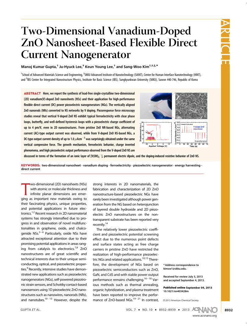
shown schematically in Figure 2a�e. Initially, a seedsolution of zinc acetate (0.04 M) was spin-coated on abare flexible ITO-coated plastic substrate. Subse-quently, zinc nitrate hexahydrate and hexamethylene-tetramine (HMT) was used for the growth of V-dopedZnO NS. The main growth of V-doped ZnO NS wasundertaken at 95 �C for 3 h (see Experiments andMethods). After the V doping, NR was completelyconverted into the 2D NS network by the followingtransition mechanisms. It is suggested that the forma-tion of ZnO NR or NS is closely associated with OH�
ligands.30,31 Generally, the growth habits of ZnO al-ways directly decide the final shape of the crystal,which in turn is greatly influenced by its growthconditions. In an aqueous solutionmethod, the growthof ZnO crystals is usually divided into two processes ofnucleation and growth. The formation of pristine ZnONRs can be described as the stacking of a number ofalternate planes with tetrahedrally coordinated O2�
and Zn2þ ions along the c-axis. ZnO has positivelycharged (0001) and negatively charged (0001) polarsurfaces, while the (0001)-Zn terminated surface ischemically active and the (0001)-O terminated surfaceis inert. Preferential growth of ZnO along the c-axis isenergetically favorable, which results in the formation1D nanostructures.32,33 During the growth of ZnO in thepresence of HMT, negative ions (OH� ions) are prefer-entially adsorbed to the (0001) plane and promote
Figure 2. (a�e) Schematic diagrams for thegrowthmechanismof V-dopedZnO. The seed layerwas depositedby spin coatingon a bare ITO/PET substrate. V(OH)4
� ions are connected at the Znþ terminated surface, which blocks the 1D growth ofV-doped ZnO. The resulting 2D formation was taken as a NS network. (f) Original image of vertically grown transparent andflexible V-doped ZnO NS on ITO/PET.
ARTIC
LE
GUPTA ET AL. VOL. 7 ’ NO. 10 ’ 8932–8939 ’ 2013
www.acsnano.org
8935
crystal growth along the c-axis direction. This anisotropygrowth is supported by the above-mentioned crystal-lographic habit of ZnO, so that 1D growth of the NRs inthe [0001] direction is preferred.On the other hand, in the growth procedure of the
NS, Zn ions exist in the form of Zn(OH)2 complex speciesserving as growth units for ZnO crystal growth in anydirection. The excessOH� ions are easily adsorbedon thepositively charged (0001) surface and the growth alongthe [0001] direction is partially restricted. The extrahydroxide ions in the V-doped ZnO NS in this presentcase are supposed to originate from a doping source(V2O5, vanadium pentoxide). Because the V elementundergoes chemical reactions under alkaline conditionsin the presence of amine (HMT) and is supposed to formthe vanadium hydroxide [V(OH)4
�], which can presum-ably bind to the positively charged Zn2þ-terminated(0001) polar surface of ZnO more strongly than to othernonpolar surfaces, the ZnO growth along the [0001]direction is effectively blocked, as shown schematicallyin Figure 2c�e. As a result, although the preferentialdirection of the c-axis is maintained as the crystal growthproceeds, thegrowth rate ratio of c-axis direction to othercrystallographic directions decreases greatly due to theshielding effect of [V(OH)4
�] ions on the (0001) surface,which allows the lateral growth to occur in the formof 2DNS.32�34 The original photo image of a flexible transpar-ent 2D V-doped ZnO NS sample is shown in Figure 2f.WeusedPFMto investigate thepiezoelectricbehaviorof
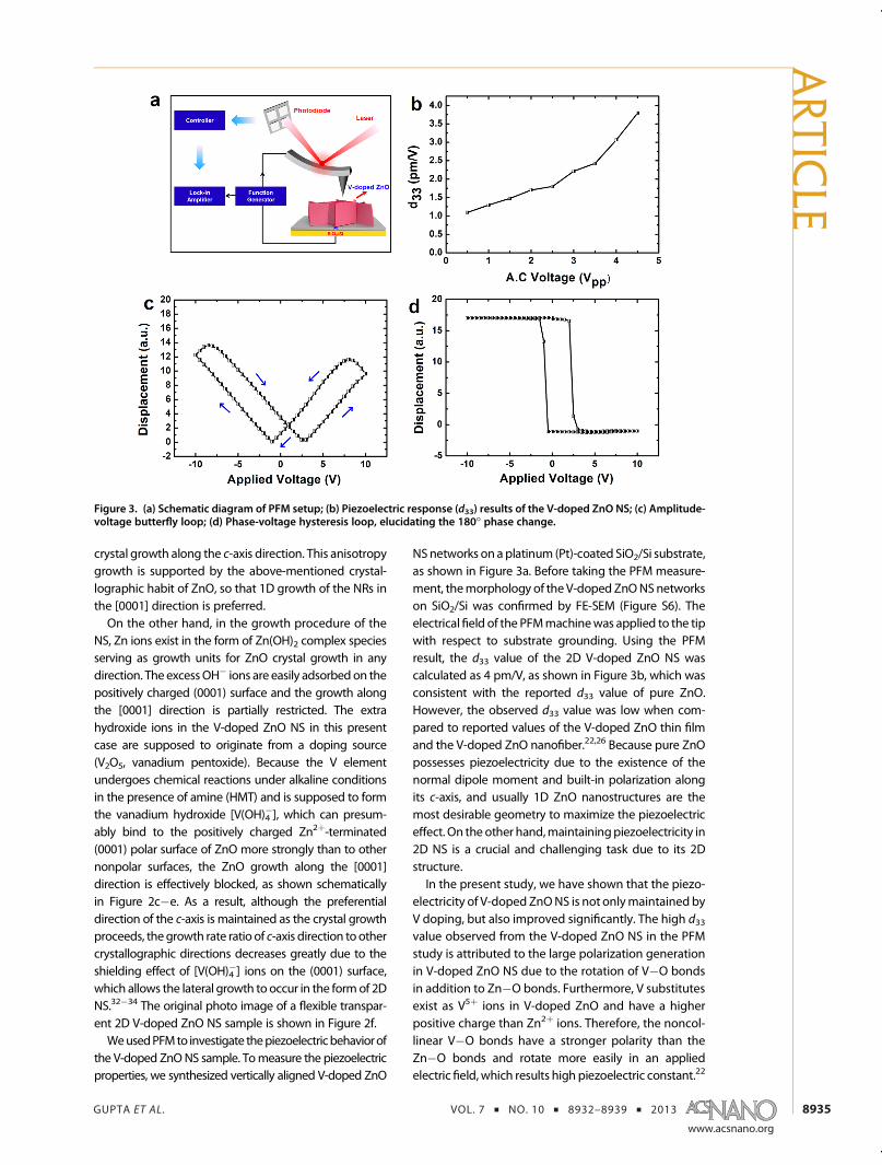
the V-doped ZnONS sample. Tomeasure the piezoelectricproperties, we synthesized vertically aligned V-doped ZnO
NSnetworks on a platinum (Pt)-coated SiO2/Si substrate,as shown in Figure 3a. Before taking the PFM measure-ment, themorphology of the V-doped ZnONSnetworkson SiO2/Si was confirmed by FE-SEM (Figure S6). Theelectricalfield of the PFMmachinewas applied to the tipwith respect to substrate grounding. Using the PFMresult, the d33 value of the 2D V-doped ZnO NS wascalculated as 4 pm/V, as shown in Figure 3b, which wasconsistent with the reported d33 value of pure ZnO.However, the observed d33 value was low when com-pared to reported values of the V-doped ZnO thin filmand the V-doped ZnO nanofiber.22,26 Because pure ZnOpossesses piezoelectricity due to the existence of thenormal dipole moment and built-in polarization alongits c-axis, and usually 1D ZnO nanostructures are themost desirable geometry to maximize the piezoelectriceffect. On the other hand,maintainingpiezoelectricity in2D NS is a crucial and challenging task due to its 2Dstructure.In the present study, we have shown that the piezo-
electricity of V-doped ZnONS is not onlymaintained byV doping, but also improved significantly. The high d33value observed from the V-doped ZnO NS in the PFMstudy is attributed to the large polarization generationin V-doped ZnO NS due to the rotation of V�O bondsin addition to Zn�O bonds. Furthermore, V substitutesexist as V5þ ions in V-doped ZnO and have a higherpositive charge than Zn2þ ions. Therefore, the noncol-linear V�O bonds have a stronger polarity than theZn�O bonds and rotate more easily in an appliedelectric field,which results high piezoelectric constant.22
Figure 3. (a) Schematic diagram of PFM setup; (b) Piezoelectric response (d33) results of the V-doped ZnO NS; (c) Amplitude-voltage butterfly loop; (d) Phase-voltage hysteresis loop, elucidating the 180� phase change.
ARTIC
LE
GUPTA ET AL. VOL. 7 ’ NO. 10 ’ 8932–8939 ’ 2013
www.acsnano.org
8936
In a further investigation based on the PFM measure-ments, V-doped ZnO NS showed butterfly loops andphase loops of the piezoelectric displacement as afunction of the applied dc bias voltage from �10 to 10 V,as shown in Figure 3c and d, respectively. The 2D V-dopedZnO NS clearly shows a distinct hysteresis and 180� phaseswitching, which can be illustrated by their ferroelectricbehavior.35
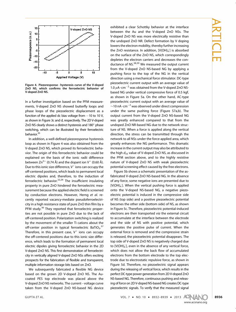
In addition, a well-defined piezoresponse hysteresisloop as shown in Figure 4 was also obtained from theV-doped ZnO NS, which proved its ferroelectric beha-vior. The origin of this ferroelectric behavior could beexplained on the basis of the ionic radii differencebetween Zn2þ (0.74 Å) and the dopant ion Vþ (0.60 Å).Due to this ionic size difference, Vþ ions can occupy theoff-centered positions, which leads to permanent localelectric dipoles and, therefore, to the induction offerroelectric behavior.22,26 The insufficient insulatingproperty in pure ZnO hindered the ferroelectric mea-surement because the applied electric field is screenedby conduction electrons. However, Herng et al. re-cently reported vacancy-mediate pseudoferroelectri-city in a high resistance state of pure ZnO thin film by aPFM study.36 They reported that ferroelectric proper-ties are not possible in pure ZnO due to the lack ofoff-centered position. Polarization switching is realizedby the movement of the smaller Ti cations about theoff-center position in typical ferroelectric BaTiO3.
37
Therefore, in this present case, Vþ ions can occupythe off-centered positions due to this ionic size differ-ence, which leads to the formation of permanent localelectric dipoles giving ferroelectric behavior in the 2DV-doped ZnO NS. This first demonstration of ferroelectri-city in vertically aligned V-doped ZnO NSs offers excitingprospects for the fabrication of flexible and transparent,multiple information storage bits based on ZnO.We subsequently fabricated a flexible NG device
based on the grown 2D V-doped ZnO NS. The Au-coated PES top electrode was placed above theV-doped ZnO NS networks. The current�voltage curvetaken from the V-doped ZnO NS-based NG device
exhibited a clear Schottky behavior at the interfacebetween the Au and the V-doped ZnO NSs. TheV-doped ZnO NS was more electrically resistive thanthe undoped ZnO NR. Defect formation by V dopinglowers the electronmobility, thereby further increasingthe ZnO resistance. In addition, [V(OH)4
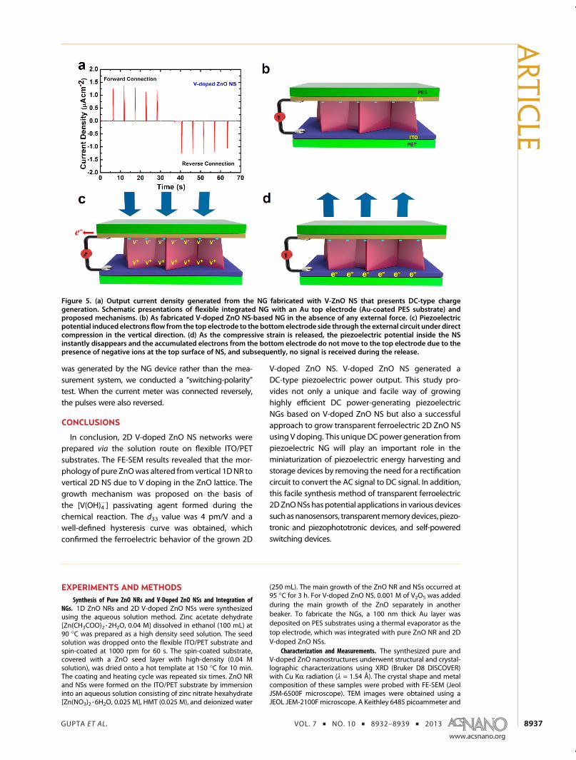
�] is absorbedon the surface of the ZnO NS, which correspondinglydepletes the electron carriers and decreases the con-ductance of NS.38,39 We measured the output currentfrom the V-doped ZnO NS-based NG by applying apushing force to the top of the NG in the verticaldirection using a mechanical force stimulator. DC-typepiezoelectric current output with an average value of1.0 μA 3 cm
�2 was obtained from the V-doped ZnO NS-based NG under vertical compressive force of 0.5 kgf,as shown in Figure 5a. On the other hand, AC-typepiezoelectric current output with an average value of∼10 nA 3 cm
�2 was observed under direct compressionunder the same pushing force (Figure S7a,b). Theoutput current from the V-doped ZnO NS-based NGwas greatly enhanced compared to that from theundoped ZnO NR-based NG due to the network struc-ture of NS. When a force is applied along the verticaldirection, the stress can be transmitted through thenetwork to all NSs under the force-applied area, whichgreatly enhances the NG performance. This dramaticincrease in the current outputmay also be attributed tothe high d33 value of V-doped ZnO NS, as discussed inthe PFM section above, and to the highly resistivenature of V-doped ZnO NS with weak piezoelectricpotential screening effect caused by the free electrons.Figure 5b shows a schematic presentation of the as-
fabricated V-doped ZnO NS-based NG. In the absenceof any force, some negative ions are presented due to[V(OH)4
�]. When the vertical pushing force is appliedonto the V-doped NS-based NG, a negative piezo-electric potential is induced in the compressive sideof NS (top side) and a positive piezoelectric potentialbecomes the other side (bottom side) of NS, as shownin Figure 5c. Therefore, piezoelectric potential-inducedelectrons are then transported via the external circuitto accumulate at the interface between the electrodeand the side of NS with positive potential, whichgenerates the positive pulse of current. When theexternal force is removed and the compressive strainis released, the piezoelectric potential disappears. Thetop side of V-doped ZnO NS is negatively charged dueto [V(OH)4
�], even in the absence of any vertical force,which does not allow the back flow of accumulatedelectrons from the bottom electrode to the top elec-trode due to electrostatic repulsive force, as shown inFigure 5d. Therefore, no piezoelectric signal appearsduring the releasing of vertical force, which results in theperfect DC-typepower generation from2DV-dopedZnONS-based NG. Therefore, continuous pushing and releas-ing of force on 2DV-dopedNS-basedNGcreatesDC-typepiezoelectric signals. To verify that the measured signal
Figure 4. Piezoresponse�hysteresis curve of the V-dopedZnO NS, which confirms the ferroelectric behavior ofV-doped ZnO NS.
ARTIC
LE
GUPTA ET AL. VOL. 7 ’ NO. 10 ’ 8932–8939 ’ 2013
www.acsnano.org
8937
was generated by the NG device rather than the mea-surement system, we conducted a “switching-polarity”test. When the current meter was connected reversely,the pulses were also reversed.
CONCLUSIONS
In conclusion, 2D V-doped ZnO NS networks wereprepared via the solution route on flexible ITO/PETsubstrates. The FE-SEM results revealed that the mor-phology of pure ZnOwas altered from vertical 1DNR tovertical 2D NS due to V doping in the ZnO lattice. Thegrowth mechanism was proposed on the basis ofthe [V(OH)4
�] passivating agent formed during thechemical reaction. The d33 value was 4 pm/V and awell-defined hysteresis curve was obtained, whichconfirmed the ferroelectric behavior of the grown 2D
V-doped ZnO NS. V-doped ZnO NS generated aDC-type piezoelectric power output. This study pro-vides not only a unique and facile way of growinghighly efficient DC power-generating piezoelectricNGs based on V-doped ZnO NS but also a successfulapproach to grow transparent ferroelectric 2D ZnO NSusing V doping. This unique DC power generation frompiezoelectric NG will play an important role in theminiaturization of piezoelectric energy harvesting andstorage devices by removing the need for a rectificationcircuit to convert the AC signal to DC signal. In addition,this facile synthesis method of transparent ferroelectric2DZnONSs has potential applications in various devicessuchasnanosensors, transparentmemorydevices, piezo-tronic and piezophototronic devices, and self-poweredswitching devices.
EXPERIMENTS AND METHODSSynthesis of Pure ZnO NRs and V-Doped ZnO NSs and Integration of
NGs. 1D ZnO NRs and 2D V-doped ZnO NSs were synthesizedusing the aqueous solution method. Zinc acetate dehydrate[Zn(CH3COO)2 3 2H2O, 0.04 M] dissolved in ethanol (100 mL) at90 �C was prepared as a high density seed solution. The seedsolution was dropped onto the flexible ITO/PET substrate andspin-coated at 1000 rpm for 60 s. The spin-coated substrate,covered with a ZnO seed layer with high-density (0.04 Msolution), was dried onto a hot template at 150 �C for 10 min.The coating and heating cycle was repeated six times. ZnO NRand NSs were formed on the ITO/PET substrate by immersioninto an aqueous solution consisting of zinc nitrate hexahydrate[Zn(NO3)2 3 6H2O, 0.025 M], HMT (0.025 M), and deionized water
(250 mL). The main growth of the ZnO NR and NSs occurred at95 �C for 3 h. For V-doped ZnO NS, 0.001 M of V2O5 was addedduring the main growth of the ZnO separately in anotherbeaker. To fabricate the NGs, a 100 nm thick Au layer wasdeposited on PES substrates using a thermal evaporator as thetop electrode, which was integrated with pure ZnO NR and 2DV-doped ZnO NSs.
Characterization and Measurements. The synthesized pure andV-doped ZnO nanostructures underwent structural and crystal-lographic characterizations using XRD (Bruker D8 DISCOVER)with Cu KR radiation (λ = 1.54 Å). The crystal shape and metalcomposition of these samples were probed with FE-SEM (JeolJSM-6500F microscope). TEM images were obtained using aJEOL JEM-2100F microscope. A Keithley 6485 picoammeter and
Figure 5. (a) Output current density generated from the NG fabricated with V-ZnO NS that presents DC-type chargegeneration. Schematic presentations of flexible integrated NG with an Au top electrode (Au-coated PES substrate) andproposed mechanisms. (b) As fabricated V-doped ZnO NS-based NG in the absence of any external force. (c) Piezoelectricpotential induced electronsflow from the top electrode to the bottomelectrode side through the external circuit under directcompression in the vertical direction. (d) As the compressive strain is released, the piezoelectric potential inside the NSinstantly disappears and the accumulated electrons from the bottom electrode do not move to the top electrode due to thepresence of negative ions at the top surface of NS, and subsequently, no signal is received during the release.
ARTIC
LE
GUPTA ET AL. VOL. 7 ’ NO. 10 ’ 8932–8939 ’ 2013
www.acsnano.org
8938
2182A voltmeter were used to measure the low-noise outputcurrent and voltage generated from the piezoelectric NGs,respectively.
Conflict of Interest: The authors declare no competingfinancial interest.
Acknowledgment. This work was financially supported byBasic Science Research Program through the National ResearchFoundation (NRF) ofKoreaGrant fundedby theMinistryofScience,ICT and Future Planning (2012R1A2A1A01002787, 2010-0019086,2009-0083540), and the Energy International Collaboration Re-search and Development Program of the Korea Institute of EnergyTechnology Evaluation and Planning (KETEP) funded by theMinistry of Knowledge Economy (MKE; 2011-8520010050).
Supporting Information Available: Low-resolution FE-SEMimage of V-doped ZnO NS and cross-sectional FE-SEM imageof V-doped ZnO NS networks. Cross-sectional FE-SEM image ofpure ZnO NRs. EDS spectrum of the V-doped ZnO NSs. Widescan XPS pattern of V-doped ZnO NS on ITO/PET substrate.FE-SEM image of 2D V-doped ZnO NS networks on a Pt/SiO2/Sisubstrate. Schematic diagram of flexible ZnO NR-based NG andpiezoelectric output current output from under a verticalcompressive force of 0.5 kgf. This material is available free ofcharge via the Internet at http://pubs.acs.org.
REFERENCES AND NOTES1. Service, R. F. Carbon Sheets an Atom Thick Give Rise to
Graphene Dreams. Science 2009, 324, 875–877.2. Lee, K. H.; Shin, H. J.; Lee, J.; Lee, I.; Kim, G. H.; Choi, J. Y.; Kim,
S.-W. Large-Scale Synthesis of High-Quality HexagonalBoron Nitride Nanosheets for Large-Area Graphene Elec-tronics. Nano Lett. 2012, 12, 714–718.
3. Huang, X.; Zeng, Z.; Fan, Z.; Liu, J.; Zhang, H. Graphene-Based Electrodes. Adv. Mater. 2012, 24, 5979–6004.
4. Bitounis, D.; Boucetta, H. A.; Hong, B. H.; Min, D. H.;Kostarelos, K. Prospects and Challenges of Graphene inBiomedical Applications. Adv. Mater. 2013, 25, 2258–2268.
5. Lee, H. S.; Min, S. W.; Chang, Y. G.; Park, M. K.; Nam, T.; Kim,H.; Kim, J. H.; Ryu, S.; Im, S. MoS2 Nanosheet Phototransis-tors with Thickness-Modulated Optical Energy Gap. NanoLett. 2012, 12, 3695–3700.
6. Li, C.; Huang, L.; Snigdha, G. P.; Yu, Y.; Cao, L. Role ofBoundary Layer Diffusion in Vapor Deposition Growth ofChalcogenide Nanosheets: The Case of GeS. ACS Nano2012, 6, 8868–8877.
7. Tagusagawa, C.; Takagaki, A.; Hayashi, S.; Domen, K. Char-acterization of HNbWO6 and HTaWO6 Metal Oxide Nano-sheet Aggregates As Solid Acid Catalysts. J. Phys. Chem. C2009, 113, 7831–7837.
8. Osada, M.; Sasaki, T. Exfoliated Oxide Nanosheets: NewSolution to Nanoelectronics. J. Mater. Chem. 2009, 19,2503–2511.
9. Wang, Z. L.; Kong, X. Y.; Ding, Y.; Gao, P.; Hughes, W. L.;Yang, R.; Zhang, Y. Semiconducting and PiezoelectricOxide Nanostructures Induced by Polar Surfaces. Adv.Funct. Mater. 2004, 14, 943–956.
10. Park, H. K.; Lee, K. Y.; Seo, J.-S.; Jeong, J. A.; Kim, H. K.; Choi,D.; Kim, S.-W. Charge- Generating Mode Control in High-Performance Transparent Flexible Piezoelectric Nano-generators. Adv. Funct. Mater. 2011, 21, 1187–1193.
11. Zhou, J.; Gu, Y.; Fei, P.; Mai, W.; Gao, Y.; Yang, R.; Bao, G.;Wang, Z. L. Flexible Piezotronic Strain Sensor. Nano Lett.2008, 8, 3035–3040.
12. Pan, C.; Yu, R.; Niu, S.; Zhu, G.; Wang, Z. L. Piezotronic Effecton the Sensitivity and Signal Level of Schottky ContactedProactive Micro/Nanowire Nanosensors. ACS Nano 2013,7, 1803–1810.
13. Xi, Y.; Song, J.; Xu, S.; Yang, R.; Gao, Z.; Hu, C.;Wang, Z. L.Growthof ZnO Nanotube Arrays and Nanotube Based PiezoelectricNanogenerators. J. Mater. Chem. 2009, 19, 9260–9264.
14. Kim, K. H.; Kumar, B.; Lee, K. Y.; Park, H. K.; Lee, J. H.; Lee, H. H.;Jun, H.; Lee, D.; Kim, S.-W. Piezoelectric Two-DimensionalNanosheets/Anionic Layer Heterojunction for Efficient Di-rect Current Power Generation. Sci. Rep. 2013, 3, 2017.
15. Gao, Y.; Wang, Z. L. Equilibrium Potential of Free ChargeCarriers in a Bent Piezoelectric Semiconductive Nanowire.Nano Lett. 2009, 9, 1103–1110.
16. Kumar, B.; Lee, K. Y.; Park, H.-K.; Chae, S. J.; Lee, Y. H.; Kim, S.-W.Controlled Growth of Semiconducting Nanowire, Nano-wall, and Hybrid Nanostructures on Graphene for Piezo-electric Nanogenerators. ACS Nano 2011, 5, 4197–4204.
17. Huang, C. T.; Song, J.; Lee, W. F.; Ding, Y.; Gao, Z.; Hao, Y.;Chen, L. J.;Wang, Z. L. GaNNanowireArrays for High-OutputNanogenerators. J. Am. Chem. Soc. 2010, 132, 4766–4771.
18. Lin, Y. F.; Song, J.; Ding, Y.; Lu, S. Y.; Wang, Z. L. PiezoelectricNanogenerator Using Cds Nanowires. Appl. Phys. Lett.2008, 92, 022105.
19. Hu, Y.; Lin, L.; Zhang, Y.; Wang, Z. L. Replacing a Battery by aNanogenerator with 20 V Output. Adv. Mater. 2012, 24,110–114.
20. Pham, T. T.; Lee, K. Y.; Lee, J.-H.; Kim, K. H.; Shin, K. S.; Gupta,M. K.; Kumar, B.; Kim, S.-W. Reliable Operation of a Nano-generator under Ultraviolet Light via Engineering Piezo-electric Potential. Energy Environ. Sci. 2013, 6, 841–846.
21. Lee, K. Y.; Kumar, B.; Seo, J.-S.; Kim, K.-H.; Sohn, J. I.; Cha,S. N.; Choi, D.; Wang, Z. L.; Kim, S.-W. p-Type Polymer-Hybridized High-Performance Piezoelectric Nanogenera-tors. Nano Lett. 2012, 12, 1959–1964.
22. Chen, Y. Q.; Zheng, X. J.; Feng, X. The Fabrication ofVanadium-Doped ZnO Piezoelectric Nanofiber by Electro-spinning. Nanotechnology 2010, 21, 055708–4.
23. Radovanovic, P. V.; Gamelin, D. R. High-Temperature Fer-romagnetism in Ni2þ-Doped ZnO Aggregates Preparedfrom Colloidal DilutedMagnetic Semiconductor QuantumDots. Phys. Rev. Lett. 2003, 19, 157202.
24. Tsukazaki, A.; Ohtomo, A.; Onuma, T.; Ohtani, M.; Makino,T.; Sumiya, M.; Ohtani, K.; Chichibu, S. F.; Fuke, S.; Segawa,Y.; et al. Repeated Temperature Modulation Epitaxy forp-Type Doping and Light-Emitting Diode Based on ZnO.Nat. Mater. 2005, 4, 42–46.
25. Yang, Y.; Pradel, K. C.; Jing, Q.; Wu, J. M.; Zhang, F.; Zhou, Y.;Zhang, Y.; Wang, Z. L. Thermoelectric NanogeneratorsBased on Single Sb-Doped ZnO Micro/Nanobelts. ACSNano 2012, 6, 6984–6989.
26. Yang, Y. C.; Song, C.; Wang, X. H.; Zeng, F.; Pan, F. GiantPiezoelectric d33 Coefficient in Ferroelectric VanadiumDoped ZnO Films. Appl. Phys. Lett. 2008, 92, 012907.
27. Wang, X.; Song, J.; Liu, J.; Wang, Z. L. Direct-Current Nano-generator Driven by Ultrasonic Waves. Science 2007, 316,102–105.
28. Liu, H.; Wu, Y.; Zhang, J. A New Approach toward Carbon-Modified Vanadium-Doped Titanium Dioxide Photocata-lysts. ACS Appl. Mater. Interfaces 2011, 3, 1757–1764.
29. Bondarenka, V.; Grebinskij, S.; Kaciulis, S.; Mattogno, G.;Mickevicius, S.; Vardauskas, H.; Volkov, V.; Zakharova, G.XPS Study of Vanadium-Yttrium Hydrates. J. ElectronSpectrosc. Relat. Phenom. 2001, 120, 131–135.
30. Cao, B.; Cai, W. From ZnO Nanorods to Nanoplates:Chemical Bath Deposition Growth and Surface-RelatedEmissions. J. Phys. Chem. C 2008, 112, 680–685.
31. Sun, Y.; Riley, D. J.; Ashfold, M. N. R. Mechanism of ZnONanotube Growth by Hydrothermal Methods on ZnO Film-CoatedSi Substrates. J. Phys. Chem.B2006,110, 15186–15192.
32. Vohs, J. M.; Barteau, M. A. Conversion of Methanol, For-maldehyde and Formic Acid on the Polar Faces of ZincOxide. Surf. Sci. 1986, 176, 91–114.
33. Dulub, O.; Diebold, U.; Kresse, G. Novel Stabilization Me-chanism on Polar Surfaces: ZnO(0001)-Zn. Phys. Rev. Lett.2003, 90, 016102.
34. Ye, C.; Bando, Y.; Shen, G.; Golberg, D. Thickness-DependentPhotocatalytic Performance of ZnO Nanoplatelets.J. Phys. Chem. B 2006, 110, 15146–15151.
35. Wang, Z.; Hu, J.; Yu, M. F. One-Dimensional FerroelectricMonodomain Formation in Single Crystalline BaTiO3
Nanowire. Appl. Phys. Lett. 2006, 89, 263119.36. Herng, T. S.; Kumar, A.; Ong, C. S.; Feng, Y. P.; Lu, Y. H.; Zeng,
K. Y.; Ding, J. Investigation of the Non-Volatile ResistanceChange in Noncentrosymmetric Compounds. Sci. Rep.2012, 2, 587.
ARTIC
LE

GUPTA ET AL. VOL. 7 ’ NO. 10 ’ 8932–8939 ’ 2013
www.acsnano.org
8939
37. Callister, W. D.; Rethwisch, D. G. Materials Science andEngineering; Wiley: New York, 2010.
38. Li, Q. H.; Gao, T.; Wang, Y. G.; Wang, T. H. Adsorption andDesorption of Oxygen Probed from ZnO Nanowire Filmsby Photocurrent Measurements. Appl. Phys. Lett. 2005, 86,123117.
39. Weissenberger, D.; Dürrschnabel, M.; Gerthsen, D.; Willard,F. P.; Reiser, A.; Prinz, G. M.; Feneberg, M.; Thonke, K.; Sauer,R. Conductivity of Single ZnO Nanorods after Ga Implanta-tion in a Focused-Ion-Beam System. Appl. Phys. Lett. 2007,91, 132110.
ARTIC
LE