Embed Size (px)
Citation preview
Two Phase, Three Legs Inverter with Z-Source
Input Impedance
Ghassan A. Hameed, Mahmood N. Abed, and Ibrahim Mahariq Electrical and Electronic Engineering Faculty, University of Turkish Aeronautical Association, Turkey
Email: ghassanali72, [email protected], [email protected]
Index Terms—z-source, shoot- through,
switches
I. INTRODUCTION
The two phase inverter is used to drive the two phase
induction motors that was supplied in past from four wires
networks of two phases source. In the industrial and
residential applications, that is very cost to use three phase
induction machines because of high cost of their power
electronic circuits. Today, two phase drives are developed
and produced in low cost [1]. One of these new drives is
two phase inverter with (90o) between each phase with
three legs and two legs circuit and Z-source property
investment to raise the voltage output of the inverter.
Selection of switches for example (transistors, mosfet's,
IGBT) that will derive the inverter circuit is very
important, and selection of modulation type ,for example
(SPWM) or space vector pulse width modulation
(SVPWM) is very important for the building the inverter
circuit that will be used for driving, because it will specify
the output shape of inverter and its value.
II. TWO PHASE, TWO LEGS INVERTER
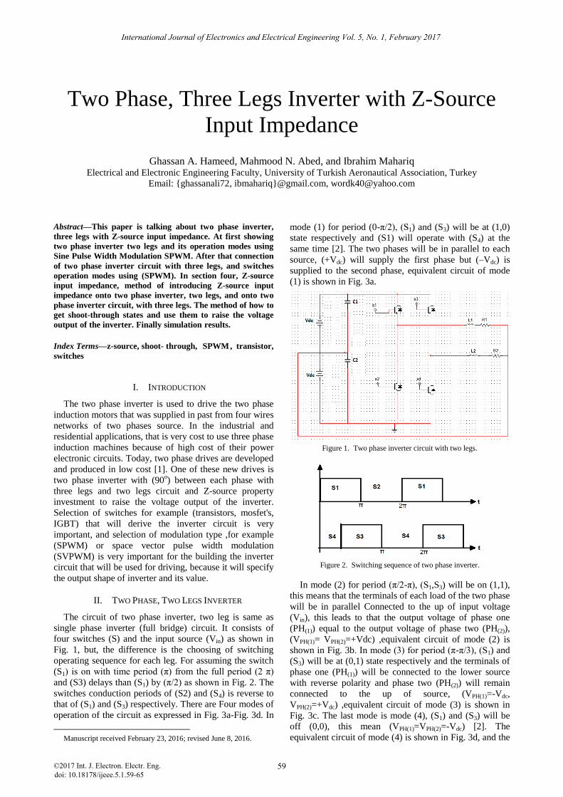
The circuit of two phase inverter, two leg is same as
single phase inverter (full bridge) circuit. It consists of
four switches (S) and the input source (Vin) as shown in
Fig. 1, but, the difference is the choosing of switching
operating sequence for each leg. For assuming the switch
(S1) is on with time period (π) from the full period (2 π)
and (S3) delays than (S1) by (π/2) as shown in Fig. 2. The
switches conduction periods of (S2) and (S4) is reverse to
that of (S1) and (S3) respectively. There are Four modes of
operation of the circuit as expressed in Fig. 3a-Fig. 3d. In
Manuscript received February 23, 2016; revised June 8, 2016.
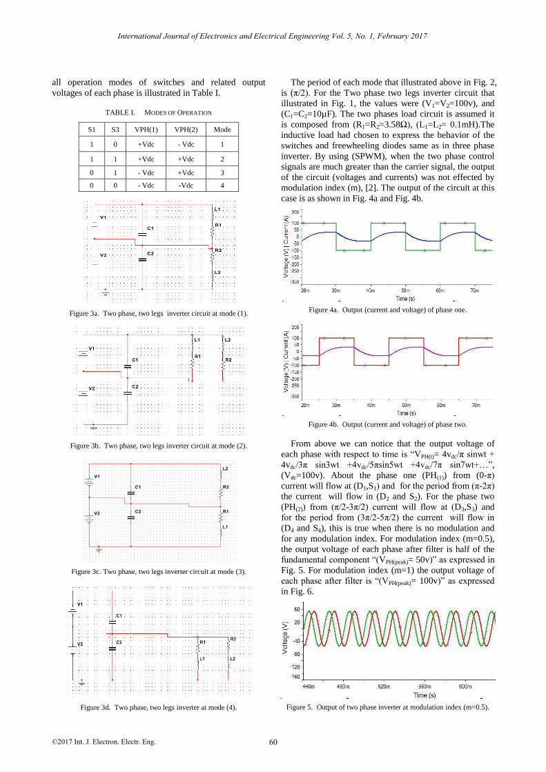
mode (1) for period (0-π/2), (S1) and (S3) will be at (1,0)
state respectively and (S1) will operate with (S4) at the
same time [2]. The two phases will be in parallel to each
source, (+Vdc) will supply the first phase but (–Vdc) is
supplied to the second phase, equivalent circuit of mode
(1) is shown in Fig. 3a.
Figure 1. Two phase inverter circuit with two legs.
Figure 2. Switching sequence of two phase inverter.
In mode (2) for period (π/2-π), (S1,S3) will be on (1,1),
this means that the terminals of each load of the two phase
will be in parallel Connected to the up of input voltage
(Vin), this leads to that the output voltage of phase one
(PH(1)) equal to the output voltage of phase two (PH(2)),
(VPH(1)= VPH(2)=+Vdc) ,equivalent circuit of mode (2) is
shown in Fig. 3b. In mode (3) for period (π-π/3), (S1) and
(S3) will be at (0,1) state respectively and the terminals of
phase one (PH(1)) will be connected to the lower source
with reverse polarity and phase two (PH(2)) will remain
connected to the up of source, (VPH(1)=-Vdc,
VPH(2)=+Vdc) ,equivalent circuit of mode (3) is shown in
Fig. 3c. The last mode is mode (4), (S1) and (S3) will be
off (0,0), this mean (VPH(1)=VPH(2)=-Vdc) [2]. The
equivalent circuit of mode (4) is shown in Fig. 3d, and the
International Journal of Electronics and Electrical Engineering Vol. 5, No. 1, February 2017
©2017 Int. J. Electron. Electr. Eng. 59doi: 10.18178/ijeee.5.1.59-65
SPWM , transistor,
Abstract—This paper is talking about two phase inverter,
three legs with Z-source input impedance. At first showing
two phase inverter two legs and its operation modes using
Sine Pulse Width Modulation SPWM. After that connection
of two phase inverter circuit with three legs, and switches
operation modes using (SPWM). In section four, Z-source
input impedance, method of introducing Z-source input
impedance onto two phase inverter, two legs, and onto two
phase inverter circuit, with three legs. The method of how to
get shoot-through states and use them to raise the voltage
output of the inverter. Finally simulation results.
all operation modes of switches and related output
voltages of each phase is illustrated in Table I.
TABLE I. MODES OF OPERATION
S1 S3 VPH(1) VPH(2) Mode
1 0 +Vdc - Vdc 1
1 1 +Vdc +Vdc 2
0 1 - Vdc +Vdc 3
0 0 - Vdc -Vdc 4
Figure 3a. Two phase, two legs inverter circuit at mode (1).
Figure 3b. Two phase, two legs inverter circuit at mode (2).
Figure 3c. Two phase, two legs inverter circuit at mode (3).
Figure 3d. Two phase, two legs inverter at mode (4).
The period of each mode that illustrated above in Fig. 2,
is (π/2). For the Two phase two legs inverter circuit that
illustrated in Fig. 1, the values were (V1=V2=100v), and
(C1=C2=10µF). The two phases load circuit is assumed it
is composed from (R1=R2=3.58Ω), (L1=L2= 0.1mH).The
inductive load had chosen to express the behavior of the
switches and freewheeling diodes same as in three phase
inverter. By using (SPWM), when the two phase control
signals are much greater than the carrier signal, the output
of the circuit (voltages and currents) was not effected by
modulation index (m), [2]. The output of the circuit at this
case is as shown in Fig. 4a and Fig. 4b.
Figure 4a. Output (current and voltage) of phase one.
Figure 4b. Output (current and voltage) of phase two.
From above we can notice that the output voltage of
each phase with respect to time is “VPH(t)= 4vdc/π sinwt +
4vdc/3π sin3wt +4vdc/5πsin5wt +4vdc/7π sin7wt+…”,
(Vdc=100v). About the phase one (PH(1)) from (0-π)
current will flow at (D1,S1) and for the period from (π-2π)
the current will flow in (D2 and S2). For the phase two
(PH(2)) from (π/2-3π/2) current will flow at (D3,S3) and
for the period from (3π/2-5π/2) the current will flow in
(D4 and S4), this is true when there is no modulation and
for any modulation index. For modulation index (m=0.5),
the output voltage of each phase after filter is half of the
fundamental component “(VPH(peak)= 50v)” as expressed in
Fig. 5. For modulation index (m=1) the output voltage of
each phase after filter is “(VPH(peak)= 100v)” as expressed
in Fig. 6.
Figure 5. Output of two phase inverter at modulation index (m=0.5).
International Journal of Electronics and Electrical Engineering Vol. 5, No. 1, February 2017
©2017 Int. J. Electron. Electr. Eng. 60
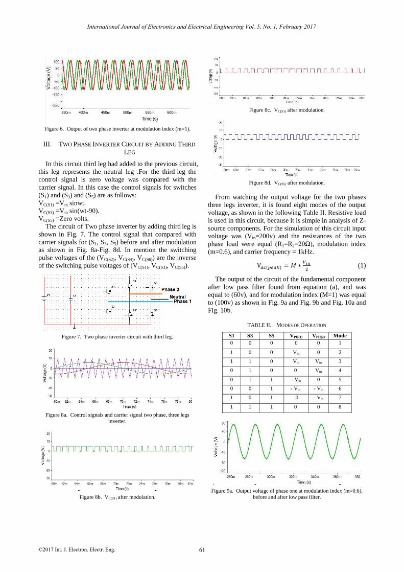
Figure 6. Output of two phase inverter at modulation index (m=1).
III. TWO PHASE INVERTER CIRCUIT BY ADDING THIRD
LEG
In this circuit third leg had added to the previous circuit,
this leg represents the neutral leg .For the third leg the
control signal is zero voltage was compared with the
carrier signal. In this case the control signals for switches
(S1) and (S3) and (S5) are as follows:
VC(S1) =Vm sinwt.
VC(S3) =Vm sin(wt-90).
VC(S5) =Zero volts.
The circuit of Two phase inverter by adding third leg is
shown in Fig. 7. The control signal that compared with
carrier signals for (S1, S3, S5) before and after modulation
as shown in Fig. 8a-Fig. 8d. In mention the switching
pulse voltages of the (VC(S2), VC(S4), VC(S6)) are the inverse
of the switching pulse voltages of (VC(S1), VC(S3), VC(S5)).
Figure 7. Two phase inverter circuit with third leg.
Figure 8a. Control signals and carrier signal two phase, three legs
inverter.
Figure 8b. VC(S1) after modulation.
Figure 8c. VC(S3) after modulation.
Figure 8d. VC(S5) after modulation.
From watching the output voltage for the two phases
three legs inverter, it is found eight modes of the output
voltage, as shown in the following Table II. Resistive load
is used in this circuit, because it is simple in analysis of Z-
source components. For the simulation of this circuit input
voltage was (Vin=200v) and the resistances of the two
phase load were equal (R1=R2=20Ω), modulation index
(m=0.6), and carrier frequency = 1kHz.
V𝑎𝑐(𝑝𝑒𝑎𝑘) = 𝑀 ∗𝑉𝑖𝑛
2 (1)
The output of the circuit of the fundamental component
after low pass filter found from equation (a), and was
equal to (60v), and for modulation index (M=1) was equal
to (100v) as shown in Fig. 9a and Fig. 9b and Fig. 10a and
Fig. 10b.
TABLE II. MODES OF OPERATION
Mode VPH(2) VPH(1) S5 S3 S1
1 0 0 0 0 0
2 0 Vin 0 0 1
3 Vin Vin 0 1 1
4 Vin 0 0 1 0
5 0 - Vin 1 1 0
6 - Vin - Vin 1 0 0
7 - Vin 0 1 0 1
8 0 0 1 1 1
Figure 9a. Output voltage of phase one at modulation index (m=0.6), before and after low pass filter.
International Journal of Electronics and Electrical Engineering Vol. 5, No. 1, February 2017
©2017 Int. J. Electron. Electr. Eng. 61
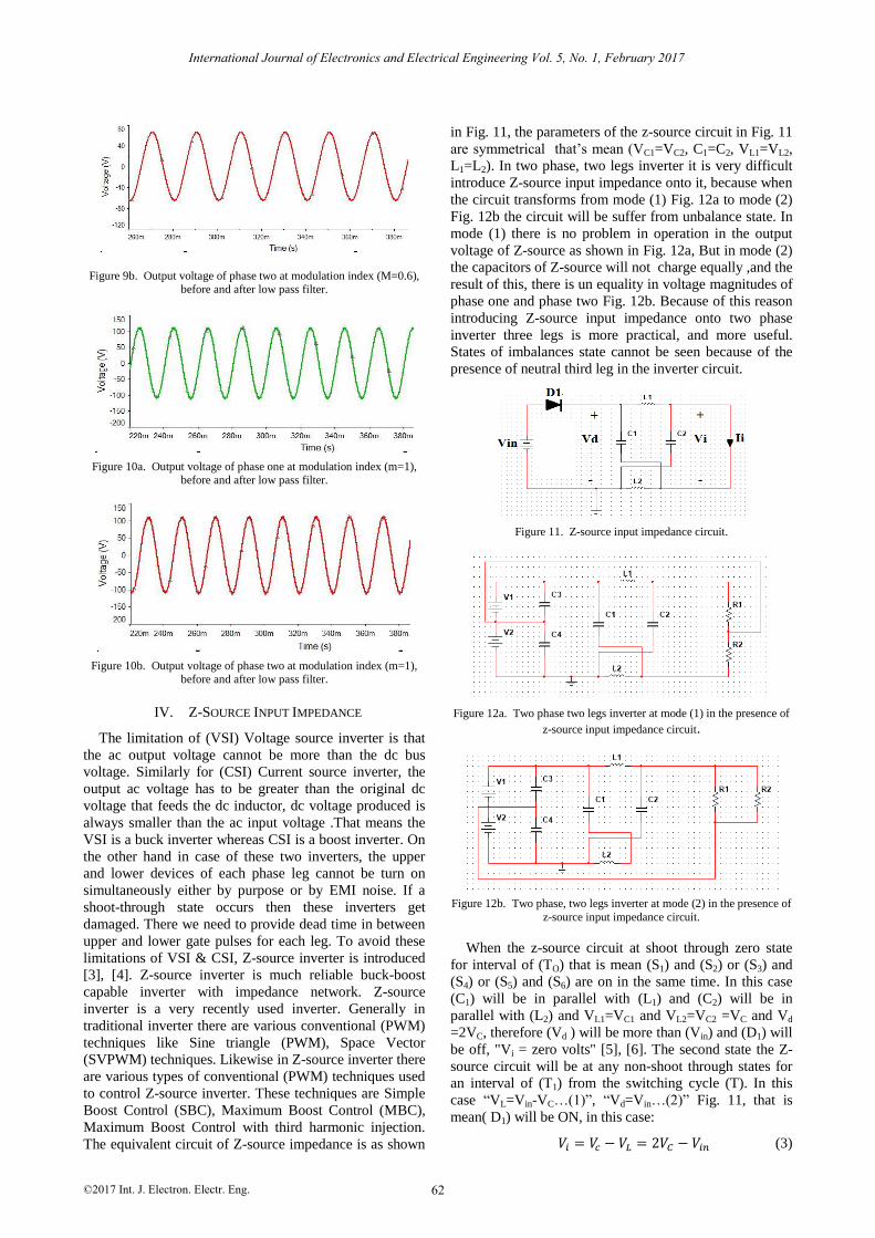
Figure 9b. Output voltage of phase two at modulation index (M=0.6), before and after low pass filter.
Figure 10a. Output voltage of phase one at modulation index (m=1), before and after low pass filter.
Figure 10b. Output voltage of phase two at modulation index (m=1), before and after low pass filter.
IV. Z-SOURCE INPUT IMPEDANCE
The limitation of (VSI) Voltage source inverter is that
the ac output voltage cannot be more than the dc bus
voltage. Similarly for (CSI) Current source inverter, the
output ac voltage has to be greater than the original dc
voltage that feeds the dc inductor, dc voltage produced is
always smaller than the ac input voltage .That means the
VSI is a buck inverter whereas CSI is a boost inverter. On
the other hand in case of these two inverters, the upper
and lower devices of each phase leg cannot be turn on
simultaneously either by purpose or by EMI noise. If a
shoot-through state occurs then these inverters get
damaged. There we need to provide dead time in between
upper and lower gate pulses for each leg. To avoid these
limitations of VSI & CSI, Z-source inverter is introduced
[3], [4]. Z-source inverter is much reliable buck-boost
capable inverter with impedance network. Z-source
inverter is a very recently used inverter. Generally in
traditional inverter there are various conventional (PWM)
techniques like Sine triangle (PWM), Space Vector
(SVPWM) techniques. Likewise in Z-source inverter there
are various types of conventional (PWM) techniques used
to control Z-source inverter. These techniques are Simple
Boost Control (SBC), Maximum Boost Control (MBC),
Maximum Boost Control with third harmonic injection.
The equivalent circuit of Z-source impedance is as shown
in Fig. 11, the parameters of the z-source circuit in Fig. 11
are symmetrical that’s mean (VC1=VC2, C1=C2, VL1=VL2,
L1=L2). In two phase, two legs inverter it is very difficult
introduce Z-source input impedance onto it, because when
the circuit transforms from mode (1) Fig. 12a to mode (2)
Fig. 12b the circuit will be suffer from unbalance state. In
mode (1) there is no problem in operation in the output
voltage of Z-source as shown in Fig. 12a, But in mode (2)
the capacitors of Z-source will not charge equally ,and the
result of this, there is un equality in voltage magnitudes of
phase one and phase two Fig. 12b. Because of this reason
introducing Z-source input impedance onto two phase
inverter three legs is more practical, and more useful.
States of imbalances state cannot be seen because of the
presence of neutral third leg in the inverter circuit.
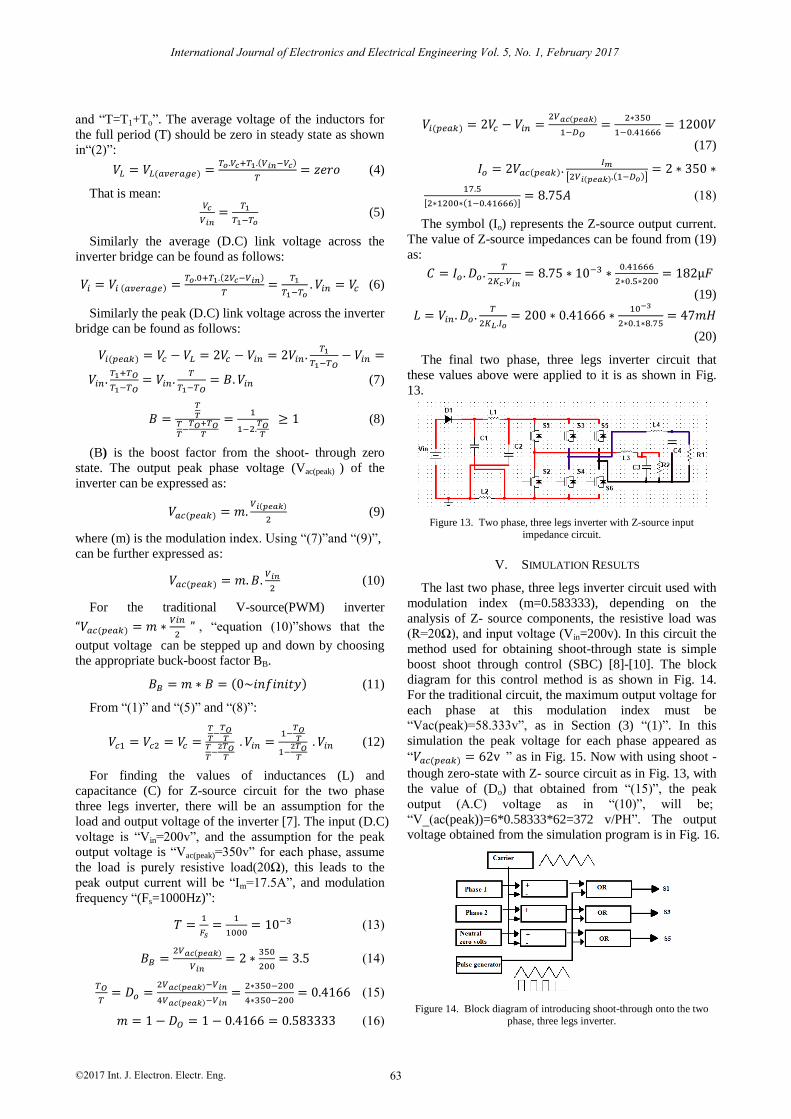
Figure 11. Z-source input impedance circuit.
Figure 12a. Two phase two legs inverter at mode (1) in the presence of
z-source input impedance circuit.
Figure 12b. Two phase, two legs inverter at mode (2) in the presence of
z-source input impedance circuit.
𝑉𝑖 = 𝑉𝑐 − 𝑉𝐿 = 2𝑉𝐶 − 𝑉𝑖𝑛 (3)
International Journal of Electronics and Electrical Engineering Vol. 5, No. 1, February 2017
©2017 Int. J. Electron. Electr. Eng. 62
When the z-source circuit at shoot through zero state
for interval of (TO) that is mean (S1) and (S2) or (S3) and
(S4) or (S5) and (S6) are on in the same time. In this case
(C1) will be in parallel with (L1) and (C2) will be in
parallel with (L2) and VL1=VC1 and VL2=VC2 =VC and Vd
=2VC, therefore (Vd ) will be more than (Vin) and (D1) will
be off, "Vi = zero volts" [5], [6]. The second state the Z-
source circuit will be at any non-shoot through states for
an interval of (T1) from the switching cycle (T). In this
case “VL=Vin-VC…(1)”, “Vd=Vin…(2)” Fig. 11, that is
mean( D1) will be ON, in this case:
International Journal of Electronics and Electrical Engineering Vol. 5, No. 1, February 2017
©2017 Int. J. Electron. Electr. Eng. 63
and “T=T1+To”. The average voltage of the inductors for
the full period (T) should be zero in steady state as shown
in“(2)”:
𝑉𝐿 = 𝑉𝐿(𝑎𝑣𝑒𝑟𝑎𝑔𝑒) =𝑇𝑜.𝑉𝑐+𝑇1.(𝑉𝑖𝑛−𝑉𝑐)
𝑇= 𝑧𝑒𝑟𝑜 (4)
That is mean: 𝑉𝑐
𝑉𝑖𝑛=
𝑇1
𝑇1−𝑇𝑜 (5)
Similarly the average (D.C) link voltage across the
inverter bridge can be found as follows:
𝑉𝑖 = 𝑉𝑖 (𝑎𝑣𝑒𝑟𝑎𝑔𝑒) =𝑇𝑜.0+𝑇1.(2𝑉𝑐−𝑉𝑖𝑛)
𝑇=
𝑇1
𝑇1−𝑇𝑜. 𝑉𝑖𝑛 = 𝑉𝑐 (6)
Similarly the peak (D.C) link voltage across the inverter
bridge can be found as follows:
𝑉𝑖(𝑝𝑒𝑎𝑘) = 𝑉𝑐 − 𝑉𝐿 = 2𝑉𝑐 − 𝑉𝑖𝑛 = 2𝑉𝑖𝑛 .𝑇1
𝑇1−𝑇𝑂− 𝑉𝑖𝑛 =
𝑉𝑖𝑛 .𝑇1+𝑇𝑂
𝑇1−𝑇𝑂= 𝑉𝑖𝑛.
𝑇
𝑇1−𝑇𝑂= 𝐵. 𝑉𝑖𝑛 (7)
𝐵 =𝑇
𝑇𝑇
𝑇−
𝑇𝑂+𝑇𝑂𝑇
=1
1−2.𝑇𝑂𝑇
≥ 1 (8)
(B) is the boost factor from the shoot- through zero
state. The output peak phase voltage (Vac(peak) ) of the
inverter can be expressed as:
𝑉𝑎𝑐(𝑝𝑒𝑎𝑘) = 𝑚.𝑉𝑖(𝑝𝑒𝑎𝑘)
2 (9)
where (m) is the modulation index. Using “(7)”and “(9)”,
can be further expressed as:
𝑉𝑎𝑐(𝑝𝑒𝑎𝑘) = 𝑚. 𝐵.𝑉𝑖𝑛
2 (10)
For the traditional V-source(PWM) inverter
“𝑉𝑎𝑐(𝑝𝑒𝑎𝑘) = 𝑚 ∗𝑉𝑖𝑛
2 ” , “equation (10)”shows that the
output voltage can be stepped up and down by choosing
the appropriate buck-boost factor BB.
𝐵𝐵 = 𝑚 ∗ 𝐵 = (0~𝑖𝑛𝑓𝑖𝑛𝑖𝑡𝑦) (11)
From “(1)” and “(5)” and “(8)”:
𝑉𝑐1 = 𝑉𝑐2 = 𝑉𝑐 =𝑇
𝑇−
𝑇𝑂𝑇
𝑇
𝑇−
2𝑇𝑂𝑇
. 𝑉𝑖𝑛 =1−
𝑇𝑂𝑇
1−2𝑇𝑂
𝑇
. 𝑉𝑖𝑛 (12)
For finding the values of inductances (L) and
capacitance (C) for Z-source circuit for the two phase
three legs inverter, there will be an assumption for the
load and output voltage of the inverter [7]. The input (D.C)
voltage is “Vin=200v”, and the assumption for the peak
output voltage is “Vac(peak)=350v” for each phase, assume
the load is purely resistive load(20Ω), this leads to the
peak output current will be “Im=17.5A”, and modulation
frequency “(Fs=1000Hz)”:
𝑇 =1
𝐹𝑠=
1
1000= 10−3 (13)
𝐵𝐵 =2𝑉𝑎𝑐(𝑝𝑒𝑎𝑘)
𝑉𝑖𝑛= 2 ∗
350
200= 3.5 (14)
𝑇𝑂
𝑇= 𝐷𝑜 =
2𝑉𝑎𝑐(𝑝𝑒𝑎𝑘)−𝑉𝑖𝑛
4𝑉𝑎𝑐(𝑝𝑒𝑎𝑘)−𝑉𝑖𝑛=
2∗350−200
4∗350−200= 0.4166 (15)
𝑚 = 1 − 𝐷𝑂 = 1 − 0.4166 = 0.583333 (16)
𝑉𝑖(𝑝𝑒𝑎𝑘) = 2𝑉𝑐 − 𝑉𝑖𝑛 =2𝑉𝑎𝑐(𝑝𝑒𝑎𝑘)
1−𝐷𝑂=
2∗350
1−0.41666= 1200𝑉
(17)
𝐼𝑜 = 2𝑉𝑎𝑐(𝑝𝑒𝑎𝑘).𝐼𝑚
[2𝑉𝑖(𝑝𝑒𝑎𝑘).(1−𝐷𝑜)]= 2 ∗ 350 ∗
17.5
[2∗1200∗(1−0.41666)]= 8.75𝐴 (18)
The symbol (Io) represents the Z-source output current.
The value of Z-source impedances can be found from (19)
as:
𝐶 = 𝐼𝑜 . 𝐷𝑜 .𝑇
2𝐾𝑐.𝑉𝑖𝑛= 8.75 ∗ 10−3 ∗
0.41666
2∗0.5∗200= 182µ𝐹
(19)
𝐿 = 𝑉𝑖𝑛. 𝐷𝑜 .𝑇
2𝐾𝐿.𝐼𝑜= 200 ∗ 0.41666 ∗
10−3
2∗0.1∗8.75= 47𝑚𝐻
(20)
The final two phase, three legs inverter circuit that
these values above were applied to it is as shown in Fig.
13.
Figure 13. Two phase, three legs inverter with Z-source input impedance circuit.
V. SIMULATION RESULTS
The last two phase, three legs inverter circuit used with
modulation index (m=0.583333), depending on the
analysis of Z- source components, the resistive load was
(R=20Ω), and input voltage (Vin=200v). In this circuit the
method used for obtaining shoot-through state is simple
boost shoot through control (SBC) [8]-[10]. The block
diagram for this control method is as shown in Fig. 14.
For the traditional circuit, the maximum output voltage for
each phase at this modulation index must be
“Vac(peak)=58.333v”, as in Section (3) “(1)”. In this
simulation the peak voltage for each phase appeared as
“𝑉𝑎𝑐(𝑝𝑒𝑎𝑘) = 62v ” as in Fig. 15. Now with using shoot -
though zero-state with Z- source circuit as in Fig. 13, with
the value of (Do) that obtained from “(15)”, the peak
output (A.C) voltage as in “(10)”, will be;
“V_(ac(peak))=6*0.58333*62=372 v/PH”. The output
voltage obtained from the simulation program is in Fig. 16.
Figure 14. Block diagram of introducing shoot-through onto the two phase, three legs inverter.
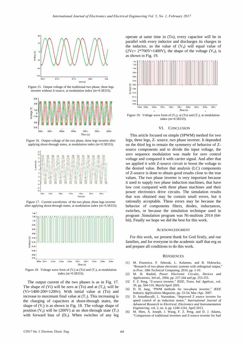
Figure 15. Output voltage of the traditional two phase, three legs inverter without Z-source, at modulation index (m=0.58333).
Figure 16. Output voltage of the two phase, three legs inverter after
applying shoot-through states, at modulation index (m=0.58333).
Figure 17. Current waveforms of the two phase ,three legs inverter after applying shoot-through states, at modulation index (m=0.58333).
Figure 18. Voltage wave form of (Vi) at (To) and (T1), at modulation index (m=0.58333).
The output current of the two phases is as in Fig. 17.
The shape of (Vi) will be zero at (To) and at (T1), will be
(Vi=1400-200=1200v). With initial value at (To) and
increase to maximum final value at (T1). This increasing is
the charging of capacitors at shoot-through states, the
shape of (Vi) is as shown in Fig. 18. The voltage shape of
position (Vd) will be (200V) at no shot-through state (T1)
with forward bias of (D1). When switches of any leg
operate at same time in (To), every capacitor will be in
parallel with every inductor and discharges its charges in
the inductor, so the value of (Vd) will equal value of
(2Vc= 2*700V=1400V), the shape of the voltage (Vd), is
as shown in Fig. 19.
Figure 19. Voltage wave form of (Vd), at (To) and (T1), at modulation index (m=0.58333).
VI. CONCLUSION
This article focused on simple (SPWM) method for two
legs, three legs, Z- source, two phase inverter. It depended
on the third leg to remain the symmetry of behavior of Z-
source components and to divide the input voltage, the
zero sequence modulation was made for zero control
voltage and compared it with carrier signal. And after that
we applied it with Z-source circuit to boost the voltage to
the desired value. Before that analysis (LC) components
of Z-source is done to obtain good results close to the true
values. The two phase inverter is very important because
it used to supply two phase induction machines, that have
low cost compared with three phase machines and their
power electronics drive circuits. The simulation results
that was obtained may be contain small errors, but it
rationally acceptable. These errors may be because the
behavior of components filters, diodes, inductances,
switches, or because the simulation technique used in
program .Simulation program was Ni-multism 2014 (64-
bit). Finally we hope we did the best for this work.
ACKNOWLEDGMENT
For this work, we present thank for God firstly, and our
families, and for everyone in the academic staff that erg us
and prepare all conditions to do this work.
REFERENCES
[1] M. Prazenica, P. Sekerak, L. Kalamen, and B. Dobrucku,
“Research of two phase electronic systems with orthogonal output,”
in Proc. 18th Technical Computing, 2010, pp. 1-10. [2] M. H. Rashid, Power Electronic Circuits, Devices and
Applications, 3rd ed., 2004, pp. 237-244 and pp. 253-255.
[3] F. Z. Peng, “Z-source inverter,” IEEE, Trans. Ind. Applicat., vol. 39, pp. 504-510, March/April 2003.
[4] D. H. Jang, “PWM methods for two-phase inverter,” IEEE
Industry Applications Magazine, pp. 53-54, Mar./Apr. 2007. [5] D. Amudhavalli, L. Narendran, “Improved Z source inverter for
speed control of an induction motor,” International Journal of
Advanced Research in Electrical, Electronics and Instrumentation Engineering, vol. 2, no. 4, pp. 1240-1241, April 2013.
[6] M. Shen, A. Joseph, J. Wang, F. Z. Peng, and D. J. Adams,
“Comparison of traditional inverters and Z-source inverter for fuel
International Journal of Electronics and Electrical Engineering Vol. 5, No. 1, February 2017
©2017 Int. J. Electron. Electr. Eng. 64

cell vehicles,” IEEE Transactions on Power Electronics, vol. 22,
no. 4, pp. 1453-1463, 2007.
[7] S. Rajakaruna and Y. R. L. Jayawickrama, “Designing impedance
network of z-source inverters,” in Proc. IEEE 7th International Power Engineering Conference, 2005, pp. 1-7.
[8] B. Y. Husodo, M. Anwari, S. M. Ayob, and Taufik, “Analysis and
simulation of Z-source inverter control methods,” in Proc. IPEC, 2010, pp. 699-704.
[9] P. J. Aswer and P. H. Zope, “Study and analysis of single phase Z-
source inverter,” International Journal of Research in Advent Technology, vol. 1, no. 5, December 2013.
[10] X. Li, Z. Yan, K. Pan, C. Ma, and H. Qi, “The control technology
research of the Z-source three phase four-bridge arm inverter,” Energy and Power Engineering, vol. 5, no. 4, pp. 733-735, 2013.
Ghassan A. Hameed completed his Bachelors in Electrical and
Electronics Engineering from Babil University in 2009. He worked in
control and power electronics laboratories for the same university from 2010 until 2014 and he is trying to complete his master in Electrical and
Electronic Engineering from University of Turkish Aeronautical
Association in Turkey now.
Mahmood N. Abed completed his Bachelors in Electrical Power
Engineering from The Technical College in Mosul in 2005. He worked
in power electronics, power system and transmission and distribution
laboratories in the same college along (2006-2010). He worked in Nineveh electrical distribution directorate from 2012 until 2014. He is
also trying to complete his master in Electrical and Electronic
Engineering from University of Turkish Aeronautical Association in Turkey now.
Ibrahim Mahariq took his B.Sc. degree from the department of
Electrical and Computer Engineering/ Palestine Polytechnic University
in 2003. He worked there as Teaching Assistant during 2003-2005. He received the M.Sc. in Design of Electrical Machines, and his Ph.D. in
Computational Electromagnetics from Middle East Technical
University, Ankara, Turkey. Mahariq was granted TUBITAK scholarship for his Ph.D. studies in 2010. Mahariq is currently working
on Photonics to earn his second Ph.D. in the department of Electrical
and Electronics Engineering at TOBB University of Economics and Technology, Ankara, Turkey. Mahariq is currently serving as an
Assistant Professor at the University of Turkish Aeronautical
Association, Department of Electrical and Electronics Engineering.
International Journal of Electronics and Electrical Engineering Vol. 5, No. 1, February 2017
©2017 Int. J. Electron. Electr. Eng. 65


![Real-Time Impedance-Based Stability Assessment of Grid ... · inverter impedances [3]. Stability is preserved if the inverter impedance is shaped to have a larger magnitude than grid](https://img.pdfslide.net/doc/110x75/5e7798422073b32df95c4f4e/real-time-impedance-based-stability-assessment-of-grid-inverter-impedances-3.jpg)