Embed Size (px)
Citation preview
© 2016 NXP B.V.
TWR-KL28Z User’s Guide
1. Introduction
The Tower development platform is a set of software
and hardware tools for evaluation and development. It is
an ideal tool for the rapid prototyping of
microcontroller-based applications.
The TWR-KL28Z supports power supply voltage range
from 1.71 V to 3.6 V. It features a KL28Z, a device
boasting a maximum operating frequency of 72 MHz,
up to 512 KB Flash and numerous analog and digital
peripherals.
The TWR-KL28Z includes the ARM open standard
embedded serial and debug adapter known as CMSIS-
DAP. This circuit offers the user several options for
serial communications, flash programming, and run-
control debugging.
The TWR-KL28Z microcontroller module is designed
to work either in standalone mode or as part of the
Tower System, a modular development platform that
enables rapid prototyping and tool re-use through
reconfigurable hardware.
NXP Semiconductors Document Number: TWRKL28ZUG
User's Guide Rev. 0 , 06/2016
Contents
1. Introduction .................................................................... 1 2. Getting Started ................................................................ 2 3. TWR-KL28Z Features ..................................................... 2 4. TWR-KL28Z Hardware Description ................................ 4
4.1. Power supply ........................................................ 4 4.2. Serial and debug adapter (OpenSDA) .................... 5 4.3. Microcontroller ..................................................... 6 4.4. Capacitive touch pad ............................................. 9 4.5. I2C Accelerometer Sensor ..................................... 9 4.6. LED ................................................................... 11 4.7. Analog reference voltage..................................... 11 4.8. Input/output headers............................................ 12
5. References .................................................................... 13 6. Revision History ........................................................... 13
TWR-KL28Z Features
TWR-KL28Z User’s Guide, Rev. 0, 06/2016
2 NXP Semiconductors
It can provide a broad range of expansion board options. The on-board interfaces include LED, a 3-axis
digital sensor (3D accelerometer), and two capacitive touch pads.
There are many software development tool options available to the user. Choices include Kinetis Design
Studio (KDS), IAR Embedded Workbench, Keil MDK featuring the µVision IDE, and so on.
All of these features combine to give users the Tower needed to rapidly prototype many embedded
designs: a powerful microcontroller built on a very low-power core and SOC platform, easy-access to
I/O with a large ecosystem of compatible hardware, a flexible programming and debug interface, and a
large ecosystem of software development environments.
2. Getting Started
Refer to the TWR-KL28Z Quick Start Package for step-by-step instructions for getting started with the
freedom board. See the “Jump Start Your Design” section at nxp.com/FREDEVPLA for the Quick Start
Package and software lab guides.
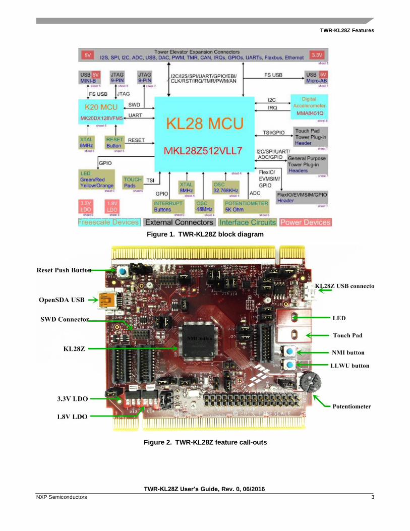
3. TWR-KL28Z Features
The TWR-KL28Z hardware is a Tower development board assembled with the following features:
• MKL28Z512VLL7 MCU (72 MHz, 512 KB Flash, 128 KB RAM, 32 KB ROM,100 LQFP
package)
• 3-Axis Digital Accelerometer, MMA8451Q
• On-board serial and debug adapter
• I/O headers for easy access to MCU I/O pins
• Flexible power supply options :USB, coin cell battery, external source
• Capacitive touch pad
• Reset push button
• NMI and LLWU buttons
• LEDs
The FRDM-KL28Z features two MCUs: The target MCU is the MKL28Z512VLL7. The CMSIS-DAP
MCU is the MK20DX128VFM5.
Figure 1 shows a block diagram of the TWR-KL28Z board. The primary components and their location
on the hardware assembly are pointed out in Figure 2.
TWR-KL28Z Features
TWR-KL28Z User’s Guide, Rev. 0, 06/2016
NXP Semiconductors 3
Figure 1. TWR-KL28Z block diagram
Figure 2. TWR-KL28Z feature call-outs
TWR-KL28Z Hardware Description
TWR-KL28Z User’s Guide, Rev. 0, 06/2016
4 NXP Semiconductors
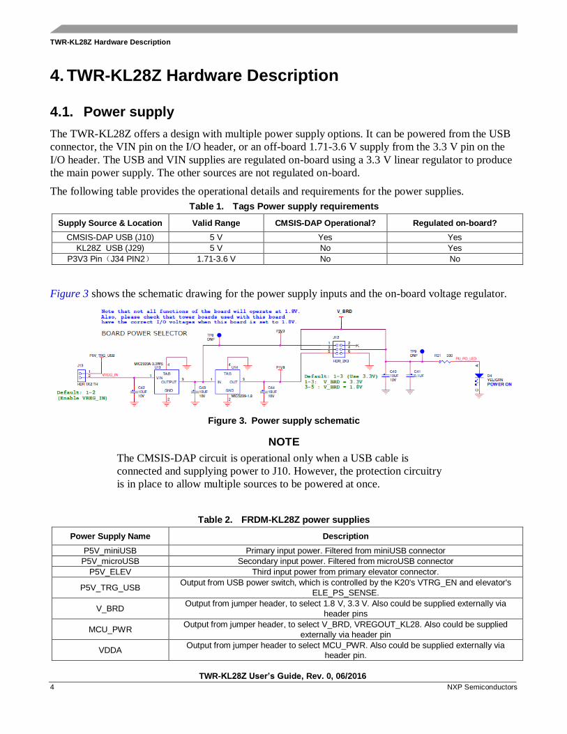
4. TWR-KL28Z Hardware Description
4.1. Power supply
The TWR-KL28Z offers a design with multiple power supply options. It can be powered from the USB
connector, the VIN pin on the I/O header, or an off-board 1.71-3.6 V supply from the 3.3 V pin on the
I/O header. The USB and VIN supplies are regulated on-board using a 3.3 V linear regulator to produce
the main power supply. The other sources are not regulated on-board.
The following table provides the operational details and requirements for the power supplies.
Table 1. Tags Power supply requirements
Supply Source & Location Valid Range CMSIS-DAP Operational? Regulated on-board?
CMSIS-DAP USB (J10) 5 V Yes Yes
KL28Z USB (J29) 5 V No Yes
P3V3 Pin(J34 PIN2) 1.71-3.6 V No No
Figure 3 shows the schematic drawing for the power supply inputs and the on-board voltage regulator.
Figure 3. Power supply schematic
NOTE
The CMSIS-DAP circuit is operational only when a USB cable is
connected and supplying power to J10. However, the protection circuitry
is in place to allow multiple sources to be powered at once.
Table 2. FRDM-KL28Z power supplies
Power Supply Name Description
P5V_miniUSB Primary input power. Filtered from miniUSB connector
P5V_microUSB Secondary input power. Filtered from microUSB connector
P5V_ELEV Third input power from primary elevator connector.
P5V_TRG_USB Output from USB power switch, which is controlled by the K20's VTRG_EN and elevator's
ELE_PS_SENSE.
V_BRD Output from jumper header, to select 1.8 V, 3.3 V. Also could be supplied externally via
header pins
MCU_PWR Output from jumper header, to select V_BRD, VREGOUT_KL28. Also could be supplied
externally via header pin
VDDA Output from jumper header to select MCU_PWR. Also could be supplied externally via
header pin.
TWR-KL28Z Hardware Description
TWR-KL28Z User’s Guide, Rev. 0, 06/2016
NXP Semiconductors 5
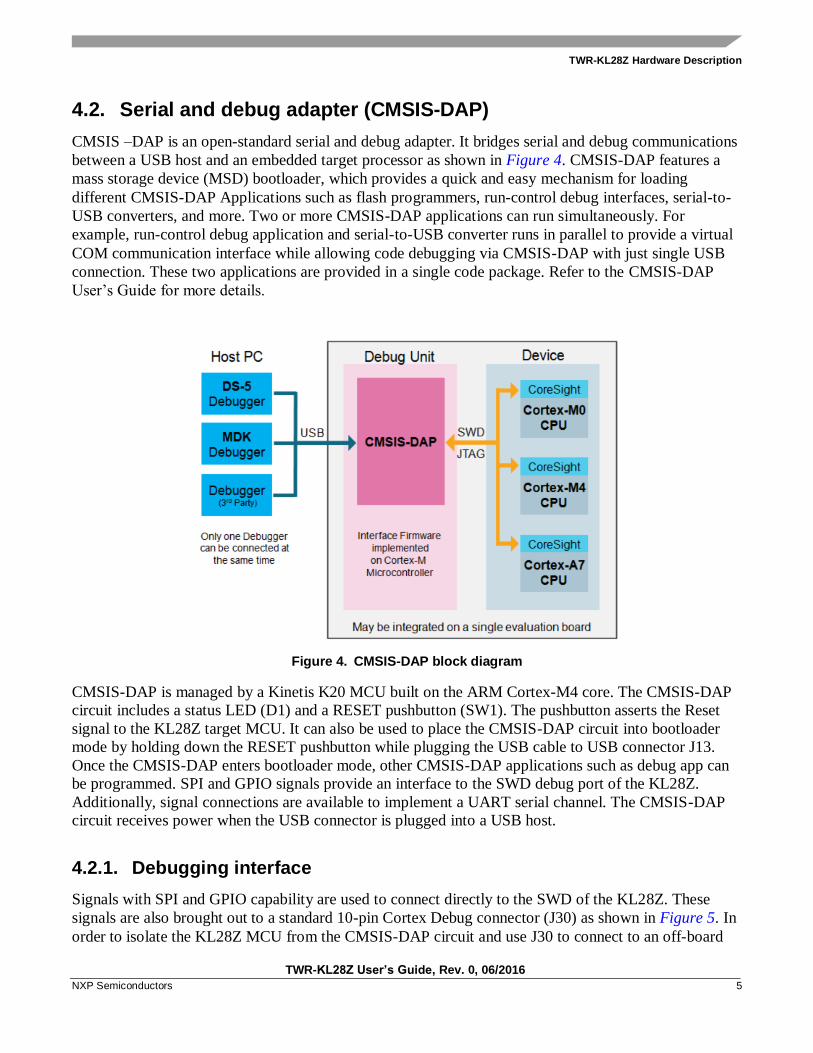
4.2. Serial and debug adapter (CMSIS-DAP)
CMSIS –DAP is an open-standard serial and debug adapter. It bridges serial and debug communications
between a USB host and an embedded target processor as shown in Figure 4. CMSIS-DAP features a
mass storage device (MSD) bootloader, which provides a quick and easy mechanism for loading
different CMSIS-DAP Applications such as flash programmers, run-control debug interfaces, serial-to-
USB converters, and more. Two or more CMSIS-DAP applications can run simultaneously. For
example, run-control debug application and serial-to-USB converter runs in parallel to provide a virtual
COM communication interface while allowing code debugging via CMSIS-DAP with just single USB
connection. These two applications are provided in a single code package. Refer to the CMSIS-DAP
User’s Guide for more details.
Figure 4. CMSIS-DAP block diagram
CMSIS-DAP is managed by a Kinetis K20 MCU built on the ARM Cortex-M4 core. The CMSIS-DAP
circuit includes a status LED (D1) and a RESET pushbutton (SW1). The pushbutton asserts the Reset
signal to the KL28Z target MCU. It can also be used to place the CMSIS-DAP circuit into bootloader
mode by holding down the RESET pushbutton while plugging the USB cable to USB connector J13.
Once the CMSIS-DAP enters bootloader mode, other CMSIS-DAP applications such as debug app can
be programmed. SPI and GPIO signals provide an interface to the SWD debug port of the KL28Z.
Additionally, signal connections are available to implement a UART serial channel. The CMSIS-DAP
circuit receives power when the USB connector is plugged into a USB host.
4.2.1. Debugging interface
Signals with SPI and GPIO capability are used to connect directly to the SWD of the KL28Z. These
signals are also brought out to a standard 10-pin Cortex Debug connector (J30) as shown in Figure 5. In
order to isolate the KL28Z MCU from the CMSIS-DAP circuit and use J30 to connect to an off-board
TWR-KL28Z Hardware Description
TWR-KL28Z User’s Guide, Rev. 0, 06/2016
6 NXP Semiconductors
MCU, cut the jumper between pin1 and pin2 of J32/J33 on bottom layer. This will disconnect the
SWD_CLK pin to the KL28Z so that it will interfere with the communications to an off-board MCU
connected to J30. Figure 5 shows SWD connector signals description for KL28Z.
Figure 5. SWD debug connector to KL28Z
4.2.2. Virtual serial port
A serial port connection is available between the CMSIS-DAP MCU and pins PTA1 and PTA2 of the
KL28Z. Several of the default CMSIS-DAP applications are provided by NXP, including the MSD
Flash Programmer and the CMSIS-DAP USB HID interface, providing a USB communications device
class (CDC) interface that bridges serial communications between the USB host and this serial interface.
4.3. Microcontroller
The TWR-KL28Z is a MCU module featuring the MKL28Z512VLL7, a Kinetis microcontroller with
USB 2.0 full-speed OTG controller in a 100 LQFP package. An on-board debug circuit, CMSIS-DAP,
provides a SWD interface and a power supply input through a mini-USB connector, as well as serial to
USB and CDC class compliant UART interface.
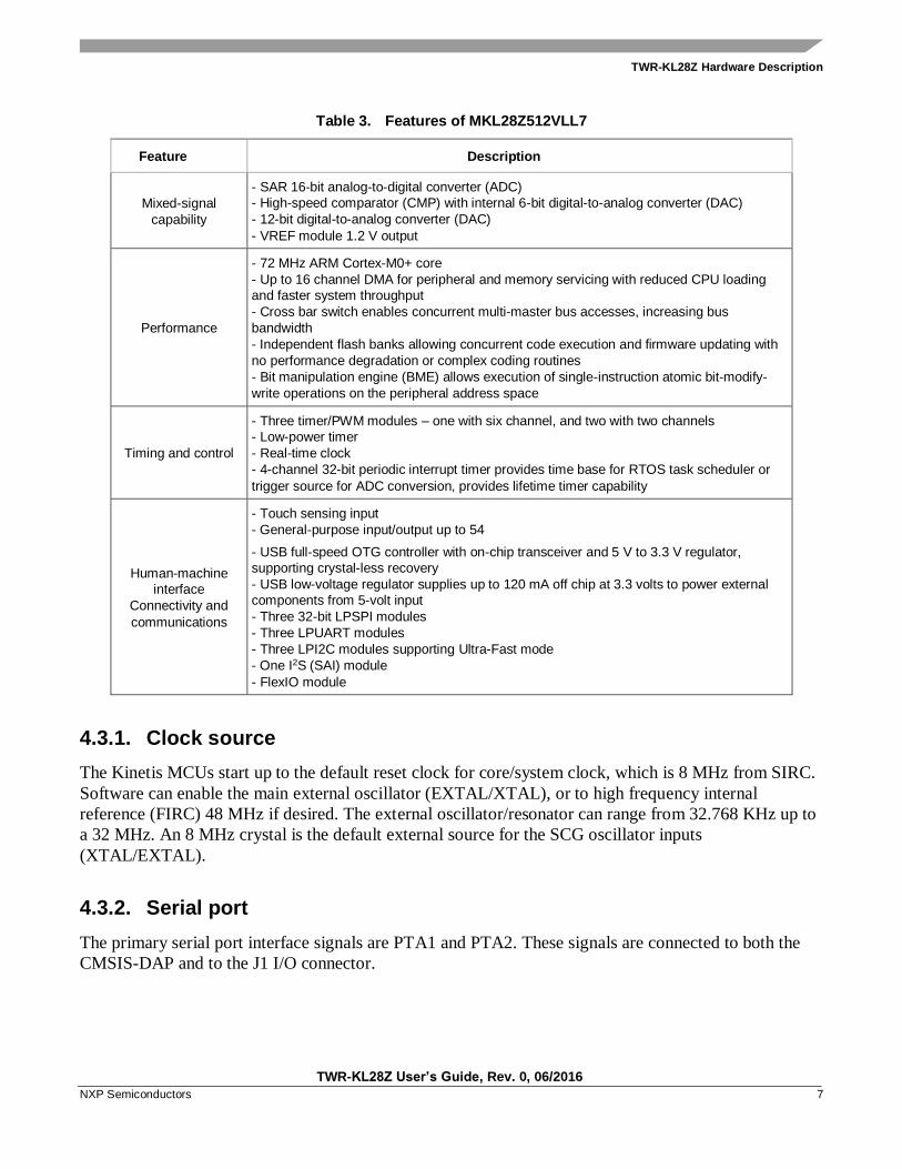
Table 3. Features of MKL28Z512VLL7
Feature Description
Ultra-low-power
- 10 low-power modes with power and clock gating for optimal peripheral activity and
recovery times. Stop currents of <190 nA (VLLS0), run currents of <280 uA/MHz, 4 s wake-
up from Stop mode
- Full memory and analog operation down to 1.71 V for extended battery life
- Low-leakage wake-up unit with up to eight internal modules and eight pins as wake-up
sources in low-leakage stop (LLS)/very low-leakage stop (VLLS) modes
- Low-power timer for continual system operation in reduced power states
Flash, SRAM, ROM
- 512 KB flash featuring fast access times, high reliability, and four levels of security
protection. No user or system intervention to complete programming and erase functions
and full operation down to 1.71 V
- 128 KB of SRAM
- 32 KB of ROM with Kinetis bootloader included (UART, SPI, I2C, USB-HID)
TWR-KL28Z Hardware Description
TWR-KL28Z User’s Guide, Rev. 0, 06/2016
NXP Semiconductors 7
Table 3. Features of MKL28Z512VLL7
Feature Description
Mixed-signal
capability
- SAR 16-bit analog-to-digital converter (ADC)
- High-speed comparator (CMP) with internal 6-bit digital-to-analog converter (DAC)
- 12-bit digital-to-analog converter (DAC)
- VREF module 1.2 V output
Performance
- 72 MHz ARM Cortex-M0+ core
- Up to 16 channel DMA for peripheral and memory servicing with reduced CPU loading
and faster system throughput
- Cross bar switch enables concurrent multi-master bus accesses, increasing bus
bandwidth
- Independent flash banks allowing concurrent code execution and firmware updating with
no performance degradation or complex coding routines
- Bit manipulation engine (BME) allows execution of single-instruction atomic bit-modify-
write operations on the peripheral address space
Timing and control
- Three timer/PWM modules – one with six channel, and two with two channels
- Low-power timer
- Real-time clock
- 4-channel 32-bit periodic interrupt timer provides time base for RTOS task scheduler or
trigger source for ADC conversion, provides lifetime timer capability
Human-machine
interface
Connectivity and
communications
- Touch sensing input
- General-purpose input/output up to 54
- USB full-speed OTG controller with on-chip transceiver and 5 V to 3.3 V regulator,
supporting crystal-less recovery
- USB low-voltage regulator supplies up to 120 mA off chip at 3.3 volts to power external
components from 5-volt input
- Three 32-bit LPSPI modules
- Three LPUART modules
- Three LPI2C modules supporting Ultra-Fast mode
- One I2S (SAI) module
- FlexIO module
4.3.1. Clock source
The Kinetis MCUs start up to the default reset clock for core/system clock, which is 8 MHz from SIRC.
Software can enable the main external oscillator (EXTAL/XTAL), or to high frequency internal
reference (FIRC) 48 MHz if desired. The external oscillator/resonator can range from 32.768 KHz up to
a 32 MHz. An 8 MHz crystal is the default external source for the SCG oscillator inputs
(XTAL/EXTAL).
4.3.2. Serial port
The primary serial port interface signals are PTA1 and PTA2. These signals are connected to both the
CMSIS-DAP and to the J1 I/O connector.
TWR-KL28Z Hardware Description
TWR-KL28Z User’s Guide, Rev. 0, 06/2016
8 NXP Semiconductors
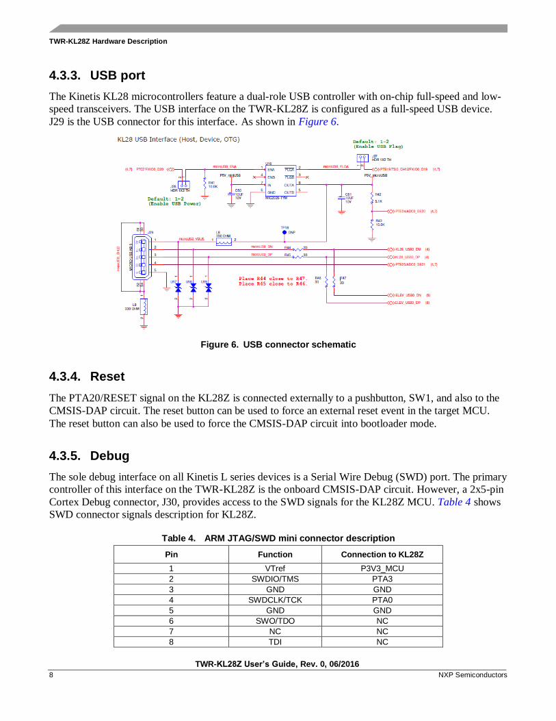
4.3.3. USB port
The Kinetis KL28 microcontrollers feature a dual-role USB controller with on-chip full-speed and low-
speed transceivers. The USB interface on the TWR-KL28Z is configured as a full-speed USB device.
J29 is the USB connector for this interface. As shown in Figure 6.
Figure 6. USB connector schematic
4.3.4. Reset
The PTA20/RESET signal on the KL28Z is connected externally to a pushbutton, SW1, and also to the
CMSIS-DAP circuit. The reset button can be used to force an external reset event in the target MCU.
The reset button can also be used to force the CMSIS-DAP circuit into bootloader mode.
4.3.5. Debug
The sole debug interface on all Kinetis L series devices is a Serial Wire Debug (SWD) port. The primary
controller of this interface on the TWR-KL28Z is the onboard CMSIS-DAP circuit. However, a 2x5-pin
Cortex Debug connector, J30, provides access to the SWD signals for the KL28Z MCU. Table 4 shows
SWD connector signals description for KL28Z.
Table 4. ARM JTAG/SWD mini connector description
Pin Function Connection to KL28Z
1 VTref P3V3_MCU
2 SWDIO/TMS PTA3
3 GND GND
4 SWDCLK/TCK PTA0
5 GND GND
6 SWO/TDO NC
7 NC NC
8 TDI NC
TWR-KL28Z Hardware Description
TWR-KL28Z User’s Guide, Rev. 0, 06/2016
NXP Semiconductors 9
Table 4. ARM JTAG/SWD mini connector description
Pin Function Connection to KL28Z
9 TDI NC
10 RESET PTA20
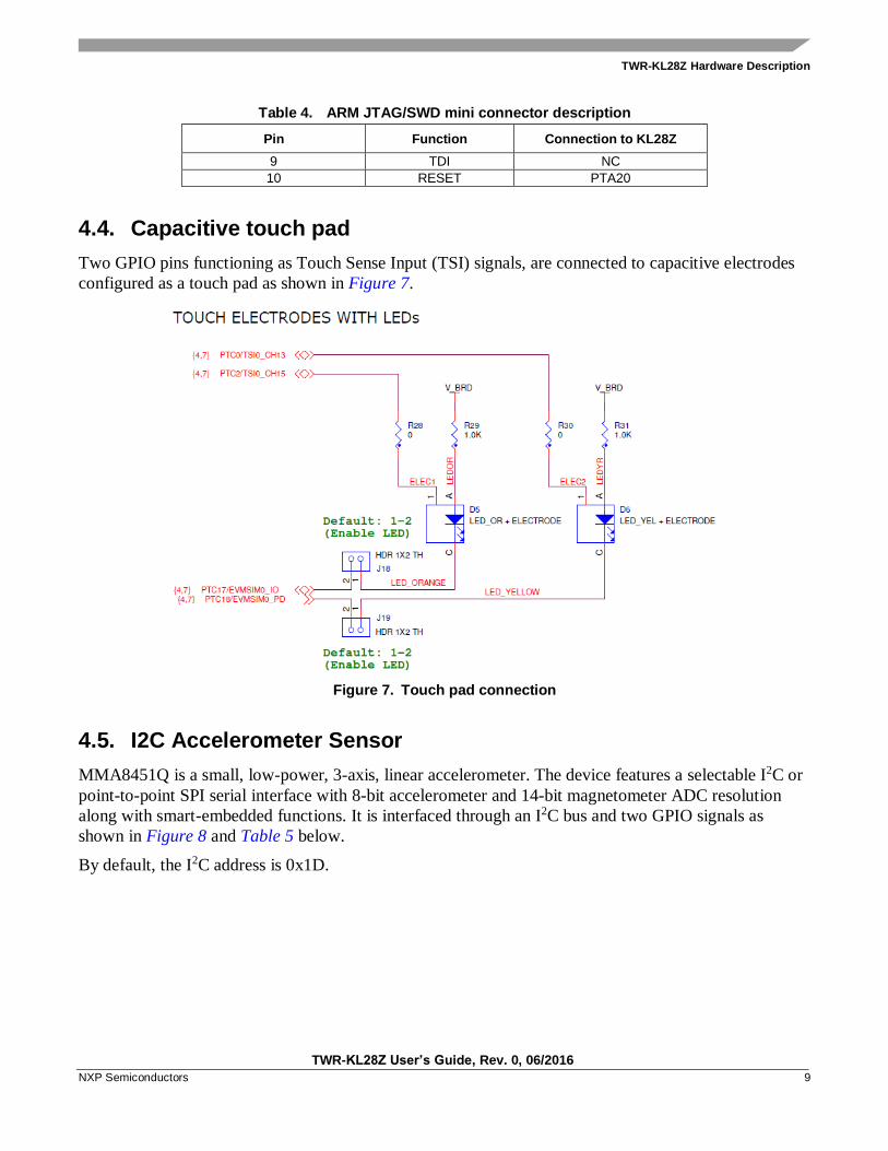
4.4. Capacitive touch pad
Two GPIO pins functioning as Touch Sense Input (TSI) signals, are connected to capacitive electrodes
configured as a touch pad as shown in Figure 7.
Figure 7. Touch pad connection
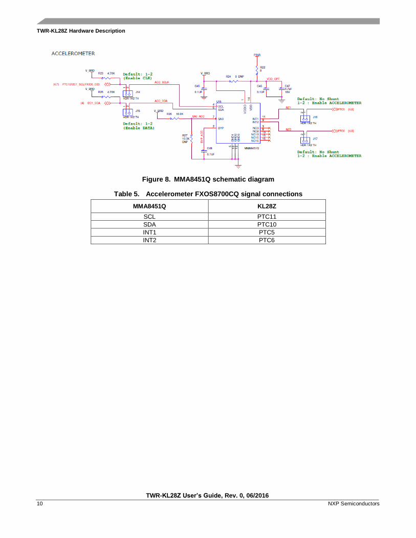
4.5. I2C Accelerometer Sensor
MMA8451Q is a small, low-power, 3-axis, linear accelerometer. The device features a selectable I2C or
point-to-point SPI serial interface with 8-bit accelerometer and 14-bit magnetometer ADC resolution
along with smart-embedded functions. It is interfaced through an I2C bus and two GPIO signals as
shown in Figure 8 and Table 5 below.
By default, the I2C address is 0x1D.
TWR-KL28Z Hardware Description
TWR-KL28Z User’s Guide, Rev. 0, 06/2016
10 NXP Semiconductors
Figure 8. MMA8451Q schematic diagram
Table 5. Accelerometer FXOS8700CQ signal connections
MMA8451Q KL28Z
SCL PTC11
SDA PTC10
INT1 PTC5
INT2 PTC6
TWR-KL28Z Hardware Description
TWR-KL28Z User’s Guide, Rev. 0, 06/2016
NXP Semiconductors 11
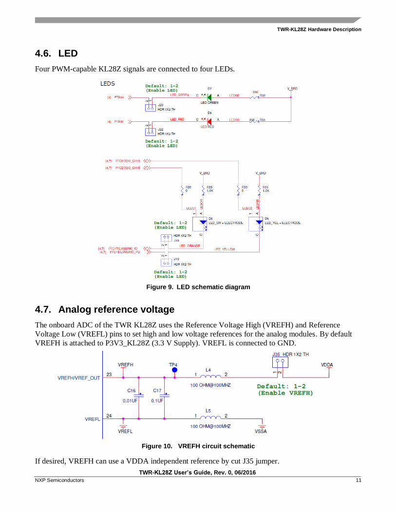
4.6. LED
Four PWM-capable KL28Z signals are connected to four LEDs.
Figure 9. LED schematic diagram
4.7. Analog reference voltage
The onboard ADC of the TWR KL28Z uses the Reference Voltage High (VREFH) and Reference
Voltage Low (VREFL) pins to set high and low voltage references for the analog modules. By default
VREFH is attached to P3V3_KL28Z (3.3 V Supply). VREFL is connected to GND.
Figure 10. VREFH circuit schematic
If desired, VREFH can use a VDDA independent reference by cut J35 jumper.
TWR-KL28Z Hardware Description
TWR-KL28Z User’s Guide, Rev. 0, 06/2016
12 NXP Semiconductors
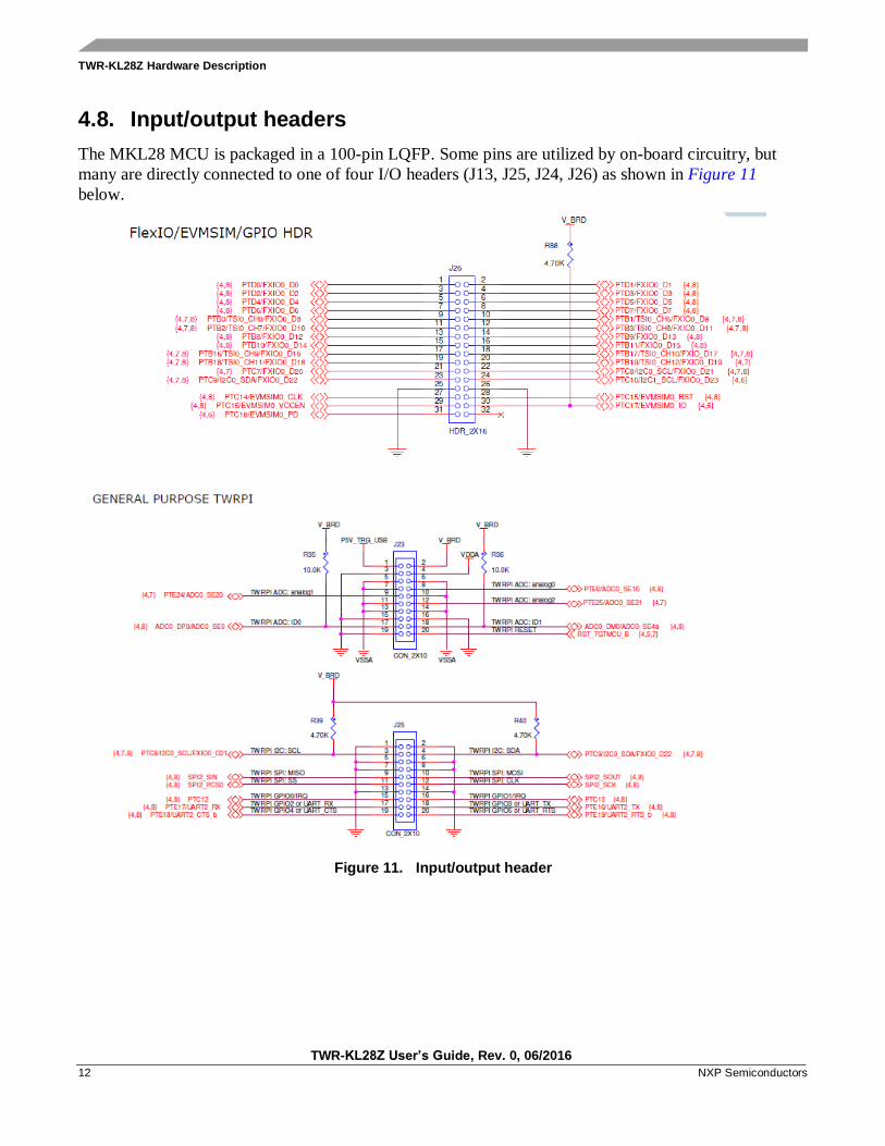
4.8. Input/output headers
The MKL28 MCU is packaged in a 100-pin LQFP. Some pins are utilized by on-board circuitry, but
many are directly connected to one of four I/O headers (J13, J25, J24, J26) as shown in Figure 11
below.
Figure 11. Input/output header
Revision History
TWR-KL28Z User’s Guide, Rev. 0, 06/2016
NXP Semiconductors 13
5. References
The reference documents for the TWR-KL28Z hardware are shown below. All documents can be found
at nxp.com
• TWR-KL28Z Quick Start Guide
• TWR-KL28Z User’s Guide
• TWR-KL28Z Schematics PDF
• KL28 Sub-Family Reference Manual
6. Revision History Table 6. Revision history
Revision number Date Substantive changes
0 06/2016 Initial release
Document Number: TWRKL28ZUG Rev. 0
06/2016
How to Reach Us:
Home Page:
nxp.com
Web Support:
nxp.com/support
Information in this document is provided solely to enable system and software
implementers to use NXP products. There are no express or implied copyright licenses
granted hereunder to design or fabricate any integrated circuits based on the
information in this document. NXP reserves the right to make changes without further
notice to any products herein.
NXP makes no warranty, representation, or guarantee regarding the suitability of its
products for any particular purpose, nor does NXP assume any liability arising out of
the application or use of any product or circuit, and specifically disclaims any and all
liability, including without limitation consequential or incidental damages. “Typical”
parameters that may be provided in NXP data sheets and/or specifications can and do
vary in different applications, and actual performance may vary over time. All operating
parameters, including “typicals,” must be validated for each customer application by
customer’s technical experts. NXP does not convey any license under its patent rights
nor the rights of others. NXP sells products pursuant to standard terms and conditions
of sale, which can be found at the following address:
nxp.com/SalesTermsandConditions.
NXP, the NXP logo, NXP SECURE CONNECTIONS FOR A SMARTER WORLD, and
Kinetis, are trademarks of NXP B.V. All other product or service names are the property
of their respective owners.
ARM, the ARM powered logo, and Cortex are registered trademarks of ARM Limited (or
its subsidiaries) in the EU and/or elsewhere. All rights reserved.
© 2016 NXP B.V.