Embed Size (px)
Citation preview
APPLICATION NOTE
REJ05B1378-0100 Rev.1.00 Page 1 of 46Apr. 30, 2010
1. AbstractThis documents describes the UART version program downloader for the R8C/35C Group.
2. IntroductionThe application example described in this document applies to the following microcomputer (MCU) and parameter:
• MCU: R8C/35C Group• XIN clock frequency: 20 MHz
This application note can be used with other R8C Family MCUs which have the same special function registers (SFRs)as the above group. Check the manual for any modifications to functions. Careful evaluation is recommended beforeusing the program described in this application note.
REJ05B1378-0100Rev.1.00
Apr. 30, 2010
R8C/35C GroupUART Version Program Downloader
R8C/35C Group UART Version Program Downloader
REJ05B1378-0100 Rev.1.00 Page 2 of 46Apr. 30, 2010
3. Program Downloader Overview
3.1 Downloader Specifications• The system program (including program downloader process) is allocated to block 0.• The program downloader erases and writes mainly to user programs other than the user program in block
0.The program downloader ignores rewrite operations to block 0.• EW0 mode is used by the program downloader for rewriting the CPU.• In a reset start, the program downloader checks the state of port P1_5 and selects either to use the program
downloader or the user program. The program downloader operates when port P1_5 is high, and the user program operates when port P1_5 is low.
• The virtual fixed vector table is allocated to block 1 to use the fixed vector table interrupt in the user program. • UART0 clock asynchronous serial I/O (UART) is used to communicate with a programmer.• CMOS output is selected for the TXD0 pin.• The communication format is as follows:
Bit rate: approximately 9600 bps Transfer data length: 8 bitsStop bit: 1 bit Parity bit: None
• Refer to 4. Downloader Communication Protocol for the communication protocol.
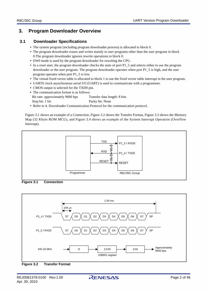
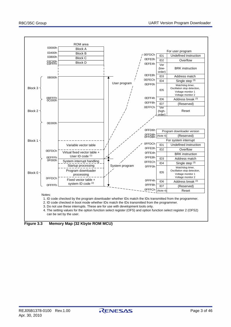
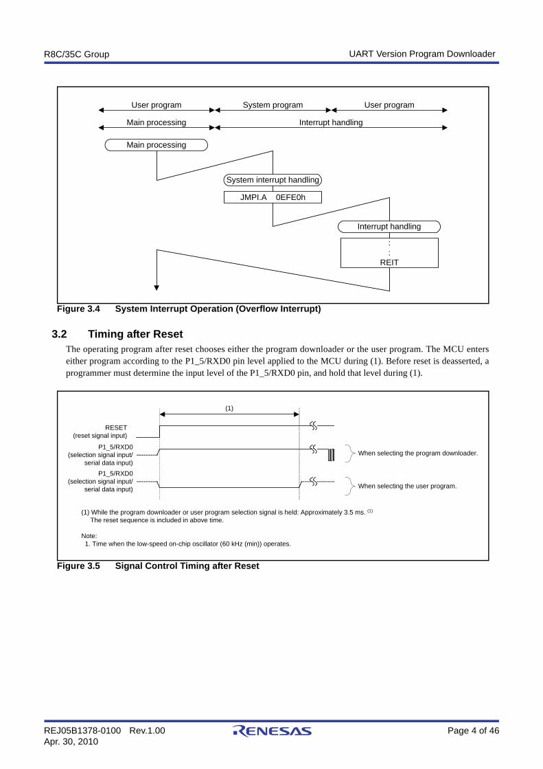
Figure 3.1 shows an example of a Connection, Figure 3.2 shows the Transfer Format, Figure 3.3 shows the MemoryMap (32 Kbyte ROM MCU), and Figure 3.4 shows an example of the System Interrupt Operation (OverflowInterrupt).
Figure 3.1 Connection
Figure 3.2 Transfer Format
RXD
TXD P1_5 / RXD0
P1_4 / TXD0
R8C/35C GroupProgrammer
RESET RESET
P1_4 / TXD0
P1_5 / RXD0
D0
D0
D1
D1
D2
D2
D3
D3
D4
D4
D5
D5
D6
D6
D7
D7
ST
ST
SP
SP
f1 1/129
U0BRG register
1/16 Approximately9600 bps
104 μs
1.04 ms
XIN 20 MHz
R8C/35C Group UART Version Program Downloader
REJ05B1378-0100 Rev.1.00 Page 3 of 46Apr. 30, 2010
Figure 3.3 Memory Map (32 Kbyte ROM MCU)
Program downloaderprocessing
ROM area
Fixed vector table +system ID code (2)
System interrupt handling
Virtual fixed vector table +User ID code (1)
0EFDCh
Startup processing
Variable vector table
Block ABlock B
Undefined instructionOverflow
Address matchSingle step (3)
Watchdog timer,Oscillation stop detection,
Voltage monitor 1Voltage monitor 2
Address break (3)
(Reserved)
Reset
ID1ID2
ID7
ID4
ID5
ID6
Ver(high-order)
BRK instruction
ID3
For user program
08000h
03400h
03000h
0EFFFh0F000h
0FFDCh
0FFFFh
Block 1
Block 0
0EFDCh0EFE0h
0EFE8h0EFECh0EFF0h
0EFF4h0EFF8h0EFFCh
0EFE4h
For system interrupt0FFDCh0FFE0h
0FFE8h0FFECh0FFF0h
0FFF4h0FFF8h0FFFCh
0FFE4h
Block CBlock D03FFFh
03C00h03800h
Block 2
Block 3
0BFFFh0C000h
0E000h
User program
System program
Undefined instructionOverflow
Address matchSingle step (3)
Watchdog timer,Oscillation stop detection,
Voltage monitor 1Voltage monitor 2
Address break (3)
(Reserved)Reset
ID1ID2
ID7
ID4
ID5
ID6
BRK instructionID3
Ver(low-order)
(Note 4)
0FFD6h Program downloader version(Reserved)(Note 4)0FFD8h
0FFDBh
Notes: 1. ID code checked by the program downloader whether IDs match the IDs transmitted from the programmer. 2. ID code checked in boot mode whether IDs match the IDs transmitted from the programmer. 3. Do not use these interrupts. These are for use with development tools only. 4. The setting values for the option function select register (OFS) and option function select register 2 (OFS2) can be set by the user.
R8C/35C Group UART Version Program Downloader
REJ05B1378-0100 Rev.1.00 Page 4 of 46Apr. 30, 2010
Figure 3.4 System Interrupt Operation (Overflow Interrupt)
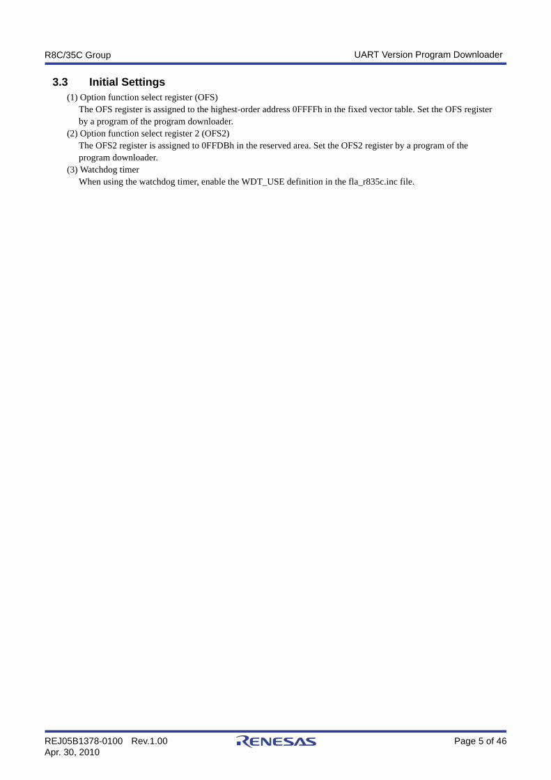
3.2 Timing after ResetThe operating program after reset chooses either the program downloader or the user program. The MCU enterseither program according to the P1_5/RXD0 pin level applied to the MCU during (1). Before reset is deasserted, aprogrammer must determine the input level of the P1_5/RXD0 pin, and hold that level during (1).
Figure 3.5 Signal Control Timing after Reset
Main processing
System interrupt handling
Interrupt handling
JMPI.A 0EFE0h
::
REIT
User program
Main processing
System program User program
Interrupt handling
RESET(reset signal input)
P1_5/RXD0(selection signal input/
serial data input)
(1) While the program downloader or user program selection signal is held: Approximately 3.5 ms. (1)
The reset sequence is included in above time.
Note: 1. Time when the low-speed on-chip oscillator (60 kHz (min)) operates.
(1)
P1_5/RXD0(selection signal input/
serial data input)
When selecting the program downloader.
When selecting the user program.
R8C/35C Group UART Version Program Downloader
REJ05B1378-0100 Rev.1.00 Page 5 of 46Apr. 30, 2010
3.3 Initial Settings(1) Option function select register (OFS)
The OFS register is assigned to the highest-order address 0FFFFh in the fixed vector table. Set the OFS register by a program of the program downloader.
(2) Option function select register 2 (OFS2)The OFS2 register is assigned to 0FFDBh in the reserved area. Set the OFS2 register by a program of the program downloader.
(3) Watchdog timerWhen using the watchdog timer, enable the WDT_USE definition in the fla_r835c.inc file.
R8C/35C Group UART Version Program Downloader
REJ05B1378-0100 Rev.1.00 Page 6 of 46Apr. 30, 2010
3.4 Registers
Port P1 Register P1 [address 00E1h]
0 0 0 1 0 0 0
UART0 Pin Select Register U0SR [address 0188h]
0 0 0 0 0 1 0 1
TXD0 pin select bit 1: P1_4 assigned
RXD0 pin select bit 1: P1_5 assigned
b7 b0
Port P1 Direction Register PD1 [address 00E3h]
0 0 0 1 0 0 0 0
Port P1_4 bit 1: High level
Port PD1_4 bit 1: Output mode (functions as TXD0 pin)
Port PD1_5 bit 0: Input mode (functions as RXD0 pin)
0
b7 b0
b7 b0
Watchdog Timer Reset Register WDTR [address 000Dh]
Writing 00h and then FFh to this register initializes thewatchdog timer.
0/1 0/1 0/1 0/1 0/1 0/1 0/1 0/1
b7 b0
Note: 1. This setting is unnecessary when the watchdog timer is not used.
Protect Register PRCR [address 000Ah]
0/1Enables writing to registers CM0, CM1, CM3, OCD, FRA0,FRA1, FRA2, and FRA3.0: Write disabled1: Write enabled
b7 b0
R8C/35C Group UART Version Program Downloader
REJ05B1378-0100 Rev.1.00 Page 7 of 46Apr. 30, 2010
System Clock Control Register 0 CM0 [address 0006h]
0 0
Oscillation Stop Detection Register OCD [address 000Ch]
0
System clock select bit0: XIN clock selected
XIN clock (XIN-XOUT) stop bit0: XIN clock oscillates
CPU clock division select bit 00: Bits CM16 and CM17 in CM1 register enabled
1: Divide-by-8 mode
XIN, XCIN clock select bit0: XIN clock
System Clock Control Register 1 CM1 [address 0007h]
0 0 0 1
Port/XIN-XOUT switch bit1: XIN-XOUT pin
Low-speed on-chip oscillator stop bit0: Low-speed on-chip oscillator on
CPU clock division select bit 10 0: No division mode
b7 b0
0/1
b7 b0
b7 b0
Interrupt Control Register S0TIC [address 0051h]
0 0 0 0 0 0 0
Interrupt priority level select bit 0 0 0: Level 0 (interrupt disabled)
0
b7 b0
Interrupt Control Register S0RIC [address 0052h]
0 0 0 0 0 0 0
Interrupt priority level select bit 0 0 0: Level 0 (interrupt disabled)
0
b7 b0
R8C/35C Group UART Version Program Downloader
REJ05B1378-0100 Rev.1.00 Page 8 of 46Apr. 30, 2010
UART0 Transmit/Receive Mode Register U0MR [address 00A0h]
0 0 0 0 0 1 0 1
UART0 Transmit/Receive Control Register 0 U0C0 [address 00A4h]
0 0 0 0 0 0 0
Data output select bit 0: TXD0 pin set to CMOS output
Internal/external clock select bit 0: Internal clock
Transfer format select bit 0: LSB first
b7 b0
b7 b0
Serial I/O mode select bit 101: UART mode, transfer data 8 bits long
Stop bit length select bit0: 1 stop bit
Odd/even parity select bitThis bit is not used. Set this bit to 0.
Parity enable bit0: Parity disabled
BRG count source select bit0 0: f1 selected
Set this bit to 0 in UART mode.
UART0 Transmit/Receive Control Register 1 U0C1 [address 00A5h]
0 0 0 1 0/1 0/1
Transmit enable bit 0: Transmission disabled 1: Transmission enabled
Receive enable bit0: Reception disabled
1: Reception enabled
Receive complete flag 0: No data in the U0RB register 1: Data present in the U0RB register
Set this bit to 0 in UART mode.
b7 b0
UART0 transmit interrupt source select bit1: Transmission completed (TXEPT = 1)
R8C/35C Group UART Version Program Downloader
REJ05B1378-0100 Rev.1.00 Page 9 of 46Apr. 30, 2010
UART0 Transmit Buffer Register U0TB [addresses 00A3h to 00A2h]
0/1 0/1 0/1 0/1 0/1 0/1 0/1
b7 b0
0/10 0 0 0 0 0 00
b15 b8
Transmit data
UART0 Receive Buffer Register U0RB [addresses 00A7h to 00A6h]
0
b7 b0b15 b8
Receive data
b7 b0
UART0 Bit Rate Register U0BRG [address 00A1h]
Bit rate setting Set to 129-1.
129-1
R8C/35C Group UART Version Program Downloader
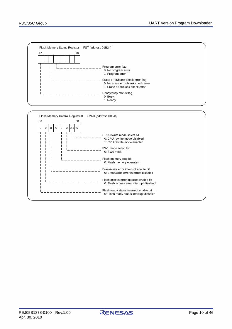
REJ05B1378-0100 Rev.1.00 Page 10 of 46Apr. 30, 2010
Flash Memory Control Register 0 FMR0 [address 01B4h]
0 0 0 0 0 0 0/1
CPU rewrite mode select bit0: CPU rewrite mode disabled1: CPU rewrite mode enabled
0
EW1 mode select bit0: EW0 mode
Flash memory stop bit0: Flash memory operates.
Erase/write error interrupt enable bit0: Erase/write error interrupt disabled
Flash access error interrupt enable bit0: Flash access error interrupt disabled
Flash ready status interrupt enable bit0: Flash ready status interrupt disabled
b7 b0
Flash Memory Status Register FST [address 01B2h]
Program error flag 0: No program error 1: Program error
Erase error/blank check error flag 0: No erase error/blank check error 1: Erase error/blank check error
Ready/busy status flag 0: Busy 1: Ready
b7 b0
R8C/35C Group UART Version Program Downloader
REJ05B1378-0100 Rev.1.00 Page 11 of 46Apr. 30, 2010
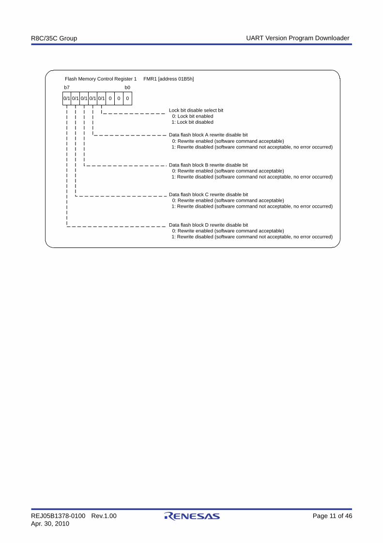
Flash Memory Control Register 1 FMR1 [address 01B5h]
0 0 0
Lock bit disable select bit0: Lock bit enabled
1: Lock bit disabled
0/1
Data flash block A rewrite disable bit0: Rewrite enabled (software command acceptable)
1: Rewrite disabled (software command not acceptable, no error occurred)
0/10/10/10/1
Data flash block B rewrite disable bit0: Rewrite enabled (software command acceptable)
1: Rewrite disabled (software command not acceptable, no error occurred)
Data flash block C rewrite disable bit0: Rewrite enabled (software command acceptable)
1: Rewrite disabled (software command not acceptable, no error occurred)
Data flash block D rewrite disable bit0: Rewrite enabled (software command acceptable)
1: Rewrite disabled (software command not acceptable, no error occurred)
b7 b0
R8C/35C Group UART Version Program Downloader
REJ05B1378-0100 Rev.1.00 Page 12 of 46Apr. 30, 2010
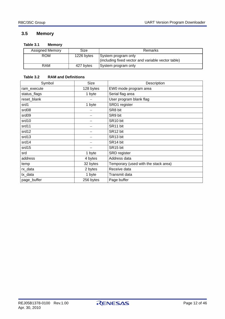
3.5 Memory
Table 3.2 RAM and Definitions
Table 3.1 MemoryAssigned Memory Size Remarks
ROM 1226 bytes System program only(including fixed vector and variable vector table)
RAM 427 bytes System program only
Symbol Size Descriptionram_execute 128 bytes EW0 mode program areastatus_flags 1 byte Serial flag areareset_blank − User program blank flagsrd1 1 byte SRD1 registersrd08 − SR8 bitsrd09 − SR9 bitsrd10 − SR10 bitsrd11 − SR11 bitsrd12 − SR12 bitsrd13 − SR13 bitsrd14 − SR14 bitsrd15 − SR15 bitsrd 1 byte SRD registeraddress 4 bytes Address datatemp 32 bytes Temporary (used with the stack area)rx_data 2 bytes Receive datatx_data 1 byte Transmit datapage_buffer 256 bytes Page buffer
R8C/35C Group UART Version Program Downloader
REJ05B1378-0100 Rev.1.00 Page 13 of 46Apr. 30, 2010
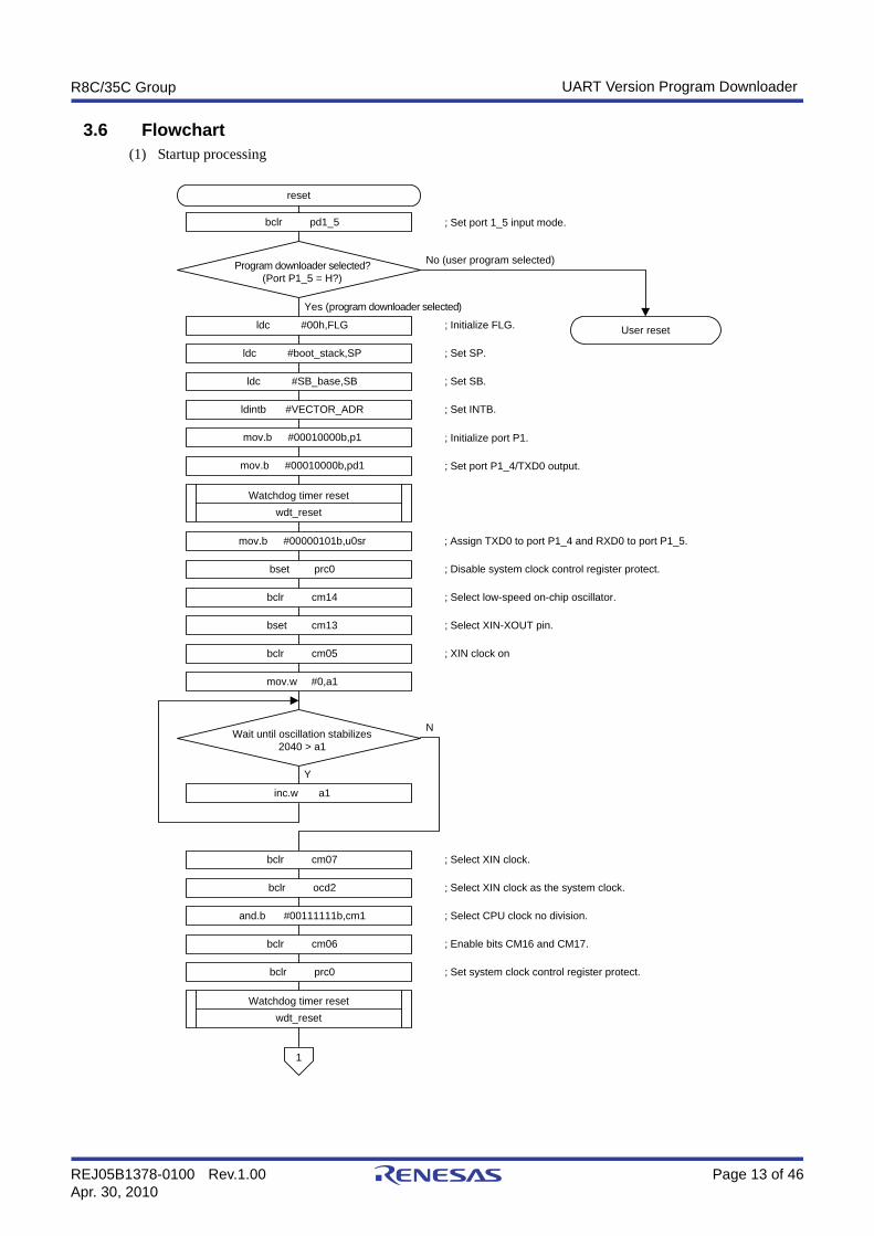
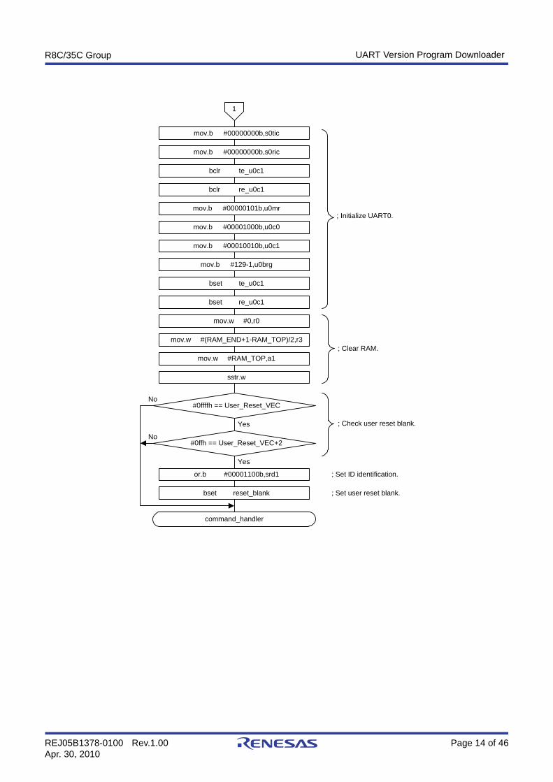
3.6 Flowchart(1) Startup processing
Program downloader selected?(Port P1_5 = H?)
No (user program selected)
Yes (program downloader selected)
ldc #boot_stack,SP
reset
User reset
ldc #SB_base,SB
ldintb #VECTOR_ADR
bset prc0
bset cm13
bclr cm05
bclr prc0
; Disable system clock control register protect.
; Set SP.
; Set SB.
; Set INTB.
; Select XIN-XOUT pin.
; XIN clock on
; Set system clock control register protect.
bclr cm14 ; Select low-speed on-chip oscillator.
ldc #00h,FLG ; Initialize FLG.
bclr pd1_5 ; Set port 1_5 input mode.
mov.b #00000101b,u0sr ; Assign TXD0 to port P1_4 and RXD0 to port P1_5.
Wait until oscillation stabilizes2040 > a1
Y
N
bclr cm07
bclr ocd2
and.b #00111111b,cm1
bclr cm06
; Select XIN clock.
; Select XIN clock as the system clock.
; Select CPU clock no division.
; Enable bits CM16 and CM17.
mov.b #00010000b,pd1
mov.b #00010000b,p1 ; Initialize port P1.
mov.w #0,a1
inc.w a1
1
; Set port P1_4/TXD0 output.
Watchdog timer resetwdt_reset
Watchdog timer resetwdt_reset
R8C/35C Group UART Version Program Downloader
REJ05B1378-0100 Rev.1.00 Page 14 of 46Apr. 30, 2010
command_handler
mov.b #00000101b,u0mr
mov.b #00001000b,u0c0
mov.b #00010010b,u0c1
bset re_u0c1
mov.w #0,r0
mov.w #(RAM_END+1-RAM_TOP)/2,r3
mov.w #RAM_TOP,a1
sstr.w
bset te_u0c1
mov.b #00000000b,s0ric
mov.b #00000000b,s0tic
#0ffffh == User_Reset_VECNo
Yes
#0ffh == User_Reset_VEC+2No
Yes
or.b #00001100b,srd1
bset reset_blank
; Set ID identification.
; Set user reset blank.
1
bclr te_u0c1
bclr re_u0c1
mov.b #129-1,u0brg
; Initialize UART0.
; Clear RAM.
; Check user reset blank.
R8C/35C Group UART Version Program Downloader
REJ05B1378-0100 Rev.1.00 Page 15 of 46Apr. 30, 2010
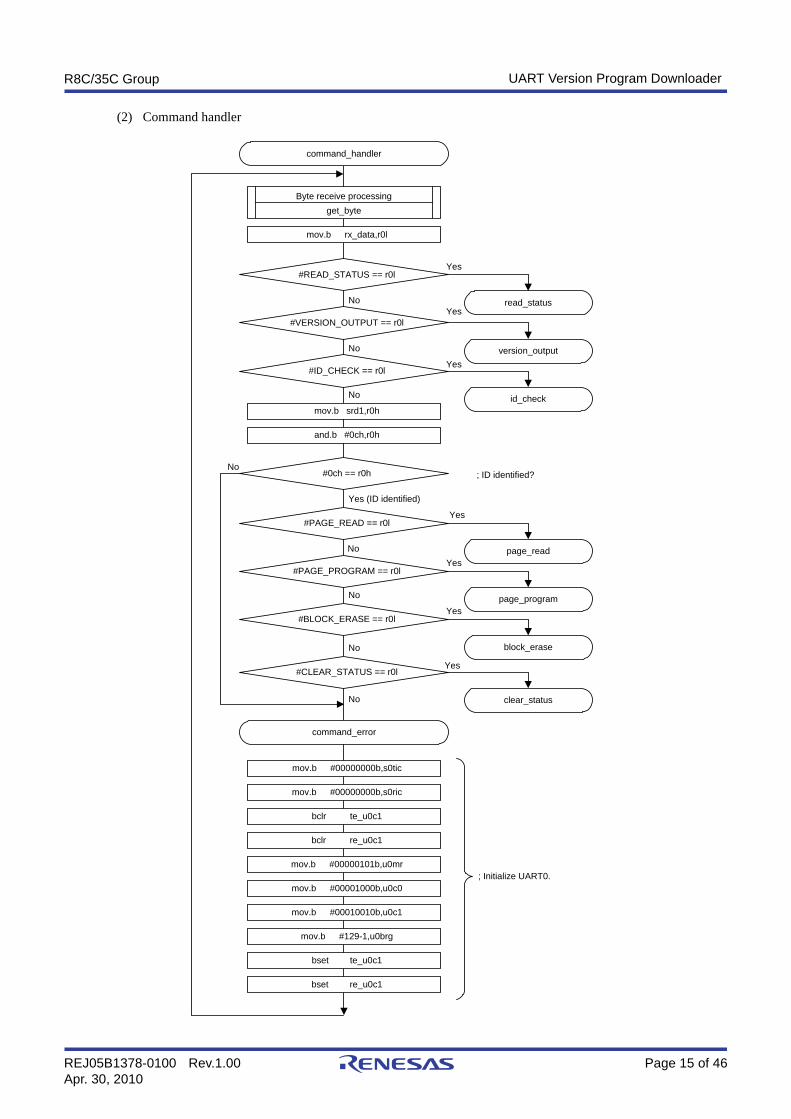
(2) Command handler
command_handler
read_status
mov.b #00000101b,u0mr
#READ_STATUS == r0l
command_error
mov.b rx_data,r0l
version_output
#VERSION_OUTPUT == r0l
id_check
#ID_CHECK == r0l
#0ch == r0h
Yes (ID identified)
mov.b srd1,r0h
and.b #0ch,r0h
page_read
#PAGE_READ == r0l
page_program
#PAGE_PROGRAM == r0l
block_erase
#BLOCK_ERASE == r0l
clear_status
#CLEAR_STATUS == r0l
mov.b #00001000b,u0c0
mov.b #00010010b,u0c1
bset re_u0c1
bset te_u0c1
mov.b #00000000b,s0ric
mov.b #00000000b,s0tic
Byte receive processingget_byte
; ID identified?
bclr re_u0c1
bclr te_u0c1
mov.b #129-1,u0brg
No
Yes
Yes
Yes
No
No
No
Yes
Yes
Yes
Yes
No
No
No
No
; Initialize UART0.
R8C/35C Group UART Version Program Downloader
REJ05B1378-0100 Rev.1.00 Page 16 of 46Apr. 30, 2010
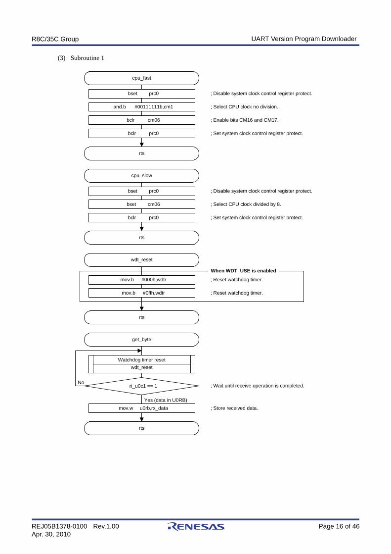
(3) Subroutine 1
cpu_fast
bset prc0
and.b #00111111b,cm1
bclr cm06
bclr prc0
ri_u0c1 == 1No
rts
cpu_slow
bset prc0
bset cm06
bclr prc0
rts
get_byte
mov.w u0rb,rx_data ; Store received data.
rts
; Wait until receive operation is completed.
; Disable system clock control register protect.
; Select CPU clock no division.
; Enable bits CM16 and CM17.
; Set system clock control register protect.
; Disable system clock control register protect.
; Select CPU clock divided by 8.
; Set system clock control register protect.
Yes (data in U0RB)
wdt_reset
mov.b #000h,wdtr
rts
mov.b #0ffh,wdtr
; Reset watchdog timer.
; Reset watchdog timer.
Watchdog timer resetwdt_reset
When WDT_USE is enabled
R8C/35C Group UART Version Program Downloader
REJ05B1378-0100 Rev.1.00 Page 17 of 46Apr. 30, 2010
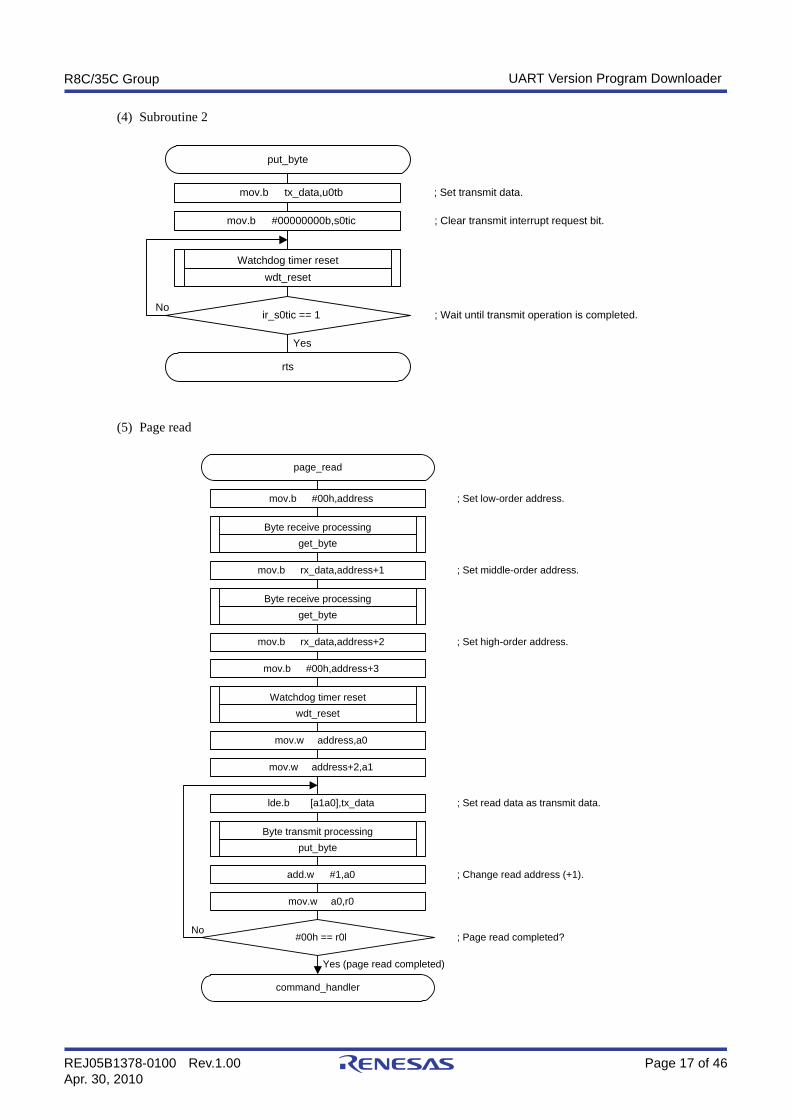
(4) Subroutine 2
(5) Page read
put_byte
mov.b tx_data,u0tb ; Set transmit data.
mov.b #00000000b,s0tic ; Clear transmit interrupt request bit.
ir_s0tic == 1No
; Wait until transmit operation is completed.
Yes
rts
Watchdog timer resetwdt_reset
page_read
mov.b #00h,address ; Set low-order address.
command_handler
Byte receive processingget_byte
#00h == r0lNo
Yes (page read completed)
mov.b rx_data,address+1 ; Set middle-order address.
mov.b rx_data,address+2 ; Set high-order address.
mov.b #00h,address+3
mov.w address,a0
mov.w address+2,a1
lde.b [a1a0],tx_data
Byte transmit processingput_byte
add.w #1,a0
mov.w a0,r0
; Page read completed?
; Set read data as transmit data.
; Change read address (+1).
Byte receive processingget_byte
Watchdog timer resetwdt_reset
R8C/35C Group UART Version Program Downloader
REJ05B1378-0100 Rev.1.00 Page 18 of 46Apr. 30, 2010
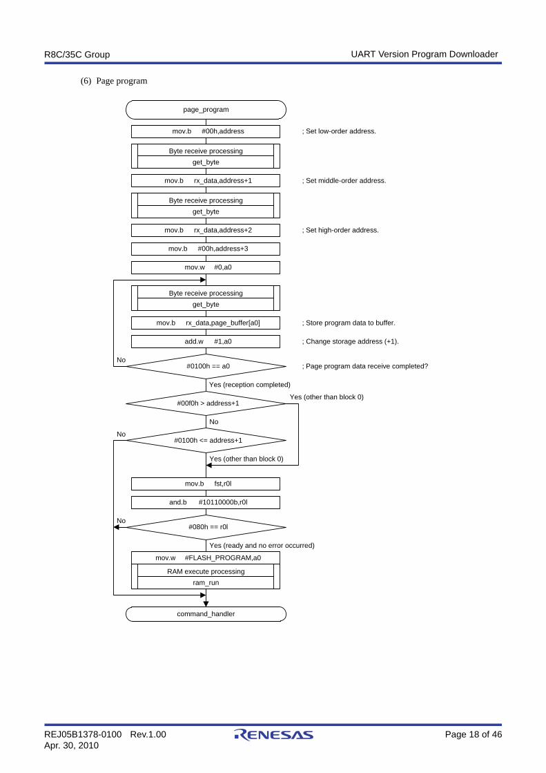
(6) Page program
page_program
mov.b #00h,address ; Set low-order address.
Byte receive processingget_byte
#0100h == a0
Yes (reception completed)
mov.b rx_data,address+1 ; Set middle-order address.
mov.b rx_data,address+2 ; Set high-order address.
mov.b #00h,address+3
mov.w #0,a0
add.w #1,a0
; Page program data receive completed?
; Change storage address (+1).
mov.b rx_data,page_buffer[a0] ; Store program data to buffer.
Byte receive processingget_byte
Byte receive processingget_byte
#00f0h > address+1
No
command_handler
mov.b fst,r0l
and.b #10110000b,r0l
#080h == r0l
#0100h <= address+1No
No
Yes (other than block 0)
No
Yes (ready and no error occurred)
RAM execute processingram_run
mov.w #FLASH_PROGRAM,a0
Yes (other than block 0)
R8C/35C Group UART Version Program Downloader
REJ05B1378-0100 Rev.1.00 Page 19 of 46Apr. 30, 2010
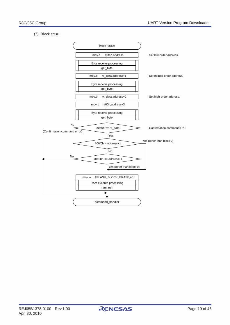
(7) Block erase
block_erase
mov.b #0feh,address ; Set low-order address.
command_handler
Byte receive processingget_byte
mov.b rx_data,address+1 ; Set middle-order address.
mov.b rx_data,address+2 ; Set high-order address.
mov.b #00h,address+3
RAM execute processingram_run
mov.w #FLASH_BLOCK_ERASE,a0
#0d0h == rx_data ; Confirmation command OK?
Byte receive processingget_byte
Byte receive processingget_byte
#00f0h > address+1
No
#0100h <= address+1No
Yes (other than block 0)
Yes (other than block 0)
Yes
No
(Confirmation command error)
R8C/35C Group UART Version Program Downloader
REJ05B1378-0100 Rev.1.00 Page 20 of 46Apr. 30, 2010
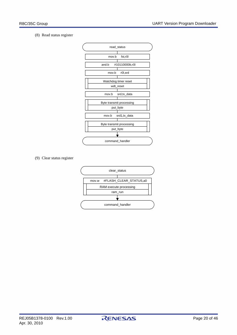
(8) Read status register
(9) Clear status register
read_status
command_handler
Byte transmit processingput_byte
mov.b srd,tx_data
mov.b srd1,tx_data
Byte transmit processingput_byte
mov.b fst,r0l
and.b #10110000b,r0l
mov.b r0l,srd
Watchdog timer resetwdt_reset
clear_status
command_handler
RAM execute processingram_run
mov.w #FLASH_CLEAR_STATUS,a0
R8C/35C Group UART Version Program Downloader
REJ05B1378-0100 Rev.1.00 Page 21 of 46Apr. 30, 2010
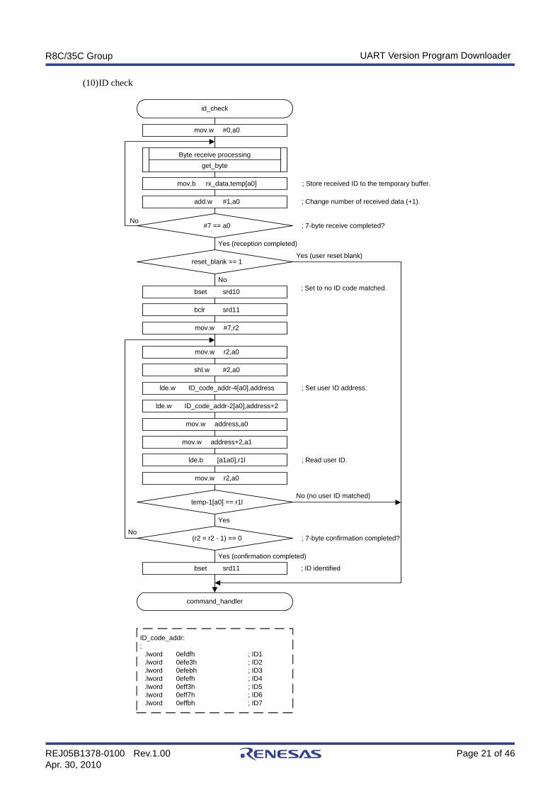
(10)ID check
id_check
command_handler
#7 == a0No
Yes (reception completed)
mov.w #0,a0
add.w #1,a0
; 7-byte receive completed?
; Change number of received data (+1).
Byte receive processingget_byte
mov.b rx_data,temp[a0]
reset_blank == 1Yes (user reset blank)
No
bset srd10
bclr srd11
mov.w #7,r2
temp-1[a0] == r1l
Yes
lde.w ID_code_addr-2[a0],address+2
; 7-byte confirmation completed?
; Set user ID address.lde.w ID_code_addr-4[a0],address
mov.w r2,a0
shl.w #2,a0
mov.w address+2,a1
mov.w address,a0
lde.b [a1a0],r1l ; Read user ID.
mov.w r2,a0
(r2 = r2 - 1) == 0No
Yes (confirmation completed)
No (no user ID matched)
bset srd11
ID_code_addr:;
.lword 0efdfh ; ID1
.lword 0efe3h ; ID2
.lword 0efebh ; ID3
.lword 0efefh ; ID4
.lword 0eff3h ; ID5
.lword 0eff7h ; ID6
.lword 0effbh ; ID7
; Store received ID to the temporary buffer.
; Set to no ID code matched.
; ID identified
R8C/35C Group UART Version Program Downloader
REJ05B1378-0100 Rev.1.00 Page 22 of 46Apr. 30, 2010
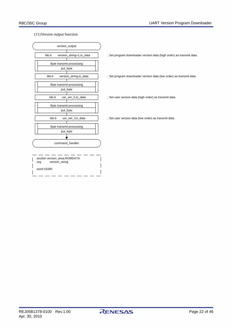
(11)Version output function
version_output
command_handler
Byte transmit processingput_byte
lde.b version_string+1,tx_data
lde.b usr_ver_l,tx_data
; Set program downloader version data (high order) as transmit data.
; Set user version data (low order) as transmit data.
.section version_area,ROMDATA
.org version_string
.word 0100h
Byte transmit processingput_byte
Byte transmit processingput_byte
lde.b version_string,tx_data ; Set program downloader version data (low order) as transmit data.
lde.b usr_ver_h,tx_data ; Set user version data (high order) as transmit data.
Byte transmit processingput_byte
R8C/35C Group UART Version Program Downloader
REJ05B1378-0100 Rev.1.00 Page 23 of 46Apr. 30, 2010
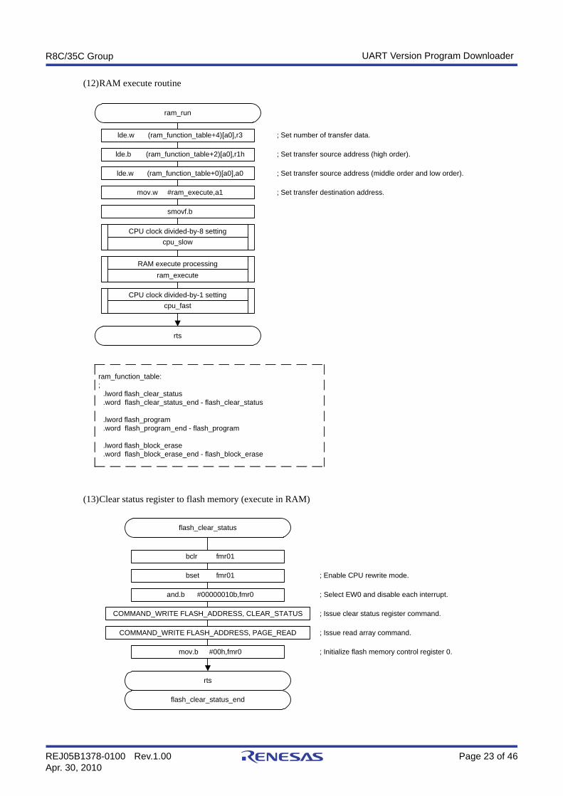
(12)RAM execute routine
(13)Clear status register to flash memory (execute in RAM)
ram_run
rts
CPU clock divided-by-8 settingcpu_slow
lde.w (ram_function_table+4)[a0],r3
CPU clock divided-by-1 settingcpu_fast
lde.b (ram_function_table+2)[a0],r1h
lde.w (ram_function_table+0)[a0],a0
; Set number of transfer data.
; Set transfer source address (high order).
; Set transfer source address (middle order and low order).
mov.w #ram_execute,a1 ; Set transfer destination address.
smovf.b
ram_function_table:;
.lword flash_clear_status
.word flash_clear_status_end - flash_clear_status
.lword flash_program
.word flash_program_end - flash_program
.lword flash_block_erase
.word flash_block_erase_end - flash_block_erase
RAM execute processingram_execute
flash_clear_status
rts
bclr fmr01
bset fmr01
and.b #00000010b,fmr0
; Enable CPU rewrite mode.
; Issue clear status register command.COMMAND_WRITE FLASH_ADDRESS, CLEAR_STATUS
; Issue read array command.COMMAND_WRITE FLASH_ADDRESS, PAGE_READ
mov.b #00h,fmr0 ; Initialize flash memory control register 0.
flash_clear_status_end
; Select EW0 and disable each interrupt.
R8C/35C Group UART Version Program Downloader
REJ05B1378-0100 Rev.1.00 Page 24 of 46Apr. 30, 2010
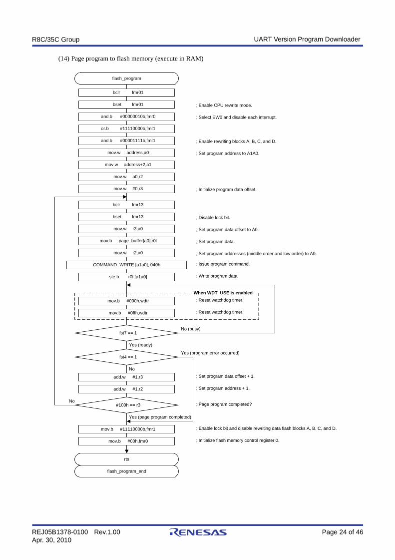
(14) Page program to flash memory (execute in RAM)
flash_program
rts
bclr fmr01
bset fmr01
and.b #00000010b,fmr0
; Enable CPU rewrite mode.
or.b #11110000b,fmr1
; Issue program command.COMMAND_WRITE [a1a0], 040h
ste.b r0l,[a1a0] ; Write program data.
mov.b #00h,fmr0 ; Initialize flash memory control register 0.
; Enable rewriting blocks A, B, C, and D.
flash_program_end
mov.w address,a0
mov.w address+2,a1
mov.w a0,r2
mov.w #0,r3
; Set program address to A1A0.
mov.w r3,a0
mov.b page_buffer[a0],r0l
mov.w r2,a0
add.w #1,r3 ; Set program data offset + 1.
add.w #1,r2 ; Set program address + 1.
#100h == r3
Yes (page program completed)
; Page program completed?
; Initialize program data offset.
; Set program addresses (middle order and low order) to A0.
; Set program data.
; Set program data offset to A0.
and.b #00001111b,fmr1
fst4 == 1
No
No
Yes (program error occurred)
bclr fmr13
bset fmr13 ; Disable lock bit.
mov.b #11110000b,fmr1 ; Enable lock bit and disable rewriting data flash blocks A, B, C, and D.
fst7 == 1
mov.b #000h,wdtr
mov.b #0ffh,wdtr
; Reset watchdog timer.
; Reset watchdog timer.
No (busy)
Yes (ready)
; Select EW0 and disable each interrupt.
When WDT_USE is enabled
R8C/35C Group UART Version Program Downloader
REJ05B1378-0100 Rev.1.00 Page 25 of 46Apr. 30, 2010
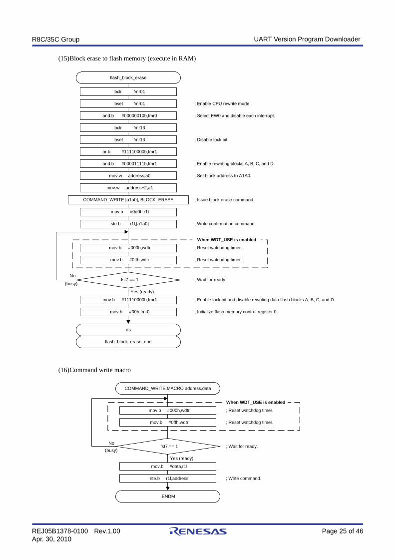
(15)Block erase to flash memory (execute in RAM)
(16)Command write macro
flash_block_erase
rts
bclr fmr01
bset fmr01
bclr fmr13
; Enable CPU rewrite mode.
bset fmr13
; Issue block erase command.COMMAND_WRITE [a1a0], BLOCK_ERASE
mov.b #0d0h,r1l
; Write confirmation command.
; Disable lock bit.
flash_block_erase_end
mov.w address,a0 ; Set block address to A1A0.
mov.w address+2,a1
ste.b r1l,[a1a0]
or.b #11110000b,fmr1
and.b #00001111b,fmr1 ; Enable rewriting blocks A, B, C, and D.
and.b #00000010b,fmr0
mov.b #00h,fmr0 ; Initialize flash memory control register 0.
mov.b #11110000b,fmr1 ; Enable lock bit and disable rewriting data flash blocks A, B, C, and D.
fst7 == 1
mov.b #000h,wdtr
mov.b #0ffh,wdtr
; Reset watchdog timer.
; Reset watchdog timer.
Yes (ready)
; Wait for ready.
; Select EW0 and disable each interrupt.
No
(busy)
When WDT_USE is enabled
COMMAND_WRITE.MACRO address,data
.ENDM
mov.b #000h,wdtr
mov.b #0ffh,wdtr
; Reset watchdog timer.
fst7 == 1
Yes (ready)
; Wait for ready.
mov.b #data,r1l
ste.b r1l,address ; Write command.
; Reset watchdog timer.
No(busy)
When WDT_USE is enabled
R8C/35C Group UART Version Program Downloader
REJ05B1378-0100 Rev.1.00 Page 26 of 46Apr. 30, 2010
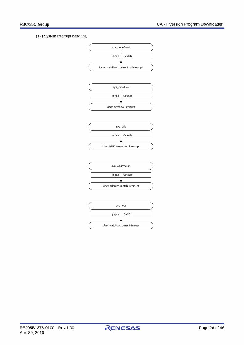
(17) System interrupt handling
sys_undefined
jmpi.a 0efdch
User undefined instruction interrupt
sys_overflow
jmpi.a 0efe0h
User overflow interrupt
sys_brk
jmpi.a 0efe4h
User BRK instruction interrupt
sys_addrmatch
jmpi.a 0efe8h
User address match interrupt
sys_wdt
jmpi.a 0eff0h
User watchdog timer interrupt
R8C/35C Group UART Version Program Downloader
REJ05B1378-0100 Rev.1.00 Page 27 of 46Apr. 30, 2010
4. Downloader Communication Protocol
4.1 Commands
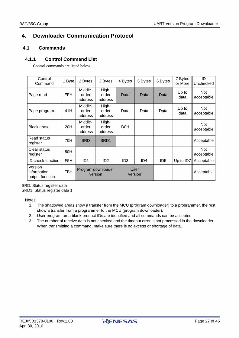
4.1.1 Control Command ListControl commands are listed below.
SRD: Status register dataSRD1: Status register data 1
Notes:1. The shadowed areas show a transfer from the MCU (program downloader) to a programmer, the rest
show a transfer from a programmer to the MCU (program downloader).2. User program area blank product IDs are identified and all commands can be accepted.3. The number of receive data is not checked and the timeout error is not processed in the downloader.
When transmitting a command, make sure there is no excess or shortage of data.
Control Command 1 Byte 2 Bytes 3 Bytes 4 Bytes 5 Bytes 6 Bytes 7 Bytes
or MoreID
Unchecked
Page read FFHMiddle-order
address
High-order
addressData Data Data Up to
dataNot
acceptable
Page program 41HMiddle-order
address
High-order
addressData Data Data Up to
dataNot
acceptable
Block erase 20HMiddle-order
address
High-order
addressD0H Not
acceptable
Read status register 70H SRD SRD1 Acceptable
Clear status register 50H Not
acceptableID check function F5H ID1 ID2 ID3 ID4 ID5 Up to ID7 AcceptableVersion information output function
FBH Program downloader version
User version Acceptable
R8C/35C Group UART Version Program Downloader
REJ05B1378-0100 Rev.1.00 Page 28 of 46Apr. 30, 2010
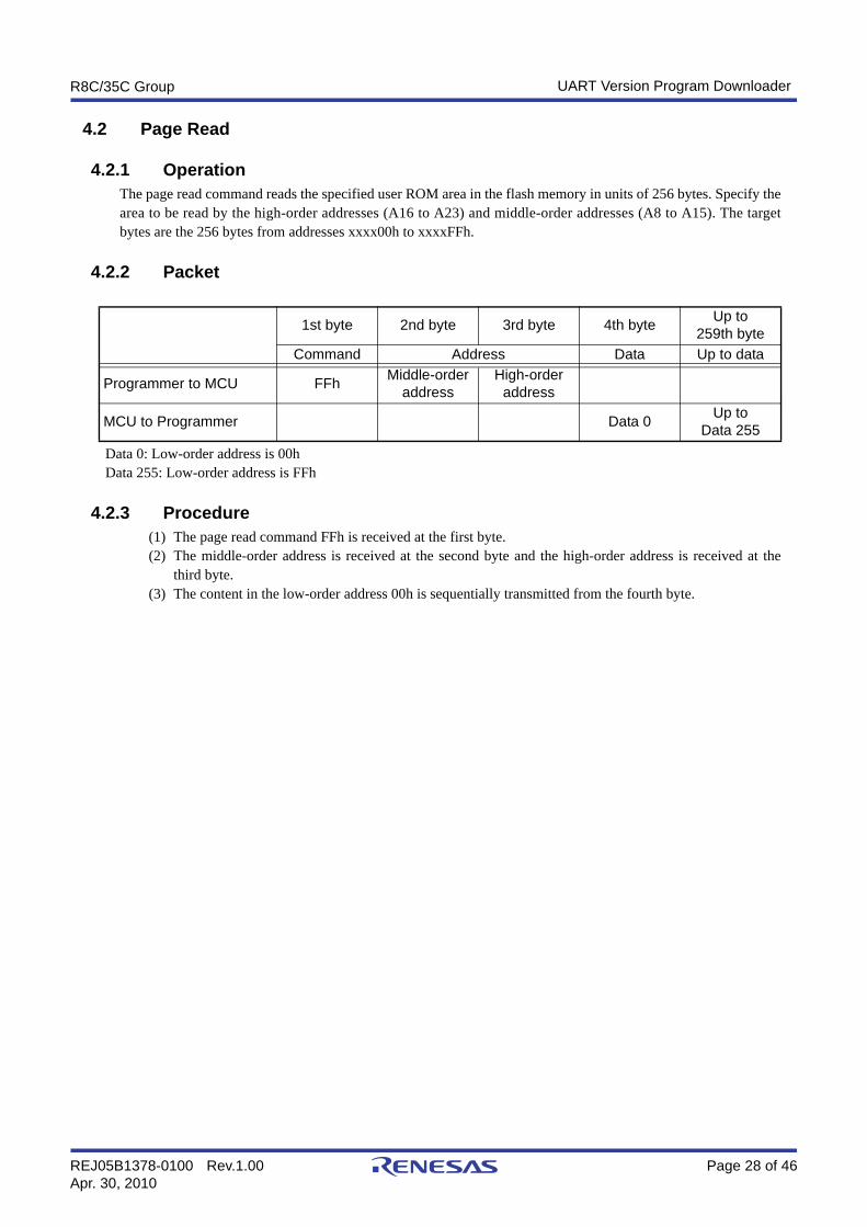
4.2 Page Read
4.2.1 OperationThe page read command reads the specified user ROM area in the flash memory in units of 256 bytes. Specify thearea to be read by the high-order addresses (A16 to A23) and middle-order addresses (A8 to A15). The targetbytes are the 256 bytes from addresses xxxx00h to xxxxFFh.
4.2.2 Packet
Data 0: Low-order address is 00hData 255: Low-order address is FFh
4.2.3 Procedure(1) The page read command FFh is received at the first byte.(2) The middle-order address is received at the second byte and the high-order address is received at the
third byte. (3) The content in the low-order address 00h is sequentially transmitted from the fourth byte.
1st byte 2nd byte 3rd byte 4th byte Up to 259th byte
Command Address Data Up to data
Programmer to MCU FFh Middle-order address
High-orderaddress
MCU to Programmer Data 0 Up to Data 255
R8C/35C Group UART Version Program Downloader
REJ05B1378-0100 Rev.1.00 Page 29 of 46Apr. 30, 2010
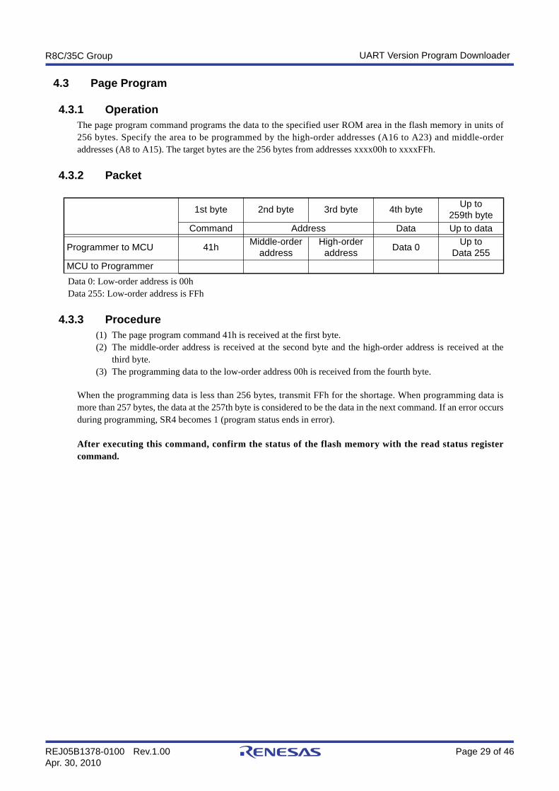
4.3 Page Program
4.3.1 OperationThe page program command programs the data to the specified user ROM area in the flash memory in units of256 bytes. Specify the area to be programmed by the high-order addresses (A16 to A23) and middle-orderaddresses (A8 to A15). The target bytes are the 256 bytes from addresses xxxx00h to xxxxFFh.
4.3.2 Packet
Data 0: Low-order address is 00hData 255: Low-order address is FFh
4.3.3 Procedure(1) The page program command 41h is received at the first byte.(2) The middle-order address is received at the second byte and the high-order address is received at the
third byte.(3) The programming data to the low-order address 00h is received from the fourth byte.
When the programming data is less than 256 bytes, transmit FFh for the shortage. When programming data ismore than 257 bytes, the data at the 257th byte is considered to be the data in the next command. If an error occursduring programming, SR4 becomes 1 (program status ends in error).
After executing this command, confirm the status of the flash memory with the read status registercommand.
1st byte 2nd byte 3rd byte 4th byte Up to 259th byte
Command Address Data Up to data
Programmer to MCU 41h Middle-order address
High-orderaddress Data 0 Up to
Data 255MCU to Programmer
R8C/35C Group UART Version Program Downloader
REJ05B1378-0100 Rev.1.00 Page 30 of 46Apr. 30, 2010
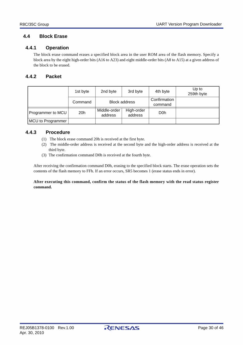
4.4 Block Erase
4.4.1 OperationThe block erase command erases a specified block area in the user ROM area of the flash memory. Specify ablock area by the eight high-order bits (A16 to A23) and eight middle-order bits (A8 to A15) at a given address ofthe block to be erased.
4.4.2 Packet
4.4.3 Procedure(1) The block erase command 20h is received at the first byte.(2) The middle-order address is received at the second byte and the high-order address is received at the
third byte.(3) The confirmation command D0h is received at the fourth byte.
After receiving the confirmation command D0h, erasing to the specified block starts. The erase operation sets thecontents of the flash memory to FFh. If an error occurs, SR5 becomes 1 (erase status ends in error).
After executing this command, confirm the status of the flash memory with the read status registercommand.
1st byte 2nd byte 3rd byte 4th byte Up to 259th byte
Command Block address Confirmation command
Programmer to MCU 20h Middle-orderaddress
High-orderaddress D0h
MCU to Programmer
R8C/35C Group UART Version Program Downloader
REJ05B1378-0100 Rev.1.00 Page 31 of 46Apr. 30, 2010
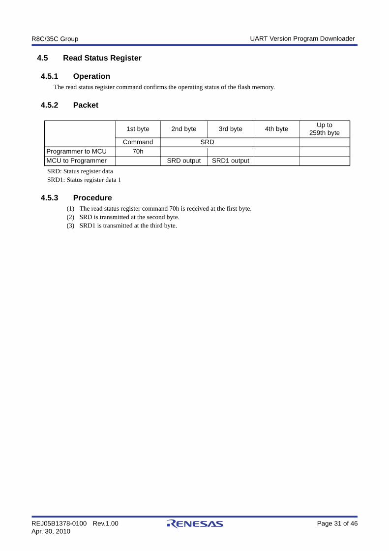
4.5 Read Status Register
4.5.1 OperationThe read status register command confirms the operating status of the flash memory.
4.5.2 Packet
SRD: Status register dataSRD1: Status register data 1
4.5.3 Procedure(1) The read status register command 70h is received at the first byte.(2) SRD is transmitted at the second byte.(3) SRD1 is transmitted at the third byte.
1st byte 2nd byte 3rd byte 4th byte Up to 259th byte
Command SRDProgrammer to MCU 70hMCU to Programmer SRD output SRD1 output
R8C/35C Group UART Version Program Downloader
REJ05B1378-0100 Rev.1.00 Page 32 of 46Apr. 30, 2010
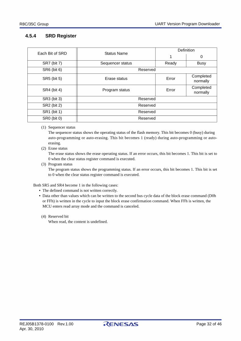
4.5.4 SRD Register
(1) Sequencer statusThe sequencer status shows the operating status of the flash memory. This bit becomes 0 (busy) during auto-programming or auto-erasing. This bit becomes 1 (ready) during auto-programming or auto-erasing.
(2) Erase statusThe erase status shows the erase operating status. If an error occurs, this bit becomes 1. This bit is set to0 when the clear status register command is executed.
(3) Program statusThe program status shows the programming status. If an error occurs, this bit becomes 1. This bit is setto 0 when the clear status register command is executed.
Both SR5 and SR4 become 1 in the following cases:• The defined command is not written correctly.• Data other than values which can be written to the second bus cycle data of the block erase command (D0h
or FFh) is written in the cycle to input the block erase confirmation command. When FFh is written, the MCU enters read array mode and the command is canceled.
(4) Reserved bitWhen read, the content is undefined.
Each Bit of SRD Status NameDefinition
1 0SR7 (bit 7) Sequencer status Ready BusySR6 (bit 6) Reserved
SR5 (bit 5) Erase status Error Completed normally
SR4 (bit 4) Program status Error Completed normally
SR3 (bit 3) ReservedSR2 (bit 2) ReservedSR1 (bit 1) ReservedSR0 (bit 0) Reserved
R8C/35C Group UART Version Program Downloader
REJ05B1378-0100 Rev.1.00 Page 33 of 46Apr. 30, 2010
4.5.5 SRD1 Register
(1) ID checkThese bits indicate the ID check results.
(2) Reserved bitWhen read, the content is undefined.
Each Bit of SRD1 Status NameDefinition
1 0SR15 (bit 7) ReservedSR14 (bit 6) ReservedSR13 (bit 5) ReservedSR12 (bit 4) ReservedSR11 (bit 3)
ID check
00: Not checked01: ID Not matched
10: Reserved11: Checked
SR10 (bit 2)
SR9 (bit 1) ReservedSR8 (bit 0) Reserved
R8C/35C Group UART Version Program Downloader
REJ05B1378-0100 Rev.1.00 Page 34 of 46Apr. 30, 2010
4.6 Clear Status Register
4.6.1 OperationThe clear status register command initializes a status register. Initialize the status register before executing theerase or the page program to the flash memory.
4.6.2 Packet
4.6.3 Procedure(1) The clear status register command 50h is received at the first byte.
1st byte 2nd byte 3rd byte 4th byte Up to 259th byte
CommandProgrammer to MCU 50hMCU to Programmer
R8C/35C Group UART Version Program Downloader
REJ05B1378-0100 Rev.1.00 Page 35 of 46Apr. 30, 2010
4.7 ID Check Function
4.7.1 OperationThis function compares the ID received from the programmer and the user ID code stored in the virtual fixedvector address. The ID check results are stored in SR11 to SR10 in the SRD1 register.
4.7.2 Packet
4.7.3 Procedure(1) The ID check function command F5h is received at the first byte.(2) ID1 to ID7 are received from the second byte to the eighth byte, respectively.
After receiving the ID, the ID check starts. However, a user program area blank product returns the wait state forthe control command from the programmer without performing ID check. When ID1 to ID7 all match, SR11 toSR10 become 11b (verified). If any of the IDs do not match, SR11 to SR10 become 01b (verify not matched).
1st Byte 2nd Byte 3rd Byte 4th Byte Up to 8th Byte
Command IDProgrammer to MCU F5h ID1 ID2 ID3 Up to ID7MCU to Programmer
R8C/35C Group UART Version Program Downloader
REJ05B1378-0100 Rev.1.00 Page 36 of 46Apr. 30, 2010
4.8 Version Information Output Function
4.8.1 OperationThis function transmits version information of the program downloader and user program.
4.8.2 Packet
4.8.3 Procedure(1) The version information output function command FBh is received at the first byte.(2) The program downloader version is transmitted at the high-order second byte first and then the low-
order third byte.(3) The user program version is transmitted at the high-order fourth byte first and then low-order fifth byte.
4.8.4 Version DataFor the example shown below, the program download version is transmitted after 01h is set to the high order and00h to the low order of the program downloader version, and 00h is set to the high order and 10h to the low orderof the user version.
1st Byte 2nd Byte 3rd Byte 4th Byte 5th Byte Up to 259th Byte
Command VersionProgrammer to MCU FBhMCU to Programmer Program downloader User
When the program downloader version is Ver.1.00 and the user version is Ver.0.10:
Program downloader version data(in the bt_r835c.a30 file)
.org version_string
.word 0100h ; Program Downloader version (Ver.1.00)
User version data(in the sect30.inc file for 5. User Program Example)
User_Ver .equ 0010h ; User version (Ver.0.10)
R8C/35C Group UART Version Program Downloader
REJ05B1378-0100 Rev.1.00 Page 37 of 46Apr. 30, 2010
5. User Program ExampleThe program downloader rewrites the user programs other than the user program in block 0 according to theprogrammer. An example of the user program is shown below.
5.1 FunctionThe LEDs connected to I/O ports P3_1, P3_3, P3_4, and P3_6 light.
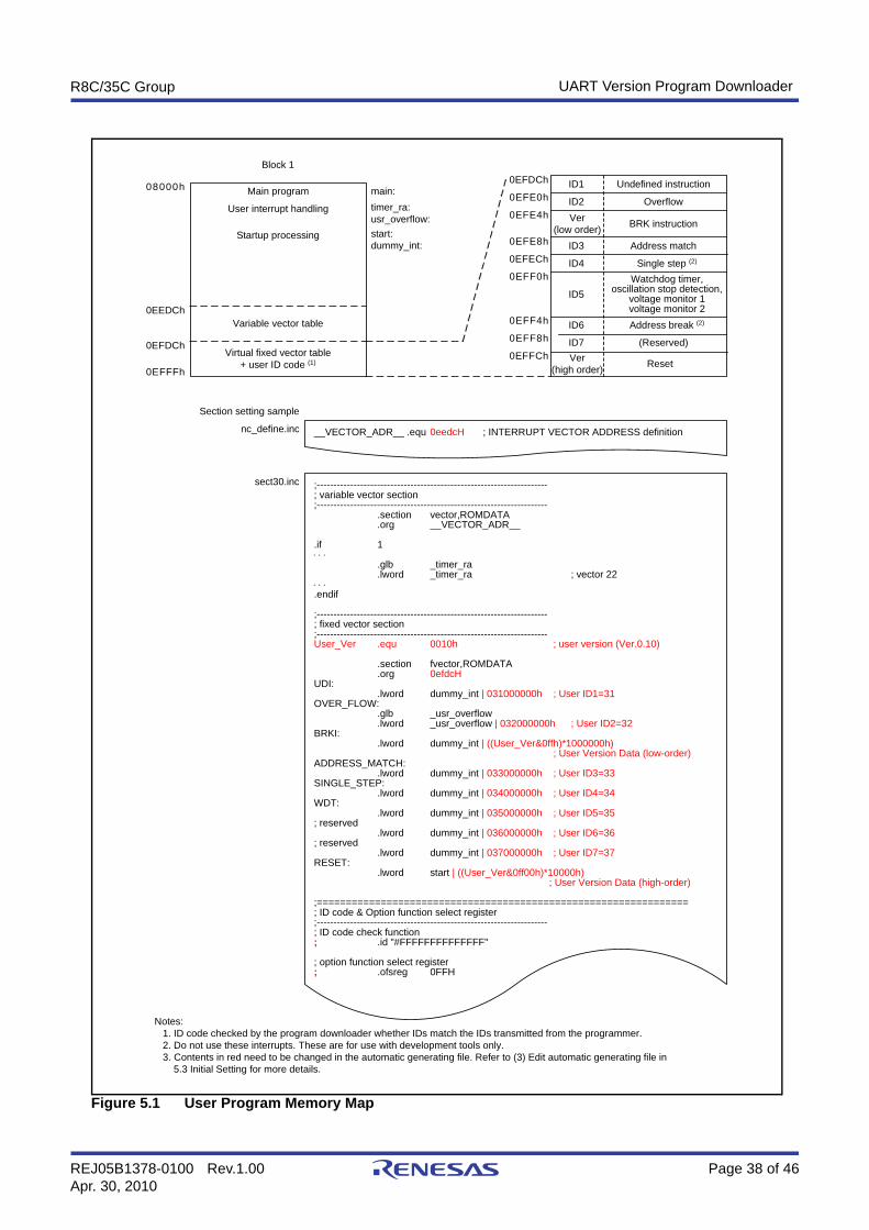
5.2 Memory MapFigure 5.1 shows a User Program Memory Map.
R8C/35C Group UART Version Program Downloader
REJ05B1378-0100 Rev.1.00 Page 38 of 46Apr. 30, 2010
Figure 5.1 User Program Memory Map
Block 1
Virtual fixed vector table+ user ID code (1)
Variable vector table
Notes: 1. ID code checked by the program downloader whether IDs match the IDs transmitted from the programmer. 2. Do not use these interrupts. These are for use with development tools only. 3. Contents in red need to be changed in the automatic generating file. Refer to (3) Edit automatic generating file in 5.3 Initial Setting for more details.
main:
User interrupt handling
Main programtimer_ra:usr_overflow:
__VECTOR_ADR__ .equ 0eedcH ; INTERRUPT VECTOR ADDRESS definitionnc_define.inc
;---------------------------------------------------------------------; variable vector section;---------------------------------------------------------------------
.section vector,ROMDATA
.org __VECTOR_ADR__
.if 1⋅ ⋅ ⋅
.glb _timer_ra
.lword _timer_ra ; vector 22⋅ ⋅ ⋅.endif
;---------------------------------------------------------------------; fixed vector section;---------------------------------------------------------------------User_Ver .equ 0010h ; user version (Ver.0.10)
.section fvector,ROMDATA
.org 0efdcHUDI:
.lword dummy_int | 031000000h ; User ID1=31OVER_FLOW:
.glb _usr_overflow
.lword _usr_overflow | 032000000h ; User ID2=32BRKI:
.lword dummy_int | ((User_Ver&0ffh)*1000000h); User Version Data (low-order)
ADDRESS_MATCH:.lword dummy_int | 033000000h ; User ID3=33
SINGLE_STEP:.lword dummy_int | 034000000h ; User ID4=34
WDT:.lword dummy_int | 035000000h ; User ID5=35
; reserved.lword dummy_int | 036000000h ; User ID6=36
; reserved.lword dummy_int | 037000000h ; User ID7=37
RESET:.lword start | ((User_Ver&0ff00h)*10000h)
; User Version Data (high-order)
;================================================================; ID code & Option function select register;---------------------------------------------------------------------; ID code check function; .id "#FFFFFFFFFFFFFF"
; option function select register; .ofsreg 0FFH
sect30.inc
Section setting sample
0EFDCh
08000h
0EFFFh
0EEDCh
Startup processing start:dummy_int:
Undefined instruction
Overflow
Address match
Single step (2)
Watchdog timer,oscillation stop detection,
voltage monitor 1voltage monitor 2Address break (2)
(Reserved)
Reset
ID1
ID2
ID7
ID4
ID5
ID6
BRK instruction
ID3
0EFDCh
0EFE0h
0EFE8h
0EFECh
0EFF0h
0EFF4h
0EFF8h
0EFFCh
0EFE4h Ver(low order)
Ver(high order)
R8C/35C Group UART Version Program Downloader
REJ05B1378-0100 Rev.1.00 Page 39 of 46Apr. 30, 2010
5.3 Initial Settings(1) Vector table
Allocate the virtual fixed vector table to block 1 to use an interrupt by the user program.(2) ID code
Set an ID code in the virtual fixed vector table. Do not opt to generate an ID code file when compiling.(3) Edit automatic generating file
When the project type is made in the Application and the initial setting file is automatically generated by the High-performance Embedded Workshop (HEW), change the sect30.inc file and nc_define.inc file as follows(see Figure 5.1):
• Change the allocation address of the locatable table to 0EEDCh, and the virtual fixed vector table to 0EFDCh.
• Set an additional ID code to the virtual fixed vector table.• Add the symbol definition of the user version data and user version data setting to the virtual fixed vector
table.• Comment out the assembler expansion function direction instructions “.ID” (set an ID code) and
“.OFSREG” (set a value to the OFS register).
R8C/35C Group UART Version Program Downloader
REJ05B1378-0100 Rev.1.00 Page 40 of 46Apr. 30, 2010
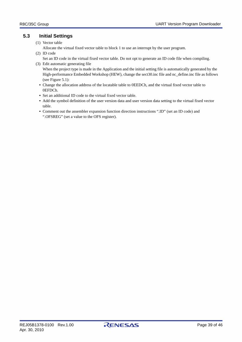
6. Programmer Example
6.1 Control Pins(1) Pins TXD and RXD
These pins are for transmitting and receiving in UART mode.(2) RESET pin
This pin controls an MCU reset from the programmer.(3) Pins VCC and VSS
Adjust high level from the programmer to the MCU’s VCC level and low level from the programmer to the MCU’s VSS level, respectively.
Figure 6.1 Programmer Configuration
R8C/35C Group
MODE
User reset signal
TXD
RXDRXD input
RESETReset input
TXD output
R8C/35C Group UART Version Program Downloader
REJ05B1378-0100 Rev.1.00 Page 41 of 46Apr. 30, 2010
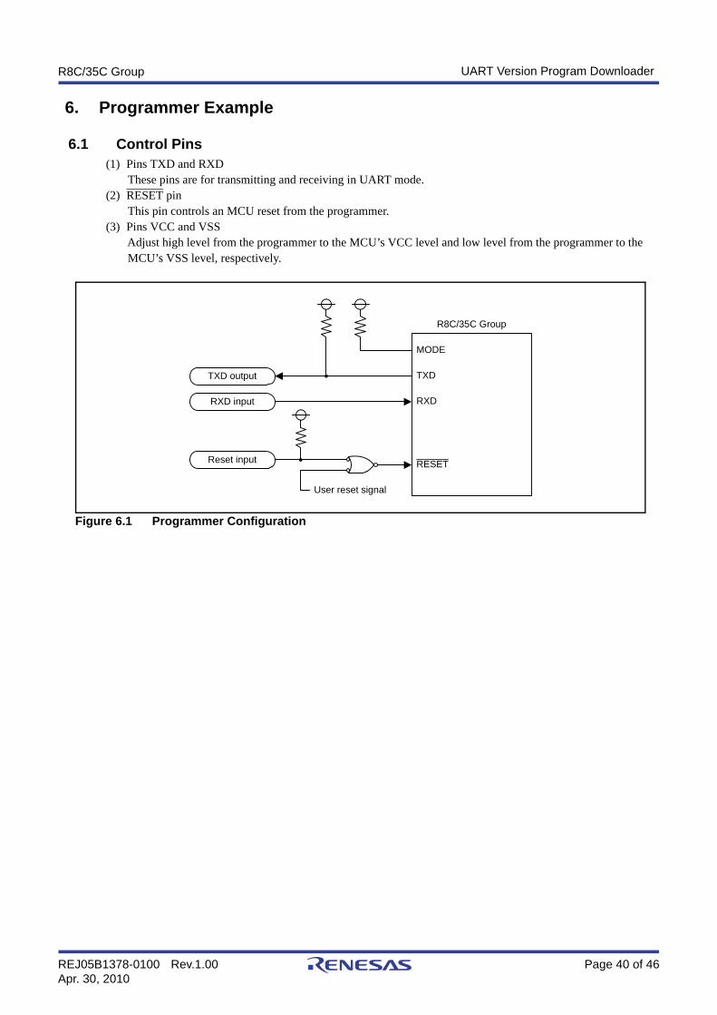
6.2 Programmer FunctionsThe following are the functions necessary for the programmer:
• Blank Check• Erase• Program• Verify• Read
6.3 Blank CheckData (program) in the specified area automatically or manually is read from the MCU’s on-chip flash memory. Theprogrammer confirms that all read data is blank (FFh).
Programmer MCU
Bits SR11 and SR10 in SRD1• 00b (not verified), 01b (verification not matched) → Go to ID check• 11b (verified) → Go to blank check without ID check
Bits SR11 and SR10 in SRD1• 01b (verification not matched) → Process stopped by ID check error• 11b (verified) → Go to next step
When received data is• All FFh→ Go to next step• Other than above→ Process stopped by blank check error
• When the blank check for the specified area is not completed → Return to page read process• When blank check is completed → Blank check OK
Start ID Check
ID Check OK
Start Blank Check
Blank check OK
Transmit read status register command 70h
Receive SRD and SRD1
Transmit ID check commands F5h and ID1 to ID7
Receive SRD and SRD1
Transmit read status register command 70h
Receive data (256 bytes)
Transmit page read command FFh, middle-order address,and high-order address
R8C/35C Group UART Version Program Downloader
REJ05B1378-0100 Rev.1.00 Page 42 of 46Apr. 30, 2010
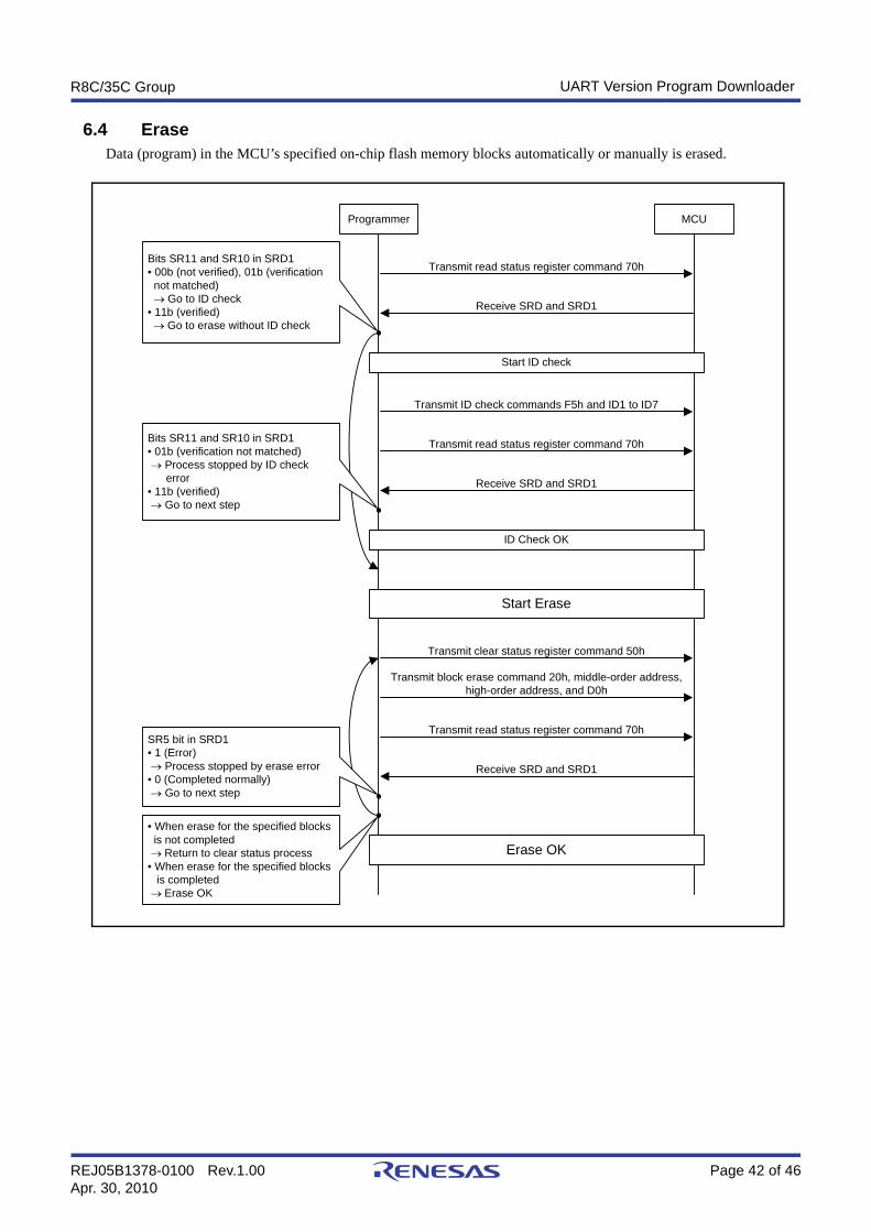
6.4 EraseData (program) in the MCU’s specified on-chip flash memory blocks automatically or manually is erased.
Programmer MCU
Bits SR11 and SR10 in SRD1• 00b (not verified), 01b (verification not matched) → Go to ID check• 11b (verified) → Go to erase without ID check
Bits SR11 and SR10 in SRD1• 01b (verification not matched) → Process stopped by ID check error• 11b (verified) → Go to next step
SR5 bit in SRD1• 1 (Error) → Process stopped by erase error• 0 (Completed normally) → Go to next step
• When erase for the specified blocks is not completed → Return to clear status process• When erase for the specified blocks is completed → Erase OK
Transmit read status register command 70h
Receive SRD and SRD1
Start ID check
Transmit ID check commands F5h and ID1 to ID7
Receive SRD and SRD1
Transmit read status register command 70h
ID Check OK
Start Erase
Transmit clear status register command 50h
Erase OK
Transmit block erase command 20h, middle-order address,high-order address, and D0h
Transmit read status register command 70h
Receive SRD and SRD1
R8C/35C Group UART Version Program Downloader
REJ05B1378-0100 Rev.1.00 Page 43 of 46Apr. 30, 2010
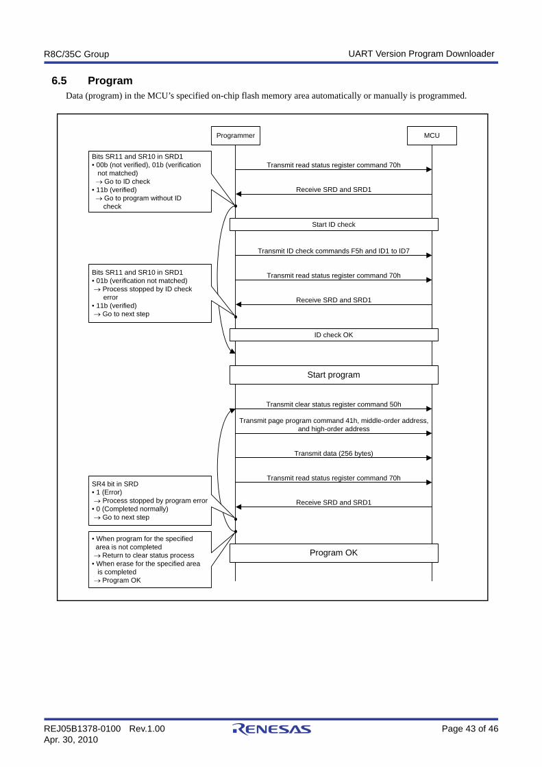
6.5 ProgramData (program) in the MCU’s specified on-chip flash memory area automatically or manually is programmed.
Programmer MCU
Bits SR11 and SR10 in SRD1• 00b (not verified), 01b (verification not matched) → Go to ID check• 11b (verified) → Go to program without ID check
Bits SR11 and SR10 in SRD1• 01b (verification not matched) → Process stopped by ID check error• 11b (verified) → Go to next step
SR4 bit in SRD• 1 (Error) → Process stopped by program error• 0 (Completed normally) → Go to next step
• When program for the specified area is not completed → Return to clear status process• When erase for the specified area is completed → Program OK
Program OK
Transmit clear status register command 50h
Transmit page program command 41h, middle-order address,and high-order address
Transmit read status register command 70h
Receive SRD and SRD1
Transmit data (256 bytes)
Start ID check
ID check OK
Start program
Transmit read status register command 70h
Receive SRD and SRD1
Transmit ID check commands F5h and ID1 to ID7
Receive SRD and SRD1
Transmit read status register command 70h
R8C/35C Group UART Version Program Downloader
REJ05B1378-0100 Rev.1.00 Page 44 of 46Apr. 30, 2010
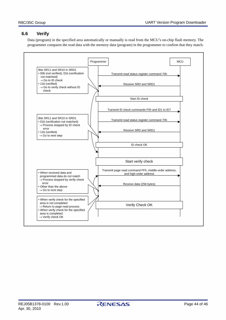
6.6 VerifyData (program) in the specified area automatically or manually is read from the MCU’s on-chip flash memory. Theprogrammer compares the read data with the memory data (program) in the programmer to confirm that they match.
Programmer MCU
Bits SR11 and SR10 in SRD1• 00b (not verified), 01b (verification not matched) → Go to ID check• 11b (verified) → Go to verify check without ID check
Bits SR11 and SR10 in SRD1• 01b (verification not matched) → Process stopped by ID check error• 11b (verified) → Go to next step
• When received data and programmed data do not match → Process stopped by verify check error• Other than the above → Go to next step
• When verify check for the specified area is not completed → Return to page read process• When verify check for the specified area is completed → Verify check OK
Start ID check
ID check OK
Start verify check
Verify Check OK
Transmit read status register command 70h
Receive SRD and SRD1
Transmit ID check commands F5h and ID1 to ID7
Receive SRD and SRD1
Transmit read status register command 70h
Receive data (256 bytes)
Transmit page read command FFh, middle-order address,and high-order address
R8C/35C Group UART Version Program Downloader
REJ05B1378-0100 Rev.1.00 Page 45 of 46Apr. 30, 2010
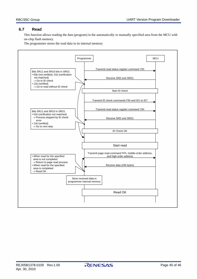
6.7 ReadThis function allows reading the data (program) in the automatically or manually specified area from the MCU withon-chip flash memory.The programmer stores the read data in its internal memory
Programmer MCU
Bits SR11 and SR10 bits in SRD1• 00b (not verified), 01b (verification not matched) → Go to ID check• 11b (verified) → Go to read without ID check
Bits SR11 and SR10 in SRD1• 01b (verification not matched) → Process stopped by ID check error• 11b (verified) → Go to next step
• When read for the specified area is not completed → Return to page read process• When read for the specified area is completed → Read OK
Store received data inprogrammer internal memory
Start ID check
ID Check OK
Start read
Read OK
Transmit read status register command 70h
Receive SRD and SRD1
Transmit ID check commands F5h and ID1 to ID7
Receive SRD and SRD1
Transmit read status register command 70h
Receive data (256 bytes)
Transmit page read command FFh, middle-order address,and high-order address
R8C/35C Group UART Version Program Downloader
REJ05B1378-0100 Rev.1.00 Page 46 of 46Apr. 30, 2010
7. Sample Programming CodeA sample program can be downloaded from the Renesas Electronics website.To download, click “Application Notes” in the left-hand side menu of the R8C Family page.
8. Reference DocumentsR8C/35C Group User’s Manual: HardwareRev.1.00The latest version can be downloaded from the Renesas Electronics website.
Technical Update/Technical NewsThe latest information can be downloaded from the Renesas Electronics website.
Website and SupportRenesas Electronics websitehttp://www.renesas.com/
Inquirieshttp://www.renesas.com/inquiry
A - 1
Revision History R8C/35C Group UART Version Program Downloader
Rev. DateDescription
Page Summary1.00 Apr 30, 2010 — First edition issued
All trademarks and registered trademarks are the property of their respective owners.
General Precautions in the Handling of MPU/MCU Products
The following usage notes are applicable to all MPU/MCU products from Renesas. For detailed usage notes on the products covered by this manual, refer to the relevant sections of the manual. If the descriptions under General Precautions in the Handling of MPU/MCU Products and in the body of the manual differ from each other, the description in the body of the manual takes precedence.
1. Handling of Unused Pins Handle unused pins in accord with the directions given under Handling of Unused Pins in the manual. The input pins of CMOS products are generally in the high-impedance state. In operation
with an unused pin in the open-circuit state, extra electromagnetic noise is induced in the vicinity of LSI, an associated shoot-through current flows internally, and malfunctions occur due to the false recognition of the pin state as an input signal become possible. Unused pins should be handled as described under Handling of Unused Pins in the manual.
2. Processing at Power-on The state of the product is undefined at the moment when power is supplied. The states of internal circuits in the LSI are indeterminate and the states of register
settings and pins are undefined at the moment when power is supplied. In a finished product where the reset signal is applied to the external reset pin, the states of pins are not guaranteed from the moment when power is supplied until the reset process is completed. In a similar way, the states of pins in a product that is reset by an on-chip power-on reset function are not guaranteed from the moment when power is supplied until the power reaches the level at which resetting has been specified.
3. Prohibition of Access to Reserved Addresses Access to reserved addresses is prohibited. The reserved addresses are provided for the possible future expansion of functions. Do
not access these addresses; the correct operation of LSI is not guaranteed if they are accessed.
4. Clock Signals After applying a reset, only release the reset line after the operating clock signal has become stable. When switching the clock signal during program execution, wait until the target clock signal has stabilized. When the clock signal is generated with an external resonator (or from an external
oscillator) during a reset, ensure that the reset line is only released after full stabilization of the clock signal. Moreover, when switching to a clock signal produced with an external resonator (or by an external oscillator) while program execution is in progress, wait until the target clock signal is stable.
5. Differences between Products Before changing from one product to another, i.e. to one with a different part number, confirm that the change will not lead to problems. The characteristics of MPU/MCU in the same group but having different part numbers may
differ because of the differences in internal memory capacity and layout pattern. When changing to products of different part numbers, implement a system-evaluation test for each of the products.
Notice1. All information included in this document is current as of the date this document is issued. Such information, however, is subject to change without any prior notice. Before purchasing or using any Renesas
Electronics products listed herein, please confirm the latest product information with a Renesas Electronics sales office. Also, please pay regular and careful attention to additional and different information to
be disclosed by Renesas Electronics such as that disclosed through our website.
2. Renesas Electronics does not assume any liability for infringement of patents, copyrights, or other intellectual property rights of third parties by or arising from the use of Renesas Electronics products or
technical information described in this document. No license, express, implied or otherwise, is granted hereby under any patents, copyrights or other intellectual property rights of Renesas Electronics or
others.
3. You should not alter, modify, copy, or otherwise misappropriate any Renesas Electronics product, whether in whole or in part.
4. Descriptions of circuits, software and other related information in this document are provided only to illustrate the operation of semiconductor products and application examples. You are fully responsible for
the incorporation of these circuits, software, and information in the design of your equipment. Renesas Electronics assumes no responsibility for any losses incurred by you or third parties arising from the
use of these circuits, software, or information.
5. When exporting the products or technology described in this document, you should comply with the applicable export control laws and regulations and follow the procedures required by such laws and
regulations. You should not use Renesas Electronics products or the technology described in this document for any purpose relating to military applications or use by the military, including but not limited to
the development of weapons of mass destruction. Renesas Electronics products and technology may not be used for or incorporated into any products or systems whose manufacture, use, or sale is
prohibited under any applicable domestic or foreign laws or regulations.
6. Renesas Electronics has used reasonable care in preparing the information included in this document, but Renesas Electronics does not warrant that such information is error free. Renesas Electronics
assumes no liability whatsoever for any damages incurred by you resulting from errors in or omissions from the information included herein.
7. Renesas Electronics products are classified according to the following three quality grades: "Standard", "High Quality", and "Specific". The recommended applications for each Renesas Electronics product
depends on the product's quality grade, as indicated below. You must check the quality grade of each Renesas Electronics product before using it in a particular application. You may not use any Renesas
Electronics product for any application categorized as "Specific" without the prior written consent of Renesas Electronics. Further, you may not use any Renesas Electronics product for any application for
which it is not intended without the prior written consent of Renesas Electronics. Renesas Electronics shall not be in any way liable for any damages or losses incurred by you or third parties arising from the
use of any Renesas Electronics product for an application categorized as "Specific" or for which the product is not intended where you have failed to obtain the prior written consent of Renesas Electronics.
The quality grade of each Renesas Electronics product is "Standard" unless otherwise expressly specified in a Renesas Electronics data sheets or data books, etc.
"Standard": Computers; office equipment; communications equipment; test and measurement equipment; audio and visual equipment; home electronic appliances; machine tools;
personal electronic equipment; and industrial robots.
"High Quality": Transportation equipment (automobiles, trains, ships, etc.); traffic control systems; anti-disaster systems; anti-crime systems; safety equipment; and medical equipment not specifically
designed for life support.
"Specific": Aircraft; aerospace equipment; submersible repeaters; nuclear reactor control systems; medical equipment or systems for life support (e.g. artificial life support devices or systems), surgical
implantations, or healthcare intervention (e.g. excision, etc.), and any other applications or purposes that pose a direct threat to human life.
8. You should use the Renesas Electronics products described in this document within the range specified by Renesas Electronics, especially with respect to the maximum rating, operating supply voltage
range, movement power voltage range, heat radiation characteristics, installation and other product characteristics. Renesas Electronics shall have no liability for malfunctions or damages arising out of the
use of Renesas Electronics products beyond such specified ranges.
9. Although Renesas Electronics endeavors to improve the quality and reliability of its products, semiconductor products have specific characteristics such as the occurrence of failure at a certain rate and
malfunctions under certain use conditions. Further, Renesas Electronics products are not subject to radiation resistance design. Please be sure to implement safety measures to guard them against the
possibility of physical injury, and injury or damage caused by fire in the event of the failure of a Renesas Electronics product, such as safety design for hardware and software including but not limited to
redundancy, fire control and malfunction prevention, appropriate treatment for aging degradation or any other appropriate measures. Because the evaluation of microcomputer software alone is very difficult,
please evaluate the safety of the final products or system manufactured by you.
10. Please contact a Renesas Electronics sales office for details as to environmental matters such as the environmental compatibility of each Renesas Electronics product. Please use Renesas Electronics
products in compliance with all applicable laws and regulations that regulate the inclusion or use of controlled substances, including without limitation, the EU RoHS Directive. Renesas Electronics assumes
no liability for damages or losses occurring as a result of your noncompliance with applicable laws and regulations.
11. This document may not be reproduced or duplicated, in any form, in whole or in part, without prior written consent of Renesas Electronics.
12. Please contact a Renesas Electronics sales office if you have any questions regarding the information contained in this document or Renesas Electronics products, or if you have any other inquiries.
(Note 1) "Renesas Electronics" as used in this document means Renesas Electronics Corporation and also includes its majority-owned subsidiaries.
(Note 2) "Renesas Electronics product(s)" means any product developed or manufactured by or for Renesas Electronics.
http://www.renesas.comRefer to "http://www.renesas.com/" for the latest and detailed information.
Renesas Electronics America Inc. 2880 Scott Boulevard Santa Clara, CA 95050-2554, U.S.A.Tel: +1-408-588-6000, Fax: +1-408-588-6130Renesas Electronics Canada Limited1101 Nicholson Road, Newmarket, Ontario L3Y 9C3, CanadaTel: +1-905-898-5441, Fax: +1-905-898-3220Renesas Electronics Europe LimitedDukes Meadow, Millboard Road, Bourne End, Buckinghamshire, SL8 5FH, U.KTel: +44-1628-585-100, Fax: +44-1628-585-900Renesas Electronics Europe GmbHArcadiastrasse 10, 40472 Düsseldorf, Germany Tel: +49-211-65030, Fax: +49-211-6503-1327 Renesas Electronics (China) Co., Ltd.7th Floor, Quantum Plaza, No.27 ZhiChunLu Haidian District, Beijing 100083, P.R.China Tel: +86-10-8235-1155, Fax: +86-10-8235-7679Renesas Electronics (Shanghai) Co., Ltd.Unit 204, 205, AZIA Center, No.1233 Lujiazui Ring Rd., Pudong District, Shanghai 200120, China Tel: +86-21-5877-1818, Fax: +86-21-6887-7858 / -7898 Renesas Electronics Hong Kong LimitedUnit 1601-1613, 16/F., Tower 2, Grand Century Place, 193 Prince Edward Road West, Mongkok, Kowloon, Hong KongTel: +852-2886-9318, Fax: +852 2886-9022/9044Renesas Electronics Taiwan Co., Ltd.7F, No. 363 Fu Shing North Road Taipei, TaiwanTel: +886-2-8175-9600, Fax: +886 2-8175-9670Renesas Electronics Singapore Pte. Ltd. 1 harbourFront Avenue, #06-10, keppel Bay Tower, Singapore 098632Tel: +65-6213-0200, Fax: +65-6278-8001Renesas Electronics Malaysia Sdn.Bhd. Unit 906, Block B, Menara Amcorp, Amcorp Trade Centre, No. 18, Jln Persiaran Barat, 46050 Petaling Jaya, Selangor Darul Ehsan, MalaysiaTel: +60-3-7955-9390, Fax: +60-3-7955-9510Renesas Electronics Korea Co., Ltd.11F., Samik Lavied' or Bldg., 720-2 Yeoksam-Dong, Kangnam-Ku, Seoul 135-080, KoreaTel: +82-2-558-3737, Fax: +82-2-558-5141
SALES OFFICES
© 2010 Renesas Electronics Corporation. All rights reserved.
Colophon 1.0


![[PPT]UART and UART Driver - University at Buffalobina/cse321/fall2009/UARTDriver.ppt · Web viewUART and UART Driver B. Ramamurthy * UART UART: Universal Asynchronous Receiver/Transmitter](https://img.pdfslide.net/doc/110x75/5b2ab3637f8b9a55068b752f/pptuart-and-uart-driver-university-at-binacse321fall2009uartdriverppt.jpg)