Embed Size (px)
Citation preview
UC15 Hardware Design
UMTS/HSDPA Module Series
Rev. UC15_Hardware_Design_V1.6
Date: 2015-02-04
www.quectel.com
UMTS/HSDPA Module Series UC15 Hardware Design
UC15_Hardware_Design Confidential / Released 1 / 79
Our aim is to provide customers with timely and comprehensive service. For any
assistance, please contact our company headquarters:
Quectel Wireless Solutions Co., Ltd.
Office 501, Building 13, No.99, Tianzhou Road, Shanghai, China, 200233
Tel: +86 21 5108 6236
Mail: [email protected]
Or our local office, for more information, please visit:
http://www.quectel.com/support/salesupport.aspx
For technical support, to report documentation errors, please visit:
http://www.quectel.com/support/techsupport.aspx
Or Email: [email protected]
GENERAL NOTES
QUECTEL OFFERS THIS INFORMATION AS A SERVICE TO ITS CUSTOMERS. THE INFORMATION
PROVIDED IS BASED UPON CUSTOMERS’ REQUIREMENTS. QUECTEL MAKES EVERY EFFORT
TO ENSURE THE QUALITY OF THE INFORMATION IT MAKES AVAILABLE. QUECTEL DOES NOT
MAKE ANY WARRANTY AS TO THE INFORMATION CONTAINED HEREIN, AND DOES NOT ACCEPT
ANY LIABILITY FOR ANY INJURY, LOSS OR DAMAGE OF ANY KIND INCURRED BY USE OF OR
RELIANCE UPON THE INFORMATION. THE INFORMATION SUPPLIED HEREIN IS SUBJECT TO
CHANGE WITHOUT PRIOR NOTICE.
COPYRIGHT
THIS INFORMATION CONTAINED HERE IS PROPRIETARY TECHNICAL INFORMATION OF
QUECTEL CO., LTD. TRANSMITTABLE, REPRODUCTION, DISSEMINATION AND EDITING OF THIS
DOCUMENT AS WELL AS UTILIZATION OF THIS CONTENTS ARE FORBIDDEN WITHOUT
PERMISSION. OFFENDERS WILL BE HELD LIABLE FOR PAYMENT OF DAMAGES. ALL RIGHTS
ARE RESERVED IN THE EVENT OF A PATENT GRANT OR REGISTRATION OF A UTILITY MODEL
OR DESIGN.
Copyright © Quectel Wireless Solutions Co., Ltd. 2015. All rights reserved.
Quectel
Confidential
UMTS/HSDPA Module Series UC15 Hardware Design
UC15_Hardware_Design Confidential / Released 2 / 79
About the Document
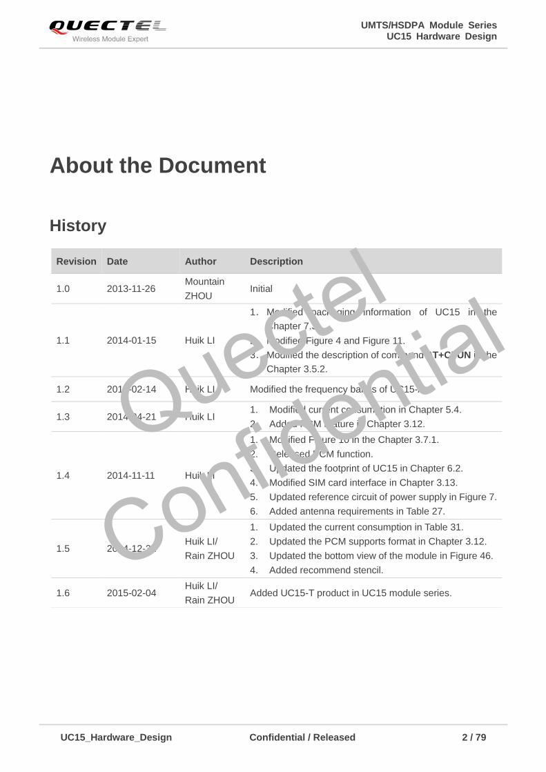
History
Revision Date Author Description
1.0 2013-11-26 Mountain
ZHOU Initial
1.1 2014-01-15 Huik LI
1. Modified packaging information of UC15 in the
Chapter 7.3.
2. Modified Figure 4 and Figure 11.
3. Modified the description of command AT+CFUN in the
Chapter 3.5.2.
1.2 2014-02-14 Huik LI Modified the frequency bands of UC15-A.
1.3 2014-04-21 Huik LI 1. Modified current consumption in Chapter 5.4.
2. Added PCM feature in Chapter 3.12.
1.4 2014-11-11 Huik LI
1. Modified Figure 10 in the Chapter 3.7.1.
2. Released PCM function.
3. Updated the footprint of UC15 in Chapter 6.2.
4. Modified SIM card interface in Chapter 3.13.
5. Updated reference circuit of power supply in Figure 7.
6. Added antenna requirements in Table 27.
1.5 2014-12-31 Huik LI/
Rain ZHOU
1. Updated the current consumption in Table 31.
2. Updated the PCM supports format in Chapter 3.12.
3. Updated the bottom view of the module in Figure 46.
4. Added recommend stencil.
1.6 2015-02-04 Huik LI/
Rain ZHOU Added UC15-T product in UC15 module series.
Quectel
Confidential
UMTS/HSDPA Module Series UC15 Hardware Design
UC15_Hardware_Design Confidential / Released 3 / 79
Contents
About the Document ................................................................................................................................... 2
Contents ....................................................................................................................................................... 3
Table Index ................................................................................................................................................... 5
Figure Index ................................................................................................................................................. 6
1 Introduction .......................................................................................................................................... 8
1.1. Safety Information...................................................................................................................... 9
2 Product Concept ................................................................................................................................ 10
2.1. General Description ................................................................................................................. 10
2.2. Key Features ........................................................................................................................... 11
2.3. Functional Diagram ................................................................................................................. 13
2.4. Evaluation Board ..................................................................................................................... 14
3 Application Interface ......................................................................................................................... 15
3.1. General Description ................................................................................................................. 15
3.2. Pin Assignment ........................................................................................................................ 16
3.3. Pin Description ......................................................................................................................... 17
3.4. Operating Modes ..................................................................................................................... 22
3.5. Power Saving ........................................................................................................................... 23
3.5.1. Sleep Mode .................................................................................................................... 23
3.5.1.1. UART Application ................................................................................................. 23
3.5.1.2. USB Application with Suspend Function ............................................................. 24
3.5.1.3. USB Application without Suspend Function ........................................................ 25
3.5.2. Minimum Functionality Mode ......................................................................................... 26
3.6. Power Supply ........................................................................................................................... 26
3.6.1. Power Supply Pins ......................................................................................................... 26
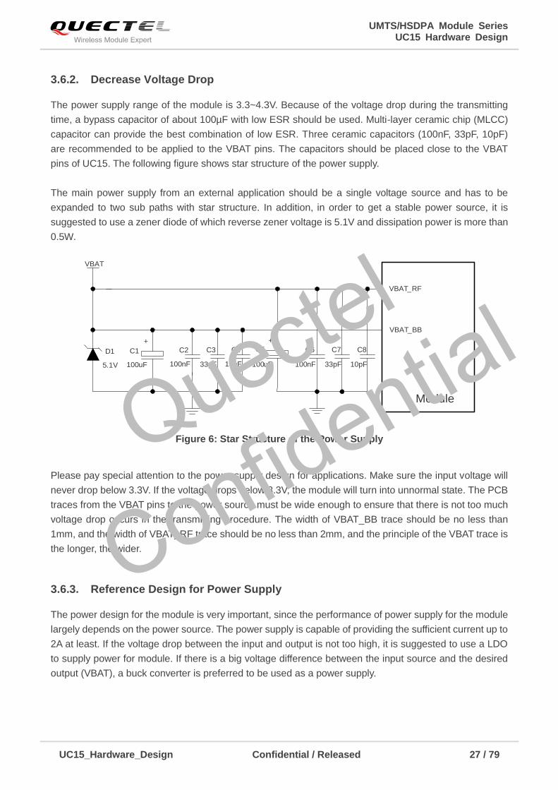
3.6.2. Decrease Voltage Drop .................................................................................................. 27
3.6.3. Reference Design for Power Supply .............................................................................. 27
3.6.4. Monitor the Power Supply .............................................................................................. 28
3.6.5. VDD_EXT ....................................................................................................................... 28
3.7. Turn on and off Scenarios ....................................................................................................... 29
3.7.1. Turn on Module by PWRKEY Pin .................................................................................. 29
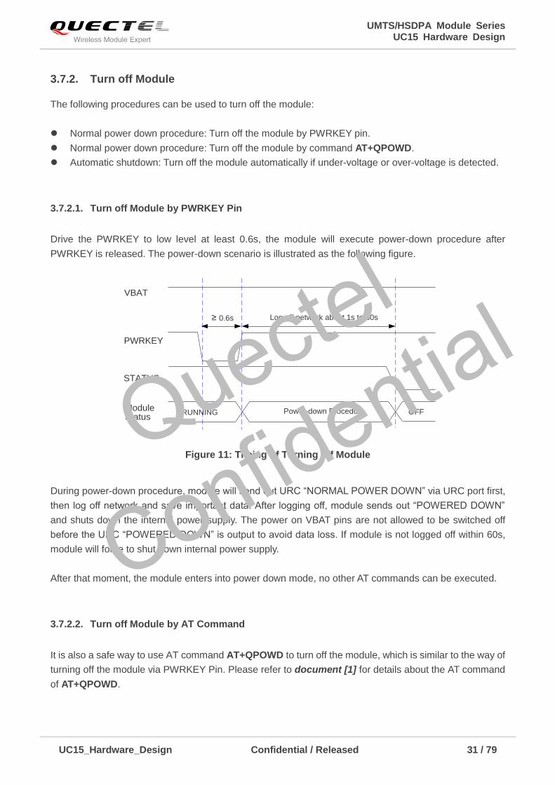
3.7.2. Turn off Module .............................................................................................................. 31
3.7.2.1. Turn off Module by PWRKEY Pin ........................................................................ 31
3.7.2.2. Turn off Module by AT Command ........................................................................ 31
3.7.2.3. Automatic Shutdown ............................................................................................ 32
3.8. Reset the Module..................................................................................................................... 32
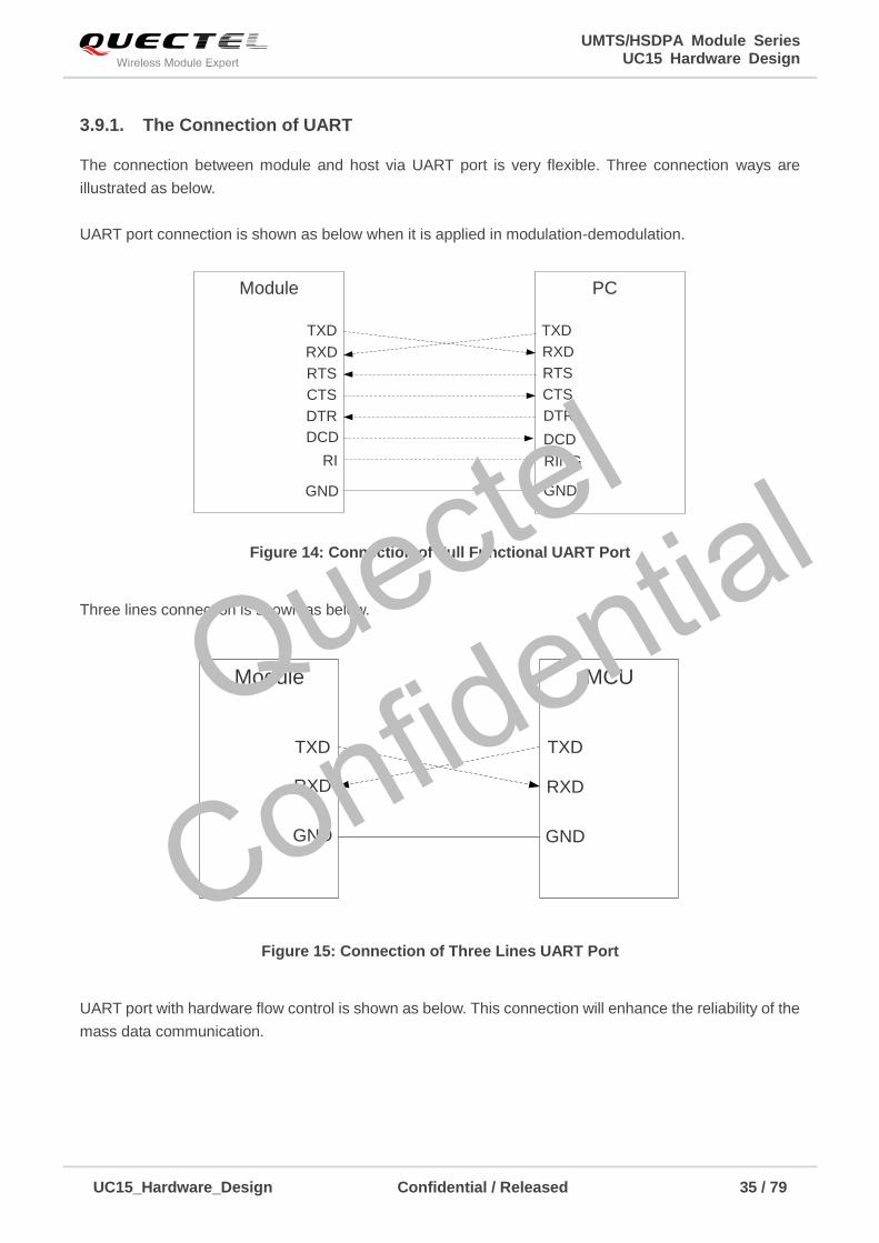
3.9. UART Interface ........................................................................................................................ 34
3.9.1. The Connection of UART ............................................................................................... 35
3.9.2. UART Application ........................................................................................................... 36
3.10. Behavior of the RI .................................................................................................................... 38
3.11. Analog Audio Interface ............................................................................................................ 39
Quectel
Confidential
UMTS/HSDPA Module Series UC15 Hardware Design
UC15_Hardware_Design Confidential / Released 4 / 79
3.11.1. Decrease TDD Noise and Other Noise .......................................................................... 40
3.11.2. Microphone Interfaces Application ................................................................................. 41
3.11.3. Receiver and Speaker Interface Application .................................................................. 42
3.11.4. Earphone Interface Application ...................................................................................... 44
3.12. PCM and I2C Interface ............................................................................................................ 45
3.13. USIM Card Interface ................................................................................................................ 47
3.14. USB Interface .......................................................................................................................... 50
3.15. ADC Function .......................................................................................................................... 51
3.16. Network Status Indication ........................................................................................................ 52
3.17. Operating Status Indication ..................................................................................................... 53
4 Antenna Interface ............................................................................................................................... 55
4.1. Antenna Interface .................................................................................................................... 55
4.1.1. Pin Definition .................................................................................................................. 55
4.1.2. Operating Frequency ..................................................................................................... 55
4.1.3. Reference Design .......................................................................................................... 56
4.2. Antenna Installation ................................................................................................................. 56
4.2.1. Antenna Requirement .................................................................................................... 56
4.2.2. Install the Antenna with RF Connector .......................................................................... 57
5 Electrical, Reliability and Radio Characteristics ............................................................................ 60
5.1. Absolute Maximum Ratings ..................................................................................................... 60
5.2. Power Supply Ratings ............................................................................................................. 61
5.3. Operating Temperature ............................................................................................................ 61
5.4. Current Consumption .............................................................................................................. 62
5.5. RF Output Power ..................................................................................................................... 64
5.6. RF Receiving Sensitivity .......................................................................................................... 64
5.7. Electrostatic Discharge ............................................................................................................ 65
6 Mechanical Dimensions .................................................................................................................... 66
6.1. Mechanical Dimensions of the Module.................................................................................... 66
6.2. Footprint of Recommendation ................................................................................................. 68
6.3. Top View of the Module ........................................................................................................... 70
6.4. Bottom View of the Module ...................................................................................................... 70
7 Storage and Manufacturing .............................................................................................................. 71
7.1. Storage..................................................................................................................................... 71
7.2. Manufacturing and Welding ..................................................................................................... 71
7.3. Packaging ................................................................................................................................ 73
8 Appendix A Reference ....................................................................................................................... 74
9 Appendix B GPRS Coding Scheme ................................................................................................. 77
10 Appendix C GPRS Multi-slot Class .................................................................................................. 78
11 Appendix D EDGE Modulation and Coding Scheme ..................................................................... 79
Quectel
Confidential
UMTS/HSDPA Module Series UC15 Hardware Design
UC15_Hardware_Design Confidential / Released 5 / 79
Table Index
TABLE 1: FREQUENCY BANDS OF UC15 SERIES ........................................................................................ 10
TABLE 2: UC15 KEY FEATURES ...................................................................................................................... 11
TABLE 3: IO PARAMETERS DEFINITION ........................................................................................................ 17
TABLE 4: PIN DESCRIPTION ........................................................................................................................... 17
TABLE 5: OVERVIEW OF OPERATING MODES ............................................................................................. 22
TABLE 6: VBAT AND GND PIN ......................................................................................................................... 26
TABLE 7: ELECTRICAL CHARACTERISTICS OF VDD_EXT ......................................................................... 28
TABLE 8: PWRKEY PIN DESCRIPTION .......................................................................................................... 29
TABLE 9: RESET_N PIN DESCRIPTION ......................................................................................................... 32
TABLE 10: PIN DEFINITION OF THE UART INTERFACE ............................................................................... 34
TABLE 11: LOGIC LEVELS OF DIGITAL I/O .................................................................................................... 34
TABLE 12: BEHAVIOR OF THE RI ................................................................................................................... 39
TABLE 13: PIN DEFINITION OF THE AUDIO INTERFACE ............................................................................. 39
TABLE 14: MICROPHONE CHARACTERISTICS............................................................................................. 44
TABLE 15: SPEAKER CHARACTERISTICS .................................................................................................... 44
TABLE 16: PIN DEFINITION OF PCM AND I2C INTERFACE .......................................................................... 46
TABLE 17: PIN DEFINITION OF THE USIM INTERFACES ............................................................................. 47
TABLE 18: USB PIN DESCRIPTION ................................................................................................................ 50
TABLE 19: PIN DEFINITION OF THE ADC ...................................................................................................... 52
TABLE 20: CHARACTERISTICS OF THE ADC ................................................................................................ 52
TABLE 21: PIN DEFINITION OF NETWORK INDICATOR ............................................................................... 52
TABLE 22: WORKING STATE OF THE NETWORK INDICATOR..................................................................... 52
TABLE 23: PIN DEFINITION OF STATUS ........................................................................................................ 53
TABLE 24: PIN DEFINITION OF THE RF ANTENNA ....................................................................................... 55
TABLE 25: MODULE OPERATING FREQUENCIES ........................................................................................ 55
TABLE 26: ANTENNA CABLE REQUIREMENTS ............................................................................................. 56
TABLE 27: ANTENNA REQUIREMENTS .......................................................................................................... 57
TABLE 28: ABSOLUTE MAXIMUM RATINGS .................................................................................................. 60
TABLE 29: THE MODULE POWER SUPPLY RATINGS .................................................................................. 61
TABLE 30: OPERATING TEMPERATURE ........................................................................................................ 61
TABLE 31: MODULE CURRENT CONSUMPTION .......................................................................................... 62
TABLE 32: MODULE CONDUCTED RF OUTPUT POWER ............................................................................. 64
TABLE 33: MODULE CONDUCTED RECEIVING SENSITIVITY ..................................................................... 64
TABLE 34: ELECTROSTATICS DISCHARGE CHARACTERISTICS ............................................................... 65
TABLE 35: RELATED DOCUMENTS ................................................................................................................ 74
TABLE 36: TERMS AND ABBREVIATIONS ...................................................................................................... 74
TABLE 37: DESCRIPTION OF DIFFERENT CODING SCHEMES .................................................................. 77
TABLE 38: DESCRIPTION OF DIFFERENT CODING SCHEMES .................................................................. 78
TABLE 39: EDGE MODULATION AND CODING SCHEME ............................................................................. 79
Quectel
Confidential
UMTS/HSDPA Module Series UC15 Hardware Design
UC15_Hardware_Design Confidential / Released 6 / 79
Figure Index
FIGURE 1: FUNCTIONAL DIAGRAM ............................................................................................................... 13
FIGURE 2: PIN ASSIGNMENT (TOP VIEW) .................................................................................................... 16
FIGURE 3: UART SLEEP APPLICATION ......................................................................................................... 24
FIGURE 4: USB APPLICATION WITH SUSPEND FUNCTION ........................................................................ 25
FIGURE 5: USB SLEEP APPLICATION WITHOUT SUSPEND FUNCTION .................................................... 25
FIGURE 6: STAR STRUCTURE OF THE POWER SUPPLY............................................................................ 27
FIGURE 7: REFERENCE CIRCUIT OF POWER SUPPLY .............................................................................. 28
FIGURE 8: TURN ON THE MODULE BY DRIVING CIRCUIT.......................................................................... 29
FIGURE 9: TURN ON THE MODULE BY KEYSTROKE .................................................................................. 30
FIGURE 10: TIMING OF TURNING ON MODULE ........................................................................................... 30
FIGURE 11: TIMING OF TURNING OFF MODULE .......................................................................................... 31
FIGURE 12: REFERENCE CIRCUIT OF RESET_N ........................................................................................ 33
FIGURE 13: TIMING OF RESETTING MODULE ............................................................................................. 33
FIGURE 14: CONNECTION OF FULL FUNCTIONAL UART PORT ................................................................ 35
FIGURE 15: CONNECTION OF THREE LINES UART PORT ......................................................................... 35
FIGURE 16: CONNECTION OF UART PORT WITH HARDWARE FLOW CONTROL .................................... 36
FIGURE 17: 3.3V LEVEL MATCH CIRCUIT ..................................................................................................... 36
FIGURE 18: 5V LEVEL MATCH CIRCUIT ........................................................................................................ 37
FIGURE 19: RS232 LEVEL SHIFT CIRCUIT .................................................................................................... 38
FIGURE 20: RI BEHAVIOR ............................................................................................................................... 39
FIGURE 21: MICROPHONE REFERENCE DESIGN FOR AIN1&AIN2 ........................................................... 41
FIGURE 22: REFERENCE DESIGN FOR AOUT1 ........................................................................................... 42
FIGURE 23: REFERENCE DESIGN WITH AN AMPLIFIER FOR AOUT1 ....................................................... 42
FIGURE 24: REFERENCE DESIGN FOR AOUT2 ........................................................................................... 43
FIGURE 25: REFERENCE DESIGN WITH AN AMPLIFIER FOR AOUT2 ....................................................... 43
FIGURE 26: REFERENCE DESIGN FOR AN EARPHONE ............................................................................. 44
FIGURE 27: PRIMARY MODE TIMING ............................................................................................................ 45
FIGURE 28: AUXILIARY MODE TIMING .......................................................................................................... 46
FIGURE 29: REFERENCE CIRCUIT OF PCM APPLICATION WITH AUDIO CODEC .................................... 47
FIGURE 30: REFERENCE CIRCUIT OF THE 8-PIN USIM CARD .................................................................. 48
FIGURE 31: REFERENCE CIRCUIT OF THE 6-PIN USIM CARD .................................................................. 49
FIGURE 32: REFERENCE CIRCUIT OF USB APPLICATION ......................................................................... 50
FIGURE 33: TEST POINTS OF FIRMWARE UPGRADE ................................................................................. 51
FIGURE 34: REFERENCE CIRCUIT OF THE NETWORK INDICATOR .......................................................... 53
FIGURE 35: REFERENCE CIRCUIT OF THE STATUS ................................................................................... 54
FIGURE 36: REFERENCE CIRCUIT OF ANTENNA INTERFACE ................................................................... 56
FIGURE 37: DIMENSIONS OF THE UF.L-R-SMT CONNECTOR (UNIT: MM) ................................................ 58
FIGURE 38: MECHANICALS OF UF.L-LP CONNECTORS (UNIT: MM) .......................................................... 58
FIGURE 39: SPACE FACTOR OF MATED CONNECTOR (UNIT: MM) ........................................................... 59
FIGURE 40: UC15 TOP AND SIDE DIMENSIONS ........................................................................................... 66
FIGURE 41: UC15 BOTTOM DIMENSIONS (BOTTOM VIEW) ....................................................................... 67
Quectel
Confidential
UMTS/HSDPA Module Series UC15 Hardware Design
UC15_Hardware_Design Confidential / Released 7 / 79
FIGURE 42: BOTTOM PADS DIMENSIONS (BOTTOM VIEW) ....................................................................... 67
FIGURE 43: RECOMMENDED FOOTPRINT (TOP VIEW) .............................................................................. 68
FIGURE 44: RECOMMEND STENCIL .............................................................................................................. 69
FIGURE 45: TOP VIEW OF THE MODULE ...................................................................................................... 70
FIGURE 46: BOTTOM VIEW OF THE MODULE .............................................................................................. 70
FIGURE 47: REFLOW SOLDERING PROFILE ................................................................................................ 72
FIGURE 48: CARRIER TAPE ............................................................................................................................ 73
Quectel
Confidential
UMTS/HSDPA Module Series UC15 Hardware Design
UC15_Hardware_Design Confidential / Released 8 / 79
1 Introduction
This document defines the UC15 module and describes its hardware interface which are connected with
your application and the air interface.
This document can help you quickly understand module interface specifications, electrical and
mechanical details. Associated with application notes and user guide, you can use UC15 module to
design and set up mobile applications easily.
Quectel
Confidential
UMTS/HSDPA Module Series UC15 Hardware Design
UC15_Hardware_Design Confidential / Released 9 / 79
1.1. Safety Information
The following safety precautions must be observed during all phases of the operation, such as usage,
service or repair of any cellular terminal or mobile incorporating UC15 module. Manufacturers of the cellular
terminal should send the following safety information to users and operating personnel and to incorporate
these guidelines into all manuals supplied with the product. If not so, Quectel does not take on any liability
for customer failure to comply with these precautions.
Full attention must be given to driving at all times in order to reduce the risk of an
accident. Using a mobile while driving (even with a handsfree kit) cause distraction
and can lead to an accident. You must comply with laws and regulations restricting
the use of wireless devices while driving.
Switch off the cellular terminal or mobile before boarding an aircraft. Make sure it
switched off. The operation of wireless appliances in an aircraft is forbidden to
prevent interference with communication systems. Consult the airline staff about
the use of wireless devices on boarding the aircraft, if your device offers a Airplane
Mode which must be enabled prior to boarding an aircraft.
Switch off your wireless device when in hospitals or clinics or other health care facilities. These requests are desinged to prevent possible interference with sentitive medical equipment.
Cellular terminals or mobiles operate over radio frequency signal and cellular
network and cannot be guaranteed to connect in all conditions, for example no
mobile fee or an invalid USIM card. While you are in this condition and need
emergent help, please remember using emergency call. In order to make or
receive call, the cellular terminal or mobile must be switched on and in a service
area with adequate cellular signal strength.
Your cellular terminal or mobile contains a transmitter and receiver. When it is ON ,
it receives and transmits radio frequency energy. RF interference can occur if it is
used close to TV set, radio, computer or other electric equipment.
In locations with potencially explosive atmospheres, obey all posted signs to turn
off wireless devices such as your phone or other cellular terminals. Areas with
potencially exposive atmospheres including fuelling areas, below decks on boats,
fuel or chemical transfer or storage facilities, areas where the air contains
chemicals or particles such as grain, dust or metal powders.
Quectel
Confidential
UMTS/HSDPA Module Series UC15 Hardware Design
UC15_Hardware_Design Confidential / Released 10 / 79
2 Product Concept
2.1. General Description
UC15 is an embedded UMTS/HSDPA module. Its UMTS-based modem provides data connectivity on
HSDPA, WCDMA, EDGE and GPRS networks. UC15 offers a maximum data rate of 3.6Mbps on
downlink and also supports GPRS/EDGE multi-slot class 12 as well. GPRS supports the coding schemes
CS-1, CS-2, CS-3 and CS-4. EDGE supports CS-1 to CS-4 and MCS-1 to MCS-9 coding schemes. UC15
includes three variants, UC15-A, UC15-E and UC15-T. And all of them are divided into Telematics
version and Data Only version. Telematics version supports voice and data, while Data Only version only
supports data. This is convenient for you to choose the dedicated type based on the wireless network
configuration. The following table shows the entire radio band configuration of UC15 series.
Table 1: Frequency Bands of UC15 Series
More details about GPRS/EDGE multi-slot configuration and coding schemes, please refer to Appendix B,
C and D.
With a tiny profile of 29.0mm × 29.0mm × 2.5mm, UC15 can meet almost all requirements for M2M
application such as automotive, metering, tracking system, security solutions, routers, wireless POS,
mobile computing devices, PDA phone and tablet PC, etc.
UC15 is an SMD type module, which can be embedded in your application through its 108-pin pads
including 68 LCC signal pads and 40 other pads.
UC15 is integrated with internet service protocols such as TCP/UDP and PPP. Extended AT commands
have been developed for you to use these internet service protocols easily.
Module GSM
850
EGSM
900
DCS
1800
PCS
1900
UMTS
850
UMTS
900
UMTS
1900
UMTS
2100
UC15-A
UC15-E
UC15-T
Quectel
Confidential
UMTS/HSDPA Module Series UC15 Hardware Design
UC15_Hardware_Design Confidential / Released 11 / 79
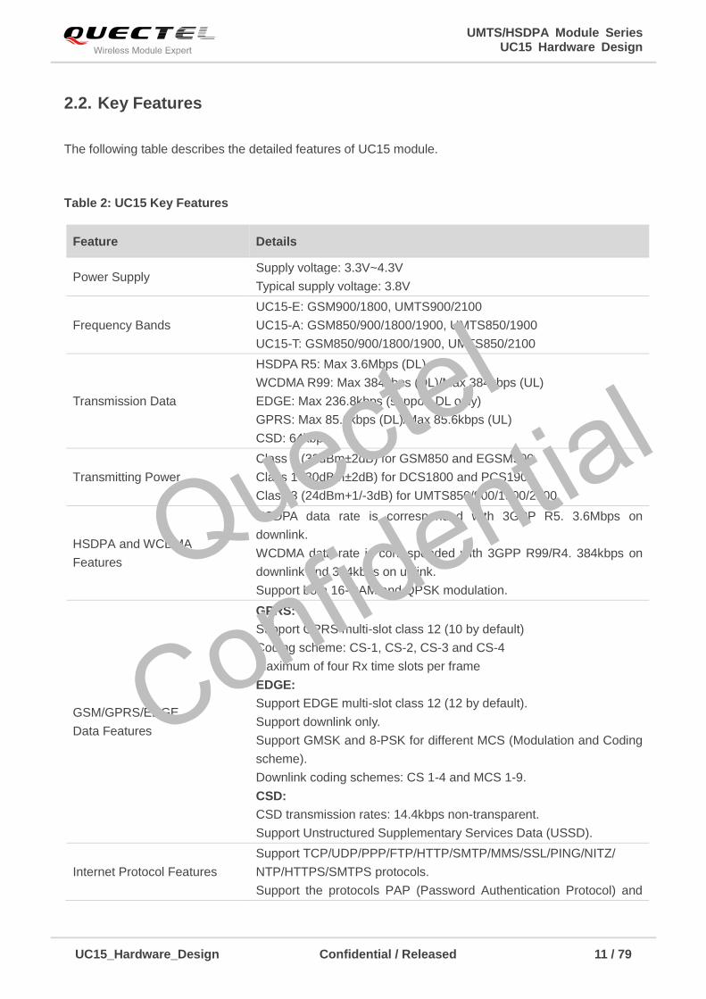
2.2. Key Features
The following table describes the detailed features of UC15 module.
Table 2: UC15 Key Features
Feature Details
Power Supply Supply voltage: 3.3V~4.3V
Typical supply voltage: 3.8V
Frequency Bands
UC15-E: GSM900/1800, UMTS900/2100
UC15-A: GSM850/900/1800/1900, UMTS850/1900
UC15-T: GSM850/900/1800/1900, UMTS850/2100
Transmission Data
HSDPA R5: Max 3.6Mbps (DL)
WCDMA R99: Max 384kbps (DL)/Max 384kbps (UL)
EDGE: Max 236.8kbps (support DL only)
GPRS: Max 85.6kbps (DL)/Max 85.6kbps (UL)
CSD: 64kbps
Transmitting Power
Class 4 (33dBm±2dB) for GSM850 and EGSM900
Class 1 (30dBm±2dB) for DCS1800 and PCS1900
Class 3 (24dBm+1/-3dB) for UMTS850/900/1900/2100
HSDPA and WCDMA
Features
HSDPA data rate is corresponded with 3GPP R5. 3.6Mbps on
downlink.
WCDMA data rate is corresponded with 3GPP R99/R4. 384kbps on
downlink and 384kbps on uplink.
Support both 16-QAM and QPSK modulation.
GSM/GPRS/EDGE
Data Features
GPRS:
Support GPRS multi-slot class 12 (10 by default)
Coding scheme: CS-1, CS-2, CS-3 and CS-4
Maximum of four Rx time slots per frame
EDGE:
Support EDGE multi-slot class 12 (12 by default).
Support downlink only.
Support GMSK and 8-PSK for different MCS (Modulation and Coding
scheme).
Downlink coding schemes: CS 1-4 and MCS 1-9.
CSD:
CSD transmission rates: 14.4kbps non-transparent.
Support Unstructured Supplementary Services Data (USSD).
Internet Protocol Features
Support TCP/UDP/PPP/FTP/HTTP/SMTP/MMS/SSL/PING/NITZ/
NTP/HTTPS/SMTPS protocols.
Support the protocols PAP (Password Authentication Protocol) and
Quectel
Confidential
UMTS/HSDPA Module Series UC15 Hardware Design
UC15_Hardware_Design Confidential / Released 12 / 79
CHAP (Challenge Handshake Authentication Protocol) usually used
for PPP connections.
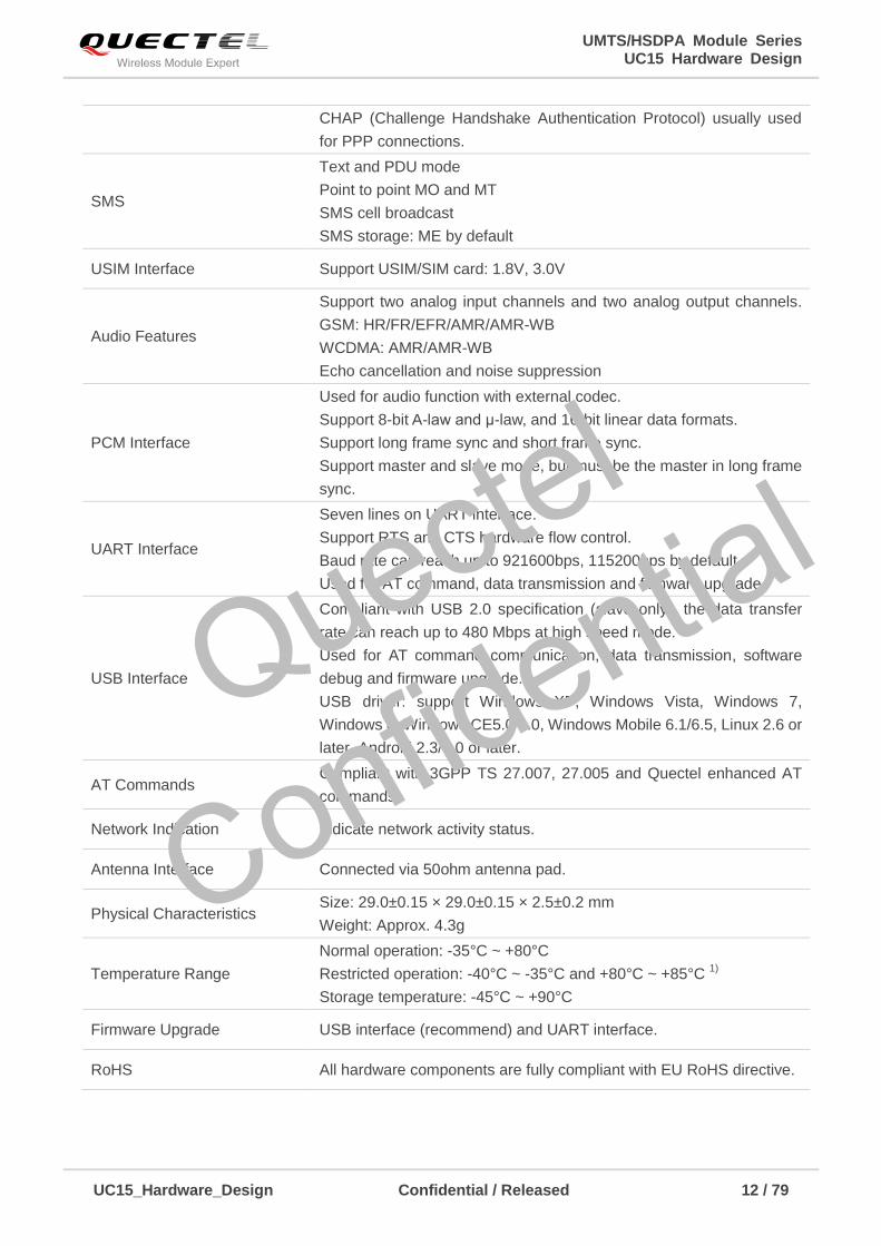
SMS
Text and PDU mode
Point to point MO and MT
SMS cell broadcast
SMS storage: ME by default
USIM Interface Support USIM/SIM card: 1.8V, 3.0V
Audio Features
Support two analog input channels and two analog output channels.
GSM: HR/FR/EFR/AMR/AMR-WB
WCDMA: AMR/AMR-WB
Echo cancellation and noise suppression
PCM Interface
Used for audio function with external codec.
Support 8-bit A-law and μ-law, and 16-bit linear data formats.
Support long frame sync and short frame sync.
Support master and slave mode, but must be the master in long frame
sync.
UART Interface
Seven lines on UART interface.
Support RTS and CTS hardware flow control.
Baud rate can reach up to 921600bps, 115200bps by default.
Used for AT command, data transmission and firmware upgrade.
USB Interface
Compliant with USB 2.0 specification (slave only), the data transfer
rate can reach up to 480 Mbps at high speed mode.
Used for AT command communication, data transmission, software
debug and firmware upgrade.
USB driver: support Windows XP, Windows Vista, Windows 7,
Windows 8, Windows CE5.0/6.0, Windows Mobile 6.1/6.5, Linux 2.6 or
later, Android 2.3/4.0 or later.
AT Commands Compliant with 3GPP TS 27.007, 27.005 and Quectel enhanced AT
commands.
Network Indication Indicate network activity status.
Antenna Interface Connected via 50ohm antenna pad.
Physical Characteristics Size: 29.0±0.15 × 29.0±0.15 × 2.5±0.2 mm
Weight: Approx. 4.3g
Temperature Range
Normal operation: -35°C ~ +80°C
Restricted operation: -40°C ~ -35°C and +80°C ~ +85°C 1)
Storage temperature: -45°C ~ +90°C
Firmware Upgrade USB interface (recommend) and UART interface.
RoHS All hardware components are fully compliant with EU RoHS directive.
Quectel
Confidential
UMTS/HSDPA Module Series UC15 Hardware Design
UC15_Hardware_Design Confidential / Released 13 / 79
“1)
” means when the module works within this temperature range, RF performance might degrade. For
example, the frequency error or the phase error would increase.
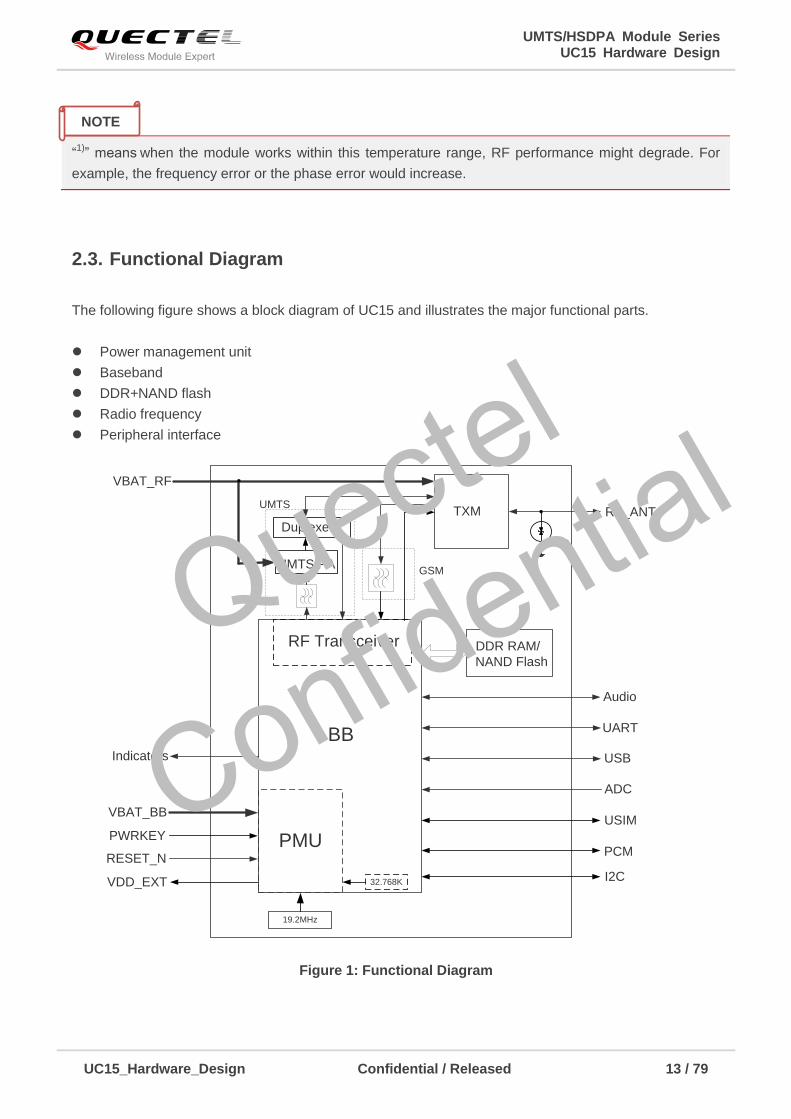
2.3. Functional Diagram
The following figure shows a block diagram of UC15 and illustrates the major functional parts.
Power management unit
Baseband
DDR+NAND flash
Radio frequency
Peripheral interface
PWRKEY
RESET_N
19.2MHz
BB
TXM
DDR RAM/
RF_ANT
USIM
ADC
UART
VBAT_BB
USB
VBAT_RF
GSM
UMTS
NAND Flash
Audio
PMU
VDD_EXT
RF Transceiver
UMTS PA
32.768K
ESD
Duplexer
Indicators
PCM
I2C
Figure 1: Functional Diagram
NOTE
Quectel
Confidential
UMTS/HSDPA Module Series UC15 Hardware Design
UC15_Hardware_Design Confidential / Released 14 / 79
2.4. Evaluation Board
In order to help you to develop applications with UC15, Quectel supplies an evaluation board (EVB),
RS-232 to USB cable, USB data cable, power adapter, earphone, antenna and other peripherals to
control or test the module. For details, please refer to document [2].
Quectel
Confidential
UMTS/HSDPA Module Series UC15 Hardware Design
UC15_Hardware_Design Confidential / Released 15 / 79
3 Application Interface
3.1. General Description
UC15 is equipped with a 68-pin 1.3mm pitch SMT pads plus 40-pin ground pads and reserved pads that
connect to cellular application platform. Sub-interfaces included in these pads are described in details in
the following chapters:
Power supply
UART interface
Audio interface
PCM interface
USIM interface
USB interface
ADC interface
Indicator interface
Quectel
Confidential
UMTS/HSDPA Module Series UC15 Hardware Design
UC15_Hardware_Design Confidential / Released 16 / 79
3.2. Pin Assignment
The following figure shows the pin assignment of the UC15 module.
32
17
18
19
20
21
22
23
24
25
26
27
28
29
30
31
1
3
4
5
6
7
2
RESERVED
AP_READY
RESERVED
RESERVED
RESERVED
NETLIGHT
VDD_EXT
GND
GND
RESERVED
RESERVED
USIM_PRESENCE
USIM_VDD
USIM_DATA
USIM_CLK
USIM_RST
RESERVED
67
68
8
9
10
11
12
13
14
15
16
48
47
46
45
44
43
42
66
65
41
40
39
38
37
36
35
34
33
64
63
62
61
60
59
58
57
56
55
54
53
52
51
50
49
USIM_GND
RE
SE
T_
N
PW
RK
EY
AG
ND
*
SP
K2
P*
SP
K1
N*
SP
K1
P*
MIC
1P
*
MIC
1N
*
MIC
2P
*
MIC
2N
*
RE
SE
RV
ED
RE
SE
RV
ED
RE
SE
RV
ED
RE
SE
RV
ED
RE
SE
RV
ED
RE
SE
RV
ED
US
B_
VB
US
US
B_
DM
US
B_
DP
RX
D
TX
D
DT
R
RT
S
CT
S
DC
D RI
ST
AT
US
VB
AT
_B
B
VB
AT
_B
B
VB
AT
_R
F
VB
AT
_R
F
GN
D
GND
GND
RF_ANT
GND
RESERVED
GND
ADC1
I2C_SCL
I2C_SDA
PCM_SYNC*
PCM_CLK*
PCM_DIN*
PCM_DOUT*
RESERVED
ADC0
GND
GND
GND
69
70
71
72
73
74
75
76
77
78
79
80
96
97
98
102
103
107
108
99
100105
101106
859094
848993
828792
81869195
8388
Power USB UART USIM ANT AUDIO OTHERS
104
GND RESERVEDPCM
Figure 2: Pin Assignment (Top View)
1. Keep all RESERVED pins and unused pins unconnected.
2. GND pads 81~108 should be connected to ground in the design. RESERVED pads 69~80 are used
for factory test, they are unused in your design, you can ignore them and don't design them in
schematic and PCB decal.
3. “*” means these functions are only supported in Telematics version.
NOTES
Quectel
Confidential
UMTS/HSDPA Module Series UC15 Hardware Design
UC15_Hardware_Design Confidential / Released 17 / 79
3.3. Pin Description
The pin definition of UC15 is shown in table 4.
Table 3: IO Parameters Definition
Table 4: Pin Description
Type Description
IO Bidirectional input/output
DI Digital input
DO Digital output
PI Power input
PO Power output
AI Analog input
AO Analog output
Power Supply
Pin Name Pin No. I/O Description DC Characteristics Comment
VBAT_BB 52,53 PI
Power supply for
module baseband
part.
Vmax=4.3V
Vmin=3.3V
Vnorm=3.8V
It must be able to
provide sufficient
current up to 0.8A.
VBAT_RF 50,51 PI Power supply for
module RF part.
Vmax=4.3V
Vmin=3.3V
Vnorm=3.8V
It must be able to
provide sufficient
current in a
transmitting burst
which typically
rises to 2.0A.
VDD_EXT 7 PO Provide 2.6V for
external circuit.
Vnorm=2.6V
IOmax=100mA
It is recommend to
add a 2.2~4.7uF
bypass capacitor
when using this
pin for power
supply.
Quectel
Confidential
UMTS/HSDPA Module Series UC15 Hardware Design
UC15_Hardware_Design Confidential / Released 18 / 79
GND
42,44~49
65,67~68
,81~108
Ground
Turn On/Off
Pin Name Pin No. I/O Description DC Characteristics Comment
PWRKEY 18 DI Turn on/off the
module.
RPU≈200kΩ
VIHmax=2.1V
VIHmin=1.3V
VILmax=0.5V
Pull-up to 1.8V
internally.
RESET_N 17 DI Reset the module.
VIHmax=2.1V
VIHmin=1.3V
VILmax=0.5V
Pull-up to 1.8V
internally. If
unused, keep it
open.
Indication
Pin Name Pin No. I/O Description DC Characteristics Comment
STATUS 54 DO Indicate the module
operating status.
VOHmax=2.6V
VOHmin=2.15V
VOLmax=0.45V
2.6V power
domain, if unused,
keep it open.
NETLIGHT 6 DO
Indicate the module
network activity
status.
VOHmax=2.6V
VOHmin=2.15V
VOLmax=0.45V
2.6V power
domain, if unused,
keep it open.
USB Interface
Pin Name Pin No. I/O Description DC Characteristics Comment
USB_VBUS 64 PI USB detection.
Vmax=5.25V
Vmin=3.0V
Vnorm=5.0V
USB_DP 62 IO USB differential data
bus.
Compliant with USB 2.0
standard specification.
Require differential
impedance of 90Ω.
USB_DM 63 IO USB differential data
bus.
Compliant with USB 2.0
standard specification.
Require differential
impedance of 90Ω.
USIM Interface
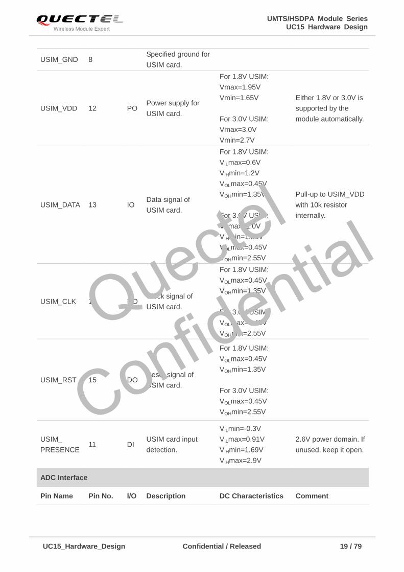
Pin Name Pin No. I/O Description DC Characteristics Comment
Quectel
Confidential
UMTS/HSDPA Module Series UC15 Hardware Design
UC15_Hardware_Design Confidential / Released 19 / 79
USIM_GND 8 Specified ground for
USIM card.
USIM_VDD 12 PO Power supply for
USIM card.
For 1.8V USIM:
Vmax=1.95V
Vmin=1.65V
For 3.0V USIM:
Vmax=3.0V
Vmin=2.7V
Either 1.8V or 3.0V is
supported by the
module automatically.
USIM_DATA 13 IO Data signal of
USIM card.
For 1.8V USIM:
VILmax=0.6V
VIHmin=1.2V
VOLmax=0.45V
VOHmin=1.35V
For 3.0V USIM:
VILmax=1.0V
VIHmin=1.95V
VOLmax=0.45V
VOHmin=2.55V
Pull-up to USIM_VDD
with 10k resistor
internally.
USIM_CLK 14 DO Clock signal of
USIM card.
For 1.8V USIM:
VOLmax=0.45V
VOHmin=1.35V
For 3.0V USIM:
VOLmax=0.45V
VOHmin=2.55V
USIM_RST 15 DO Reset signal of
USIM card.
For 1.8V USIM:
VOLmax=0.45V
VOHmin=1.35V
For 3.0V USIM:
VOLmax=0.45V
VOHmin=2.55V
USIM_
PRESENCE 11 DI
USIM card input
detection.
VILmin=-0.3V
VILmax=0.91V
VIHmin=1.69V
VIHmax=2.9V
2.6V power domain. If
unused, keep it open.
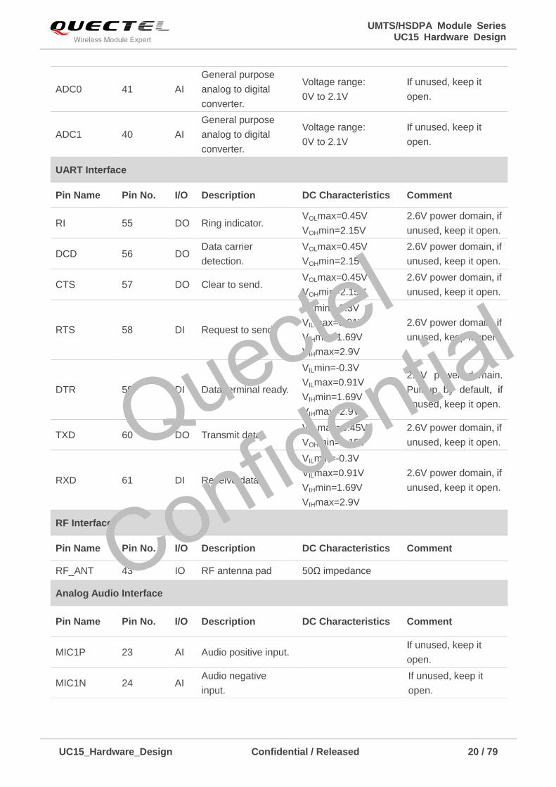
ADC Interface
Pin Name Pin No. I/O Description DC Characteristics Comment
Quectel
Confidential
UMTS/HSDPA Module Series UC15 Hardware Design
UC15_Hardware_Design Confidential / Released 20 / 79
ADC0 41 AI
General purpose
analog to digital
converter.
Voltage range:
0V to 2.1V
If unused, keep it
open.
ADC1 40 AI
General purpose
analog to digital
converter.
Voltage range:
0V to 2.1V
If unused, keep it
open.
UART Interface
Pin Name Pin No. I/O Description DC Characteristics Comment
RI 55 DO Ring indicator. VOLmax=0.45V
VOHmin=2.15V
2.6V power domain, if
unused, keep it open.
DCD 56 DO Data carrier
detection.
VOLmax=0.45V
VOHmin=2.15V
2.6V power domain, if
unused, keep it open.
CTS 57 DO Clear to send. VOLmax=0.45V
VOHmin=2.15V
2.6V power domain, if
unused, keep it open.
RTS 58 DI Request to send.
VILmin=-0.3V
VILmax=0.91V
VIHmin=1.69V
VIHmax=2.9V
2.6V power domain, if
unused, keep it open.
DTR 59 DI Data terminal ready.
VILmin=-0.3V
VILmax=0.91V
VIHmin=1.69V
VIHmax=2.9V
2.6V power domain.
Pull-up by default, if
unused, keep it open.
TXD 60 DO Transmit data. VOLmax=0.45V
VOHmin=2.15V
2.6V power domain, if
unused, keep it open.
RXD 61 DI Receive data.
VILmin=-0.3V
VILmax=0.91V
VIHmin=1.69V
VIHmax=2.9V
2.6V power domain, if
unused, keep it open.
RF Interface
Pin Name Pin No. I/O Description DC Characteristics Comment
RF_ANT 43 IO RF antenna pad 50Ω impedance
Analog Audio Interface
Pin Name Pin No. I/O Description DC Characteristics Comment
MIC1P 23 AI Audio positive input. If unused, keep it
open.
MIC1N 24 AI Audio negative
input.
If unused, keep it
open.
Quectel
Confidential
UMTS/HSDPA Module Series UC15 Hardware Design
UC15_Hardware_Design Confidential / Released 21 / 79
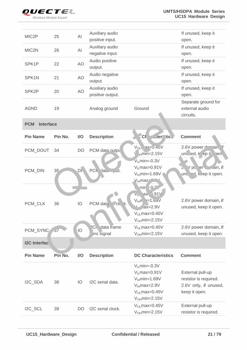
MIC2P 25 AI Auxiliary audio
positive input.
If unused, keep it
open.
MIC2N 26 AI Auxiliary audio
negative input.
If unused, keep it
open.
SPK1P 22 AO Audio positive
output.
If unused, keep it
open.
SPK1N 21 AO Audio negative
output.
If unused, keep it
open.
SPK2P 20 AO Auxiliary audio
positive output.
If unused, keep it
open.
AGND 19 Analog ground Ground
Separate ground for
external audio
circuits.
PCM Interface
Pin Name Pin No. I/O Description DC Characteristics Comment
PCM_DOUT 34 DO PCM data output. VOLmax=0.45V
VOHmin=2.15V
2.6V power domain, if
unused, keep it open.
PCM_DIN 35 DI PCM data input.
VILmin=-0.3V
VILmax=0.91V
VIHmin=1.69V
VIHmax=2.9V
2.6V power domain, if
unused, keep it open.
PCM_CLK 36 IO PCM data bit clock.
VILmin=-0.3V
VILmax=0.91V
VIHmin=1.69V
VIHmax=2.9V
VOLmax=0.45V
VOHmin=2.15V
2.6V power domain, if
unused, keep it open.
PCM_SYNC 37 IO PCM data frame
sync signal
VOLmax=0.45V
VOHmin=2.15V
2.6V power domain, if
unused, keep it open.
I2C Interface
Pin Name Pin No. I/O Description DC Characteristics Comment
I2C_SDA 38 IO I2C serial data.
VILmin=-0.3V
VILmax=0.91V
VIHmin=1.69V
VIHmax=2.9V
VOLmax=0.45V
VOHmin=2.15V
External pull-up
resistor is required.
2.6V only, if unused,
keep it open.
I2C_SCL 39 DO I2C serial clock. VOLmax=0.45V
VOHmin=2.15V
External pull-up
resistor is required.
Quectel
Confidential
UMTS/HSDPA Module Series UC15 Hardware Design
UC15_Hardware_Design Confidential / Released 22 / 79
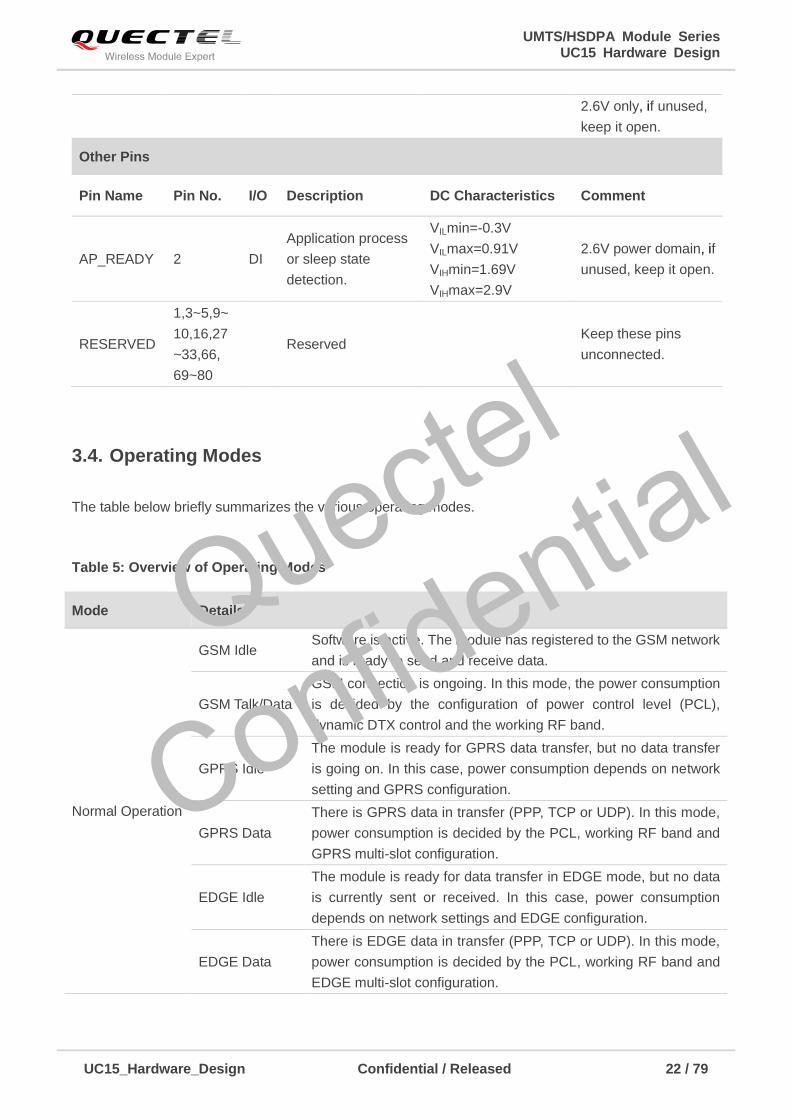
3.4. Operating Modes
The table below briefly summarizes the various operating modes.
Table 5: Overview of Operating Modes
2.6V only, if unused,
keep it open.
Other Pins
Pin Name Pin No. I/O Description DC Characteristics Comment
AP_READY 2 DI
Application process
or sleep state
detection.
VILmin=-0.3V
VILmax=0.91V
VIHmin=1.69V
VIHmax=2.9V
2.6V power domain, if
unused, keep it open.
RESERVED
1,3~5,9~
10,16,27
~33,66,
69~80
Reserved Keep these pins
unconnected.
Mode Details
Normal Operation
GSM Idle Software is active. The module has registered to the GSM network
and is ready to send and receive data.
GSM Talk/Data
GSM connection is ongoing. In this mode, the power consumption
is decided by the configuration of power control level (PCL),
dynamic DTX control and the working RF band.
GPRS Idle
The module is ready for GPRS data transfer, but no data transfer
is going on. In this case, power consumption depends on network
setting and GPRS configuration.
GPRS Data
There is GPRS data in transfer (PPP, TCP or UDP). In this mode,
power consumption is decided by the PCL, working RF band and
GPRS multi-slot configuration.
EDGE Idle
The module is ready for data transfer in EDGE mode, but no data
is currently sent or received. In this case, power consumption
depends on network settings and EDGE configuration.
EDGE Data
There is EDGE data in transfer (PPP, TCP or UDP). In this mode,
power consumption is decided by the PCL, working RF band and
EDGE multi-slot configuration.
Quectel
Confidential
UMTS/HSDPA Module Series UC15 Hardware Design
UC15_Hardware_Design Confidential / Released 23 / 79
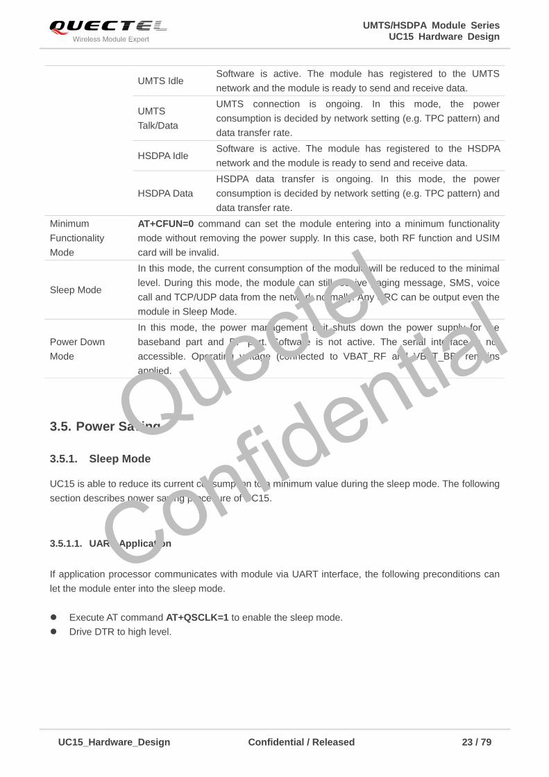
3.5. Power Saving
3.5.1. Sleep Mode
UC15 is able to reduce its current consumption to a minimum value during the sleep mode. The following
section describes power saving procedure of UC15.
3.5.1.1. UART Application
If application processor communicates with module via UART interface, the following preconditions can
let the module enter into the sleep mode.
Execute AT command AT+QSCLK=1 to enable the sleep mode.
Drive DTR to high level.
UMTS Idle Software is active. The module has registered to the UMTS
network and the module is ready to send and receive data.
UMTS
Talk/Data
UMTS connection is ongoing. In this mode, the power
consumption is decided by network setting (e.g. TPC pattern) and
data transfer rate.
HSDPA Idle Software is active. The module has registered to the HSDPA
network and the module is ready to send and receive data.
HSDPA Data
HSDPA data transfer is ongoing. In this mode, the power
consumption is decided by network setting (e.g. TPC pattern) and
data transfer rate.
Minimum
Functionality
Mode
AT+CFUN=0 command can set the module entering into a minimum functionality
mode without removing the power supply. In this case, both RF function and USIM
card will be invalid.
Sleep Mode
In this mode, the current consumption of the module will be reduced to the minimal
level. During this mode, the module can still receive paging message, SMS, voice
call and TCP/UDP data from the network normally. Any URC can be output even the
module in Sleep Mode.
Power Down
Mode
In this mode, the power management unit shuts down the power supply for the
baseband part and RF part. Software is not active. The serial interface is not
accessible. Operating voltage (connected to VBAT_RF and VBAT_BB) remains
applied.
Quectel
Confidential
UMTS/HSDPA Module Series UC15 Hardware Design
UC15_Hardware_Design Confidential / Released 24 / 79
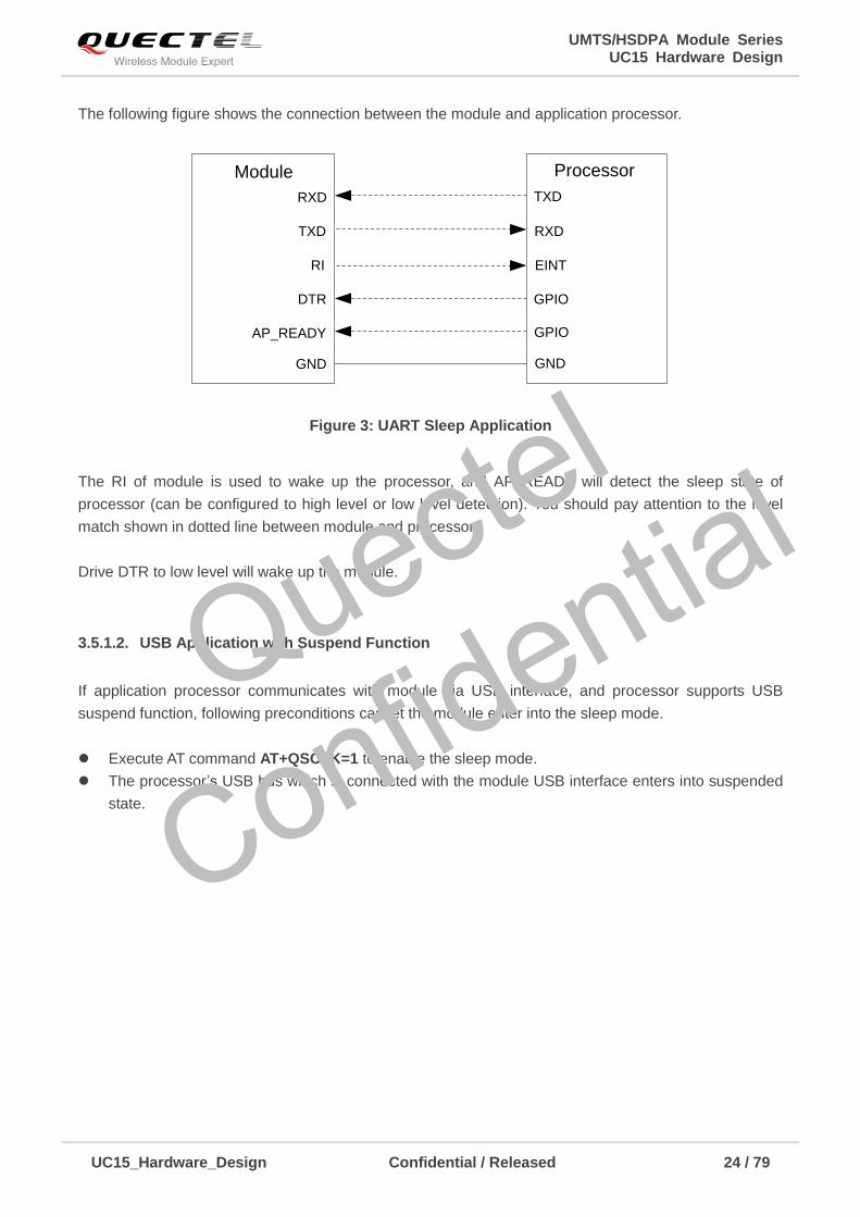
The following figure shows the connection between the module and application processor.
RXD
TXD
RI
DTR
AP_READY
TXD
RXD
EINT
GPIO
GPIO
Module Processor
GND GND
Figure 3: UART Sleep Application
The RI of module is used to wake up the processor, and AP_READY will detect the sleep state of
processor (can be configured to high level or low level detection). You should pay attention to the level
match shown in dotted line between module and processor.
Drive DTR to low level will wake up the module.
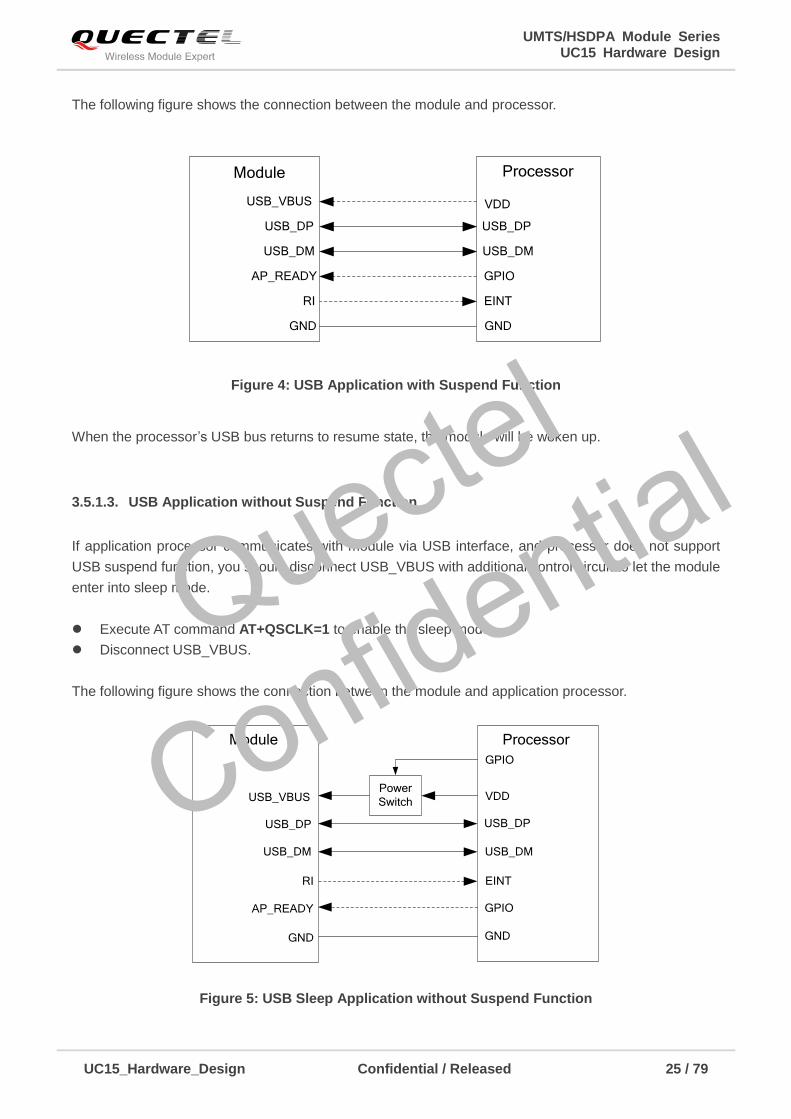
3.5.1.2. USB Application with Suspend Function
If application processor communicates with module via USB interface, and processor supports USB
suspend function, following preconditions can let the module enter into the sleep mode.
Execute AT command AT+QSCLK=1 to enable the sleep mode.
The processor’s USB bus which is connected with the module USB interface enters into suspended
state.
Quectel
Confidential
UMTS/HSDPA Module Series UC15 Hardware Design
UC15_Hardware_Design Confidential / Released 25 / 79
The following figure shows the connection between the module and processor.
USB_VBUS
USB_DP
USB_DM
AP_READY
VDD
USB_DP
USB_DM
GPIO
Module Processor
GND GND
RI EINT
Figure 4: USB Application with Suspend Function
When the processor’s USB bus returns to resume state, the module will be woken up.
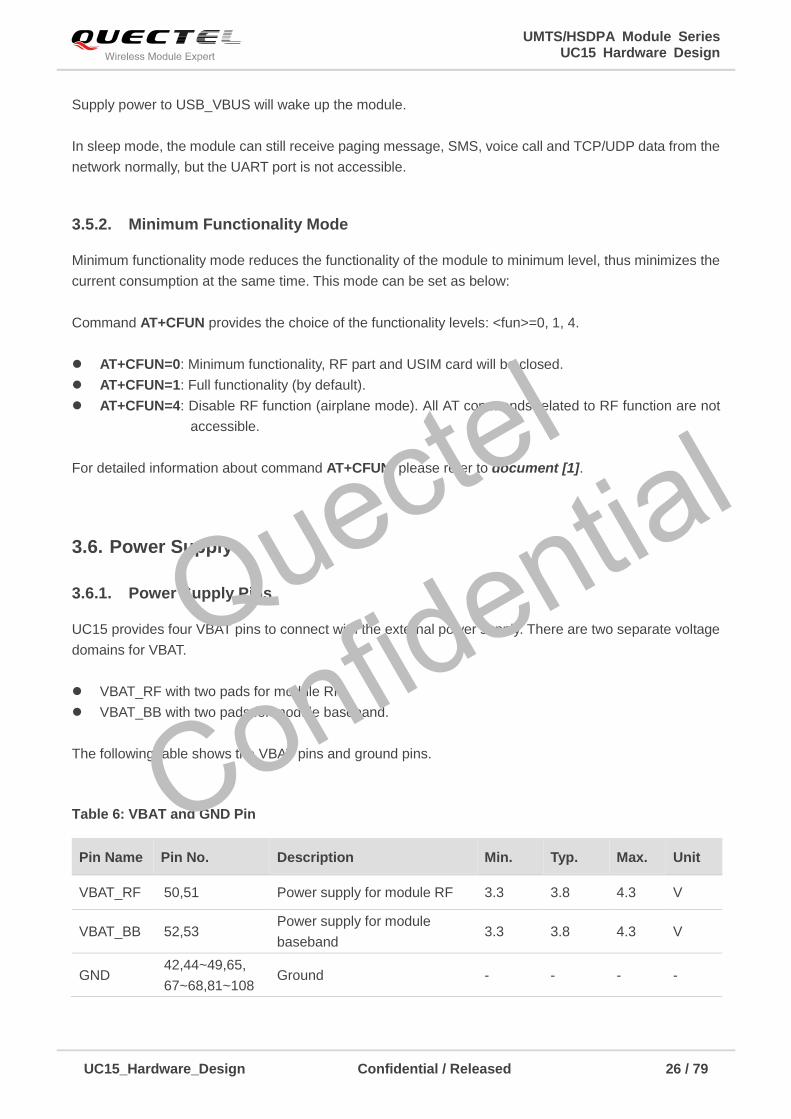
3.5.1.3. USB Application without Suspend Function
If application processor communicates with module via USB interface, and processor does not support
USB suspend function, you should disconnect USB_VBUS with additional control circuit to let the module
enter into sleep mode.
Execute AT command AT+QSCLK=1 to enable the sleep mode.
Disconnect USB_VBUS.
The following figure shows the connection between the module and application processor.
USB_VBUS
USB_DP
USB_DM
AP_READY
VDD
USB_DP
USB_DM
GPIO
Module Processor
RI EINT
Power
Switch
GPIO
GND GND
Figure 5: USB Sleep Application without Suspend Function
Quectel
Confidential
UMTS/HSDPA Module Series UC15 Hardware Design
UC15_Hardware_Design Confidential / Released 26 / 79
Supply power to USB_VBUS will wake up the module.
In sleep mode, the module can still receive paging message, SMS, voice call and TCP/UDP data from the
network normally, but the UART port is not accessible.
3.5.2. Minimum Functionality Mode
Minimum functionality mode reduces the functionality of the module to minimum level, thus minimizes the
current consumption at the same time. This mode can be set as below:
Command AT+CFUN provides the choice of the functionality levels: <fun>=0, 1, 4.
AT+CFUN=0: Minimum functionality, RF part and USIM card will be closed.
AT+CFUN=1: Full functionality (by default).
AT+CFUN=4: Disable RF function (airplane mode). All AT commands related to RF function are not
accessible.
For detailed information about command AT+CFUN, please refer to document [1].
3.6. Power Supply
3.6.1. Power Supply Pins
UC15 provides four VBAT pins to connect with the external power supply. There are two separate voltage
domains for VBAT.
VBAT_RF with two pads for module RF.
VBAT_BB with two pads for module baseband.
The following table shows the VBAT pins and ground pins.
Table 6: VBAT and GND Pin
Pin Name Pin No. Description Min. Typ. Max. Unit
VBAT_RF 50,51 Power supply for module RF 3.3 3.8 4.3 V
VBAT_BB 52,53 Power supply for module
baseband 3.3 3.8 4.3 V
GND 42,44~49,65,
67~68,81~108 Ground - - - -
Quectel
Confidential
UMTS/HSDPA Module Series UC15 Hardware Design
UC15_Hardware_Design Confidential / Released 27 / 79
3.6.2. Decrease Voltage Drop
The power supply range of the module is 3.3~4.3V. Because of the voltage drop during the transmitting
time, a bypass capacitor of about 100µF with low ESR should be used. Multi-layer ceramic chip (MLCC)
capacitor can provide the best combination of low ESR. Three ceramic capacitors (100nF, 33pF, 10pF)
are recommended to be applied to the VBAT pins. The capacitors should be placed close to the VBAT
pins of UC15. The following figure shows star structure of the power supply.
The main power supply from an external application should be a single voltage source and has to be
expanded to two sub paths with star structure. In addition, in order to get a stable power source, it is
suggested to use a zener diode of which reverse zener voltage is 5.1V and dissipation power is more than
0.5W.
Module
VBAT_RF
VBAT_BB
VBAT
C1
100uF
C6
100nF
C7
33pF
C8
10pF
++
C2
100nF
C5
100uF
C3
33pF
C4
10pF
D1
5.1V
Figure 6: Star Structure of the Power Supply
Please pay special attention to the power supply design for applications. Make sure the input voltage will
never drop below 3.3V. If the voltage drops below 3.3V, the module will turn into unnormal state. The PCB
traces from the VBAT pins to the power source must be wide enough to ensure that there is not too much
voltage drop occurs in the transmitting procedure. The width of VBAT_BB trace should be no less than
1mm, and the width of VBAT_RF trace should be no less than 2mm, and the principle of the VBAT trace is
the longer, the wider.
3.6.3. Reference Design for Power Supply
The power design for the module is very important, since the performance of power supply for the module
largely depends on the power source. The power supply is capable of providing the sufficient current up to
2A at least. If the voltage drop between the input and output is not too high, it is suggested to use a LDO
to supply power for module. If there is a big voltage difference between the input source and the desired
output (VBAT), a buck converter is preferred to be used as a power supply.
Quectel
Confidential
UMTS/HSDPA Module Series UC15 Hardware Design
UC15_Hardware_Design Confidential / Released 28 / 79
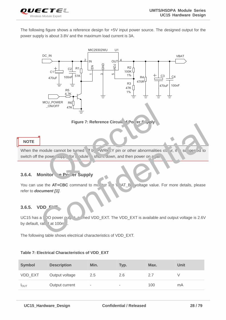
The following figure shows a reference design for +5V input power source. The designed output for the
power supply is about 3.8V and the maximum load current is 3A.
DC_IN
C1C2
MIC29302WU U1
IN OUT
EN
GN
D
AD
J
2 4
1 3 5
VBAT
100nF C3
470uF
C4
100nF
R2
100K
47K
R3
470uF
470R
51K R4
R1
1%
1%
MCU_POWER
_ON/OFF 47K
4.7KR5
R6
Figure 7: Reference Circuit of Power Supply
When the module cannot be turned off by PWRKEY pin or other abnormalities occur, it is suggested to
switch off the power supply for module to shut it down, and then power on again.
3.6.4. Monitor the Power Supply
You can use the AT+CBC command to monitor the VBAT_BB voltage value. For more details, please
refer to document [1].
3.6.5. VDD_EXT
UC15 has a LDO power output, named VDD_EXT. The VDD_EXT is available and output voltage is 2.6V
by default, rated at 100mA.
The following table shows electrical characteristics of VDD_EXT.
Table 7: Electrical Characteristics of VDD_EXT
Symbol Description Min. Typ. Max. Unit
VDD_EXT Output voltage 2.5 2.6 2.7 V
IOUT Output current - - 100 mA
NOTE
Quectel
Confidential
UMTS/HSDPA Module Series UC15 Hardware Design
UC15_Hardware_Design Confidential / Released 29 / 79
3.7. Turn on and off Scenarios
3.7.1. Turn on Module by PWRKEY Pin
The following table shows the pin definition of PWRKEY.
Table 8: PWRKEY Pin Description
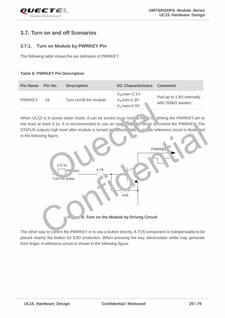
When UC15 is in power down mode, it can be turned on to normal mode by driving the PWRKEY pin to
low level at least 0.1s. It is recommended to use an open collector driver to control the PWRKEY. The
STATUS outputs high level after module is turned on successfully. A simple reference circuit is illustrated
in the following figure.
Turn on pulse
PWRKEY
4.7K
47K
≥ 0.1s
Figure 8: Turn on the Module by Driving Circuit
The other way to control the PWRKEY is to use a button directly. A TVS component is indispensable to be
placed nearby the button for ESD protection. When pressing the key, electrostatic strike may generate
from finger. A reference circuit is shown in the following figure.
Pin Name Pin No. Description DC Characteristics Comment
PWRKEY 18 Turn on/off the module
VIHmax=2.1V
VIHmin=1.3V
VILmax=0.5V
Pull-up to 1.8V internally
with 200kΩ resistor.
Quectel
Confidential
UMTS/HSDPA Module Series UC15 Hardware Design
UC15_Hardware_Design Confidential / Released 30 / 79
PWRKEY
S1
Close to S1
TVS
Figure 9: Turn on the Module by Keystroke
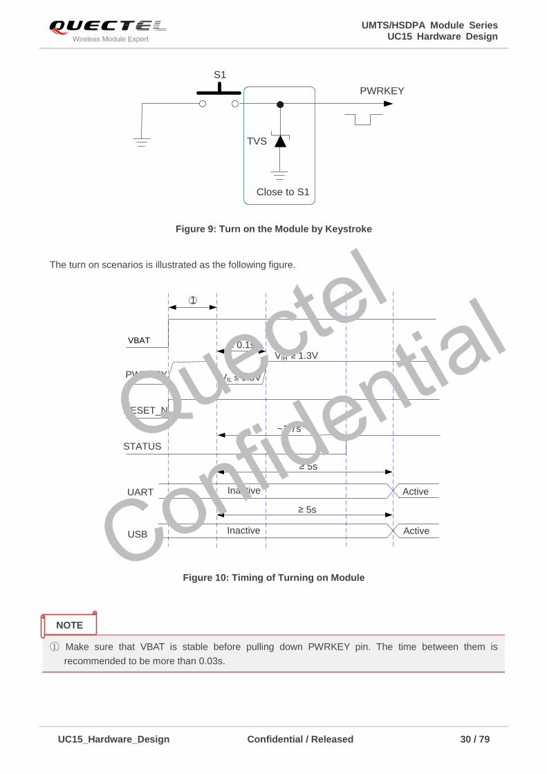
The turn on scenarios is illustrated as the following figure.
VIL ≤ 0.5V
VIH ≥ 1.3V
VBAT
PWRKEY
≥ 0.1s
InactiveUART Active
1
≥ 5s
RESET_N
STATUS
~1.7s
Inactive ActiveUSB
≥ 5s
Figure 10: Timing of Turning on Module
① Make sure that VBAT is stable before pulling down PWRKEY pin. The time between them is
recommended to be more than 0.03s.
NOTE
Quectel
Confidential
UMTS/HSDPA Module Series UC15 Hardware Design
UC15_Hardware_Design Confidential / Released 31 / 79
3.7.2. Turn off Module
The following procedures can be used to turn off the module:
Normal power down procedure: Turn off the module by PWRKEY pin.
Normal power down procedure: Turn off the module by command AT+QPOWD.
Automatic shutdown: Turn off the module automatically if under-voltage or over-voltage is detected.
3.7.2.1. Turn off Module by PWRKEY Pin
Drive the PWRKEY to low level at least 0.6s, the module will execute power-down procedure after
PWRKEY is released. The power-down scenario is illustrated as the following figure.
VBAT
PWRKEY
Log off network about 1s to 60s≥ 0.6s
RUNNING Power-down Procedure OFFModuleStatus
STATUS
Figure 11: Timing of Turning off Module
During power-down procedure, module will send out URC “NORMAL POWER DOWN” via URC port first,
then log off network and save important data. After logging off, module sends out “POWERED DOWN”
and shuts down the internal power supply. The power on VBAT pins are not allowed to be switched off
before the URC “POWERED DOWN” is output to avoid data loss. If module is not logged off within 60s,
module will force to shut down internal power supply.
After that moment, the module enters into power down mode, no other AT commands can be executed.
3.7.2.2. Turn off Module by AT Command
It is also a safe way to use AT command AT+QPOWD to turn off the module, which is similar to the way of
turning off the module via PWRKEY Pin. Please refer to document [1] for details about the AT command
of AT+QPOWD.
Quectel
Confidential
UMTS/HSDPA Module Series UC15 Hardware Design
UC15_Hardware_Design Confidential / Released 32 / 79
3.7.2.3. Automatic Shutdown
The module will constantly monitor the voltage applied on the VBAT_BB, if the voltage ≤ 3.5V, the
following URC will be presented:
+QIND: “vbatt”,-1
If the voltage ≥ 4.21V, the following URC will be presented:
+QIND: “vbatt”,1
The uncritical voltage is 3.3V to 4.3V, If the voltage > 4.35V or < 3.2V, the module would automatically
shut down itself.
If the voltage < 3.2V, the following URC will be presented:
+QIND: “vbatt”,-2
If the voltage > 4.35V, the following URC will be presented:
+QIND: “vbatt”,2
The value of voltage threshold can be revised by AT command AT+QCFG=“vbatt”, refer to document
[1] for details.
3.8. Reset the Module
The RESET_N can be used to reset the module.
Table 9: RESET_N Pin Description
Pin Name Pin No. Description DC Characteristics Comment
RESET_N 17 Reset the module.
VIHmax=2.1V
VIHmin=1.3V
VILmax=0.5V
Pull-up to 1.8V internally.
If unused, keep it open.
NOTE
Quectel
Confidential
UMTS/HSDPA Module Series UC15 Hardware Design
UC15_Hardware_Design Confidential / Released 33 / 79
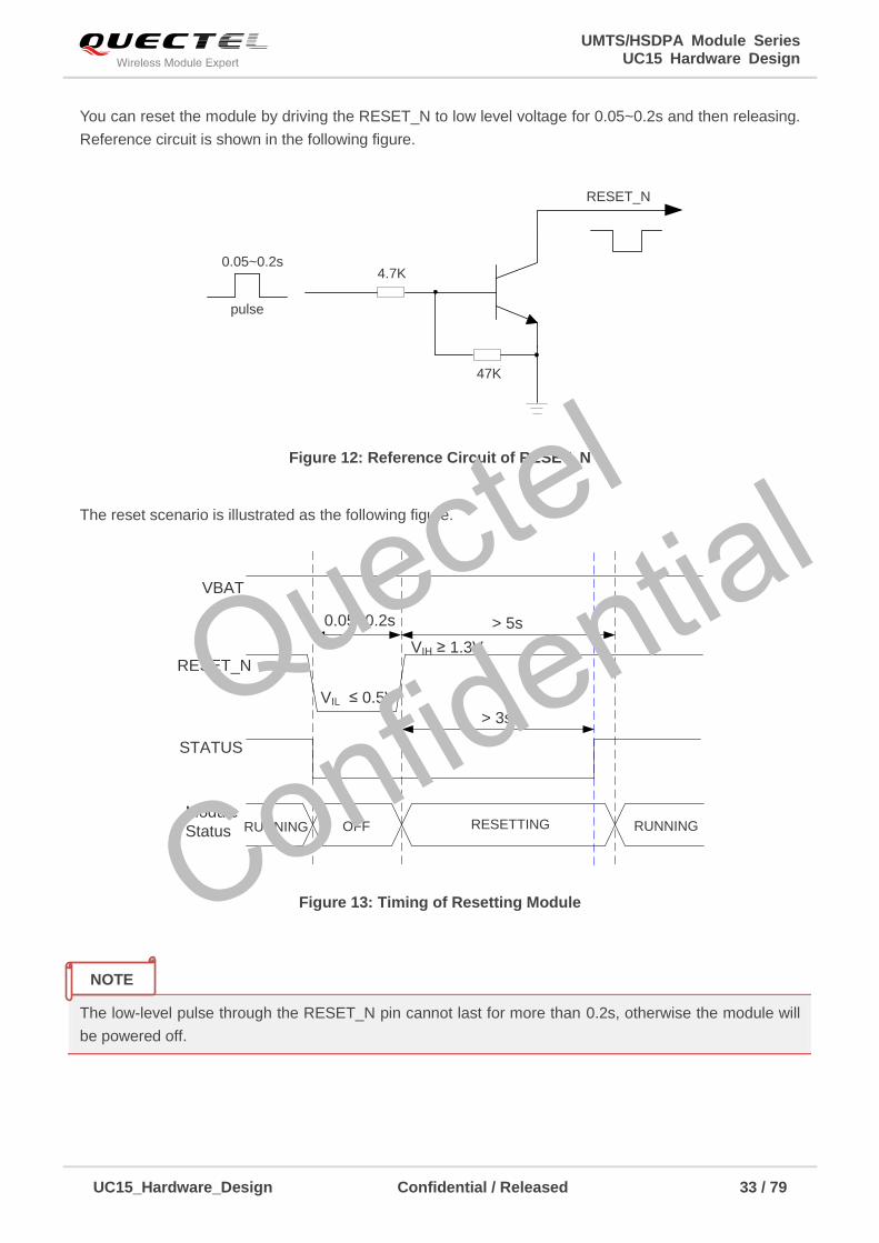
You can reset the module by driving the RESET_N to low level voltage for 0.05~0.2s and then releasing.
Reference circuit is shown in the following figure.
pulse
RESET_N
4.7K
47K
0.05~0.2s
Figure 12: Reference Circuit of RESET_N
The reset scenario is illustrated as the following figure.
VIL ≤ 0.5V
VIH ≥ 1.3V
VBAT
0.05~0.2s
RESETTING
RESET_N
RUNNING
> 5s
STATUS
> 3s
Module
Status RUNNING OFF
Figure 13: Timing of Resetting Module
The low-level pulse through the RESET_N pin cannot last for more than 0.2s, otherwise the module will
be powered off.
NOTE
Quectel
Confidential
UMTS/HSDPA Module Series UC15 Hardware Design
UC15_Hardware_Design Confidential / Released 34 / 79
3.9. UART Interface
The module provides one 7-wire UART interface, and is designed as the DCE (Data Communication
Equipment), following the traditional DCE-DTE (Data Terminal Equipment) connection. UART interface
supports 300, 600, 1200, 2400, 4800, 9600, 19200, 38400, 57600, 115200, 230400, 460800 and
921600bps baud rate. The default is 115200bps, please refer to document [1] about AT+IPR command
for details. This interface can be used for data transmission, AT communication and firmware upgrade.
Table 10: Pin Definition of the UART Interface
The logic levels are described in the following table.
Table 11: Logic Levels of Digital I/O
Pin Name Pin No. I/O Description Comment
RI 55 DO Ring indicator 2.6V power domain. If unused,
keep it open.
DCD 56 DO Data carrier detection 2.6V power domain. If unused,
keep it open.
CTS 57 DO Clear to send 2.6V power domain. If unused,
keep it open.
RTS 58 DI Request to send 2.6V power domain. If unused,
keep it open.
DTR 59 DI Data terminal ready 2.6V power domain. If unused,
keep it open.
TXD 60 DO Transmit data 2.6V power domain. If unused,
keep it open.
RXD 61 DI Receive data 2.6V power domain. If unused,
keep it open.
Parameter Min. Max. Unit
VIL -0.3 0.91 V
VIH 1.69 2.9 V
VOL 0 0.45 V
VOH 2.15 2.6 V
Quectel
Confidential
UMTS/HSDPA Module Series UC15 Hardware Design
UC15_Hardware_Design Confidential / Released 35 / 79
3.9.1. The Connection of UART
The connection between module and host via UART port is very flexible. Three connection ways are
illustrated as below.
UART port connection is shown as below when it is applied in modulation-demodulation.
TXD
RXD
RTS
CTS
DTR
DCD
RI
TXD
RXD
RTS
CTS
DTR
DCD
RING
Module
GND GND
PC
Figure 14: Connection of Full Functional UART Port
Three lines connection is shown as below.
TXD
RXD
GND
TXD
RXD
GND
Module MCU
Figure 15: Connection of Three Lines UART Port
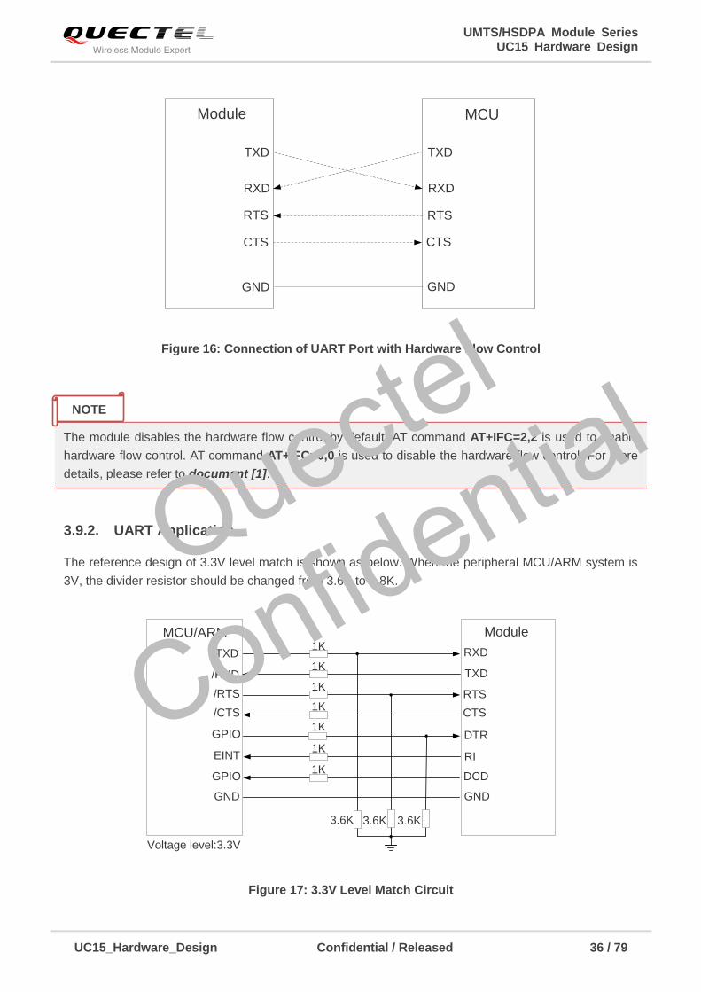
UART port with hardware flow control is shown as below. This connection will enhance the reliability of the
mass data communication.
Quectel
Confidential
UMTS/HSDPA Module Series UC15 Hardware Design
UC15_Hardware_Design Confidential / Released 36 / 79
RTS
CTS
RTS
CTS
GND
RXD
TXD TXD
RXD
GND
Module MCU
Figure 16: Connection of UART Port with Hardware Flow Control
The module disables the hardware flow control by default. AT command AT+IFC=2,2 is used to enable
hardware flow control. AT command AT+IFC=0,0 is used to disable the hardware flow control. For more
details, please refer to document [1].
3.9.2. UART Application
The reference design of 3.3V level match is shown as below. When the peripheral MCU/ARM system is
3V, the divider resistor should be changed from 3.6K to 6.8K.
MCU/ARM
/TXD
/RXD
1K
TXD
RXD
RTS
CTS
DTR
RI
/RTS
/CTS
GPIO
EINT
GPIO DCD
Module
1K
1K
Voltage level:3.3V
3.6K3.6K3.6K
1K
1K
1K
1K
GND GND
Figure 17: 3.3V Level Match Circuit
NOTE
Quectel
Confidential
UMTS/HSDPA Module Series UC15 Hardware Design
UC15_Hardware_Design Confidential / Released 37 / 79
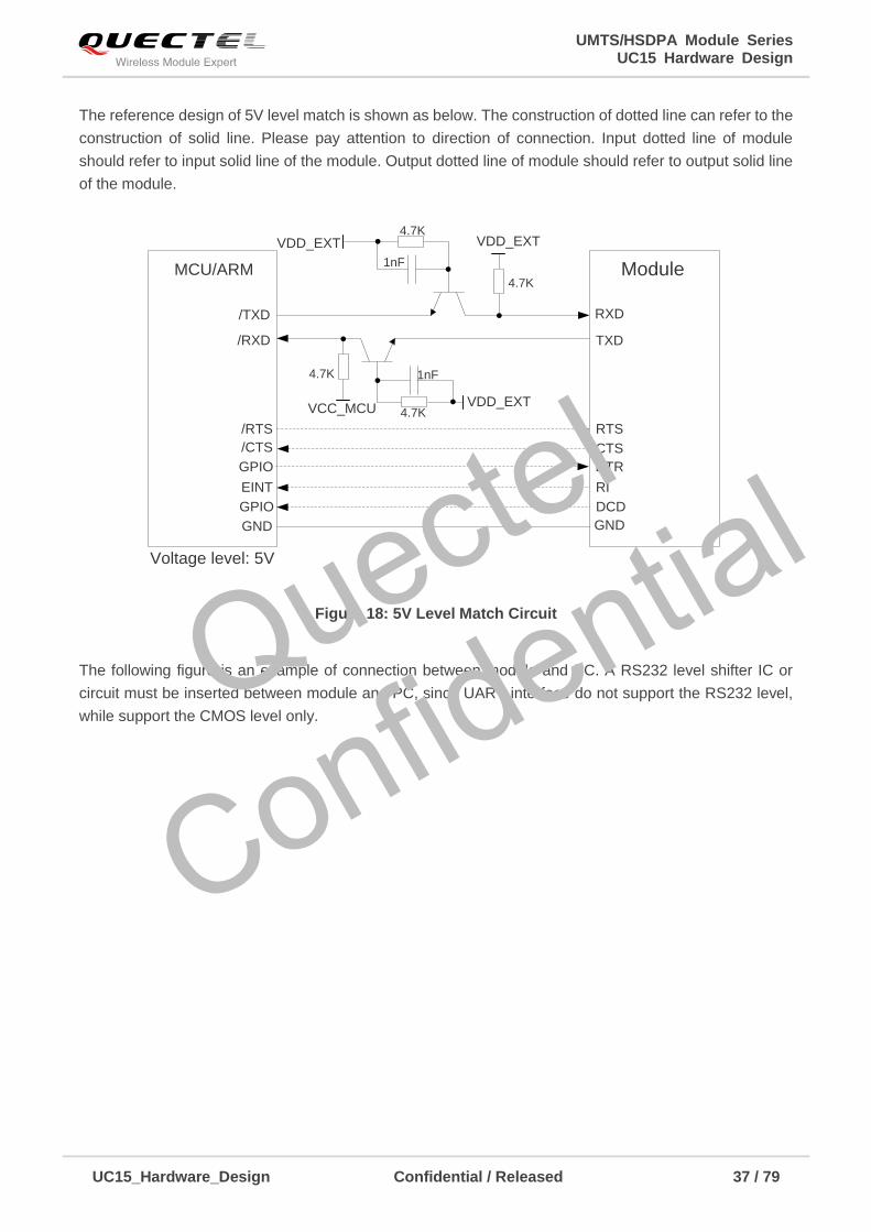
The reference design of 5V level match is shown as below. The construction of dotted line can refer to the
construction of solid line. Please pay attention to direction of connection. Input dotted line of module
should refer to input solid line of the module. Output dotted line of module should refer to output solid line
of the module.
MCU/ARM
/TXD
/RXD
VDD_EXT
4.7K
VCC_MCU 4.7K
4.7K
VDD_EXT
TXD
RXD
RTS
CTS
DTR
RI
/RTS
/CTS
GND
GPIO DCD
Module
GPIO
EINT
VDD_EXT
Voltage level: 5V
4.7K
GND
1nF
1nF
Figure 18: 5V Level Match Circuit
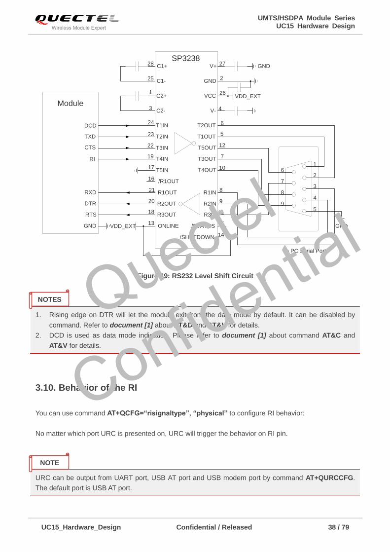
The following figure is an example of connection between module and PC. A RS232 level shifter IC or
circuit must be inserted between module and PC, since UART interface do not support the RS232 level,
while support the CMOS level only. Quectel
Confidential
UMTS/HSDPA Module Series UC15 Hardware Design
UC15_Hardware_Design Confidential / Released 38 / 79
TXD
RXD
RTS
CTS
DTR
RI
DCD
Module
GND
C1+
C1-
C2+
C2-
28
25
1
3
V+
VCC
GND
V-
VDD_EXT
27
2
26
4
T1IN
T2IN
T3IN
T4IN
R1IN
R2IN
R3IN
R1OUT
R2OUT
R3OUT
T1OUT
T2OUT
T5OUT
T3OUT
T4OUTT5IN
ONLINE /STATUS
/SHUTDOWN
SP3238
/R1OUT
24
23
22
19
17
16
21
20
18
13
14
10
6
7
5
12
8
9
11
15
1
2
3
4
5
6
7
8
9
GND
To PC Serial Port
GND
VDD_EXT
Figure 19: RS232 Level Shift Circuit
1. Rising edge on DTR will let the module exit from the data mode by default. It can be disabled by
command. Refer to document [1] about AT&D and AT&V for details.
2. DCD is used as data mode indication. Please refer to document [1] about command AT&C and
AT&V for details.
3.10. Behavior of the RI
You can use command AT+QCFG=“risignaltype”, “physical” to configure RI behavior:
No matter which port URC is presented on, URC will trigger the behavior on RI pin.
URC can be output from UART port, USB AT port and USB modem port by command AT+QURCCFG.
The default port is USB AT port.
NOTES
NOTE
Quectel
Confidential
UMTS/HSDPA Module Series UC15 Hardware Design
UC15_Hardware_Design Confidential / Released 39 / 79
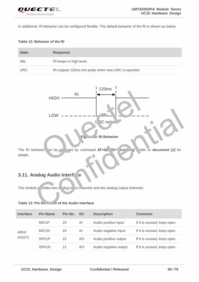
In additional, RI behavior can be configured flexible. The default behavior of the RI is shown as below.
Table 12: Behavior of the RI
HIGH
120ms
URC reports
LOW
RI
Figure 20: RI Behavior
The RI behavior can be changed by command AT+QCFG=“urc/ri/ring”, refer to document [1] for
details.
3.11. Analog Audio Interface
The module provides two analog input channels and two analog output channels.
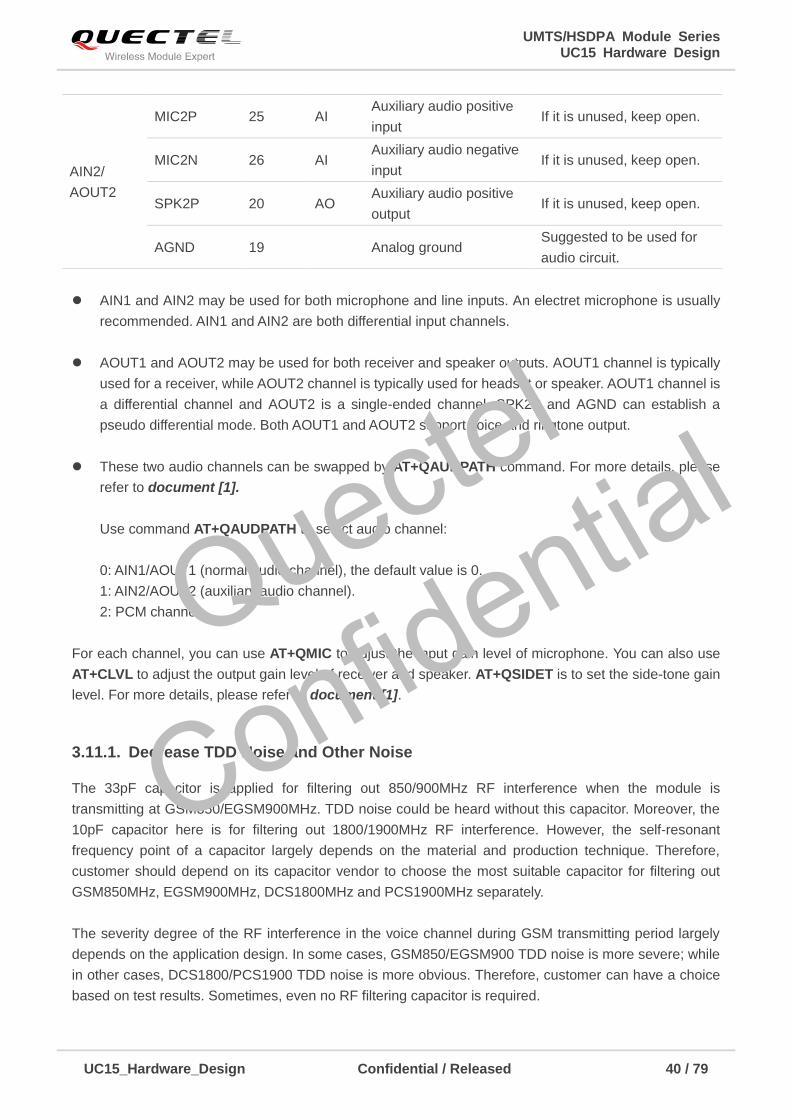
Table 13: Pin Definition of the Audio Interface
State Response
Idle RI keeps in high level.
URC RI outputs 120ms low pulse when new URC is reported.
Interface Pin Name Pin No. I/O Description Comment
AIN1/
AOUT1
MIC1P 23 AI Audio positive input If it is unused, keep open.
MIC1N 24 AI Audio negative input If it is unused, keep open.
SPK1P 22 AO Audio positive output If it is unused, keep open.
SPK1N 21 AO Audio negative output If it is unused, keep open.
Quectel
Confidential
UMTS/HSDPA Module Series UC15 Hardware Design
UC15_Hardware_Design Confidential / Released 40 / 79
AIN1 and AIN2 may be used for both microphone and line inputs. An electret microphone is usually
recommended. AIN1 and AIN2 are both differential input channels.
AOUT1 and AOUT2 may be used for both receiver and speaker outputs. AOUT1 channel is typically
used for a receiver, while AOUT2 channel is typically used for headset or speaker. AOUT1 channel is
a differential channel and AOUT2 is a single-ended channel. SPK2P and AGND can establish a
pseudo differential mode. Both AOUT1 and AOUT2 support voice and ringtone output.
These two audio channels can be swapped by AT+QAUDPATH command. For more details, please
refer to document [1].
Use command AT+QAUDPATH to select audio channel:
0: AIN1/AOUT1 (normal audio channel), the default value is 0.
1: AIN2/AOUT2 (auxiliary audio channel).
2: PCM channel.
For each channel, you can use AT+QMIC to adjust the input gain level of microphone. You can also use
AT+CLVL to adjust the output gain level of receiver and speaker. AT+QSIDET is to set the side-tone gain
level. For more details, please refer to document [1].
3.11.1. Decrease TDD Noise and Other Noise
The 33pF capacitor is applied for filtering out 850/900MHz RF interference when the module is
transmitting at GSM850/EGSM900MHz. TDD noise could be heard without this capacitor. Moreover, the
10pF capacitor here is for filtering out 1800/1900MHz RF interference. However, the self-resonant
frequency point of a capacitor largely depends on the material and production technique. Therefore,
customer should depend on its capacitor vendor to choose the most suitable capacitor for filtering out
GSM850MHz, EGSM900MHz, DCS1800MHz and PCS1900MHz separately.
The severity degree of the RF interference in the voice channel during GSM transmitting period largely
depends on the application design. In some cases, GSM850/EGSM900 TDD noise is more severe; while
in other cases, DCS1800/PCS1900 TDD noise is more obvious. Therefore, customer can have a choice
based on test results. Sometimes, even no RF filtering capacitor is required.
AIN2/
AOUT2
MIC2P 25 AI Auxiliary audio positive
input If it is unused, keep open.
MIC2N 26 AI Auxiliary audio negative
input If it is unused, keep open.
SPK2P 20 AO Auxiliary audio positive
output If it is unused, keep open.
AGND 19 Analog ground Suggested to be used for
audio circuit.
Quectel
Confidential
UMTS/HSDPA Module Series UC15 Hardware Design
UC15_Hardware_Design Confidential / Released 41 / 79
The capacitor which is used for filtering out RF noise should be close to audio interface. Audio alignment
should be as short as possible.
In order to decrease radio or other signal interference, the position of RF antenna should be kept away
from audio interface and audio alignment. Power alignment and audio alignment should not be parallel,
and power alignment should be far away from audio alignment.
The differential audio traces should be placed according to the differential signal layout rules.
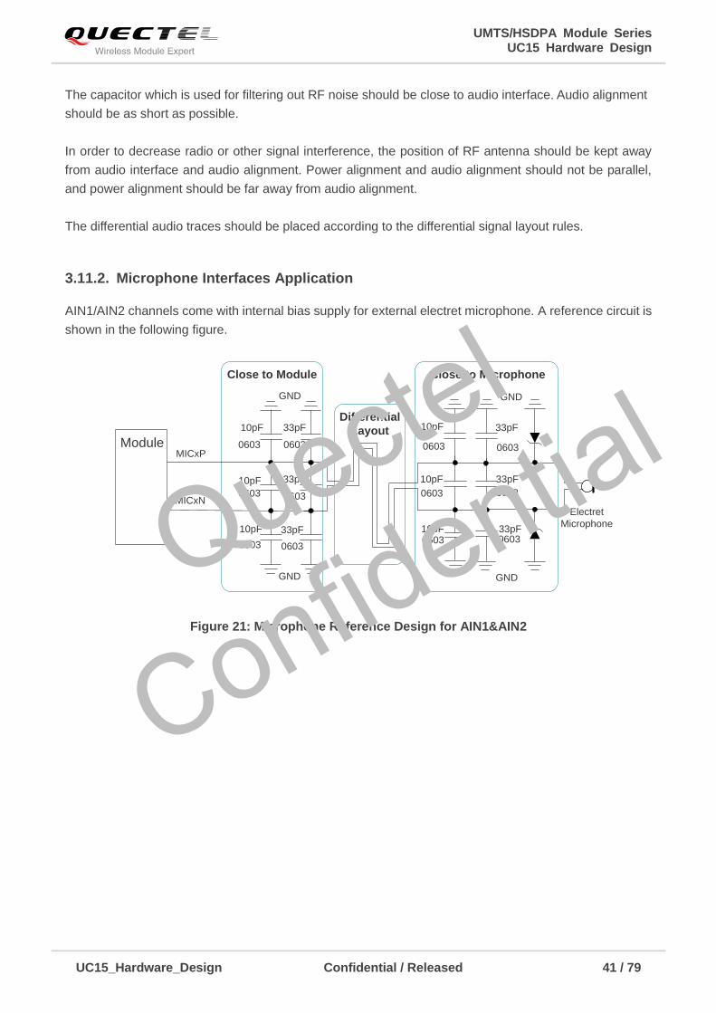
3.11.2. Microphone Interfaces Application
AIN1/AIN2 channels come with internal bias supply for external electret microphone. A reference circuit is
shown in the following figure.
MICxP
Differential
LayoutModule
10pF 33pF
33pF
33pF
Electret
Microphone
GND
GND
10pF
10pF10pF
Close to Module
MICxN
GND
10pF
10pF
0603
0603
0603
0603
0603
0603
0603
0603
0603
GND
33pF
0603
33pF
33pF
0603
0603
Close to Microphone
Figure 21: Microphone Reference Design for AIN1&AIN2
Quectel
Confidential
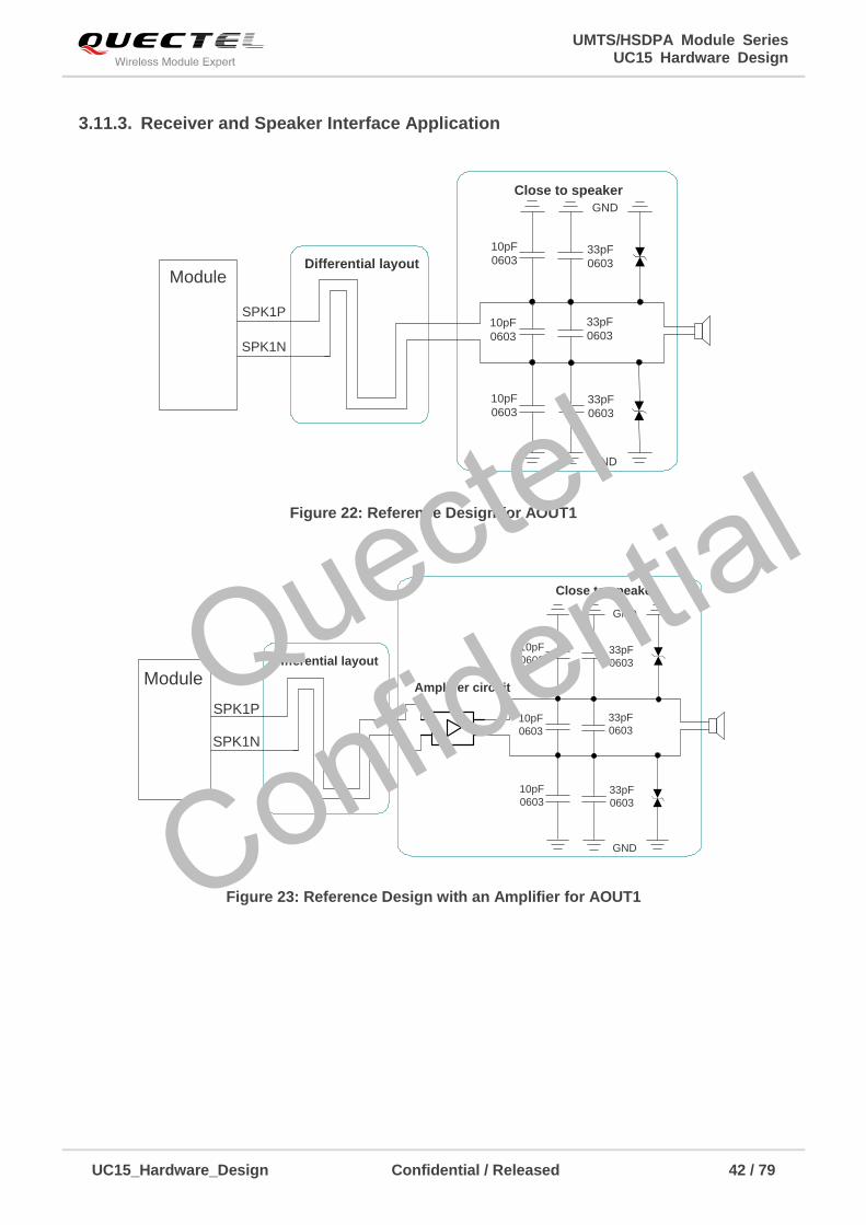
UMTS/HSDPA Module Series UC15 Hardware Design
UC15_Hardware_Design Confidential / Released 42 / 79
3.11.3. Receiver and Speaker Interface Application
SPK1P
SPK1N
Differential layoutModule
10pF
0603
GND
33pF
0603
33pF
0603
GND
10pF
0603
10pF
0603
33pF
0603
Close to speaker
Figure 22: Reference Design for AOUT1
SPK1P
SPK1N
Differential layout
Amplifier circuitModule
10pF
0603
Close to speaker
GND
33pF
0603
33pF
0603
GND
10pF
0603
10pF
0603
33pF
0603
Figure 23: Reference Design with an Amplifier for AOUT1
Quectel
Confidential
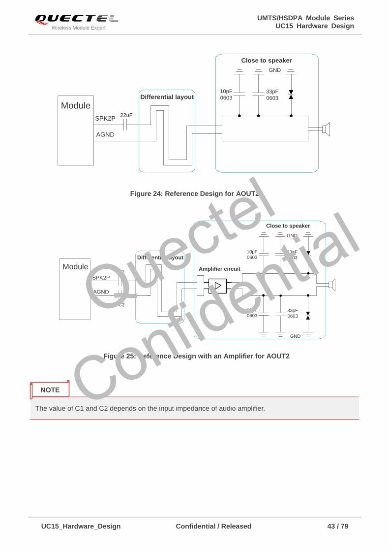
UMTS/HSDPA Module Series UC15 Hardware Design
UC15_Hardware_Design Confidential / Released 43 / 79
SPK2P
AGND
Differential layout
Module22uF
Close to speaker
GND
33pF
0603
10pF
0603
Figure 24: Reference Design for AOUT2
Module
SPK2P
AGND
Differential layout
Amplifier circuit
10pF
0603
Close to speaker
GND
C2
C1
33pF
0603
33pF
0603
GND
10pF
0603
Figure 25: Reference Design with an Amplifier for AOUT2
The value of C1 and C2 depends on the input impedance of audio amplifier.
NOTE
Quectel
Confidential
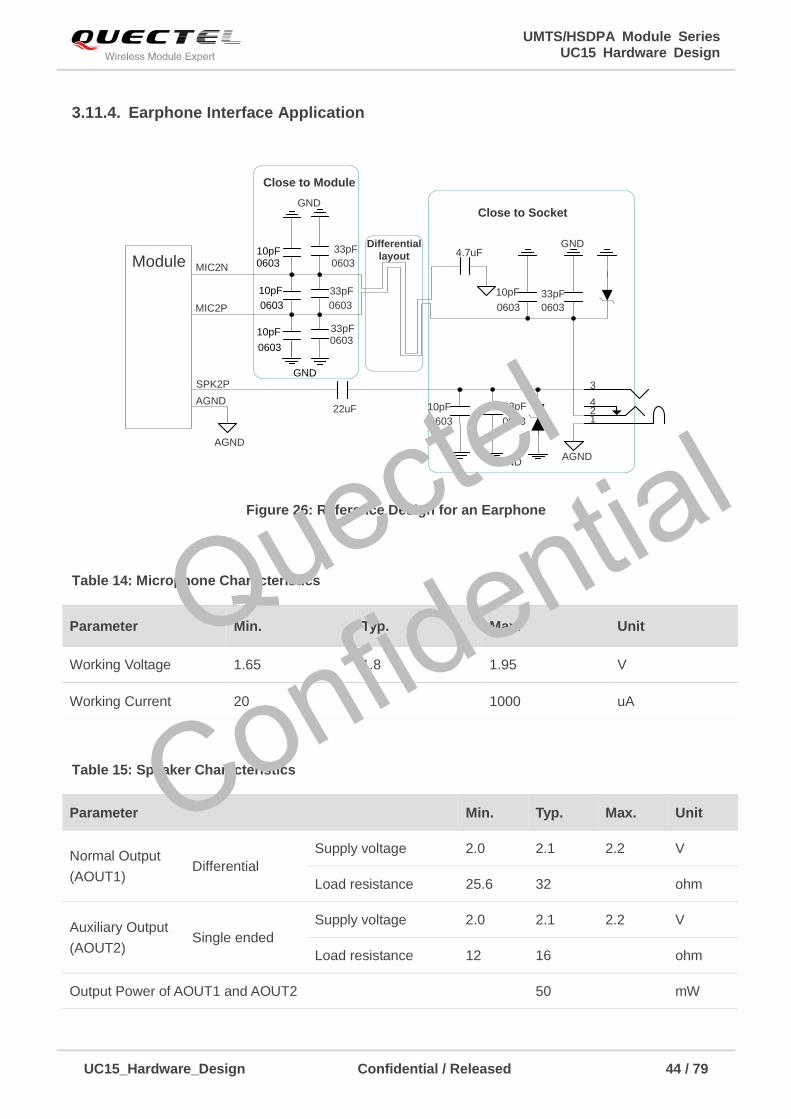
UMTS/HSDPA Module Series UC15 Hardware Design
UC15_Hardware_Design Confidential / Released 44 / 79
3.11.4. Earphone Interface Application
124
3
MIC2P
22uF
33pF
GND
AGND
Close to Socket
AGND
33pF10pF
GND
AGND
Module4.7uF
SPK2P
Close to Module
GND
33pF
33pF
Differential
layout33pF
MIC2N 0603
0603
0603 0603
06030603
0603
10pF
GND
10pF0603
0603
0603
10pF
10pF
Figure 26: Reference Design for an Earphone
Table 14: Microphone Characteristics
Table 15: Speaker Characteristics
Parameter Min. Typ. Max. Unit
Working Voltage 1.65 1.8 1.95 V
Working Current 20 1000 uA
Parameter Min. Typ. Max. Unit
Normal Output
(AOUT1) Differential
Supply voltage 2.0 2.1 2.2 V
Load resistance 25.6 32 ohm
Auxiliary Output
(AOUT2) Single ended
Supply voltage 2.0 2.1 2.2 V
Load resistance 12 16 ohm
Output Power of AOUT1 and AOUT2 50 mW
Quectel
Confidential
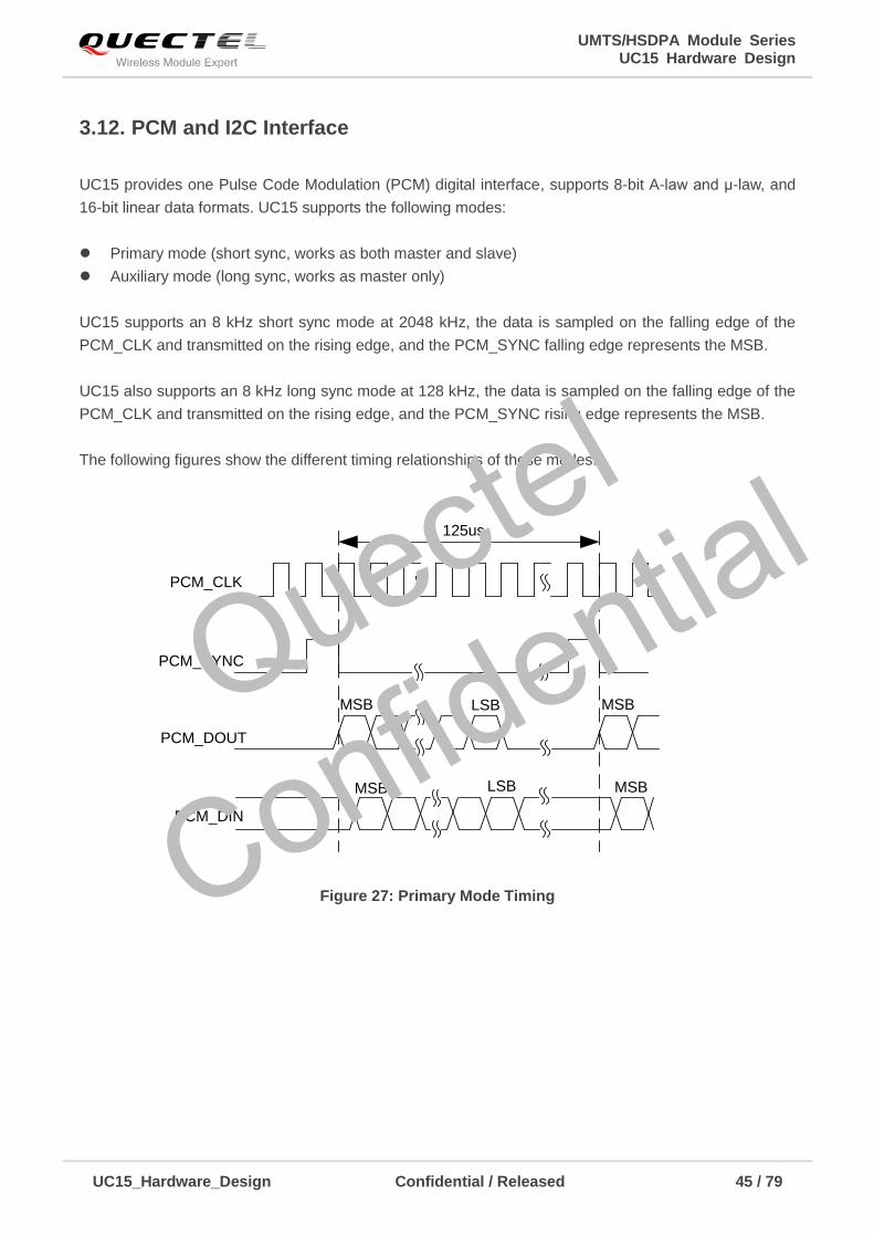
UMTS/HSDPA Module Series UC15 Hardware Design
UC15_Hardware_Design Confidential / Released 45 / 79
3.12. PCM and I2C Interface
UC15 provides one Pulse Code Modulation (PCM) digital interface, supports 8-bit A-law and μ-law, and
16-bit linear data formats. UC15 supports the following modes:
Primary mode (short sync, works as both master and slave)
Auxiliary mode (long sync, works as master only)
UC15 supports an 8 kHz short sync mode at 2048 kHz, the data is sampled on the falling edge of the
PCM_CLK and transmitted on the rising edge, and the PCM_SYNC falling edge represents the MSB.
UC15 also supports an 8 kHz long sync mode at 128 kHz, the data is sampled on the falling edge of the
PCM_CLK and transmitted on the rising edge, and the PCM_SYNC rising edge represents the MSB.
The following figures show the different timing relationships of these modes.
PCM_CLK
PCM_SYNC
PCM_DOUT
MSB LSB MSB
MSB LSB MSB
PCM_DIN
125us
Figure 27: Primary Mode Timing
Quectel
Confidential
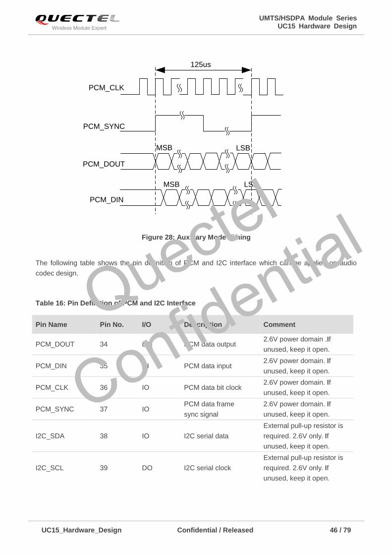
UMTS/HSDPA Module Series UC15 Hardware Design
UC15_Hardware_Design Confidential / Released 46 / 79
PCM_CLK
PCM_SYNC
PCM_DOUT
MSB LSB
PCM_DIN
125us
LSBMSB
Figure 28: Auxiliary Mode Timing
The following table shows the pin definition of PCM and I2C interface which can be applied on audio
codec design.
Table 16: Pin Definition of PCM and I2C Interface
Pin Name Pin No. I/O Description Comment
PCM_DOUT 34 DO PCM data output 2.6V power domain .If
unused, keep it open.
PCM_DIN 35 DI PCM data input 2.6V power domain. If
unused, keep it open.
PCM_CLK 36 IO PCM data bit clock 2.6V power domain. If
unused, keep it open.
PCM_SYNC 37 IO PCM data frame
sync signal
2.6V power domain. If
unused, keep it open.
I2C_SDA 38 IO I2C serial data
External pull-up resistor is
required. 2.6V only. If
unused, keep it open.
I2C_SCL 39 DO I2C serial clock
External pull-up resistor is
required. 2.6V only. If
unused, keep it open.
Quectel
Confidential
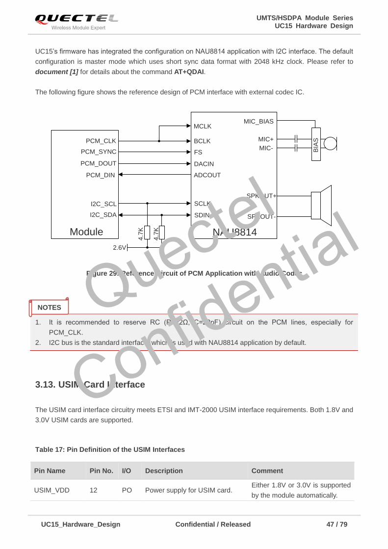
UMTS/HSDPA Module Series UC15 Hardware Design
UC15_Hardware_Design Confidential / Released 47 / 79
UC15’s firmware has integrated the configuration on NAU8814 application with I2C interface. The default
configuration is master mode which uses short sync data format with 2048 kHz clock. Please refer to
document [1] for details about the command AT+QDAI.
The following figure shows the reference design of PCM interface with external codec IC.
PCM_DIN
PCM_DOUT
PCM_SYNC
PCM_CLK
I2C_SCL
I2C_SDA
NAU8814Module
2.6V
4.7
K
4.7
K
BCLK
MCLK
FS
DACIN
ADCOUT
SCLK
SDIN
BIA
S
MIC_BIAS
MIC+
MIC-
SPKOUT+
SPKOUT-
Figure 29: Reference Circuit of PCM Application with Audio Codec
1. It is recommended to reserve RC (R=22Ω, C=22pF) circuit on the PCM lines, especially for
PCM_CLK.
2. I2C bus is the standard interface, which is used with NAU8814 application by default.
3.13. USIM Card Interface
The USIM card interface circuitry meets ETSI and IMT-2000 USIM interface requirements. Both 1.8V and
3.0V USIM cards are supported.
Table 17: Pin Definition of the USIM Interfaces
Pin Name Pin No. I/O Description Comment
USIM_VDD 12 PO Power supply for USIM card. Either 1.8V or 3.0V is supported
by the module automatically.
NOTES Quectel
Confidential
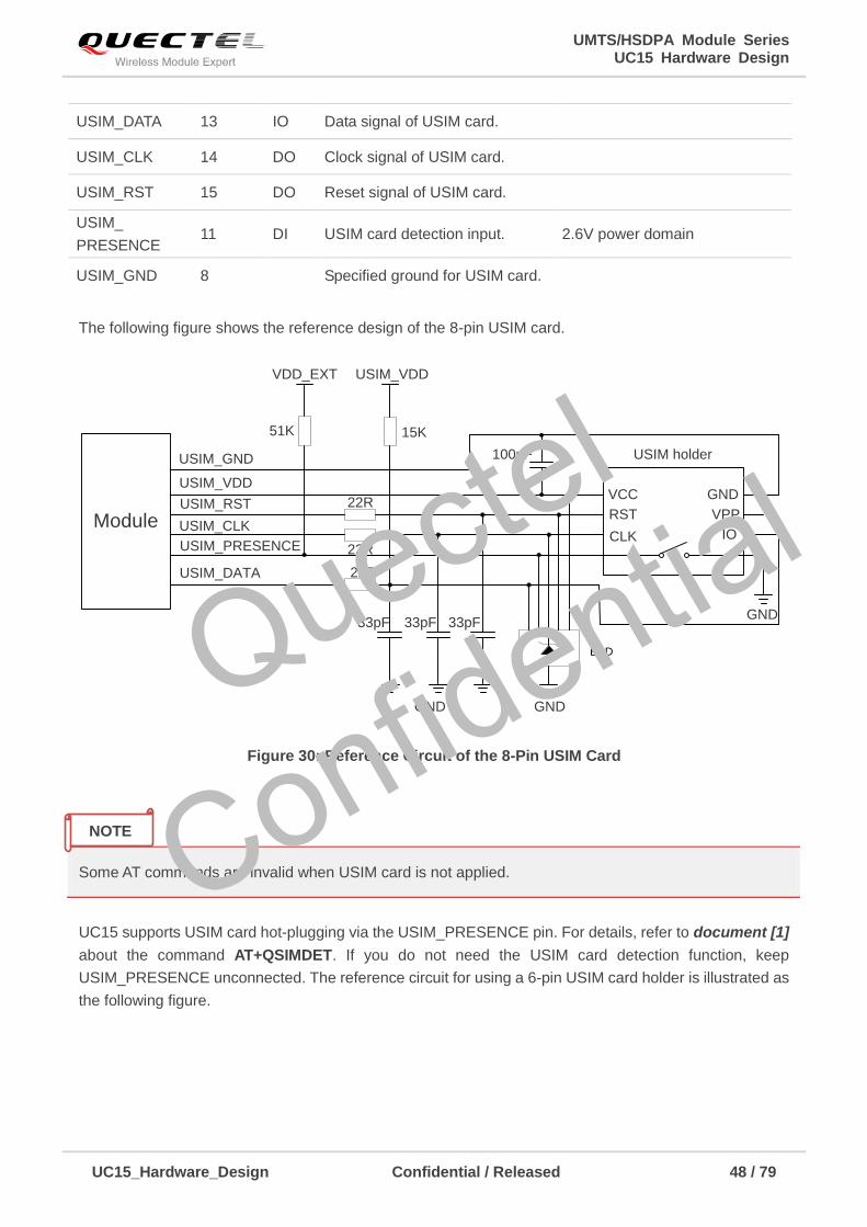
UMTS/HSDPA Module Series UC15 Hardware Design
UC15_Hardware_Design Confidential / Released 48 / 79
The following figure shows the reference design of the 8-pin USIM card.
Module
USIM_VDD
USIM_GND
USIM_RST
USIM_CLK
USIM_DATA
USIM_PRESENCE
22R
22R
22R
VDD_EXT
51K
100nF USIM holder
GND
GND33pF 33pF 33pF
VCC
RST
CLK IO
VPP
GND
GND
USIM_VDD
15K
ESD
Figure 30: Reference Circuit of the 8-Pin USIM Card
Some AT commands are invalid when USIM card is not applied.
UC15 supports USIM card hot-plugging via the USIM_PRESENCE pin. For details, refer to document [1]
about the command AT+QSIMDET. If you do not need the USIM card detection function, keep
USIM_PRESENCE unconnected. The reference circuit for using a 6-pin USIM card holder is illustrated as
the following figure.
USIM_DATA 13 IO Data signal of USIM card.
USIM_CLK 14 DO Clock signal of USIM card.
USIM_RST 15 DO Reset signal of USIM card.
USIM_
PRESENCE 11 DI USIM card detection input. 2.6V power domain
USIM_GND 8 Specified ground for USIM card.
NOTE
Quectel
Confidential
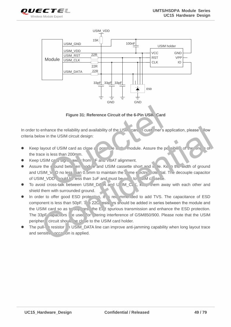
UMTS/HSDPA Module Series UC15 Hardware Design
UC15_Hardware_Design Confidential / Released 49 / 79
Module
USIM_VDD
USIM_GND
USIM_RST
USIM_CLK
USIM_DATA 22R
22R
22R
100nFUSIM holder
GND
33pF 33pF 33pF
VCC
RST
CLK IO
VPP
GND
GND
15K
USIM_VDD
ESD
Figure 31: Reference Circuit of the 6-Pin USIM Card
In order to enhance the reliability and availability of the USIM card in customer’s application, please follow
criteria below in the USIM circuit design:
Keep layout of USIM card as close as possible to the module. Assure the possibility of the length of
the trace is less than 200mm.
Keep USIM card signal away from RF and VBAT alignment.
Assure the ground between module and USIM cassette short and wide. Keep the width of ground
and USIM_VDD no less than 0.5mm to maintain the same electric potential. The decouple capacitor
of USIM_VDD should be less than 1uF and must be near to USIM cassette.
To avoid cross-talk between USIM_DATA and USIM_CLK, keep them away with each other and
shield them with surrounded ground.
In order to offer good ESD protection, it is recommended to add TVS. The capacitance of ESD
component is less than 50pF. The 22Ω resistors should be added in series between the module and
the USIM card so as to suppress the EMI spurious transmission and enhance the ESD protection.
The 33pF capacitors are used for filtering interference of GSM850/900. Please note that the USIM
peripheral circuit should be close to the USIM card holder.
The pull-up resistor on USIM_DATA line can improve anti-jamming capability when long layout trace
and sensitive occasion is applied.
Quectel
Confidential
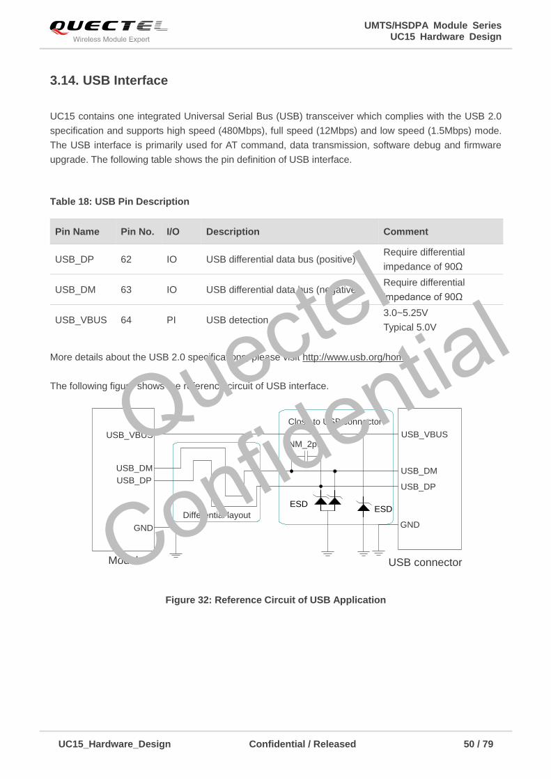
UMTS/HSDPA Module Series UC15 Hardware Design
UC15_Hardware_Design Confidential / Released 50 / 79
3.14. USB Interface
UC15 contains one integrated Universal Serial Bus (USB) transceiver which complies with the USB 2.0
specification and supports high speed (480Mbps), full speed (12Mbps) and low speed (1.5Mbps) mode.
The USB interface is primarily used for AT command, data transmission, software debug and firmware
upgrade. The following table shows the pin definition of USB interface.
Table 18: USB Pin Description
More details about the USB 2.0 specifications, please visit http://www.usb.org/home.
The following figure shows the reference circuit of USB interface.
Module
USB_VBUS
USB_DP
USB_DM
GND
USB connector
Close to USB connector
Differential layout
USB_VBUS
USB_DP
USB_DM
GND
NM_2pF
ESDESD
Figure 32: Reference Circuit of USB Application
Pin Name Pin No. I/O Description Comment
USB_DP 62 IO USB differential data bus (positive) Require differential
impedance of 90Ω
USB_DM 63 IO USB differential data bus (negative) Require differential
impedance of 90Ω
USB_VBUS 64 PI USB detection 3.0~5.25V
Typical 5.0V
Quectel
Confidential
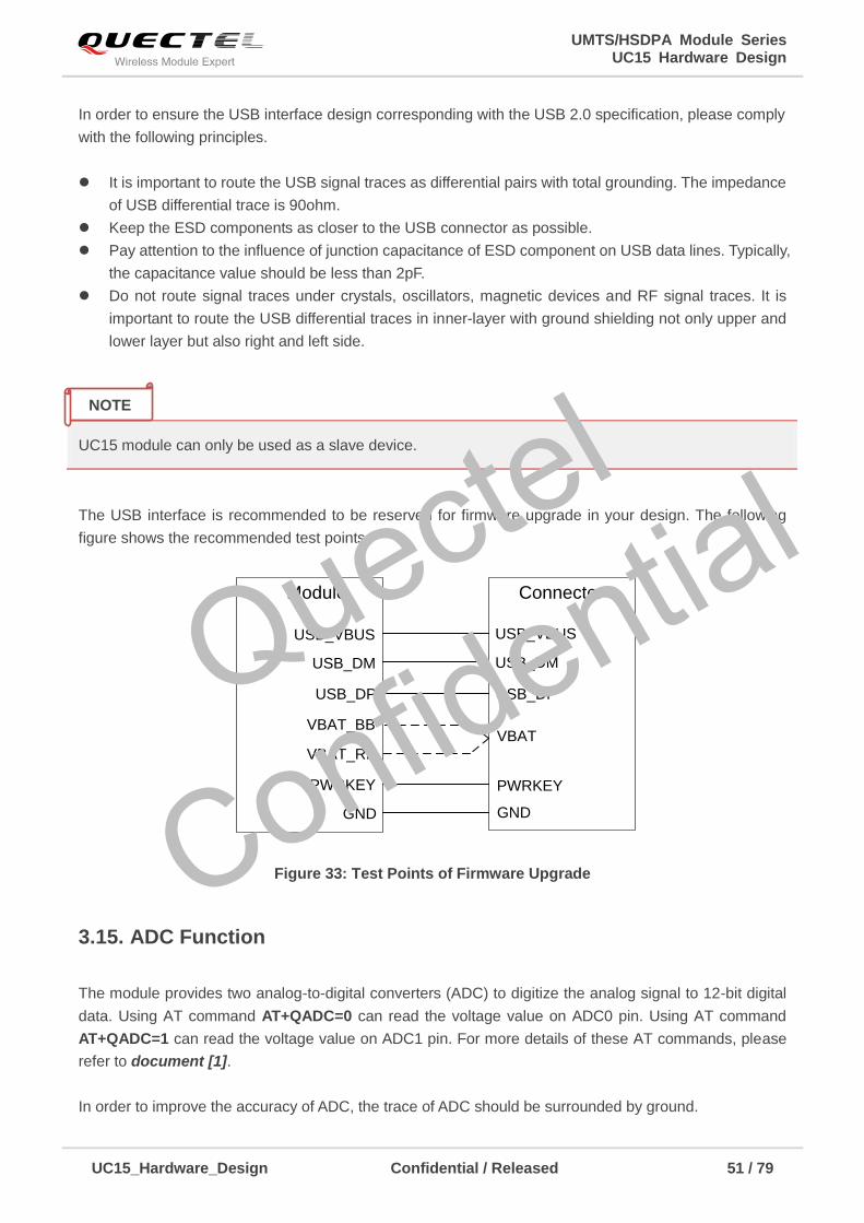
UMTS/HSDPA Module Series UC15 Hardware Design
UC15_Hardware_Design Confidential / Released 51 / 79
In order to ensure the USB interface design corresponding with the USB 2.0 specification, please comply
with the following principles.
It is important to route the USB signal traces as differential pairs with total grounding. The impedance
of USB differential trace is 90ohm.
Keep the ESD components as closer to the USB connector as possible.
Pay attention to the influence of junction capacitance of ESD component on USB data lines. Typically,
the capacitance value should be less than 2pF.
Do not route signal traces under crystals, oscillators, magnetic devices and RF signal traces. It is
important to route the USB differential traces in inner-layer with ground shielding not only upper and
lower layer but also right and left side.
UC15 module can only be used as a slave device.
The USB interface is recommended to be reserved for firmware upgrade in your design. The following
figure shows the recommended test points.
Module
USB_DM
USB_DP
VBAT_BB
USB_VBUS
PWRKEY
GND
VBAT_RF
USB_DM
USB_DP
VBAT
USB_VBUS
PWRKEY
GND
Connector
Figure 33: Test Points of Firmware Upgrade
3.15. ADC Function
The module provides two analog-to-digital converters (ADC) to digitize the analog signal to 12-bit digital
data. Using AT command AT+QADC=0 can read the voltage value on ADC0 pin. Using AT command
AT+QADC=1 can read the voltage value on ADC1 pin. For more details of these AT commands, please
refer to document [1].
In order to improve the accuracy of ADC, the trace of ADC should be surrounded by ground.
NOTE
Quectel
Confidential
UMTS/HSDPA Module Series UC15 Hardware Design
UC15_Hardware_Design Confidential / Released 52 / 79
Table 19: Pin Definition of the ADC
The following table describes the characteristics of the ADC function.
Table 20: Characteristics of the ADC
3.16. Network Status Indication
The module provides a pin named NETLIGHT to indicate the module network status which can be used to
drive a LED. The following tables describe pin definition and logic level changes in different network
status.
Table 21: Pin Definition of Network Indicator
Table 22: Working State of the Network Indicator
Pin Name Pin NO. Description
ADC0 41 General purpose analog to digital converter.
ADC1 40 General purpose analog to digital converter.
Parameter Min. Typ. Max. Unit
ADC0 Voltage Range 0 2.1 V
ADC1 Voltage Range 0 2.1 V
Sample Rate 2.4 MHz
ADC Resolution 12 bits
Pin Name Pin No. I/O Description Comment
NETLIGHT 6 DO Indicate the module network activity
status.
2.6V power domain. If
unused, keep it open.
Pin Name Status Description
NETLIGHT
200ms High/1800ms Low Network searching
1800ms High/200ms Low Idle
Quectel
Confidential
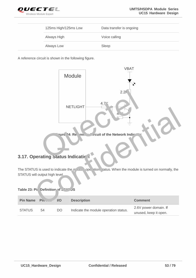
UMTS/HSDPA Module Series UC15 Hardware Design
UC15_Hardware_Design Confidential / Released 53 / 79
A reference circuit is shown in the following figure.
4.7K
47K
VBAT
2.2K
Module
NETLIGHT
Figure 34: Reference Circuit of the Network Indicator
3.17. Operating Status Indication
The STATUS is used to indicate the module operation status. When the module is turned on normally, the
STATUS will output high level.
Table 23: Pin Definition of STATUS
125ms High/125ms Low Data transfer is ongoing
Always High Voice calling
Always Low Sleep
Pin Name Pin No. I/O Description Comment
STATUS 54 DO Indicate the module operation status. 2.6V power domain. If
unused, keep it open.
Quectel
Confidential
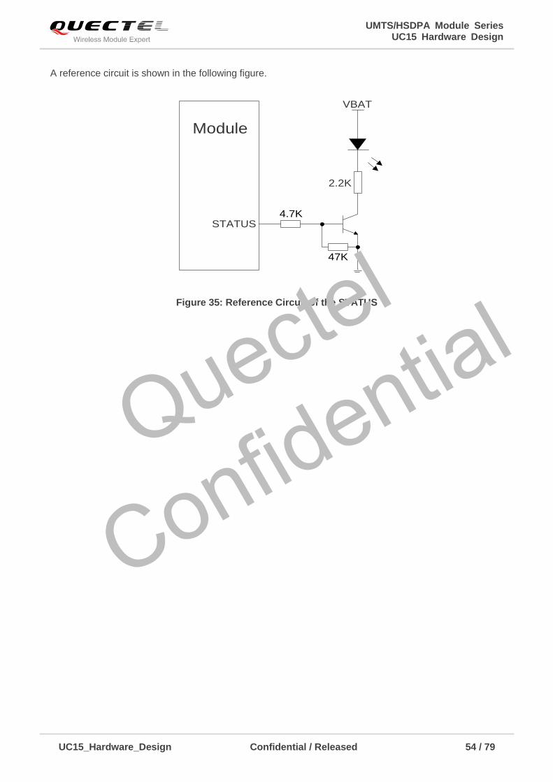
UMTS/HSDPA Module Series UC15 Hardware Design
UC15_Hardware_Design Confidential / Released 54 / 79
A reference circuit is shown in the following figure.
Module
STATUS
VBAT
2.2K
4.7K
47K
Figure 35: Reference Circuit of the STATUS
Quectel
Confidential
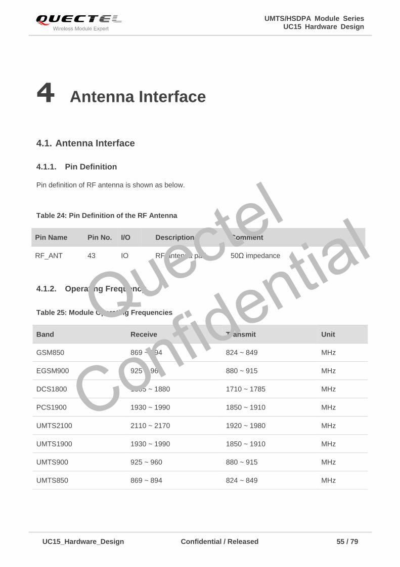
UMTS/HSDPA Module Series UC15 Hardware Design
UC15_Hardware_Design Confidential / Released 55 / 79
4 Antenna Interface
4.1. Antenna Interface
4.1.1. Pin Definition
Pin definition of RF antenna is shown as below.
Table 24: Pin Definition of the RF Antenna
4.1.2. Operating Frequency
Table 25: Module Operating Frequencies
Pin Name Pin No. I/O Description Comment
RF_ANT 43 IO RF antenna pad 50Ω impedance
Band Receive Transmit Unit
GSM850 869 ~ 894 824 ~ 849 MHz
EGSM900 925 ~ 960 880 ~ 915 MHz
DCS1800 1805 ~ 1880 1710 ~ 1785 MHz
PCS1900 1930 ~ 1990 1850 ~ 1910 MHz
UMTS2100 2110 ~ 2170 1920 ~ 1980 MHz
UMTS1900 1930 ~ 1990 1850 ~ 1910 MHz
UMTS900 925 ~ 960 880 ~ 915 MHz
UMTS850 869 ~ 894 824 ~ 849 MHz
Quectel
Confidential
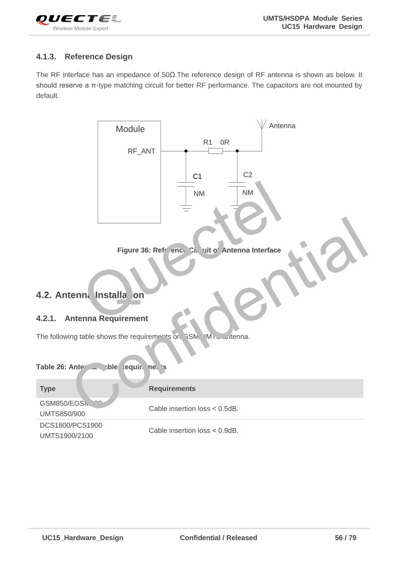
UMTS/HSDPA Module Series UC15 Hardware Design
UC15_Hardware_Design Confidential / Released 56 / 79
4.1.3. Reference Design
The RF interface has an impedance of 50Ω.The reference design of RF antenna is shown as below. It
should reserve a π-type matching circuit for better RF performance. The capacitors are not mounted by
default.
RF_ANT
R1 0R
C1
Module Antenna
NM
C2
NM
Figure 36: Reference Circuit of Antenna Interface
4.2. Antenna Installation
4.2.1. Antenna Requirement
The following table shows the requirements on GSM/UMTS antenna.
Table 26: Antenna Cable Requirements
Type Requirements
GSM850/EGSM900
UMTS850/900 Cable insertion loss < 0.5dB.
DCS1800/PCS1900
UMTS1900/2100 Cable insertion loss < 0.9dB.
Quectel
Confidential
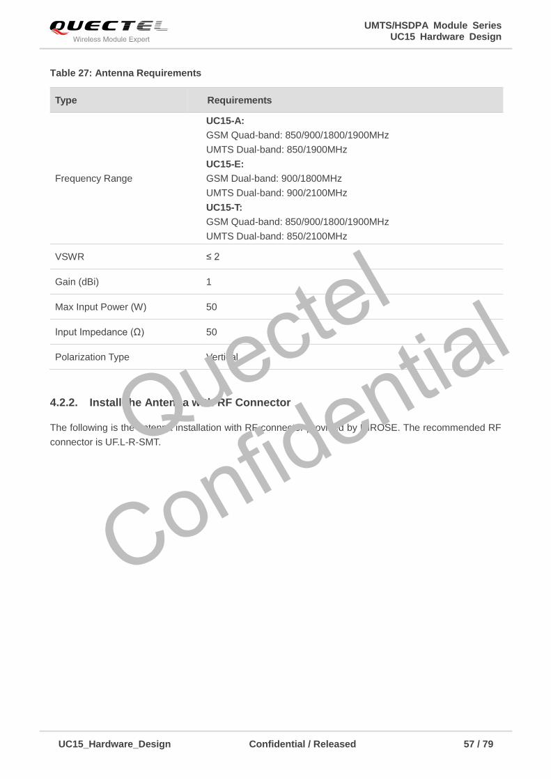
UMTS/HSDPA Module Series UC15 Hardware Design
UC15_Hardware_Design Confidential / Released 57 / 79
Table 27: Antenna Requirements
Type Requirements
Frequency Range
UC15-A:
GSM Quad-band: 850/900/1800/1900MHz
UMTS Dual-band: 850/1900MHz
UC15-E:
GSM Dual-band: 900/1800MHz
UMTS Dual-band: 900/2100MHz
UC15-T:
GSM Quad-band: 850/900/1800/1900MHz
UMTS Dual-band: 850/2100MHz
VSWR ≤ 2
Gain (dBi) 1
Max Input Power (W) 50
Input Impedance (Ω) 50
Polarization Type Vertical
4.2.2. Install the Antenna with RF Connector
The following is the antenna installation with RF connector provided by HIROSE. The recommended RF
connector is UF.L-R-SMT. Quectel
Confidential
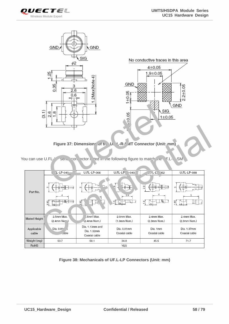
UMTS/HSDPA Module Series UC15 Hardware Design
UC15_Hardware_Design Confidential / Released 58 / 79
Figure 37: Dimensions of the UF.L-R-SMT Connector (Unit: mm)
You can use U.FL-LP serial connector listed in the following figure to match the UF.L-R-SMT.
Figure 38: Mechanicals of UF.L-LP Connectors (Unit: mm)
Quectel
Confidential
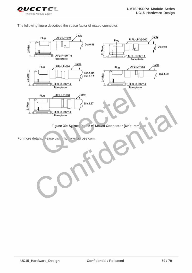
UMTS/HSDPA Module Series UC15 Hardware Design
UC15_Hardware_Design Confidential / Released 59 / 79
The following figure describes the space factor of mated connector:
Figure 39: Space Factor of Mated Connector (Unit: mm)
For more details, please visit http://www.hirose.com. Quectel
Confidential
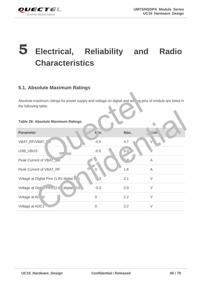
UMTS/HSDPA Module Series UC15 Hardware Design
UC15_Hardware_Design Confidential / Released 60 / 79
5 Electrical, Reliability and Radio
Characteristics
5.1. Absolute Maximum Ratings
Absolute maximum ratings for power supply and voltage on digital and analog pins of module are listed in
the following table:
Table 28: Absolute Maximum Ratings
Parameter Min. Max. Unit
VBAT_RF/VBAT_BB -0.5 4.7 V
USB_VBUS -0.5 6.0 V
Peak Current of VBAT_BB 0 0.8 A
Peak Current of VBAT_RF 0 1.8 A
Voltage at Digital Pins (1.8V digital I/O) -0.3 2.1 V
Voltage at Digital Pins (2.6V digital I/O) -0.3 2.9 V
Voltage at ADC0 0 2.2 V
Voltage at ADC1 0 2.2 V
Quectel
Confidential
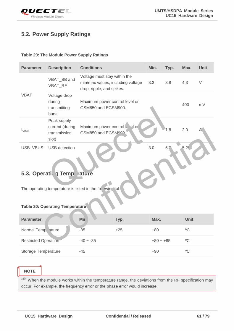
UMTS/HSDPA Module Series UC15 Hardware Design
UC15_Hardware_Design Confidential / Released 61 / 79
5.2. Power Supply Ratings
Table 29: The Module Power Supply Ratings
5.3. Operating Temperature
The operating temperature is listed in the following table.
Table 30: Operating Temperature
“1)
” When the module works within the temperature range, the deviations from the RF specification may
occur. For example, the frequency error or the phase error would increase.
Parameter Description Conditions Min. Typ. Max. Unit
VBAT
VBAT_BB and
VBAT_RF
Voltage must stay within the
min/max values, including voltage
drop, ripple, and spikes.
3.3 3.8 4.3 V
Voltage drop
during
transmitting
burst
Maximum power control level on
GSM850 and EGSM900. 400 mV
IVBAT
Peak supply
current (during
transmission
slot)
Maximum power control level on
GSM850 and EGSM900. 1.8 2.0 A
USB_VBUS USB detection 3.0 5.0 5.25 V
Parameter Min. Typ. Max. Unit
Normal Temperature -35 +25 +80 ºC
Restricted Operation1)
-40 ~ -35 +80 ~ +85 ºC
Storage Temperature -45 +90 ºC
NOTE
Quectel
Confidential
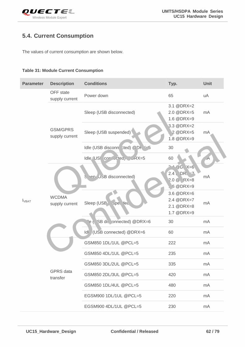
UMTS/HSDPA Module Series UC15 Hardware Design
UC15_Hardware_Design Confidential / Released 62 / 79
5.4. Current Consumption
The values of current consumption are shown below.
Table 31: Module Current Consumption
Parameter Description Conditions Typ. Unit
IVBAT
OFF state
supply current Power down 65 uA
GSM/GPRS
supply current
Sleep (USB disconnected)
3.1 @DRX=2
2.0 @DRX=5
1.6 @DRX=9
mA
Sleep (USB suspended)
3.3 @DRX=2
2.2 @DRX=5
1.8 @DRX=9
mA
Idle (USB disconnected) @DRX=5 30 mA
Idle (USB connected) @DRX=5 60 mA
WCDMA
supply current
Sleep (USB disconnected)
3.4 @DRX=6
2.4 @DRX=7
2.0 @DRX=8
1.6 @DRX=9
mA
Sleep (USB suspended)
3.6 @DRX=6
2.4 @DRX=7
2.1 @DRX=8
1.7 @DRX=9
mA
Idle (USB disconnected) @DRX=6 30 mA
Idle (USB connected) @DRX=6 60 mA
GPRS data
transfer
GSM850 1DL/1UL @PCL=5 222 mA
GSM850 4DL/1UL @PCL=5 235 mA
GSM850 3DL/2UL @PCL=5 335 mA
GSM850 2DL/3UL @PCL=5 420 mA
GSM850 1DL/4UL @PCL=5 480 mA
EGSM900 1DL/1UL @PCL=5 220 mA
EGSM900 4DL/1UL @PCL=5 230 mA
Quectel
Confidential
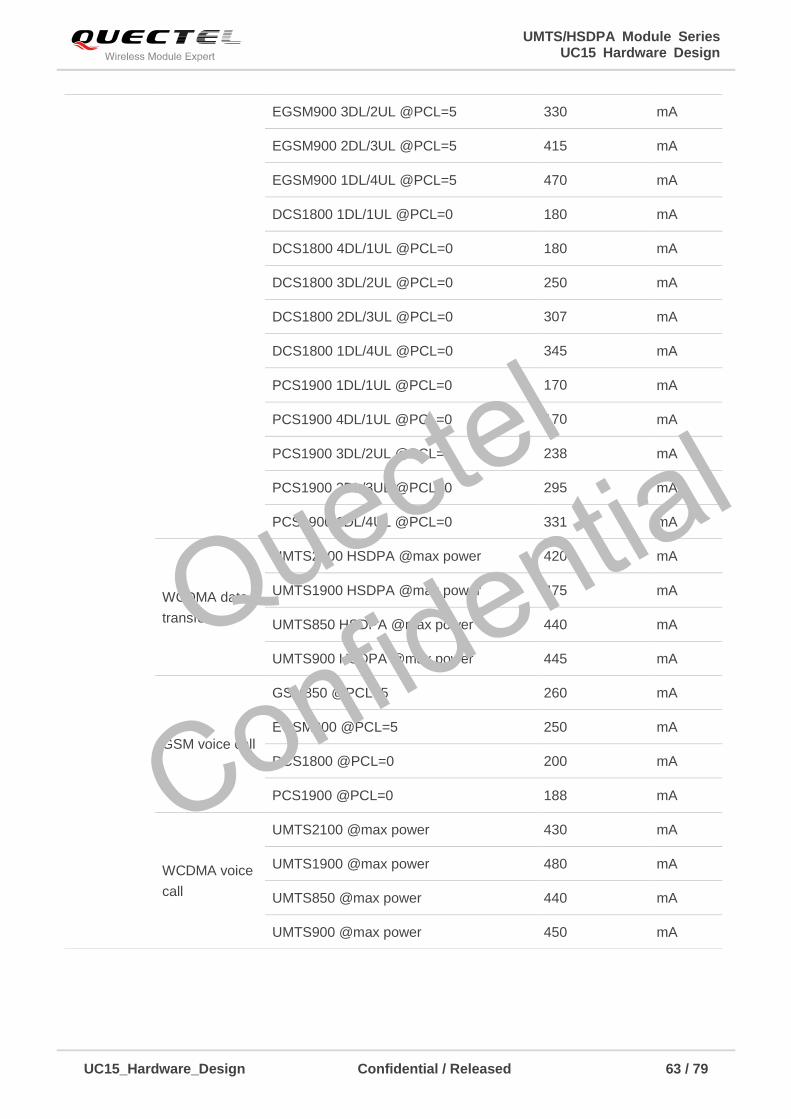
UMTS/HSDPA Module Series UC15 Hardware Design
UC15_Hardware_Design Confidential / Released 63 / 79
EGSM900 3DL/2UL @PCL=5 330 mA
EGSM900 2DL/3UL @PCL=5 415 mA
EGSM900 1DL/4UL @PCL=5 470 mA
DCS1800 1DL/1UL @PCL=0 180 mA
DCS1800 4DL/1UL @PCL=0 180 mA
DCS1800 3DL/2UL @PCL=0 250 mA
DCS1800 2DL/3UL @PCL=0 307 mA
DCS1800 1DL/4UL @PCL=0 345 mA
PCS1900 1DL/1UL @PCL=0 170 mA
PCS1900 4DL/1UL @PCL=0 170 mA
PCS1900 3DL/2UL @PCL=0 238 mA
PCS1900 2DL/3UL @PCL=0 295 mA
PCS1900 1DL/4UL @PCL=0 331 mA
WCDMA data
transfer
UMTS2100 HSDPA @max power 420 mA
UMTS1900 HSDPA @max power 475 mA
UMTS850 HSDPA @max power 440 mA
UMTS900 HSDPA @max power 445 mA
GSM voice call
GSM850 @PCL=5 260 mA
EGSM900 @PCL=5 250 mA
DCS1800 @PCL=0 200 mA
PCS1900 @PCL=0 188 mA
WCDMA voice
call
UMTS2100 @max power 430 mA
UMTS1900 @max power 480 mA
UMTS850 @max power 440 mA
UMTS900 @max power 450 mA
Quectel
Confidential
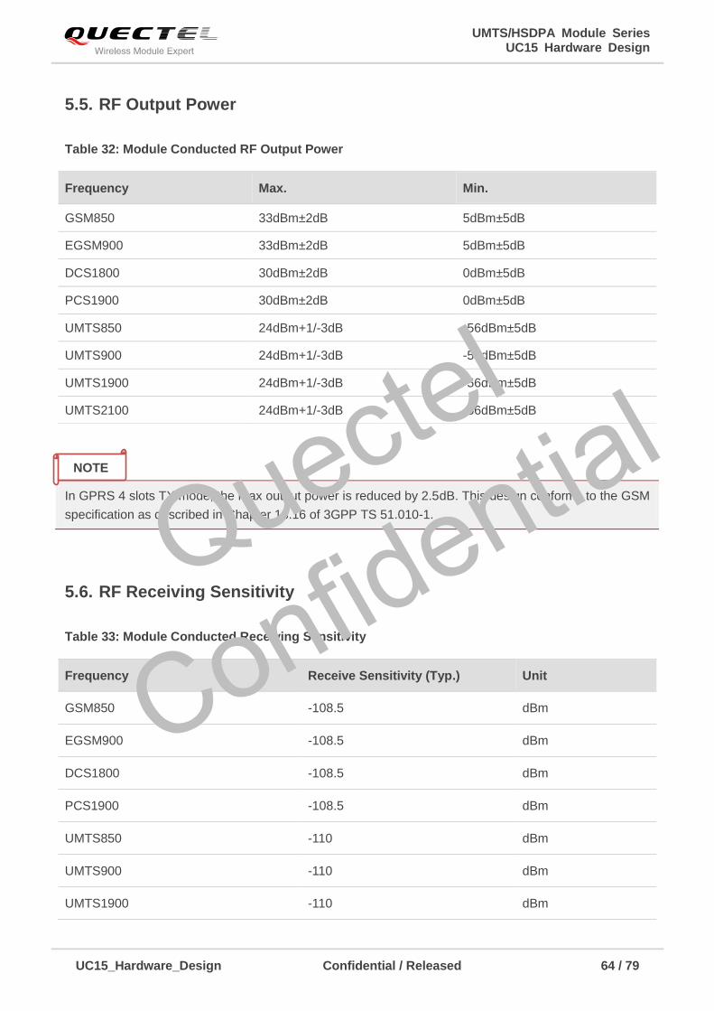
UMTS/HSDPA Module Series UC15 Hardware Design
UC15_Hardware_Design Confidential / Released 64 / 79
5.5. RF Output Power
Table 32: Module Conducted RF Output Power
In GPRS 4 slots TX mode, the max output power is reduced by 2.5dB. This design conforms to the GSM
specification as described in Chapter 13.16 of 3GPP TS 51.010-1.
5.6. RF Receiving Sensitivity
Table 33: Module Conducted Receiving Sensitivity
Frequency Max. Min.
GSM850 33dBm±2dB 5dBm±5dB
EGSM900 33dBm±2dB 5dBm±5dB
DCS1800 30dBm±2dB 0dBm±5dB
PCS1900 30dBm±2dB 0dBm±5dB
UMTS850 24dBm+1/-3dB -56dBm±5dB
UMTS900 24dBm+1/-3dB -56dBm±5dB
UMTS1900 24dBm+1/-3dB -56dBm±5dB
UMTS2100 24dBm+1/-3dB -56dBm±5dB
Frequency Receive Sensitivity (Typ.) Unit
GSM850 -108.5 dBm
EGSM900 -108.5 dBm
DCS1800 -108.5 dBm
PCS1900 -108.5 dBm
UMTS850 -110 dBm
UMTS900 -110 dBm
UMTS1900 -110 dBm
NOTE
Quectel
Confidential
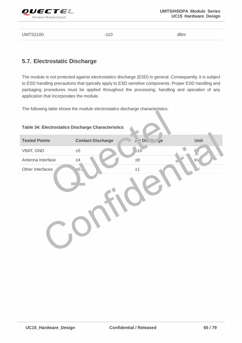
UMTS/HSDPA Module Series UC15 Hardware Design
UC15_Hardware_Design Confidential / Released 65 / 79
5.7. Electrostatic Discharge
The module is not protected against electrostatics discharge (ESD) in general. Consequently, it is subject
to ESD handling precautions that typically apply to ESD sensitive components. Proper ESD handling and
packaging procedures must be applied throughout the processing, handling and operation of any
application that incorporates the module.
The following table shows the module electrostatics discharge characteristics.
Table 34: Electrostatics Discharge Characteristics
UMTS2100 -110 dBm
Tested Points Contact Discharge Air Discharge Unit
VBAT, GND ±5 ±10 kV
Antenna Interface ±4 ±8 kV
Other Interfaces ±0.5 ±1 kV
Quectel
Confidential
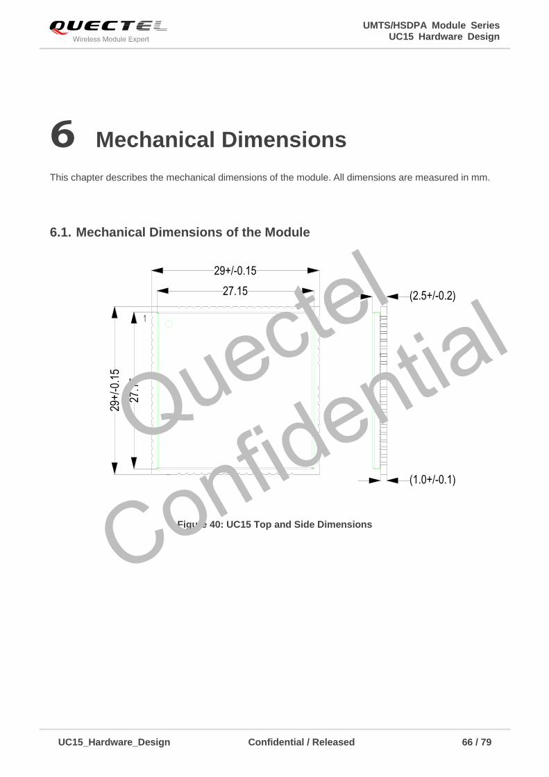
UMTS/HSDPA Module Series UC15 Hardware Design
UC15_Hardware_Design Confidential / Released 66 / 79
6 Mechanical Dimensions
This chapter describes the mechanical dimensions of the module. All dimensions are measured in mm.
6.1. Mechanical Dimensions of the Module
(2.5+/-0.2)
(1.0+/-0.1)
27.1
5
27.15
29+
/-0.
15
29+/-0.15
Figure 40: UC15 Top and Side Dimensions
Quectel
Confidential
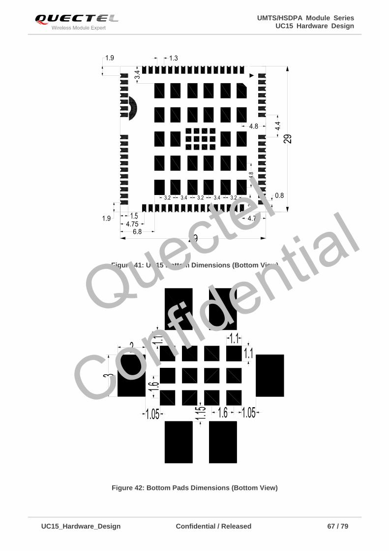
UMTS/HSDPA Module Series UC15 Hardware Design
UC15_Hardware_Design Confidential / Released 67 / 79
29
29
4.8
3.23.43.23.43.2
3.4
Figure 41: UC15 Bottom Dimensions (Bottom View)
Figure 42: Bottom Pads Dimensions (Bottom View)
Quectel
Confidential
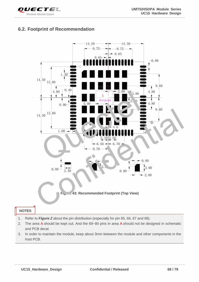
UMTS/HSDPA Module Series UC15 Hardware Design
UC15_Hardware_Design Confidential / Released 68 / 79
6.2. Footprint of Recommendation
0.80 2.50
2.00
3.000.80
0.80
3.00
2.00
0.404.80
12.60
0.90
12.60
14.50 14.50
14.50
14.50
3.10
6.50
3.50
6.70
0.10
4.80
9.60
4.80
9.60
0.65
9.75
0.65
9.75
0.80
1.30
9.70
1.00
A
2.80
2.00
5.00
2.80
keepout
Figure 43: Recommended Footprint (Top View)
1. Refer to Figure 2 about the pin distribution (especially for pin 65, 66, 67 and 68).
2. The area A should be kept out. And the 69~80 pins in area A should not be designed in schematic
and PCB decal.
3. In order to maintain the module, keep about 3mm between the module and other components in the
host PCB.
NOTES
Quectel
Confidential
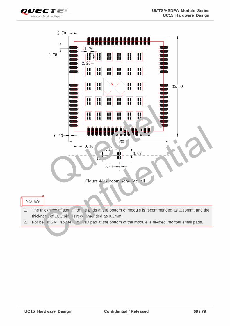
UMTS/HSDPA Module Series UC15 Hardware Design
UC15_Hardware_Design Confidential / Released 69 / 79
32.60
32.60
2.70
0.75
1.20
2.20
A
0.30
0.50
0.97
0.47
0.13
0.13
Figure 44: Recommend Stencil
1. The thickness of stencil for the pads at the bottom of module is recommended as 0.18mm, and the
thickness of LCC pins is recommended as 0.2mm.
2. For better SMT solder, the GND pad at the bottom of the module is divided into four small pads.
NOTES
Quectel
Confidential
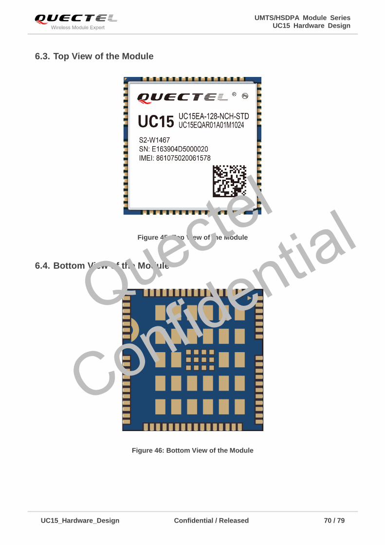
UMTS/HSDPA Module Series UC15 Hardware Design
UC15_Hardware_Design Confidential / Released 70 / 79
6.3. Top View of the Module
Figure 45: Top View of the Module
6.4. Bottom View of the Module
Figure 46: Bottom View of the Module
Quectel
Confidential
UMTS/HSDPA Module Series UC15 Hardware Design
UC15_Hardware_Design Confidential / Released 71 / 79
7 Storage and Manufacturing
7.1. Storage
UC15 is stored in the vacuum-sealed bag. The restriction of storage condition is shown as below.
Shelf life in sealed bag is 12 months at < 40ºC/90%RH.
After this bag is opened, devices that will be subjected to reflow solder or other high temperature process
must be:
Mounted within 72 hours at factory conditions of ≤ 30ºC/60%RH.
Stored at < 10% RH.
Devices require bake, before mounting, if:
Humidity indicator card is > 10% when read 23ºC±5ºC.
Mounted for more than 72 hours at factory conditions of ≤ 30ºC/60% RH.
If baking is required, devices may be baked for 48 hours at 125ºC±5ºC.
As plastic container cannot be subjected to high temperature, module needs to be taken out from
container to high temperature (125ºC) bake. If shorter bake times are desired, please refer to
IPC/JEDECJ-STD-033 for bake procedure.
7.2. Manufacturing and Welding
The squeegee should push the paste on the surface of the stencil that makes the paste fill the stencil
openings and penetrate to the PCB. The force on the squeegee should be adjusted so as to produce a
clean stencil surface on a single pass. To ensure the module soldering quality, the thickness of stencil at
the hole of the module pads should be 0.18mm. For details, please refer to document [4].
NOTE
Quectel
Confidential
UMTS/HSDPA Module Series UC15 Hardware Design
UC15_Hardware_Design Confidential / Released 72 / 79
It is suggested that peak reflow temperature is 235~245ºC (for SnAg3.0Cu0.5 alloy). Absolute max reflow
temperature is 260ºC. To avoid damage to the module when it was repeatedly heated, it is suggested that
the module should be mounted after the first panel has been reflowed. The following picture is the actual
diagram which we have operated.
Time
50 100 150 200 250 300
50
100
150
200
250
160 ºC
200 ºC
217
0
70s~120s
40s~60s
Between 1~3 ºC/s
Preheat Heating CoolingºC
s
Liquids Temperature
Figure 47: Reflow Soldering Profile
Quectel
Confidential
UMTS/HSDPA Module Series UC15 Hardware Design
UC15_Hardware_Design Confidential / Released 73 / 79
7.3. Packaging
UC15 is packaged in the tap and reel carriers. One reel is 12.4m length and contains 250pcs modules.
The following figure shows the package details.
Unit: mm
Direction of feed
Cover tape
Figure 48: Carrier Tape
Quectel
Confidential
UMTS/HSDPA Module Series UC15 Hardware Design
UC15_Hardware_Design Confidential / Released 74 / 79
8 Appendix A Reference
Table 35: Related Documents
Table 36: Terms and Abbreviations
SN Document Name Remark
[1] Quectel_UC15_AT_Commands_Manual UC15 AT commands manual
[2] Quectel_M10_EVB_User_Guide M10 EVB user guide
[3] Quectel_UC15_Reference_Design UC15 reference design
[4] Quectel_Module_Secondary_SMT_User_Guide Module secondary SMT user guide
Abbreviation Description
AMR Adaptive Multi-rate
bps Bits Per Second
CHAP Challenge Handshake Authentication Protocol
CS Coding Scheme
CSD Circuit Switched Data
CTS Clear to Send
DRX Discontinuous Reception
DCE Data Communications Equipment (typical module)
DTE Data Terminal Equipment (typical computer, external controller)
DTR Data Terminal Ready
DTX Discontinuous Transmission
Quectel
Confidential
UMTS/HSDPA Module Series UC15 Hardware Design
UC15_Hardware_Design Confidential / Released 75 / 79
EFR Enhanced Full Rate
EGSM Extended GSM900 Band (including standard GSM900 band)
ESD Electrostatic Discharge
FR Full Rate
GMSK Gaussian Minimum Shift Keying
GSM Global System for Mobile Communications
HR Half Rate
HSDPA High Speed Down Link Packet Access
IMEI International Mobile Equipment Identity
Imax Maximum Load Current
LED Light Emitting Diode
LSB Least Significant Bit
ME Mobile Equipment
MO Mobile Originated
MS Mobile Station (GSM Engine)
MT Mobile Terminated
PAP Password Authentication Protocol
PBCCH Packet Broadcast Control Channel
PCB Printed Circuit Board
PDU Protocol Data Unit
PPP Point-to-Point Protocol
PSK Phase Shift Keying
QAM Quadrature Amplitude Modulation
QPSK Quadrature Phase Shift Keying
RF Radio Frequency
Quectel
Confidential
UMTS/HSDPA Module Series UC15 Hardware Design
UC15_Hardware_Design Confidential / Released 76 / 79
RMS Root Mean Square (value)
Rx Receive
SIM Subscriber Identification Module
SMS Short Message Service
TX Transmitting Direction
UART Universal Asynchronous Receiver & Transmitter
UMTS Universal Mobile Telecommunications System
URC Unsolicited Result Code
USIM Universal Subscriber Identity Module
USSD Unstructured Supplementary Service Data
Vmax Maximum Voltage Value
Vnorm Normal Voltage Value
Vmin Minimum Voltage Value
VIHmax Maximum Input High Level Voltage Value
VIHmin Minimum Input High Level Voltage Value
VILmax Maximum Input Low Level Voltage Value
VILmin Minimum Input Low Level Voltage Value
VImax Absolute Maximum Input Voltage Value
VImin Absolute Minimum Input Voltage Value
VOHmax Maximum Output High Level Voltage Value
VOHmin Minimum Output High Level Voltage Value
VOLmax Maximum Output Low Level Voltage Value
VOLmin Minimum Output Low Level Voltage Value
VSWR Voltage Standing Wave Ratio
WCDMA Wideband Code Division Multiple Access
Quectel
Confidential
UMTS/HSDPA Module Series UC15 Hardware Design
UC15_Hardware_Design Confidential / Released 77 / 79
9 Appendix B GPRS Coding Scheme
Table 37: Description of Different Coding Schemes
Scheme CS-1 CS-2 CS-3 CS-4
Code Rate 1/2 2/3 3/4 1
USF 3 3 3 3
Pre-coded USF 3 6 6 12
Radio Block excl.USF and BCS 181 268 312 428
BCS 40 16 16 16
Tail 4 4 4 -
Coded Bits 456 588 676 456
Punctured Bits 0 132 220 -
Data Rate Kb/s 9.05 13.4 15.6 21.4 Quectel
Confidential
UMTS/HSDPA Module Series UC15 Hardware Design
UC15_Hardware_Design Confidential / Released 78 / 79
10 Appendix C GPRS Multi-slot Class
Twenty-nine classes of GPRS multi-slot modes are defined for MS in GPRS specification. Multi-slot
classes are product dependant, and determine the maximum achievable data rates in both the uplink and
downlink directions. Written as 3+1 or 2+2, the first number indicates the amount of downlink timeslots,
while the second number indicates the amount of uplink timeslots. The active slots determine the total
number of slots the GPRS device can use simultaneously for both uplink and downlink communications.
The description of different multi-slot classes is shown in the following table.
Table 38: Description of Different Coding Schemes
Multislot Class Downlink Slots Uplink Slots Active Slots
1 1 1 2
2 2 1 3
3 2 2 3
4 3 1 4
5 2 2 4
6 3 2 4
7 3 3 4
8 4 1 5
9 3 2 5
10 4 2 5
11 4 3 5
12 4 4 5
Quectel
Confidential
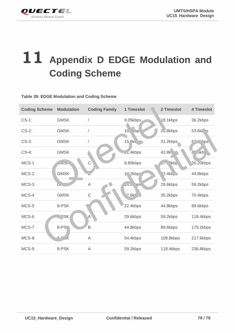
UMTS/HSPA Module UC15 Hardware Design
UC15_Hardware_Design Confidential / Released 79 / 79
11 Appendix D EDGE Modulation and
Coding Scheme
Table 39: EDGE Modulation and Coding Scheme
Coding Scheme Modulation Coding Family 1 Timeslot 2 Timeslot 4 Timeslot
CS-1: GMSK / 9.05kbps 18.1kbps 36.2kbps
CS-2: GMSK / 13.4kbps 26.8kbps 53.6kbps
CS-3: GMSK / 15.6kbps 31.2kbps 62.4kbps
CS-4: GMSK / 21.4kbps 42.8kbps 85.6kbps
MCS-1 GMSK C 8.80kbps 17.60kbps 35.20kbps
MCS-2 GMSK B 11.2kbps 22.4kbps 44.8kbps
MCS-3 GMSK A 14.8kbps 29.6kbps 59.2kbps
MCS-4 GMSK C 17.6kbps 35.2kbps 70.4kbps
MCS-5 8-PSK B 22.4kbps 44.8kbps 89.6kbps
MCS-6 8-PSK A 29.6kbps 59.2kbps 118.4kbps
MCS-7 8-PSK B 44.8kbps 89.6kbps 179.2kbps
MCS-8 8-PSK A 54.4kbps 108.8kbps 217.6kbps
MCS-9 8-PSK A 59.2kbps 118.4kbps 236.8kbps
Quectel
Confidential