Embed Size (px)
Citation preview
0
4
8
12
16
20
24
28
32
8 12 16 20
Supply Voltage (V)
Pro
pagation D
ela
y (
ns)
TDLRR
TDLFF
TDHRR
TDHFF
PWM CONTROLLER
12 V100 V
SECONDARYSIDE
CIRCUIT
HI
CO
NT
RO
L
DRIVELO
DRIVEHI
VDD
UCC27211A-Q1
VSS
LI
HB
HO
HS
LO
ISOLATION AND FEEDBACK
Product
Folder
Sample &Buy
Technical
Documents
Tools &
Software
Support &Community
UCC27211A-Q1SLUSCG0A –DECEMBER 2015–REVISED JANUARY 2016
UCC27211A-Q1 120-V Boot, 4-A Peak, High-Frequency High-Side and Low-Side Driver1 Features 2 Applications1• Qualified for Automotive Applications • Power Supplies for Telecom, Datacom, and
Merchant• AEC-Q100 Qualified With the Following Results:• Half-Bridge and Full-Bridge Converters– Device Temperature Grade –40°C to +140°C• Push-Pull ConvertersAmbient Operating Temperature Range• High Voltage Synchronous-Buck Converters– Device HBM Classification Level 2• Two-Switch Forward Converters– Device CDM Classification Level C6• Active-Clamp Forward Converters• Drives Two N-Channel MOSFETs in High-Side
and Low-Side Configuration With Independent • Class-D Audio AmplifiersInputs
3 Description• Maximum Boot Voltage 120-V DCThe UCC27211A-Q1 device driver is based on the• 4-A Sink, 4-A Source Output Currentspopular UCC27201 MOSFET drivers; but, this device• 0.9-Ω Pullup and Pulldown Resistance offers several significant performance improvements.
• Input Pins Can Tolerate –10 V to +20 V and areThe peak output pullup and pulldown current hasIndependent of Supply Voltage Rangebeen increased to 4-A source and 4-A sink, and• TTL Compatible Inputs pullup and pulldown resistance have been reduced to
• 8-V to 17-V VDD Operating Range, (20-V ABS 0.9 Ω, and thereby allows for driving large powerMAX) MOSFETs with minimized switching losses during the
transition through the Miller Plateau of the MOSFET.• 7.2-ns Rise and 5.5-ns Fall Time With 1000-pFThe input structure can directly handle –10 VDC,Loadwhich increases robustness and also allows direct
• Fast Propagation Delay Times (20-ns typical) interface to gate-drive transformers without using• 4-ns Delay Matching rectification diodes. The inputs are also independent
of supply voltage and have a 20-V maximum rating.• Symmetrical Undervoltage Lockout for High-Sideand Low-Side Driver
Device Information(1)
• Available in the Industry Standard SO-PowerPADPART NUMBER PACKAGE BODY SIZE (NOM)SOIC-8 Package
UCC27211A-Q1 SO PowerPAD™ (8) 4.89 mm × 3.90 mm• Specified from –40 to +140°C(1) For all available packages, see the orderable addendum at
the end of the data sheet.
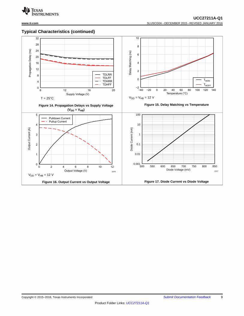
Typical Application Diagram Propagation Delays vs Supply VoltageT = 25°C
1
An IMPORTANT NOTICE at the end of this data sheet addresses availability, warranty, changes, use in safety-critical applications,intellectual property matters and other important disclaimers. PRODUCTION DATA.
UCC27211A-Q1SLUSCG0A –DECEMBER 2015–REVISED JANUARY 2016 www.ti.com
Table of Contents8.3 Feature Description................................................. 111 Features .................................................................. 18.4 Device Functional Modes........................................ 122 Applications ........................................................... 1
9 Application and Implementation ........................ 133 Description ............................................................. 19.1 Application Information............................................ 134 Revision History..................................................... 29.2 Typical Application .................................................. 135 Description (continued)......................................... 2
10 Power Supply Recommendations ..................... 186 Pin Configuration and Functions ......................... 311 Layout................................................................... 187 Specifications......................................................... 4
11.1 Layout Guidelines ................................................. 187.1 Absolute Maximum Ratings ...................................... 411.2 Layout Example .................................................... 197.2 ESD Ratings ............................................................ 411.3 Thermal Considerations ........................................ 197.3 Recommended Operating Conditions....................... 4
12 Device and Documentation Support ................. 207.4 Thermal Information .................................................. 512.1 Documentation Support ........................................ 207.5 Electrical Characteristics........................................... 512.2 Community Resources.......................................... 207.6 Switching Characteristics .......................................... 612.3 Trademarks ........................................................... 207.7 Typical Characteristics .............................................. 712.4 Electrostatic Discharge Caution............................ 208 Detailed Description ............................................ 1012.5 Glossary ................................................................ 208.1 Overview ................................................................. 10
13 Mechanical, Packaging, and Orderable8.2 Functional Block Diagram ....................................... 11Information ........................................................... 20
4 Revision HistoryNOTE: Page numbers for previous revisions may differ from page numbers in the current version.
DATE REVISION NOTESJanuary 2016 * Initial release.
5 Description (continued)The switching node of the UCC27211A-Q1 (HS pin) can handle –18-V maximum, which allows the high-sidechannel to be protected from inherent negative voltages caused by parasitic inductance and stray capacitance.The UCC27211A-Q1 has increased hysteresis that allows for interface to analog or digital PWM controllers withenhanced noise immunity.
The low-side and high-side gate drivers are independently controlled and matched to 2 ns between the turn onand turn off of each other.
An on-chip 120-V rated bootstrap diode eliminates the external discrete diodes. Undervoltage lockout is providedfor both the high-side and the low-side drivers which provides symmetric turn on and turn off behavior and forcesthe outputs low if the drive voltage is below the specified threshold.
The UCC27211A-Q1 device is offered in an 8-Pin SO-PowerPAD package.
2 Submit Documentation Feedback Copyright © 2015–2016, Texas Instruments Incorporated
Product Folder Links: UCC27211A-Q1
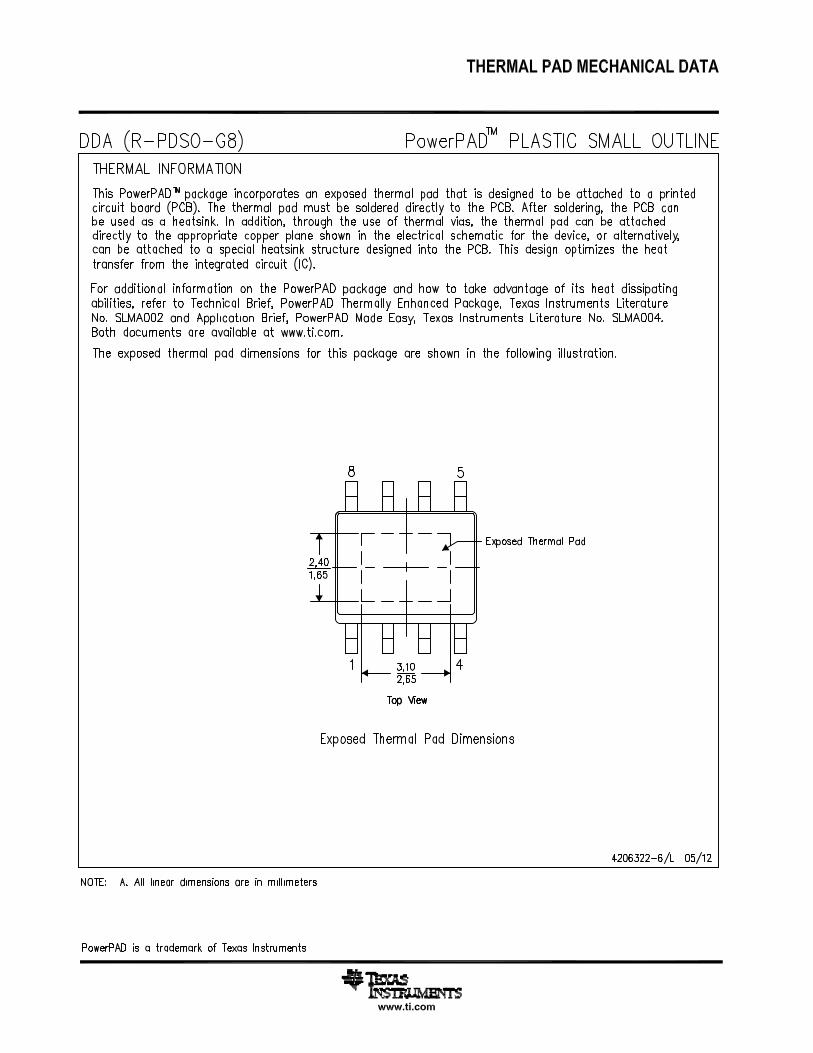
Thermal
Pad
1VDD 8 LO
2HB 7 VSS
3HO 6 LI
4HS 5 HI
UCC27211A-Q1www.ti.com SLUSCG0A –DECEMBER 2015–REVISED JANUARY 2016
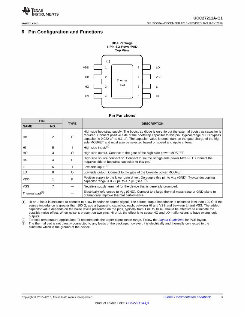
6 Pin Configuration and Functions
DDA Package8-Pin SO-PowerPAD
Top View
Pin FunctionsPIN
TYPE DESCRIPTIONNAME NO.
High-side bootstrap supply. The bootstrap diode is on-chip but the external bootstrap capacitor isrequired. Connect positive side of the bootstrap capacitor to this pin. Typical range of HB bypassHB 2 P capacitor is 0.022 µF to 0.1 µF. The capacitor value is dependant on the gate charge of the high-side MOSFET and must also be selected based on speed and ripple criteria.
HI 5 I High-side input. (1)
HO 3 O High-side output. Connect to the gate of the high-side power MOSFET.High-side source connection. Connect to source of high-side power MOSFET. Connect theHS 4 P negative side of bootstrap capacitor to this pin.
LI 6 I Low-side input. (1)
LO 8 O Low-side output. Connect to the gate of the low-side power MOSFET.Positive supply to the lower-gate driver. De-couple this pin to VSS (GND). Typical decouplingVDD 1 P capacitor range is 0.22 µF to 4.7 µF (See (2)).
VSS 7 — Negative supply terminal for the device that is generally grounded.Electrically referenced to VSS (GND). Connect to a large thermal mass trace or GND plane toThermal pad (3) — dramatically improve thermal performance.
(1) HI or LI input is assumed to connect to a low impedance source signal. The source output impedance is assumed less than 100 Ω. If thesource impedance is greater than 100 Ω, add a bypassing capacitor, each, between HI and VSS and between LI and VSS. The addedcapacitor value depends on the noise levels presented on the pins, typically from 1 nF to 10 nF should be effective to eliminate thepossible noise effect. When noise is present on two pins, HI or LI, the effect is to cause HO and LO malfunctions to have wrong logicoutputs.
(2) For cold temperature applications TI recommends the upper capacitance range. Follow the Layout Guidelines for PCB layout.(3) The thermal pad is not directly connected to any leads of the package; however, it is electrically and thermally connected to the
substrate which is the ground of the device.
Copyright © 2015–2016, Texas Instruments Incorporated Submit Documentation Feedback 3
Product Folder Links: UCC27211A-Q1
UCC27211A-Q1SLUSCG0A –DECEMBER 2015–REVISED JANUARY 2016 www.ti.com
7 Specifications
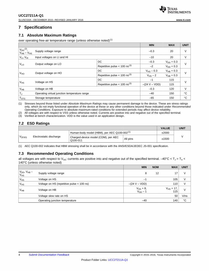
7.1 Absolute Maximum Ratingsover operating free-air temperature range (unless otherwise noted) (1)
MIN MAX UNITVDD
(2), Supply voltage range –0.3 20 VVHB – VHS
VLI, VHI Input voltages on LI and HI –10 20 VDC –0.3 VDD + 0.3
VLO Output voltage on LO VRepetitive pulse < 100 ns (3) –2 VDD + 0.3DC VHS – 0.3 VHB + 0.3
VHO Output voltage on HO VRepetitive pulse < 100 ns (3) VHS – 2 VHB + 0.3DC –1 115
VHS Voltage on HS VRepetitive pulse < 100 ns (3) –(24 V – VDD) 115
VHB Voltage on HB –0.3 120 VTJ Operating virtual junction temperature range –40 150 °CTSTG Storage temperature –65 150 °C
(1) Stresses beyond those listed under Absolute Maximum Ratings may cause permanent damage to the device. These are stress ratingsonly, which do not imply functional operation of the device at these or any other conditions beyond those indicated under RecommendedOperating Conditions. Exposure to absolute-maximum-rated conditions for extended periods may affect device reliability.
(2) All voltages are with respect to VSS unless otherwise noted. Currents are positive into and negative out of the specified terminal.(3) Verified at bench characterization. VDD is the value used in an application design.
7.2 ESD RatingsVALUE UNIT
Human-body model (HBM), per AEC Q100-002 (1) ±2000V(ESD) Electrostatic discharge VCharged-device model (CDM), per AEC All pins ±1500Q100-011
(1) AEC Q100-002 indicates that HBM stressing shall be in accordance with the ANSI/ESDA/JEDEC JS-001 specification.
7.3 Recommended Operating Conditionsall voltages are with respect to VSS; currents are positive into and negative out of the specified terminal. –40°C < TJ = TA <140°C (unless otherwise noted)
MIN NOM MAX UNITVDD, VHB – Supply voltage range 8 12 17 VVHS
VHS Voltage on HS –1 105 VVHS Voltage on HS (repetitive pulse < 100 ns) –(24 V – VDD) 110 V
VHS + 8, VHS + 17,VHB Voltage on HB VVDD – 1 115Voltage slew rate on HS 50 V/nsOperating junction temperature –40 140 °C
4 Submit Documentation Feedback Copyright © 2015–2016, Texas Instruments Incorporated
Product Folder Links: UCC27211A-Q1
UCC27211A-Q1www.ti.com SLUSCG0A –DECEMBER 2015–REVISED JANUARY 2016
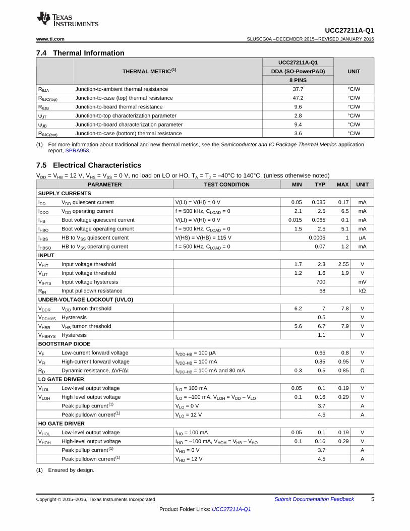
7.4 Thermal InformationUCC27211A-Q1
THERMAL METRIC (1) DDA (SO-PowerPAD) UNIT8 PINS
RθJA Junction-to-ambient thermal resistance 37.7 °C/WRθJC(top) Junction-to-case (top) thermal resistance 47.2 °C/WRθJB Junction-to-board thermal resistance 9.6 °C/WψJT Junction-to-top characterization parameter 2.8 °C/WψJB Junction-to-board characterization parameter 9.4 °C/WRθJC(bot) Junction-to-case (bottom) thermal resistance 3.6 °C/W
(1) For more information about traditional and new thermal metrics, see the Semiconductor and IC Package Thermal Metrics applicationreport, SPRA953.
7.5 Electrical CharacteristicsVDD = VHB = 12 V, VHS = VSS = 0 V, no load on LO or HO, TA = TJ = –40°C to 140°C, (unless otherwise noted)
PARAMETER TEST CONDITION MIN TYP MAX UNITSUPPLY CURRENTSIDD VDD quiescent current V(LI) = V(HI) = 0 V 0.05 0.085 0.17 mAIDDO VDD operating current f = 500 kHz, CLOAD = 0 2.1 2.5 6.5 mAIHB Boot voltage quiescent current V(LI) = V(HI) = 0 V 0.015 0.065 0.1 mAIHBO Boot voltage operating current f = 500 kHz, CLOAD = 0 1.5 2.5 5.1 mAIHBS HB to VSS quiescent current V(HS) = V(HB) = 115 V 0.0005 1 µAIHBSO HB to VSS operating current f = 500 kHz, CLOAD = 0 0.07 1.2 mAINPUTVHIT Input voltage threshold 1.7 2.3 2.55 VVLIT Input voltage threshold 1.2 1.6 1.9 VVIHYS Input voltage hysteresis 700 mVRIN Input pulldown resistance 68 kΩUNDER-VOLTAGE LOCKOUT (UVLO)VDDR VDD turnon threshold 6.2 7 7.8 VVDDHYS Hysteresis 0.5 VVHBR VHB turnon threshold 5.6 6.7 7.9 VVHBHYS Hysteresis 1.1 VBOOTSTRAP DIODEVF Low-current forward voltage IVDD-HB = 100 µA 0.65 0.8 VVFI High-current forward voltage IVDD-HB = 100 mA 0.85 0.95 VRD Dynamic resistance, ΔVF/ΔI IVDD-HB = 100 mA and 80 mA 0.3 0.5 0.85 ΩLO GATE DRIVERVLOL Low-level output voltage ILO = 100 mA 0.05 0.1 0.19 VVLOH High level output voltage ILO = –100 mA, VLOH = VDD – VLO 0.1 0.16 0.29 V
Peak pullup current (1) VLO = 0 V 3.7 APeak pulldown current (1) VLO = 12 V 4.5 A
HO GATE DRIVERVHOL Low-level output voltage IHO = 100 mA 0.05 0.1 0.19 VVHOH High-level output voltage IHO = –100 mA, VHOH = VHB – VHO 0.1 0.16 0.29 V
Peak pullup current (1) VHO = 0 V 3.7 APeak pulldown current (1) VHO = 12 V 4.5 A
(1) Ensured by design.
Copyright © 2015–2016, Texas Instruments Incorporated Submit Documentation Feedback 5
Product Folder Links: UCC27211A-Q1
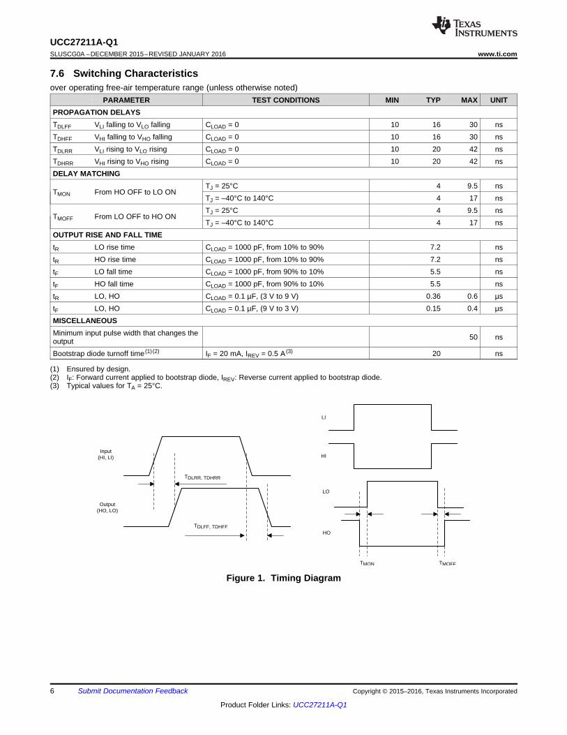
Input(HI, LI)
Output(HO, LO)
TMON TMOFF
LI
HI
LO
HO
TDLRR, TDHRR
TDLFF, TDHFF
UCC27211A-Q1SLUSCG0A –DECEMBER 2015–REVISED JANUARY 2016 www.ti.com
7.6 Switching Characteristicsover operating free-air temperature range (unless otherwise noted)
PARAMETER TEST CONDITIONS MIN TYP MAX UNITPROPAGATION DELAYSTDLFF VLI falling to VLO falling CLOAD = 0 10 16 30 nsTDHFF VHI falling to VHO falling CLOAD = 0 10 16 30 nsTDLRR VLI rising to VLO rising CLOAD = 0 10 20 42 nsTDHRR VHI rising to VHO rising CLOAD = 0 10 20 42 nsDELAY MATCHING
TJ = 25°C 4 9.5 nsTMON From HO OFF to LO ON
TJ = –40°C to 140°C 4 17 nsTJ = 25°C 4 9.5 ns
TMOFF From LO OFF to HO ONTJ = –40°C to 140°C 4 17 ns
OUTPUT RISE AND FALL TIMEtR LO rise time CLOAD = 1000 pF, from 10% to 90% 7.2 nstR HO rise time CLOAD = 1000 pF, from 10% to 90% 7.2 nstF LO fall time CLOAD = 1000 pF, from 90% to 10% 5.5 nstF HO fall time CLOAD = 1000 pF, from 90% to 10% 5.5 nstR LO, HO CLOAD = 0.1 µF, (3 V to 9 V) 0.36 0.6 µstF LO, HO CLOAD = 0.1 µF, (9 V to 3 V) 0.15 0.4 µsMISCELLANEOUSMinimum input pulse width that changes the 50 nsoutputBootstrap diode turnoff time (1) (2) IF = 20 mA, IREV = 0.5 A (3) 20 ns
(1) Ensured by design.(2) IF: Forward current applied to bootstrap diode, IREV: Reverse current applied to bootstrap diode.(3) Typical values for TA = 25°C.
Figure 1. Timing Diagram
6 Submit Documentation Feedback Copyright © 2015–2016, Texas Instruments Incorporated
Product Folder Links: UCC27211A-Q1
−1
0
1
2
3
4
5
6
8 12 16 20
Supply Voltage (V)
InputT
hre
shold
Voltage (V
)
Rising
Falling−1
0
1
2
3
4
5
6
−40 −20 0 20 40 60 80 100 120 140
Temperature (°C)
InputT
hre
shold
Voltage (V
)
Rising
Falling
0.01
0.1
1
10
100
10 100 1000
Frequency (kHz)
IDD
Op
era
tin
g C
urr
en
t (m
A)
C = 0 pF, T = −40°CL
CL = 0 pF, T = 25°C
CL = 0 pF, T = 140°C
CL = 1000 pF, T = 25°C
CL = 1000 pF, T = 140°C
CL = 4700 pF, T = 140°C0.01
0.1
1
10
100
10 100 1000
Frequency (kHz)
Bo
ot
Op
era
tin
g C
urr
en
t (m
A)
C = 0 pF, T = −40°CL
CL = 0 pF, T = 25°C
CL = 0 pF, T = 140°C
CL = 1000 pF, T = 25°C
CL = 1000 pF, T = 140°C
CL = 4700 pF, T = 140°C
0
20
40
60
80
100
0 2 4 6 8 10 12 14 16 18 20
Supply Voltage (V)
Qu
iesce
nt
Cu
rre
nt
(µA
)
IDD
IHB
0.01
0.1
1
10
100
10 100 1000
Frequency (kHz)
IDD
Opera
ting C
urr
ent (m
A)
C = 0 pF, T = −40°CL
CL = 0 pF, T = 25°C
CL = 0 pF, T = 140°C
CL = 1000 pF, T = 25°C
CL = 1000 pF, T = 140°C
CL = 4700 pF, T = 140°C
G002
UCC27211A-Q1www.ti.com SLUSCG0A –DECEMBER 2015–REVISED JANUARY 2016
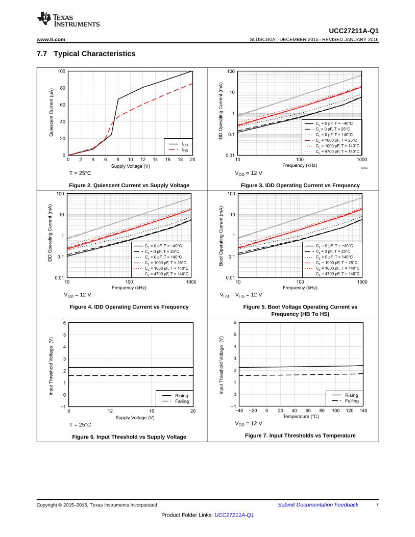
7.7 Typical Characteristics
T = 25°C VDD = 12 V
Figure 2. Quiescent Current vs Supply Voltage Figure 3. IDD Operating Current vs Frequency
VDD = 12 V VHB – VHS = 12 V
Figure 4. IDD Operating Current vs Frequency Figure 5. Boot Voltage Operating Current vsFrequency (HB To HS)
VDD = 12 VT = 25°C
Figure 7. Input Thresholds vs TemperatureFigure 6. Input Threshold vs Supply Voltage
Copyright © 2015–2016, Texas Instruments Incorporated Submit Documentation Feedback 7
Product Folder Links: UCC27211A-Q1
0
4
8
12
16
20
24
28
32
36
40
−40 −20 0 20 40 60 80 100 120 140
Temperature (°C)
Pro
pagation D
ela
y (
ns)
TDLRR
TDLFF
TDHRR
TDHFF
0
8
16
24
32
−40 −20 0 20 40 60 80 100 120 140
Temperature (°C)
Pro
pagation D
ela
y (
ns)
TDLRR
TDLFF
TDHRR
TDHFF
5.2
5.6
6
6.4
6.8
7.2
7.6
8
−40 −20 0 20 40 60 80 100 120 140Temperature (°C)
Thr
esho
ld (
V)
VDD Rising ThresholdHB Rising Threshold
G009
0
0.3
0.6
0.9
1.2
1.5
−40 −20 0 20 40 60 80 100 120 140Temperature (°C)
Hys
tere
sis
(V)
VDD UVLO HysteresisHB UVLO Hysteresis
G010
0
0.04
0.08
0.12
0.16
0.2
0.24
0.28
0.32
−40 −20 0 20 40 60 80 100 120 140
Temperature (°C)
V–
LO
/HO
Ou
tpu
t V
olta
ge
(V
)O
H
V = V = 8 VDD HB
V = V = 12 VDD HB
V = V = 16 VDD HB
V = V = 20 VDD HB
0
0.04
0.08
0.12
0.16
0.2
−40 −20 0 20 40 60 80 100 120 140
Temperature (°C)
VO
L−
LO
/HO
Ou
tpu
t V
olta
ge
(V
)
V = V = 8 VDD HB
V = V = 12 VDD HB
V = V = 16 VDD HB
V = V = 20 VDD HB
UCC27211A-Q1SLUSCG0A –DECEMBER 2015–REVISED JANUARY 2016 www.ti.com
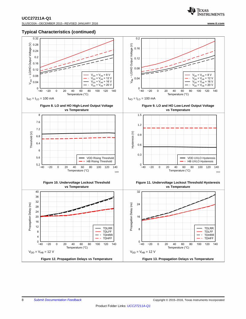
Typical Characteristics (continued)
IHO = ILO = 100 mA IHO = ILO = 100 mA
Figure 8. LO and HO High-Level Output Voltage Figure 9. LO and HO Low-Level Output Voltagevs Temperature vs Temperature
Figure 10. Undervoltage Lockout Threshold Figure 11. Undervoltage Lockout Threshold Hysteresisvs Temperature vs Temperature
VDD = VHB = 12 V VDD = VHB = 12 V
Figure 12. Propagation Delays vs Temperature Figure 13. Propagation Delays vs Temperature
8 Submit Documentation Feedback Copyright © 2015–2016, Texas Instruments Incorporated
Product Folder Links: UCC27211A-Q1
0
1
2
3
4
5
0 2 4 6 8 10 12
Output Voltage (V)
Outp
ut C
urr
ent (A
)
Pulldown Current
Pullup Current
G016
0.001
0.01
0.1
1
10
100
500 550 600 650 700 750 800 850Diode Voltage (mV)
Dio
de C
urre
nt (
mA
)
G017
0
4
8
12
16
20
24
28
32
8 12 16 20
Supply Voltage (V)
Pro
pagation D
ela
y (
ns)
TDLRR
TDLFF
TDHRR
TDHFF−2
0
2
4
6
8
10
−40 −20 0 20 40 60 80 100 120 140
Temperature (°C)
Dela
y M
atc
hin
g (
ns)
TMON
TMOFF
UCC27211A-Q1www.ti.com SLUSCG0A –DECEMBER 2015–REVISED JANUARY 2016
Typical Characteristics (continued)
VDD = VHB = 12 VT = 25°C
Figure 15. Delay Matching vs TemperatureFigure 14. Propagation Delays vs Supply Voltage(VDD = VHB)
VDD = VHB = 12 V
Figure 17. Diode Current vs Diode VoltageFigure 16. Output Current vs Output Voltage
Copyright © 2015–2016, Texas Instruments Incorporated Submit Documentation Feedback 9
Product Folder Links: UCC27211A-Q1
UCC27211A-Q1SLUSCG0A –DECEMBER 2015–REVISED JANUARY 2016 www.ti.com
8 Detailed Description
8.1 OverviewThe UCC2721A-Q1 device represents Texas Instruments’ latest generation of high-voltage gate drivers, whichare designed to drive both the high-side and low-side of N-Channel MOSFETs in a half- and full-bridge orsynchronous-buck configuration. The floating high-side driver can operate with supply voltages of up to 120 V,which allows for N-Channel MOSFET control in half-bridge, full-bridge, push-pull, two-switch forward, and activeclamp forward converters.
The UCC27211A-Q1 device features 4-A source and sink capability, industry best-in-class switchingcharacteristics and a host of other features listed in Table 1. These features combine to ensure efficient, robustand reliable operation in high-frequency switching power circuits.
Table 1. UCC27211A-Q1 HighlightsFEATURE BENEFIT
High peak current ideal for driving large power MOSFETs with4-A source and sink current with 0.9-Ω output resistance minimal power loss (fast-drive capability at Miller plateau)Increased robustness and ability to handle undershoot and
Input pins (HI and LI) can directly handle –10 VDC up to 20 VDC overshoot can interface directly to gate-drive transformers withouthaving to use rectification diodes.
120-V internal boot diode Provides voltage margin to meet telecom 100-V surge requirementsAllows the high-side channel to have extra protection from inherent
Switch node (HS pin) able to handle –18 V maximum for 100 ns negative voltages caused by parasitic inductance and straycapacitance
Robust ESD circuitry to handle voltage spikes Excellent immunity to large dV/dT conditionsBest-in-class switching characteristics and extremely low-pulse18-ns propagation delay with 7.2-ns rise time and 5.5-ns fall time transmission distortion
2-ns (typical) delay matching between channels Avoids transformer volt-second offset in bridgeSymmetrical UVLO circuit Ensures high-side and low-side shut down at the same time
Complementary to analog or digital PWM controllers; increasedTTL optimized thresholds with increased hysteresis hysteresis offers added noise immunity
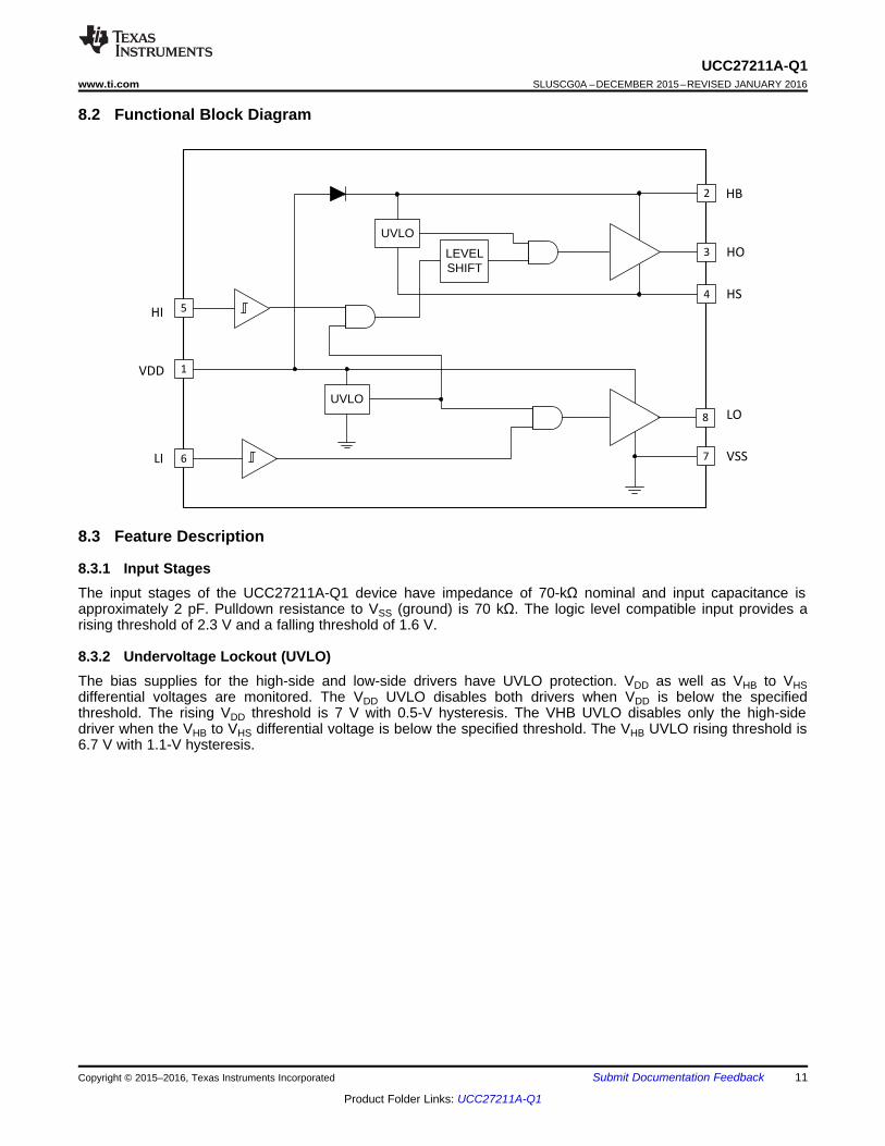
In the UCC27211A-Q1 device, the high side and low side each have independent inputs that allow maximumflexibility of input control signals in the application. The boot diode for the high-side driver bias supply is internalto the UCC27211A. The UCC27211A is a TTL or logic compatible device. The high-side driver is referenced tothe switch node (HS), which is typically the source pin of the high-side MOSFET and drain pin of the low-sideMOSFET. The low-side driver is referenced to VSS, which is typically ground. The UCC27211A-Q1 functions aredivided into the input stages, UVLO protection, level shift, boot diode, and output driver stages.
10 Submit Documentation Feedback Copyright © 2015–2016, Texas Instruments Incorporated
Product Folder Links: UCC27211A-Q1
LEVEL SHIFT
UVLO
UVLO
5
3
8
4
6 7
2
1
HI
LI
VDD
HB
HO
HS
LO
VSS
UCC27211A-Q1www.ti.com SLUSCG0A –DECEMBER 2015–REVISED JANUARY 2016
8.2 Functional Block Diagram
8.3 Feature Description
8.3.1 Input StagesThe input stages of the UCC27211A-Q1 device have impedance of 70-kΩ nominal and input capacitance isapproximately 2 pF. Pulldown resistance to VSS (ground) is 70 kΩ. The logic level compatible input provides arising threshold of 2.3 V and a falling threshold of 1.6 V.
8.3.2 Undervoltage Lockout (UVLO)The bias supplies for the high-side and low-side drivers have UVLO protection. VDD as well as VHB to VHSdifferential voltages are monitored. The VDD UVLO disables both drivers when VDD is below the specifiedthreshold. The rising VDD threshold is 7 V with 0.5-V hysteresis. The VHB UVLO disables only the high-sidedriver when the VHB to VHS differential voltage is below the specified threshold. The VHB UVLO rising threshold is6.7 V with 1.1-V hysteresis.
Copyright © 2015–2016, Texas Instruments Incorporated Submit Documentation Feedback 11
Product Folder Links: UCC27211A-Q1
UCC27211A-Q1SLUSCG0A –DECEMBER 2015–REVISED JANUARY 2016 www.ti.com
Feature Description (continued)8.3.3 Level ShiftThe level shift circuit is the interface from the high-side input to the high-side driver stage which is referenced tothe switch node (HS). The level shift allows control of the HO output referenced to the HS pin and providesexcellent delay matching with the low-side driver.
8.3.4 Boot DiodeThe boot diode necessary to generate the high-side bias is included in the UCC27211A-Q1 family of drivers. Thediode anode is connected to VDD and cathode connected to VHB. With the VHB capacitor connected to HB and theHS pins, the VHB capacitor charge is refreshed every switching cycle when HS transitions to ground. The bootdiode provides fast recovery times, low diode resistance, and voltage rating margin to allow for efficient andreliable operation.
8.3.5 Output StagesThe output stages are the interface to the power MOSFETs in the power train. High slew rate, low resistance andhigh peak current capability of both output drivers allow for efficient switching of the power MOSFETs. The low-side output stage is referenced from VDD to VSS and the high side is referenced from VHB to VHS.
8.4 Device Functional ModesThe device operates in normal mode and UVLO mode. See the Undervoltage Lockout (UVLO) section forinformation on UVLO operation mode. In the normal mode the output state is dependent on states of the HI andLI pins. Table 2 lists the output states for different input pin combinations.
Table 2. Device Logic TableHI PIN LI PIN HO (1) LO (2)
L L L LL H L HH L H LH H H H
(1) HO is measured with respect to HS.(2) LO is measured with respect to VSS.
12 Submit Documentation Feedback Copyright © 2015–2016, Texas Instruments Incorporated
Product Folder Links: UCC27211A-Q1
PWM CONTROLLER
12 V100 V
SECONDARYSIDE
CIRCUIT
HI
CO
NT
RO
L
DRIVELO
DRIVEHI
VDD
UCC27211A-Q1
VSS
LI
HB
HO
HS
LO
ISOLATION AND FEEDBACK
UCC27211A-Q1www.ti.com SLUSCG0A –DECEMBER 2015–REVISED JANUARY 2016
9 Application and Implementation
NOTEInformation in the following applications sections is not part of the TI componentspecification, and TI does not warrant its accuracy or completeness. TI’s customers areresponsible for determining suitability of components for their purposes. Customers shouldvalidate and test their design implementation to confirm system functionality.
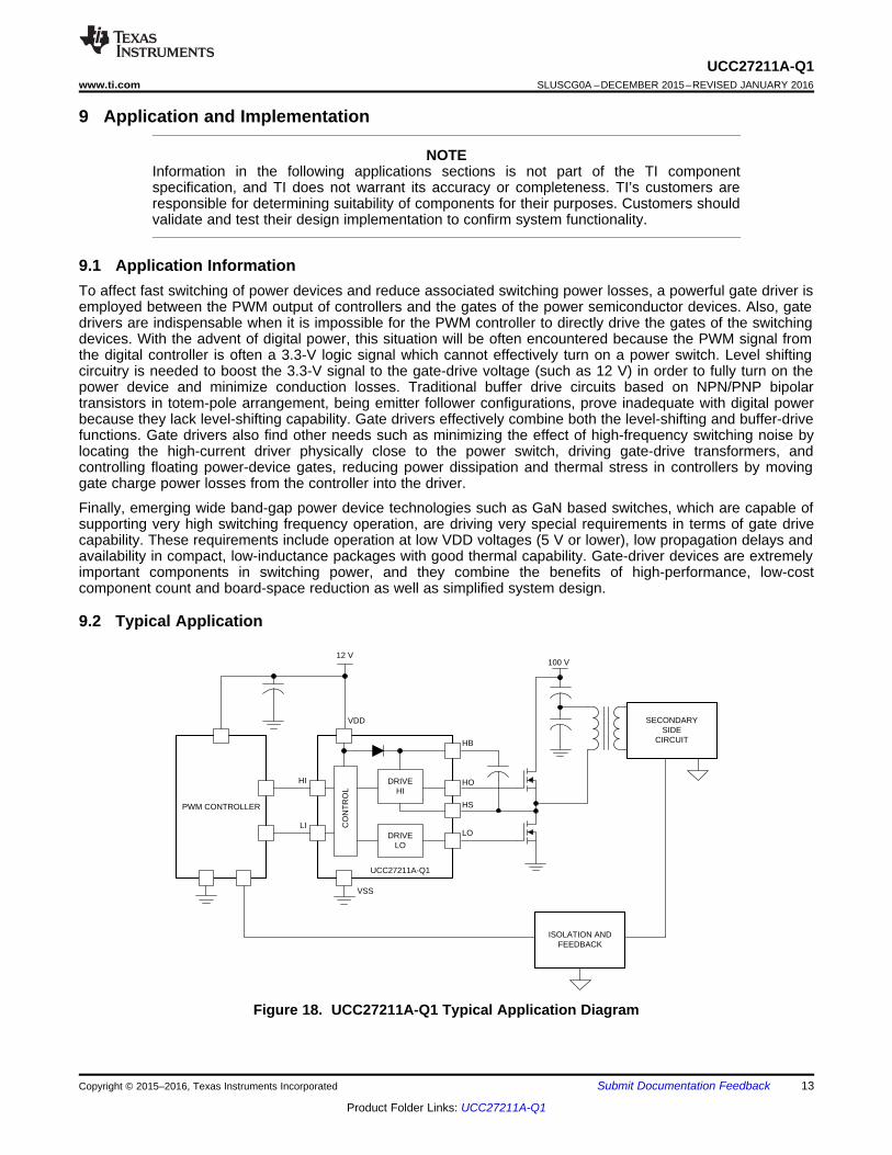
9.1 Application InformationTo affect fast switching of power devices and reduce associated switching power losses, a powerful gate driver isemployed between the PWM output of controllers and the gates of the power semiconductor devices. Also, gatedrivers are indispensable when it is impossible for the PWM controller to directly drive the gates of the switchingdevices. With the advent of digital power, this situation will be often encountered because the PWM signal fromthe digital controller is often a 3.3-V logic signal which cannot effectively turn on a power switch. Level shiftingcircuitry is needed to boost the 3.3-V signal to the gate-drive voltage (such as 12 V) in order to fully turn on thepower device and minimize conduction losses. Traditional buffer drive circuits based on NPN/PNP bipolartransistors in totem-pole arrangement, being emitter follower configurations, prove inadequate with digital powerbecause they lack level-shifting capability. Gate drivers effectively combine both the level-shifting and buffer-drivefunctions. Gate drivers also find other needs such as minimizing the effect of high-frequency switching noise bylocating the high-current driver physically close to the power switch, driving gate-drive transformers, andcontrolling floating power-device gates, reducing power dissipation and thermal stress in controllers by movinggate charge power losses from the controller into the driver.
Finally, emerging wide band-gap power device technologies such as GaN based switches, which are capable ofsupporting very high switching frequency operation, are driving very special requirements in terms of gate drivecapability. These requirements include operation at low VDD voltages (5 V or lower), low propagation delays andavailability in compact, low-inductance packages with good thermal capability. Gate-driver devices are extremelyimportant components in switching power, and they combine the benefits of high-performance, low-costcomponent count and board-space reduction as well as simplified system design.
9.2 Typical Application
Figure 18. UCC27211A-Q1 Typical Application Diagram
Copyright © 2015–2016, Texas Instruments Incorporated Submit Documentation Feedback 13
Product Folder Links: UCC27211A-Q1
PWM CONTROLLER
12 V
100 V SECONDARYSIDE
CIRCUIT
HI
CO
NT
RO
L
DRIVELO
DRIVEHI
VDD
UCC27211A-Q1
VSS
LI
HB
HO
HS
LO
12 V
HI
CO
NT
RO
L
DRIVELO
DRIVEHI
VDD
UCC27211A-Q1
LI
HB
HO
HS
LO
100 V
UCC27211A-Q1SLUSCG0A –DECEMBER 2015–REVISED JANUARY 2016 www.ti.com
Typical Application (continued)
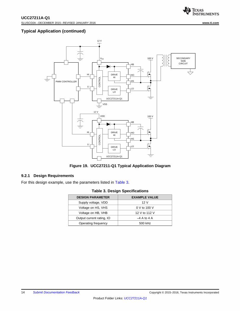
Figure 19. UCC27211-Q1 Typical Application Diagram
9.2.1 Design RequirementsFor this design example, use the parameters listed in Table 3.
Table 3. Design SpecificationsDESIGN PARAMETER EXAMPLE VALUE
Supply voltage, VDD 12 VVoltage on HS, VHS 0 V to 100 VVoltage on HB, VHB 12 V to 112 V
Output current rating, IO –4 A to 4 AOperating frequency 500 kHz
14 Submit Documentation Feedback Copyright © 2015–2016, Texas Instruments Incorporated
Product Folder Links: UCC27211A-Q1
UCC27211A-Q1www.ti.com SLUSCG0A –DECEMBER 2015–REVISED JANUARY 2016
9.2.2 Detailed Design Procedure
9.2.2.1 Input Threshold TypeThe UCC27211A-Q1 device has an input maximum voltage range from –10 V to 20 V. This increased robustnessmeans that both parts can be directly interfaced to gate drive transformers. The UCC27211A-Q1 device featuresTTL compatible input threshold logic with wide hysteresis. The threshold voltage levels are low voltage andindependent of the VDD supply voltage, which allows compatibility with both logic-level input signals frommicrocontrollers as well as higher-voltage input signals from analog controllers. See the Electrical Characteristicstable for the actual input threshold voltage levels and hysteresis specifications for the UCC27211A-Q1 device.
9.2.2.2 VDD Bias Supply VoltageThe bias supply voltage to be applied to the VDD pin of the device should never exceed the values listed in theAbsolute Maximum Ratings table. However, different power switches demand different voltage levels to beapplied at the gate terminals for effective turnon and turnoff. With certain power switches, a positive gate voltagemay be required for turnon and a negative gate voltage may be required for turnoff, in which case the VDD biassupply equals the voltage differential. With a wide operating range from 8 V to 17 V, the UCC27211A-Q1 devicecan be used to drive a variety of power switches, such as Si MOSFETs, IGBTs, and wide-bandgap powersemiconductors (such as GaN, certain types of which allow no higher than 6 V to be applied to the gateterminals).
9.2.2.3 Peak Source and Sink CurrentsGenerally, the switching speed of the power switch during turnon and turnoff should be as fast as possible inorder to minimize switching power losses. The gate driver device must be able to provide the required peakcurrent for achieving the targeted switching speeds with the targeted power MOSFET. The system requirementfor the switching speed is typically described in terms of the slew rate of the drain-to-source voltage of the powerMOSFET (such as dVDS/dt). For example, the system requirement might state that a SPP20N60C3 powerMOSFET must be turned-on with a dVDS/dt of 20 V/ns or higher with a DC bus voltage of 400 V in a continuous-conduction-mode (CCM) boost PFC-converter application. This type of application is an inductive hard-switchingapplication and reducing switching power losses is critical. This requirement means that the entire drain-to-source voltage swing during power MOSFET turnon event (from 400 V in the OFF state to VDS(on) in on state)must be completed in approximately 20 ns or less. When the drain-to-source voltage swing occurs, the Millercharge of the power MOSFET (QGD parameter in the SPP20N60C3 data sheet is 33 nC typical) is supplied bythe peak current of gate driver. According to power MOSFET inductive switching mechanism, the gate-to-sourcevoltage of the power MOSFET at this time is the Miller plateau voltage, which is typically a few volts higher thanthe threshold voltage of the power MOSFET, VGS(TH).
To achieve the targeted dVDS/dt, the gate driver must be capable of providing the QGD charge in 20 ns or less. Inother words a peak current of 1.65 A (= 33 nC / 20 ns) or higher must be provided by the gate driver. TheUCC27211A gate driver is capable of providing 4-A peak sourcing current which clearly exceeds the designrequirement and has the capability to meet the switching speed needed. The 2.4× overdrive capability providesan extra margin against part-to-part variations in the QGD parameter of the power MOSFET along with additionalflexibility to insert external gate resistors and fine tune the switching speed for efficiency versus EMIoptimizations. However, in practical designs the parasitic trace inductance in the gate drive circuit of the PCB willhave a definitive role to play on the power MOSFET switching speed. The effect of this trace inductance is tolimit the dI/dt of the output current pulse of the gate driver. In order to illustrate this, consider output current pulsewaveform from the gate driver to be approximated to a triangular profile, where the area under the triangle(½ × IPEAK × time) would equal the total gate charge of the power MOSFET (QG parameter in SPP20N60C3power MOSFET datasheet = 87 nC typical). If the parasitic trace inductance limits the dI/dt then a situation mayoccur in which the full peak current capability of the gate driver is not fully achieved in the time required to deliverthe QG required for the power MOSFET switching. In other words the time parameter in the equation woulddominate and the IPEAK value of the current pulse would be much less than the true peak current capability of thedevice, while the required QG is still delivered. Because of this, the desired switching speed may not be realized,even when theoretical calculations indicate the gate driver is capable of achieving the targeted switching speed.Thus, placing the gate driver device very close to the power MOSFET and designing a tight gate drive-loop withminimal PCB trace inductance is important to realize the full peak-current capability of the gate driver.
Copyright © 2015–2016, Texas Instruments Incorporated Submit Documentation Feedback 15
Product Folder Links: UCC27211A-Q1
UCC27211A-Q1SLUSCG0A –DECEMBER 2015–REVISED JANUARY 2016 www.ti.com
9.2.2.4 Propagation DelayThe acceptable propagation delay from the gate driver is dependent on the switching frequency at which it isused and the acceptable level of pulse distortion to the system. The UCC27211A-Q1 device features 16-ns(typical) propagation delays, which ensures very little pulse distortion and allows operation at very high-frequencies. See the Electrical Characteristics table for the propagation and switching characteristics of theUCC27211A-Q1 device.
9.2.2.5 Power DissipationPower dissipation of the gate driver has two portions as shown in Equation 1.
PDISS = PDC + PSW (1)
Use Equation 2 to calculate the DC portion of the power dissipation (PDC).PDC = IQ × VDD
where• IQ is the quiescent current for the driver. (2)
The quiescent current is the current consumed by the device to bias all internal circuits such as input stage,reference voltage, logic circuits, protections, and also any current associated with switching of internal deviceswhen the driver output changes state (such as charging and discharging of parasitic capacitances, parasiticshoot-through, and so forth). The UCC27211A-Q1 features very low quiescent currents (less than 0.17 mA, referto the Electrical Characteristics table and contain internal logic to eliminate any shoot-through in the output driverstage. Thus the effect of the PDC on the total power dissipation within the gate driver can be safely assumed tobe negligible. The power dissipated in the gate-driver package during switching (PSW) depends on the followingfactors:• Gate charge required of the power device (usually a function of the drive voltage VG, which is very close to
input bias supply voltage VDD)• Switching frequency• Use of external gate resistors. When a driver device is tested with a discrete, capacitive load calculating the
power that is required from the bias supply is fairly simple. The energy that must be transferred from the biassupply to charge the capacitor is given by Equation 3.
EG = ½CLOAD × VDD2
where• CLOAD is load capacitor• VDD is bias voltage feeding the driver (3)
There is an equal amount of energy dissipated when the capacitor is charged and when it is discharged. Thisleads to a total power loss given by Equation 4.
PG = CLOAD × VDD2 × fSW
where• fSW is the switching frequency (4)
The switching load presented by a power MOSFET/IGBT is converted to an equivalent capacitance by examiningthe gate charge required to switch the device. This gate charge includes the effects of the input capacitance plusthe added charge needed to swing the drain voltage of the power device as it switches between the ON and OFFstates. Most manufacturers provide specifications of typical and maximum gate charge, in nC, to switch thedevice under specified conditions. Using the gate charge Qg, determine the power that must be dissipated whenswitching a capacitor which is calculated using the equation QG = CLOAD × VDD to provide Equation 5 for power.
PG = CLOAD × VDD2 × fSW = QG × VDD × fSW (5)
This power PG is dissipated in the resistive elements of the circuit when the MOSFET/IGBT is being turned onand off. Half of the total power is dissipated when the load capacitor is charged during turnon, and the other halfis dissipated when the load capacitor is discharged during turnoff. When no external gate resistor is employedbetween the driver and MOSFET/IGBT, this power is completely dissipated inside the driver package. With theuse of external gate-drive resistors, the power dissipation is shared between the internal resistance of driver andexternal gate resistor.
16 Submit Documentation Feedback Copyright © 2015–2016, Texas Instruments Incorporated
Product Folder Links: UCC27211A-Q1
UCC27211A-Q1www.ti.com SLUSCG0A –DECEMBER 2015–REVISED JANUARY 2016
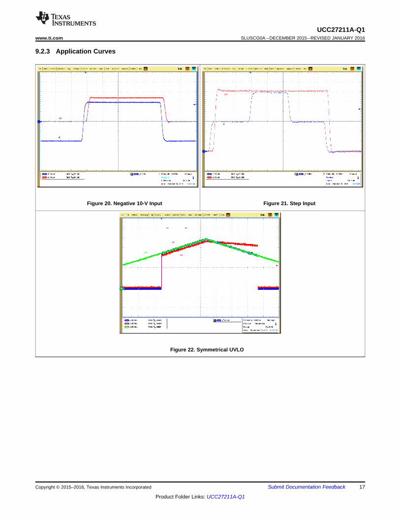
9.2.3 Application Curves
Figure 20. Negative 10-V Input Figure 21. Step Input
Figure 22. Symmetrical UVLO
Copyright © 2015–2016, Texas Instruments Incorporated Submit Documentation Feedback 17
Product Folder Links: UCC27211A-Q1
UCC27211A-Q1SLUSCG0A –DECEMBER 2015–REVISED JANUARY 2016 www.ti.com
10 Power Supply RecommendationsThe bias supply voltage range for which the UCC27211A-Q1 device is recommended to operate is from 8 V to17 V. The lower end of this range is governed by the internal undervoltage-lockout (UVLO) protection feature onthe VDD pin supply circuit blocks. Whenever the driver is in UVLO condition when the VDD pin voltage is belowthe V(ON) supply start threshold, this feature holds the output low, regardless of the status of the inputs. Theupper end of this range is driven by the 20-V absolute maximum voltage rating of the VDD pin of the device(which is a stress rating). Keeping a 3-V margin to allow for transient voltage spikes, the maximumrecommended voltage for the VDD pin is 17 V. The UVLO protection feature also involves a hysteresis function,which means that when the VDD pin bias voltage has exceeded the threshold voltage and device begins tooperate, and if the voltage drops, then the device continues to deliver normal functionality unless the voltagedrop exceeds the hysteresis specification VDD(hys). Therefore, ensuring that, while operating at or near the 8-Vrange, the voltage ripple on the auxiliary power supply output is smaller than the hysteresis specification of thedevice is important to avoid triggering device shutdown. During system shutdown, the device operation continuesuntil the VDD pin voltage has dropped below the V(OFF) threshold, which must be accounted for while evaluatingsystem shutdown timing design requirements. Likewise, at system start-up the device does not begin operationuntil the VDD pin voltage has exceeded the V(ON) threshold.
The quiescent current consumed by the internal circuit blocks of the device is supplied through the VDD pin.Although this fact is well known, it is important to recognize that the charge for source current pulses delivered bythe HO pin is also supplied through the same VDD pin. As a result, every time a current is sourced out of the HOpin, a corresponding current pulse is delivered into the device through the VDD pin. Thus, ensure that a localbypass capacitor is provided between the VDD and GND pins and located as close to the device as possible forthe purpose of decoupling is important. A lo-ESR, ceramic surface-mount capacitor is required. TI recommendsusing a capacitor in the range 0.22 µF to 4.7 µF between VDD and GND. In a similar manner, the current pulsesdelivered by the LO pin are sourced from the HB pin. Therefore a 0.022-µF to 0.1-µF local decoupling capacitoris recommended between the HB and HS pins.
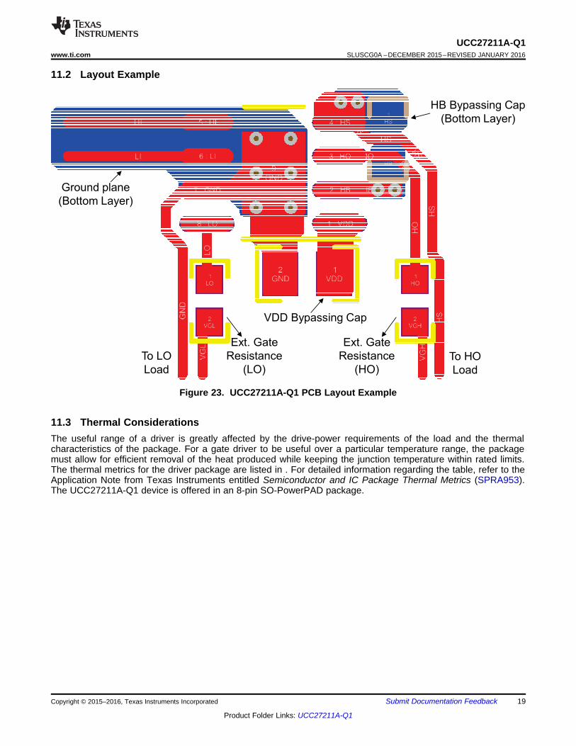
11 Layout
11.1 Layout GuidelinesTo improve the switching characteristics and efficiency of a design, the following layout rules must be followed.• Locate the driver as close as possible to the MOSFETs.• Locate the VDD – VSS and VHB-VHS (bootstrap) capacitors as close as possible to the device (see Figure 23).• Pay close attention to the GND trace. Use the thermal pad of the DRM package as GND by connecting it to
the VSS pin (GND). The GND trace from the driver goes directly to the source of the MOSFET, but must notbe in the high current path of the MOSFET drain or source current.
• Use similar rules for the HS node as for GND for the high-side driver.• For systems using multiple and UCC27211A-Q1 device, TI recommends that dedicated decoupling capacitors
be located at VDD-VSS for each device.• Care must be taken to avoid placing VDD traces close to LO, HS, and HO signals.• Use wide traces for LO and HO closely following the associated GND or HS traces. A width of 60 to 100 mils
is preferable where possible.• Use as least two or more vias if the driver outputs or SW node must be routed from one layer to another. For
GND, the number of vias must be a consideration of the thermal pad requirements as well as parasiticinductance.
• Avoid LI and HI (driver input) going close to the HS node or any other high dV/dT traces that can inducesignificant noise into the relatively high impedance leads.
A poor layout can cause a significant drop in efficiency or system malfunction, and it can even lead to decreasedreliability of the whole system.
18 Submit Documentation Feedback Copyright © 2015–2016, Texas Instruments Incorporated
Product Folder Links: UCC27211A-Q1
Ground plane
(Bottom Layer)
VDD Bypassing Cap
Ext. Gate
Resistance
(HO)
To LO
Load
Ext. Gate
Resistance
(LO)
HB Bypassing Cap
(Bottom Layer)
To HO
Load
UCC27211A-Q1www.ti.com SLUSCG0A –DECEMBER 2015–REVISED JANUARY 2016
11.2 Layout Example
Figure 23. UCC27211A-Q1 PCB Layout Example
11.3 Thermal ConsiderationsThe useful range of a driver is greatly affected by the drive-power requirements of the load and the thermalcharacteristics of the package. For a gate driver to be useful over a particular temperature range, the packagemust allow for efficient removal of the heat produced while keeping the junction temperature within rated limits.The thermal metrics for the driver package are listed in . For detailed information regarding the table, refer to theApplication Note from Texas Instruments entitled Semiconductor and IC Package Thermal Metrics (SPRA953).The UCC27211A-Q1 device is offered in an 8-pin SO-PowerPAD package.
Copyright © 2015–2016, Texas Instruments Incorporated Submit Documentation Feedback 19
Product Folder Links: UCC27211A-Q1
UCC27211A-Q1SLUSCG0A –DECEMBER 2015–REVISED JANUARY 2016 www.ti.com
12 Device and Documentation Support
12.1 Documentation Support
12.1.1 Related DocumentationPowerPAD™ Thermally Enhanced Package, Application Report (SLMA002)
PowerPAD™ Made Easy, Application Report (SLMA004)
12.2 Community ResourcesThe following links connect to TI community resources. Linked contents are provided "AS IS" by the respectivecontributors. They do not constitute TI specifications and do not necessarily reflect TI's views; see TI's Terms ofUse.
TI E2E™ Online Community TI's Engineer-to-Engineer (E2E) Community. Created to foster collaborationamong engineers. At e2e.ti.com, you can ask questions, share knowledge, explore ideas and helpsolve problems with fellow engineers.
Design Support TI's Design Support Quickly find helpful E2E forums along with design support tools andcontact information for technical support.
12.3 TrademarksPowerPAD, E2E are trademarks of Texas Instruments.All other trademarks are the property of their respective owners.
12.4 Electrostatic Discharge CautionThese devices have limited built-in ESD protection. The leads should be shorted together or the device placed in conductive foamduring storage or handling to prevent electrostatic damage to the MOS gates.
12.5 GlossarySLYZ022 — TI Glossary.
This glossary lists and explains terms, acronyms, and definitions.
13 Mechanical, Packaging, and Orderable InformationThe following pages include mechanical, packaging, and orderable information. This information is the mostcurrent data available for the designated devices. This data is subject to change without notice and revision ofthis document. For browser-based versions of this data sheet, refer to the left-hand navigation.
20 Submit Documentation Feedback Copyright © 2015–2016, Texas Instruments Incorporated
Product Folder Links: UCC27211A-Q1
PACKAGE OPTION ADDENDUM
www.ti.com 14-Jan-2016
Addendum-Page 1
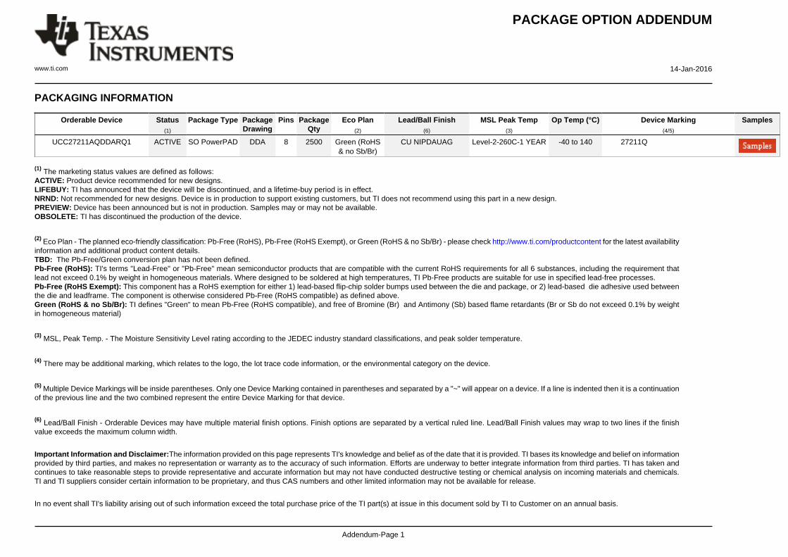
PACKAGING INFORMATION
Orderable Device Status(1)
Package Type PackageDrawing
Pins PackageQty
Eco Plan(2)
Lead/Ball Finish(6)
MSL Peak Temp(3)
Op Temp (°C) Device Marking(4/5)
Samples
UCC27211AQDDARQ1 ACTIVE SO PowerPAD DDA 8 2500 Green (RoHS& no Sb/Br)
CU NIPDAUAG Level-2-260C-1 YEAR -40 to 140 27211Q
(1) The marketing status values are defined as follows:ACTIVE: Product device recommended for new designs.LIFEBUY: TI has announced that the device will be discontinued, and a lifetime-buy period is in effect.NRND: Not recommended for new designs. Device is in production to support existing customers, but TI does not recommend using this part in a new design.PREVIEW: Device has been announced but is not in production. Samples may or may not be available.OBSOLETE: TI has discontinued the production of the device.
(2) Eco Plan - The planned eco-friendly classification: Pb-Free (RoHS), Pb-Free (RoHS Exempt), or Green (RoHS & no Sb/Br) - please check http://www.ti.com/productcontent for the latest availabilityinformation and additional product content details.TBD: The Pb-Free/Green conversion plan has not been defined.Pb-Free (RoHS): TI's terms "Lead-Free" or "Pb-Free" mean semiconductor products that are compatible with the current RoHS requirements for all 6 substances, including the requirement thatlead not exceed 0.1% by weight in homogeneous materials. Where designed to be soldered at high temperatures, TI Pb-Free products are suitable for use in specified lead-free processes.Pb-Free (RoHS Exempt): This component has a RoHS exemption for either 1) lead-based flip-chip solder bumps used between the die and package, or 2) lead-based die adhesive used betweenthe die and leadframe. The component is otherwise considered Pb-Free (RoHS compatible) as defined above.Green (RoHS & no Sb/Br): TI defines "Green" to mean Pb-Free (RoHS compatible), and free of Bromine (Br) and Antimony (Sb) based flame retardants (Br or Sb do not exceed 0.1% by weightin homogeneous material)
(3) MSL, Peak Temp. - The Moisture Sensitivity Level rating according to the JEDEC industry standard classifications, and peak solder temperature.
(4) There may be additional marking, which relates to the logo, the lot trace code information, or the environmental category on the device.
(5) Multiple Device Markings will be inside parentheses. Only one Device Marking contained in parentheses and separated by a "~" will appear on a device. If a line is indented then it is a continuationof the previous line and the two combined represent the entire Device Marking for that device.
(6) Lead/Ball Finish - Orderable Devices may have multiple material finish options. Finish options are separated by a vertical ruled line. Lead/Ball Finish values may wrap to two lines if the finishvalue exceeds the maximum column width.
Important Information and Disclaimer:The information provided on this page represents TI's knowledge and belief as of the date that it is provided. TI bases its knowledge and belief on informationprovided by third parties, and makes no representation or warranty as to the accuracy of such information. Efforts are underway to better integrate information from third parties. TI has taken andcontinues to take reasonable steps to provide representative and accurate information but may not have conducted destructive testing or chemical analysis on incoming materials and chemicals.TI and TI suppliers consider certain information to be proprietary, and thus CAS numbers and other limited information may not be available for release.
In no event shall TI's liability arising out of such information exceed the total purchase price of the TI part(s) at issue in this document sold by TI to Customer on an annual basis.
PACKAGE OPTION ADDENDUM
www.ti.com 14-Jan-2016
Addendum-Page 2
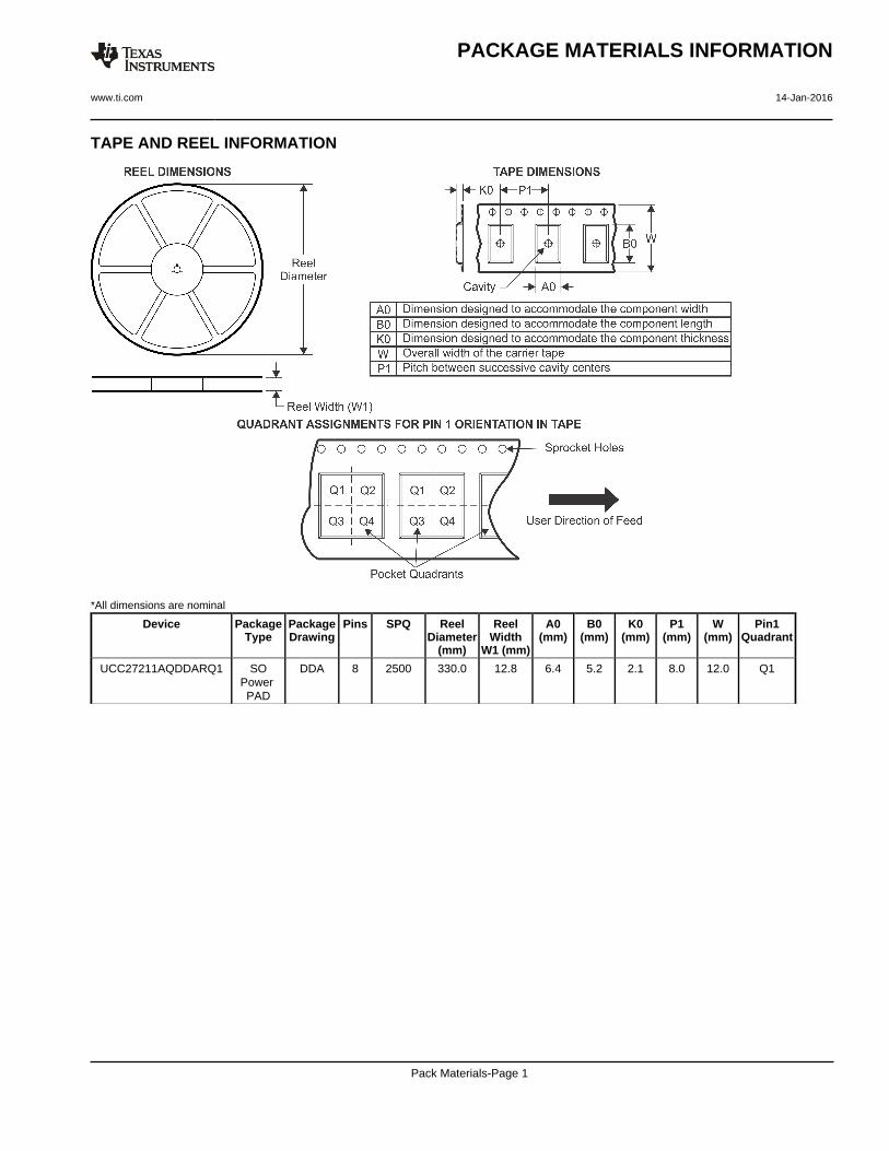
TAPE AND REEL INFORMATION
*All dimensions are nominal
Device PackageType
PackageDrawing
Pins SPQ ReelDiameter
(mm)
ReelWidth
W1 (mm)
A0(mm)
B0(mm)
K0(mm)
P1(mm)
W(mm)
Pin1Quadrant
UCC27211AQDDARQ1 SOPower PAD
DDA 8 2500 330.0 12.8 6.4 5.2 2.1 8.0 12.0 Q1
PACKAGE MATERIALS INFORMATION
www.ti.com 14-Jan-2016
Pack Materials-Page 1
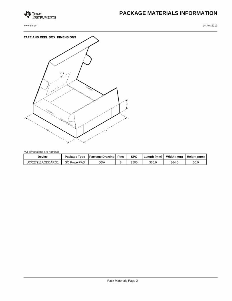
*All dimensions are nominal
Device Package Type Package Drawing Pins SPQ Length (mm) Width (mm) Height (mm)
UCC27211AQDDARQ1 SO PowerPAD DDA 8 2500 366.0 364.0 50.0
PACKAGE MATERIALS INFORMATION
www.ti.com 14-Jan-2016
Pack Materials-Page 2
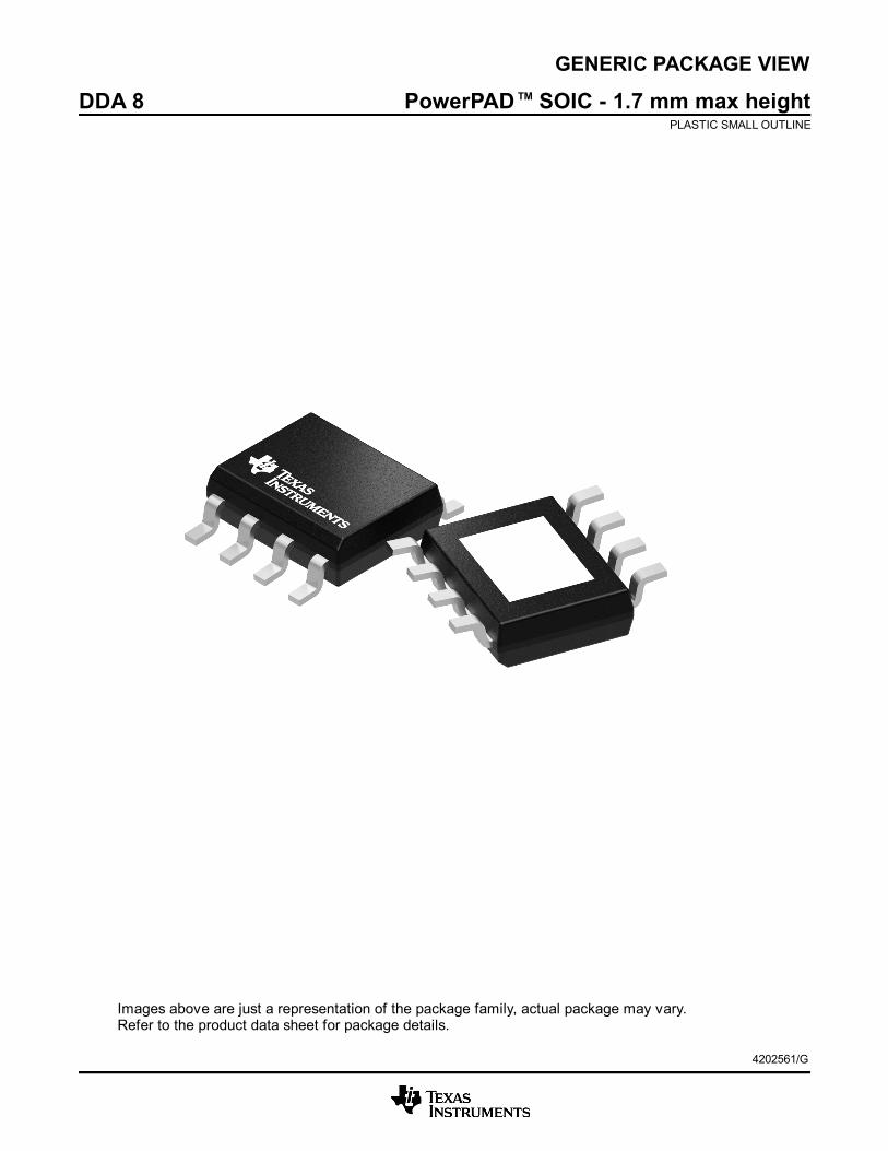
GENERIC PACKAGE VIEW
Images above are just a representation of the package family, actual package may vary.Refer to the product data sheet for package details.
DDA 8 PowerPAD TM SOIC - 1.7 mm max heightPLASTIC SMALL OUTLINE
4202561/G
IMPORTANT NOTICE
Texas Instruments Incorporated (TI) reserves the right to make corrections, enhancements, improvements and other changes to itssemiconductor products and services per JESD46, latest issue, and to discontinue any product or service per JESD48, latest issue. Buyersshould obtain the latest relevant information before placing orders and should verify that such information is current and complete.TI’s published terms of sale for semiconductor products (http://www.ti.com/sc/docs/stdterms.htm) apply to the sale of packaged integratedcircuit products that TI has qualified and released to market. Additional terms may apply to the use or sale of other types of TI products andservices.Reproduction of significant portions of TI information in TI data sheets is permissible only if reproduction is without alteration and isaccompanied by all associated warranties, conditions, limitations, and notices. TI is not responsible or liable for such reproduceddocumentation. Information of third parties may be subject to additional restrictions. Resale of TI products or services with statementsdifferent from or beyond the parameters stated by TI for that product or service voids all express and any implied warranties for theassociated TI product or service and is an unfair and deceptive business practice. TI is not responsible or liable for any such statements.Buyers and others who are developing systems that incorporate TI products (collectively, “Designers”) understand and agree that Designersremain responsible for using their independent analysis, evaluation and judgment in designing their applications and that Designers havefull and exclusive responsibility to assure the safety of Designers' applications and compliance of their applications (and of all TI productsused in or for Designers’ applications) with all applicable regulations, laws and other applicable requirements. Designer represents that, withrespect to their applications, Designer has all the necessary expertise to create and implement safeguards that (1) anticipate dangerousconsequences of failures, (2) monitor failures and their consequences, and (3) lessen the likelihood of failures that might cause harm andtake appropriate actions. Designer agrees that prior to using or distributing any applications that include TI products, Designer willthoroughly test such applications and the functionality of such TI products as used in such applications.TI’s provision of technical, application or other design advice, quality characterization, reliability data or other services or information,including, but not limited to, reference designs and materials relating to evaluation modules, (collectively, “TI Resources”) are intended toassist designers who are developing applications that incorporate TI products; by downloading, accessing or using TI Resources in anyway, Designer (individually or, if Designer is acting on behalf of a company, Designer’s company) agrees to use any particular TI Resourcesolely for this purpose and subject to the terms of this Notice.TI’s provision of TI Resources does not expand or otherwise alter TI’s applicable published warranties or warranty disclaimers for TIproducts, and no additional obligations or liabilities arise from TI providing such TI Resources. TI reserves the right to make corrections,enhancements, improvements and other changes to its TI Resources. TI has not conducted any testing other than that specificallydescribed in the published documentation for a particular TI Resource.Designer is authorized to use, copy and modify any individual TI Resource only in connection with the development of applications thatinclude the TI product(s) identified in such TI Resource. NO OTHER LICENSE, EXPRESS OR IMPLIED, BY ESTOPPEL OR OTHERWISETO ANY OTHER TI INTELLECTUAL PROPERTY RIGHT, AND NO LICENSE TO ANY TECHNOLOGY OR INTELLECTUAL PROPERTYRIGHT OF TI OR ANY THIRD PARTY IS GRANTED HEREIN, including but not limited to any patent right, copyright, mask work right, orother intellectual property right relating to any combination, machine, or process in which TI products or services are used. Informationregarding or referencing third-party products or services does not constitute a license to use such products or services, or a warranty orendorsement thereof. Use of TI Resources may require a license from a third party under the patents or other intellectual property of thethird party, or a license from TI under the patents or other intellectual property of TI.TI RESOURCES ARE PROVIDED “AS IS” AND WITH ALL FAULTS. TI DISCLAIMS ALL OTHER WARRANTIES ORREPRESENTATIONS, EXPRESS OR IMPLIED, REGARDING RESOURCES OR USE THEREOF, INCLUDING BUT NOT LIMITED TOACCURACY OR COMPLETENESS, TITLE, ANY EPIDEMIC FAILURE WARRANTY AND ANY IMPLIED WARRANTIES OFMERCHANTABILITY, FITNESS FOR A PARTICULAR PURPOSE, AND NON-INFRINGEMENT OF ANY THIRD PARTY INTELLECTUALPROPERTY RIGHTS. TI SHALL NOT BE LIABLE FOR AND SHALL NOT DEFEND OR INDEMNIFY DESIGNER AGAINST ANY CLAIM,INCLUDING BUT NOT LIMITED TO ANY INFRINGEMENT CLAIM THAT RELATES TO OR IS BASED ON ANY COMBINATION OFPRODUCTS EVEN IF DESCRIBED IN TI RESOURCES OR OTHERWISE. IN NO EVENT SHALL TI BE LIABLE FOR ANY ACTUAL,DIRECT, SPECIAL, COLLATERAL, INDIRECT, PUNITIVE, INCIDENTAL, CONSEQUENTIAL OR EXEMPLARY DAMAGES INCONNECTION WITH OR ARISING OUT OF TI RESOURCES OR USE THEREOF, AND REGARDLESS OF WHETHER TI HAS BEENADVISED OF THE POSSIBILITY OF SUCH DAMAGES.Unless TI has explicitly designated an individual product as meeting the requirements of a particular industry standard (e.g., ISO/TS 16949and ISO 26262), TI is not responsible for any failure to meet such industry standard requirements.Where TI specifically promotes products as facilitating functional safety or as compliant with industry functional safety standards, suchproducts are intended to help enable customers to design and create their own applications that meet applicable functional safety standardsand requirements. Using products in an application does not by itself establish any safety features in the application. Designers mustensure compliance with safety-related requirements and standards applicable to their applications. Designer may not use any TI products inlife-critical medical equipment unless authorized officers of the parties have executed a special contract specifically governing such use.Life-critical medical equipment is medical equipment where failure of such equipment would cause serious bodily injury or death (e.g., lifesupport, pacemakers, defibrillators, heart pumps, neurostimulators, and implantables). Such equipment includes, without limitation, allmedical devices identified by the U.S. Food and Drug Administration as Class III devices and equivalent classifications outside the U.S.TI may expressly designate certain products as completing a particular qualification (e.g., Q100, Military Grade, or Enhanced Product).Designers agree that it has the necessary expertise to select the product with the appropriate qualification designation for their applicationsand that proper product selection is at Designers’ own risk. Designers are solely responsible for compliance with all legal and regulatoryrequirements in connection with such selection.Designer will fully indemnify TI and its representatives against any damages, costs, losses, and/or liabilities arising out of Designer’s non-compliance with the terms and provisions of this Notice.
Mailing Address: Texas Instruments, Post Office Box 655303, Dallas, Texas 75265Copyright © 2018, Texas Instruments Incorporated