Embed Size (px)
Citation preview
UFX6000
USB 2.0 Hi-Speed Graphics Controller with VGA, HDMI/DVI, and Digital RGB Interfaces
DatasheetPRODUCT FEATURES
Highlights Single-Chip Hi-Speed USB 2.0 Graphics Adapter
USB 2.0 Device Controller with Integrated USB 2.0 PHY
Highly Efficient Compression Algorithm
HDMI/DVI Display Connectivity via Integrated HDMI/DVI Controller/PHY
VGA Display Connectivity via Integrated Video DAC
Support for External Display Interface IC’s via Digital RGB Interface
High Performance DDR2 SDRAM Controller with Integrated DDR2 PHY
Target Applications USB to Video Adapters
Docking Stations, USB Port Replicators
Thin Clients
USB Monitors and Projectors
Embedded Systems
Features USB 2.0 Device Controller
— Fully compliant with Universal Serial Bus Specification Revision 2.0
— Operates in HS (480 Mbps) mode— Supports Control, Bulk-Out, and Interrupt-In endpoints— Supports vendor specific commands— Integrated USB 2.0 PHY— Integrated USB termination pull-up/pull-down resistors— Short circuit protection of USB differential signals
Graphics Subsystem— Integrated HDMI/DVI Controller and PHY
– Complies with DVI specification v1.0 – Complies with HDMI specification v1.3– S/PDIF and I2S inputs for HDMI audio
(2-channel uncompressed PCM)– Master I2C interface for DDC connection
— Integrated Triple 10-bit Video DAC with VGA output— Digital RGB Interface
– 12/15-bit double data rate digital RGB– 24-bit single data rate digital RGB
— Supports up to 2048x1152 (QWXGA) with 32-bit color— 8-bit and 16-bit color support— Supports display cloning and extending— Standard and wide screen aspect ratios— Complies with VESA auto display identification— Gamma correction— Color Look-Up Table (CLUT)— Triple-buffered animations— Graphics Engine
– Optimized algorithms for static and dynamic content– I2C controller
DDR2 SDRAM Controller— 16-bit data bus, 13-bit address bus— JEDEC DDR2 compliant (JESD79-2E)— Integrated DDR2 SDRAM PHY
Power— Reduced power operating modes— Supports bus-powered and self-powered operation
Miscellaneous Features— Optional EEPROM controller— IEEE 1149.1 (JTAG) boundary scan TAP controller
Software— Microsoft Windows® XP/Vista/7 drivers
Packaging & Environmental— 225-ball LFBGA, RoHS compliant package— Commercial temperature range (0°C to +70°C)
SMSC UFX6000 Revision 1.4 (06-24-13)DATASHEET
USB 2.0 Hi-Speed Graphics Controller with VGA, HDMI/DVI, and Digital RGB Interfaces
Datasheet
Order Number:
UFX6000-VE for 225-Ball LFBGA RoHS Compliant Package (0 TO +70°C Temp Range)
This product meets the halogen maximum concentration values per IEC61249-2-21
For RoHS compliance and environmental information, please visit www.smsc.com/rohs
Please contact your SMSC sales representative for additional documentation related to this product such as application notes, anomaly sheets, and design guidelines.
Copyright © 2013 SMSC or its subsidiaries. All rights reserved.
Circuit diagrams and other information relating to SMSC products are included as a means of illustrating typical applications. Consequently, complete information sufficient forconstruction purposes is not necessarily given. Although the information has been checked and is believed to be accurate, no responsibility is assumed for inaccuracies. SMSCreserves the right to make changes to specifications and product descriptions at any time without notice. Contact your local SMSC sales office to obtain the latest specificationsbefore placing your product order. The provision of this information does not convey to the purchaser of the described semiconductor devices any licenses under any patentrights or other intellectual property rights of SMSC or others. All sales are expressly conditional on your agreement to the terms and conditions of the most recently datedversion of SMSC's standard Terms of Sale Agreement dated before the date of your order (the "Terms of Sale Agreement"). The product may contain design defects or errorsknown as anomalies which may cause the product's functions to deviate from published specifications. Anomaly sheets are available upon request. SMSC products are notdesigned, intended, authorized or warranted for use in any life support or other application where product failure could cause or contribute to personal injury or severe propertydamage. Any and all such uses without prior written approval of an Officer of SMSC and further testing and/or modification will be fully at the risk of the customer. Copies ofthis document or other SMSC literature, as well as the Terms of Sale Agreement, may be obtained by visiting SMSC’s website at http://www.smsc.com. SMSC is a registeredtrademark of Standard Microsystems Corporation (“SMSC”). Product names and company names are the trademarks of their respective holders.
The MIcrochip name and logo, and the Microchip logo are registered trademarks of MIcrochip Technology Incorporated in the U.S.A. and other countries.
SMSC DISCLAIMS AND EXCLUDES ANY AND ALL WARRANTIES, INCLUDING WITHOUT LIMITATION ANY AND ALL IMPLIED WARRANTIES OF MERCHANTABILITY,FITNESS FOR A PARTICULAR PURPOSE, TITLE, AND AGAINST INFRINGEMENT AND THE LIKE, AND ANY AND ALL WARRANTIES ARISING FROM ANY COURSEOF DEALING OR USAGE OF TRADE. IN NO EVENT SHALL SMSC BE LIABLE FOR ANY DIRECT, INCIDENTAL, INDIRECT, SPECIAL, PUNITIVE, OR CONSEQUENTIALDAMAGES; OR FOR LOST DATA, PROFITS, SAVINGS OR REVENUES OF ANY KIND; REGARDLESS OF THE FORM OF ACTION, WHETHER BASED ON CONTRACT;TORT; NEGLIGENCE OF SMSC OR OTHERS; STRICT LIABILITY; BREACH OF WARRANTY; OR OTHERWISE; WHETHER OR NOT ANY REMEDY OF BUYER IS HELDTO HAVE FAILED OF ITS ESSENTIAL PURPOSE, AND WHETHER OR NOT SMSC HAS BEEN ADVISED OF THE POSSIBILITY OF SUCH DAMAGES.
Revision 1.4 (06-24-13) 2 SMSC UFX6000DATASHEET
USB 2.0 Hi-Speed Graphics Controller with VGA, HDMI/DVI, and Digital RGB Interfaces
Datasheet
SMSC UFX6000 3 Revision 1.4 (06-24-13)DATASHEET
Table of Contents
Chapter 1 Introduction . . . . . . . . . . . . . . . . . . . . . . . . . . . . . . . . . . . . . . . . . . . . . . . . . . . . . . . . 61.1 USB Device Controller . . . . . . . . . . . . . . . . . . . . . . . . . . . . . . . . . . . . . . . . . . . . . . . . . . . . . . . . . . . 61.2 Graphics Subsystem. . . . . . . . . . . . . . . . . . . . . . . . . . . . . . . . . . . . . . . . . . . . . . . . . . . . . . . . . . . . . 71.3 DDR2 SDRAM Interface . . . . . . . . . . . . . . . . . . . . . . . . . . . . . . . . . . . . . . . . . . . . . . . . . . . . . . . . . . 71.4 Peripherals . . . . . . . . . . . . . . . . . . . . . . . . . . . . . . . . . . . . . . . . . . . . . . . . . . . . . . . . . . . . . . . . . . . . 7
Chapter 2 Pin Description and Configuration . . . . . . . . . . . . . . . . . . . . . . . . . . . . . . . . . . . . . . 82.1 Pin Assignments . . . . . . . . . . . . . . . . . . . . . . . . . . . . . . . . . . . . . . . . . . . . . . . . . . . . . . . . . . . . . . . 252.2 Buffer Types . . . . . . . . . . . . . . . . . . . . . . . . . . . . . . . . . . . . . . . . . . . . . . . . . . . . . . . . . . . . . . . . . . 28
Chapter 3 Power Connections . . . . . . . . . . . . . . . . . . . . . . . . . . . . . . . . . . . . . . . . . . . . . . . . . . 29
Chapter 4 EEPROM. . . . . . . . . . . . . . . . . . . . . . . . . . . . . . . . . . . . . . . . . . . . . . . . . . . . . . . . . . 304.1 EEPROM Format . . . . . . . . . . . . . . . . . . . . . . . . . . . . . . . . . . . . . . . . . . . . . . . . . . . . . . . . . . . . . . 304.2 EEPROM Defaults . . . . . . . . . . . . . . . . . . . . . . . . . . . . . . . . . . . . . . . . . . . . . . . . . . . . . . . . . . . . . 354.3 EEPROM Auto-Load. . . . . . . . . . . . . . . . . . . . . . . . . . . . . . . . . . . . . . . . . . . . . . . . . . . . . . . . . . . . 354.4 Customized Operation Without EEPROM . . . . . . . . . . . . . . . . . . . . . . . . . . . . . . . . . . . . . . . . . . . 35
Chapter 5 Operational Characteristics. . . . . . . . . . . . . . . . . . . . . . . . . . . . . . . . . . . . . . . . . . . 365.1 Absolute Maximum Ratings*. . . . . . . . . . . . . . . . . . . . . . . . . . . . . . . . . . . . . . . . . . . . . . . . . . . . . . 365.2 Operating Conditions** . . . . . . . . . . . . . . . . . . . . . . . . . . . . . . . . . . . . . . . . . . . . . . . . . . . . . . . . . . 365.3 Package Thermal Specifications . . . . . . . . . . . . . . . . . . . . . . . . . . . . . . . . . . . . . . . . . . . . . . . . . . 375.4 Current Consumption . . . . . . . . . . . . . . . . . . . . . . . . . . . . . . . . . . . . . . . . . . . . . . . . . . . . . . . . . . . 37
5.4.1 SUSPEND Power State. . . . . . . . . . . . . . . . . . . . . . . . . . . . . . . . . . . . . . . . . . . . . . . . . . 375.4.2 Operational . . . . . . . . . . . . . . . . . . . . . . . . . . . . . . . . . . . . . . . . . . . . . . . . . . . . . . . . . . . 38
5.5 DC Specifications . . . . . . . . . . . . . . . . . . . . . . . . . . . . . . . . . . . . . . . . . . . . . . . . . . . . . . . . . . . . . . 395.6 AC Specifications . . . . . . . . . . . . . . . . . . . . . . . . . . . . . . . . . . . . . . . . . . . . . . . . . . . . . . . . . . . . . . 40
5.6.1 Power Sequence Timing . . . . . . . . . . . . . . . . . . . . . . . . . . . . . . . . . . . . . . . . . . . . . . . . . 415.6.2 Power-On Reset Timing . . . . . . . . . . . . . . . . . . . . . . . . . . . . . . . . . . . . . . . . . . . . . . . . . 425.6.3 Reset Timing . . . . . . . . . . . . . . . . . . . . . . . . . . . . . . . . . . . . . . . . . . . . . . . . . . . . . . . . . . 435.6.4 Video DAC Timing . . . . . . . . . . . . . . . . . . . . . . . . . . . . . . . . . . . . . . . . . . . . . . . . . . . . . . 435.6.5 Digital RGB Timing . . . . . . . . . . . . . . . . . . . . . . . . . . . . . . . . . . . . . . . . . . . . . . . . . . . . . 445.6.6 EEPROM Timing . . . . . . . . . . . . . . . . . . . . . . . . . . . . . . . . . . . . . . . . . . . . . . . . . . . . . . . 465.6.7 JTAG Timing . . . . . . . . . . . . . . . . . . . . . . . . . . . . . . . . . . . . . . . . . . . . . . . . . . . . . . . . . . 47
5.7 Clock Circuit . . . . . . . . . . . . . . . . . . . . . . . . . . . . . . . . . . . . . . . . . . . . . . . . . . . . . . . . . . . . . . . . . . 48
Chapter 6 Package Outline . . . . . . . . . . . . . . . . . . . . . . . . . . . . . . . . . . . . . . . . . . . . . . . . . . . . 496.1 225-LFBGA Package . . . . . . . . . . . . . . . . . . . . . . . . . . . . . . . . . . . . . . . . . . . . . . . . . . . . . . . . . . . 49
Chapter 7 Datasheet Revision History . . . . . . . . . . . . . . . . . . . . . . . . . . . . . . . . . . . . . . . . . . . 51
USB 2.0 Hi-Speed Graphics Controller with VGA, HDMI/DVI, and Digital RGB Interfaces
Datasheet
Revision 1.4 (06-24-13) 4 SMSC UFX6000DATASHEET
List of Figures
Figure 1.1 Internal Block Diagram. . . . . . . . . . . . . . . . . . . . . . . . . . . . . . . . . . . . . . . . . . . . . . . . . . . . . . . 6Figure 2.1 Pin Assignments (TOP VIEW) . . . . . . . . . . . . . . . . . . . . . . . . . . . . . . . . . . . . . . . . . . . . . . . . . 8Figure 3.1 Power Connections . . . . . . . . . . . . . . . . . . . . . . . . . . . . . . . . . . . . . . . . . . . . . . . . . . . . . . . . 29Figure 5.1 Power-On Timing . . . . . . . . . . . . . . . . . . . . . . . . . . . . . . . . . . . . . . . . . . . . . . . . . . . . . . . . . . 41Figure 5.1 nRESET Power-On Timing . . . . . . . . . . . . . . . . . . . . . . . . . . . . . . . . . . . . . . . . . . . . . . . . . . 42Figure 5.1 nRESET Timing . . . . . . . . . . . . . . . . . . . . . . . . . . . . . . . . . . . . . . . . . . . . . . . . . . . . . . . . . . . 43Figure 5.2 Digital RGB Timing - DDR Mode . . . . . . . . . . . . . . . . . . . . . . . . . . . . . . . . . . . . . . . . . . . . . . 44Figure 5.3 Digital RGB Timing - SDR Mode . . . . . . . . . . . . . . . . . . . . . . . . . . . . . . . . . . . . . . . . . . . . . . 45Figure 5.4 EEPROM Timing . . . . . . . . . . . . . . . . . . . . . . . . . . . . . . . . . . . . . . . . . . . . . . . . . . . . . . . . . . 46Figure 5.5 JTAG Timing . . . . . . . . . . . . . . . . . . . . . . . . . . . . . . . . . . . . . . . . . . . . . . . . . . . . . . . . . . . . . 47Figure 6.1 225-LFBGA Package Definition . . . . . . . . . . . . . . . . . . . . . . . . . . . . . . . . . . . . . . . . . . . . . . . 49Figure 6.2 225-LFBGA Package Ball Detail . . . . . . . . . . . . . . . . . . . . . . . . . . . . . . . . . . . . . . . . . . . . . . 49Figure 6.1 225-LFBGA Recommended PCB Land Pattern. . . . . . . . . . . . . . . . . . . . . . . . . . . . . . . . . . . 50
USB 2.0 Hi-Speed Graphics Controller with VGA, HDMI/DVI, and Digital RGB Interfaces
Datasheet
SMSC UFX6000 5 Revision 1.4 (06-24-13)DATASHEET
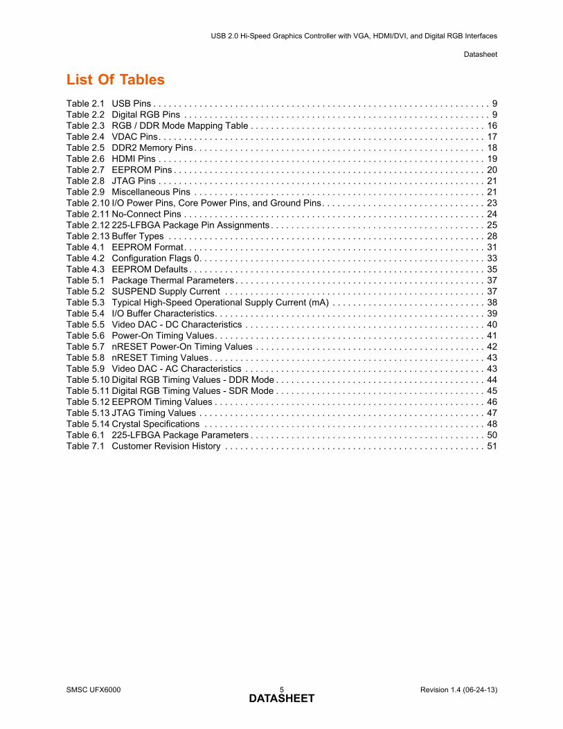
List Of Tables
Table 2.1 USB Pins . . . . . . . . . . . . . . . . . . . . . . . . . . . . . . . . . . . . . . . . . . . . . . . . . . . . . . . . . . . . . . . . . . 9Table 2.2 Digital RGB Pins . . . . . . . . . . . . . . . . . . . . . . . . . . . . . . . . . . . . . . . . . . . . . . . . . . . . . . . . . . . . 9Table 2.3 RGB / DDR Mode Mapping Table . . . . . . . . . . . . . . . . . . . . . . . . . . . . . . . . . . . . . . . . . . . . . . 16Table 2.4 VDAC Pins. . . . . . . . . . . . . . . . . . . . . . . . . . . . . . . . . . . . . . . . . . . . . . . . . . . . . . . . . . . . . . . . 17Table 2.5 DDR2 Memory Pins . . . . . . . . . . . . . . . . . . . . . . . . . . . . . . . . . . . . . . . . . . . . . . . . . . . . . . . . . 18Table 2.6 HDMI Pins . . . . . . . . . . . . . . . . . . . . . . . . . . . . . . . . . . . . . . . . . . . . . . . . . . . . . . . . . . . . . . . . 19Table 2.7 EEPROM Pins . . . . . . . . . . . . . . . . . . . . . . . . . . . . . . . . . . . . . . . . . . . . . . . . . . . . . . . . . . . . . 20Table 2.8 JTAG Pins . . . . . . . . . . . . . . . . . . . . . . . . . . . . . . . . . . . . . . . . . . . . . . . . . . . . . . . . . . . . . . . . 21Table 2.9 Miscellaneous Pins . . . . . . . . . . . . . . . . . . . . . . . . . . . . . . . . . . . . . . . . . . . . . . . . . . . . . . . . . 21Table 2.10 I/O Power Pins, Core Power Pins, and Ground Pins. . . . . . . . . . . . . . . . . . . . . . . . . . . . . . . . 23Table 2.11 No-Connect Pins . . . . . . . . . . . . . . . . . . . . . . . . . . . . . . . . . . . . . . . . . . . . . . . . . . . . . . . . . . . 24Table 2.12 225-LFBGA Package Pin Assignments . . . . . . . . . . . . . . . . . . . . . . . . . . . . . . . . . . . . . . . . . . 25Table 2.13 Buffer Types . . . . . . . . . . . . . . . . . . . . . . . . . . . . . . . . . . . . . . . . . . . . . . . . . . . . . . . . . . . . . . 28Table 4.1 EEPROM Format. . . . . . . . . . . . . . . . . . . . . . . . . . . . . . . . . . . . . . . . . . . . . . . . . . . . . . . . . . . 31Table 4.2 Configuration Flags 0. . . . . . . . . . . . . . . . . . . . . . . . . . . . . . . . . . . . . . . . . . . . . . . . . . . . . . . . 33Table 4.3 EEPROM Defaults . . . . . . . . . . . . . . . . . . . . . . . . . . . . . . . . . . . . . . . . . . . . . . . . . . . . . . . . . . 35Table 5.1 Package Thermal Parameters . . . . . . . . . . . . . . . . . . . . . . . . . . . . . . . . . . . . . . . . . . . . . . . . . 37Table 5.2 SUSPEND Supply Current . . . . . . . . . . . . . . . . . . . . . . . . . . . . . . . . . . . . . . . . . . . . . . . . . . . 37Table 5.3 Typical High-Speed Operational Supply Current (mA) . . . . . . . . . . . . . . . . . . . . . . . . . . . . . . 38Table 5.4 I/O Buffer Characteristics. . . . . . . . . . . . . . . . . . . . . . . . . . . . . . . . . . . . . . . . . . . . . . . . . . . . . 39Table 5.5 Video DAC - DC Characteristics . . . . . . . . . . . . . . . . . . . . . . . . . . . . . . . . . . . . . . . . . . . . . . . 40Table 5.6 Power-On Timing Values. . . . . . . . . . . . . . . . . . . . . . . . . . . . . . . . . . . . . . . . . . . . . . . . . . . . . 41Table 5.7 nRESET Power-On Timing Values . . . . . . . . . . . . . . . . . . . . . . . . . . . . . . . . . . . . . . . . . . . . . 42Table 5.8 nRESET Timing Values . . . . . . . . . . . . . . . . . . . . . . . . . . . . . . . . . . . . . . . . . . . . . . . . . . . . . . 43Table 5.9 Video DAC - AC Characteristics . . . . . . . . . . . . . . . . . . . . . . . . . . . . . . . . . . . . . . . . . . . . . . . 43Table 5.10 Digital RGB Timing Values - DDR Mode . . . . . . . . . . . . . . . . . . . . . . . . . . . . . . . . . . . . . . . . . 44Table 5.11 Digital RGB Timing Values - SDR Mode . . . . . . . . . . . . . . . . . . . . . . . . . . . . . . . . . . . . . . . . . 45Table 5.12 EEPROM Timing Values . . . . . . . . . . . . . . . . . . . . . . . . . . . . . . . . . . . . . . . . . . . . . . . . . . . . . 46Table 5.13 JTAG Timing Values . . . . . . . . . . . . . . . . . . . . . . . . . . . . . . . . . . . . . . . . . . . . . . . . . . . . . . . . 47Table 5.14 Crystal Specifications . . . . . . . . . . . . . . . . . . . . . . . . . . . . . . . . . . . . . . . . . . . . . . . . . . . . . . . 48Table 6.1 225-LFBGA Package Parameters . . . . . . . . . . . . . . . . . . . . . . . . . . . . . . . . . . . . . . . . . . . . . . 50Table 7.1 Customer Revision History . . . . . . . . . . . . . . . . . . . . . . . . . . . . . . . . . . . . . . . . . . . . . . . . . . . 51
USB 2.0 Hi-Speed Graphics Controller with VGA, HDMI/DVI, and Digital RGB Interfaces
Datasheet
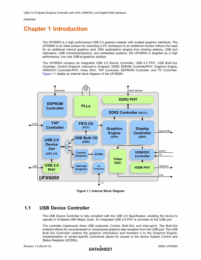
Chapter 1 Introduction
The UFX6000 is a high performance USB 2.0 graphics adapter with multiple graphics interfaces. TheUFX6000 is an ideal solution for extending a PC workspace to an additional monitor without the needfor an additional internal graphics card. With applications ranging from docking stations, USB portreplicators, USB monitors/projectors, and embedded systems, the UFX6000 is targeted as a highperformance, low cost USB-to-graphics solution.
The UFX6000 contains an integrated USB 2.0 Device Controller, USB 2.0 PHY, USB Bulk-OutController, Control Endpoint, Interrupt-In Endpoint, DDR2 SDRAM Controller/PHY, Graphics Engine,HDMI/DVI Controller/PHY, Video DAC, TAP Controller, EEPROM Controller, and I2C Controller.Figure 1.1 details an internal block diagram of the UFX6000.
1.1 USB Device Controller
The USB Device Controller is fully compliant with the USB 2.0 Specification, enabling the device tooperate in Hi-Speed (480 Mbps) mode. An integrated USB 2.0 PHY is provided on the USB port.
The controller implements three USB endpoints: Control, Bulk-Out, and Interrupt-In. The Bulk-Outendpoint allows for uncompressed or compressed graphics data reception from the USB port. The USBBulk-Out Controller collects the graphics information and transfers it to the Graphics Engine.Implementation of vendor-specific commands allows for access to the device System Control andStatus Registers (SCSRs).
Figure 1.1 Internal Block Diagram
UFX6000
DDR2 PHY
DDR2 Controller (DCTL)
USB Bulk Ctl(URX)
EEPROMController
PLLs
EEPROM DDR2 SDRAM
Graphics Engine
(GPH)
Control Endpoint
SCSRs
HDMI/DVI
Video DAC
HDMI PHY
HDMI/DVIController
VGA
MU
X
Digital RGB
I2C Controller
I2C
FIFO Ctl(FCT)
USB 2.0 Device
Ctrl(UDC 2.0)
Display Controller
(DISP)
Interrupt Endpoint
USB 2.0 PHY
USB
TAP Controller
JTAG
S/PDIF
I2S
Revision 1.4 (06-24-13) 6 SMSC UFX6000DATASHEET
USB 2.0 Hi-Speed Graphics Controller with VGA, HDMI/DVI, and Digital RGB Interfaces
Datasheet
1.2 Graphics Subsystem
The Graphics Subsystem consists of the following main blocks: the Graphics Engine, DisplayController, HDMI/DVI Controller/PHY, Video DAC, and the Digital RGB Interface. Together, theseblocks support high definition resolutions of up to 2048x1152 (QWXGA) with 32-bit true color in bothstandard and wide screen aspect ratios. The HDMI/DVI interface is compliant with the HDMI v1.3 andDVI v1.0 specifications and supports 2-channel uncompressed PCM audio via a S/PDIF or I2S input.The Display Controller also supports 8-bit and 16-bit color, gamma correction, Color Look-Up Table(CLUT) and triple-buffered animations. The DDC2B/EDID VESA standard is supported, allowing thehost OS and device drivers to query the monitor’s frequency, resolution, and other features for trueplug-and-play and intelligent mode setting capabilities.
Once the graphics data has been received via the USB Bulk-Out Controller, it is sent to the GraphicsEngine. If the data is compressed, the Graphics Engine decompresses it via algorithms that have beenoptimized for speed and quality. The device’s decompression algorithms have been designed to workseamlessly with the compression algorithms utilized in the software device drivers.
The graphics data is then transferred to the SDRAM via the DDR2 SDRAM Controller. The DisplayController generates all display and interface timing signals, retrieves the graphics data from the DDR2SDRAM, and sends it to the HDMI/DVI Controller/PHY, Video DAC, or Digital RGB Interface.
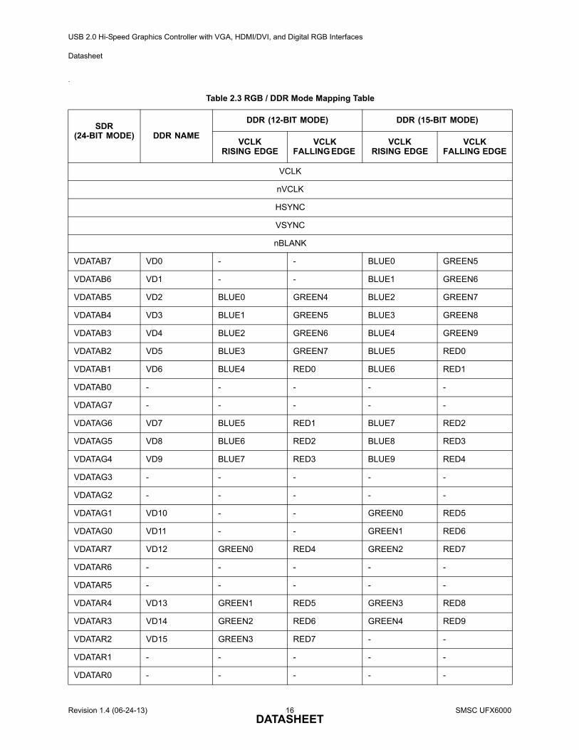
The Digital RGB Interface may be used to connect external display interface IC’s (e.g., DisplayPort,etc.) via the provided RGB data channel busses and control signals. The Digital RGB Interfacesupports two modes of operation: 24-bit single data rate mode and 12/15-bit double data rate mode.24-bit mode is single edge triggered and utilizes the full 24-bit data bus width. The 12/15-bit mode istriggered on both clock edges and utilizes 12/15-bits of the data bus width.
1.3 DDR2 SDRAM Interface
The UFX6000 provides a full JEDEC compliant (JESD79-2E) DDR2 SDRAM Controller and PHY forinterfacing to external DDR2 SDRAM. The DDR2 SDRAM interface is comprised of JEDEC standard1.8V I/O signals grouped into control signals, a 16-bit data bus, and a 13-bit address bus.
The DDR2 SDRAM Controller transfers the graphics data in and out of external SDRAM through theDDR2 SDRAM PHY. External SDRAM is used as storage for the graphics and acts a a buffer betweenthe Graphics Engine and Display Controller.
1.4 Peripherals
The UFX6000 also contains an EEPROM Controller, I2C Controller, and TAP Controller.
The EEPROM Controller allows connection to an external EEPROM for automatic loading of staticconfiguration data upon power-on, pin reset, or software reset. The EEPROM can be configured toload USB descriptors and USB device configuration.
The integrated IEEE 1149.1 compliant TAP controller provides boundary scan via JTAG.
SMSC UFX6000 7 Revision 1.4 (06-24-13)DATASHEET
USB 2.0 Hi-Speed Graphics Controller with VGA, HDMI/DVI, and Digital RGB Interfaces
Datasheet
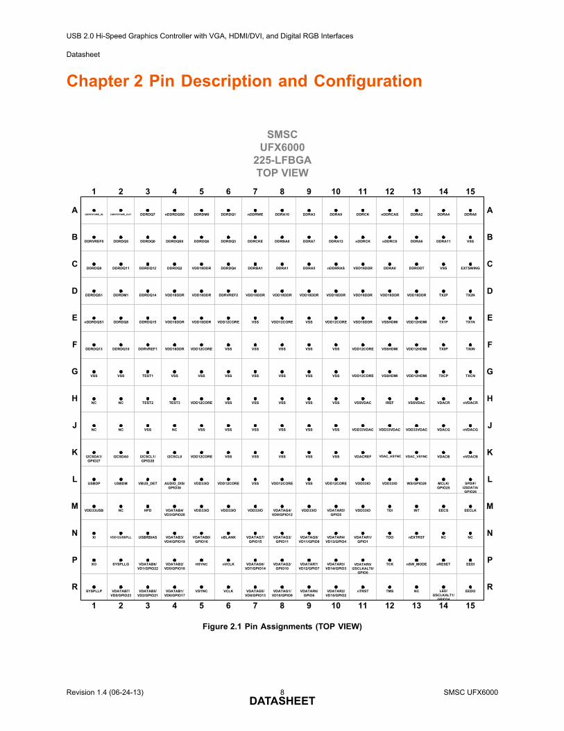
Chapter 2 Pin Description and Configuration
Figure 2.1 Pin Assignments (TOP VIEW)
nDDRDQS0
DDRDQ5 DDRDQ0
VDD18DDR
VDD18DDR
DDRDQ3
nDDRWE DDRA10 DDRA3 DDRA9 DDRCK nDDRCAS DDRA2
VDD18DDR
VSS
DDRFIFOWE_OUT DDRDQ7
DDRDQ12
DDRDQS0
DDRDM0
VDD18DDR
DDRDQ4
DDRCKE DDRBA0 DDRA7 DDRA12 nDDRCK nDDRCS DDRA6
DDRA4
TX2P
DDRVREF0
DDRDQ11DDRDQ9 DDRDQ2
DDRDQ6
DDRDQ1
DDRVREF2
DDRBA1 DDRA1 DDRA5 nDDRRAS VDD18DDR DDRA0 DDRODT
DDRA11
DDRA8
TX2NDDRDQS1 DDRDM1 DDRDQ14
DDRDQ8 DDRDQ15 VDD18DDR
DDRDQ10 DDRVREF1
nDDRDQS1 TX1N
VSS TEST1
DDRDQ13
VSSHDMI
NC TEST2
VSS
NC VSS
NC
I2CSDA0 I2CSCL1/GPIO28
NC
USBDM VBUS_DET
I2CSDA1/GPIO27
NC HPD
USBDP
USBRBIAS VDATAB3/VD4/GPIO19
VDD33USB
VDATAB2/VD5/GPIO18
XI VDD12USBPLL NC
SYSPLLG VDATAB6/VD1/GPIO22
VDATAB5/VD2/GPIO21
VDATAB1/VD6/GPIO17
XO
SYSPLLP VSYNC VDATAG5/VD8/GPIO13
VDATAG1/VD10/GPIO9
EEDI
VDATAB7/VD0/GPIO23
VCLK VDATAR6/GPIO6
VDATAB0/GPIO16
VDD18DDR
VSS
TEST3
NC
I2CSCL0
AUDIO_DIS/GPIO30
VDATAB4/VD3/GPIO20
VDD18DDR VDD18DDR VDD18DDR VDD18DDR VDD18DDR VDD18DDR
TX0N
TXCN
nVDACR
nVDACG
nVDACB
SPDIF/ I2SDATA/GPIO26
EECLK
DDRFIFOWE_IN
VSS
EXTSWING
EEDOVDATAR2/VD15/GPIO2
nTRST TMS NC LED/I2SCLKALT1/
GPIO24
TX1P
HSYNC
nBLANK
nVCLK VDATAG6/VD7/GPIO14
VDATAG2/GPIO10
VDATAR7/VD12/GPIO7
VDATAR3/VD14/GPIO3
VDATAR0/I2SCLKALT0/
GPIO0
TCK
VDD12CORE VSS VDD12CORE VSS VDD12CORE VDD18DDR VSSHDMI
nEXTRST
nSW_MODE nRESET
NC
EECS
MCLK/GPIO25
VDACB
VDACG
VDACR
TXCP
TX0PVDD12HDMI
VDD12HDMIVDD18DDR
VDD12CORE VSS
VSS
VDD12CORE
VSS
VDD12CORE
VDD33IO
VDD33IO
VDD12COREVSS
VSS
VSS
VDD33IO
VDATAG3/GPIO11
VDATAR1/GPIO1
WS/GPIO29
VDD33VDAC
VDD12HDMI
VSSHDMIVSSVSSVSS
VSS VSS VSS VSS VSS VDD12CORE
IREFVSS VSS VSS VSS VSSVDAC
VDD33VDACVSS VSS VSS VSS VDD33VDAC
VDAC_HSYNCVSS VSS VSS VSS VDACREF
VDD33IOVSS VDD12CORE VSS VDD12CORE VDD33IO
TDIVDD33IO VDATAG4/VD9/GPIO12
VDD33IO VDATAR5/GPIO5
VDD33IO
TDOVDATAG7/GPIO15
VDATAG0/VD11/GPIO8
VDATAR4/VD13/GPIO4
VSS
VDD12CORE
VSSVDAC
VDAC_VSYNC
INT
151413121110987654321
A
B
C
D
E
F
G
H
J
K
L
M
N
P
R
B
C
D
E
F
G
H
J
K
L
M
N
P
R
151413121110987654321
A
SMSCUFX6000
225-LFBGATOP VIEW
Revision 1.4 (06-24-13) 8 SMSC UFX6000DATASHEET
USB 2.0 Hi-Speed Graphics Controller with VGA, HDMI/DVI, and Digital RGB Interfaces
Datasheet
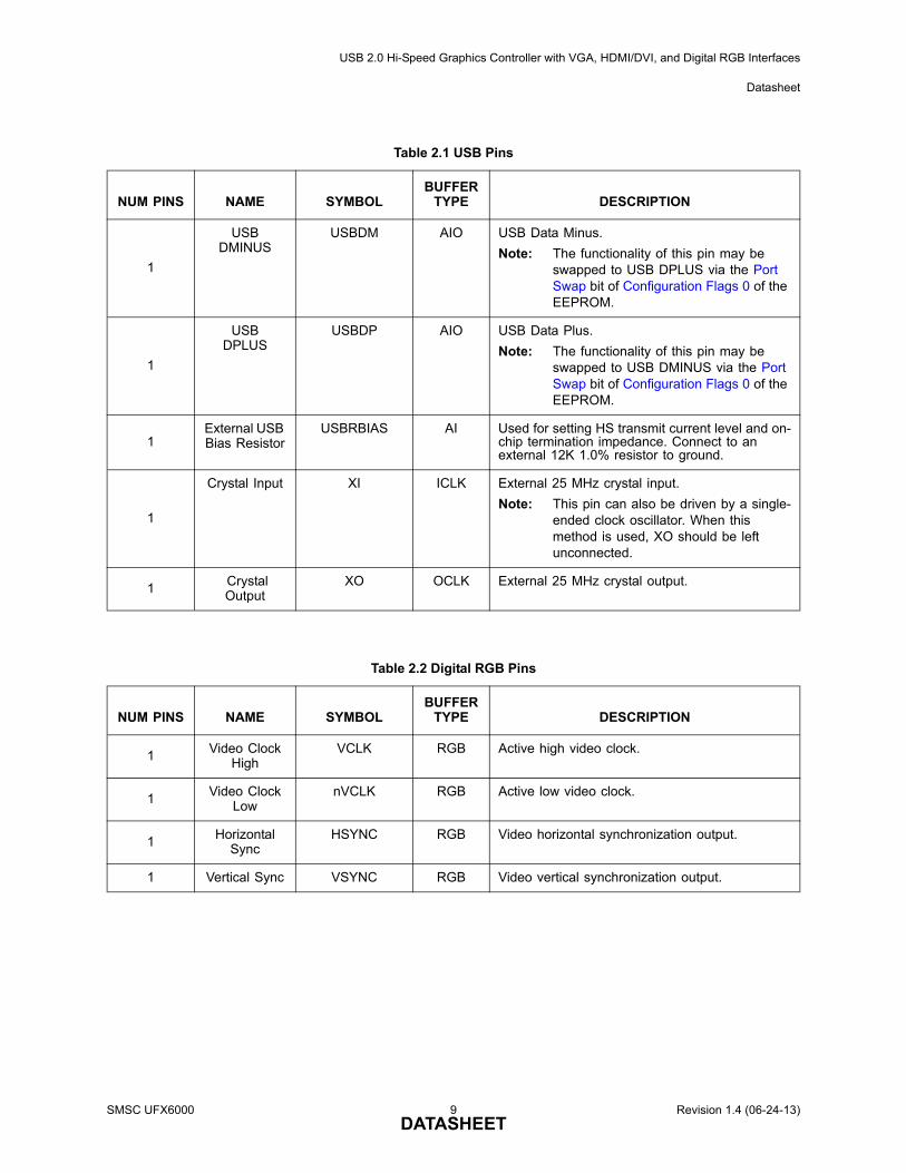
Table 2.1 USB Pins
NUM PINS NAME SYMBOLBUFFER
TYPE DESCRIPTION
1
USB DMINUS
USBDM AIO USB Data Minus.
Note: The functionality of this pin may be swapped to USB DPLUS via the Port Swap bit of Configuration Flags 0 of the EEPROM.
1
USBDPLUS
USBDP AIO USB Data Plus.
Note: The functionality of this pin may be swapped to USB DMINUS via the Port Swap bit of Configuration Flags 0 of the EEPROM.
1External USB Bias Resistor
USBRBIAS AI Used for setting HS transmit current level and on-chip termination impedance. Connect to an external 12K 1.0% resistor to ground.
1
Crystal Input XI ICLK External 25 MHz crystal input.
Note: This pin can also be driven by a single-ended clock oscillator. When this method is used, XO should be left unconnected.
1 Crystal Output
XO OCLK External 25 MHz crystal output.
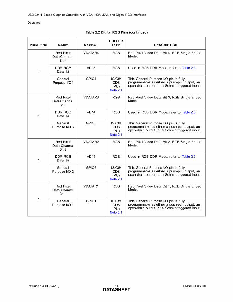
Table 2.2 Digital RGB Pins
NUM PINS NAME SYMBOLBUFFER
TYPE DESCRIPTION
1 Video Clock High
VCLK RGB Active high video clock.
1Video Clock
LownVCLK RGB Active low video clock.
1 Horizontal Sync
HSYNC RGB Video horizontal synchronization output.
1 Vertical Sync VSYNC RGB Video vertical synchronization output.
SMSC UFX6000 9 Revision 1.4 (06-24-13)DATASHEET
USB 2.0 Hi-Speed Graphics Controller with VGA, HDMI/DVI, and Digital RGB Interfaces
Datasheet
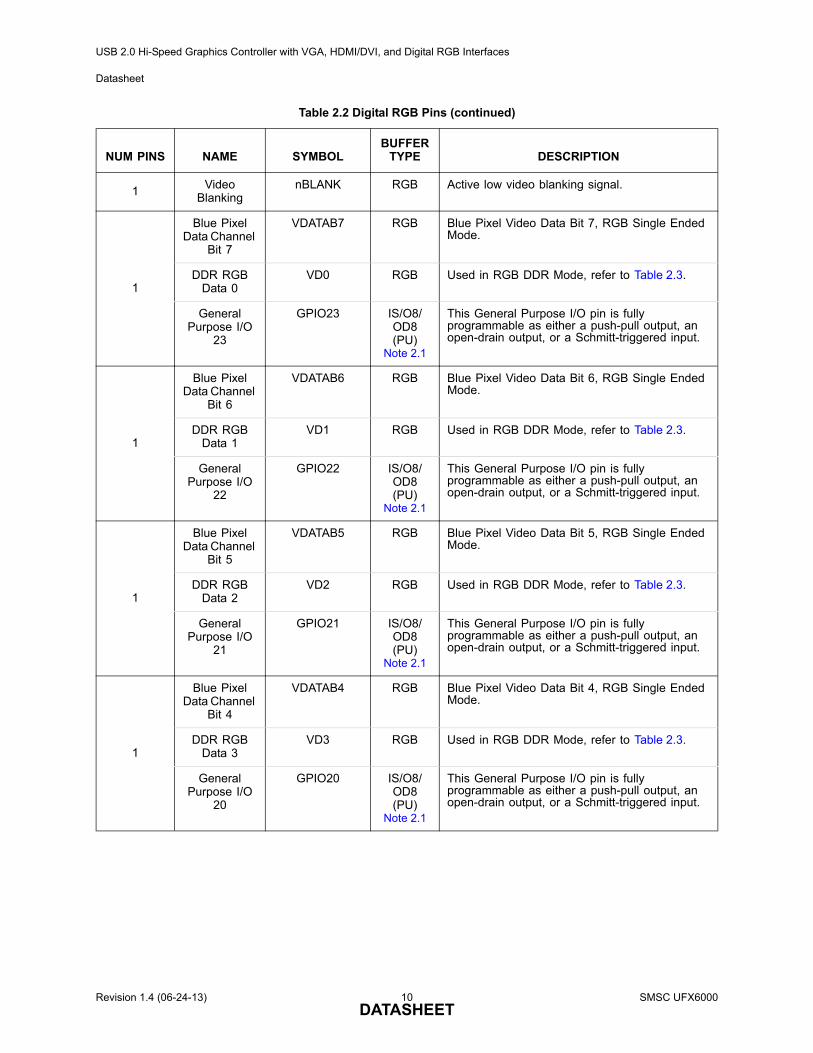
1Video
BlankingnBLANK RGB Active low video blanking signal.
1
Blue Pixel Data Channel
Bit 7
VDATAB7 RGB Blue Pixel Video Data Bit 7, RGB Single Ended Mode.
DDR RGB Data 0
VD0 RGB Used in RGB DDR Mode, refer to Table 2.3.
General Purpose I/O
23
GPIO23 IS/O8/OD8(PU)
Note 2.1
This General Purpose I/O pin is fully programmable as either a push-pull output, an open-drain output, or a Schmitt-triggered input.
1
Blue Pixel Data Channel
Bit 6
VDATAB6 RGB Blue Pixel Video Data Bit 6, RGB Single Ended Mode.
DDR RGB Data 1
VD1 RGB Used in RGB DDR Mode, refer to Table 2.3.
General Purpose I/O
22
GPIO22 IS/O8/OD8(PU)
Note 2.1
This General Purpose I/O pin is fully programmable as either a push-pull output, anopen-drain output, or a Schmitt-triggered input.
1
Blue Pixel Data Channel
Bit 5
VDATAB5 RGB Blue Pixel Video Data Bit 5, RGB Single Ended Mode.
DDR RGB Data 2
VD2 RGB Used in RGB DDR Mode, refer to Table 2.3.
General Purpose I/O
21
GPIO21 IS/O8/OD8(PU)
Note 2.1
This General Purpose I/O pin is fully programmable as either a push-pull output, an open-drain output, or a Schmitt-triggered input.
1
Blue Pixel Data Channel
Bit 4
VDATAB4 RGB Blue Pixel Video Data Bit 4, RGB Single Ended Mode.
DDR RGB Data 3
VD3 RGB Used in RGB DDR Mode, refer to Table 2.3.
General Purpose I/O
20
GPIO20 IS/O8/OD8(PU)
Note 2.1
This General Purpose I/O pin is fully programmable as either a push-pull output, an open-drain output, or a Schmitt-triggered input.
Table 2.2 Digital RGB Pins (continued)
NUM PINS NAME SYMBOLBUFFER
TYPE DESCRIPTION
Revision 1.4 (06-24-13) 10 SMSC UFX6000DATASHEET
USB 2.0 Hi-Speed Graphics Controller with VGA, HDMI/DVI, and Digital RGB Interfaces
Datasheet
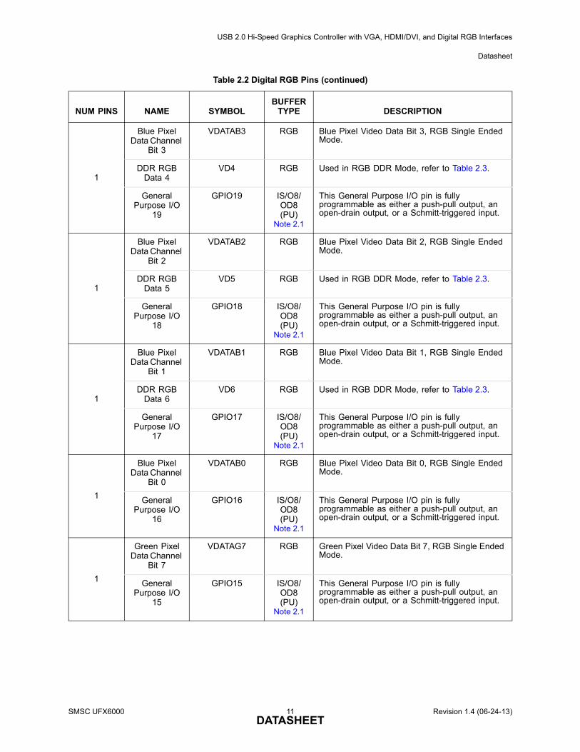
1
Blue Pixel Data Channel
Bit 3
VDATAB3 RGB Blue Pixel Video Data Bit 3, RGB Single Ended Mode.
DDR RGB Data 4
VD4 RGB Used in RGB DDR Mode, refer to Table 2.3.
General Purpose I/O
19
GPIO19 IS/O8/OD8(PU)
Note 2.1
This General Purpose I/O pin is fully programmable as either a push-pull output, an open-drain output, or a Schmitt-triggered input.
1
Blue Pixel Data Channel
Bit 2
VDATAB2 RGB Blue Pixel Video Data Bit 2, RGB Single Ended Mode.
DDR RGB Data 5
VD5 RGB Used in RGB DDR Mode, refer to Table 2.3.
General Purpose I/O
18
GPIO18 IS/O8/OD8(PU)
Note 2.1
This General Purpose I/O pin is fully programmable as either a push-pull output, an open-drain output, or a Schmitt-triggered input.
1
Blue Pixel Data Channel
Bit 1
VDATAB1 RGB Blue Pixel Video Data Bit 1, RGB Single Ended Mode.
DDR RGB Data 6
VD6 RGB Used in RGB DDR Mode, refer to Table 2.3.
General Purpose I/O
17
GPIO17 IS/O8/OD8(PU)
Note 2.1
This General Purpose I/O pin is fully programmable as either a push-pull output, an open-drain output, or a Schmitt-triggered input.
1
Blue Pixel Data Channel
Bit 0
VDATAB0 RGB Blue Pixel Video Data Bit 0, RGB Single Ended Mode.
General Purpose I/O
16
GPIO16 IS/O8/OD8(PU)
Note 2.1
This General Purpose I/O pin is fully programmable as either a push-pull output, an open-drain output, or a Schmitt-triggered input.
1
Green Pixel Data Channel
Bit 7
VDATAG7 RGB Green Pixel Video Data Bit 7, RGB Single Ended Mode.
General Purpose I/O
15
GPIO15 IS/O8/OD8(PU)
Note 2.1
This General Purpose I/O pin is fully programmable as either a push-pull output, an open-drain output, or a Schmitt-triggered input.
Table 2.2 Digital RGB Pins (continued)
NUM PINS NAME SYMBOLBUFFER
TYPE DESCRIPTION
SMSC UFX6000 11 Revision 1.4 (06-24-13)DATASHEET
USB 2.0 Hi-Speed Graphics Controller with VGA, HDMI/DVI, and Digital RGB Interfaces
Datasheet
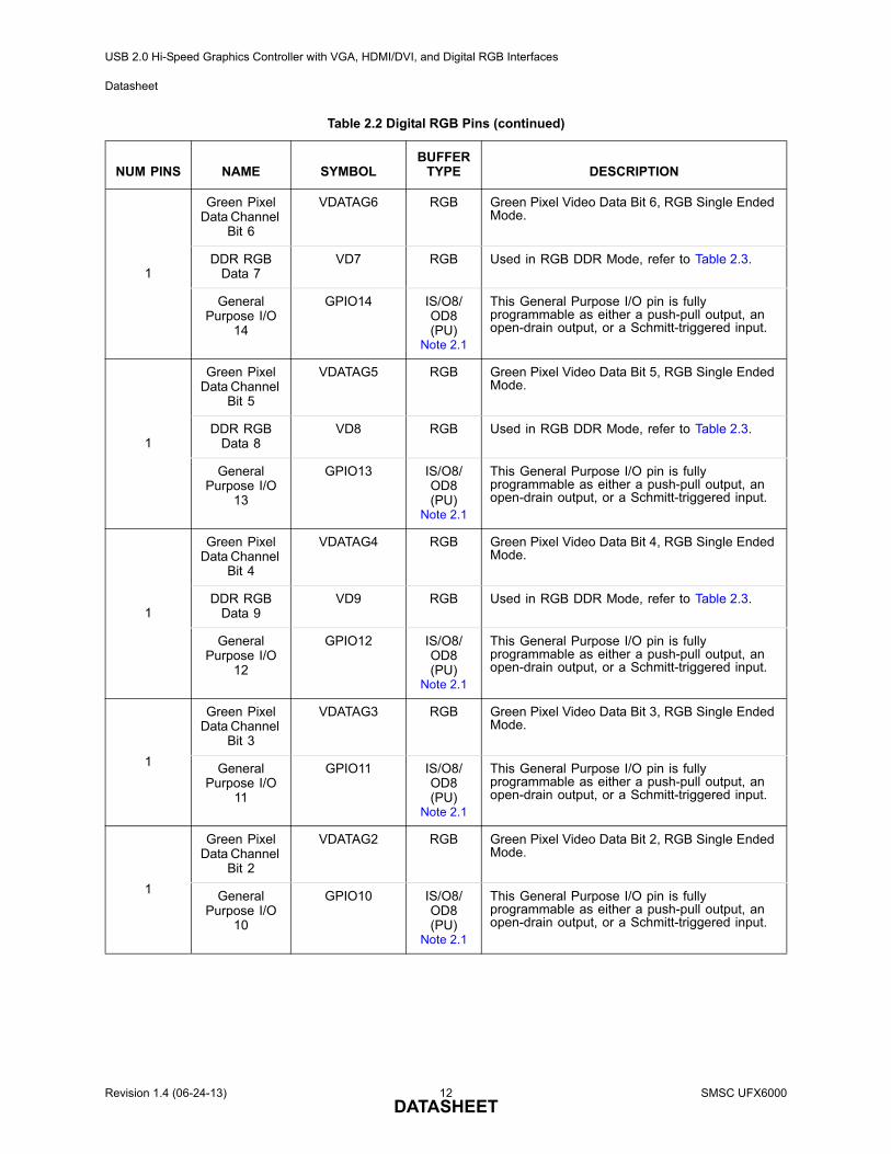
1
Green Pixel Data Channel
Bit 6
VDATAG6 RGB Green Pixel Video Data Bit 6, RGB Single Ended Mode.
DDR RGB Data 7
VD7 RGB Used in RGB DDR Mode, refer to Table 2.3.
General Purpose I/O
14
GPIO14 IS/O8/OD8(PU)
Note 2.1
This General Purpose I/O pin is fully programmable as either a push-pull output, an open-drain output, or a Schmitt-triggered input.
1
Green Pixel Data Channel
Bit 5
VDATAG5 RGB Green Pixel Video Data Bit 5, RGB Single Ended Mode.
DDR RGB Data 8
VD8 RGB Used in RGB DDR Mode, refer to Table 2.3.
General Purpose I/O
13
GPIO13 IS/O8/OD8(PU)
Note 2.1
This General Purpose I/O pin is fully programmable as either a push-pull output, an open-drain output, or a Schmitt-triggered input.
1
Green Pixel Data Channel
Bit 4
VDATAG4 RGB Green Pixel Video Data Bit 4, RGB Single Ended Mode.
DDR RGB Data 9
VD9 RGB Used in RGB DDR Mode, refer to Table 2.3.
General Purpose I/O
12
GPIO12 IS/O8/OD8(PU)
Note 2.1
This General Purpose I/O pin is fully programmable as either a push-pull output, an open-drain output, or a Schmitt-triggered input.
1
Green Pixel Data Channel
Bit 3
VDATAG3 RGB Green Pixel Video Data Bit 3, RGB Single Ended Mode.
General Purpose I/O
11
GPIO11 IS/O8/OD8(PU)
Note 2.1
This General Purpose I/O pin is fully programmable as either a push-pull output, an open-drain output, or a Schmitt-triggered input.
1
Green Pixel Data Channel
Bit 2
VDATAG2 RGB Green Pixel Video Data Bit 2, RGB Single Ended Mode.
General Purpose I/O
10
GPIO10 IS/O8/OD8(PU)
Note 2.1
This General Purpose I/O pin is fully programmable as either a push-pull output, an open-drain output, or a Schmitt-triggered input.
Table 2.2 Digital RGB Pins (continued)
NUM PINS NAME SYMBOLBUFFER
TYPE DESCRIPTION
Revision 1.4 (06-24-13) 12 SMSC UFX6000DATASHEET

USB 2.0 Hi-Speed Graphics Controller with VGA, HDMI/DVI, and Digital RGB Interfaces
Datasheet
1
Green Pixel Data Channel
Bit 1
VDATAG1 RGB Green Pixel Video Data Bit 1, RGB Single Ended Mode.
DDR RGB Data 10
VD10 RGB Used in RGB DDR Mode, refer to Table 2.3.
General Purpose I/O 9
GPIO9 IS/O8/OD8(PU)
Note 2.1
This General Purpose I/O pin is fully programmable as either a push-pull output, an open-drain output, or a Schmitt-triggered input.
1
Green Pixel Data Channel
Bit 0
VDATAG0 RGB Green Pixel Video Data Bit 0, RGB Single Ended Mode.
DDR RGB Data 11
VD11 RGB Used in RGB DDR Mode, refer to Table 2.3.
General Purpose I/O 8
GPIO8 IS/O8/OD8(PU)
Note 2.1
This General Purpose I/O pin is fully programmable as either a push-pull output, an open-drain output, or a Schmitt-triggered input.
1
Red Pixel Data Channel
Bit 7
VDATAR7 RGB Red Pixel Video Data Bit 7, RGB Single Ended Mode.
DDR RGB Data 12
VD12 RGB Used in RGB DDR Mode, refer to Table 2.3.
General Purpose I/O 7
GPIO7 IS/O8/OD8(PU)
Note 2.1
This General Purpose I/O pin is fully programmable as either a push-pull output, an open-drain output, or a Schmitt-triggered input.
1
Red Pixel Data Channel
Bit 6
VDATAR6 RGB Red Pixel Video Data Bit 6, RGB Single Ended Mode.
General Purpose I/O 6
GPIO6 IS/O8/OD8(PU)
Note 2.1
This General Purpose I/O pin is fully programmable as either a push-pull output, an open-drain output, or a Schmitt-triggered input.
1
Red Pixel Data Channel
Bit 5
VDATAR5 RGB Red Pixel Video Data Bit 5, RGB Single Ended Mode.
General Purpose I/O 5
GPIO5 IS/O8/OD8(PU)
Note 2.1
This General Purpose I/O pin is fully programmable as either a push-pull output, an open-drain output, or a Schmitt-triggered input.
Table 2.2 Digital RGB Pins (continued)
NUM PINS NAME SYMBOLBUFFER
TYPE DESCRIPTION
SMSC UFX6000 13 Revision 1.4 (06-24-13)DATASHEET
USB 2.0 Hi-Speed Graphics Controller with VGA, HDMI/DVI, and Digital RGB Interfaces
Datasheet
1
Red Pixel Data Channel
Bit 4
VDATAR4 RGB Red Pixel Video Data Bit 4, RGB Single Ended Mode.
DDR RGB Data 13
VD13 RGB Used in RGB DDR Mode, refer to Table 2.3.
General Purpose I/O4
GPIO4 IS/O8/OD8(PU)
Note 2.1
This General Purpose I/O pin is fully programmable as either a push-pull output, an open-drain output, or a Schmitt-triggered input.
1
Red Pixel Data Channel
Bit 3
VDATAR3 RGB Red Pixel Video Data Bit 3, RGB Single Ended Mode.
DDR RGB Data 14
VD14 RGB Used in RGB DDR Mode, refer to Table 2.3.
General Purpose I/O 3
GPIO3 IS/O8/OD8(PU)
Note 2.1
This General Purpose I/O pin is fully programmable as either a push-pull output, an open-drain output, or a Schmitt-triggered input.
1
Red Pixel Data Channel
Bit 2
VDATAR2 RGB Red Pixel Video Data Bit 2, RGB Single Ended Mode.
DDR RGB Data 15
VD15 RGB Used in RGB DDR Mode, refer to Table 2.3.
General Purpose I/O 2
GPIO2 IS/O8/OD8(PU)
Note 2.1
This General Purpose I/O pin is fully programmable as either a push-pull output, an open-drain output, or a Schmitt-triggered input.
1
Red Pixel Data Channel
Bit 1
VDATAR1 RGB Red Pixel Video Data Bit 1, RGB Single Ended Mode.
General Purpose I/O 1
GPIO1 IS/O8/OD8(PU)
Note 2.1
This General Purpose I/O pin is fully programmable as either a push-pull output, an open-drain output, or a Schmitt-triggered input.
Table 2.2 Digital RGB Pins (continued)
NUM PINS NAME SYMBOLBUFFER
TYPE DESCRIPTION
Revision 1.4 (06-24-13) 14 SMSC UFX6000DATASHEET
USB 2.0 Hi-Speed Graphics Controller with VGA, HDMI/DVI, and Digital RGB Interfaces
Datasheet
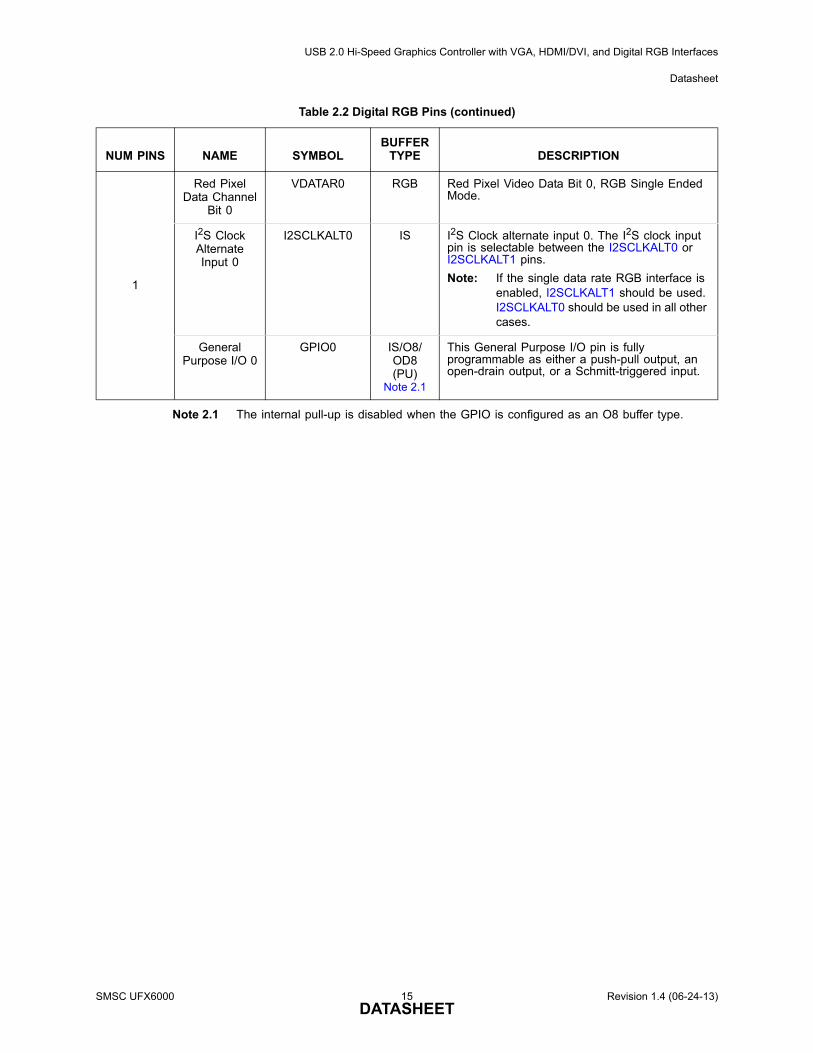
Note 2.1 The internal pull-up is disabled when the GPIO is configured as an O8 buffer type.
1
Red Pixel Data Channel
Bit 0
VDATAR0 RGB Red Pixel Video Data Bit 0, RGB Single Ended Mode.
I2S Clock Alternate Input 0
I2SCLKALT0 IS I2S Clock alternate input 0. The I2S clock input pin is selectable between the I2SCLKALT0 or I2SCLKALT1 pins.
Note: If the single data rate RGB interface is enabled, I2SCLKALT1 should be used. I2SCLKALT0 should be used in all other cases.
General Purpose I/O 0
GPIO0 IS/O8/OD8(PU)
Note 2.1
This General Purpose I/O pin is fully programmable as either a push-pull output, an open-drain output, or a Schmitt-triggered input.
Table 2.2 Digital RGB Pins (continued)
NUM PINS NAME SYMBOLBUFFER
TYPE DESCRIPTION
SMSC UFX6000 15 Revision 1.4 (06-24-13)DATASHEET
USB 2.0 Hi-Speed Graphics Controller with VGA, HDMI/DVI, and Digital RGB Interfaces
Datasheet
.
Table 2.3 RGB / DDR Mode Mapping Table
SDR(24-BIT MODE) DDR NAME
DDR (12-BIT MODE) DDR (15-BIT MODE)
VCLKRISING EDGE
VCLKFALLING EDGE
VCLKRISING EDGE
VCLKFALLING EDGE
VCLK
nVCLK
HSYNC
VSYNC
nBLANK
VDATAB7 VD0 - - BLUE0 GREEN5
VDATAB6 VD1 - - BLUE1 GREEN6
VDATAB5 VD2 BLUE0 GREEN4 BLUE2 GREEN7
VDATAB4 VD3 BLUE1 GREEN5 BLUE3 GREEN8
VDATAB3 VD4 BLUE2 GREEN6 BLUE4 GREEN9
VDATAB2 VD5 BLUE3 GREEN7 BLUE5 RED0
VDATAB1 VD6 BLUE4 RED0 BLUE6 RED1
VDATAB0 - - - - -
VDATAG7 - - - - -
VDATAG6 VD7 BLUE5 RED1 BLUE7 RED2
VDATAG5 VD8 BLUE6 RED2 BLUE8 RED3
VDATAG4 VD9 BLUE7 RED3 BLUE9 RED4
VDATAG3 - - - - -
VDATAG2 - - - - -
VDATAG1 VD10 - - GREEN0 RED5
VDATAG0 VD11 - - GREEN1 RED6
VDATAR7 VD12 GREEN0 RED4 GREEN2 RED7
VDATAR6 - - - - -
VDATAR5 - - - - -
VDATAR4 VD13 GREEN1 RED5 GREEN3 RED8
VDATAR3 VD14 GREEN2 RED6 GREEN4 RED9
VDATAR2 VD15 GREEN3 RED7 - -
VDATAR1 - - - - -
VDATAR0 - - - - -
Revision 1.4 (06-24-13) 16 SMSC UFX6000DATASHEET
USB 2.0 Hi-Speed Graphics Controller with VGA, HDMI/DVI, and Digital RGB Interfaces
Datasheet
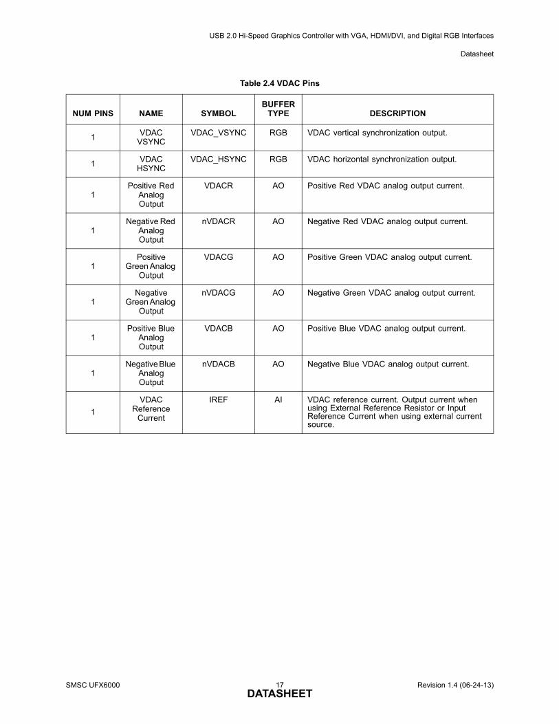
Table 2.4 VDAC Pins
NUM PINS NAME SYMBOLBUFFER
TYPE DESCRIPTION
1 VDAC VSYNC
VDAC_VSYNC RGB VDAC vertical synchronization output.
1 VDAC HSYNC
VDAC_HSYNC RGB VDAC horizontal synchronization output.
1Positive Red
Analog Output
VDACR AO Positive Red VDAC analog output current.
1Negative Red
Analog Output
nVDACR AO Negative Red VDAC analog output current.
1Positive
Green Analog Output
VDACG AO Positive Green VDAC analog output current.
1Negative
Green Analog Output
nVDACG AO Negative Green VDAC analog output current.
1Positive Blue
Analog Output
VDACB AO Positive Blue VDAC analog output current.
1Negative Blue
Analog Output
nVDACB AO Negative Blue VDAC analog output current.
1
VDAC Reference
Current
IREF AI VDAC reference current. Output current when using External Reference Resistor or Input Reference Current when using external current source.
SMSC UFX6000 17 Revision 1.4 (06-24-13)DATASHEET
USB 2.0 Hi-Speed Graphics Controller with VGA, HDMI/DVI, and Digital RGB Interfaces
Datasheet
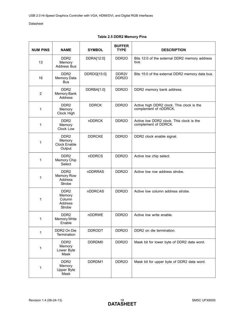
Table 2.5 DDR2 Memory Pins
NUM PINS NAME SYMBOLBUFFER
TYPE DESCRIPTION
13DDR2
Memory Address Bus
DDRA[12:0] DDR2O Bits 12:0 of the external DDR2 memory address bus.
16DDR2
Memory Data Bus
DDRDQ[15:0] DDR2I/ DDR2O
Bits 15:0 of the external DDR2 memory data bus.
2DDR2
Memory Bank Address
DDRBA[1:0] DDR2O DDR2 memory bank address.
1DDR2
Memory Clock High
DDRCK DDR2O Active high DDR2 clock. This clock is the complement of nDDRCK.
1DDR2
Memory Clock Low
nDDRCK DDR2O Active low DDR2 clock. This clock is the complement of DDRCK.
1
DDR2 Memory
Clock Enable Output
DDRCKE DDR2O DDR2 clock enable signal.
1DDR2
Memory Chip Select
nDDRCS DDR2O Active low chip select.
1
DDR2 Memory Row
Address Strobe
nDDRRAS DDR2O Active low row address strobe.
1
DDR2 Memory Column Address Strobe
nDDRCAS DDR2O Active low column address strobe.
1DDR2
Memory Write Enable
nDDRWE DDR2O Active low write enable.
1 DDR2 On Die Termination
DDRODT DDR2O DDR2 on die termination.
1
DDR2 Memory
Lower Byte Mask
DDRDM0 DDR2O Mask bit for lower byte of DDR2 data word.
1
DDR2 Memory
Upper Byte Mask
DDRDM1 DDR2O Mask bit for upper byte of DDR2 data word.
Revision 1.4 (06-24-13) 18 SMSC UFX6000DATASHEET
USB 2.0 Hi-Speed Graphics Controller with VGA, HDMI/DVI, and Digital RGB Interfaces
Datasheet
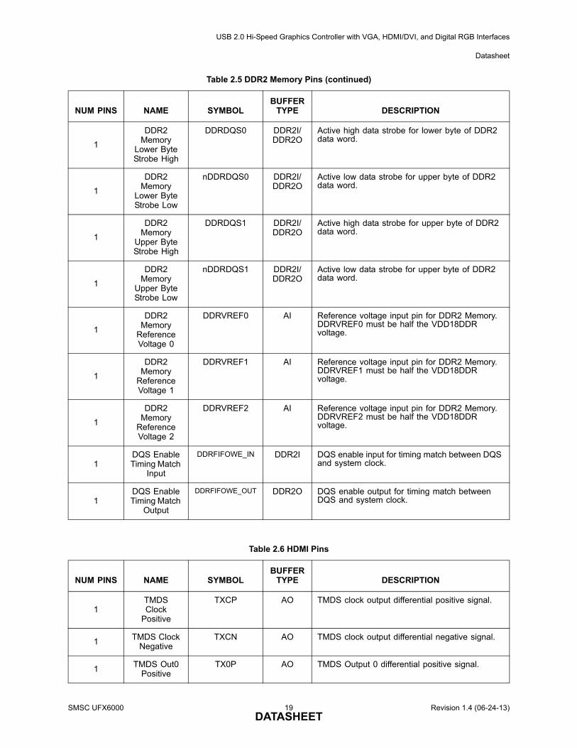
1
DDR2 Memory
Lower Byte Strobe High
DDRDQS0 DDR2I/ DDR2O
Active high data strobe for lower byte of DDR2 data word.
1
DDR2 Memory
Lower Byte Strobe Low
nDDRDQS0 DDR2I/ DDR2O
Active low data strobe for upper byte of DDR2 data word.
1
DDR2 Memory
Upper Byte Strobe High
DDRDQS1 DDR2I/ DDR2O
Active high data strobe for upper byte of DDR2 data word.
1
DDR2 Memory
Upper Byte Strobe Low
nDDRDQS1 DDR2I/ DDR2O
Active low data strobe for upper byte of DDR2 data word.
1
DDR2 Memory
Reference Voltage 0
DDRVREF0 AI Reference voltage input pin for DDR2 Memory. DDRVREF0 must be half the VDD18DDR voltage.
1
DDR2 Memory
Reference Voltage 1
DDRVREF1 AI Reference voltage input pin for DDR2 Memory. DDRVREF1 must be half the VDD18DDR voltage.
1
DDR2 Memory
Reference Voltage 2
DDRVREF2 AI Reference voltage input pin for DDR2 Memory. DDRVREF2 must be half the VDD18DDR voltage.
1DQS Enable Timing Match
Input
DDRFIFOWE_IN DDR2I DQS enable input for timing match between DQS and system clock.
1DQS Enable Timing Match
Output
DDRFIFOWE_OUT DDR2O DQS enable output for timing match between DQS and system clock.
Table 2.6 HDMI Pins
NUM PINS NAME SYMBOLBUFFER
TYPE DESCRIPTION
1TMDSClock
Positive
TXCP AO TMDS clock output differential positive signal.
1 TMDS Clock Negative
TXCN AO TMDS clock output differential negative signal.
1 TMDS Out0 Positive
TX0P AO TMDS Output 0 differential positive signal.
Table 2.5 DDR2 Memory Pins (continued)
NUM PINS NAME SYMBOLBUFFER
TYPE DESCRIPTION
SMSC UFX6000 19 Revision 1.4 (06-24-13)DATASHEET
USB 2.0 Hi-Speed Graphics Controller with VGA, HDMI/DVI, and Digital RGB Interfaces
Datasheet
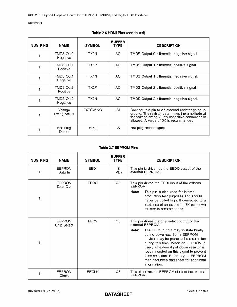
1TMDS Out0
NegativeTX0N AO TMDS Output 0 differential negative signal.
1 TMDS Out1 Positive
TX1P AO TMDS Output 1 differential positive signal.
1TMDS Out1
NegativeTX1N AO TMDS Output 1 differential negative signal.
1 TMDS Out2 Positive
TX2P AO TMDS Output 2 differential positive signal.
1 TMDS Out2 Negative
TX2N AO TMDS Output 2 differential negative signal.
1
Voltage Swing Adjust
EXTSWING AI Connect this pin to an external resistor going to ground. The resistor determines the amplitude of the voltage swing. A low capacitive connection is allowed. A value of 5K is recommended.
1 Hot Plug Detect
HPD IS Hot plug detect signal.
Table 2.7 EEPROM Pins
NUM PINS NAME SYMBOLBUFFER
TYPE DESCRIPTION
1EEPROM Data In
EEDI IS(PD)
This pin is driven by the EEDO output of the external EEPROM.
1
EEPROM Data Out
EEDO O8 This pin drives the EEDI input of the external EEPROM.
Note: This pin is also used for internal production test purposes and should never be pulled high. If connected to a load, use of an external 4.7K pull-down resistor is recommended.
1
EEPROM Chip Select
EECS O8 This pin drives the chip select output of the external EEPROM.
Note: The EECS output may tri-state briefly during power-up. Some EEPROM devices may be prone to false selection during this time. When an EEPROM is used, an external pull-down resistor is recommended on this signal to prevent false selection. Refer to your EEPROM manufacturer’s datasheet for additional information.
1 EEPROM Clock
EECLK O8 This pin drives the EEPROM clock of the external EEPROM.
Table 2.6 HDMI Pins (continued)
NUM PINS NAME SYMBOLBUFFER
TYPE DESCRIPTION
Revision 1.4 (06-24-13) 20 SMSC UFX6000DATASHEET
USB 2.0 Hi-Speed Graphics Controller with VGA, HDMI/DVI, and Digital RGB Interfaces
Datasheet
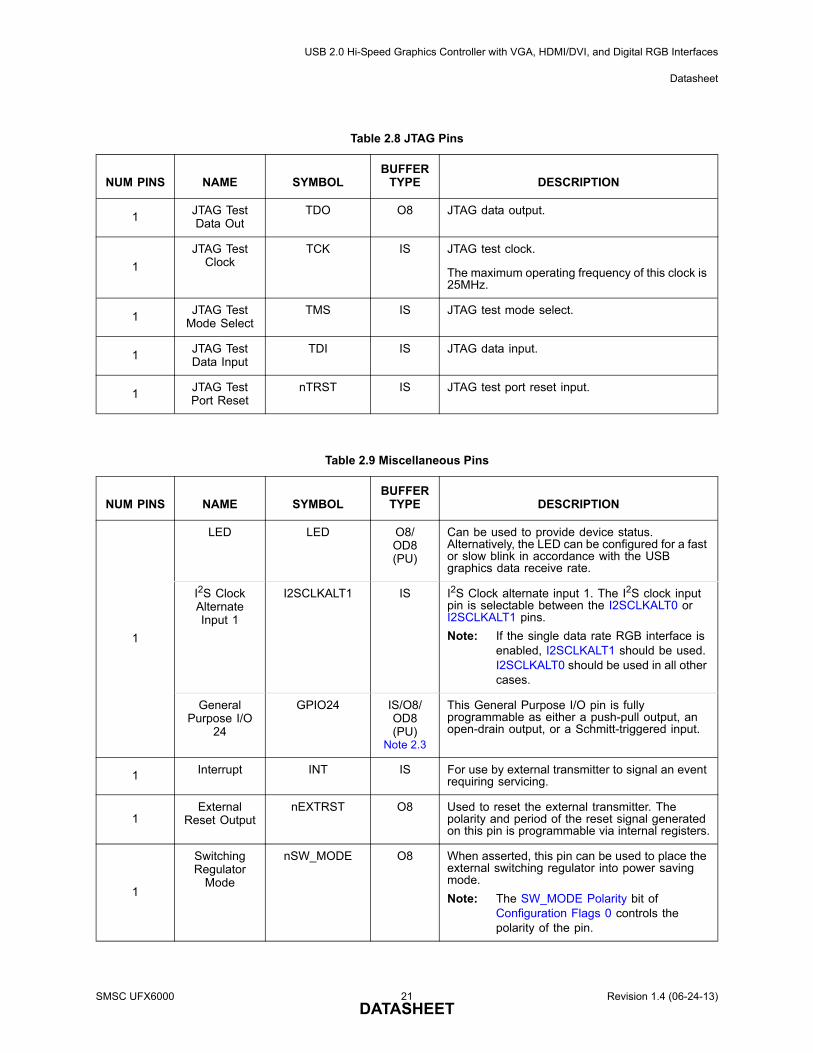
Table 2.8 JTAG Pins
NUM PINS NAME SYMBOLBUFFER
TYPE DESCRIPTION
1JTAG Test Data Out
TDO O8 JTAG data output.
1
JTAG Test Clock
TCK IS JTAG test clock.
The maximum operating frequency of this clock is 25MHz.
1JTAG Test
Mode SelectTMS IS JTAG test mode select.
1 JTAG Test Data Input
TDI IS JTAG data input.
1JTAG Test Port Reset
nTRST IS JTAG test port reset input.
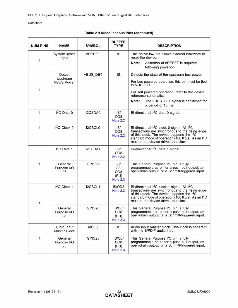
Table 2.9 Miscellaneous Pins
NUM PINS NAME SYMBOLBUFFER
TYPE DESCRIPTION
1
LED LED O8/OD8(PU)
Can be used to provide device status. Alternatively, the LED can be configured for a fast or slow blink in accordance with the USB graphics data receive rate.
I2S Clock Alternate Input 1
I2SCLKALT1 IS I2S Clock alternate input 1. The I2S clock input pin is selectable between the I2SCLKALT0 or I2SCLKALT1 pins.
Note: If the single data rate RGB interface is enabled, I2SCLKALT1 should be used. I2SCLKALT0 should be used in all other cases.
General Purpose I/O
24
GPIO24 IS/O8/OD8(PU)
Note 2.3
This General Purpose I/O pin is fully programmable as either a push-pull output, an open-drain output, or a Schmitt-triggered input.
1 Interrupt INT IS For use by external transmitter to signal an event requiring servicing.
1External
Reset OutputnEXTRST O8 Used to reset the external transmitter. The
polarity and period of the reset signal generated on this pin is programmable via internal registers.
1
Switching Regulator
Mode
nSW_MODE O8 When asserted, this pin can be used to place the external switching regulator into power saving mode.
Note: The SW_MODE Polarity bit of Configuration Flags 0 controls the polarity of the pin.
SMSC UFX6000 21 Revision 1.4 (06-24-13)DATASHEET
USB 2.0 Hi-Speed Graphics Controller with VGA, HDMI/DVI, and Digital RGB Interfaces
Datasheet
1
System Reset Input
nRESET IS This active-low pin allows external hardware to reset the device.
Note: Assertion of nRESET is required following power-on.
1
Detect Upstream
VBUS Power
VBUS_DET IS Detects the state of the upstream bus power.
For bus powered operation, this pin must be tied to VDD33IO.
For self powered operation, refer to the device reference schematics.
Note: The VBUS_DET signal is deglitched for a period of 10 ms.
1 I2C Data 0 I2CSDA0 IS/OD8
Note 2.2
Bi-directional I2C data 0 signal.
1 I2C Clock 0 I2CSCL0 IS/OD8
Note 2.2
Bi-directional I2C clock 0 signal. All I2C transactions are synchronous to the rising edge of this clock. The device supports the I2C standard mode of operation (100 Kb/s). As an I2C master, the device drives this clock.
1
I2C Data 1 I2CSDA1 IS/OD8
Note 2.2
Bi-directional I2C data 1 signal.
General Purpose I/O
27
GPIO27 IS/O8/OD8(PU)
Note 2.3
This General Purpose I/O pin is fully programmable as either a push-pull output, an open-drain output, or a Schmitt-triggered input.
1
I2C Clock 1 I2CSCL1 IS/OD8Note 2.2
Bi-directional I2C clock 1 signal. All I2C transactions are synchronous to the rising edge of this clock. The device supports the I2C standard mode of operation (100 Kb/s). As an I2C master, the device drives this clock.
General Purpose I/O
28
GPIO28 IS/O8/OD8(PU)
Note 2.3
This General Purpose I/O pin is fully programmable as either a push-pull output, an open-drain output, or a Schmitt-triggered input.
1
Audio Input Master Clock
MCLK IS Audio input master clock. This clock is coherent with the S/PDIF audio input.
General Purpose I/O
25
GPIO25 IS/O8/OD8(PU)
Note 2.3
This General Purpose I/O pin is fully programmable as either a push-pull output, an open-drain output, or a Schmitt-triggered input.
Table 2.9 Miscellaneous Pins (continued)
NUM PINS NAME SYMBOLBUFFER
TYPE DESCRIPTION
Revision 1.4 (06-24-13) 22 SMSC UFX6000DATASHEET
USB 2.0 Hi-Speed Graphics Controller with VGA, HDMI/DVI, and Digital RGB Interfaces
Datasheet
Note 2.2 If unused, this signal must be pulled to a valid state.
Note 2.3 The internal pull-up is disabled when the GPIO is configured as an O8 buffer type.
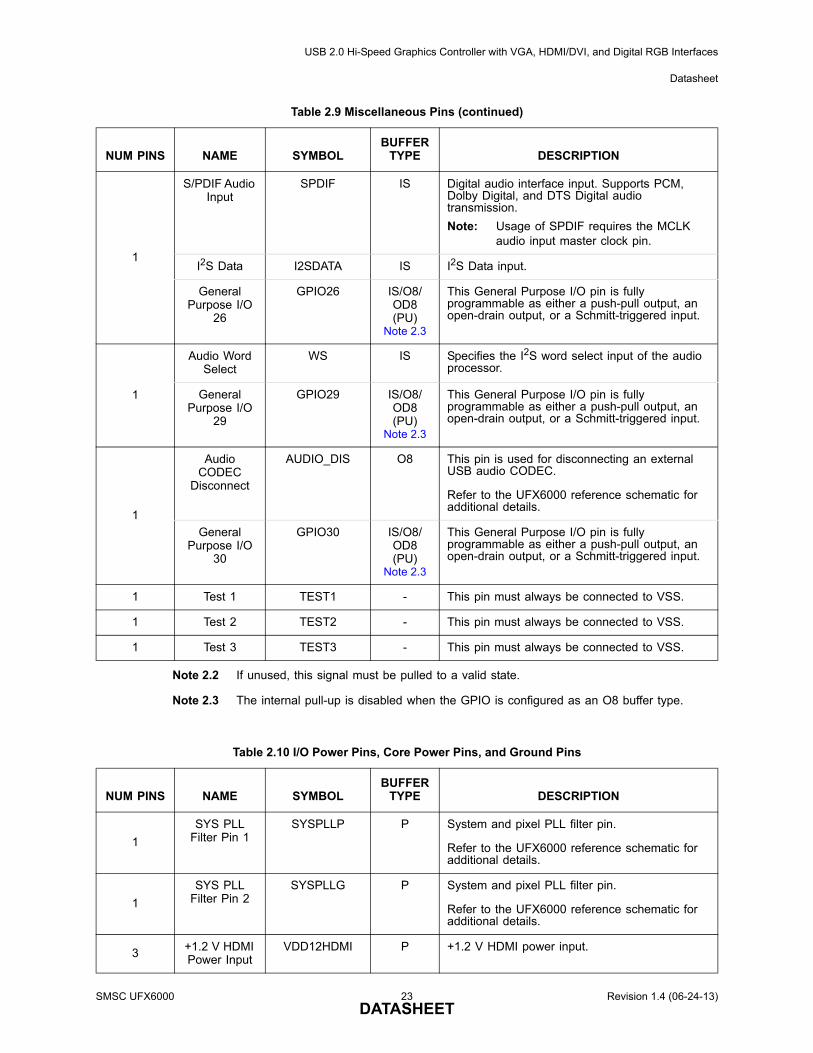
1
S/PDIF Audio Input
SPDIF IS Digital audio interface input. Supports PCM, Dolby Digital, and DTS Digital audio transmission.
Note: Usage of SPDIF requires the MCLK audio input master clock pin.
I2S Data I2SDATA IS I2S Data input.
General Purpose I/O
26
GPIO26 IS/O8/OD8(PU)
Note 2.3
This General Purpose I/O pin is fully programmable as either a push-pull output, an open-drain output, or a Schmitt-triggered input.
1
Audio Word Select
WS IS Specifies the I2S word select input of the audio processor.
General Purpose I/O
29
GPIO29 IS/O8/OD8(PU)
Note 2.3
This General Purpose I/O pin is fully programmable as either a push-pull output, an open-drain output, or a Schmitt-triggered input.
1
Audio CODEC
Disconnect
AUDIO_DIS O8 This pin is used for disconnecting an external USB audio CODEC.
Refer to the UFX6000 reference schematic for additional details.
GeneralPurpose I/O
30
GPIO30 IS/O8/OD8(PU)
Note 2.3
This General Purpose I/O pin is fully programmable as either a push-pull output, an open-drain output, or a Schmitt-triggered input.
1 Test 1 TEST1 - This pin must always be connected to VSS.
1 Test 2 TEST2 - This pin must always be connected to VSS.
1 Test 3 TEST3 - This pin must always be connected to VSS.
Table 2.10 I/O Power Pins, Core Power Pins, and Ground Pins
NUM PINS NAME SYMBOLBUFFER
TYPE DESCRIPTION
1
SYS PLL Filter Pin 1
SYSPLLP P System and pixel PLL filter pin.
Refer to the UFX6000 reference schematic for additional details.
1
SYS PLL Filter Pin 2
SYSPLLG P System and pixel PLL filter pin.
Refer to the UFX6000 reference schematic for additional details.
3 +1.2 V HDMI Power Input
VDD12HDMI P +1.2 V HDMI power input.
Table 2.9 Miscellaneous Pins (continued)
NUM PINS NAME SYMBOLBUFFER
TYPE DESCRIPTION
SMSC UFX6000 23 Revision 1.4 (06-24-13)DATASHEET
USB 2.0 Hi-Speed Graphics Controller with VGA, HDMI/DVI, and Digital RGB Interfaces
Datasheet
Note 2.4 Refer to Chapter 3, "Power Connections," on page 29 and the device reference schematicsfor additional power connection information.
3 HDMI Ground VSSHDMI P HDMI ground.
3+3.3 V VDAC Power Input
VDD33VDAC P +3.3 V Video DAC power input. (Note 2.4)
1+3.3 V VDAC
Reference Input
VDACREF P +3.3 V Video DAC reference voltage input. (Note 2.4)
2 VDAC Ground
VSSVDAC P Video DAC ground.
1 +3.3 V USB Power Input
VDD33USB P +3.3 V USB power input. (Note 2.4)
1+1.2 V USB PLL Supply
Input
VDD12USBPLL P +1.2 V USB PLL supply input. (Note 2.4)
15+1.8 V DDR2 Power Input
VDD18DDR P +1.8 V DDR2 power input. (Note 2.4)
8+3.3 V I/O
Power InputVDD33IO P +3.3 V I/O power input. (Note 2.4)
11+1.2 V Digital Core Power
Input
VDD12CORE P +1.2 V digital core power input. (Note 2.4)
37 Ground VSS P Common Ground.
Table 2.11 No-Connect Pins
NUM PINS NAME SYMBOLBUFFER
TYPE DESCRIPTION
9 No Connect NC - These pins must be left floating for normal device operation.
Table 2.10 I/O Power Pins, Core Power Pins, and Ground Pins (continued)
NUM PINS NAME SYMBOLBUFFER
TYPE DESCRIPTION
Revision 1.4 (06-24-13) 24 SMSC UFX6000DATASHEET
USB 2.0 Hi-Speed Graphics Controller with VGA, HDMI/DVI, and Digital RGB Interfaces
Datasheet
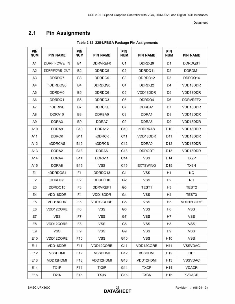
2.1 Pin Assignments
Table 2.12 225-LFBGA Package Pin Assignments
PINNUM PIN NAME
PINNUM PIN NAME
PINNUM PIN NAME
PINNUM PIN NAME
A1 DDRFIFOWE_IN B1 DDRVREF0 C1 DDRDQ9 D1 DDRDQS1
A2 DDRFIFOWE_OUT B2 DDRDQ5 C2 DDRDQ11 D2 DDRDM1
A3 DDRDQ7 B3 DDRDQ0 C3 DDRDQ12 D3 DDRDQ14
A4 nDDRDQS0 B4 DDRDQS0 C4 DDRDQ2 D4 VDD18DDR
A5 DDRDM0 B5 DDRDQ6 C5 VDD18DDR D5 VDD18DDR
A6 DDRDQ1 B6 DDRDQ3 C6 DDRDQ4 D6 DDRVREF2
A7 nDDRWE B7 DDRCKE C7 DDRBA1 D7 VDD18DDR
A8 DDRA10 B8 DDRBA0 C8 DDRA1 D8 VDD18DDR
A9 DDRA3 B9 DDRA7 C9 DDRA5 D9 VDD18DDR
A10 DDRA9 B10 DDRA12 C10 nDDRRAS D10 VDD18DDR
A11 DDRCK B11 nDDRCK C11 VDD18DDR D11 VDD18DDR
A12 nDDRCAS B12 nDDRCS C12 DDRA0 D12 VDD18DDR
A13 DDRA2 B13 DDRA6 C13 DDRODT D13 VDD18DDR
A14 DDRA4 B14 DDRA11 C14 VSS D14 TX2P
A15 DDRA8 B15 VSS C15 EXTSWING D15 TX2N
E1 nDDRDQS1 F1 DDRDQ13 G1 VSS H1 NC
E2 DDRDQ8 F2 DDRDQ10 G2 VSS H2 NC
E3 DDRDQ15 F3 DDRVREF1 G3 TEST1 H3 TEST2
E4 VDD18DDR F4 VDD18DDR G4 VSS H4 TEST3
E5 VDD18DDR F5 VDD12CORE G5 VSS H5 VDD12CORE
E6 VDD12CORE F6 VSS G6 VSS H6 VSS
E7 VSS F7 VSS G7 VSS H7 VSS
E8 VDD12CORE F8 VSS G8 VSS H8 VSS
E9 VSS F9 VSS G9 VSS H9 VSS
E10 VDD12CORE F10 VSS G10 VSS H10 VSS
E11 VDD18DDR F11 VDD12CORE G11 VDD12CORE H11 VSSVDAC
E12 VSSHDMI F12 VSSHDMI G12 VSSHDMI H12 IREF
E13 VDD12HDMI F13 VDD12HDMI G13 VDD12HDMI H13 VSSVDAC
E14 TX1P F14 TX0P G14 TXCP H14 VDACR
E15 TX1N F15 TX0N G15 TXCN H15 nVDACR
SMSC UFX6000 25 Revision 1.4 (06-24-13)DATASHEET
USB 2.0 Hi-Speed Graphics Controller with VGA, HDMI/DVI, and Digital RGB Interfaces
Datasheet
J1 NC K1 I2CSDA1/GPIO27
L1 USBDP M1 VDD33USB
J2 NC K2 I2CSDA0 L2 USBDM M2 NC
J3 VSS K3 I2CSCL1/GPIO28
L3 VBUS_DET M3 HPD
J4 NC K4 I2CSCL0 L4 AUDIO_DIS/GPIO30
M4 VDATAB4/VD3/GPIO20
J5 VSS K5 VDD12CORE L5 VDD33IO M5 VDD33IO
J6 VSS K6 VSS L6 VDD12CORE M6 VDD33IO
J7 VSS K7 VSS L7 VSS M7 VDD33IO
J8 VSS K8 VSS L8 VDD12CORE M8 VDATAG4/VD9/GPIO12
J9 VSS K9 VSS L9 VSS M9 VDD33IO
J10 VSS K10 VSS L10 VDD12CORE M10 VDATAR5/GPIO5
J11 VDD33VDAC K11 VDACREF L11 VDD33IO M11 VDD33IO
J12 VDD33VDAC K12 VDAC_HSYNC L12 VDD33IO M12 TDI
J13 VDD33VDAC K13 VDAC_VSYNC L13 WS/GPIO29 M13 INT
J14 VDACG K14 VDACB L14 MCLK/GPIO25 M14 EECS
J15 nVDACG K15 nVDACB L15 SPDIF/I2SDATA/GPIO26
M15 EECLK
Table 2.12 225-LFBGA Package Pin Assignments (continued)
PINNUM PIN NAME
PINNUM PIN NAME
PINNUM PIN NAME
PINNUM PIN NAME
Revision 1.4 (06-24-13) 26 SMSC UFX6000DATASHEET
USB 2.0 Hi-Speed Graphics Controller with VGA, HDMI/DVI, and Digital RGB Interfaces
Datasheet
N1 XI P1 XO R1 SYSPLLP
N2 VDD12USBPLL P2 SYSPLLG R2 VDATAB7/VD0/GPIO23
N3 USBRBIAS P3 VDATAB6/VD1/GPIO22
R3 VDATAB5/VD2/GPIO21
N4 VDATAB3/VD4/GPIO19
P4 VDATAB2/VD5/GPIO18
R4 VDATAB1/VD6/GPIO17
N5 VDATAB0/GPIO16
P5 HSYNC R5 VSYNC
N6 nBLANK P6 nVCLK R6 VCLK
N7 VDATAG7/GPIO15
P7 VDATAG6/VD7/GPIO14
R7 VDATAG5/VD8/GPIO13
N8 VDATAG3/GPIO11
P8 VDATAG2/GPIO10
R8 VDATAG1/VD10/GPIO9
N9 VDATAG0/VD11/GPIO8
P9 VDATAR7/VD12/GPIO7
R9 VDATAR6/GPIO6
N10 VDATAR4/VD13/GPIO4
P10 VDATAR3/VD14/GPIO3
R10 VDATAR2/VD15/GPIO2
N11 VDATAR1/GPIO1
P11 VDATAR0/I2SCLKALT0/
GPIO0
R11 nTRST
N12 TDO P12 TCK R12 TMS
N13 nEXTRST P13 nSW_MODE R13 NC
N14 NC P14 nRESET R14 LED/I2SCLKALT1/
GPIO24
N15 NC P15 EEDI R15 EEDO
Table 2.12 225-LFBGA Package Pin Assignments (continued)
PINNUM PIN NAME
PINNUM PIN NAME
PINNUM PIN NAME
PINNUM PIN NAME
SMSC UFX6000 27 Revision 1.4 (06-24-13)DATASHEET
USB 2.0 Hi-Speed Graphics Controller with VGA, HDMI/DVI, and Digital RGB Interfaces
Datasheet
2.2 Buffer Types
Table 2.13 Buffer Types
BUFFER TYPE DESCRIPTION
IS Schmitt-triggered Input
O8 Output with 8mA sink and 8mA source
OD8 Open-drain output with 8mA sink
O12 Output with 12mA sink and 12mA source
OD12 Open-drain output with 12mA sink
PU 50uA (typical) internal pull-up. Unless otherwise noted in the pin description, internal pull-ups are always enabled.
Note: Internal pull-up resistors prevent unconnected inputs from floating. Do not rely on internal resistors to drive signals external to the device. When connected to a load that must be pulled high, an external resistor must be added.
PD 50uA (typical) internal pull-down. Unless otherwise noted in the pin description, internal pull-downs are always enabled.
Note: Internal pull-down resistors prevent unconnected inputs from floating. Do not rely on internal resistors to drive signals external to the device. When connected to a load that must be pulled low, an external resistor must be added.
AI Analog input
AO Analog output
AIO Analog bi-directional
DDR2I DDR2 input
DDR2O DDR2 output
RGB RGB output
ICLK Crystal oscillator input pin
OCLK Crystal oscillator output pin
P Power pin
Revision 1.4 (06-24-13) 28 SMSC UFX6000DATASHEET
USB 2.0 Hi-Speed Graphics Controller with VGA, HDMI/DVI, and Digital RGB Interfaces
Datasheet
SMSC UFX6000 29 Revision 1.4 (06-24-13)DATASHEET
Chapter 3 Power Connections
Figure 3.1 illustrates the power connections for UFX6000.
Note: For additional power connection information, refer to the UFX6000 reference schematic.
Figure 3.1 Power Connections
VDD12USBPLL
UFX6000
VDD18DDR (x15)10uF
0.1uF(x5)
0.01uF(x7)
VDD12HDMI (x3)
VDD12CORE (x11)
+1.
8V C
onn
ectio
ns
10uF
0.1uF(x10)
+1.8V
+1.2V
TEST1
1.0uF
0.1uF(x2)
1.0uF
0.1uF
+1.
2V C
onn
ect
ions
10uF
0.1uF(x7)
+3.3V
1.0uF
0.1uF(x2)
1.0uF
0.1uF
+3.
3V C
onn
ectio
ns
VDD33USB
VDD33VDAC (x3)
VDD33IO (x8)
VDACAnalogGround
VSSVDAC (x2)
VSSHDMI (x3)
VSS (x37)
Gro
und
s
VDAC Analog Ground
SYSPLLP
SYSPLLG
0.1uF22uF
100Ohm
TEST2
TEST3
USB 2.0 Hi-Speed Graphics Controller with VGA, HDMI/DVI, and Digital RGB Interfaces
Datasheet
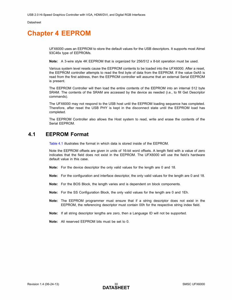
Chapter 4 EEPROM
UFX6000 uses an EEPROM to store the default values for the USB descriptors. It supports most Atmel93C46x type of EEPROMs.
Note: A 3-wire style 4K EEPROM that is organized for 256/512 x 8-bit operation must be used.
Various system level resets cause the EEPROM contents to be loaded into the UFX6000. After a reset,the EEPROM controller attempts to read the first byte of data from the EEPROM. If the value 0xA5 isread from the first address, then the EEPROM controller will assume that an external Serial EEPROMis present.
The EEPROM Controller will then load the entire contents of the EEPROM into an internal 512 byteSRAM. The contents of the SRAM are accessed by the device as needed (i.e., to fill Get Descriptorcommands).
The UFX6000 may not respond to the USB host until the EEPROM loading sequence has completed.Therefore, after reset the USB PHY is kept in the disconnect state until the EEPROM load hascompleted.
The EEPROM Controller also allows the Host system to read, write and erase the contents of theSerial EEPROM.
4.1 EEPROM Format
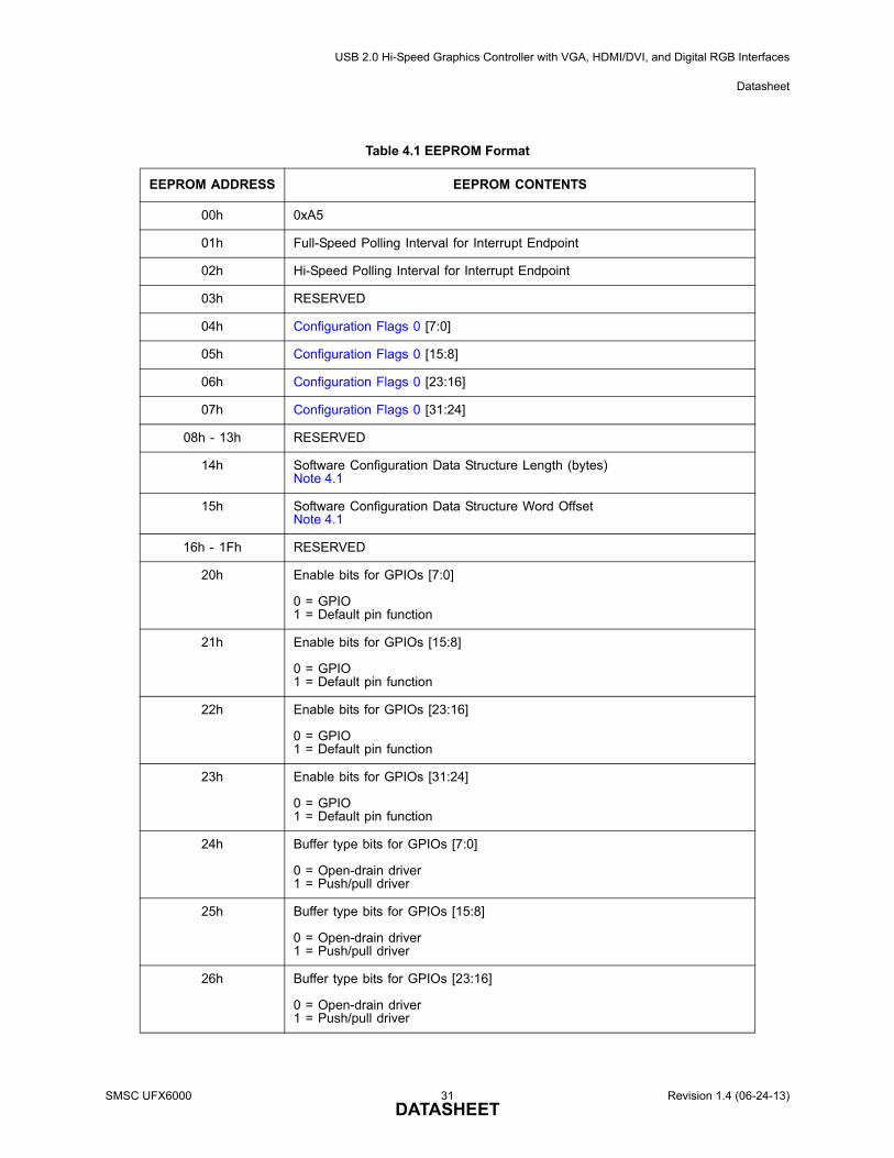
Table 4.1 illustrates the format in which data is stored inside of the EEPROM.
Note the EEPROM offsets are given in units of 16-bit word offsets. A length field with a value of zeroindicates that the field does not exist in the EEPROM. The UFX6000 will use the field’s hardwaredefault value in this case.
Note: For the device descriptor the only valid values for the length are 0 and 18.
Note: For the configuration and interface descriptor, the only valid values for the length are 0 and 18.
Note: For the BOS Block, the length varies and is dependent on block components.
Note: For the SS Configuration Block, the only valid values for the length are 0 and 1Eh.
Note: The EEPROM programmer must ensure that if a string descriptor does not exist in theEEPROM, the referencing descriptor must contain 00h for the respective string index field.
Note: If all string descriptor lengths are zero, then a Language ID will not be supported.
Note: All reserved EEPROM bits must be set to 0.
Revision 1.4 (06-24-13) 30 SMSC UFX6000DATASHEET
USB 2.0 Hi-Speed Graphics Controller with VGA, HDMI/DVI, and Digital RGB Interfaces
Datasheet
Table 4.1 EEPROM Format
EEPROM ADDRESS EEPROM CONTENTS
00h 0xA5
01h Full-Speed Polling Interval for Interrupt Endpoint
02h Hi-Speed Polling Interval for Interrupt Endpoint
03h RESERVED
04h Configuration Flags 0 [7:0]
05h Configuration Flags 0 [15:8]
06h Configuration Flags 0 [23:16]
07h Configuration Flags 0 [31:24]
08h - 13h RESERVED
14h Software Configuration Data Structure Length (bytes)Note 4.1
15h Software Configuration Data Structure Word OffsetNote 4.1
16h - 1Fh RESERVED
20h Enable bits for GPIOs [7:0]
0 = GPIO1 = Default pin function
21h Enable bits for GPIOs [15:8]
0 = GPIO1 = Default pin function
22h Enable bits for GPIOs [23:16]
0 = GPIO1 = Default pin function
23h Enable bits for GPIOs [31:24]
0 = GPIO1 = Default pin function
24h Buffer type bits for GPIOs [7:0]
0 = Open-drain driver1 = Push/pull driver
25h Buffer type bits for GPIOs [15:8]
0 = Open-drain driver1 = Push/pull driver
26h Buffer type bits for GPIOs [23:16]
0 = Open-drain driver1 = Push/pull driver
SMSC UFX6000 31 Revision 1.4 (06-24-13)DATASHEET
USB 2.0 Hi-Speed Graphics Controller with VGA, HDMI/DVI, and Digital RGB Interfaces
Datasheet
27h Buffer type bits for GPIOs [31:24]
0 = Open-drain driver1 = Push/pull driver
28h Direction bits for GPIOs [7:0]
0 = Input1 = Output
29h Direction bits for GPIOs [15:8]
0 = Input1 = Output
2Ah Direction bits for GPIOs [23:16]
0 = Input1 = Output
2Bh Direction bits for GPIOs [31:24]
0 = Input1 = Output
2Ch Data bits for GPIOs [7:0]If GPIO is enabled as an output, the corresponding bit determines the signal level on the pin.
2Dh Data bits for GPIOs [15:8]If GPIO is enabled as an output, the corresponding bit determines the signal level on the pin.
2Eh Data bits for GPIOs [23:16]If GPIO is enabled as an output, the corresponding bit determines the signal level on the pin.
2Fh Data bits for GPIOs [31:24]If GPIO is enabled as an output, the corresponding bit determines the signal level on the pin.
30h Language ID [7:0]
31h Language ID [15:8]
32h Manufacturer ID String Descriptor Length (bytes)
33h Manufacturer ID String Descriptor EEPROM Word Offset
34h Product Name String Descriptor Length (bytes)
35h Product Name String Descriptor EEPROM Word Offset
36h Serial Number String Descriptor Length (bytes)
37h Serial Number String Descriptor EEPROM Word Offset
38h Configuration String Descriptor Length (bytes)
39h Configuration String Descriptor Word Offset
3Ah Interface String Descriptor Length (bytes)
3Bh Interface String Descriptor Word Offset
Table 4.1 EEPROM Format (continued)
EEPROM ADDRESS EEPROM CONTENTS
Revision 1.4 (06-24-13) 32 SMSC UFX6000DATASHEET
USB 2.0 Hi-Speed Graphics Controller with VGA, HDMI/DVI, and Digital RGB Interfaces
Datasheet
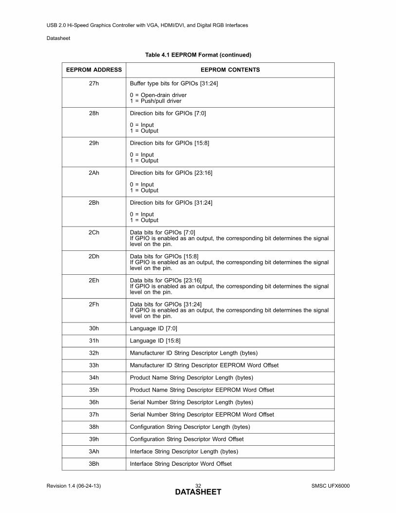
Note: Locations 4Ah and above may be used for any purpose.
Note 4.1 Refer to the software programming manual for information concerning this data structure.
Note 4.2 This block may include Binary Object Store (BOS) Descriptor, USB 2.0 ExtensionDescriptor, and Container ID Descriptor.
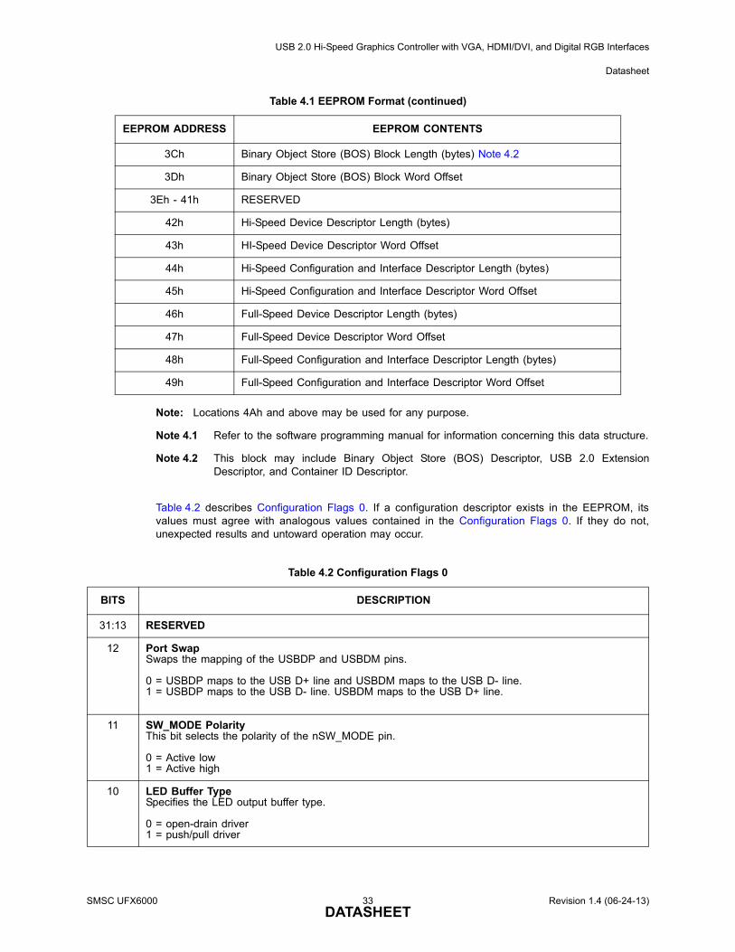
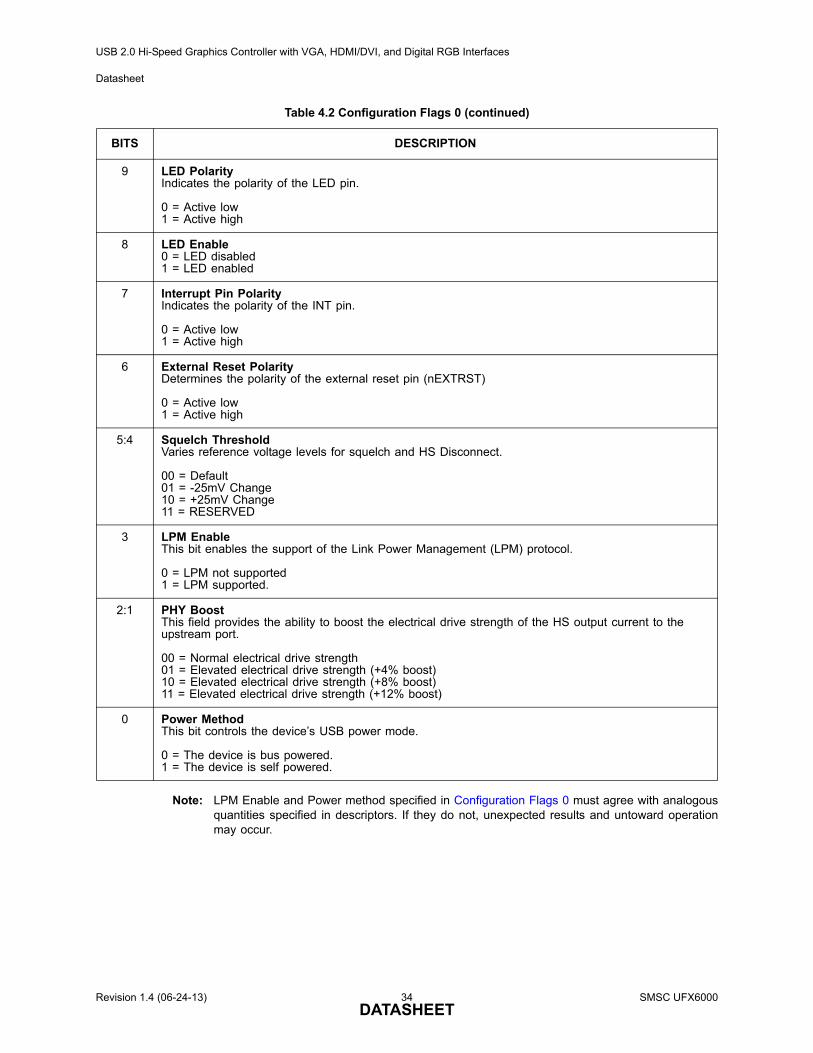
Table 4.2 describes Configuration Flags 0. If a configuration descriptor exists in the EEPROM, itsvalues must agree with analogous values contained in the Configuration Flags 0. If they do not,unexpected results and untoward operation may occur.
3Ch Binary Object Store (BOS) Block Length (bytes) Note 4.2
3Dh Binary Object Store (BOS) Block Word Offset
3Eh - 41h RESERVED
42h Hi-Speed Device Descriptor Length (bytes)
43h HI-Speed Device Descriptor Word Offset
44h Hi-Speed Configuration and Interface Descriptor Length (bytes)
45h Hi-Speed Configuration and Interface Descriptor Word Offset
46h Full-Speed Device Descriptor Length (bytes)
47h Full-Speed Device Descriptor Word Offset
48h Full-Speed Configuration and Interface Descriptor Length (bytes)
49h Full-Speed Configuration and Interface Descriptor Word Offset
Table 4.2 Configuration Flags 0
BITS DESCRIPTION
31:13 RESERVED
12 Port SwapSwaps the mapping of the USBDP and USBDM pins.
0 = USBDP maps to the USB D+ line and USBDM maps to the USB D- line.1 = USBDP maps to the USB D- line. USBDM maps to the USB D+ line.
11 SW_MODE PolarityThis bit selects the polarity of the nSW_MODE pin.
0 = Active low1 = Active high
10 LED Buffer TypeSpecifies the LED output buffer type.
0 = open-drain driver1 = push/pull driver
Table 4.1 EEPROM Format (continued)
EEPROM ADDRESS EEPROM CONTENTS
SMSC UFX6000 33 Revision 1.4 (06-24-13)DATASHEET
USB 2.0 Hi-Speed Graphics Controller with VGA, HDMI/DVI, and Digital RGB Interfaces
Datasheet
Note: LPM Enable and Power method specified in Configuration Flags 0 must agree with analogousquantities specified in descriptors. If they do not, unexpected results and untoward operationmay occur.
9 LED PolarityIndicates the polarity of the LED pin.
0 = Active low1 = Active high
8 LED Enable0 = LED disabled1 = LED enabled
7 Interrupt Pin PolarityIndicates the polarity of the INT pin.
0 = Active low1 = Active high
6 External Reset PolarityDetermines the polarity of the external reset pin (nEXTRST)
0 = Active low1 = Active high
5:4 Squelch ThresholdVaries reference voltage levels for squelch and HS Disconnect.
00 = Default01 = -25mV Change10 = +25mV Change11 = RESERVED
3 LPM EnableThis bit enables the support of the Link Power Management (LPM) protocol.
0 = LPM not supported1 = LPM supported.
2:1 PHY BoostThis field provides the ability to boost the electrical drive strength of the HS output current to the upstream port.
00 = Normal electrical drive strength01 = Elevated electrical drive strength (+4% boost)10 = Elevated electrical drive strength (+8% boost)11 = Elevated electrical drive strength (+12% boost)
0 Power MethodThis bit controls the device’s USB power mode.
0 = The device is bus powered.1 = The device is self powered.
Table 4.2 Configuration Flags 0 (continued)
BITS DESCRIPTION
Revision 1.4 (06-24-13) 34 SMSC UFX6000DATASHEET
USB 2.0 Hi-Speed Graphics Controller with VGA, HDMI/DVI, and Digital RGB Interfaces
Datasheet
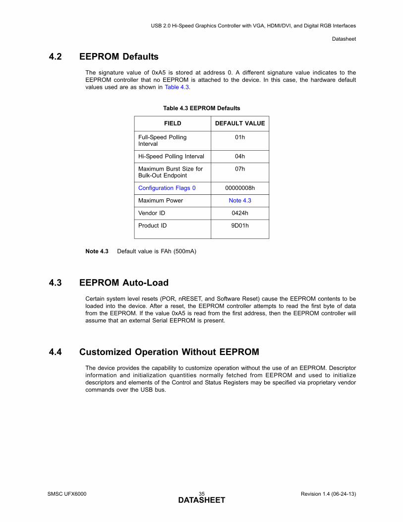
4.2 EEPROM Defaults
The signature value of 0xA5 is stored at address 0. A different signature value indicates to theEEPROM controller that no EEPROM is attached to the device. In this case, the hardware defaultvalues used are as shown in Table 4.3.
Note 4.3 Default value is FAh (500mA)
4.3 EEPROM Auto-Load
Certain system level resets (POR, nRESET, and Software Reset) cause the EEPROM contents to beloaded into the device. After a reset, the EEPROM controller attempts to read the first byte of datafrom the EEPROM. If the value 0xA5 is read from the first address, then the EEPROM controller willassume that an external Serial EEPROM is present.
4.4 Customized Operation Without EEPROM
The device provides the capability to customize operation without the use of an EEPROM. Descriptorinformation and initialization quantities normally fetched from EEPROM and used to initializedescriptors and elements of the Control and Status Registers may be specified via proprietary vendorcommands over the USB bus.
Table 4.3 EEPROM Defaults
FIELD DEFAULT VALUE
Full-Speed Polling Interval
01h
Hi-Speed Polling Interval 04h
Maximum Burst Size for Bulk-Out Endpoint
07h
Configuration Flags 0 00000008h
Maximum Power Note 4.3
Vendor ID 0424h
Product ID 9D01h
SMSC UFX6000 35 Revision 1.4 (06-24-13)DATASHEET
USB 2.0 Hi-Speed Graphics Controller with VGA, HDMI/DVI, and Digital RGB Interfaces
Datasheet
Chapter 5 Operational Characteristics
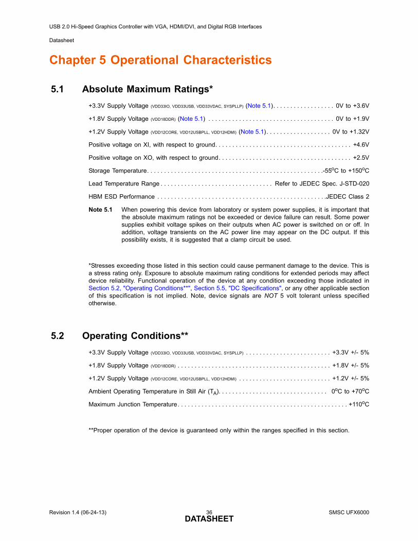
5.1 Absolute Maximum Ratings*
+3.3V Supply Voltage (VDD33IO, VDD33USB, VDD33VDAC, SYSPLLP) (Note 5.1). . . . . . . . . . . . . . . . . . 0V to +3.6V
+1.8V Supply Voltage (VDD18DDR) (Note 5.1) . . . . . . . . . . . . . . . . . . . . . . . . . . . . . . . . . . . . . 0V to +1.9V
+1.2V Supply Voltage (VDD12CORE, VDD12USBPLL, VDD12HDMI) (Note 5.1). . . . . . . . . . . . . . . . . . . 0V to +1.32V
Positive voltage on XI, with respect to ground. . . . . . . . . . . . . . . . . . . . . . . . . . . . . . . . . . . . . . . . +4.6V
Positive voltage on XO, with respect to ground. . . . . . . . . . . . . . . . . . . . . . . . . . . . . . . . . . . . . . . +2.5V
Storage Temperature. . . . . . . . . . . . . . . . . . . . . . . . . . . . . . . . . . . . . . . . . . . . . . . . . . . .-55oC to +150oC
Lead Temperature Range . . . . . . . . . . . . . . . . . . . . . . . . . . . . . . . . . Refer to JEDEC Spec. J-STD-020
HBM ESD Performance . . . . . . . . . . . . . . . . . . . . . . . . . . . . . . . . . . . . . . . . . . . . . . . . . .JEDEC Class 2
Note 5.1 When powering this device from laboratory or system power supplies, it is important thatthe absolute maximum ratings not be exceeded or device failure can result. Some powersupplies exhibit voltage spikes on their outputs when AC power is switched on or off. Inaddition, voltage transients on the AC power line may appear on the DC output. If thispossibility exists, it is suggested that a clamp circuit be used.
*Stresses exceeding those listed in this section could cause permanent damage to the device. This isa stress rating only. Exposure to absolute maximum rating conditions for extended periods may affectdevice reliability. Functional operation of the device at any condition exceeding those indicated inSection 5.2, "Operating Conditions**", Section 5.5, "DC Specifications", or any other applicable sectionof this specification is not implied. Note, device signals are NOT 5 volt tolerant unless specifiedotherwise.
5.2 Operating Conditions**
+3.3V Supply Voltage (VDD33IO, VDD33USB, VDD33VDAC, SYSPLLP) . . . . . . . . . . . . . . . . . . . . . . . . . +3.3V +/- 5%
+1.8V Supply Voltage (VDD18DDR) . . . . . . . . . . . . . . . . . . . . . . . . . . . . . . . . . . . . . . . . . . . . . +1.8V +/- 5%
+1.2V Supply Voltage (VDD12CORE, VDD12USBPLL, VDD12HDMI) . . . . . . . . . . . . . . . . . . . . . . . . . . . +1.2V +/- 5%
Ambient Operating Temperature in Still Air (TA). . . . . . . . . . . . . . . . . . . . . . . . . . . . . . . . 0oC to +70oC
Maximum Junction Temperature. . . . . . . . . . . . . . . . . . . . . . . . . . . . . . . . . . . . . . . . . . . . . . . . . . +110oC
**Proper operation of the device is guaranteed only within the ranges specified in this section.
Revision 1.4 (06-24-13) 36 SMSC UFX6000DATASHEET
USB 2.0 Hi-Speed Graphics Controller with VGA, HDMI/DVI, and Digital RGB Interfaces
Datasheet
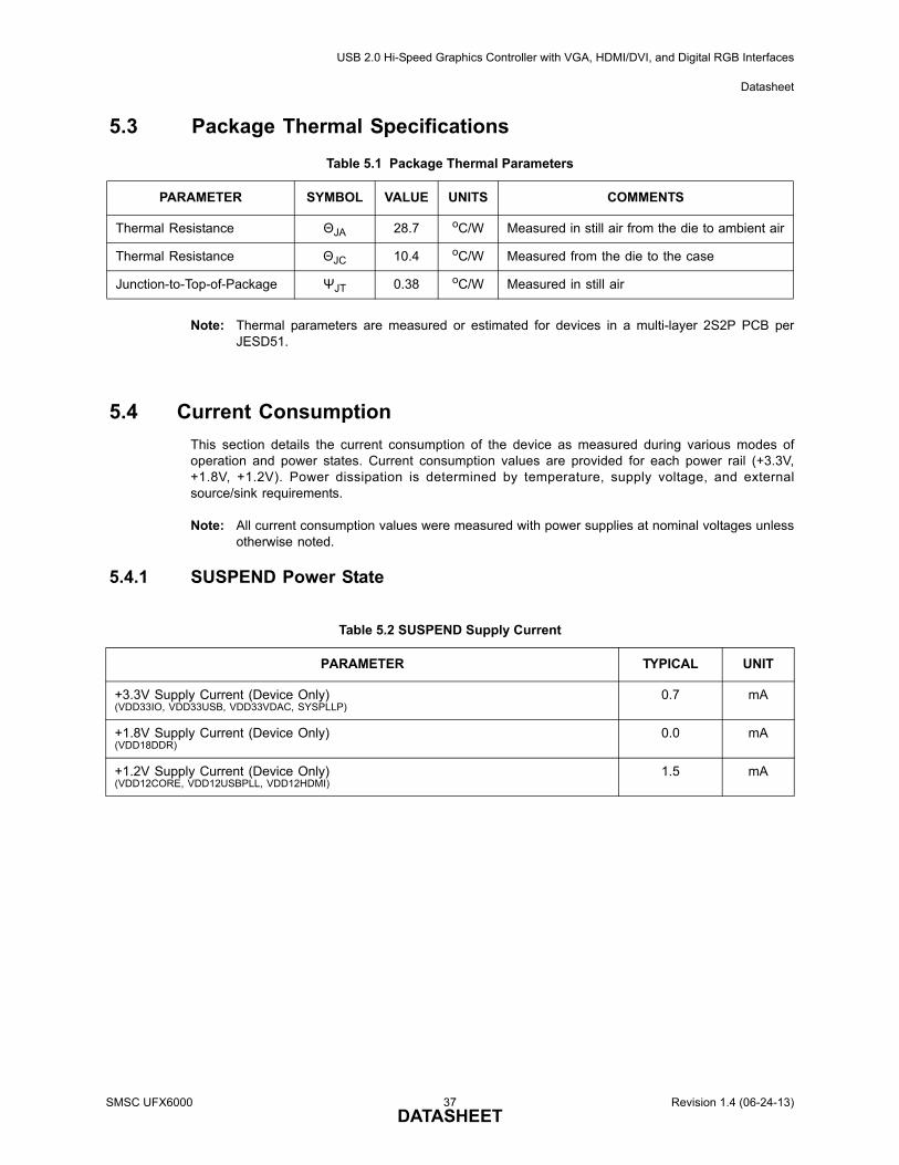
5.3 Package Thermal Specifications
Note: Thermal parameters are measured or estimated for devices in a multi-layer 2S2P PCB perJESD51.
5.4 Current Consumption
This section details the current consumption of the device as measured during various modes ofoperation and power states. Current consumption values are provided for each power rail (+3.3V,+1.8V, +1.2V). Power dissipation is determined by temperature, supply voltage, and externalsource/sink requirements.
Note: All current consumption values were measured with power supplies at nominal voltages unlessotherwise noted.
5.4.1 SUSPEND Power State
Table 5.1 Package Thermal Parameters
PARAMETER SYMBOL VALUE UNITS COMMENTS
Thermal Resistance ΘJA 28.7 oC/W Measured in still air from the die to ambient air
Thermal Resistance ΘJC 10.4 oC/W Measured from the die to the case
Junction-to-Top-of-Package ΨJT 0.38 oC/W Measured in still air
Table 5.2 SUSPEND Supply Current
PARAMETER TYPICAL UNIT
+3.3V Supply Current (Device Only)(VDD33IO, VDD33USB, VDD33VDAC, SYSPLLP)
0.7 mA
+1.8V Supply Current (Device Only)(VDD18DDR)
0.0 mA
+1.2V Supply Current (Device Only)(VDD12CORE, VDD12USBPLL, VDD12HDMI)
1.5 mA
SMSC UFX6000 37 Revision 1.4 (06-24-13)DATASHEET
USB 2.0 Hi-Speed Graphics Controller with VGA, HDMI/DVI, and Digital RGB Interfaces
Datasheet
5.4.2 Operational
5.4.2.1 High-Speed
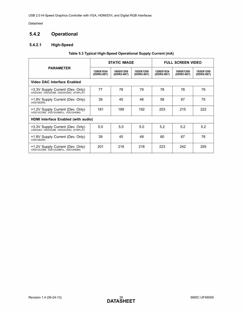
Table 5.3 Typical High-Speed Operational Supply Current (mA)
PARAMETER
STATIC IMAGE FULL SCREEN VIDEO
1280X1024(DDR2-667)
1600X1200(DDR2-667)
1920X1200(DDR2-667)
1280X1024(DDR2-667)
1600X1200(DDR2-667)
1920X1200(DDR2-667)
Video DAC Interface Enabled
+3.3V Supply Current (Dev. Only)(VDD33IO, VDD33USB, VDD33VDAC, SYSPLLP)
77 78 79 78 78 79
+1.8V Supply Current (Dev. Only)(VDD18DDR)
39 45 48 58 67 75
+1.2V Supply Current (Dev. Only)(VDD12CORE, VDD12USBPLL, VDD12HDMI)
181 189 192 203 215 222
HDMI Interface Enabled (with audio)
+3.3V Supply Current (Dev. Only)(VDD33IO, VDD33USB, VDD33VDAC, SYSPLLP)
5.0 5.0 5.0 5.2 5.2 5.2
+1.8V Supply Current (Dev. Only)(VDD18DDR)
39 45 49 60 67 76
+1.2V Supply Current (Dev. Only)(VDD12CORE, VDD12USBPLL, VDD12HDMI)
201 218 218 223 242 255
Revision 1.4 (06-24-13) 38 SMSC UFX6000DATASHEET
USB 2.0 Hi-Speed Graphics Controller with VGA, HDMI/DVI, and Digital RGB Interfaces
Datasheet
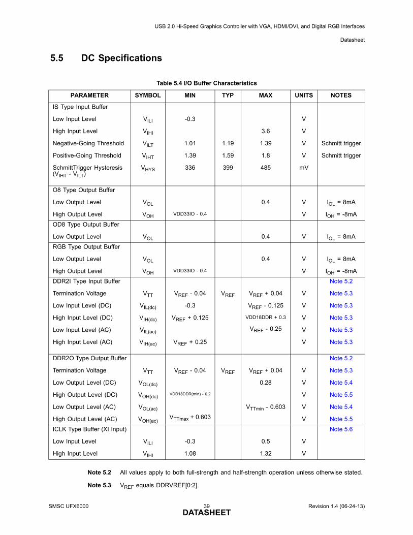
5.5 DC Specifications
Note 5.2 All values apply to both full-strength and half-strength operation unless otherwise stated.
Note 5.3 VREF equals DDRVREF[0:2].
Table 5.4 I/O Buffer Characteristics
PARAMETER SYMBOL MIN TYP MAX UNITS NOTES
IS Type Input Buffer
Low Input Level
High Input Level
Negative-Going Threshold
Positive-Going Threshold
SchmittTrigger Hysteresis (VIHT - VILT)
VILI
VIHI
VILT
VIHT
VHYS
-0.3
1.01
1.39
336
1.19
1.59
399
3.6
1.39
1.8
485
V
V
V
V
mV
Schmitt trigger
Schmitt trigger
O8 Type Output Buffer
Low Output Level
High Output Level
VOL
VOH VDD33IO - 0.4
0.4 V
V
IOL = 8mA
IOH = -8mA
OD8 Type Output Buffer
Low Output Level VOL 0.4 V IOL = 8mA
RGB Type Output Buffer
Low Output Level
High Output Level
VOL
VOH VDD33IO - 0.4
0.4 V
V
IOL = 8mA
IOH = -8mA
DDR2I Type Input Buffer
Termination Voltage
Low Input Level (DC)
High Input Level (DC)
Low Input Level (AC)
High Input Level (AC)
VTT
VIL(dc)
VIH(dc)
VIL(ac)
VIH(ac)
VREF - 0.04
-0.3
VREF + 0.125
VREF + 0.25
VREF VREF + 0.04
VREF - 0.125
VDD18DDR + 0.3
VREF - 0.25
V
V
V
V
V
Note 5.2
Note 5.3
Note 5.3
Note 5.3
Note 5.3
Note 5.3
DDR2O Type Output Buffer
Termination Voltage
Low Output Level (DC)
High Output Level (DC)
Low Output Level (AC)
High Output Level (AC)
VTT
VOL(dc)
VOH(dc)
VOL(ac)
VOH(ac)
VREF - 0.04
VDD18DDR(min) - 0.2
VTTmax + 0.603
VREF VREF + 0.04
0.28
VTTmin - 0.603
V
V
V
V
V
Note 5.2
Note 5.3
Note 5.4
Note 5.5
Note 5.4
Note 5.5
ICLK Type Buffer (XI Input)
Low Input Level
High Input Level
VILI
VIHI
-0.3
1.08
0.5
1.32
V
V
Note 5.6
SMSC UFX6000 39 Revision 1.4 (06-24-13)DATASHEET
USB 2.0 Hi-Speed Graphics Controller with VGA, HDMI/DVI, and Digital RGB Interfaces
Datasheet
Note 5.4 IOL equals 13.4mA for full-strength operation and 6.7mA for half-strength operation.
Note 5.5 IOH equals -13.4mA for full-strength operation and -6.7mA for half-strength operation.
Note 5.6 XI can optionally be driven from a 25MHz single-ended clock oscillator.
5.6 AC Specifications
This section details the various AC timing specifications of the device.
Note: The USB interface timing adheres to the USB 2.0 Specification. Refer to the Universal SerialBus Revision 2.0 Specification for detailed USB timing information.
Note: The DDR2 interface timing adheres to the JESD79-2E Specification. Refer to the JESD79-2ESpecification for detailed DDR2 timing information.
Note: The HDMI interface timing adheres to the HDMI 1.3 Specification. Refer to the HDMI 1.3Specification for detailed HDMI timing information.
Note: The S/PDIF interface timing adheres to the IEC 60958 2-channel PCM Specification. Refer tothe IEC 60958 2-channel PCM Specification for detailed S/PDIF timing information.
Note: The I2S interface timing adheres to the NXP I2S Bus Specification. Refer to the NXP I2S BusSpecification for detailed I2S timing information.
Note: The I2C interface timing adheres to the NXP I2C-Bus Specification. Refer to the I2C-BusSpecification for detailed I2C timing information.
Table 5.5 Video DAC - DC Characteristics
PARAMETER SYMBOL MIN TYP MAX UNITS
Output Voltage - 1.28 V
Output Current per Channel - 17 mA
Video DAC Resolution - 10 bits
Integral Non-linearity Error INL +/-2 LSB
Differential Non-linearity Error DNL +/-0.5 LSB
Revision 1.4 (06-24-13) 40 SMSC UFX6000DATASHEET
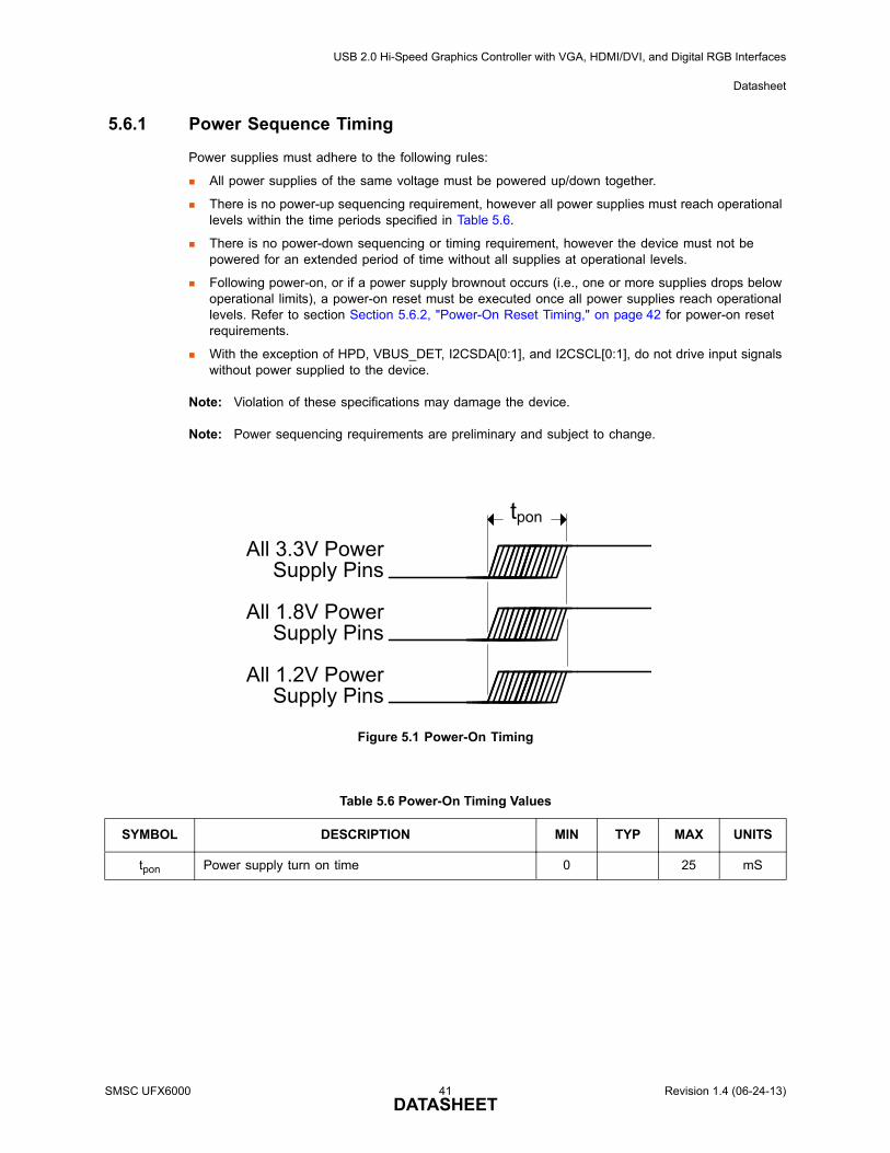
USB 2.0 Hi-Speed Graphics Controller with VGA, HDMI/DVI, and Digital RGB Interfaces
Datasheet
5.6.1 Power Sequence Timing
Power supplies must adhere to the following rules:
All power supplies of the same voltage must be powered up/down together.
There is no power-up sequencing requirement, however all power supplies must reach operational levels within the time periods specified in Table 5.6.
There is no power-down sequencing or timing requirement, however the device must not be powered for an extended period of time without all supplies at operational levels.
Following power-on, or if a power supply brownout occurs (i.e., one or more supplies drops below operational limits), a power-on reset must be executed once all power supplies reach operational levels. Refer to section Section 5.6.2, "Power-On Reset Timing," on page 42 for power-on reset requirements.
With the exception of HPD, VBUS_DET, I2CSDA[0:1], and I2CSCL[0:1], do not drive input signals without power supplied to the device.
Note: Violation of these specifications may damage the device.
Note: Power sequencing requirements are preliminary and subject to change.
Figure 5.1 Power-On Timing
Table 5.6 Power-On Timing Values
SYMBOL DESCRIPTION MIN TYP MAX UNITS
tpon Power supply turn on time 0 25 mS
All 3.3V Power Supply Pins
All 1.8V Power Supply Pins
All 1.2V Power Supply Pins
tpon
SMSC UFX6000 41 Revision 1.4 (06-24-13)DATASHEET
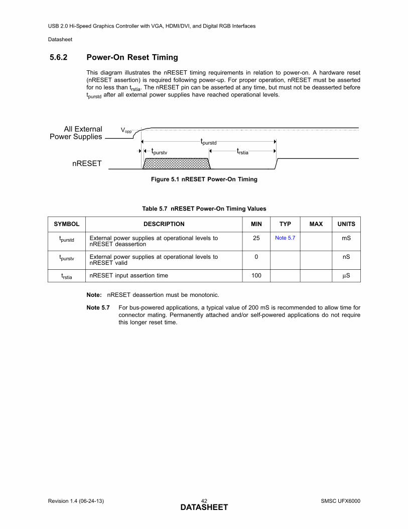
USB 2.0 Hi-Speed Graphics Controller with VGA, HDMI/DVI, and Digital RGB Interfaces
Datasheet
5.6.2 Power-On Reset Timing
This diagram illustrates the nRESET timing requirements in relation to power-on. A hardware reset(nRESET assertion) is required following power-up. For proper operation, nRESET must be assertedfor no less than trstia. The nRESET pin can be asserted at any time, but must not be deasserted beforetpurstd after all external power supplies have reached operational levels.
Note: nRESET deassertion must be monotonic.
Note 5.7 For bus-powered applications, a typical value of 200 mS is recommended to allow time forconnector mating. Permanently attached and/or self-powered applications do not requirethis longer reset time.
Figure 5.1 nRESET Power-On Timing
Table 5.7 nRESET Power-On Timing Values
SYMBOL DESCRIPTION MIN TYP MAX UNITS
tpurstd External power supplies at operational levels to nRESET deassertion
25 Note 5.7 mS
tpurstv External power supplies at operational levels to nRESET valid
0 nS
trstia nRESET input assertion time 100 μS
nRESET
trstia
All External Power Supplies
tpurstd
Vopp
tpurstv
Revision 1.4 (06-24-13) 42 SMSC UFX6000DATASHEET
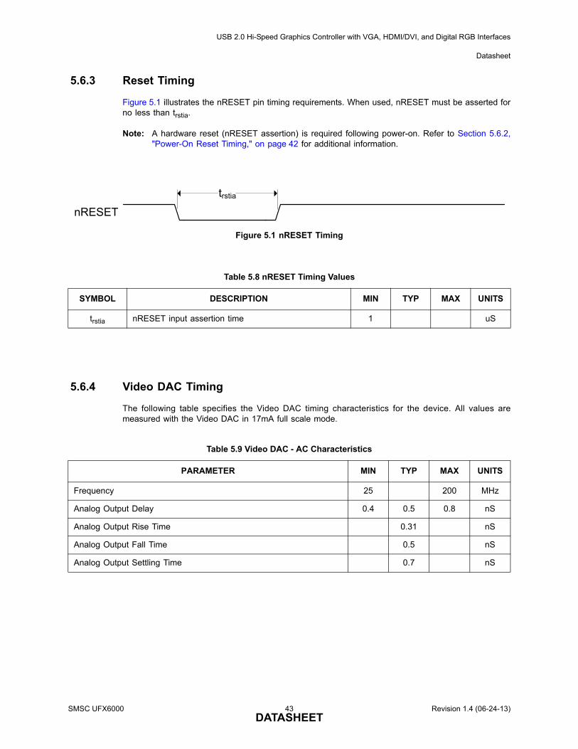
USB 2.0 Hi-Speed Graphics Controller with VGA, HDMI/DVI, and Digital RGB Interfaces
Datasheet
5.6.3 Reset Timing
Figure 5.1 illustrates the nRESET pin timing requirements. When used, nRESET must be asserted forno less than trstia.
Note: A hardware reset (nRESET assertion) is required following power-on. Refer to Section 5.6.2,"Power-On Reset Timing," on page 42 for additional information.
5.6.4 Video DAC Timing
The following table specifies the Video DAC timing characteristics for the device. All values aremeasured with the Video DAC in 17mA full scale mode.
Figure 5.1 nRESET Timing
Table 5.8 nRESET Timing Values
SYMBOL DESCRIPTION MIN TYP MAX UNITS
trstia nRESET input assertion time 1 uS
Table 5.9 Video DAC - AC Characteristics
PARAMETER MIN TYP MAX UNITS
Frequency 25 200 MHz
Analog Output Delay 0.4 0.5 0.8 nS
Analog Output Rise Time 0.31 nS
Analog Output Fall Time 0.5 nS
Analog Output Settling Time 0.7 nS
nRESET
trstia
SMSC UFX6000 43 Revision 1.4 (06-24-13)DATASHEET
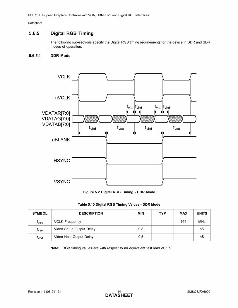
USB 2.0 Hi-Speed Graphics Controller with VGA, HDMI/DVI, and Digital RGB Interfaces
Datasheet
5.6.5 Digital RGB Timing
The following sub-sections specify the Digital RGB timing requirements for the device in DDR and SDRmodes of operation.
5.6.5.1 DDR Mode
Note: RGB timing values are with respect to an equivalent test load of 5 pF.
Figure 5.2 Digital RGB Timing - DDR Mode
Table 5.10 Digital RGB Timing Values - DDR Mode
SYMBOL DESCRIPTION MIN TYP MAX UNITS
fvclk VCLK Frequency 165 MHz
tvsu Video Setup Output Delay 0.8 nS
tvhd Video Hold Output Delay 0.5 nS
VDATAR[7:0]VDATAG[7:0]VDATAB[7:0]
nBLANK
tvhdtvsu
HSYNC
VSYNC
tvsutvhd
VCLK
nVCLK
tvhd
tvhdtvsu
tvsu
Revision 1.4 (06-24-13) 44 SMSC UFX6000DATASHEET
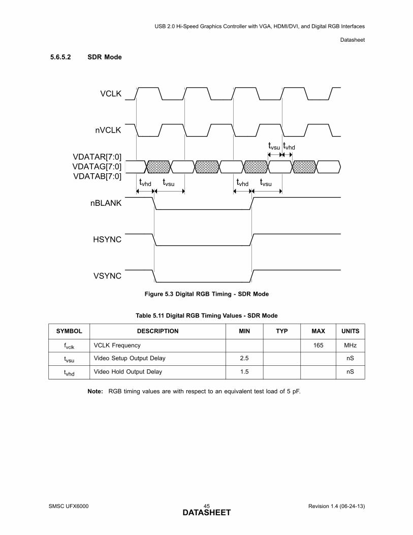
USB 2.0 Hi-Speed Graphics Controller with VGA, HDMI/DVI, and Digital RGB Interfaces
Datasheet
5.6.5.2 SDR Mode
Note: RGB timing values are with respect to an equivalent test load of 5 pF.
Figure 5.3 Digital RGB Timing - SDR Mode
Table 5.11 Digital RGB Timing Values - SDR Mode
SYMBOL DESCRIPTION MIN TYP MAX UNITS
fvclk VCLK Frequency 165 MHz
tvsu Video Setup Output Delay 2.5 nS
tvhd Video Hold Output Delay 1.5 nS
VCLK
VDATAR[7:0]VDATAG[7:0]VDATAB[7:0]
nBLANK
tvhdtvsu
HSYNC
VSYNC
tvsu
nVCLK
tvhd tvsutvhd
SMSC UFX6000 45 Revision 1.4 (06-24-13)DATASHEET
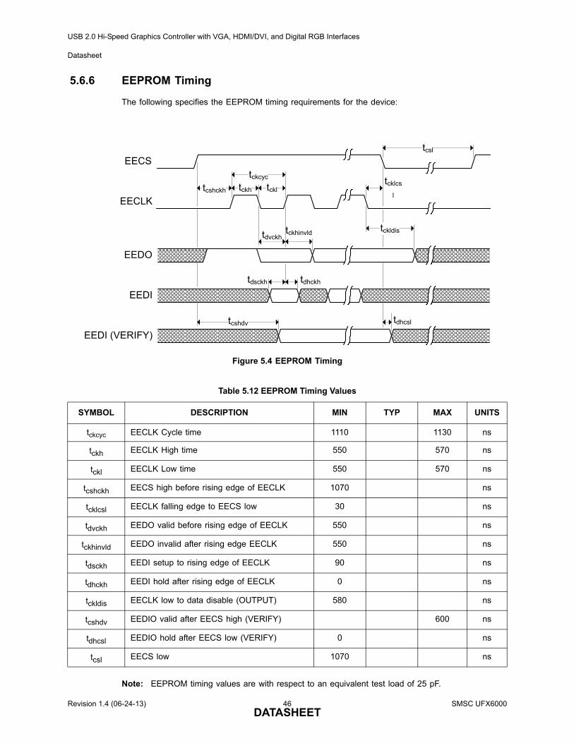
USB 2.0 Hi-Speed Graphics Controller with VGA, HDMI/DVI, and Digital RGB Interfaces
Datasheet
5.6.6 EEPROM Timing
The following specifies the EEPROM timing requirements for the device:
Note: EEPROM timing values are with respect to an equivalent test load of 25 pF.
Figure 5.4 EEPROM Timing
Table 5.12 EEPROM Timing Values
SYMBOL DESCRIPTION MIN TYP MAX UNITS
tckcyc EECLK Cycle time 1110 1130 ns
tckh EECLK High time 550 570 ns
tckl EECLK Low time 550 570 ns
tcshckh EECS high before rising edge of EECLK 1070 ns
tcklcsl EECLK falling edge to EECS low 30 ns
tdvckh EEDO valid before rising edge of EECLK 550 ns
tckhinvld EEDO invalid after rising edge EECLK 550 ns
tdsckh EEDI setup to rising edge of EECLK 90 ns
tdhckh EEDI hold after rising edge of EECLK 0 ns
tckldis EECLK low to data disable (OUTPUT) 580 ns
tcshdv EEDIO valid after EECS high (VERIFY) 600 ns
tdhcsl EEDIO hold after EECS low (VERIFY) 0 ns
tcsl EECS low 1070 ns
EECLK
EEDO
EEDI
EECS
tckldis
tcshckh
EEDI (VERIFY)
tckh tckl
tckcyc tcklcs
l
tcsl
tdvckhtckhinvld
tdsckh tdhckh
tdhcsltcshdv
Revision 1.4 (06-24-13) 46 SMSC UFX6000DATASHEET
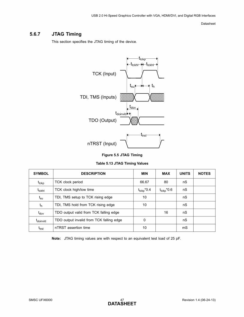
USB 2.0 Hi-Speed Graphics Controller with VGA, HDMI/DVI, and Digital RGB Interfaces
Datasheet
5.6.7 JTAG Timing
This section specifies the JTAG timing of the device.
Note: JTAG timing values are with respect to an equivalent test load of 25 pF.
Figure 5.5 JTAG Timing
Table 5.13 JTAG Timing Values
SYMBOL DESCRIPTION MIN MAX UNITS NOTES
ttckp TCK clock period 66.67 80 nS
ttckhl TCK clock high/low time ttckp*0.4 ttckp*0.6 nS
tsu TDI, TMS setup to TCK rising edge 10 nS
th TDI, TMS hold from TCK rising edge 10 nS
tdov TDO output valid from TCK falling edge 16 nS
tdoinvld TDO output invalid from TCK falling edge 0 nS
ttrst nTRST assertion time 10 mS
TCK (Input)
TDI, TMS (Inputs)
ttckhl
ttckp
ttckhl
tsu th
tdov
TDO (Output)
tdoinvld
ttrst
nTRST (Input)
SMSC UFX6000 47 Revision 1.4 (06-24-13)DATASHEET
USB 2.0 Hi-Speed Graphics Controller with VGA, HDMI/DVI, and Digital RGB Interfaces
Datasheet
5.7 Clock Circuit
The device can accept either a 25MHz crystal or a 25MHz single-ended clock oscillator (+/- 50ppm)input. If the single-ended clock oscillator method is implemented, XO should be left unconnected andXI should be driven with a nominal 0-1.2V clock signal. The input clock duty cycle is 40% minimum,50% typical and 60% maximum.
It is recommended that a crystal utilizing matching parallel load capacitors be used for the crystalinput/output signals (XI/XO). See Table 5.14 for the recommended crystal specifications.
Note 5.8 The maximum allowable values for Frequency Tolerance and Frequency Stability areapplication dependant.
Note 5.9 Frequency Deviation Over Time is also referred to as Aging.
Note 5.10 This number includes the pad, the bond wire and the lead frame. PCB capacitance is notincluded in this value. The XO/XI pin and PCB capacitance values are required toaccurately calculate the value of the two external load capacitors. These two external loadcapacitors determine the accuracy of the 25.000 MHz frequency.
Table 5.14 Crystal Specifications
PARAMETER SYMBOL MIN NOM MAX UNITS NOTES
Crystal Cut AT, typ
Crystal Oscillation Mode Fundamental Mode
Crystal Calibration Mode Parallel Resonant Mode
Frequency Ffund - 25.000 - MHz
Frequency Tolerance @ 25oC Ftol - - +/-50 PPM Note 5.8
Frequency Stability Over Temp Ftemp - - +/-100 PPM Note 5.8
Frequency Deviation Over Time Fage - +/-3 to 5 - PPM Note 5.9
Total Allowable PPM Budget - - +/-150 PPM
Shunt Capacitance CO - 7 typ - pF
Load Capacitance CL - 20 typ - pF
Drive Level PW 300 - - uW
Equivalent Series Resistance R1 - - 50 Ohm
Operating Temperature Range 0 - 70 oC
XI Pin Capacitance - 3 typ - pF Note 5.10
XO Pin Capacitance - 3 typ - pF Note 5.10
Revision 1.4 (06-24-13) 48 SMSC UFX6000DATASHEET
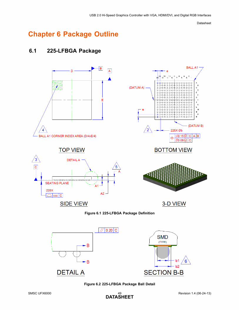
USB 2.0 Hi-Speed Graphics Controller with VGA, HDMI/DVI, and Digital RGB Interfaces
Datasheet
Chapter 6 Package Outline
6.1 225-LFBGA Package
Figure 6.1 225-LFBGA Package Definition
Figure 6.2 225-LFBGA Package Ball Detail
SMSC UFX6000 49 Revision 1.4 (06-24-13)DATASHEET
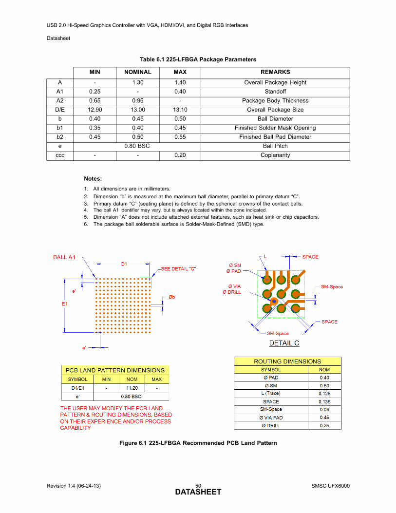
USB 2.0 Hi-Speed Graphics Controller with VGA, HDMI/DVI, and Digital RGB Interfaces
Datasheet
Notes:
1. All dimensions are in millimeters.
2. Dimension “b” is measured at the maximum ball diameter, parallel to primary datum “C”.3. Primary datum “C” (seating plane) is defined by the spherical crowns of the contact balls.4. The ball A1 identifier may vary, but is always located within the zone indicated.
5. Dimension “A” does not include attached external features, such as heat sink or chip capacitors.6. The package ball solderable surface is Solder-Mask-Defined (SMD) type.
Table 6.1 225-LFBGA Package Parameters
MIN NOMINAL MAX REMARKS
A - 1.30 1.40 Overall Package Height
A1 0.25 - 0.40 Standoff
A2 0.65 0.96 - Package Body Thickness
D/E 12.90 13.00 13.10 Overall Package Size
b 0.40 0.45 0.50 Ball Diameter
b1 0.35 0.40 0.45 Finished Solder Mask Opening
b2 0.45 0.50 0.55 Finished Ball Pad Diameter
e 0.80 BSC Ball Pitch
ccc - - 0.20 Coplanarity
Figure 6.1 225-LFBGA Recommended PCB Land Pattern
Revision 1.4 (06-24-13) 50 SMSC UFX6000DATASHEET
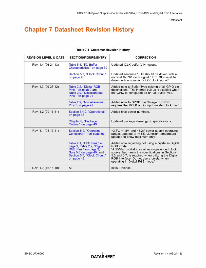
USB 2.0 Hi-Speed Graphics Controller with VGA, HDMI/DVI, and Digital RGB Interfaces
Datasheet
SMSC UFX6000 51 Revision 1.4 (06-24-13)DATASHEET
Chapter 7 Datasheet Revision History
Table 7.1 Customer Revision History
REVISION LEVEL & DATE SECTION/FIGURE/ENTRY CORRECTION
Rev. 1.4 (06-24-13) Table 5.4, “I/O Buffer Characteristics,” on page 39
Updated ICLK buffer VIHI values.
Section 5.7, "Clock Circuit," on page 48
Updated sentence “...XI should be driven with a nominal 0-3.3V clock signal.” to “...XI should be driven with a nominal 0-1.2V clock signal”.
Rev. 1.3 (09-27-12) Table 2.2, “Digital RGB Pins,” on page 9 and Table 2.9, “Miscellaneous Pins,” on page 21
Added note to Buffer Type column of all GPIO pin descriptions: “The internal pull-up is disabled when the GPIO is configured as an O8 buffer type.”
Table 2.9, “Miscellaneous Pins,” on page 21
Added note to SPDIF pin “Usage of SPDIF requires the MCLK audio input master clock pin.”
Rev. 1.2 (09-16-11) Section 5.4.2, "Operational," on page 38
Added final power numbers.
Chapter 6, "Package Outline," on page 49
Updated package drawings & specifications.
Rev. 1.1 (05-13-11) Section 5.2, "Operating Conditions**," on page 36
+3.3V, +1.8V, and +1.2V power supply operating ranges updated to +/-5%. Junction temperature updated to show maximum only.
Table 2.1, “USB Pins,” on page 9, Table 2.2, “Digital RGB Pins,” on page 9, Note 5.6 on page 40, and Section 5.7, "Clock Circuit," on page 48
Added note regarding not using a crystal in Digital RGB mode:“A 25Mhz oscillator, or other single ended clock source that meets the specifications in Sections 5.5 and 5.7, is required when utilizing the Digital RGB interface. Do not use a crystal when operating in Digital RGB mode.”
Rev. 1.0 (12-16-10) All Initial Release