Embed Size (px)
Citation preview
UNIVERSITY OF TARTU
FACULTY OF SCIENCE AND TECHNOLOGY
INSTITUTE OF TECHNOLOGY
Jaanus Kalde
UHF COMMUNICATION SYSTEM FOR
CUBESATELLITE
Master's thesis (30 EAP)
Supervisors:
Assistant professor Mart Noorma
MSc Viljo Allik
Tartu 2015
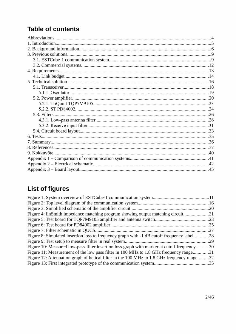
Table of contentsAbbreviations...................................................................................................................................41. Introduction..................................................................................................................................52. Background information...............................................................................................................63. Previous solutions.........................................................................................................................9
3.1. ESTCube-1 communication system.....................................................................................93.2. Commercial systems...........................................................................................................12
4. Requirements..............................................................................................................................134.1. Link budget.........................................................................................................................14
5. Technical solution.......................................................................................................................165.1. Transceiver..........................................................................................................................18
5.1.1. Oscillator.....................................................................................................................195.2. Power amplifier..................................................................................................................20
5.2.1. TriQuint TQP7M9105.................................................................................................235.2.2. ST PD84002................................................................................................................24
5.3. Filters..................................................................................................................................264.3.1. Low-pass antenna filter...............................................................................................265.3.2. Receive input filter......................................................................................................31
5.4. Circuit board layout............................................................................................................336. Tests............................................................................................................................................357. Summary....................................................................................................................................368. References..................................................................................................................................379. Kokkuvõte..................................................................................................................................40Appendix 1 – Comparison of communication systems..................................................................41Appendix 2 – Electrical schematic.................................................................................................42Appendix 3 – Board layout............................................................................................................45
List of figuresFigure 1: System overview of ESTCube-1 communication system...............................................11Figure 2: Top level diagram of the communication system...........................................................16Figure 3: Simplified schematic of the amplifier circuit..................................................................20Figure 4: linSmith impedance matching program showing output matching circuit.....................21Figure 5: Test board for TQP7M9105 amplifier and antenna switch.............................................23Figure 6: Test board for PD84002 amplifier..................................................................................25Figure 7: Filter schematic in QUCS...............................................................................................27Figure 8: Simulated insertion loss to frequency graph with -1 dB cutoff frequency label............28Figure 9: Test setup to measure filter in real system......................................................................29Figure 10: Measured low-pass filter insertion loss graph with marker at cutoff frequency...........30Figure 11: Measurement of the low pass filter in 100 MHz to 1.8 GHz frequency range.............31Figure 12: Attenuation graph of helical filter in the 100 MHz to 1.8 GHz frequency range.........32Figure 13: First integrated prototype of the communication system..............................................35
2/46
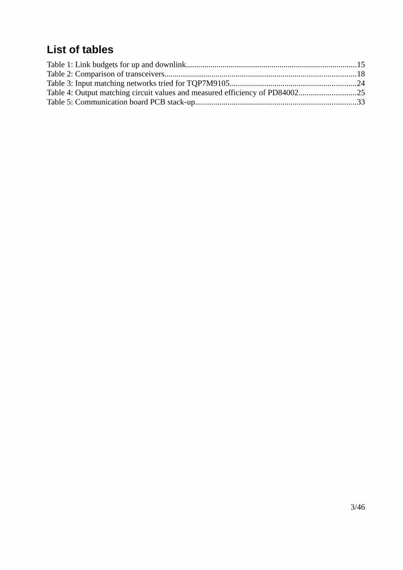
List of tablesTable 1: Link budgets for up and downlink....................................................................................15Table 2: Comparison of transceivers..............................................................................................18Table 3: Input matching networks tried for TQP7M9105..............................................................24Table 4: Output matching circuit values and measured efficiency of PD84002............................25Table 5: Communication board PCB stack-up...............................................................................33
3/46
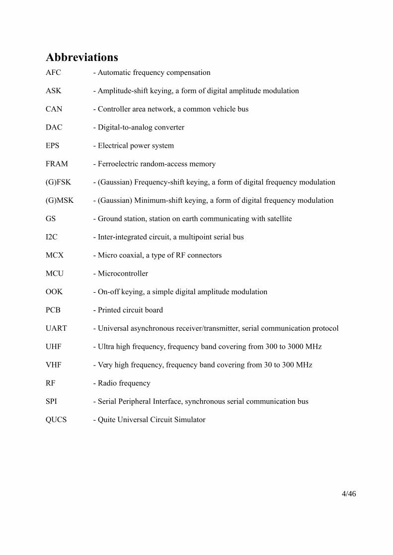
AbbreviationsAFC - Automatic frequency compensation
ASK - Amplitude-shift keying, a form of digital amplitude modulation
CAN - Controller area network, a common vehicle bus
DAC - Digital-to-analog converter
EPS - Electrical power system
FRAM - Ferroelectric random-access memory
(G)FSK - (Gaussian) Frequency-shift keying, a form of digital frequency modulation
(G)MSK - (Gaussian) Minimum-shift keying, a form of digital frequency modulation
GS - Ground station, station on earth communicating with satellite
I2C - Inter-integrated circuit, a multipoint serial bus
MCX - Micro coaxial, a type of RF connectors
MCU - Microcontroller
OOK - On-off keying, a simple digital amplitude modulation
PCB - Printed circuit board
UART - Universal asynchronous receiver/transmitter, serial communication protocol
UHF - Ultra high frequency, frequency band covering from 300 to 3000 MHz
VHF - Very high frequency, frequency band covering from 30 to 300 MHz
RF - Radio frequency
SPI - Serial Peripheral Interface, synchronous serial communication bus
QUCS - Quite Universal Circuit Simulator
4/46
1. IntroductionThis masters thesis covers design and prototyping of a ultra high frequency communication
system for CubeSats. Design is based on the requirements set by Estonian next proposed satellite
ESTCube-2.
CubeSat is a small satellite standard that is widely used for research and educational purposes.
Most satellites need a way to communicate with Earth to allow sending commands to the satellite
and receiving telemetry and mission data.
The goal of this thesis is to design and prototype a communication system suitable for CubeSats.
It covers calculating link budgets, deciding the system architecture, choosing and testing all
required components and designing first integrated prototype. Communication system has to be
designed to work in space environment and meet all the needed requirements. Space and
CubeSats have numerous design limitations, especially in size and energy usage.
5/46
2. Background informationCubeSat is a miniaturized picosatellite standard. CubeSat standard defines base satellite unit(U)
with 10 cm x 10 cm x 10 cm size and up to 1.3 kg weight [1]. From the base unit size there are
defined multiple satellite sizes like 2 U, 3 U, 6 U etc. Launching and mechanical construction is
standardized for CubeSats. This makes them much cheaper and easier to launch to orbit than
regular satellites. Standard subsystems have created a market for components - thus lowering
price and furthering innovation. Such tiny picosatellites are mainly used for education and
component testing. European Space Agency, NASA [2] and several universities have their
educational CubeSat programs. Most widely known such program in Estonia is probably
Estonian Student Satellite Program program.
There are also companies that use these miniature CubeSats instead of big satellites to provide
services for their clients. For example American company Planet Labs, whose satellite
constellations Flocks use three unit CubeSats called Doves, to provide real time visible spectrum
imaging of planet Earth [3].
ESTCube-1 was first Estonian satellite - built by students with its main purpose being education.
It was 1 U CubeSat, with main scientific goal to test electric solar wind sail [4]. Electric solar
wind sail is a novel proposed space propulsion method. Like other solar wind sail propulsion
methods - it works by deflecting plasma originating from the sun. These kinds of propulsion
methods are low thrust. But their major advantage is that they do not require propellant, thus
providing acceleration times limited only by spacecraft lifetime. This allows building light and
small spacecraft with big manoeuvring capabilities. Electric solar wind sail one type of solar
wind sail. It uses one or multiple tethers, charged to a high voltage potential to generate electric
field. This electric field is used as a sail surface to provide force.
ESTCube-2 is a planned satellite to test out solar wind sail in low Earth orbit. The mission needs
a communication subsystem to transmit commands to the satellite and download experiment data
to ground stations on the ground. Mission details are not yet fixed at the moment, but basic
requirements to develop communication system have been agreed on. It will be a low Earth orbit
satellite with altitude in the order of magnitude of 350 km.
Electronic systems in Earth orbit are in different environment than normal Earth systems. One of
the biggest difference is accessibility - once the satellite is in orbit it cannot be repaired
6/46
physically. Second important difference is the lack of atmosphere. It changes thermal
management as heat transfer by convection is no longer available. It also has other effects. It
produces stress to all closed containers. Also many plastics and similar materials release gases in
vacuum that may contaminate optics and other sensors. From mechanical standpoint the launch
to the orbit is the most important. All satellite components must survive vibrations and shocks
that come from launching the satellite with rocket.
One of the limiting aspects of CubeSats is their size and weight. Very small size of the whole
satellite puts limits on the size on the subsystems. Many satellites use PC/104 mechanical form
factor – 90 mm x 96 mm sized cards stacked on top of each other. Subsystems are divided
between the cards and communicate through stack connector. Very limited size also means
limited surface area – which in turn, little power generation. On ESTCube-1 power generation
during sunlight was between 2.4 to 3.4 W. This very little power means that all subsystems have
to be as efficient and low power as possible. This kind of power budget limits power available for
communication and payloads [5].
One of the most important aspect of any communication system terrestrial or orbital is the
operating frequency band. Electromagnetic spectrum is a finite and global resource. It is very
important topic to satellites because satellites can transmit above many different countries and the
signal cannot interfere any other application. Global frequency allocation is done by International
Telecommunication Union and allocating frequency band can take more than five years and can
be costly. Since most CubeSats are built on limited time scale and budget many of the
educational and scientific ones use radio amateur frequencies. Getting an allocated radio amateur
frequency from governing International Amateur Radio Union easier progress, but has its own
requirements. All communication on the amateur bands must be non-encrypted and documented
publicly.
For wireless communication modulation is also an important aspect. Modulation defines the way
information is encoded to radio signals [20]. The most simple modulation is on-off keying –
turning carrier frequency on and off. This modulation is not very robust, but is used in amateur
radio for sending low speed Morse coded signals. This was used in ESTCube-1 safe mode
beacon to provide basic telemetry information, that would be simple to receive and decode.
Frequency-shift keying is widely used digital modulation. It decodes information to change of the
frequency. The most simple version of it – binary frequency-shift keying (BFSK/2FSK)
7/46
modulation uses two different frequencies, where one frequency means digital one and another a
digital zero. It is also possible to use more than two frequencies – for example QFSK uses four.
Space communication differs from terrestrial communication in several ways. The most
challenging aspect about it is the distance. Satellites in low Earth orbit are between 300 to 1000
km above the surface of the planet. This means that free space loss in the communication path is
substantial. At higher frequencies atmospheric losses also play a role. High speed that the satellite
is moving causes Doppler effect. Transmitting frequency received from the ground station is
changing according to the speed of the satellite compared to listener. Big telecommunication
satellites have built in Doppler correction. For small satellites this compensation is made in
ground station.
To still have good connection with satellite even after these losses the ground stations for
satellites usually have high gain parabolic or Yagi antennas and use high power for transmitting.
These antennas point towards the satellite the whole communication time. Some aspects of the
communications are easier compared to terrestrial. Terrestrial communications usually have
reflection and losses from other objects on the ground. Space communications usually have line
of sight communications with no additional losses or reflections. This allows the use of simple
narrow band modulations instead of more complex multipath ones.
Many of the radio measurements made in this work were done with Hewlett-Packard 4396A
network analyser. Network analyser is a radio measuring device that combines spectrum analyser
and tracking generator. Spectrum analyser allows to measure and plot radio spectrum in one
frequency range. Tracking generator adds functionality to do more complex measurements like
insertion loss and phase shift measurements over a frequency range and measuring reflected RF
power and phase shift do determine input matching.
8/46
3. Previous solutionsCommunication system designed for this thesis work is a based on ESTCube-1 communication
subsystem. This subsystem is working successfully on the orbit and is used for telemetry and
image data transfer. It was designed by Andres an Toomas Vahter.
Before designing this system commercial systems were considered and researched to provide
comparison to ESTCube-1 and new solutions.
3.1. ESTCube-1 communication systemESTCube-1 communications system is a half duplex system that uses different frequency bands
for uplink and downlink. System architecture and connections between components are shown in
figure 1 [18]. For downlink 9600 baud 430 MHz UHF frequency was used. Maximum output
power for downlink is 0.5 W / 27 dBm. For uplink - 1200 baud 143 MHz VHF [7]. Both links are
fixed baud and use 2FSK modulation with 25 kHz bandwidth. System also had separate 0.1 W /
20 dBm OOK Morse beacon downlink that is directly controlled by power system to provide
backup communication channel.
Transmit and receive circuits had separate ADF7021 transceivers. Separate Morse beacon was
generated with Silicon Labs Si570 programmable crystal oscillator. Downlink was amplified to
necessary level with programmable gain power amplifier RFPA0133. Receiving input has RFMD
SGL0363Z low noise amplifier with theoretical noise figure of 1.1 dB [13]. Both channels had
separate antenna connectors so there was no need for RF switching. Transmit circuit had the
ability to measure transmitted and reflected RF power using directional couplers and logarithmic
amplifiers.
ESTCube-1 used two monopole antennas. Monopole antennas were used because their ease of
construction and since they are omnidirectional. Scientific mission required satellite to spin and
still have a communication link. This determined the use of omnidirectional antenna.
9/46

10/46
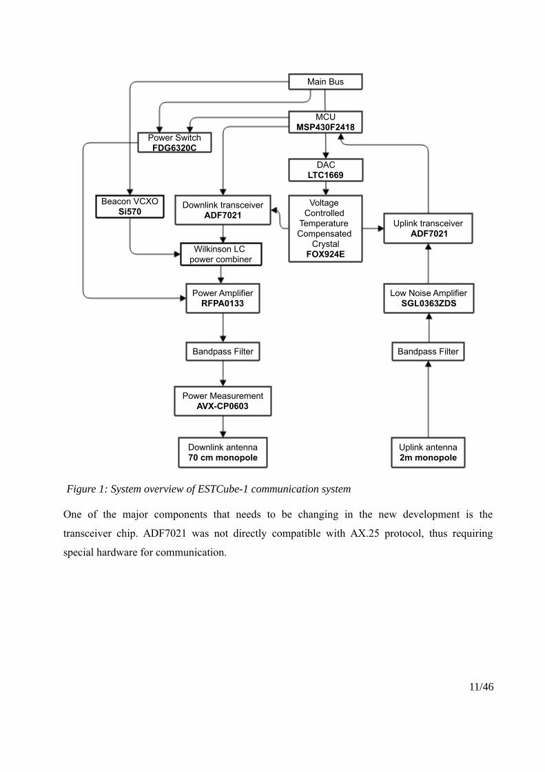
One of the major components that needs to be changing in the new development is the
transceiver chip. ADF7021 was not directly compatible with AX.25 protocol, thus requiring
special hardware for communication.
11/46
Figure 1: System overview of ESTCube-1 communication system
Main Bus
MCUMSP430F2418
Downlink transceiverADF7021
VoltageControlled
TemperatureCompensated
CrystalFOX924E
DACLTC1669
Power MeasurementAVX-CP0603
Power SwitchFDG6320C
Low Noise AmplifierSGL0363ZDS
Uplink transceiver ADF7021
Power AmplifierRFPA0133
Bandpass Filter
Downlink antenna70 cm monopole
Bandpass Filter
Uplink antenna2m monopole
Beacon VCXOSi570
Wilkinson LCpower combiner
3.2. Commercial systemsA list of four commercial transceivers were considered as a reference. GomSpace NanoCom
AX1000 and U482C, Clyde Space UTRX and ISIS Full Duplex Transceiver. Full comparison
table is in the appendix 1. All of the commercial modules supported speeds from 1200 to 9600
with AX100 supporting up to 115200 bps transmit speeds. All modules used I2C with AX100
being the only one to support a fault tolerant industrial communication bus – CAN. The AX100
module was only system that was not compilable with PC/104, but offered support board that
makes is possible to combine the module and one more module on one PC/104 card.
None of the communication systems were designed to be very efficient – for all of the systems
less than half of the power consumed during transmit goes to RF output. From modulation
standpoint – two of the four systems offered constant wave beacon output, three of the systems
had FSK modulation and only supported had phase shift keying (PSK) modulation. FSK
modulation is more widely used in narrow band applications, although PSK offers better data
rates for same signal to noise ratio.
12/46
4. RequirementsFor the finished system there are several top level requirements. It has to conform with
ESTCube-2 technical requirements: power, voltages, internal communication and mechanical.
Also – in order to commercialise this as a product after development it has to provide better value
than existing commercial systems on the market.
ESTCube-2 system bus sets numerous requirements that the communication system has to
comply.
• Mechanical layout has to match required dimensions and have necessary fixing holes
• System bus has to have specific connector specified with correct pinout
• System has to use available voltages – 3.3 V, 5 V, 12 V, unregulated 8 V.
• System is required to have two independent RS-485 buses.
• Main microcontroller (MCU) has to be same as in other subsystems to maximize code
portability
It also has several radio requirements it has to comply:
• International Amateur Radio Union rules allow satellite communication multiple
frequency ranges. Two way ultra high frequency communication is allowed in the
frequency range 435-438 MHz [6].
• It has to provide 1 W / 30 dBm of RF power output to antenna
• It has to have OOK modulation output capability for safe mode beacon
• System has to have two-way binary Gaussian frequency-shift keying (2GFSK)
communications
• Has to have standard AX.25 9600 baud radio amateur mode
• Provide changeable on air baud rates from 9600 to 38400 bps
13/46
4.1. Link budgetLink budgets are used to calculate different aspects of communication systems. Link budget
accounts of all aspects of the telecommunication link. It consists of transmitter parameters, losses
in the transmitter, transmitting medium and receiver. It also incorporates receiver parameters and
and link data rate [19]. It is used to find theoretical maximum data rate of a link. For a given bit
rate it is also possible to calculate link margin that gives indication of robustness of the
communication.
First part of the calculation is calculating transmitter Equivalent Isotropic Radiated Power (EIRP)
– metric of radiated power from the antenna. Second part of the calculation consists of
calculating all transmission and receiving losses. Then it is possible to calculate signal to noise
ratio for current bit rates. Finally link margin can be calculated.
Formula used to calculate EIRP is:
EIRP = PT – LT + GT
Where PT is transmission power, LT is transmission loss and GT is transmitter antenna gain.
Then propagation losses are calculated:
Lprop = FSL + Labs
Where Labs is atmospheric absorption and FSL is free space loss what is calculated:
FSL=(4 πd f
c)
2
=20 log10(d)+20 log10( f )−147.55
Formula to calculate received power from the antenna is:
Pr*G = EIRP – Lprop + G
Where G is receive antenna gain, Lprop is propagation losses and EIRP is equivalent isotropic
radiated power.
Last step is to calculate received signal to noise ratio per bit:
Eb/N0 = Pr*G – 10 log(rb) – k – 10 log(Ts)
Where Boltzmann constant k = -198,6 dBm/K, Ts is system noise temperature and rb is bit rate.
14/46
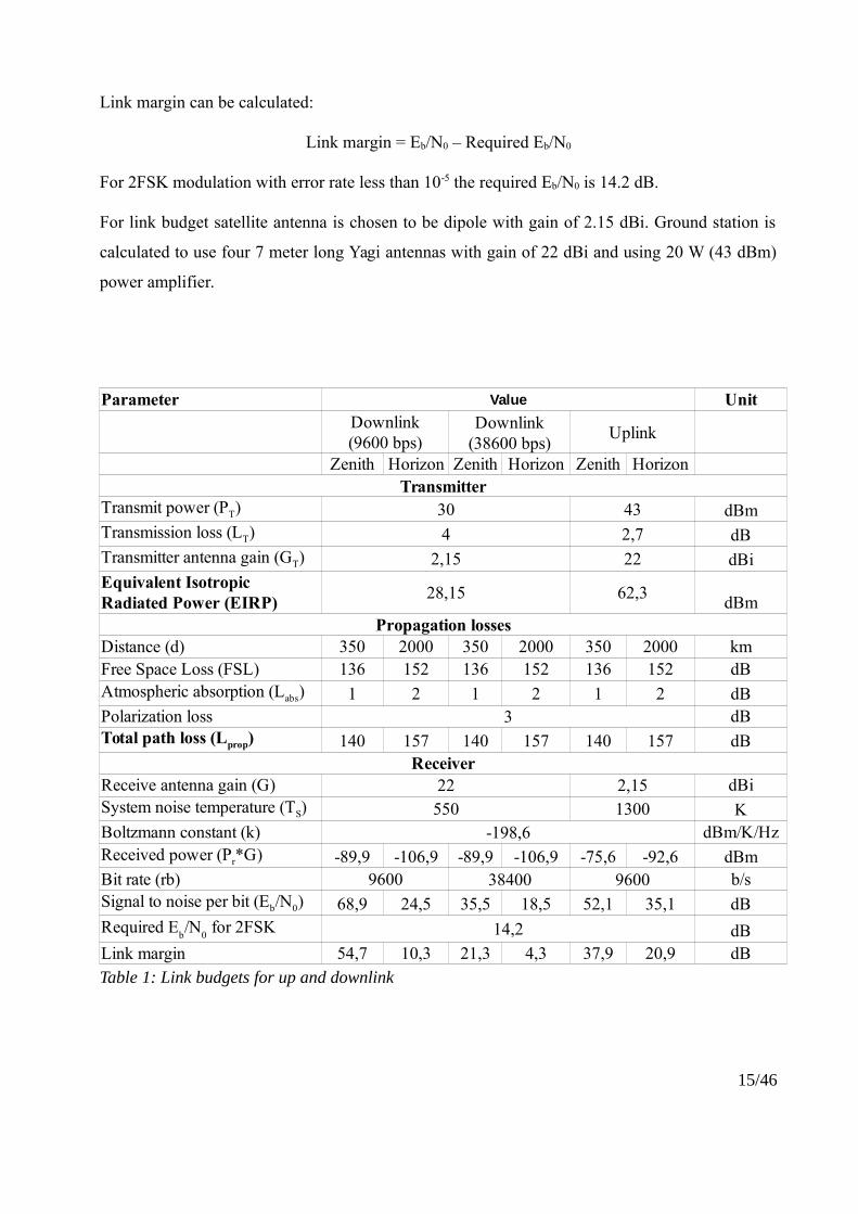
Link margin can be calculated:
Link margin = Eb/N0 – Required Eb/N0
For 2FSK modulation with error rate less than 10-5 the required Eb/N0 is 14.2 dB.
For link budget satellite antenna is chosen to be dipole with gain of 2.15 dBi. Ground station is
calculated to use four 7 meter long Yagi antennas with gain of 22 dBi and using 20 W (43 dBm)
power amplifier.
Table 1: Link budgets for up and downlink
15/46
Parameter Value Unit
Uplink
Zenith Horizon Zenith Horizon Zenith HorizonTransmitter
30 43 dBm4 2,7 dB
2,15 22 dBi
28,15 62,3dBm
Propagation lossesDistance (d) 350 2000 350 2000 350 2000 kmFree Space Loss (FSL) 136 152 136 152 136 152 dB
1 2 1 2 1 2 dBPolarization loss 3 dB
140 157 140 157 140 157 dBReceiver
Receive antenna gain (G) 22 2,15 dBi
550 1300 KBoltzmann constant (k) -198,6 dBm/K/Hz
-89,9 -106,9 -89,9 -106,9 -75,6 -92,6 dBmBit rate (rb) 9600 38400 9600 b/s
68,9 24,5 35,5 18,5 52,1 35,1 dB
14,2 dBLink margin 54,7 10,3 21,3 4,3 37,9 20,9 dB
Downlink(9600 bps)
Downlink(38600 bps)
Transmit power (PT)
Transmission loss (LT)
Transmitter antenna gain (GT)
Equivalent IsotropicRadiated Power (EIRP)
Atmospheric absorption (Labs)
Total path loss (Lprop)
System noise temperature (TS)
Received power (Pr*G)
Signal to noise per bit (Eb/N0)
Required Eb/N
0 for 2FSK

5. Technical solutionMain components that have to be in
such system are microcontroller to
control the system and handle
packets, transceiver to convert data
to radio frequency (RF) signals and
back and power amplifier to boost
signal to level necessary to reach
earth.
Main bus connector provides power
and communication lines for the
system. 3.3 V and unregulated 8 V
lines are available from Electrical
power unit (EPS). For
communication with rest of the
satellite, two RS-485 interfaces are
available from the main bus.
Between microcontroller and main
bus there are two RS-485 interface
transceivers to convert main
communication interfaces to UART.
Microcontroller controls all of the other components of the subsystem, communicates with other
subsystems and decodes and buffers packets sent from ground station. Texas Instruments
MSP430FR5969 was chosen as the microcontroller. It is a microcontroller based on low power
and radiation tolerant ferroelectric random-access memory (FRAM) [8]. This microcontroller
was the biggest in the FRAM MCU product line at the time and EPS uses the same controller.
This microcontroller has two UART lines that can be used to satisfy double RS-485 requirement.
Besides these two lines it also has a separate hardware SPI line that is used to communicate with
transceiver, digital-to-analog converter and serial FRAM. This serial FRAM is used to store
firmware images for bootloader support.
16/46
Figure 2: Top level diagram of the communication system.
Main bus
MCU
Tranciever
Poweramplifier
Antennaswitch
Antenna
Powerswitch
Voltage controlledcrystal oscillator
Thermalsensor
Thermalsensor
Low passfilter
Powermeasurement
Helicalfilter
Radio frequency transceiver is set up by MCU to transmit and receive necessary RF signals.
Stable clock to the transceiver comes from temperature compensated voltage controlled crystal
oscillator. It is an crystal oscillator that outputs clipped sine wave. The oscillator is temperature
compensated to make it more stable in changing temperature environment. Oscillator voltage
control input is controlled by main microcontroller via digital-to-analog converter (DAC) to
provide frequency tuning by command.
Transceiver has separate receive and transmit pins that are connected to different signal paths.
Receive path is connected to antenna switch through band-pass filter. Transmitted signal goes
through power amplifier to boost its strength to necessary levels. Power amplifier temperature is
monitored, power can be switched and gain is controllable via DAC. Power amplifier output goes
through two way power measurement to antenna switch. Power measurement circuit measures
output and reflected power levels.
Antenna switch switches between transmit and receive signal paths. Between switch and antenna
connector there is a low-pass filter for crude filtering. For attaching antenna cable there is a MCX
connector.
The microcontroller is programmed in Code Composer Studio environment and programmed
using Texas Instruments tool MSP-FET430UIF. The code is written in C and divided between
different files per functionality to allow code reuse.
Antenna switch was chosen to be TriQuint TQP4M0010. It was chosen because of its availability,
low insertion loss and easy to use 50 Ohm matched inputs and outputs [22]. Low insertion loss is
important both for receive and transmit. For transmit – losses between amplifier and antenna
mean that amplifier has to transmit more power and the system becomes less efficient. For
receive insertion losses also have a bad effect – all losses between antenna and first amplifier
increase system noise temperature.
There is also a Fairchild Semiconductor FPF2700 power switch between power bus and power
amplifier. This power switch is used to turn off the power for the amplifier when not transmitting.
This feature is necessary, because power amplifier consumes similar amount of energy
irrespective to the state – amplifying or not.
17/46
5.1. TransceiverOne of the main components in communication system design is choosing transceiver. For this
different ultra high frequency transceiver integrated circuits were research and compiled to a big
comparison table. Short excerpt of this table, showing most important parameters is provided in
table 2.
Transceiver Modulations Output power (dBm) Sensitivity (dBm)
ADF7021 2..4FSK, MSK 13 -116
SI4438 (G)FSK, (G)FSK, OOK 20 -115
Si4455 (G)FSK 13 -115
Si446x (G)FSK, 4(G)FSK, MSK, OOK 20 -126
Si10xx FSK, GFSK, OOK 13/20 -121
SX1231H FSK, GFSK, MSK, GMSK, OOK 20 -114
MRF49XA FSK 7 -110
MAX7032 ASK, OOK, FSK 10 -107Table 2: Comparison of transceivers
Out of the eight suitable components put in the table Silicon Labs Si4463 was chosen for the
system. It was one of the components that allowed using FSK and OOK modulations. It was
stocked and available from multiple distributors. From the suitable components it had the best
sensitivity and high output power. High sensitivity allows not to use low noise amplifier in the
receive path – thus simplifying the system. High output power makes driving output power
amplifier easier. Si446x series chips are also used in HopeRF FSK modules, that have example
code for many different platforms.
The transceiver has some other features that make it suitable for uses. Data rate can be from 100
bps to 1 Mbps [21], satisfying the baud rate requirement. It also has built in automatic frequency
compensation (AFC) that allows to implement automatic Doppler shift correction. Automatic
frequency compensation allows to measure how much does the received signal deviate from
nominal signal because of Doppler shift. Then the communication system can compensate its
own transmit frequency, thus eliminating need to do Doppler shift compensation on the ground
station.
18/46
5.1.1. Oscillator
Temperature compensated voltage controlled crystal oscillator is used for precise frequency
generation. Crystal oscillators consist of quartz crystal and amplification circuitry. Oscillators
require power and output desired frequency. Crystal oscillator used in this circuit is a 26 MHz
clipped sine wave oscillator. Oscillator temperature compensation means that outside temperature
changes are internally compensated to provide more stable output frequency over the temperature
range. Oscillator has a feature that allows to change the frequency by changing analog input
voltage. This input voltage is connected to DAC to provide frequency fine tuning on command.
19/46
5.2. Power amplifierPower amplifier is a very important part of the communication system. It is the part that
consumes the most energy in an communication system and sometimes – in the whole satellite.
For the communication system two different amplifiers were tested: TriQuint TQP7M9105 and
ST PD84002. Both were chosen because they were available, had enough output power and they
work in required ultra high frequency range. Both amplifiers were in an industry standard SOT-
89 package. Amplifier used on ESTCube-1 RFMD RFPA0133 was not considered since it had
poor availability and sensitivity to mismatched loads.
For both amplifiers similar steps were done. First the amplifier was simulated in linSmith to
determine matching network. Then a development board was designed, soldered and measured
with network analyser. Finally necessary changes were made in the components to get the
performance needed.
Both of these amplifiers were basic FET transistors with some built in circuitry. Most of the
20/46
Figure 3: Simplified schematic of the amplifier circuit
components needed to make a functioning amplifier was external. They both functioned as a
class B amplifier with theoretical maximum of 78.5% efficiency. To make class B amplifier
several different external part are required as seen in figure 3. Input RF signal has to be AC
coupled and matched with amplifier input. Input also has to be DC biased to adjust amplification.
Output of the transistor has to be feed with power DC line and RF output has to be AC coupled
and matched with next circuit elements.
With RF components matching is important. Component matching means using reactive circuits
to match output impedances with next component input impedance. It is important to minimize
losses in the system. Typically RF systems, amplifier and antenna complex impedances are
matched to match 50 Ω purely resistive system.
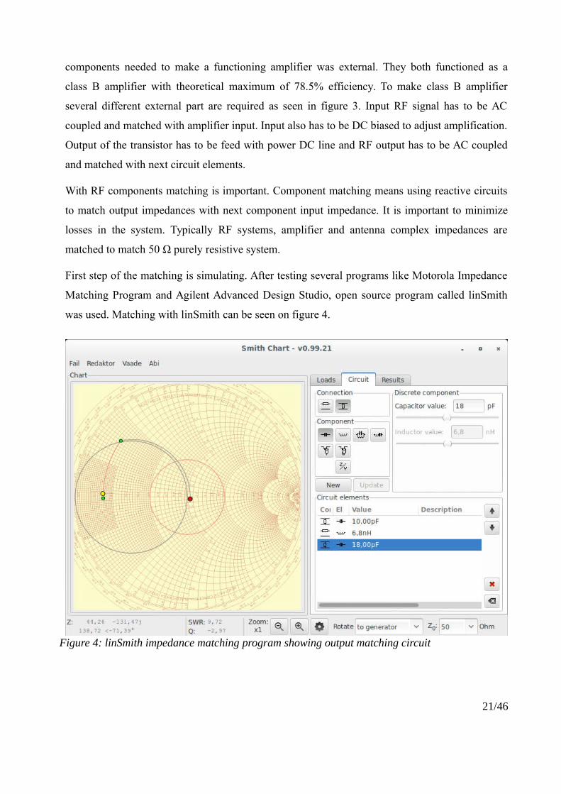
First step of the matching is simulating. After testing several programs like Motorola Impedance
Matching Program and Agilent Advanced Design Studio, open source program called linSmith
was used. Matching with linSmith can be seen on figure 4.
21/46
Figure 4: linSmith impedance matching program showing output matching circuit
Complex impedance and usable frequencies must be entered to the loads tab and then the circuit
can be described in the circuit tab. For input and output third order pi matching was used
consisting of capacitor to the ground, series inductor and second capacitor to the ground. Inductor
value was fixed, since inductors are available in less different values. Then capacitor values were
changed until input or output matched 50 Ω.
In the left of the window a Smitch chart of the circuit can be seen. Smitch chart shows complex
impedances on a logarithmic polar graph that makes different impedances visually
understandable. The centre line on the graph is the real axis with 50 Ω in the very centre. In the
left side there is 0 Ω resistance and on the right – open circuit.
LinSmith accepts complex impedance as an input, but both amplifiers provided only scattering
parameters (S parameters) in dB and angle format. Python and scikit-rf library were used to
convert these values from one representation to another. S parameters were provided for different
frequencies and for all combinations of two port amplifier. For input matching S11 parameter
was considered and for output matching S22. S11 describes impedance of first port in regard of
the first port, S22 second port in regard of the second port.
To convert from S parameters to complex impedance, first the values were saved in a Touchstone
SnP Format file. Example for one amplifier was following:
# MHz S DB R50
400 -2.73 176.91
The script that was used to convert this file to complex impedance was following
import skrf as rf
amp = rf.Network('amp.s1p')
print amp.z
Complex impedance output from this conversion was used in linSmith to calculate matching
networks. After calculating necessary matching components both amplifier boards were built up
and measured with network analyser.
DC power was provided according to datasheet values.
Input matching determines how much of the radio power going into the input of the amplifier is
actually amplified. It is not critical as long as power amplifier receives enough power. Input
22/46
matching was measured in two ways – measuring the change of the gain of the device. Bigger
gain means less losses in input matching. Second way the of measuring was to measure complex
RF power reflecting back from the input. Power is reflecting back means that input is not
matched well and knowing the complex impedance helps to determine necessary components.
Measuring output matching is more complicated than measuring input. Input complex impedance
can be measured with network analyser S11 measurement. Measurement gives out information
about mismatch and phase shift, that can be used to tweak the matching component values.
Measuring output matching of an amplifier can only be done indirectly – by measuring
amplification and efficiency of the amplifier. For both amplifiers pi matching network was used
and capacitor values were changed to get better efficiency and gain.
Since network analyser used could not provide enough power to drive the input of the power
amplifier a signal generator was used to provide constant wave test signal. Output of the
amplifier was measured with spectrum analyser to determine gain at centre frequency.
5.2.1. TriQuint TQP7M9105
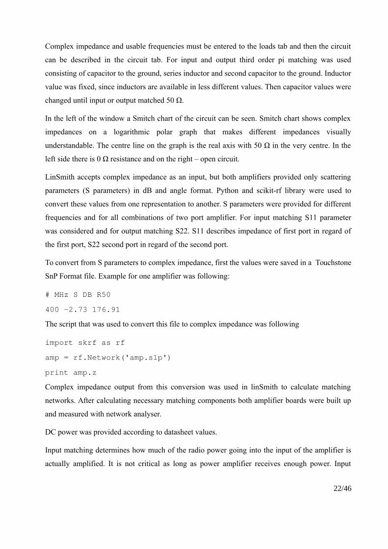
TriQuint TQP7M9105 is a 1 W high linearity amplifier [23]. This was the first amplifier that we
tested. It used 5 V line for DC power. Input impedance matching network was a L network with a
series inductor and parallel capacitor.
23/46
Figure 5: Test board for TQP7M9105 amplifier and antenna switch
Different component values were tried and impedances measured that are provided in table 3.
Inductor value (nH) Capacitor value (pF) S11 impedance measured (Ω)
1 0 4.1 + 8,7i
3.3 0 4.4 +14.5i
3.3 22 39 - 17i
3.3 18 47.3 + 8,7i
3.3 19 50 + 0,8i
Table 3: Input matching networks tried for TQP7M9105
For output many matching circuit configurations were tested. The best efficiency that was
achived was 29 dBm RF output with 2.5 W DC power draw. Efficiency for these values would be
0.8 W / 2.5 W = 32 %.
It turned out that this amplifier was meant to be high linearity amplifier, used in mobile telephone
base stations where efficiency is not a primary concern. Since this amplifier could not be used to
build a high efficiency power amplifier, a new amplifier was chosen.
5.2.2. ST PD84002
ST PD84002 was chosen because it provides up to 2 W output power in the necessary frequency
range. It also provides good efficiency. Test schematic and setup was very similar to previous
tested transistor. This transistor required 8 V power line instead of 5 V like previous. Because 8 V
line is available from ESTCube-2 system bus, the communication system does not need any local
regulation.
A prototype board was built up to test the amplifier. Prototype board can be seen in figure 6.
Inputs and outputs were AC coupled on the board with 100 pF ceramic capacitors. These
capacitors have so big capacitance that in ultra high frequency range their series resistance does
not affect matching circuits.
24/46
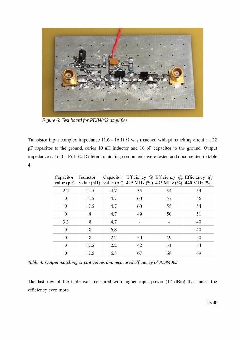
Transistor input complex impedance 11.6 - 16.1i Ω was matched with pi matching circuit: a 22
pF capacitor to the ground, series 10 nH inductor and 10 pF capacitor to the ground. Output
impedance is 16.0 - 16.1i Ω. Different matching components were tested and documented to table
4.
Capacitorvalue (pF)
Inductorvalue (nH)
Capacitorvalue (pF)
Efficiency @425 MHz (%)
Efficiency @433 MHz (%)
Efficiency @440 MHz (%)
2.2 12.5 4.7 55 54 54
0 12.5 4.7 60 57 56
0 17.5 4.7 60 55 54
0 8 4.7 49 50 51
3.3 8 4.7 - - 40
0 8 6.8 40
0 8 2.2 50 49 50
0 12.5 2.2 42 51 54
0 12.5 6.8 67 68 69
Table 4: Output matching circuit values and measured efficiency of PD84002
The last row of the table was measured with higher input power (17 dBm) that raised the
efficiency even more.
25/46
Figure 6: Test board for PD84002 amplifier
5.3. FiltersThere are two mayor RF filters in the system: low-pass antenna filter, band-pass receive input.
Filters for radio frequencies are different from regular analog filters – they are built only from
reactive components thus do not convert energy to heat. Most similar filters to typical RC filters
are lumped filters - RF filters that use inductors and capacitors as a circuit elements. Low pass
antenna filter is a lumped element filter in this system.
Designing a RF filter requires simulation, measurement in real system and tweaking of the
values. Simulation results show filter parameters and required components. Simulations are
important to determine component values and performance. Measurements of the built up system
can differ from the simulations, because of parasitic elements of the components. At high
frequencies component imperfections start to change the behaviour of the circuit. Inductors have
measurable resistances and capacitances. Capacitors have series inductances etc. The layout on
the circuit board can be important – inductors can couple with each other and ground planes
increase component capacitance.
4.3.1. Low-pass antenna filter
Between antenna switch and antenna connector there is an antenna filter. This is a low-pass filter,
which has to suppress spurious emissions generated by components on the signal path –
transceiver, power amplifier and antenna switch [9]. Low-pass filter has to have low insertion
loss, since it is in the high power patch.
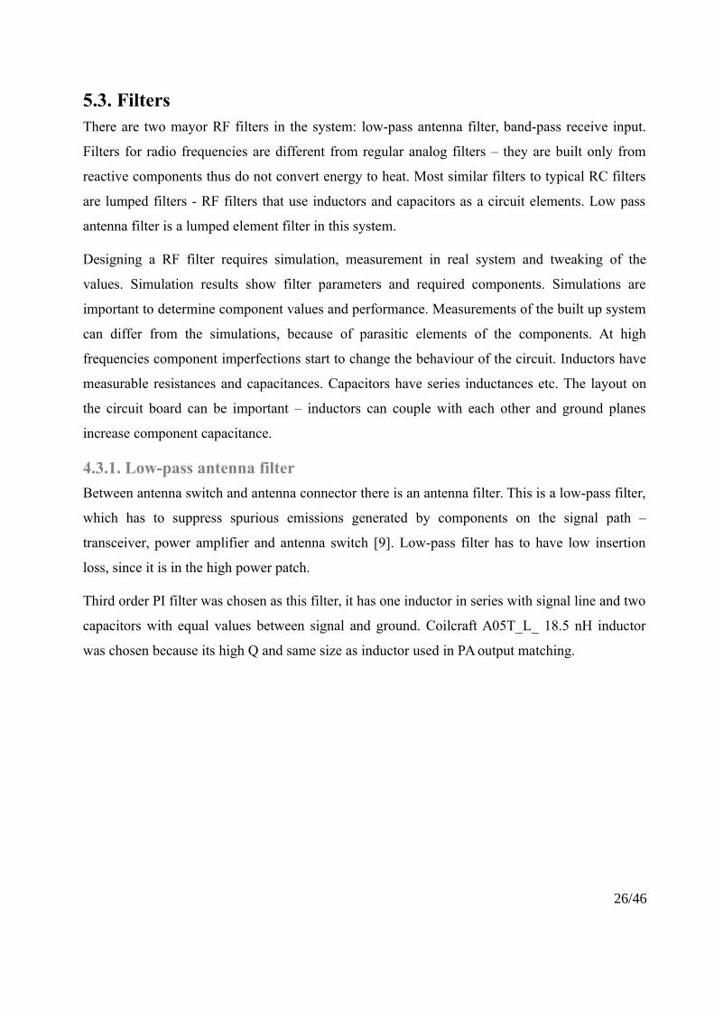
Third order PI filter was chosen as this filter, it has one inductor in series with signal line and two
capacitors with equal values between signal and ground. Coilcraft A05T_L_ 18.5 nH inductor
was chosen because its high Q and same size as inductor used in PA output matching.
26/46
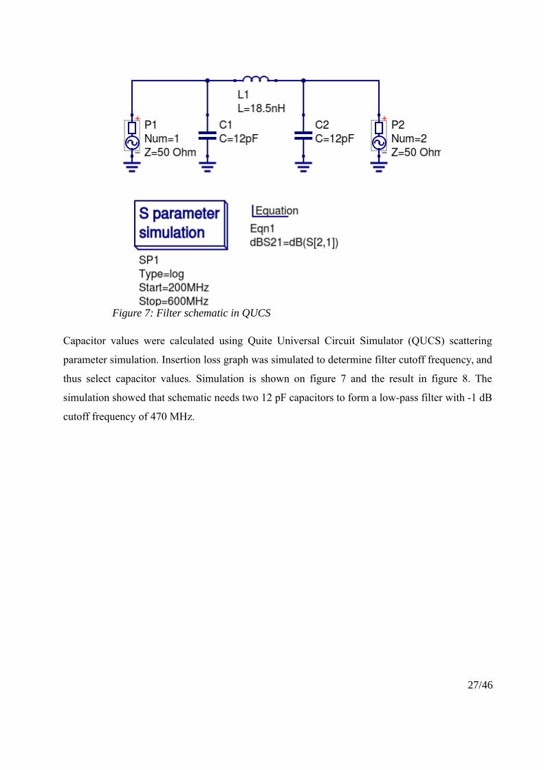
Figure 7: Filter schematic in QUCS
Capacitor values were calculated using Quite Universal Circuit Simulator (QUCS) scattering
parameter simulation. Insertion loss graph was simulated to determine filter cutoff frequency, and
thus select capacitor values. Simulation is shown on figure 7 and the result in figure 8. The
simulation showed that schematic needs two 12 pF capacitors to form a low-pass filter with -1 dB
cutoff frequency of 470 MHz.
27/46
Figure 8: Simulated insertion loss to frequency graph with -1 dB cutoff frequency label
Because of circuit board capacitance and component parasitic elements the real measured values
will differ from the simulated. To determine capacitor values that would be used in the real
system the filter was measured in the final circuit. Filter insertion losses were measured with
network analyser using antenna connector as one port and soldered coaxial cable as other.
Network analyser was configured to measure S12 – insertion loss.
28/46
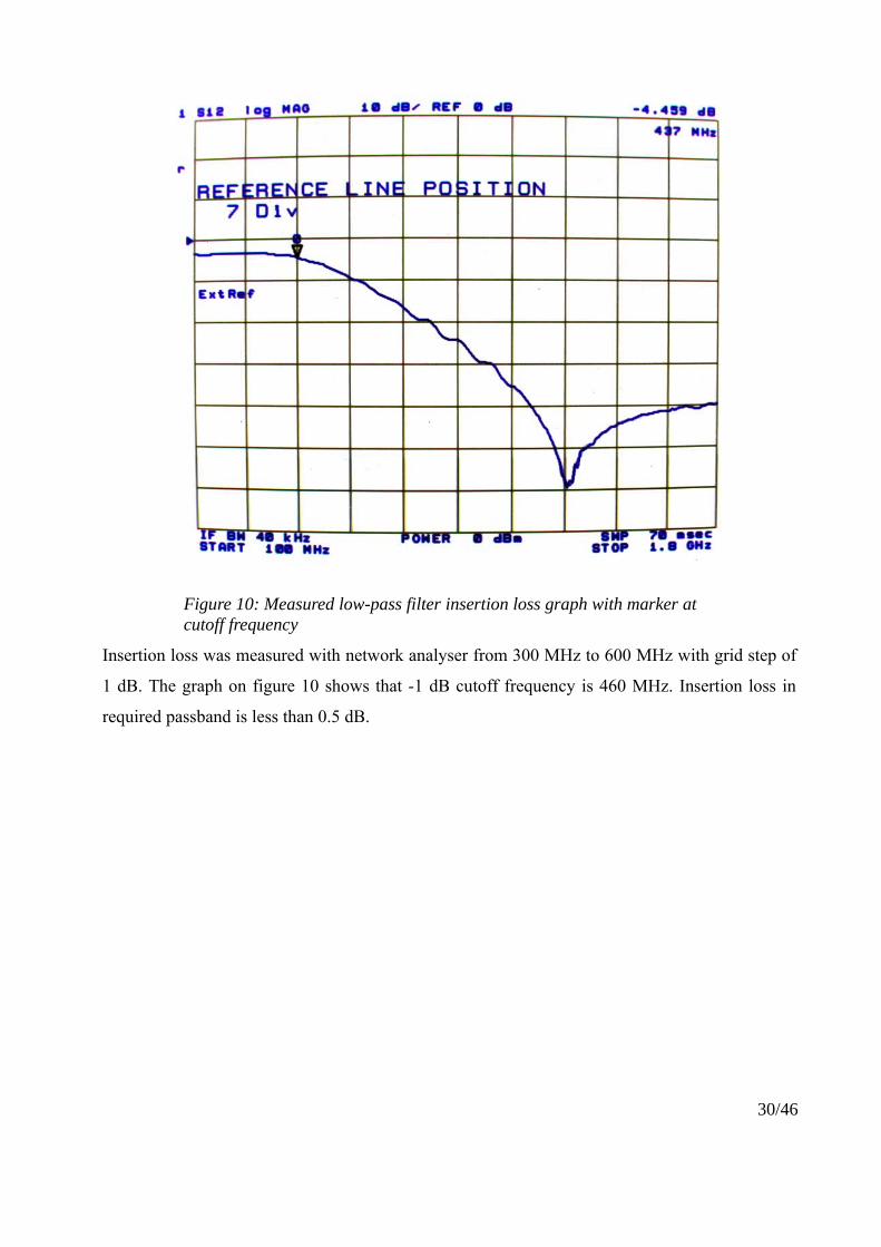
Measurements showed that with simulated 12 pF capacitors the cutoff frequency was too low,
only 407 MHz. Decreasing the capacitance increased filter cutoff frequency. Final capacitor value
was 8.2 pF that provided acceptable insertion losses and cutoff frequency.
29/46
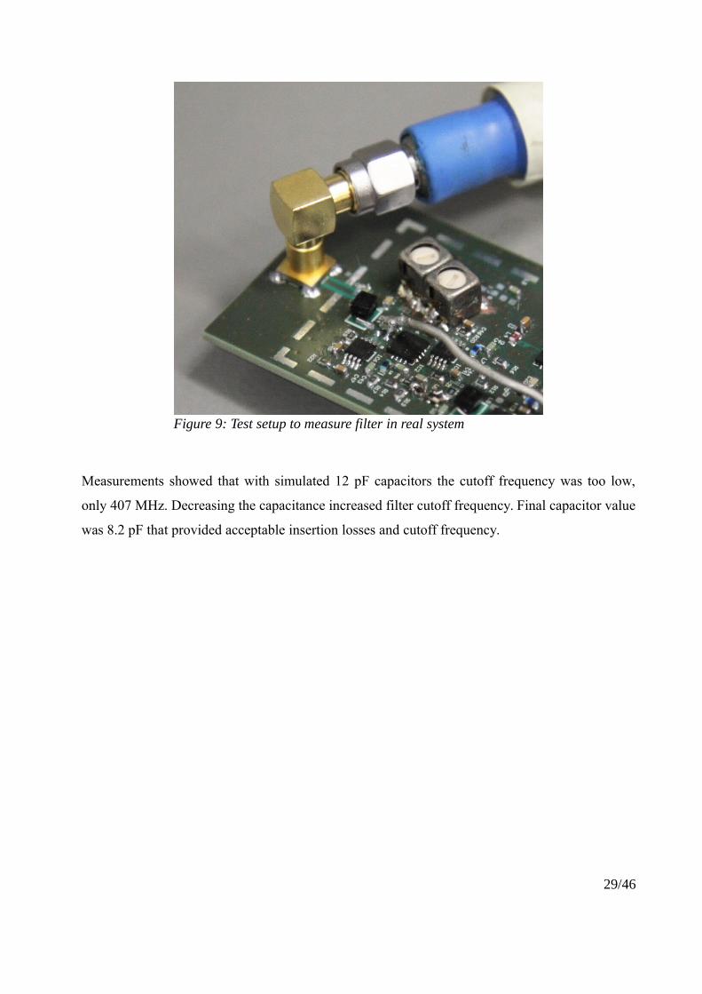
Figure 9: Test setup to measure filter in real system
Insertion loss was measured with network analyser from 300 MHz to 600 MHz with grid step of
1 dB. The graph on figure 10 shows that -1 dB cutoff frequency is 460 MHz. Insertion loss in
required passband is less than 0.5 dB.
30/46
Figure 10: Measured low-pass filter insertion loss graph with marker at cutoff frequency
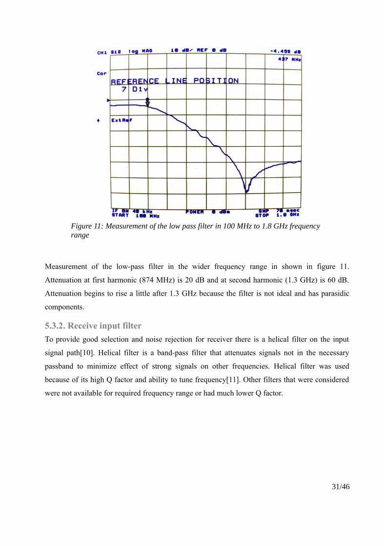
Measurement of the low-pass filter in the wider frequency range in shown in figure 11.
Attenuation at first harmonic (874 MHz) is 20 dB and at second harmonic (1.3 GHz) is 60 dB.
Attenuation begins to rise a little after 1.3 GHz because the filter is not ideal and has parasidic
components.
5.3.2. Receive input filter
To provide good selection and noise rejection for receiver there is a helical filter on the input
signal path[10]. Helical filter is a band-pass filter that attenuates signals not in the necessary
passband to minimize effect of strong signals on other frequencies. Helical filter was used
because of its high Q factor and ability to tune frequency[11]. Other filters that were considered
were not available for required frequency range or had much lower Q factor.
31/46
Figure 11: Measurement of the low pass filter in 100 MHz to 1.8 GHz frequency range
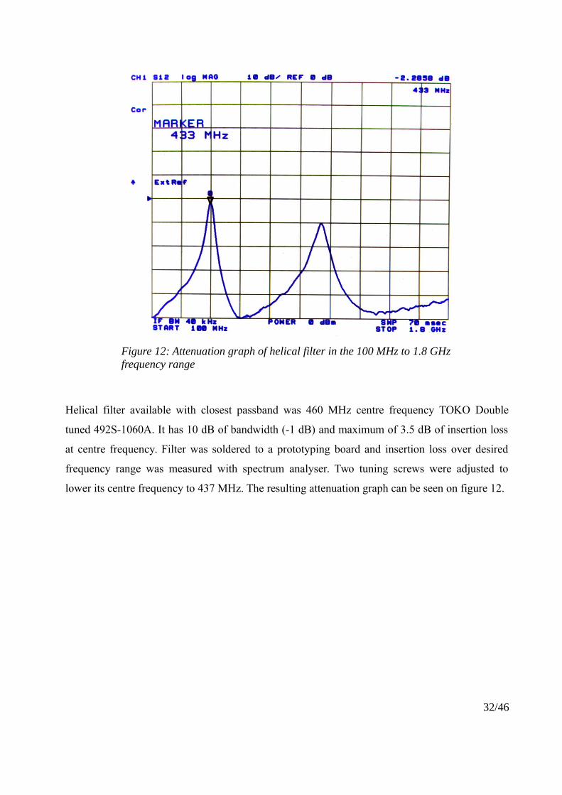
Helical filter available with closest passband was 460 MHz centre frequency TOKO Double
tuned 492S-1060A. It has 10 dB of bandwidth (-1 dB) and maximum of 3.5 dB of insertion loss
at centre frequency. Filter was soldered to a prototyping board and insertion loss over desired
frequency range was measured with spectrum analyser. Two tuning screws were adjusted to
lower its centre frequency to 437 MHz. The resulting attenuation graph can be seen on figure 12.
32/46
Figure 12: Attenuation graph of helical filter in the 100 MHz to 1.8 GHzfrequency range
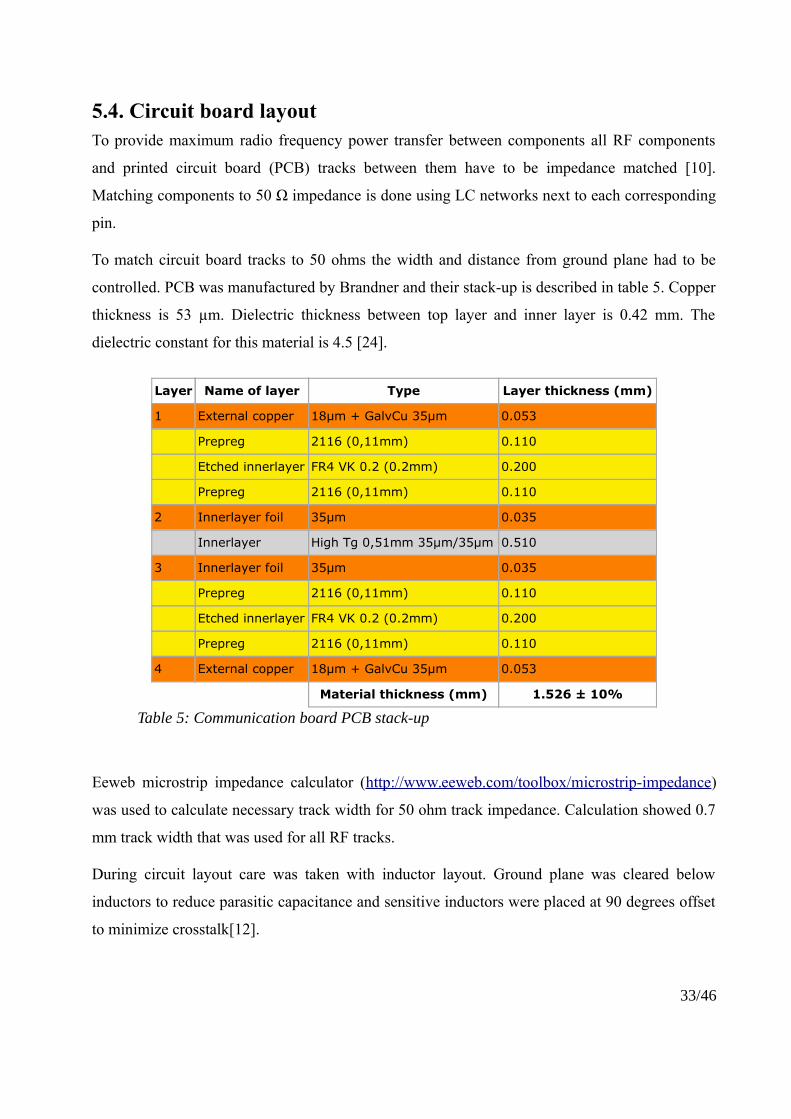
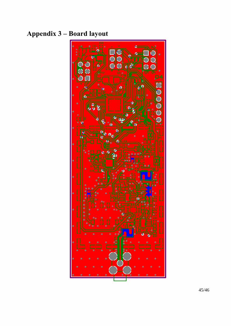
5.4. Circuit board layoutTo provide maximum radio frequency power transfer between components all RF components
and printed circuit board (PCB) tracks between them have to be impedance matched [10].
Matching components to 50 Ω impedance is done using LC networks next to each corresponding
pin.
To match circuit board tracks to 50 ohms the width and distance from ground plane had to be
controlled. PCB was manufactured by Brandner and their stack-up is described in table 5. Copper
thickness is 53 µm. Dielectric thickness between top layer and inner layer is 0.42 mm. The
dielectric constant for this material is 4.5 [24].
Eeweb microstrip impedance calculator (http://www.eeweb.com/toolbox/microstrip-impedance)
was used to calculate necessary track width for 50 ohm track impedance. Calculation showed 0.7
mm track width that was used for all RF tracks.
During circuit layout care was taken with inductor layout. Ground plane was cleared below
inductors to reduce parasitic capacitance and sensitive inductors were placed at 90 degrees offset
to minimize crosstalk[12].
33/46
Table 5: Communication board PCB stack-up
Layer Name of layer Type Layer thickness (mm)
1 External copper 18µm + GalvCu 35µm 0.053
Prepreg 2116 (0,11mm) 0.110
Etched innerlayer FR4 VK 0.2 (0.2mm) 0.200
Prepreg 2116 (0,11mm) 0.110
2 Innerlayer foil 35µm 0.035
Innerlayer High Tg 0,51mm 35µm/35µm 0.510
3 Innerlayer foil 35µm 0.035
Prepreg 2116 (0,11mm) 0.110
Etched innerlayer FR4 VK 0.2 (0.2mm) 0.200
Prepreg 2116 (0,11mm) 0.110
4 External copper 18µm + GalvCu 35µm 0.053
Material thickness (mm) 1.526 ± 10%

All of the RF circuitry is screened with surface mount tinned steel shield. The shield protects
receive circuitry from electromagnetic interference from other satellite subsystems and protects
other subsystems from high frequency emissions from transmitter.
Circuit and schematic were laid out by Ahti Laurisson under the supervision and guidance of
work author.
34/46
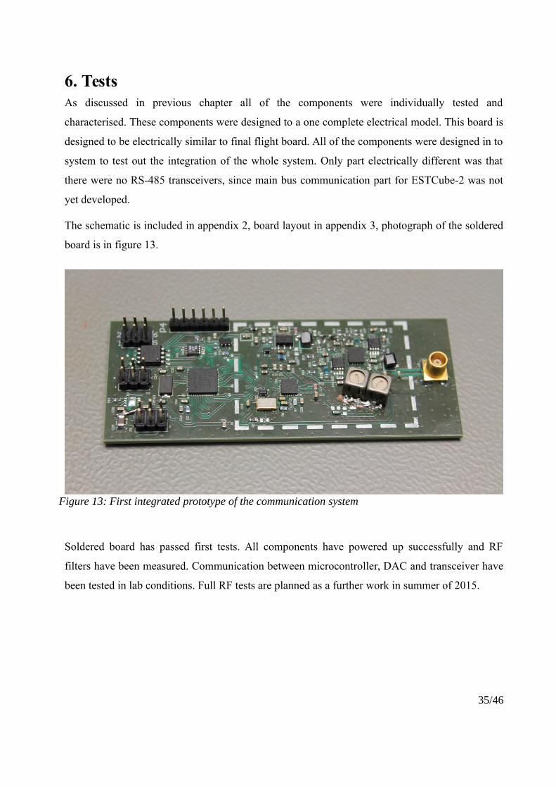
6. TestsAs discussed in previous chapter all of the components were individually tested and
characterised. These components were designed to a one complete electrical model. This board is
designed to be electrically similar to final flight board. All of the components were designed in to
system to test out the integration of the whole system. Only part electrically different was that
there were no RS-485 transceivers, since main bus communication part for ESTCube-2 was not
yet developed.
The schematic is included in appendix 2, board layout in appendix 3, photograph of the soldered
board is in figure 13.
Soldered board has passed first tests. All components have powered up successfully and RF
filters have been measured. Communication between microcontroller, DAC and transceiver have
been tested in lab conditions. Full RF tests are planned as a further work in summer of 2015.
35/46
Figure 13: First integrated prototype of the communication system
7. SummaryCommunication is one of the most important parts of any satellite. Estonian future satellite
ESTCube-2 needs a new and advanced communication system to upload commands and
firmware and download telemetry and images.
The goal of this masters thesis was to determine system architecture and develop first electrical
prototype of this communication system. Strengths and weaknesses of previous systems was
researched and new system design was determined. Necessary single components were
determined. Single components were built to prototypes, tested and characterised. RF parameters
of filters were measured and found to be suitable for the system. Components were integrated to
a first electrical model of the communication system. All of the work meets the requirements set
to the system. Since power is very limited on small satellites focus was making the
communication system energy efficient.
This work could not be done without support from people in ESTCube team. Most of the
necessary knowledge was taught by supervisors. Much of supporting work was done by other
members of communication subsystem team – Ahti Laurisson, Taavi Adamson and Laur Joost.
Work on the system continues in to develop full software and test all the component integration.
This work contains technical drawings and description of developed system. It also provides
information for developing other similar systems.
36/46
8. References1. “CubeSat Design Specification” (2014) The CubeSat Program
http://www.cubesat.org/images/developers/cds_rev13_final2.pdf Used 2015-05-14
2. “Announcement of CubeSat launch initiative” (2014) The National Aeronautics and
Space Administration
http://www.nasa.gov/sites/default/files/files/cubesat_launch_initiative_announcement_20
14_final(1).pdf Used 2015-05-14
3. Mike Safyan “Overview of the Planet Labs Constellation of Earth Imaging Satellites”
(2015) http://www.itu.int/en/ITU-R/space/workshops/2015-prague-small-
sat/Presentations/Planet-Labs-Safyan.pdf Used 2015-05-14
4. “ESTCube-1 nanosatellite for electric solar wind sail in-orbit technology demonstration”
(2014) Proceedings of the Estonian Academy of Sciences
5. “Analysis of the electrical power system for ESTCube-1” (2013) Proceedings of 64th
International Astronautical Congress
6. “Spectrum Requirements for the Amateur and Amateur-satellite Services” (2014)
International Amateur Radio Union
http://www.iaru.org/uploads/1/3/0/7/13073366/spectrum_requirements_rev2_nov_2014.p
df Used 2015-01-31
7. “ESTCube-1 radio details” http://www.estcube.eu/en/radio-details Used 2015-05-15
8. “MSP430FR59xx Mixed-Signal Microcontrollers ” (2014) Texas Instruments
http://www.ti.com/lit/ds/symlink/msp430fr5969.pdf Used 2015-01-20
9. Norman Dye , Helge Granberg (2001) “Radio Frequency Transistors”, pp 168
10. Joseph J. Carr (2002) “RF Components and Circuits”, pp 285, 52
11. C. J. Kikkert (2004-2009). “RF Electronics”, pp 191
12. “Application Note 1200.04 RF Design Guidelines: PCB Layout and Circuit
Optimization” (2006) Semtech
http://www.semtech.com/images/datasheet/rf_design_guidelines_semtech.pdf Used 2015-
37/46
01-23
13. “SGL0363Z 5MHz to 2000MHz low noise amplifier silicon germanium” (2006) RF
Micro Devices
http://www.rfmd.com/store/downloads/dl/file/id/28126/sgl0363z_data_sheet.pdf Used
2015-05-15
14. “NanoCom AX100 Datasheet” (2015) GomSpace ApS
http://www.gomspace.com/documents/gs-ds-nanocom-ax100-1.5.pdf Used 2015-05-15
15. “NanoCom U482C Datasheet v5.0 ” (2015) GomSpace ApS
http://www.gomspace.com/documents/GS-DS-U482C-5.0.pdf Used 2015-05-15
16. “UTRX Half Duplex UHF Transceiver” http://www.clyde-
space.com/cubesat_shop/communication_systems/350_utrx-half-duplex-uhf-transceiver
Used 2015-05-15
17. “TRXUV VHF/UHF Transceiver” Innovative Solutions In Space
http://www.isispace.nl/brochures/ISIS_TRXUV_Transceiver_Brochure_v.12.5.pdf Used
2015-05-15
18. Toomas Vahter "Tudengisatelliit ESTCube-1” (2010)
http://www.lr.ttu.ee/eriala/2010sygis/Eriala_1102.pdf Used 2015-05-15
19. Carlos Jorge Rodrigues Capela “Protocol of communications for VORSat satellite - link
budget” http://paginas.fe.up.pt/~ee97054/Link%20Budget.pdf Used 2015-05-16
20. “Link Budget Analysis: Digital Modulation, Part 2” (2013) Atlanta RF
www.atlantarf.com/FSK_Modulation.php Used 2015-05-16
21. “Si4464/63/61/60 high-performance, low-current transceiver” (2012) Silicon Laboratories
https://www.silabs.com/Support%20Documents/TechnicalDocs/Si4464-63-61-60.pdf
Used 2015-05-17
22. “TQP4M0010 High Isolation Absorptive SPDT Switch” (2013) TriQuint
http://www.triquint.com/products/d/DOC-B-00000236 Used 2015-05-17
23. "TQP7M9105 1W High Linearity Amplifier” (2014) TriQuint
http://www.triquint.com/products/d/doc-b-00000072 Used 2015-05-18
38/46
24. "High Reliability Glass Epoxy Multi-layer Materials (High Tg & Low CTE type)” (2011)
Panasonic
https://www3.panasonic.biz/em/pcbm/en/product/r1755v/2_data_sheet/10100721_HIPER
-V_R-1755V_R-1650V_2011_07_05.pdf Used 2015-05-18
39/46
9. KokkuvõteUHF-sagedusala sidesüsteem kuupsatelliidile
Side maaga on iga satelliidi üks kõige tähtsamatest osadest. Eesti tulevane satelliit ESTCube-2
vajab sidesüsteemi käskude ja info kahepidiseks vahetamiseks.
Selle magistritöö eesmärgiks oli panna paika süsteemi arhitektuur ja valmistada esimene
prototüüp. Töö alguses uuriti erinevaid olemasolevaid ja varem valmistatud lahendusi. Eelmise
sidesüsteemi ja uurimise järgi pandi paika uue süsteemi ülesehitus. Kõik üksikkomponendid
valiti välja. Tähtsamad komponentidest ehitati prototüübid, mida seejärel mõõdeti ja
iseloomustati. Filtrite komponendid testiti reaalse plaadi peal järgi ja mõõdeti kõik olulised
raadio parameetrid. Komponentidest pandi kokku esimene elektriliselt lõplik sidesüsteemi mudel,
millega tehti ka esimesed testid. Kõikide lõplike komponentide mõõtmised näitasid, et need
sobivad süsteemile seatud nõuetega kokku ja suudavad neid täita. Kuna miniatuursete satelliitide
peal on energia kogus piiratud oli fookus võimalikult energiaefektiivse süsteemi valmistamisel.
Töö süsteemiga jätkub. Ees ootab lõpliku tarkvara arendus ja terviksüsteemi põhjalik testimine
erinevates keskkondades.
Selles töös on arendatud süsteemi kogu dokumentatsioon – võrdlustabelid, tehnilised joonised ja
selgitused. Töö sisaldab ka informatsiooni teiste sarnaste süsteemide arendamiseks.
40/46
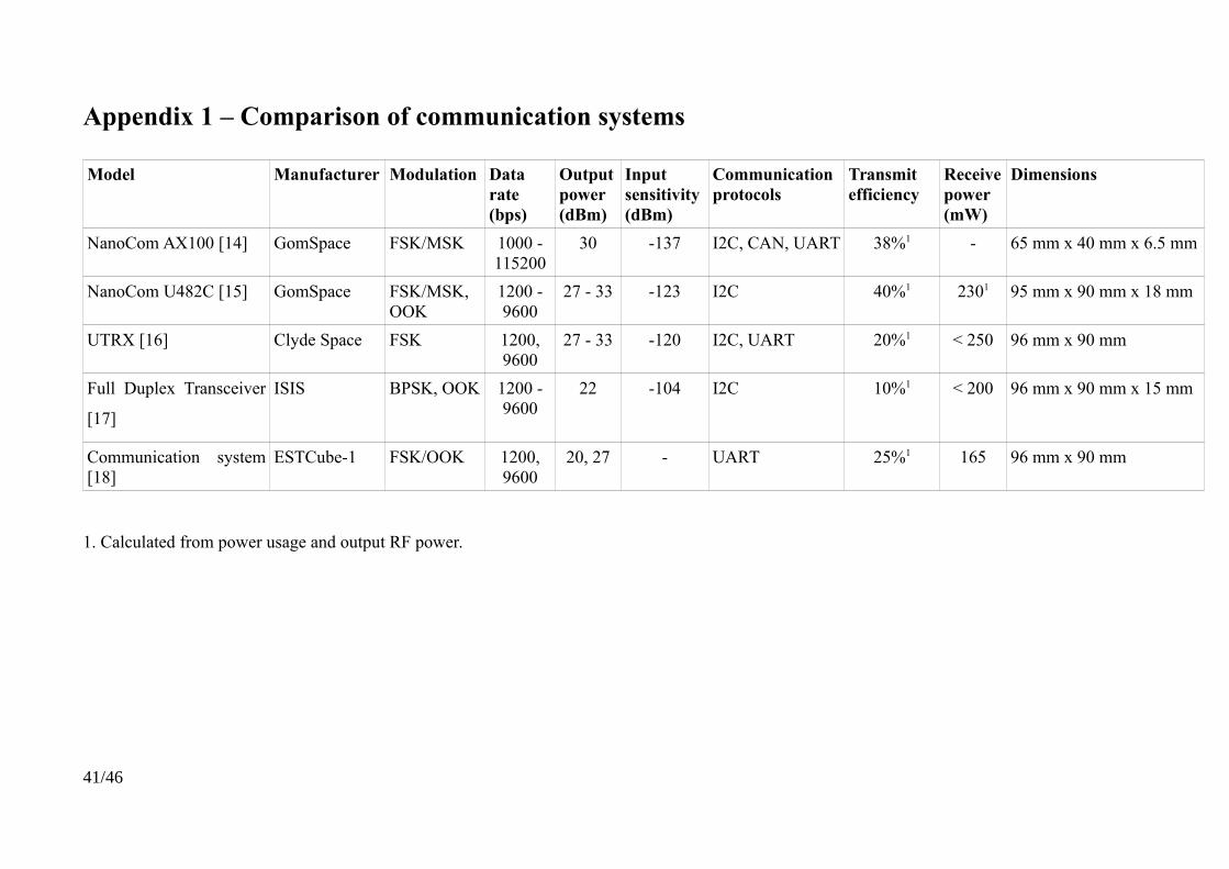
Appendix 1 – Comparison of communication systems
Model Manufacturer Modulation Datarate(bps)
Outputpower(dBm)
Inputsensitivity(dBm)
Communicationprotocols
Transmitefficiency
Receivepower(mW)
Dimensions
NanoCom AX100 [14] GomSpace FSK/MSK 1000 -115200
30 -137 I2C, CAN, UART 38%1 - 65 mm x 40 mm x 6.5 mm
NanoCom U482C [15] GomSpace FSK/MSK,OOK
1200 -9600
27 - 33 -123 I2C 40%1 2301 95 mm x 90 mm x 18 mm
UTRX [16] Clyde Space FSK 1200,9600
27 - 33 -120 I2C, UART 20%1 < 250 96 mm x 90 mm
Full Duplex Transceiver
[17]
ISIS BPSK, OOK 1200 -9600
22 -104 I2C 10%1 < 200 96 mm x 90 mm x 15 mm
Communication system[18]
ESTCube-1 FSK/OOK 1200,9600
20, 27 - UART 25%1 165 96 mm x 90 mm
1. Calculated from power usage and output RF power.
41/46
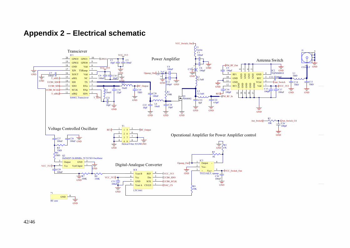
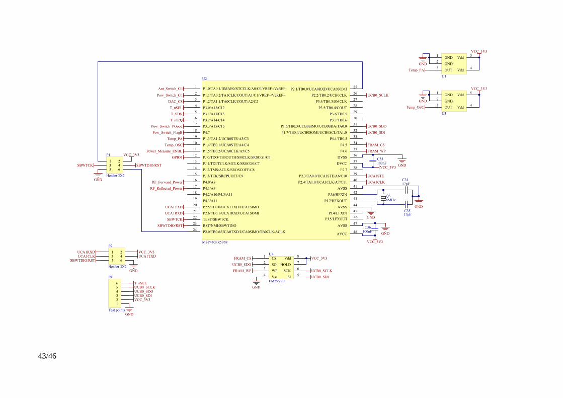
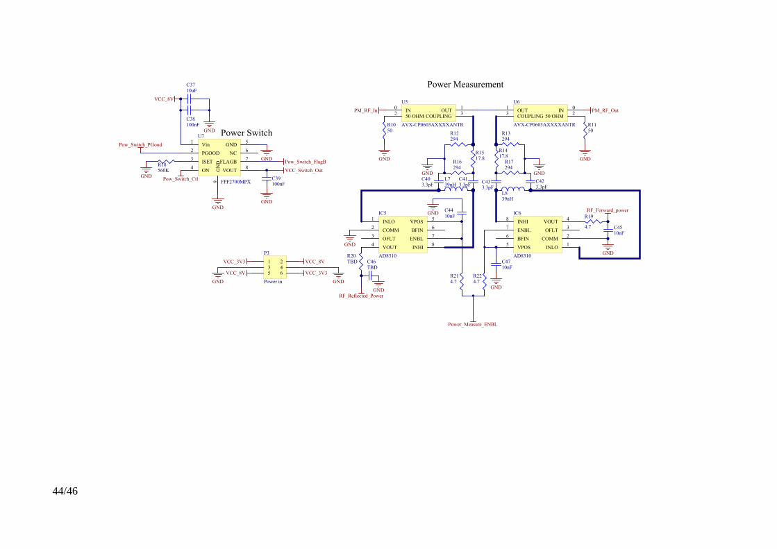
Appendix 2 – Electrical schematic
42/46
SDN 1RXp
2RXn
3TX
4NC
5Vdd
6TXRamp
7Vdd
8GPIO0
9GPIO1
10
nIRQ11SCLK
12SDO
13SDI
14nSEL
15XOUT
16XIN
17GND
18GPIO2
19GPIO3
20IC1
Si4463, Transciever
T_nSEL
UCB0_SDO
UCB0_SDI
UCB0_SCLK
T_nIRQ
GND
VCC_3V3
RF_Output
22pFC18
220nHL4
10pF
C21
GND
Voltage Controlled Oscillator
Transciever
Digital-Analogue Converter Output1
Vcc-2
+3
-4
Vcc+5
IC3
TS321AILT, opamp
10KR9
GNDVCC_Switch_Out
1K
R5
1KR3
GND
Opamp_Out
Operational Amplifier for Power Amplifier control
Power Amplifier Antenna Switch
56nH
L3
100nFC7
GND
Q1PD84002
Vdd1
VCtrl2
RFC3
GND4
GN
D5
GN
D6
GN
D7
GN
D8
RF19
GND10
GND11
RF212
GN
D13
GN
D14
GN
D15
GN
D16
GN
D17
IC2TQP4M0010
10pFC24
10nHL6
18pFC25
GND
100nFC20
VCC_3V3
Ant_Switch
RF_Output
GND
GND
GND
12.5nHL5
6.8pFC22
150RR1
100nFC4
GND
12.5nHL2
100nFC1
GND
VCC_Switch_Out
100pFC5
100pFC16
100nFC17
FerriteF1
1
2
3C8
Opamp_Out
CS/LD 1SCK
2Din
3REF
4Vout B
5
Vcc6
GND7
Vout A8
IC4
LTC1661
UCB0_SDO
UCB0_SCLK
DAC_CS
GND
VCC_3V3
VCC_3V3
GNDVCC_3V3
100KR7
330KR8
GND
Vctrl Input1
GND2
Output3
Vcc4
Q2OeD4207-26.00MHz, TCVCXO Oscillator
TBDR6
TBDR4
100nFC27
100nFC28
GND
100nFC3
GND100nFC9
VCC_3V3
100nFC29
100nFC31
GND
100nFC30
GND
10pFC2
10pFC10
GND GND
100pFC12
100pFC6
100pFC15
T_SDN
Ant_Switch10K
R2
100pFC26
GND
Ant_Switch_Ctl
TBDC14
GND
100pFC11 TBDL1
TBDC13
GND
GND
GND
0pFC23
GND
TBDC19
GND
5
1
234
J1
COAX-F GND
PM_RF_In
PM_RF_Out
11
22
33
44
55
66
77
88
T1
Helical Filter 5CGWGND
GND
RF2
RF2
GND
GND0
*1
RF case
1
2
3
C32
GND
GPIO1
43/46
Q38MHz
17pFC34
17pFC35
GND
GND
UCB0_SCLK
UCB0_SDO
UCB0_SDI
UCA1CLK
DAC_CS
VCC_3V3
GND
VCC_3V3GND
Ant_Switch_Ctl
Pow_Switch_Ctl
100nFC33
100nFC36
T_nSEL
T_SDN
T_nIRQ
Pow_Switch_PGood
Pow_Switch_FlagB
GND
VCC_3V3
1 23 45 6
P1
Header 3X2
GND1
GND2
OUT3
Vdd4
Vdd5
U1
GND1
GND2
OUT3
Vdd4
Vdd5
U3
VCC_3V3
VCC_3V3
GND
GND
Temp_PA
Temp_OSC
Temp_PA
Temp_OSC
RF_Reflected_Power
RF_Forward_Power
Power_Measure_ENBL
P1.0/TA0.1/DMAE0/RTCCLK/A0/C0/VREF-/VeREF-1
P1.1/TA0.2/TA1CLK/COUT/A1/C1/VREF+/VeREF+2
P1.2/TA1.1/TA0CLK/COUT/A2/C23
P3.0/A12/C124
P3.1/A13/C135
P3.2/A14/C146
P3.3/A15/C157
P4.78
P1.3/TA1.2/UCB0STE/A3/C39
P1.4/TB0.1/UCA0STE/A4/C410
P1.5/TB0.2/UCA0CLK/A5/C511
PJ.0/TDO/TB0OUTH/SMCLK/SRSCG1/C612
PJ.1/TDI/TCLK/MCLK/SRSCG0/C713
PJ.2/TMS/ACLK/SROSCOFF/C814
PJ.3/TCK/SRCPUOFF/C915
P4.0/A816
P4.1/A917
P4.2/A10/P4.3/A1118
P4.3/A1119
P2.5/TB0.0/UCA1TXD/UCA1SIMO20
P2.6/TB0.1/UCA1RXD/UCA1SOMI21
TEST/SBWTCK22
RST/NMI/SBWTDIO23
P2.0/TB0.6/UCA0TXD/UCA0SIMO/TB0CLK/ACLK24
P2.1/TB0.0/UCA0RXD/UCA0SOMI25
P2.2/TB0.2/UCB0CLK 26
P3.4/TB0.3/SMCLK27
P3.5/TB0.4/COUT28
P3.6/TB0.529
P3.7/TB0.630
P1.6/TB0.3/UCB0SIMO/UCB0SDA/TA0.031
P1.7/TB0.4/UCB0SOMI/UCB0SCL/TA1.032
P4.4/TB0.5 33
P4.534
P4.6 35
DVSS36
DVCC37
P2.738
P2.3/TA0.0/UCA1STE/A6/C1039
P2.4/TA1.0/UCA1CLK/A7/C1140
AVSS41
PJ.6/HFXIN 42
PJ.7/HFXOUT43
AVSS44
PJ.4/LFXIN45
PJ.5/LFXOUT46
AVSS47
AVCC48
U2
MSP430FR5969
1 23 45 6
P2
Header 3X2
UCA1TXD
UCA1RXD
UCA1STE
VCC_3V3UCA1RXD
GND
SBWTCK
SBWTCK
SBWTDIO/RST
UCA1CLK UCA1TXD
SBWTDIO/RST
SBWTDIO/RSTCS1
SO2
WP3
Vss4
SI5
SCK6
HOLD7
Vdd 8U4
FM25V20
UCB0_SDO
UCB0_SDI
UCB0_SCLK
VCC_3V3
GND
FRAM_CS
FRAM_CS
FRAM_WP
FRAM_WP
GPIO1
123456
P4
Test points
UCB0_SDOUCB0_SDI
UCB0_SCLK
VCC_3V3
GND
T_nSEL
44/46
Vin1
PGOOD2
ISET3
ON4
GND5
NC 6
FLAGB7
VOUT8G
ND
9
U7
FPF2700MPX
VCC_8V
100nFC38
GND
Pow_Switch_PGood
560KR18
GNDPow_Switch_Ctl
GNDPow_Switch_FlagB
VCC_Switch_Out
100nFC39
GND
Power Switch
GND
10uFC37
GND
VCC_8V
VCC_3V3
GND
VCC_3V3
VCC_8V1 23 45 6
P3
Power in
INLO1
COMM2
OFLT3
VOUT4
VPOS 5
BFIN6
ENBL 7
INHI8
IC5
AD8310
Power Measurement
INLO1
COMM 2OFLT
3VOUT 4
VPOS5
BFIN6ENBL
7INHI8
IC6
AD8310
50R10
50R11
294R16
IN0
OUT1
50 OHM2
COUPLING3
U5
AVX-CP0603AXXXXANTR
IN0
OUT1
50 OHM2
COUPLING3
U6
AVX-CP0603AXXXXANTR
GND GND17.8R15
294R12
GND
294R13
17.8R14
294R17
GND
3.3pFC41
39nHL7
3.3pFC40
GND
3.3pFC42
39nHL8
3.3pFC43
GND
4.7R21
4.7R22
Power_Measure_ENBL
TBDR20
TBDC46
GNDRF_Reflected_Power
10nFC44
GND
10nFC47
GND
4.7
R19
10nFC45
RF_Forward_power
PM_RF_In PM_RF_Out
Appendix 3 – Board layout
45/46
Non-exclusive licence to reproduce thesis and make thesis public
I, Jaanus Kalde
1. herewith grant the University of Tartu a free permit (non-exclusive licence) to:
1.1. reproduce, for the purpose of preservation and making available to the public, including foraddition to the DSpace digital archives until expiry of the term of validity of the copyright,and
1.2. make available to the public via the web environment of the University of Tartu, includingvia the DSpace digital archives until expiry of the term of validity of the copyright,
UHF COMMUNICATION SYSTEM FOR CUBESATELLITE,
supervised by Viljo Allik,
2. I am aware of the fact that the author retains these rights.
3. I certify that granting the non-exclusive licence does not infringe the intellectual propertyrights or rights arising from the Personal Data Protection Act.
Tartu, 15.05.2015
46/46


![Sulev Jaanus haldusjuht - ekkliit.ee...(Microsoft PowerPoint - Sulev Jaanus esitlus 22.02.2019 [ hilduvusre iim]) Author EKHHL Created Date 2/19/2019 12:47:44 PM](https://img.pdfslide.net/doc/110x75/5f0af6717e708231d42e327e/sulev-jaanus-haldusjuht-microsoft-powerpoint-sulev-jaanus-esitlus-22022019.jpg)