Embed Size (px)
Citation preview

Rev.1.2.0 2015-09-16
UHF RFID Reader/Writer Module
Specification
2 of 22
RED4 Specification
Contents
Revision History ............................................................................................................................................... 3 1 Overview ............................................................................................................................................ 4 2 Electrical Specification ..................................................................................................................... 5 2.1 Absolute Maximum Ratings ................................................................................................................ 5 2.2 Functional specification ....................................................................................................................... 5 3 Pin Description .................................................................................................................................. 6 4 Application Circuit ............................................................................................................................ 8 4.1 Power Supply ...................................................................................................................................... 8 4.2 RESETb .............................................................................................................................................. 8 4.3 UART ................................................................................................................................................... 9 4.4 I2C Interface ........................................................................................................................................ 9 4.5 SSP Interface .................................................................................................................................... 10 4.6 GPIO.................................................................................................................................................. 10 4.7 External Interrupt ............................................................................................................................... 10 4.8 ISP Mode ........................................................................................................................................... 10 4.9 Debugger ........................................................................................................................................... 10 4.10 Operation Mode Control .................................................................................................................... 11 4.11 Available GPIO .................................................................................................................................. 12 5 Channel Number Table ................................................................................................................... 13 5.1 US band ............................................................................................................................................ 13 5.2 North America band .......................................................................................................................... 14 5.3 Korea band ........................................................................................................................................ 15 5.4 China band ........................................................................................................................................ 15 5.5 Japan band ........................................................................................................................................ 16 5.6 EU band ............................................................................................................................................ 16 5.7 Brazil band ........................................................................................................................................ 17 6 Dimension ........................................................................................................................................ 18 7 Footprint ........................................................................................................................................... 19 8 Packing Information ........................................................................................................................ 20 8.1 Inner foam sheet dimension .............................................................................................................. 20 8.2 Outer box dimension ......................................................................................................................... 20 9 Reflow information .......................................................................................................................... 21 10 Address Information ....................................................................................................................... 22

3 of 22
RED4 Specification
Revision History
Version Date Page Description
1.0.0 2014.10.20 Preliminary
1.0.1 2015.01.12 Preliminary , fixed typo error, modified block diagram
1.0.2 2015.04.13 Preliminary, fixed spec
1.1.0 2015.05.14 Add reset IC, fixed spec, add available GPIO
1.1.1 2015.06.02 Change name, fixed spec, remove deepsleep mode
1.1.2 2015.06.30 Change current spec
1.1.3 2015.07.28
Add reflow chart
Modify channel table
Add information to 2.Electrical specification
1.2.0 2015.09.16
Modify channel table (for Brazil)
Modify Hardware : RED4A1
- modify CSE related function
- change Shield can
- change filter component
4 of 22
RED4 Specification
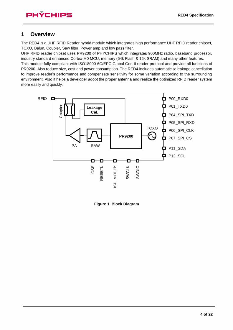
1 Overview
The RED4 is a UHF RFID Reader hybrid module which integrates high performance UHF RFID reader chipset,
TCXO, Balun, Coupler, Saw filter, Power amp and low pass filter.
UHF RFID reader chipset uses PR9200 of PHYCHIPS which integrates 900MHz radio, baseband processor,
industry standard enhanced Cortex-M0 MCU, memory (64k Flash & 16k SRAM) and many other features.
This module fully compliant with ISO18000-6C/EPC Global Gen II reader protocol and provide all functions of
PR9200. Also reduce size, cost and power consumption. The RED4 includes automatic tx leakage cancellation
to improve reader’s performance and compensate sensitivity for some variation according to the surrounding
environment. Also it helps a developer adopt the proper antenna and realize the optimized RFID reader system
more easily and quickly.
PR9200
SAW
TCXO
PA
RFIO
Leakage
Cal.
Coup
ler
P00_RXD0
P01_TXD0
P04_SPI_TXD
P05_SPI_RXD
P06_SPI_CLK
P07_SPI_CS
CS
E
P11_SDA
P12_SCL
RE
SE
Tb
SW
LC
K
SW
DIO
ISP
_M
OD
Eb
Figure 1 Block Diagram
SW
CLK
5 of 22
RED4 Specification
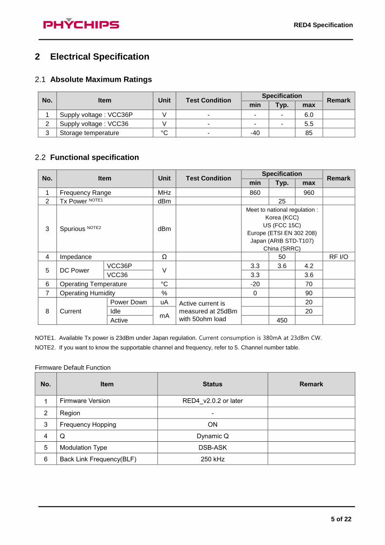
2 Electrical Specification
2.1 Absolute Maximum Ratings
No. Item Unit Test Condition Specification
Remark min Typ. max
1 Supply voltage : VCC36P V - - - 6.0
2 Supply voltage : VCC36 V - - - 5.5
3 Storage temperature °C - -40 85
2.2 Functional specification
No. Item Unit Test Condition Specification
Remark min Typ. max
1 Frequency Range MHz 860 960
2 Tx Power NOTE1 dBm 25
3 Spurious NOTE2 dBm
Meet to national regulation :
Korea (KCC)
US (FCC 15C)
Europe (ETSI EN 302 208)
Japan (ARIB STD-T107)
China (SRRC)
4 Impedance Ω 50 RF I/O
5 DC Power VCC36P
V 3.3 3.6 4.2
VCC36 3.3 3.6
6 Operating Temperature °C -20 70
7 Operating Humidity % 0 90
8 Current
Power Down uA Active current is
measured at 25dBm
with 50ohm load
20
Idle mA
20
Active 450
NOTE1. Available Tx power is 23dBm under Japan regulation. Current consumption is 380mA at 23dBm CW.
NOTE2. If you want to know the supportable channel and frequency, refer to 5. Channel number table.
Firmware Default Function
No. Item Status Remark
1 Firmware Version RED4_v2.0.2 or later
2 Region -
3 Frequency Hopping ON
4 Q Dynamic Q
5 Modulation Type DSB-ASK
6 Back Link Frequency(BLF) 250 kHz
6 of 22
RED4 Specification
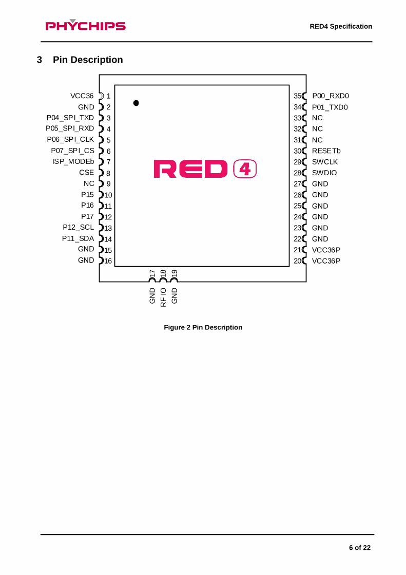
3 Pin Description
1
2
3
4
5
6
7
8
9
10
11
12
13
14
15
16
17
18
19
20
21
22
23
24
25
26
27
28
29
30
31
32
33
34
35VCC36
GND
NC
P01_TXD0
P04_SPI_TXD
P05_SPI_RXD
P06_SPI_CLK
P07_SPI_CS
ISP_MODEb
CSE
NC
P15
P16
P17
P12_SCL
P11_SDA
P00_RXD0
NC
NC
RESETb
SWCLK
SWDIO
GND
GND
GND
GND
GND
GND
VCC36P
VCC36P
PRM92A40AE
GN
D
RF
IO
GN
D
Figure 2 Pin Description
7 of 22
RED4 Specification
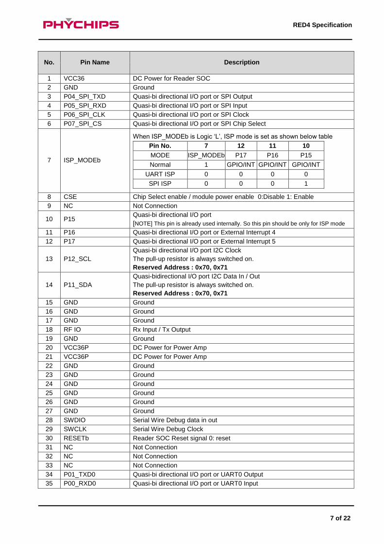
No. Pin Name Description
1 VCC36 DC Power for Reader SOC
2 GND Ground
3 P04_SPI_TXD Quasi-bi directional I/O port or SPI Output
4 P05_SPI_RXD Quasi-bi directional I/O port or SPI Input
5 P06_SPI_CLK Quasi-bi directional I/O port or SPI Clock
6 P07_SPI_CS Quasi-bi directional I/O port or SPI Chip Select
7 ISP_MODEb
When ISP_MODEb is Logic ‘L’, ISP mode is set as shown below table
Pin No. 7 12 11 10
MODE ISP_MODEb P17 P16 P15
Normal 1 GPIO/INT GPIO/INT GPIO/INT
UART ISP 0 0 0 0
SPI ISP 0 0 0 1
8 CSE Chip Select enable / module power enable 0:Disable 1: Enable
9 NC Not Connection
10 P15 Quasi-bi directional I/O port
[NOTE] This pin is already used internally. So this pin should be only for ISP mode
11 P16 Quasi-bi directional I/O port or External Interrupt 4
12 P17 Quasi-bi directional I/O port or External Interrupt 5
13 P12_SCL
Quasi-bi directional I/O port I2C Clock
The pull-up resistor is always switched on.
Reserved Address : 0x70, 0x71
14 P11_SDA
Quasi-bidirectional I/O port I2C Data In / Out
The pull-up resistor is always switched on.
Reserved Address : 0x70, 0x71
15 GND Ground
16 GND Ground
17 GND Ground
18 RF IO Rx Input / Tx Output
19 GND Ground
20 VCC36P DC Power for Power Amp
21 VCC36P DC Power for Power Amp
22 GND Ground
23 GND Ground
24 GND Ground
25 GND Ground
26 GND Ground
27 GND Ground
28 SWDIO Serial Wire Debug data in out
29 SWCLK Serial Wire Debug Clock
30 RESETb Reader SOC Reset signal 0: reset
31 NC Not Connection
32 NC Not Connection
33 NC Not Connection
34 P01_TXD0 Quasi-bi directional I/O port or UART0 Output
35 P00_RXD0 Quasi-bi directional I/O port or UART0 Input

8 of 22
RED4 Specification
4 Application Circuit
Figure 3 Application Circuit
Figure 3 show example of application circuit of RED4. According to your application, you can use a variety of
structure.
4.1 Power Supply DC power to operate RED4 is separated by 2 kinds. VCC36 is to supply for PR9200 which power range is 3.3
to 3.6 volts, VCC36P is to supply for power amp which power range is 3.3 to 4.2 volts. Total current consumption
of RED4 is typically 450mA at 25dBm output power.
In mobile device with battery, VCC36P can be connected to battery power directly. VCC36 pins need to external
LDO (or other device). As the Host control the LDO’s enable, user control power down mode of module.
If you do not control external LDO, you can control CSE pin to enter power down mode instead.
4.2 RESETb RED4 provides RESET for controlling PR9200, which can control by RESETb (Pin 30).
In order to properly operate RESET function, RESETb pin should be connected to ground during at least 2us.
[NOTE] RED4 have internal RESET circuit including POR (Power On Reset) and BOD (Brown Output
Detector). When you power up, reset time is made internally by RESET circuit. Although you enter POWER
DOWN mode by asserted CSE to logic low, the RESET circuit is also operated when exit POWER DOWN by
asserted CSE to logic high.
9 of 22
RED4 Specification
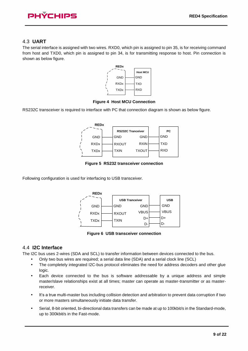
4.3 UART The serial interface is assigned with two wires. RXD0, which pin is assigned to pin 35, is for receiving command
from host and TXD0, which pin is assigned to pin 34, is for transmitting response to host. Pin connection is
shown as below figure.
Host MCU
TXDx
RXDx
GND
TXD
RXD
GND
REDx
Figure 4 Host MCU Connection
RS232C transceiver is required to interface with PC that connection diagram is shown as below figure.
RS232C Tranceiver
TXDx
RXDx
GND
RXOUT
TXIN
GND
TXOUT
RXIN
GND
PC
TXD
RXD
GND
REDx
Figure 5 RS232 transceiver connection
Following configuration is used for interfacing to USB transceiver.
USB Tranceiver
TXDx
RXDx
GND
RXOUT
TXIN
GND
D+
VBUS
GND
USB
D-
D+
VBUS
GND
D-
REDx
Figure 6 USB transceiver connection
4.4 I2C Interface The I2C bus uses 2-wires (SDA and SCL) to transfer information between devices connected to the bus.
Only two bus wires are required; a serial data line (SDA) and a serial clock line (SCL)
The completely integrated I2C-bus protocol eliminates the need for address decoders and other glue
logic.
Each device connected to the bus is software addressable by a unique address and simple
master/slave relationships exist at all times; master can operate as master-transmitter or as master-
receiver.
It’s a true multi-master bus including collision detection and arbitration to prevent data corruption if two
or more masters simultaneously initiate data transfer.
Serial, 8-bit oriented, bi-directional data transfers can be made at up to 100kbit/s in the Standard-mode,
up to 300kbit/s in the Fast-mode.

10 of 22
RED4 Specification
The number of Ics that can be connected to the same bus is limited only by a maximum bus
capacitance of 400pF.
4.5 SSP Interface The SSP is a master or slave interface for SPI synchronous serial communication with peripheral devices.
Programmable clock bit rate and prescale.
Separate transmit and receive first-in, first-out memory buffers, 16 bits wide, 8 locations deep.
Programmable choice of LSB first or MSB first data frame and data frame size from 4 to 16 bits.
Independent masking of transmit FIFO, receive FIFO, and receive overrun interrupt.
Internal loopback test mode available.
4.6 GPIO RED4 provides 9 bi-directional I/O ports.
4.7 External Interrupt RED4 provides 2 external interrupt that is unstoppable except by reset.
Dedicated non-maskable Interrupt input.
Support for both level-sensitive and pulse-sensitive interrupt lines.
4.8 ISP Mode
In order to enter UART ISP mode, some hardware setting is required.
Set pins ISP_MODEb, P17, P16 and P15 to logic “0”.
Mode name H/W control
Programming Port ISP_MODEb P17 P16 P15
ISP UART 0 0 0 0 UART0
[NOTE1] Firmware download can be executed by IAP mode without hardware control under normal condition.
[NOTE2] P15 is already used internally. If you fix P15 to zero for SIP mode in your board, RED4 could have
some problem. So this pin should be only for ISP mode
4.9 Debugger
In order to debug firmware, these ports should be connected with H/W debugger which is available on both the
ULINK2 and Co-LINK. (For details, please refer to the ‘RED_FDM.pdf’)

11 of 22
RED4 Specification
4.10 Operation Mode Control RED4 is configured in 5 main modes of operation according to PR9200.
The following table describes block condition and current according to each operation state.
Operation state
State name HW set PR9200 PAM
current Function Analog Digital PA
POWER
DOWN
CSE=0 OFF OFF OFF 20uA Module power off
SLEEP CSE=1 OFF Sleep OFF 14mA Sleep mode,
Wake-up
internal/external
interrupt.
IDLE CSE=1 OFF ON OFF 20mA Block initialization
ACTIVE CSE=1 ON ON ON 450 mA1) Ramp-up
Tag read / write /
access / lock ..
Ramp-down
[Note] 1) Active current is measured at Tx CW condition.
The state diagram shows the modes RED4 can operate in. it also include transition time between the states.
When RED4 enter ACTIVE mode, RF Block is activated and ramp-up the system and it start to read RFID tag.
Entering IDLE mode from POWER DOWN mode, initial time is needed. MCU initial time is 3.9ms including
system power ON. MODEM & RF initial time take about 6ms.
POWER DOWN
IDLE
SLEEP
CSE=0
H/W control
F/W control
CSE=0
CSE=1
MCU initial time 3.9ms
RF/MODEM initial time
6ms
state
Transi-tion
Internal or External interrupt
Sleep mode
TRANSMISSION START
CSE=0
TRANSMISSION STOP
RESETb=0->1
ACTIVE
RESETb=0->1
REPEAT
Wakeup time
10.3us
Figure 7 Operation Sequence

12 of 22
RED4 Specification
4.11 Available GPIO
RED4 is based on PR9200 SOC. In order to configure the functions of module, some GPIO of PR9200 are
already used. Below table shows the available GPIO.
GPIO GPIO Function RED4
P00 UART0 RXD UART_RXD0
P01 UART0 TXD UART_TXD0
P02 Ext.0 Internally used (Ext PA_EN)
P03 Ext.1 Internally used
P04 SSP TXDS
P05 SSP RXDS
P06 SSP SCK
P07 SSP SEL
P10 Ext.2 Internally used
P11 I2C SDA Internally used NOTE1
P12 I2C SCL Internally used NOTE1
P13 UART1 RXD(Ext.3) Internally used
P14 UART1 TXD Internally used
P15 - Internally used
P16 Ext.4 IRQ (SPI, I2C)NOTE2
P17 Ext.5
NOTE1. Current Slave address 0x70, 0x71 are used. Other Slave address are available
NOTE2. When you use SPI or I2C Interface, P16 is required. If not, you can use this pin

13 of 22
RED4 Specification
5 Channel Number Table
5.1 US band
Channel Channel Frequency Channel Channel Frequency
1 917.10 MHz 26 922.10 MHz
2 917.30 MHz 27 922.30 MHz
3 917.50 MHz 28 922.50 MHz
4 917.70 MHz 29 922.70 MHz
5 917.90 MHz 30 922.90 MHz
6 918.10 MHz 31 923.10 MHz
7 918.30 MHz 32 923.30 MHz
8 918.50 MHz 33 923.50 MHz
9 918.70 MHz 34 923.70 MHz
10 918.90 MHz 35 923.90 MHz
11 919.10 MHz 36 924.10 MHz
12 919.30 MHz 37 924.30 MHz
13 919.50 MHz 38 924.50 MHz
14 919.70 MHz 39 924.70 MHz
15 919.90 MHz 40 924.90 MHz
16 920.10 MHz 41 925.10 MHz
17 920.30 MHz 42 925.30 MHz
18 920.50 MHz 43 925.50 MHz
19 920.70 MHz 44 925.70 MHz
20 920.90 MHz 45 925.90 MHz
21 921.10 MHz 46 926.10 MHz
22 921.30 MHz 47 926.30 MHz
23 921.50 MHz 48 926.50 MHz
24 921.70 MHz 49 926.70 MHz
25 921.90 MHz 50 926.90 MHz
[NOTE] The available band in US is from 902MHz to 928MHz. but in many application, antennas can’t cover
this all range. So RED series support narrow US band. It also meet FCC regulation.
If you want, you can use all US band named North America band as table 5.2
14 of 22
RED4 Specification
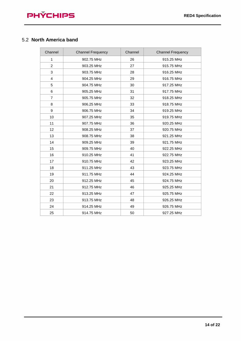
5.2 North America band
Channel Channel Frequency Channel Channel Frequency
1 902.75 MHz 26 915.25 MHz
2 903.25 MHz 27 915.75 MHz
3 903.75 MHz 28 916.25 MHz
4 904.25 MHz 29 916.75 MHz
5 904.75 MHz 30 917.25 MHz
6 905.25 MHz 31 917.75 MHz
7 905.75 MHz 32 918.25 MHz
8 906.25 MHz 33 918.75 MHz
9 906.75 MHz 34 919.25 MHz
10 907.25 MHz 35 919.75 MHz
11 907.75 MHz 36 920.25 MHz
12 908.25 MHz 37 920.75 MHz
13 908.75 MHz 38 921.25 MHz
14 909.25 MHz 39 921.75 MHz
15 909.75 MHz 40 922.25 MHz
16 910.25 MHz 41 922.75 MHz
17 910.75 MHz 42 923.25 MHz
18 911.25 MHz 43 923.75 MHz
19 911.75 MHz 44 924.25 MHz
20 912.25 MHz 45 924.75 MHz
21 912.75 MHz 46 925.25 MHz
22 913.25 MHz 47 925.75 MHz
23 913.75 MHz 48 926.25 MHz
24 914.25 MHz 49 926.75 MHz
25 914.75 MHz 50 927.25 MHz
15 of 22
RED4 Specification
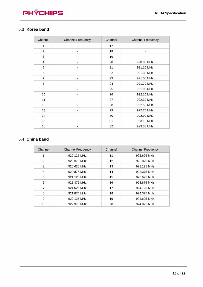
5.3 Korea band
Channel Channel Frequency Channel Channel Frequency
1 - 17 -
2 - 18 -
3 - 19 -
4 - 20 920.90 MHz
5 - 21 921.10 MHz
6 - 22 921.30 MHz
7 - 23 921.50 MHz
8 - 24 921.70 MHz
9 - 25 921.90 MHz
10 - 26 922.10 MHz
11 - 27 922.30 MHz
12 - 28 922.50 MHz
13 - 29 922.70 MHz
14 - 30 922.90 MHz
15 - 31 923.10 MHz
16 - 32 923.30 MHz
5.4 China band
Channel Channel Frequency Channel Channel Frequency
1 920.125 MHz 11 922.625 MHz
2 920.375 MHz 12 922.875 MHz
3 920.625 MHz 13 923.125 MHz
4 920.875 MHz 14 923.375 MHz
5 921.125 MHz 15 923.625 MHz
6 921.375 MHz 16 923.875 MHz
7 921.625 MHz 17 924.125 MHz
8 921.875 MHz 18 924.375 MHz
9 922.125 MHz 19 924.625 MHz
10 922.375 MHz 20 924.875 MHz
16 of 22
RED4 Specification
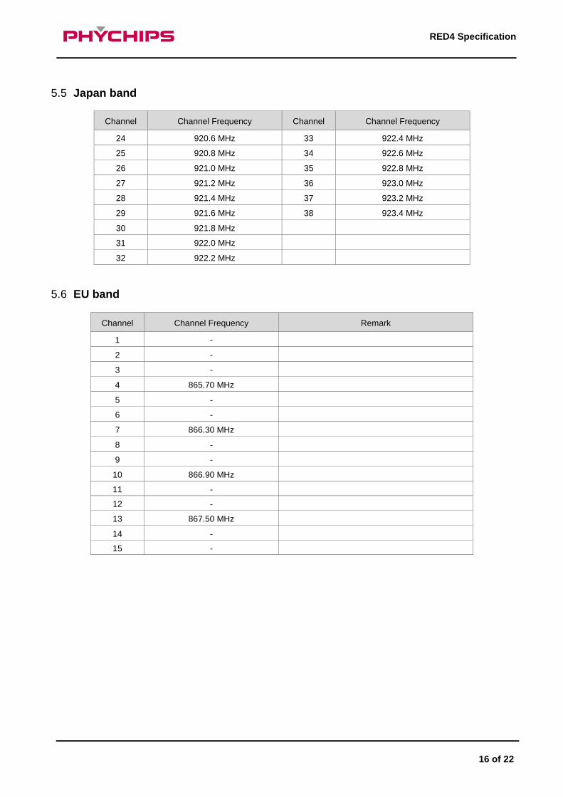
5.5 Japan band
Channel Channel Frequency Channel Channel Frequency
24 920.6 MHz 33 922.4 MHz
25 920.8 MHz 34 922.6 MHz
26 921.0 MHz 35 922.8 MHz
27 921.2 MHz 36 923.0 MHz
28 921.4 MHz 37 923.2 MHz
29 921.6 MHz 38 923.4 MHz
30 921.8 MHz
31 922.0 MHz
32 922.2 MHz
5.6 EU band
Channel Channel Frequency Remark
1 -
2 -
3 -
4 865.70 MHz
5 -
6 -
7 866.30 MHz
8 -
9 -
10 866.90 MHz
11 -
12 -
13 867.50 MHz
14 -
15 -
17 of 22
RED4 Specification
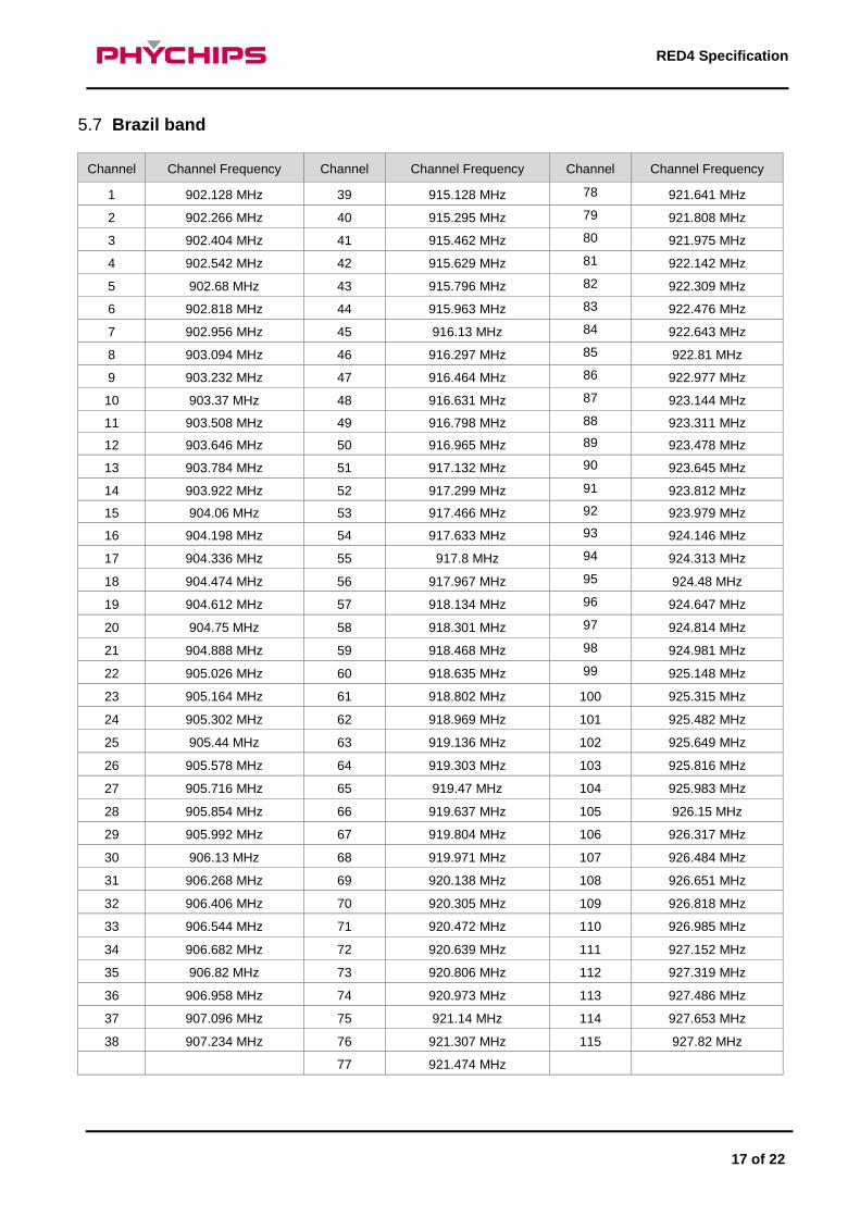
5.7 Brazil band
Channel Channel Frequency Channel Channel Frequency Channel Channel Frequency
1 902.128 MHz 39 915.128 MHz 78 921.641 MHz
2 902.266 MHz 40 915.295 MHz 79 921.808 MHz
3 902.404 MHz 41 915.462 MHz 80 921.975 MHz
4 902.542 MHz 42 915.629 MHz 81 922.142 MHz
5 902.68 MHz 43 915.796 MHz 82 922.309 MHz
6 902.818 MHz 44 915.963 MHz 83 922.476 MHz
7 902.956 MHz 45 916.13 MHz 84 922.643 MHz
8 903.094 MHz 46 916.297 MHz 85 922.81 MHz
9 903.232 MHz 47 916.464 MHz 86 922.977 MHz
10 903.37 MHz 48 916.631 MHz 87 923.144 MHz
11 903.508 MHz 49 916.798 MHz 88 923.311 MHz
12 903.646 MHz 50 916.965 MHz 89 923.478 MHz
13 903.784 MHz 51 917.132 MHz 90 923.645 MHz
14 903.922 MHz 52 917.299 MHz 91 923.812 MHz
15 904.06 MHz 53 917.466 MHz 92 923.979 MHz
16 904.198 MHz 54 917.633 MHz 93 924.146 MHz
17 904.336 MHz 55 917.8 MHz 94 924.313 MHz
18 904.474 MHz 56 917.967 MHz 95 924.48 MHz
19 904.612 MHz 57 918.134 MHz 96 924.647 MHz
20 904.75 MHz 58 918.301 MHz 97 924.814 MHz
21 904.888 MHz 59 918.468 MHz 98 924.981 MHz
22 905.026 MHz 60 918.635 MHz 99 925.148 MHz
23 905.164 MHz 61 918.802 MHz 100 925.315 MHz
24 905.302 MHz 62 918.969 MHz 101 925.482 MHz
25 905.44 MHz 63 919.136 MHz 102 925.649 MHz
26 905.578 MHz 64 919.303 MHz 103 925.816 MHz
27 905.716 MHz 65 919.47 MHz 104 925.983 MHz
28 905.854 MHz 66 919.637 MHz 105 926.15 MHz
29 905.992 MHz 67 919.804 MHz 106 926.317 MHz
30 906.13 MHz 68 919.971 MHz 107 926.484 MHz
31 906.268 MHz 69 920.138 MHz 108 926.651 MHz
32 906.406 MHz 70 920.305 MHz 109 926.818 MHz
33 906.544 MHz 71 920.472 MHz 110 926.985 MHz
34 906.682 MHz 72 920.639 MHz 111 927.152 MHz
35 906.82 MHz 73 920.806 MHz 112 927.319 MHz
36 906.958 MHz 74 920.973 MHz 113 927.486 MHz
37 907.096 MHz 75 921.14 MHz 114 927.653 MHz
38 907.234 MHz 76 921.307 MHz 115 927.82 MHz
77 921.474 MHz
18 of 22
RED4 Specification
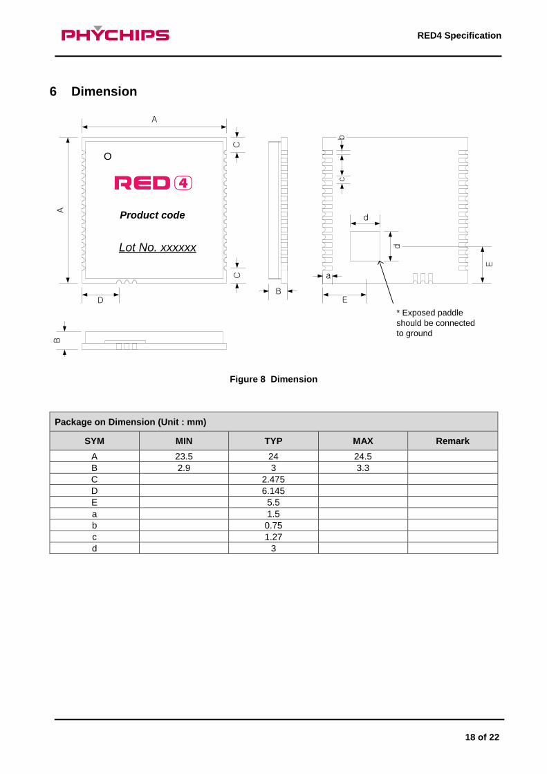
6 Dimension
A
AB
CC
D E
E
bc
a
d
d
B
O
Product code
Lot No. xxxxxx
* Exposed paddle
should be connected
to ground
Figure 8 Dimension
Package on Dimension (Unit : mm)
SYM MIN TYP MAX Remark
A 23.5 24 24.5
B 2.9 3 3.3
C 2.475
D 6.145
E 5.5
a 1.5
b 0.75
c 1.27
d 3
19 of 22
RED4 Specification
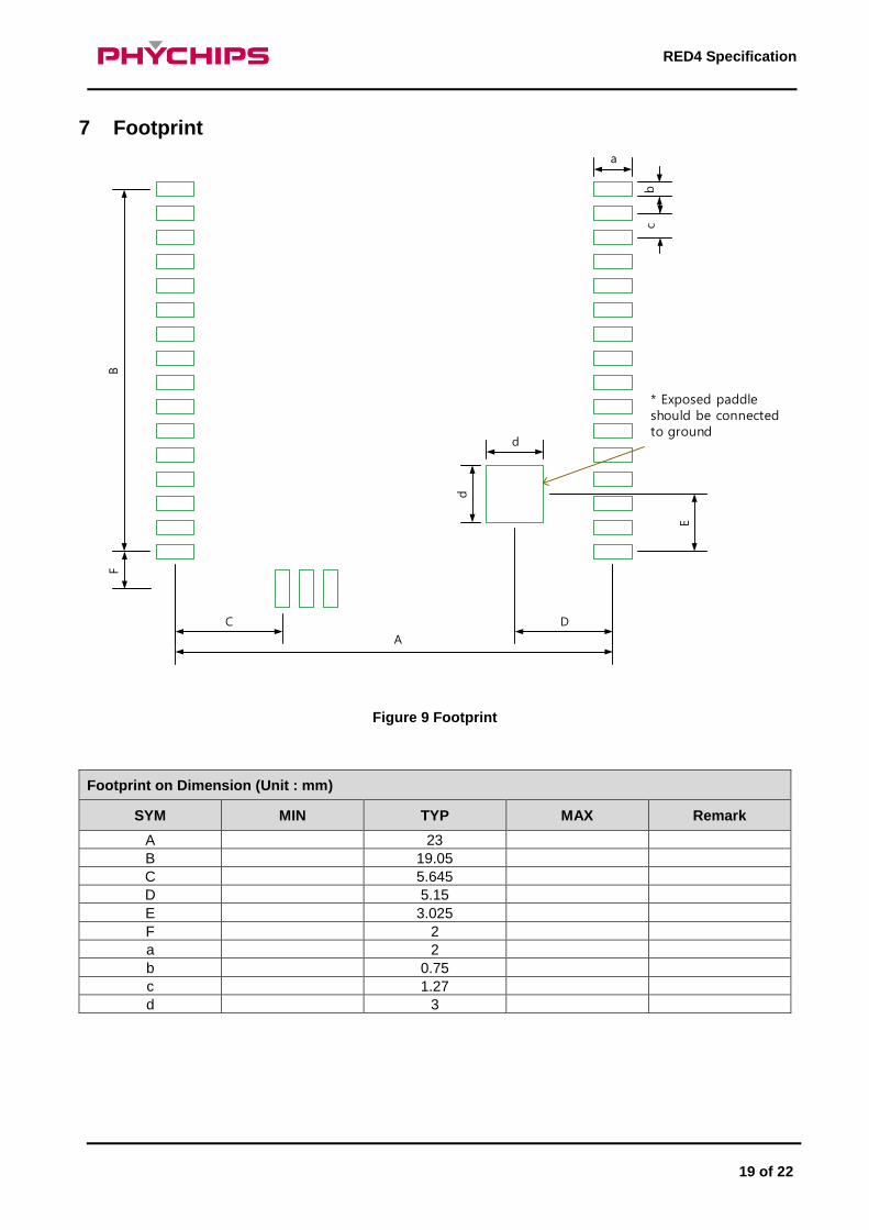
7 Footprint
C D
A
E
d
d
a
bc
BF
* Exposed paddle should be connected to ground
Figure 9 Footprint
Footprint on Dimension (Unit : mm)
SYM MIN TYP MAX Remark
A 23
B 19.05
C 5.645
D 5.15
E 3.025
F 2
a 2
b 0.75
c 1.27
d 3

20 of 22
RED4 Specification
8 Packing Information Packing materials for the RED4 shipment consist of the anti-static inner foam sheets and the outer box which
can hold up to a hundred pieces of the RED4 each box.
8.1 Inner foam sheet dimension Dimension of the inner foam sheet to store the RED4, which can hold up to 20 pcs of the RED4, is approximately
measured to W = 240mm, L = 200mm, H = 10mm. Inner foam sheet helps to avoid both interference between
the products and static from the outside. Detailed shape refer to figure 10 as below.
8.2 Outer box dimension The outer box is made printed card board, which may avoid dust, moisture and shock from the outside and
convenient to ship. Dimension of the outer box is approximately measured to W = 250mm, L = 205mm, H =
75mm. Detailed shape refer to figure 11 as below.
Figure 10 Dimension of the inner foam sheet Figure 11 Dimension of the outer box
※ Packing materials are able to change dimension larger or smaller according to shipped quantity of
mass product or/and internal policies so that shipment can be controlled easily and safely.
21 of 22
RED4 Specification
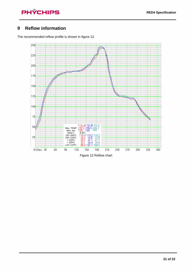
9 Reflow information
The recommended reflow profile is shown in figure 12.
Max. TEMPMax. secDelta T
150~200ºC200~218ºC
> 218ºC > 220ºC
Low~110ºC
Figure 12 Reflow chart
22 of 22
RED4 Specification
10 Address Information
PHYCHIPS Inc.
#104, 187 Techno-2ro, Yuseong-gu, Daejeon, Korea(Yongsan-dong, Migun Technoworld 2), 305-500
http://www.phychips.com
Tel: +82-42-864-2402
Fax: +82-42-864-2403
Disclaimer: PHYCHIPS reserves the right to make changes to the information in this document without prior
notice. The purchase of PHYCHIPS products does not convey any license under patent rights owned by
PHYCHIPS or others. PHYCHIPS does not assume any responsibility for the use of this product. It is the
customer’s responsibility to make sure that the system complies with regulations.
© 2015 PHYCHIPS Inc. All rights reserved. The reproduction of this document is NOT allowed without
approval of PHYCHIPS Inc.


![[PPT]UART and UART Driver - University at Buffalobina/cse321/fall2009/UARTDriver.ppt · Web viewUART and UART Driver B. Ramamurthy * UART UART: Universal Asynchronous Receiver/Transmitter](https://img.pdfslide.net/doc/110x75/5b2ab3637f8b9a55068b752f/pptuart-and-uart-driver-university-at-binacse321fall2009uartdriverppt.jpg)


![[Codientu.org] Uart](https://img.pdfslide.net/doc/110x75/55cf9ad7550346d033a3a8db/codientuorg-uart.jpg)

