Embed Size (px)
Citation preview
7C
6C
5C
4C
3C
2C
1C
COM
7
6
5
4
3
2
1
7B
6B
5B
4B
3B
2B
1B
10
11
12
13
14
15
16
9
Product
Folder
Sample &Buy
Technical
Documents
Tools &
Software
Support &Community
An IMPORTANT NOTICE at the end of this data sheet addresses availability, warranty, changes, use in safety-critical applications,intellectual property matters and other important disclaimers. PRODUCTION DATA.
ULN2002A, ULN2003A, ULN2003AIULQ2003A, ULN2004A, ULQ2004A
SLRS027O –DECEMBER 1976–REVISED JANUARY 2016
ULN200x, ULQ200x High-Voltage, High-Current Darlington Transistor Arrays
1
1 Features1• 500-mA-Rated Collector Current (Single Output)• High-Voltage Outputs: 50 V• Output Clamp Diodes• Inputs Compatible With Various Types of Logic• Relay-Driver Applications
2 Applications• Relay Drivers• Stepper and DC Brushed Motor Drivers• Lamp Drivers• Display Drivers (LED and Gas Discharge)• Line Drivers• Logic Buffers
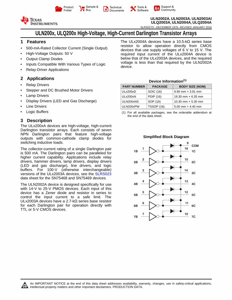
3 DescriptionThe ULx200xA devices are high-voltage, high-currentDarlington transistor arrays. Each consists of sevenNPN Darlington pairs that feature high-voltageoutputs with common-cathode clamp diodes forswitching inductive loads.
The collector-current rating of a single Darlington pairis 500 mA. The Darlington pairs can be paralleled forhigher current capability. Applications include relaydrivers, hammer drivers, lamp drivers, display drivers(LED and gas discharge), line drivers, and logicbuffers. For 100-V (otherwise interchangeable)versions of the ULx2003A devices, see the SLRS023data sheet for the SN75468 and SN75469 devices.
The ULN2002A device is designed specifically for usewith 14-V to 25-V PMOS devices. Each input of thisdevice has a Zener diode and resistor in series tocontrol the input current to a safe limit. TheULx2003A devices have a 2.7-kΩ series base resistorfor each Darlington pair for operation directly withTTL or 5-V CMOS devices.
The ULx2004A devices have a 10.5-kΩ series baseresistor to allow operation directly from CMOSdevices that use supply voltages of 6 V to 15 V. Therequired input current of the ULx2004A device isbelow that of the ULx2003A devices, and the requiredvoltage is less than that required by the ULN2002Adevice.
.
Device Information(1)
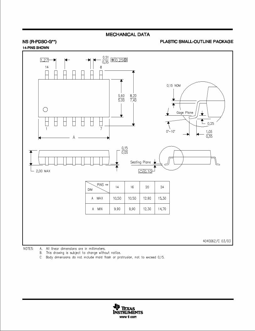
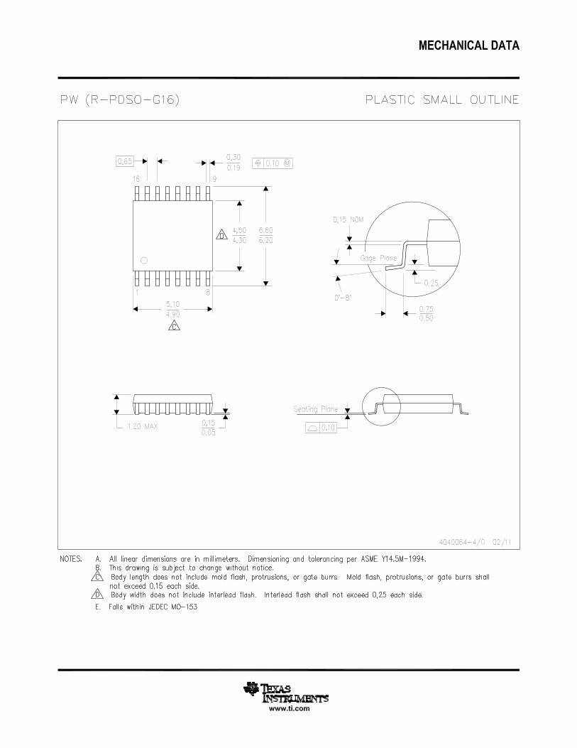
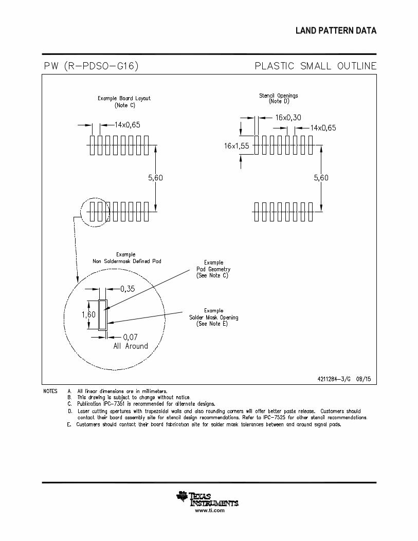
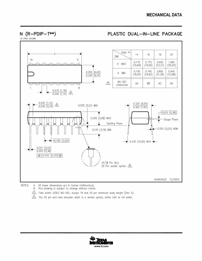
PART NUMBER PACKAGE BODY SIZE (NOM)ULx200xD SOIC (16) 9.90 mm × 3.91 mmULx200xN PDIP (16) 19.30 mm × 6.35 mmULN200xNS SOP (16) 10.30 mm × 5.30 mmULN200xPW TSSOP (16) 5.00 mm × 4.40 mm
(1) For all available packages, see the orderable addendum atthe end of the data sheet.
.
.
Simplified Block Diagram
2
ULN2002A, ULN2003A, ULN2003AIULQ2003A, ULN2004A, ULQ2004ASLRS027O –DECEMBER 1976–REVISED JANUARY 2016 www.ti.com
Product Folder Links: ULN2002A ULN2003A ULN2003AI ULQ2003A ULN2004A ULQ2004A
Submit Documentation Feedback Copyright © 1976–2016, Texas Instruments Incorporated
Table of Contents1 Features .................................................................. 12 Applications ........................................................... 13 Description ............................................................. 14 Revision History..................................................... 25 Pin Configuration and Functions ......................... 36 Specifications......................................................... 4
6.1 Absolute Maximum Ratings ...................................... 46.2 ESD Ratings.............................................................. 46.3 Recommended Operating Conditions....................... 46.4 Thermal Information .................................................. 46.5 Electrical Characteristics: ULN2002A ....................... 56.6 Electrical Characteristics: ULN2003A and
ULN2004A.................................................................. 56.7 Electrical Characteristics: ULN2003AI ...................... 66.8 Electrical Characteristics: ULN2003AI ..................... 66.9 Electrical Characteristics: ULQ2003A and
ULQ2004A ................................................................. 76.10 Switching Characteristics: ULN2002A, ULN2003A,
ULN2004A.................................................................. 76.11 Switching Characteristics: ULN2003AI .................. 76.12 Switching Characteristics: ULN2003AI .................. 86.13 Switching Characteristics: ULQ2003A, ULQ2004A 86.14 Typical Characteristics ............................................ 8
7 Parameter Measurement Information ................ 108 Detailed Description ............................................ 12
8.1 Overview ................................................................. 128.2 Functional Block Diagrams ..................................... 128.3 Feature Description................................................. 138.4 Device Functional Modes........................................ 13
9 Application and Implementation ........................ 149.1 Application Information............................................ 149.2 Typical Application ................................................. 149.3 System Examples ................................................... 17
10 Power Supply Recommendations ..................... 1811 Layout................................................................... 18
11.1 Layout Guidelines ................................................. 1811.2 Layout Example .................................................... 18
12 Device and Documentation Support ................. 1912.1 Documentation Support ........................................ 1912.2 Related Links ........................................................ 1912.3 Community Resources.......................................... 1912.4 Trademarks ........................................................... 1912.5 Electrostatic Discharge Caution............................ 1912.6 Glossary ................................................................ 19
13 Mechanical, Packaging, and OrderableInformation ........................................................... 19
4 Revision HistoryNOTE: Page numbers for previous revisions may differ from page numbers in the current version.
Changes from Revision N (June 2015) to Revision O Page
• Changed Pin Functions table to correct typographical error. ................................................................................................ 3
Changes from Revision M (February 2013) to Revision N Page
• Added Pin Configuration and Functions section, ESD Ratings table, Feature Description section, Device FunctionalModes, Application and Implementation section, Power Supply Recommendations section, Layout section, Deviceand Documentation Support section, and Mechanical, Packaging, and Orderable Information section .............................. 1
• Deleted Ordering Information table. No specification changes. ............................................................................................. 1• Moved Typical Characteristics into Specifications section. ................................................................................................... 8
Changes from Revision L (April 2012) to Revision M Page
• Updated temperature rating for ULN2003AI in the ORDERING INFORMATION table ........................................................ 1
Changes from Revision K (August 2011) to Revision L Page
• Removed reference to obsolete ULN2001 device.................................................................................................................. 1
1B 1 16
2B 2 15
3B 3 14
4B 4 13
5B 5 12
6B 6 11
7B 7 10
E 8 9
1C
2C
3C
4C
5C
6C
7C
COM
3
ULN2002A, ULN2003A, ULN2003AIULQ2003A, ULN2004A, ULQ2004A
www.ti.com SLRS027O –DECEMBER 1976–REVISED JANUARY 2016
Product Folder Links: ULN2002A ULN2003A ULN2003AI ULQ2003A ULN2004A ULQ2004A
Submit Documentation FeedbackCopyright © 1976–2016, Texas Instruments Incorporated
(1) I = Input, O = Output
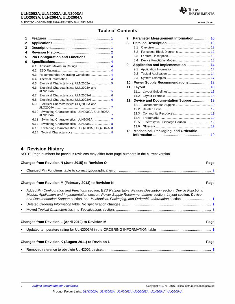
5 Pin Configuration and Functions
D, N, NS, and PW Package16-Pin SOIC, PDIP, SO, and TSSOP
Top View
Pin FunctionsPIN
I/O (1) DESCRIPTIONNAME NO.1B 1
I Channel 1 through 7 Darlington base input
2B 23B 34B 45B 56B 67B 71C 16
O Channel 1 through 7 Darlington collector output
2C 153C 144C 135C 126C 117C 10COM 9 — Common cathode node for flyback diodes (required for inductive loads)E 8 — Common emitter shared by all channels (typically tied to ground)
4
ULN2002A, ULN2003A, ULN2003AIULQ2003A, ULN2004A, ULQ2004ASLRS027O –DECEMBER 1976–REVISED JANUARY 2016 www.ti.com
Product Folder Links: ULN2002A ULN2003A ULN2003AI ULQ2003A ULN2004A ULQ2004A
Submit Documentation Feedback Copyright © 1976–2016, Texas Instruments Incorporated
(1) Stresses beyond those listed under Absolute Maximum Ratings may cause permanent damage to the device. These are stress ratingsonly, and functional operation of the device at these or any other conditions beyond those indicated under Recommended OperatingConditions is not implied. Exposure to absolute-maximum-rated conditions for extended periods may affect device reliability.
(2) All voltage values are with respect to the emitter/substrate terminal E, unless otherwise noted.
6 Specifications
6.1 Absolute Maximum Ratingsat 25°C free-air temperature (unless otherwise noted) (1)
MIN MAX UNITVCC Collector-emitter voltage 50 V
Clamp diode reverse voltage (2) 50 VVI Input voltage (2) 30 V
Peak collector current, See Figure 4 and Figure 5 500 mAIOK Output clamp current 500 mA
Total emitter-terminal current –2.5 A
TA Operating free-air temperature range
ULN200xA –20 70
°CULN200xAI –40 105ULQ200xA –40 85ULQ200xAT –40 105
TJ Operating virtual junction temperature 150 °CLead temperature for 1.6 mm (1/16 inch) from case for 10 seconds 260 °C
Tstg Storage temperature –65 150 °C
(1) JEDEC document JEP155 states that 500-V HBM allows safe manufacturing with a standard ESD control process.(2) JEDEC document JEP157 states that 250-V CDM allows safe manufacturing with a standard ESD control process.
6.2 ESD RatingsVALUE UNIT
V(ESD)Electrostaticdischarge
Human body model (HBM), per ANSI/ESDA/JEDEC JS-001 (1) ±2000V
Charged device model (CDM), per JEDEC specification JESD22-C101 (2) ±500
6.3 Recommended Operating Conditionsover operating free-air temperature range (unless otherwise noted)
MIN MAX UNITVCC Collector-emitter voltage (non-V devices) 0 50 VTJ Junction temperature –40 125 °C
(1) For more information about traditional and new thermal metrics, see the Semiconductor and IC Package Thermal Metrics applicationreport, SPRA953.
6.4 Thermal Information
THERMAL METRIC (1)
ULx200x
UNITD(SOIC)
N(PDIP)
NS(SO)
PW(TSSOP)
16 PINS 16 PINS 16 PINS 16 PINSRθJA Junction-to-ambient thermal resistance 73 67 64 108 °C/WRθJC(top) Junction-to-case (top) thermal resistance 36 54 n/a 33.6 °C/WRθJB Junction-to-board thermal resistance n/a n/a n/a 51.9 °C/WψJT Junction-to-top characterization parameter n/a n/a n/a 2.1 °C/WψJB Junction-to-board characterization parameter n/a n/a n/a 51.4 °C/W
5
ULN2002A, ULN2003A, ULN2003AIULQ2003A, ULN2004A, ULQ2004A
www.ti.com SLRS027O –DECEMBER 1976–REVISED JANUARY 2016
Product Folder Links: ULN2002A ULN2003A ULN2003AI ULQ2003A ULN2004A ULQ2004A
Submit Documentation FeedbackCopyright © 1976–2016, Texas Instruments Incorporated
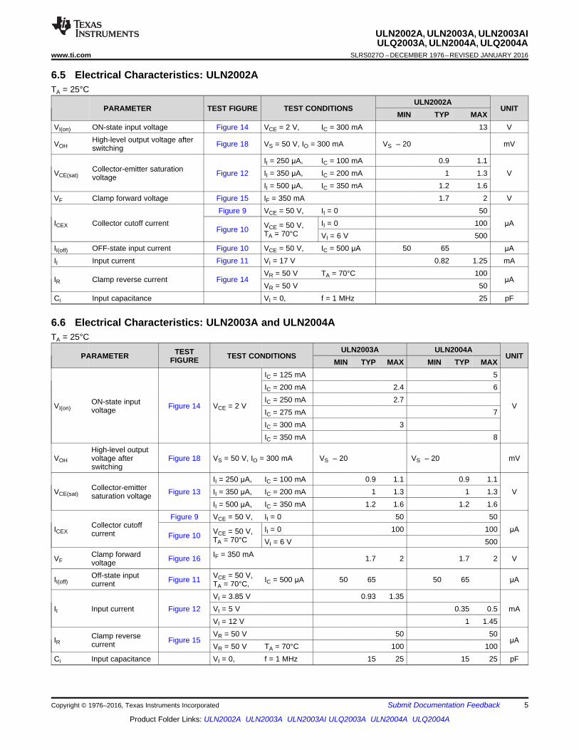
6.5 Electrical Characteristics: ULN2002ATA = 25°C
PARAMETER TEST FIGURE TEST CONDITIONSULN2002A
UNITMIN TYP MAX
VI(on) ON-state input voltage Figure 14 VCE = 2 V, IC = 300 mA 13 V
VOHHigh-level output voltage afterswitching Figure 18 VS = 50 V, IO = 300 mA VS – 20 mV
VCE(sat)Collector-emitter saturationvoltage Figure 12
II = 250 μA, IC = 100 mA 0.9 1.1VII = 350 μA, IC = 200 mA 1 1.3
II = 500 μA, IC = 350 mA 1.2 1.6VF Clamp forward voltage Figure 15 IF = 350 mA 1.7 2 V
ICEX Collector cutoff currentFigure 9 VCE = 50 V, II = 0 50
μAFigure 10 VCE = 50 V,
TA = 70°CII = 0 100VI = 6 V 500
II(off) OFF-state input current Figure 10 VCE = 50 V, IC = 500 μA 50 65 μAII Input current Figure 11 VI = 17 V 0.82 1.25 mA
IR Clamp reverse current Figure 14VR = 50 V TA = 70°C 100
μAVR = 50 V 50
Ci Input capacitance VI = 0, f = 1 MHz 25 pF
6.6 Electrical Characteristics: ULN2003A and ULN2004ATA = 25°C
PARAMETER TESTFIGURE TEST CONDITIONS
ULN2003A ULN2004AUNIT
MIN TYP MAX MIN TYP MAX
VI(on)ON-state inputvoltage Figure 14 VCE = 2 V
IC = 125 mA 5
V
IC = 200 mA 2.4 6IC = 250 mA 2.7IC = 275 mA 7IC = 300 mA 3IC = 350 mA 8
VOH
High-level outputvoltage afterswitching
Figure 18 VS = 50 V, IO = 300 mA VS – 20 VS – 20 mV
VCE(sat)Collector-emittersaturation voltage Figure 13
II = 250 μA, IC = 100 mA 0.9 1.1 0.9 1.1VII = 350 μA, IC = 200 mA 1 1.3 1 1.3
II = 500 μA, IC = 350 mA 1.2 1.6 1.2 1.6
ICEXCollector cutoffcurrent
Figure 9 VCE = 50 V, II = 0 50 50μA
Figure 10 VCE = 50 V,TA = 70°C
II = 0 100 100VI = 6 V 500
VFClamp forwardvoltage Figure 16 IF = 350 mA 1.7 2 1.7 2 V
II(off)Off-state inputcurrent Figure 11 VCE = 50 V,
TA = 70°C, IC = 500 μA 50 65 50 65 μA
II Input current Figure 12VI = 3.85 V 0.93 1.35
mAVI = 5 V 0.35 0.5VI = 12 V 1 1.45
IRClamp reversecurrent Figure 15
VR = 50 V 50 50μA
VR = 50 V TA = 70°C 100 100Ci Input capacitance VI = 0, f = 1 MHz 15 25 15 25 pF
6
ULN2002A, ULN2003A, ULN2003AIULQ2003A, ULN2004A, ULQ2004ASLRS027O –DECEMBER 1976–REVISED JANUARY 2016 www.ti.com
Product Folder Links: ULN2002A ULN2003A ULN2003AI ULQ2003A ULN2004A ULQ2004A
Submit Documentation Feedback Copyright © 1976–2016, Texas Instruments Incorporated
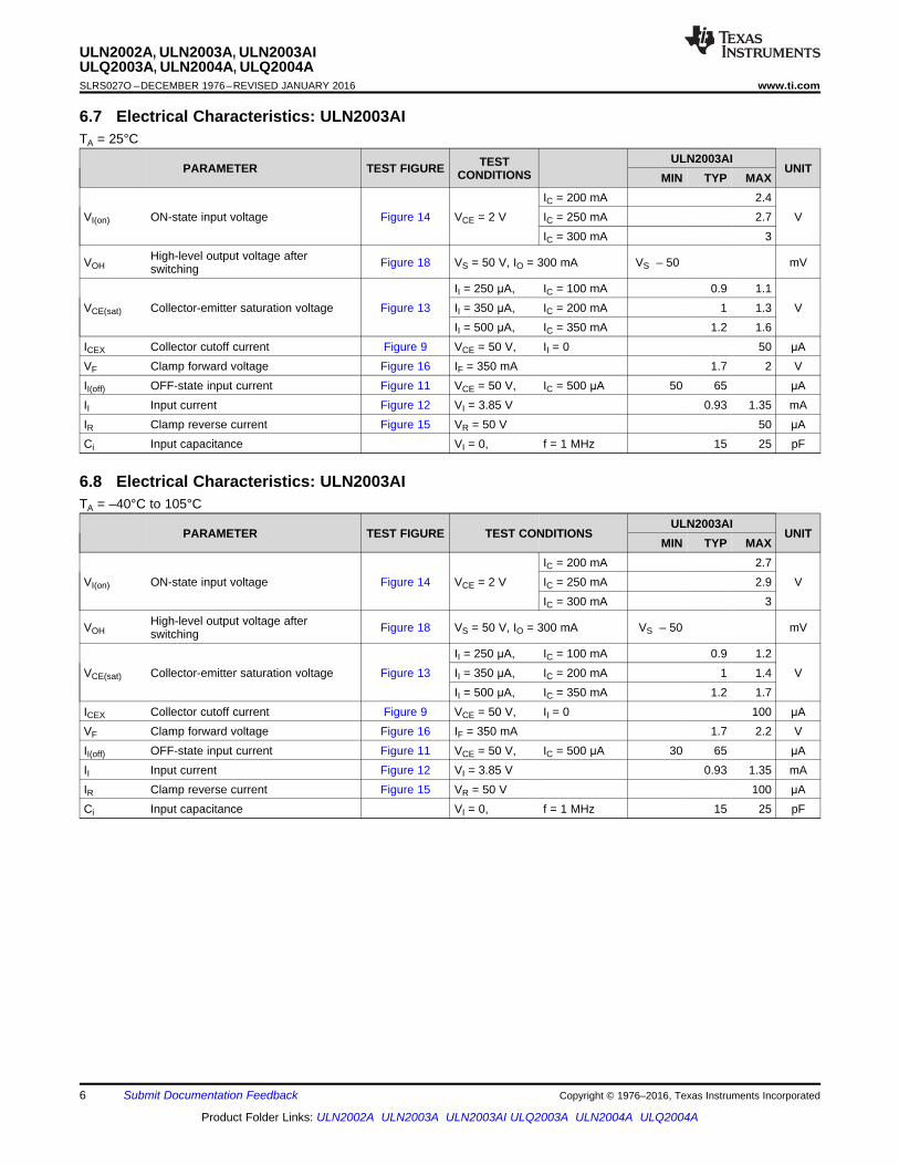
6.7 Electrical Characteristics: ULN2003AITA = 25°C
PARAMETER TEST FIGURE TESTCONDITIONS
ULN2003AIUNIT
MIN TYP MAX
VI(on) ON-state input voltage Figure 14 VCE = 2 VIC = 200 mA 2.4
VIC = 250 mA 2.7IC = 300 mA 3
VOHHigh-level output voltage afterswitching Figure 18 VS = 50 V, IO = 300 mA VS – 50 mV
VCE(sat) Collector-emitter saturation voltage Figure 13II = 250 μA, IC = 100 mA 0.9 1.1
VII = 350 μA, IC = 200 mA 1 1.3II = 500 μA, IC = 350 mA 1.2 1.6
ICEX Collector cutoff current Figure 9 VCE = 50 V, II = 0 50 μAVF Clamp forward voltage Figure 16 IF = 350 mA 1.7 2 VII(off) OFF-state input current Figure 11 VCE = 50 V, IC = 500 μA 50 65 μAII Input current Figure 12 VI = 3.85 V 0.93 1.35 mAIR Clamp reverse current Figure 15 VR = 50 V 50 μACi Input capacitance VI = 0, f = 1 MHz 15 25 pF
6.8 Electrical Characteristics: ULN2003AITA = –40°C to 105°C
PARAMETER TEST FIGURE TEST CONDITIONSULN2003AI
UNITMIN TYP MAX
VI(on) ON-state input voltage Figure 14 VCE = 2 VIC = 200 mA 2.7
VIC = 250 mA 2.9IC = 300 mA 3
VOHHigh-level output voltage afterswitching Figure 18 VS = 50 V, IO = 300 mA VS – 50 mV
VCE(sat) Collector-emitter saturation voltage Figure 13II = 250 μA, IC = 100 mA 0.9 1.2
VII = 350 μA, IC = 200 mA 1 1.4II = 500 μA, IC = 350 mA 1.2 1.7
ICEX Collector cutoff current Figure 9 VCE = 50 V, II = 0 100 μAVF Clamp forward voltage Figure 16 IF = 350 mA 1.7 2.2 VII(off) OFF-state input current Figure 11 VCE = 50 V, IC = 500 μA 30 65 μAII Input current Figure 12 VI = 3.85 V 0.93 1.35 mAIR Clamp reverse current Figure 15 VR = 50 V 100 μACi Input capacitance VI = 0, f = 1 MHz 15 25 pF
7
ULN2002A, ULN2003A, ULN2003AIULQ2003A, ULN2004A, ULQ2004A
www.ti.com SLRS027O –DECEMBER 1976–REVISED JANUARY 2016
Product Folder Links: ULN2002A ULN2003A ULN2003AI ULQ2003A ULN2004A ULQ2004A
Submit Documentation FeedbackCopyright © 1976–2016, Texas Instruments Incorporated
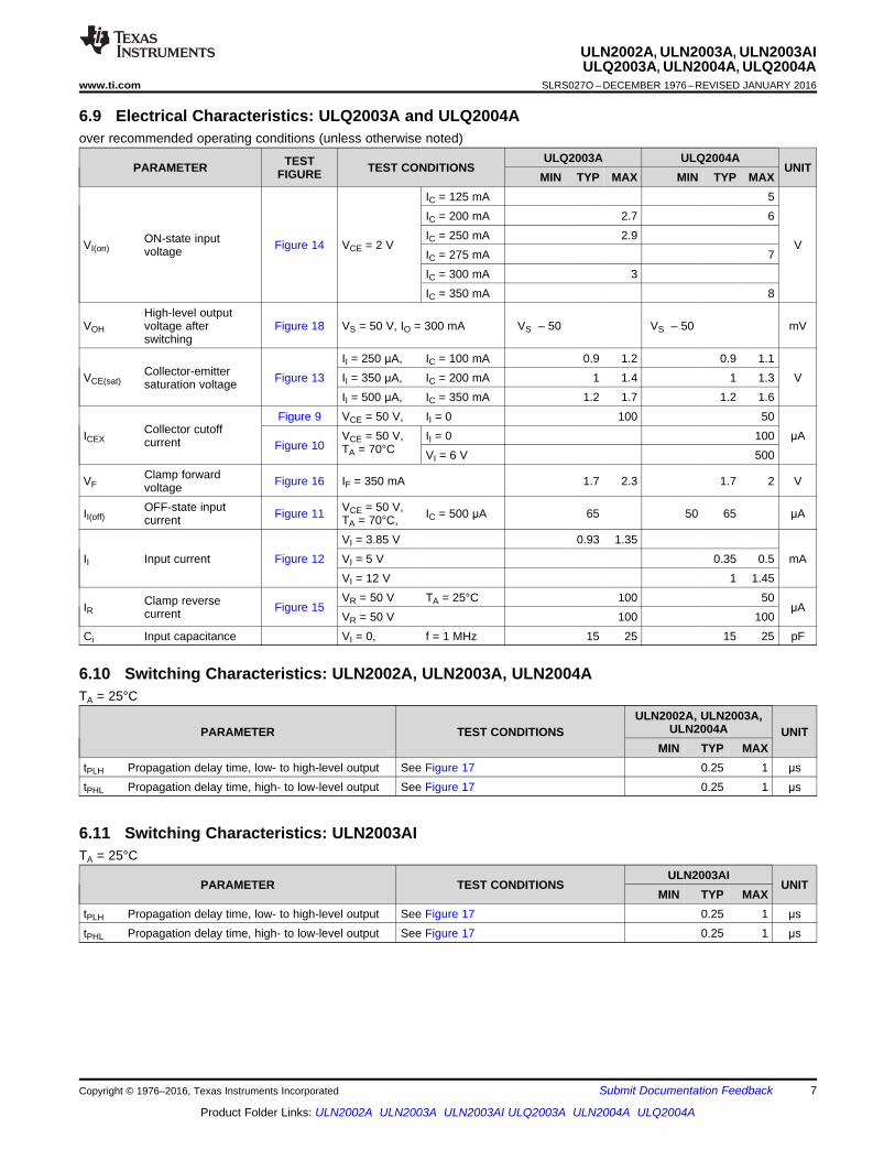
6.9 Electrical Characteristics: ULQ2003A and ULQ2004Aover recommended operating conditions (unless otherwise noted)
PARAMETER TESTFIGURE TEST CONDITIONS
ULQ2003A ULQ2004AUNIT
MIN TYP MAX MIN TYP MAX
VI(on)ON-state inputvoltage Figure 14 VCE = 2 V
IC = 125 mA 5
V
IC = 200 mA 2.7 6IC = 250 mA 2.9IC = 275 mA 7IC = 300 mA 3IC = 350 mA 8
VOH
High-level outputvoltage afterswitching
Figure 18 VS = 50 V, IO = 300 mA VS – 50 VS – 50 mV
VCE(sat)Collector-emittersaturation voltage Figure 13
II = 250 μA, IC = 100 mA 0.9 1.2 0.9 1.1VII = 350 μA, IC = 200 mA 1 1.4 1 1.3
II = 500 μA, IC = 350 mA 1.2 1.7 1.2 1.6
ICEXCollector cutoffcurrent
Figure 9 VCE = 50 V, II = 0 100 50μA
Figure 10VCE = 50 V,TA = 70°C
II = 0 100VI = 6 V 500
VFClamp forwardvoltage Figure 16 IF = 350 mA 1.7 2.3 1.7 2 V
II(off)OFF-state inputcurrent Figure 11 VCE = 50 V,
TA = 70°C, IC = 500 μA 65 50 65 μA
II Input current Figure 12VI = 3.85 V 0.93 1.35
mAVI = 5 V 0.35 0.5VI = 12 V 1 1.45
IRClamp reversecurrent Figure 15
VR = 50 V TA = 25°C 100 50μA
VR = 50 V 100 100Ci Input capacitance VI = 0, f = 1 MHz 15 25 15 25 pF
6.10 Switching Characteristics: ULN2002A, ULN2003A, ULN2004ATA = 25°C
PARAMETER TEST CONDITIONSULN2002A, ULN2003A,
ULN2004A UNITMIN TYP MAX
tPLH Propagation delay time, low- to high-level output See Figure 17 0.25 1 μstPHL Propagation delay time, high- to low-level output See Figure 17 0.25 1 μs
6.11 Switching Characteristics: ULN2003AITA = 25°C
PARAMETER TEST CONDITIONSULN2003AI
UNITMIN TYP MAX
tPLH Propagation delay time, low- to high-level output See Figure 17 0.25 1 μstPHL Propagation delay time, high- to low-level output See Figure 17 0.25 1 μs
2
1.5
1
0.5
7006005004003002001000
800
2.5
IC(tot) - Total Collector Current - mA
0VC
E(s
at)
-C
ollec
tor-
Em
itte
rS
atu
rati
on
Vo
ltag
e-
VV
CE
(sa
t)II = 250 µA
II = 350 µA
II = 500 µA
TA = 25°C
0
IC - Collector Current - mA
2.5
8000
100 200 300 400 500 600 700
0.5
1
1.5
2
II = 350 µA
II = 500 µA
VC
E(s
at)
-C
oll
ec
tor-
Em
itte
rS
atu
rati
on
Vo
ltag
e-
VV
CE
(sa
t)
TA = 25°C
II = 250 µA
8
ULN2002A, ULN2003A, ULN2003AIULQ2003A, ULN2004A, ULQ2004ASLRS027O –DECEMBER 1976–REVISED JANUARY 2016 www.ti.com
Product Folder Links: ULN2002A ULN2003A ULN2003AI ULQ2003A ULN2004A ULQ2004A
Submit Documentation Feedback Copyright © 1976–2016, Texas Instruments Incorporated
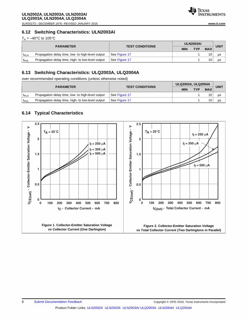
6.12 Switching Characteristics: ULN2003AITA = –40°C to 105°C
PARAMETER TEST CONDITIONSULN2003AI
UNITMIN TYP MAX
tPLH Propagation delay time, low- to high-level output See Figure 17 1 10 μstPHL Propagation delay time, high- to low-level output See Figure 17 1 10 μs
6.13 Switching Characteristics: ULQ2003A, ULQ2004Aover recommended operating conditions (unless otherwise noted)
PARAMETER TEST CONDITIONSULQ2003A, ULQ2004A
UNITMIN TYP MAX
tPLH Propagation delay time, low- to high-level output See Figure 17 1 10 μstPHL Propagation delay time, high- to low-level output See Figure 17 1 10 μs
6.14 Typical Characteristics
Figure 1. Collector-Emitter Saturation Voltagevs Collector Current (One Darlington)
Figure 2. Collector-Emitter Saturation Voltagevs Total Collector Current (Two Darlingtons in Parallel)
0.9
1.1
1.3
1.5
1.7
1.9
2.1
100 200 300 400 500
Output Current – mA
Maxim
um
VC
E(s
at)
Vo
ltag
e –
V
TJ = -40°C to 105°C
Maximum
Typical
100
150
200
250
300
350
400
450
500
250 350 450 550 650
Input Current – µA
Ou
tpu
t C
urr
en
t–
mA
VCE = 2 V
TJ = -40°C to 105°C
Minimum
Conducting SimultaneouslyN = Number of Outputs
500
400
300
200
100
9080706050403020100
100
600
Duty Cycle - %
0
N = 7
TA = 85°C
N = 5
N = 3
N = 2
N = 6
N = 1
IC-
Maxim
um
Co
lle
cto
rC
urr
en
t-
mA
CI
N = 4
0
200
400
600
800
1000
1200
1400
1600
1800
2000
2 2.5 3 3.5 4 4.5 5
Input Voltage – V
Inp
ut
Cu
rren
t – µ
A
TJ = -40°C to 105°C
Maximum
Typical
0
Duty Cycle - %
600
1000
10 20 30 40 50 60 70 80 90
100
200
300
400
500
TA = 70°C
N = Number of OutputsConducting Simultaneously
N = 6N = 7N = 5
N = 3
N = 2
N = 1
IC-
Maxim
um
Co
lle
cto
rC
urr
en
t-
mA
CI
N = 4
0
II - Input Current - µA
500
200
0
25 50 75 100 125 150 175
50
100
150
200
250
300
350
400
450
VS = 10 V
VS = 8 V
IC-
Co
lle
cto
rC
urr
en
t-
mA
CI
RL = 10 Ω
TA = 25°C
9
ULN2002A, ULN2003A, ULN2003AIULQ2003A, ULN2004A, ULQ2004A
www.ti.com SLRS027O –DECEMBER 1976–REVISED JANUARY 2016
Product Folder Links: ULN2002A ULN2003A ULN2003AI ULQ2003A ULN2004A ULQ2004A
Submit Documentation FeedbackCopyright © 1976–2016, Texas Instruments Incorporated
Typical Characteristics (continued)
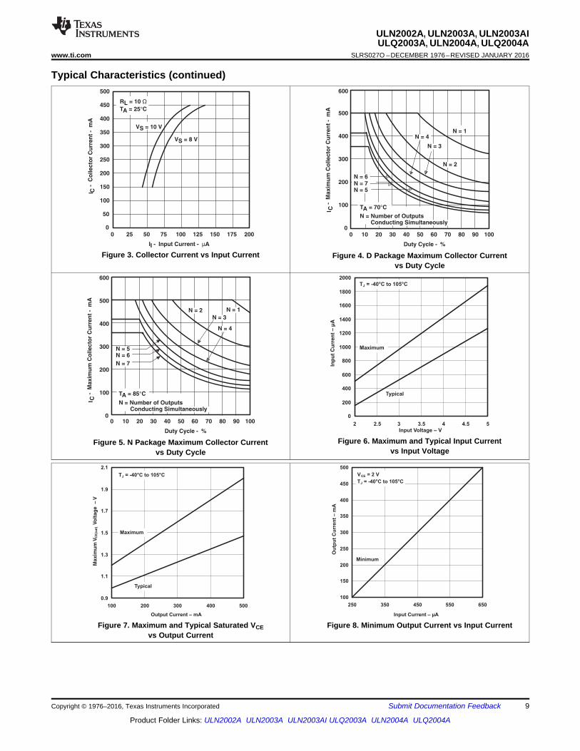
Figure 3. Collector Current vs Input Current Figure 4. D Package Maximum Collector Currentvs Duty Cycle
Figure 5. N Package Maximum Collector Currentvs Duty Cycle
Figure 6. Maximum and Typical Input Currentvs Input Voltage
Figure 7. Maximum and Typical Saturated VCEvs Output Current
Figure 8. Minimum Output Current vs Input Current
Open
VCE ICII
hFE =ICII
Open
VCE ICVI(on)
Open VCE
ICII(off)
Open
Open
II(on)
VI
Open VCE
Open
ICEX
Open VCE
VI
ICEX
10
ULN2002A, ULN2003A, ULN2003AIULQ2003A, ULN2004A, ULQ2004ASLRS027O –DECEMBER 1976–REVISED JANUARY 2016 www.ti.com
Product Folder Links: ULN2002A ULN2003A ULN2003AI ULQ2003A ULN2004A ULQ2004A
Submit Documentation Feedback Copyright © 1976–2016, Texas Instruments Incorporated
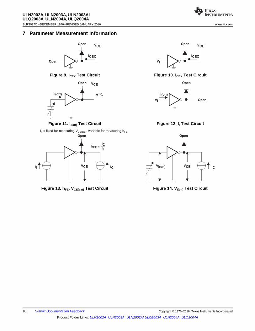
7 Parameter Measurement Information
Figure 9. ICEX Test Circuit Figure 10. ICEX Test Circuit
Figure 11. II(off) Test Circuit Figure 12. II Test CircuitII is fixed for measuring VCE(sat), variable for measuring hFE.
Figure 13. hFE, VCE(sat) Test Circuit Figure 14. VI(on) Test Circuit
90% 90%
1.5 V 1.5 V10% 10%
40 µs
≤10 ns≤5 ns
VIH(see Note C)
0 V
VOH
VOL
Input
Output
VOLTAGE WAVEFORMS
200 W
VR
Open
IR IFVF
Open
11
ULN2002A, ULN2003A, ULN2003AIULQ2003A, ULN2004A, ULQ2004A
www.ti.com SLRS027O –DECEMBER 1976–REVISED JANUARY 2016
Product Folder Links: ULN2002A ULN2003A ULN2003AI ULQ2003A ULN2004A ULQ2004A
Submit Documentation FeedbackCopyright © 1976–2016, Texas Instruments Incorporated
Parameter Measurement Information (continued)
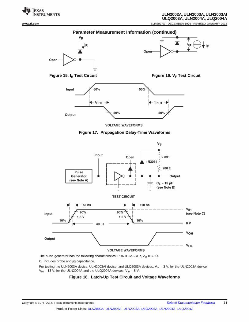
Figure 15. IR Test Circuit Figure 16. VF Test Circuit
Figure 17. Propagation Delay-Time Waveforms
The pulse generator has the following characteristics: PRR = 12.5 kHz, ZO = 50 Ω.CL includes probe and jig capacitance.For testing the ULN2003A device, ULN2003AI device, and ULQ2003A devices, VIH = 3 V; for the ULN2002A device,VIH = 13 V; for the ULN2004A and the ULQ2004A devices, VIH = 8 V.
Figure 18. Latch-Up Test Circuit and Voltage Waveforms
COM
Output C
E
Input B
RB2.7 N
7.2 N 3 N
COM
Output C
E
Input B
RB10.5 N
7.2 N 3 N
COM
Output C
E
Input B10.5 N
7.2 N 3 N
7 V
12
ULN2002A, ULN2003A, ULN2003AIULQ2003A, ULN2004A, ULQ2004ASLRS027O –DECEMBER 1976–REVISED JANUARY 2016 www.ti.com
Product Folder Links: ULN2002A ULN2003A ULN2003AI ULQ2003A ULN2004A ULQ2004A
Submit Documentation Feedback Copyright © 1976–2016, Texas Instruments Incorporated
8 Detailed Description
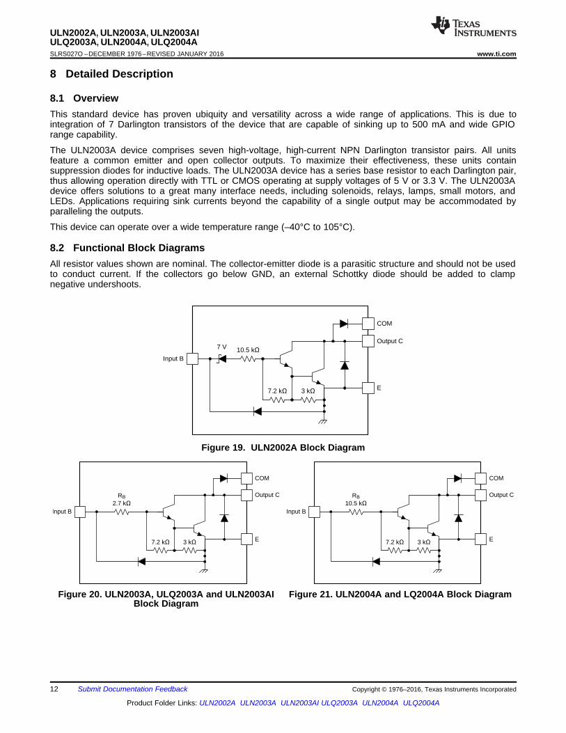
8.1 OverviewThis standard device has proven ubiquity and versatility across a wide range of applications. This is due tointegration of 7 Darlington transistors of the device that are capable of sinking up to 500 mA and wide GPIOrange capability.
The ULN2003A device comprises seven high-voltage, high-current NPN Darlington transistor pairs. All unitsfeature a common emitter and open collector outputs. To maximize their effectiveness, these units containsuppression diodes for inductive loads. The ULN2003A device has a series base resistor to each Darlington pair,thus allowing operation directly with TTL or CMOS operating at supply voltages of 5 V or 3.3 V. The ULN2003Adevice offers solutions to a great many interface needs, including solenoids, relays, lamps, small motors, andLEDs. Applications requiring sink currents beyond the capability of a single output may be accommodated byparalleling the outputs.
This device can operate over a wide temperature range (–40°C to 105°C).
8.2 Functional Block DiagramsAll resistor values shown are nominal. The collector-emitter diode is a parasitic structure and should not be usedto conduct current. If the collectors go below GND, an external Schottky diode should be added to clampnegative undershoots.
Figure 19. ULN2002A Block Diagram
Figure 20. ULN2003A, ULQ2003A and ULN2003AIBlock Diagram
Figure 21. ULN2004A and LQ2004A Block Diagram
13
ULN2002A, ULN2003A, ULN2003AIULQ2003A, ULN2004A, ULQ2004A
www.ti.com SLRS027O –DECEMBER 1976–REVISED JANUARY 2016
Product Folder Links: ULN2002A ULN2003A ULN2003AI ULQ2003A ULN2004A ULQ2004A
Submit Documentation FeedbackCopyright © 1976–2016, Texas Instruments Incorporated
8.3 Feature DescriptionEach channel of the ULN2003A device consists of Darlington connected NPN transistors. This connectioncreates the effect of a single transistor with a very high-current gain (β2). This can be as high as 10,000 A/A atcertain currents. The very high β allows for high-output current drive with a very low input current, essentiallyequating to operation with low GPIO voltages.
The GPIO voltage is converted to base current through the 2.7-kΩ resistor connected between the input andbase of the predriver Darlington NPN. The 7.2-kΩ and 3-kΩ resistors connected between the base and emitter ofeach respective NPN act as pulldowns and suppress the amount of leakage that may occur from the input.
The diodes connected between the output and COM pin is used to suppress the kick-back voltage from aninductive load that is excited when the NPN drivers are turned off (stop sinking) and the stored energy in thecoils causes a reverse current to flow into the coil supply through the kick-back diode.
In normal operation the diodes on base and collector pins to emitter will be reversed biased. If these diodes areforward biased, internal parasitic NPN transistors will draw (a nearly equal) current from other (nearby) devicepins.
8.4 Device Functional Modes
8.4.1 Inductive Load DriveWhen the COM pin is tied to the coil supply voltage, ULN2003A device is able to drive inductive loads andsuppress the kick-back voltage through the internal free-wheeling diodes.
8.4.2 Resistive Load DriveWhen driving a resistive load, a pullup resistor is needed in order for ULN2003A device to sink current and forthere to be a logic high level. The COM pin can be left floating for these applications.
IN1
IN2
ULN2003A
IN3
IN4
OUT1
OUT2
OUT3
OUT4
IN5
IN6
IN7
GND
OUT5
OUT6
OUT7
COM
3.3-V Logic
3.3-V Logic
3.3-V Logic
VSUP
VSUP
14
ULN2002A, ULN2003A, ULN2003AIULQ2003A, ULN2004A, ULQ2004ASLRS027O –DECEMBER 1976–REVISED JANUARY 2016 www.ti.com
Product Folder Links: ULN2002A ULN2003A ULN2003AI ULQ2003A ULN2004A ULQ2004A
Submit Documentation Feedback Copyright © 1976–2016, Texas Instruments Incorporated
9 Application and Implementation
NOTEInformation in the following applications sections is not part of the TI componentspecification, and TI does not warrant its accuracy or completeness. TI’s customers areresponsible for determining suitability of components for their purposes. Customers shouldvalidate and test their design implementation to confirm system functionality.
9.1 Application InformationTypically, the ULN2003A device drives a high-voltage or high-current (or both) peripheral from an MCU or logicdevice that cannot tolerate these conditions. This design is a common application of ULN2003A device, drivinginductive loads. This includes motors, solenoids and relays. Figure 22 shows a model for each load type.
9.2 Typical Application
Figure 22. ULN2003A Device as Inductive Load Driver
9.2.1 Design RequirementsFor this design example, use the parameters listed in Table 1 as the input parameters.
Table 1. Design ParametersDESIGN PARAMETER EXAMPLE VALUE
GPIO voltage 3.3 V or 5 VCoil supply voltage 12 V to 48 VNumber of channels 7
Output current (RCOIL) 20 mA to 300 mA per channelDuty cycle 100%
( )J(MAX) A
(MAX)JA
T TPD
-=
q
N
D OLi Li
i 1
P V I
=
= ´å
15
ULN2002A, ULN2003A, ULN2003AIULQ2003A, ULN2004A, ULQ2004A
www.ti.com SLRS027O –DECEMBER 1976–REVISED JANUARY 2016
Product Folder Links: ULN2002A ULN2003A ULN2003AI ULQ2003A ULN2004A ULQ2004A
Submit Documentation FeedbackCopyright © 1976–2016, Texas Instruments Incorporated
9.2.2 Detailed Design ProcedureWhen using ULN2003A device in a coil driving application, determine the following:• Input voltage range• Temperature range• Output and drive current• Power dissipation
9.2.2.1 Drive CurrentThe coil voltage (VSUP), coil resistance (RCOIL), and low-level output voltage (VCE(SAT) or VOL) determine the coilcurrent.
ICOIL = (VSUP – VCE(SAT)) / RCOIL (1)
9.2.2.2 Low-Level Output VoltageThe low-level output voltage (VOL) is the same as VCE(SAT) and can be determined by, Figure 1, Figure 2, orFigure 7.
9.2.2.3 Power Dissipation and TemperatureThe number of coils driven is dependent on the coil current and on-chip power dissipation. The number of coilsdriven can be determined by Figure 4 or Figure 5.
For a more accurate determination of number of coils possible, use the below equation to calculate ULN2003Adevice on-chip power dissipation PD:
where• N is the number of channels active together• VOLi is the OUTi pin voltage for the load current ILi. This is the same as VCE(SAT) (2)
To ensure reliability of ULN2003A device and the system, the on-chip power dissipation must be lower that orequal to the maximum allowable power dissipation (PD(MAX)) dictated by below equation Equation 3.
where• TJ(max) is the target maximum junction temperature• TA is the operating ambient temperature• RθJA is the package junction to ambient thermal resistance (3)
Limit the die junction temperature of the ULN2003A device to less than 125°C. The IC junction temperature isdirectly proportional to the on-chip power dissipation.
Time (s)
Out
put v
olta
ge -
V
-0.004 0 0.004 0.008 0.012 0.0160
1
2
3
4
5
6
7
8
9
10
11
12
13
D001Time (s)
Out
put v
olta
ge -
V
-0.004 0 0.004 0.008 0.012 0.0160
2
4
6
8
10
12
14
D001
16
ULN2002A, ULN2003A, ULN2003AIULQ2003A, ULN2004A, ULQ2004ASLRS027O –DECEMBER 1976–REVISED JANUARY 2016 www.ti.com
Product Folder Links: ULN2002A ULN2003A ULN2003AI ULQ2003A ULN2004A ULQ2004A
Submit Documentation Feedback Copyright © 1976–2016, Texas Instruments Incorporated
9.2.3 Application CurvesThe characterization data shown in Figure 23 and Figure 24 were generated using the ULN2003A device drivingan OMRON G5NB relay and under the following conditions: VIN = 5 V, VSUP= 12 V, and RCOIL= 2.8 kΩ.
Figure 23. Output Response With Activation of Coil(Turnon)
Figure 24. Output Response With De-activation of Coil(Turnoff)
VCC V
RP
ULQ2003A
1
2
3
4
5
6
9
10
11
12
13
14
15
16
8
TTL
Output
7
VDD VULN2004A
ULQ2004A
1
2
3
4
5
6
9
10
11
12
13
14
15
16
8CMOS
Output
7
1
2
3
4
5
6
7
9
10
11
12
13
14
15
16
8
ULN2002A
P-MOS
Output
VSS VULQ2003A
Lam
TestTTL
Output
VCC V
1
2
3
4
5
6
9
10
11
12
13
14
15
16
8
7
17
ULN2002A, ULN2003A, ULN2003AIULQ2003A, ULN2004A, ULQ2004A
www.ti.com SLRS027O –DECEMBER 1976–REVISED JANUARY 2016
Product Folder Links: ULN2002A ULN2003A ULN2003AI ULQ2003A ULN2004A ULQ2004A
Submit Documentation FeedbackCopyright © 1976–2016, Texas Instruments Incorporated
9.3 System Examples
Figure 25. P-MOS to Load Figure 26. TTL to Load
Figure 27. Buffer for Higher Current Loads Figure 28. Use of Pullup Resistors to IncreaseDrive Current
1
2
3
4
8
VCOM
7
6
5
16
E
9
15
14
13
12
11
10
1B
2B
3B
4B
7B
6B
5B
1C
2C
3C
4C
7C
6C
5C
GND
18
ULN2002A, ULN2003A, ULN2003AIULQ2003A, ULN2004A, ULQ2004ASLRS027O –DECEMBER 1976–REVISED JANUARY 2016 www.ti.com
Product Folder Links: ULN2002A ULN2003A ULN2003AI ULQ2003A ULN2004A ULQ2004A
Submit Documentation Feedback Copyright © 1976–2016, Texas Instruments Incorporated
10 Power Supply RecommendationsThis device does not need a power supply. However, the COM pin is typically tied to the system power supply.When this is the case, it is very important to ensure that the output voltage does not heavily exceed the COM pinvoltage. This discrepancy heavily forward biases the fly-back diodes and causes a large current to flow intoCOM, potentially damaging the on-chip metal or over-heating the device.
11 Layout
11.1 Layout GuidelinesThin traces can be used on the input due to the low-current logic that is typically used to drive ULN2003A device.Take care to separate the input channels as much as possible, as to eliminate crosstalk. TI recommends thicktraces for the output to drive whatever high currents that may be needed. Wire thickness can be determined bythe current density of the trace material and desired drive current.
Because all of the channels currents return to a common emitter, it is best to size that trace width to be verywide. Some applications require up to 2.5 A.
11.2 Layout Example
Figure 29. Package Layout
19
ULN2002A, ULN2003A, ULN2003AIULQ2003A, ULN2004A, ULQ2004A
www.ti.com SLRS027O –DECEMBER 1976–REVISED JANUARY 2016
Product Folder Links: ULN2002A ULN2003A ULN2003AI ULQ2003A ULN2004A ULQ2004A
Submit Documentation FeedbackCopyright © 1976–2016, Texas Instruments Incorporated
12 Device and Documentation Support
12.1 Documentation Support
12.1.1 Related DocumentationFor related documentation, see the following:
SN7546x Darlington Transistor Arrays, SLRS023
12.2 Related LinksThe table below lists quick access links. Categories include technical documents, support and communityresources, tools and software, and quick access to sample or buy.
Table 2. Related Links
PARTS PRODUCT FOLDER SAMPLE & BUY TECHNICALDOCUMENTS
TOOLS &SOFTWARE
SUPPORT &COMMUNITY
ULN2002A Click here Click here Click here Click here Click hereULN2003A Click here Click here Click here Click here Click hereULN2003AI Click here Click here Click here Click here Click hereULN2004A Click here Click here Click here Click here Click hereULQ2003A Click here Click here Click here Click here Click hereULQ2004A Click here Click here Click here Click here Click here
12.3 Community ResourcesThe following links connect to TI community resources. Linked contents are provided "AS IS" by the respectivecontributors. They do not constitute TI specifications and do not necessarily reflect TI's views; see TI's Terms ofUse.
TI E2E™ Online Community TI's Engineer-to-Engineer (E2E) Community. Created to foster collaborationamong engineers. At e2e.ti.com, you can ask questions, share knowledge, explore ideas and helpsolve problems with fellow engineers.
Design Support TI's Design Support Quickly find helpful E2E forums along with design support tools andcontact information for technical support.
12.4 TrademarksE2E is a trademark of Texas Instruments.All other trademarks are the property of their respective owners.
12.5 Electrostatic Discharge CautionThese devices have limited built-in ESD protection. The leads should be shorted together or the device placed in conductive foamduring storage or handling to prevent electrostatic damage to the MOS gates.
12.6 GlossarySLYZ022 — TI Glossary.
This glossary lists and explains terms, acronyms, and definitions.
13 Mechanical, Packaging, and Orderable InformationThe following pages include mechanical packaging and orderable information. This information is the mostcurrent data available for the designated devices. This data is subject to change without notice and revision ofthis document. For browser based versions of this data sheet, refer to the left hand navigation.
PACKAGE OPTION ADDENDUM
www.ti.com 15-Apr-2017
Addendum-Page 1
PACKAGING INFORMATION
Orderable Device Status(1)
Package Type PackageDrawing
Pins PackageQty
Eco Plan(2)
Lead/Ball Finish(6)
MSL Peak Temp(3)
Op Temp (°C) Device Marking(4/5)
Samples
ULN2002AN ACTIVE PDIP N 16 25 Pb-Free(RoHS)
CU NIPDAU N / A for Pkg Type -20 to 70 ULN2002AN
ULN2002ANE4 ACTIVE PDIP N 16 25 Pb-Free(RoHS)
CU NIPDAU N / A for Pkg Type -20 to 70 ULN2002AN
ULN2003AD ACTIVE SOIC D 16 40 Green (RoHS& no Sb/Br)
CU NIPDAU Level-1-260C-UNLIM -20 to 70 ULN2003A
ULN2003ADE4 ACTIVE SOIC D 16 40 Green (RoHS& no Sb/Br)
CU NIPDAU Level-1-260C-UNLIM -20 to 70 ULN2003A
ULN2003ADG4 ACTIVE SOIC D 16 40 Green (RoHS& no Sb/Br)
CU NIPDAU Level-1-260C-UNLIM -20 to 70 ULN2003A
ULN2003ADR ACTIVE SOIC D 16 2500 Green (RoHS& no Sb/Br)
CU NIPDAU | CU SN Level-1-260C-UNLIM -20 to 70 ULN2003A
ULN2003ADRE4 ACTIVE SOIC D 16 2500 Green (RoHS& no Sb/Br)
CU NIPDAU Level-1-260C-UNLIM -20 to 70 ULN2003A
ULN2003ADRG3 ACTIVE SOIC D 16 2500 Green (RoHS& no Sb/Br)
CU SN Level-1-260C-UNLIM -20 to 70 ULN2003A
ULN2003ADRG4 ACTIVE SOIC D 16 2500 Green (RoHS& no Sb/Br)
CU NIPDAU Level-1-260C-UNLIM -20 to 70 ULN2003A
ULN2003AID ACTIVE SOIC D 16 40 Green (RoHS& no Sb/Br)
CU NIPDAU Level-1-260C-UNLIM -40 to 105 ULN2003AI
ULN2003AIDE4 ACTIVE SOIC D 16 40 Green (RoHS& no Sb/Br)
CU NIPDAU Level-1-260C-UNLIM -40 to 105 ULN2003AI
ULN2003AIDG4 ACTIVE SOIC D 16 40 Green (RoHS& no Sb/Br)
CU NIPDAU Level-1-260C-UNLIM -40 to 105 ULN2003AI
ULN2003AIDR ACTIVE SOIC D 16 2500 Green (RoHS& no Sb/Br)
CU NIPDAU | CU SN Level-1-260C-UNLIM -40 to 105 ULN2003AI
ULN2003AIDRE4 ACTIVE SOIC D 16 2500 Green (RoHS& no Sb/Br)
CU NIPDAU Level-1-260C-UNLIM -40 to 105 ULN2003AI
ULN2003AIDRG4 ACTIVE SOIC D 16 2500 Green (RoHS& no Sb/Br)
CU NIPDAU Level-1-260C-UNLIM -40 to 105 ULN2003AI
ULN2003AIN ACTIVE PDIP N 16 25 Pb-Free(RoHS)
CU NIPDAU | CU SN N / A for Pkg Type -40 to 105 ULN2003AIN
ULN2003AINE4 ACTIVE PDIP N 16 25 Pb-Free(RoHS)
CU NIPDAU N / A for Pkg Type -40 to 105 ULN2003AIN
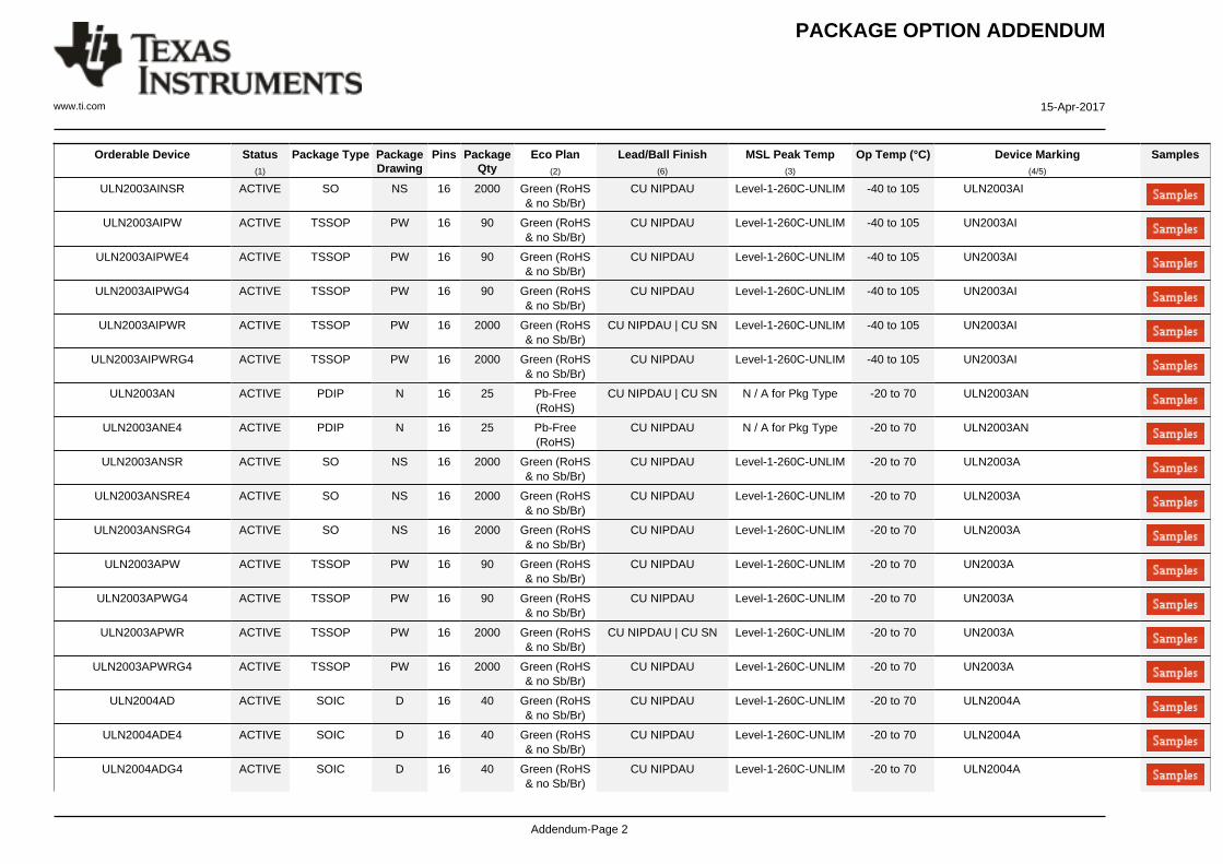
PACKAGE OPTION ADDENDUM
www.ti.com 15-Apr-2017
Addendum-Page 2
Orderable Device Status(1)
Package Type PackageDrawing
Pins PackageQty
Eco Plan(2)
Lead/Ball Finish(6)
MSL Peak Temp(3)
Op Temp (°C) Device Marking(4/5)
Samples
ULN2003AINSR ACTIVE SO NS 16 2000 Green (RoHS& no Sb/Br)
CU NIPDAU Level-1-260C-UNLIM -40 to 105 ULN2003AI
ULN2003AIPW ACTIVE TSSOP PW 16 90 Green (RoHS& no Sb/Br)
CU NIPDAU Level-1-260C-UNLIM -40 to 105 UN2003AI
ULN2003AIPWE4 ACTIVE TSSOP PW 16 90 Green (RoHS& no Sb/Br)
CU NIPDAU Level-1-260C-UNLIM -40 to 105 UN2003AI
ULN2003AIPWG4 ACTIVE TSSOP PW 16 90 Green (RoHS& no Sb/Br)
CU NIPDAU Level-1-260C-UNLIM -40 to 105 UN2003AI
ULN2003AIPWR ACTIVE TSSOP PW 16 2000 Green (RoHS& no Sb/Br)
CU NIPDAU | CU SN Level-1-260C-UNLIM -40 to 105 UN2003AI
ULN2003AIPWRG4 ACTIVE TSSOP PW 16 2000 Green (RoHS& no Sb/Br)
CU NIPDAU Level-1-260C-UNLIM -40 to 105 UN2003AI
ULN2003AN ACTIVE PDIP N 16 25 Pb-Free(RoHS)
CU NIPDAU | CU SN N / A for Pkg Type -20 to 70 ULN2003AN
ULN2003ANE4 ACTIVE PDIP N 16 25 Pb-Free(RoHS)
CU NIPDAU N / A for Pkg Type -20 to 70 ULN2003AN
ULN2003ANSR ACTIVE SO NS 16 2000 Green (RoHS& no Sb/Br)
CU NIPDAU Level-1-260C-UNLIM -20 to 70 ULN2003A
ULN2003ANSRE4 ACTIVE SO NS 16 2000 Green (RoHS& no Sb/Br)
CU NIPDAU Level-1-260C-UNLIM -20 to 70 ULN2003A
ULN2003ANSRG4 ACTIVE SO NS 16 2000 Green (RoHS& no Sb/Br)
CU NIPDAU Level-1-260C-UNLIM -20 to 70 ULN2003A
ULN2003APW ACTIVE TSSOP PW 16 90 Green (RoHS& no Sb/Br)
CU NIPDAU Level-1-260C-UNLIM -20 to 70 UN2003A
ULN2003APWG4 ACTIVE TSSOP PW 16 90 Green (RoHS& no Sb/Br)
CU NIPDAU Level-1-260C-UNLIM -20 to 70 UN2003A
ULN2003APWR ACTIVE TSSOP PW 16 2000 Green (RoHS& no Sb/Br)
CU NIPDAU | CU SN Level-1-260C-UNLIM -20 to 70 UN2003A
ULN2003APWRG4 ACTIVE TSSOP PW 16 2000 Green (RoHS& no Sb/Br)
CU NIPDAU Level-1-260C-UNLIM -20 to 70 UN2003A
ULN2004AD ACTIVE SOIC D 16 40 Green (RoHS& no Sb/Br)
CU NIPDAU Level-1-260C-UNLIM -20 to 70 ULN2004A
ULN2004ADE4 ACTIVE SOIC D 16 40 Green (RoHS& no Sb/Br)
CU NIPDAU Level-1-260C-UNLIM -20 to 70 ULN2004A
ULN2004ADG4 ACTIVE SOIC D 16 40 Green (RoHS& no Sb/Br)
CU NIPDAU Level-1-260C-UNLIM -20 to 70 ULN2004A
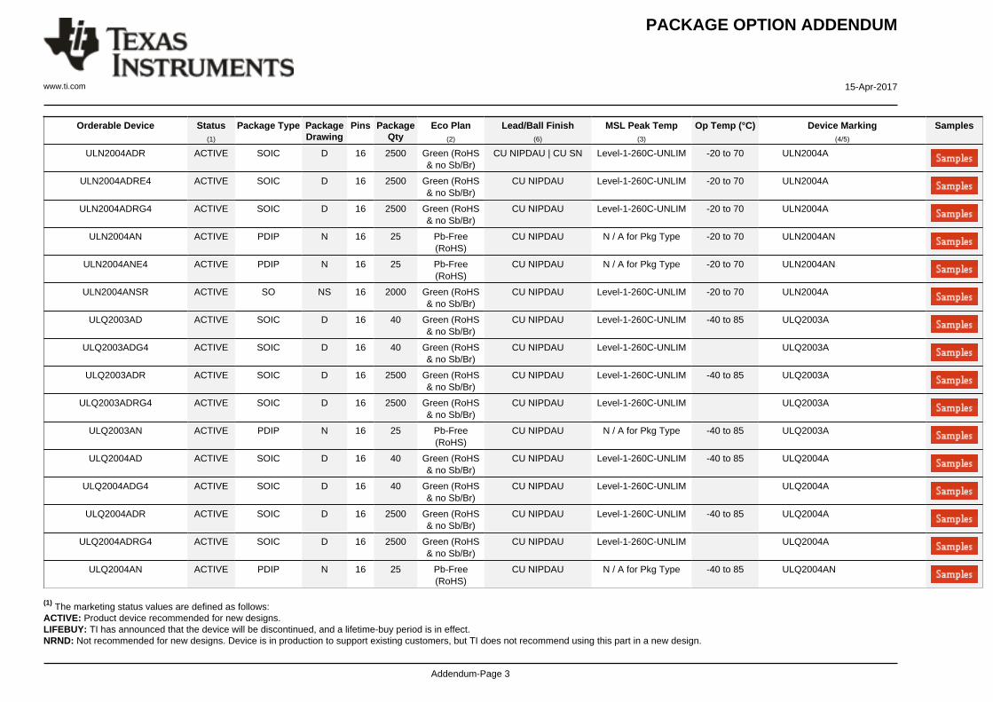
PACKAGE OPTION ADDENDUM
www.ti.com 15-Apr-2017
Addendum-Page 3
Orderable Device Status(1)
Package Type PackageDrawing
Pins PackageQty
Eco Plan(2)
Lead/Ball Finish(6)
MSL Peak Temp(3)
Op Temp (°C) Device Marking(4/5)
Samples
ULN2004ADR ACTIVE SOIC D 16 2500 Green (RoHS& no Sb/Br)
CU NIPDAU | CU SN Level-1-260C-UNLIM -20 to 70 ULN2004A
ULN2004ADRE4 ACTIVE SOIC D 16 2500 Green (RoHS& no Sb/Br)
CU NIPDAU Level-1-260C-UNLIM -20 to 70 ULN2004A
ULN2004ADRG4 ACTIVE SOIC D 16 2500 Green (RoHS& no Sb/Br)
CU NIPDAU Level-1-260C-UNLIM -20 to 70 ULN2004A
ULN2004AN ACTIVE PDIP N 16 25 Pb-Free(RoHS)
CU NIPDAU N / A for Pkg Type -20 to 70 ULN2004AN
ULN2004ANE4 ACTIVE PDIP N 16 25 Pb-Free(RoHS)
CU NIPDAU N / A for Pkg Type -20 to 70 ULN2004AN
ULN2004ANSR ACTIVE SO NS 16 2000 Green (RoHS& no Sb/Br)
CU NIPDAU Level-1-260C-UNLIM -20 to 70 ULN2004A
ULQ2003AD ACTIVE SOIC D 16 40 Green (RoHS& no Sb/Br)
CU NIPDAU Level-1-260C-UNLIM -40 to 85 ULQ2003A
ULQ2003ADG4 ACTIVE SOIC D 16 40 Green (RoHS& no Sb/Br)
CU NIPDAU Level-1-260C-UNLIM ULQ2003A
ULQ2003ADR ACTIVE SOIC D 16 2500 Green (RoHS& no Sb/Br)
CU NIPDAU Level-1-260C-UNLIM -40 to 85 ULQ2003A
ULQ2003ADRG4 ACTIVE SOIC D 16 2500 Green (RoHS& no Sb/Br)
CU NIPDAU Level-1-260C-UNLIM ULQ2003A
ULQ2003AN ACTIVE PDIP N 16 25 Pb-Free(RoHS)
CU NIPDAU N / A for Pkg Type -40 to 85 ULQ2003A
ULQ2004AD ACTIVE SOIC D 16 40 Green (RoHS& no Sb/Br)
CU NIPDAU Level-1-260C-UNLIM -40 to 85 ULQ2004A
ULQ2004ADG4 ACTIVE SOIC D 16 40 Green (RoHS& no Sb/Br)
CU NIPDAU Level-1-260C-UNLIM ULQ2004A
ULQ2004ADR ACTIVE SOIC D 16 2500 Green (RoHS& no Sb/Br)
CU NIPDAU Level-1-260C-UNLIM -40 to 85 ULQ2004A
ULQ2004ADRG4 ACTIVE SOIC D 16 2500 Green (RoHS& no Sb/Br)
CU NIPDAU Level-1-260C-UNLIM ULQ2004A
ULQ2004AN ACTIVE PDIP N 16 25 Pb-Free(RoHS)
CU NIPDAU N / A for Pkg Type -40 to 85 ULQ2004AN
(1) The marketing status values are defined as follows:ACTIVE: Product device recommended for new designs.LIFEBUY: TI has announced that the device will be discontinued, and a lifetime-buy period is in effect.NRND: Not recommended for new designs. Device is in production to support existing customers, but TI does not recommend using this part in a new design.
PACKAGE OPTION ADDENDUM
www.ti.com 15-Apr-2017
Addendum-Page 4
PREVIEW: Device has been announced but is not in production. Samples may or may not be available.OBSOLETE: TI has discontinued the production of the device.
(2) Eco Plan - The planned eco-friendly classification: Pb-Free (RoHS), Pb-Free (RoHS Exempt), or Green (RoHS & no Sb/Br) - please check http://www.ti.com/productcontent for the latest availabilityinformation and additional product content details.TBD: The Pb-Free/Green conversion plan has not been defined.Pb-Free (RoHS): TI's terms "Lead-Free" or "Pb-Free" mean semiconductor products that are compatible with the current RoHS requirements for all 6 substances, including the requirement thatlead not exceed 0.1% by weight in homogeneous materials. Where designed to be soldered at high temperatures, TI Pb-Free products are suitable for use in specified lead-free processes.Pb-Free (RoHS Exempt): This component has a RoHS exemption for either 1) lead-based flip-chip solder bumps used between the die and package, or 2) lead-based die adhesive used betweenthe die and leadframe. The component is otherwise considered Pb-Free (RoHS compatible) as defined above.Green (RoHS & no Sb/Br): TI defines "Green" to mean Pb-Free (RoHS compatible), and free of Bromine (Br) and Antimony (Sb) based flame retardants (Br or Sb do not exceed 0.1% by weightin homogeneous material)
(3) MSL, Peak Temp. - The Moisture Sensitivity Level rating according to the JEDEC industry standard classifications, and peak solder temperature.
(4) There may be additional marking, which relates to the logo, the lot trace code information, or the environmental category on the device.
(5) Multiple Device Markings will be inside parentheses. Only one Device Marking contained in parentheses and separated by a "~" will appear on a device. If a line is indented then it is a continuationof the previous line and the two combined represent the entire Device Marking for that device.
(6) Lead/Ball Finish - Orderable Devices may have multiple material finish options. Finish options are separated by a vertical ruled line. Lead/Ball Finish values may wrap to two lines if the finishvalue exceeds the maximum column width.
Important Information and Disclaimer:The information provided on this page represents TI's knowledge and belief as of the date that it is provided. TI bases its knowledge and belief on informationprovided by third parties, and makes no representation or warranty as to the accuracy of such information. Efforts are underway to better integrate information from third parties. TI has taken andcontinues to take reasonable steps to provide representative and accurate information but may not have conducted destructive testing or chemical analysis on incoming materials and chemicals.TI and TI suppliers consider certain information to be proprietary, and thus CAS numbers and other limited information may not be available for release.
In no event shall TI's liability arising out of such information exceed the total purchase price of the TI part(s) at issue in this document sold by TI to Customer on an annual basis.
OTHER QUALIFIED VERSIONS OF ULQ2003A, ULQ2004A :
• Automotive: ULQ2003A-Q1, ULQ2004A-Q1
NOTE: Qualified Version Definitions:
• Automotive - Q100 devices qualified for high-reliability automotive applications targeting zero defects
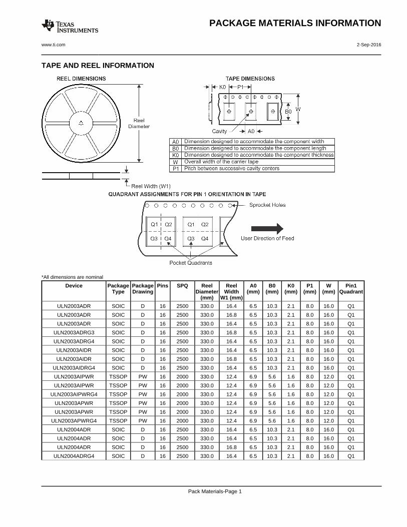
TAPE AND REEL INFORMATION
*All dimensions are nominal
Device PackageType
PackageDrawing
Pins SPQ ReelDiameter
(mm)
ReelWidth
W1 (mm)
A0(mm)
B0(mm)
K0(mm)
P1(mm)
W(mm)
Pin1Quadrant
ULN2003ADR SOIC D 16 2500 330.0 16.4 6.5 10.3 2.1 8.0 16.0 Q1
ULN2003ADR SOIC D 16 2500 330.0 16.8 6.5 10.3 2.1 8.0 16.0 Q1
ULN2003ADR SOIC D 16 2500 330.0 16.4 6.5 10.3 2.1 8.0 16.0 Q1
ULN2003ADRG3 SOIC D 16 2500 330.0 16.8 6.5 10.3 2.1 8.0 16.0 Q1
ULN2003ADRG4 SOIC D 16 2500 330.0 16.4 6.5 10.3 2.1 8.0 16.0 Q1
ULN2003AIDR SOIC D 16 2500 330.0 16.4 6.5 10.3 2.1 8.0 16.0 Q1
ULN2003AIDR SOIC D 16 2500 330.0 16.8 6.5 10.3 2.1 8.0 16.0 Q1
ULN2003AIDRG4 SOIC D 16 2500 330.0 16.4 6.5 10.3 2.1 8.0 16.0 Q1
ULN2003AIPWR TSSOP PW 16 2000 330.0 12.4 6.9 5.6 1.6 8.0 12.0 Q1
ULN2003AIPWR TSSOP PW 16 2000 330.0 12.4 6.9 5.6 1.6 8.0 12.0 Q1
ULN2003AIPWRG4 TSSOP PW 16 2000 330.0 12.4 6.9 5.6 1.6 8.0 12.0 Q1
ULN2003APWR TSSOP PW 16 2000 330.0 12.4 6.9 5.6 1.6 8.0 12.0 Q1
ULN2003APWR TSSOP PW 16 2000 330.0 12.4 6.9 5.6 1.6 8.0 12.0 Q1
ULN2003APWRG4 TSSOP PW 16 2000 330.0 12.4 6.9 5.6 1.6 8.0 12.0 Q1
ULN2004ADR SOIC D 16 2500 330.0 16.4 6.5 10.3 2.1 8.0 16.0 Q1
ULN2004ADR SOIC D 16 2500 330.0 16.4 6.5 10.3 2.1 8.0 16.0 Q1
ULN2004ADR SOIC D 16 2500 330.0 16.8 6.5 10.3 2.1 8.0 16.0 Q1
ULN2004ADRG4 SOIC D 16 2500 330.0 16.4 6.5 10.3 2.1 8.0 16.0 Q1
PACKAGE MATERIALS INFORMATION
www.ti.com 2-Sep-2016
Pack Materials-Page 1
Device PackageType
PackageDrawing
Pins SPQ ReelDiameter
(mm)
ReelWidth
W1 (mm)
A0(mm)
B0(mm)
K0(mm)
P1(mm)
W(mm)
Pin1Quadrant
ULN2004ADRG4 SOIC D 16 2500 330.0 16.4 6.5 10.3 2.1 8.0 16.0 Q1
ULQ2003ADR SOIC D 16 2500 330.0 16.4 6.5 10.3 2.1 8.0 16.0 Q1
ULQ2003ADRG4 SOIC D 16 2500 330.0 16.4 6.5 10.3 2.1 8.0 16.0 Q1
*All dimensions are nominal
Device Package Type Package Drawing Pins SPQ Length (mm) Width (mm) Height (mm)
ULN2003ADR SOIC D 16 2500 333.2 345.9 28.6
ULN2003ADR SOIC D 16 2500 364.0 364.0 27.0
ULN2003ADR SOIC D 16 2500 367.0 367.0 38.0
ULN2003ADRG3 SOIC D 16 2500 364.0 364.0 27.0
ULN2003ADRG4 SOIC D 16 2500 333.2 345.9 28.6
ULN2003AIDR SOIC D 16 2500 333.2 345.9 28.6
ULN2003AIDR SOIC D 16 2500 364.0 364.0 27.0
ULN2003AIDRG4 SOIC D 16 2500 333.2 345.9 28.6
ULN2003AIPWR TSSOP PW 16 2000 364.0 364.0 27.0
ULN2003AIPWR TSSOP PW 16 2000 367.0 367.0 35.0
ULN2003AIPWRG4 TSSOP PW 16 2000 367.0 367.0 35.0
ULN2003APWR TSSOP PW 16 2000 364.0 364.0 27.0
ULN2003APWR TSSOP PW 16 2000 367.0 367.0 35.0
ULN2003APWRG4 TSSOP PW 16 2000 367.0 367.0 35.0
PACKAGE MATERIALS INFORMATION
www.ti.com 2-Sep-2016
Pack Materials-Page 2
Device Package Type Package Drawing Pins SPQ Length (mm) Width (mm) Height (mm)
ULN2004ADR SOIC D 16 2500 367.0 367.0 38.0
ULN2004ADR SOIC D 16 2500 333.2 345.9 28.6
ULN2004ADR SOIC D 16 2500 364.0 364.0 27.0
ULN2004ADRG4 SOIC D 16 2500 367.0 367.0 38.0
ULN2004ADRG4 SOIC D 16 2500 333.2 345.9 28.6
ULQ2003ADR SOIC D 16 2500 333.2 345.9 28.6
ULQ2003ADRG4 SOIC D 16 2500 367.0 367.0 38.0
PACKAGE MATERIALS INFORMATION
www.ti.com 2-Sep-2016
Pack Materials-Page 3
IMPORTANT NOTICE
Texas Instruments Incorporated (TI) reserves the right to make corrections, enhancements, improvements and other changes to itssemiconductor products and services per JESD46, latest issue, and to discontinue any product or service per JESD48, latest issue. Buyersshould obtain the latest relevant information before placing orders and should verify that such information is current and complete.TI’s published terms of sale for semiconductor products (http://www.ti.com/sc/docs/stdterms.htm) apply to the sale of packaged integratedcircuit products that TI has qualified and released to market. Additional terms may apply to the use or sale of other types of TI products andservices.Reproduction of significant portions of TI information in TI data sheets is permissible only if reproduction is without alteration and isaccompanied by all associated warranties, conditions, limitations, and notices. TI is not responsible or liable for such reproduceddocumentation. Information of third parties may be subject to additional restrictions. Resale of TI products or services with statementsdifferent from or beyond the parameters stated by TI for that product or service voids all express and any implied warranties for theassociated TI product or service and is an unfair and deceptive business practice. TI is not responsible or liable for any such statements.Buyers and others who are developing systems that incorporate TI products (collectively, “Designers”) understand and agree that Designersremain responsible for using their independent analysis, evaluation and judgment in designing their applications and that Designers havefull and exclusive responsibility to assure the safety of Designers' applications and compliance of their applications (and of all TI productsused in or for Designers’ applications) with all applicable regulations, laws and other applicable requirements. Designer represents that, withrespect to their applications, Designer has all the necessary expertise to create and implement safeguards that (1) anticipate dangerousconsequences of failures, (2) monitor failures and their consequences, and (3) lessen the likelihood of failures that might cause harm andtake appropriate actions. Designer agrees that prior to using or distributing any applications that include TI products, Designer willthoroughly test such applications and the functionality of such TI products as used in such applications.TI’s provision of technical, application or other design advice, quality characterization, reliability data or other services or information,including, but not limited to, reference designs and materials relating to evaluation modules, (collectively, “TI Resources”) are intended toassist designers who are developing applications that incorporate TI products; by downloading, accessing or using TI Resources in anyway, Designer (individually or, if Designer is acting on behalf of a company, Designer’s company) agrees to use any particular TI Resourcesolely for this purpose and subject to the terms of this Notice.TI’s provision of TI Resources does not expand or otherwise alter TI’s applicable published warranties or warranty disclaimers for TIproducts, and no additional obligations or liabilities arise from TI providing such TI Resources. TI reserves the right to make corrections,enhancements, improvements and other changes to its TI Resources. TI has not conducted any testing other than that specificallydescribed in the published documentation for a particular TI Resource.Designer is authorized to use, copy and modify any individual TI Resource only in connection with the development of applications thatinclude the TI product(s) identified in such TI Resource. NO OTHER LICENSE, EXPRESS OR IMPLIED, BY ESTOPPEL OR OTHERWISETO ANY OTHER TI INTELLECTUAL PROPERTY RIGHT, AND NO LICENSE TO ANY TECHNOLOGY OR INTELLECTUAL PROPERTYRIGHT OF TI OR ANY THIRD PARTY IS GRANTED HEREIN, including but not limited to any patent right, copyright, mask work right, orother intellectual property right relating to any combination, machine, or process in which TI products or services are used. Informationregarding or referencing third-party products or services does not constitute a license to use such products or services, or a warranty orendorsement thereof. Use of TI Resources may require a license from a third party under the patents or other intellectual property of thethird party, or a license from TI under the patents or other intellectual property of TI.TI RESOURCES ARE PROVIDED “AS IS” AND WITH ALL FAULTS. TI DISCLAIMS ALL OTHER WARRANTIES ORREPRESENTATIONS, EXPRESS OR IMPLIED, REGARDING RESOURCES OR USE THEREOF, INCLUDING BUT NOT LIMITED TOACCURACY OR COMPLETENESS, TITLE, ANY EPIDEMIC FAILURE WARRANTY AND ANY IMPLIED WARRANTIES OFMERCHANTABILITY, FITNESS FOR A PARTICULAR PURPOSE, AND NON-INFRINGEMENT OF ANY THIRD PARTY INTELLECTUALPROPERTY RIGHTS. TI SHALL NOT BE LIABLE FOR AND SHALL NOT DEFEND OR INDEMNIFY DESIGNER AGAINST ANY CLAIM,INCLUDING BUT NOT LIMITED TO ANY INFRINGEMENT CLAIM THAT RELATES TO OR IS BASED ON ANY COMBINATION OFPRODUCTS EVEN IF DESCRIBED IN TI RESOURCES OR OTHERWISE. IN NO EVENT SHALL TI BE LIABLE FOR ANY ACTUAL,DIRECT, SPECIAL, COLLATERAL, INDIRECT, PUNITIVE, INCIDENTAL, CONSEQUENTIAL OR EXEMPLARY DAMAGES INCONNECTION WITH OR ARISING OUT OF TI RESOURCES OR USE THEREOF, AND REGARDLESS OF WHETHER TI HAS BEENADVISED OF THE POSSIBILITY OF SUCH DAMAGES.Unless TI has explicitly designated an individual product as meeting the requirements of a particular industry standard (e.g., ISO/TS 16949and ISO 26262), TI is not responsible for any failure to meet such industry standard requirements.Where TI specifically promotes products as facilitating functional safety or as compliant with industry functional safety standards, suchproducts are intended to help enable customers to design and create their own applications that meet applicable functional safety standardsand requirements. Using products in an application does not by itself establish any safety features in the application. Designers mustensure compliance with safety-related requirements and standards applicable to their applications. Designer may not use any TI products inlife-critical medical equipment unless authorized officers of the parties have executed a special contract specifically governing such use.Life-critical medical equipment is medical equipment where failure of such equipment would cause serious bodily injury or death (e.g., lifesupport, pacemakers, defibrillators, heart pumps, neurostimulators, and implantables). Such equipment includes, without limitation, allmedical devices identified by the U.S. Food and Drug Administration as Class III devices and equivalent classifications outside the U.S.TI may expressly designate certain products as completing a particular qualification (e.g., Q100, Military Grade, or Enhanced Product).Designers agree that it has the necessary expertise to select the product with the appropriate qualification designation for their applicationsand that proper product selection is at Designers’ own risk. Designers are solely responsible for compliance with all legal and regulatoryrequirements in connection with such selection.Designer will fully indemnify TI and its representatives against any damages, costs, losses, and/or liabilities arising out of Designer’s non-compliance with the terms and provisions of this Notice.
Mailing Address: Texas Instruments, Post Office Box 655303, Dallas, Texas 75265Copyright © 2017, Texas Instruments Incorporated