Embed Size (px)
Citation preview
“Ultra-Low Jitter Oscillators”ASG-ULJ Series

Ideal for High Data Rate Applications
2
Test & Measurement
- Spectrum analyzers - Oscilloscopes- ATE
High Speed Networking
- 10/40/100/400 Gigabit Ethernet- High port count switches
Medical Imaging
- High resolution endoscopy- MRI
Server
- High speed interconnect- FPGA accelerator add-on cards
Wireless Infrastructure
- High speed back haul- Base stations (BTS)- RF Data converters
Storage
- Storage Area Networks- 32Gbps Fibre Channel- Network Attached Storage

0.1ps
1.0ps
10.0ps
100.0ps
1Gbps 10Gbps 100Gbps
RM
S P
has
e JI
tter
(12
kHz
to 2
0M
Hz
inte
grat
ion
ran
ge)
Serial Data Rate
Maximum Recommended Clock RMS Phase Jitter vs Serial Data Rate
3
Challenge: Maintain low BER while bit rates double or quadruple
56Gbps requiring 0.2ps RMS max(12k to 20MHz)
‒ Higher data rates demand lower clock jitter to maintain low bit error rate (BER)
‒ Excessive or undeterminable clock jitter induces failures and usually increases design and debug time
4
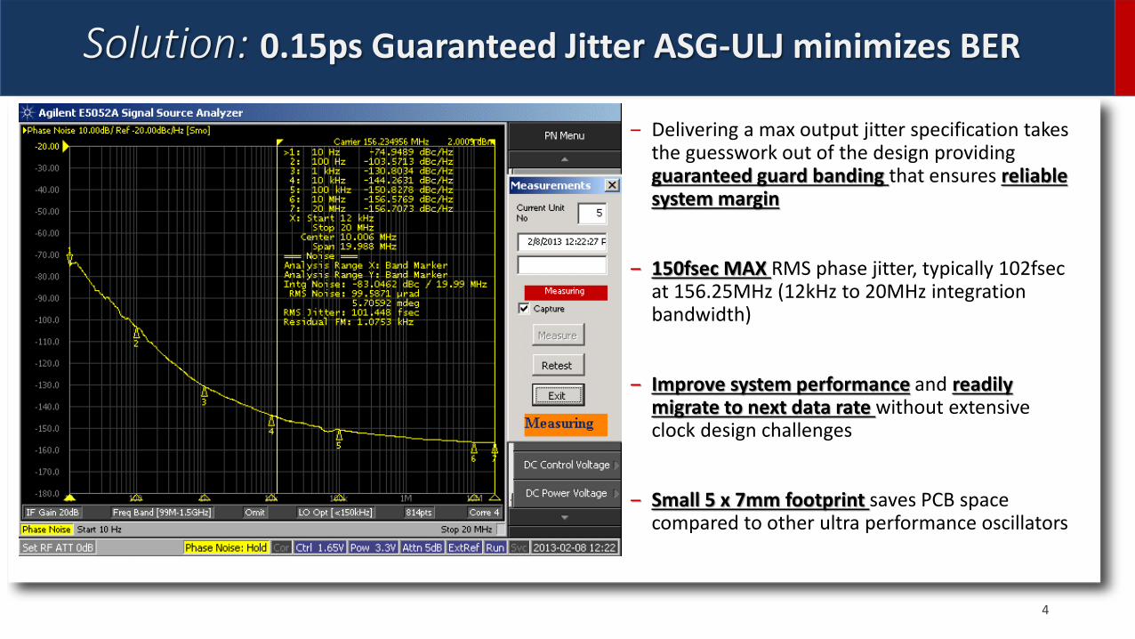
Solution: 0.15ps Guaranteed Jitter ASG-ULJ minimizes BER
‒ Delivering a max output jitter specification takes the guesswork out of the design providing guaranteed guard banding that ensures reliable system margin
‒ 150fsec MAX RMS phase jitter, typically 102fsec at 156.25MHz (12kHz to 20MHz integration bandwidth)
‒ Improve system performance and readily migrate to next data rate without extensive clock design challenges
‒ Small 5 x 7mm footprint saves PCB space compared to other ultra performance oscillators
5
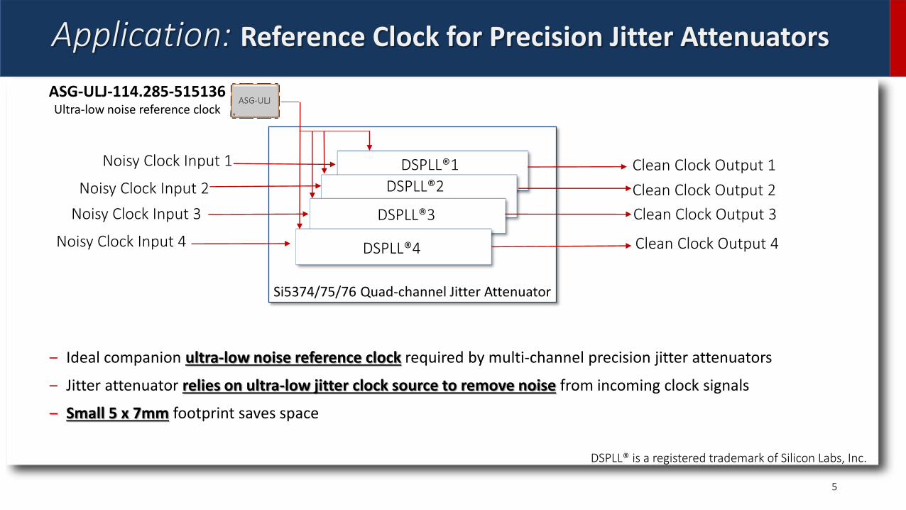
Application: Reference Clock for Precision Jitter Attenuators
Noisy Clock Input 1 DSPLL®1
DSPLL®2
DSPLL®3
DSPLL®4
Noisy Clock Input 2
Noisy Clock Input 3
Noisy Clock Input 4
Si5374/75/76 Quad-channel Jitter Attenuator
Clean Clock Output 1
Clean Clock Output 2
Clean Clock Output 3
Clean Clock Output 4
‒ Ideal companion ultra-low noise reference clock required by multi-channel precision jitter attenuators
‒ Jitter attenuator relies on ultra-low jitter clock source to remove noise from incoming clock signals
‒ Small 5 x 7mm footprint saves space
ASG-ULJ-114.285-515136Ultra-low noise reference clock
DSPLL® is a registered trademark of Silicon Labs, Inc.
6
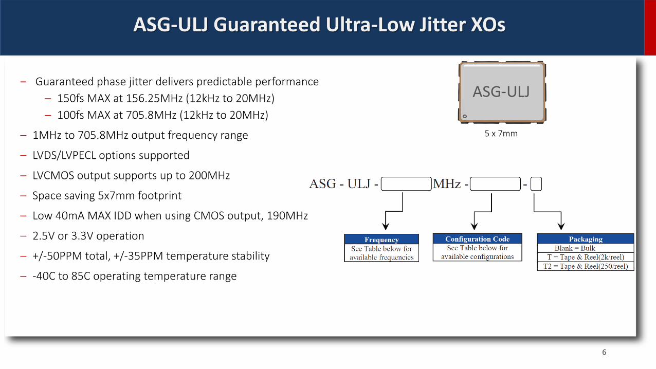
ASG-ULJ Guaranteed Ultra-Low Jitter XOs
‒ Guaranteed phase jitter delivers predictable performance
‒ 150fs MAX at 156.25MHz (12kHz to 20MHz)
‒ 100fs MAX at 705.8MHz (12kHz to 20MHz)
‒ 1MHz to 705.8MHz output frequency range
‒ LVDS/LVPECL options supported
‒ LVCMOS output supports up to 200MHz
‒ Space saving 5x7mm footprint
‒ Low 40mA MAX IDD when using CMOS output, 190MHz
‒ 2.5V or 3.3V operation
‒ +/-50PPM total, +/-35PPM temperature stability
‒ -40C to 85C operating temperature range
5 x 7mm
7
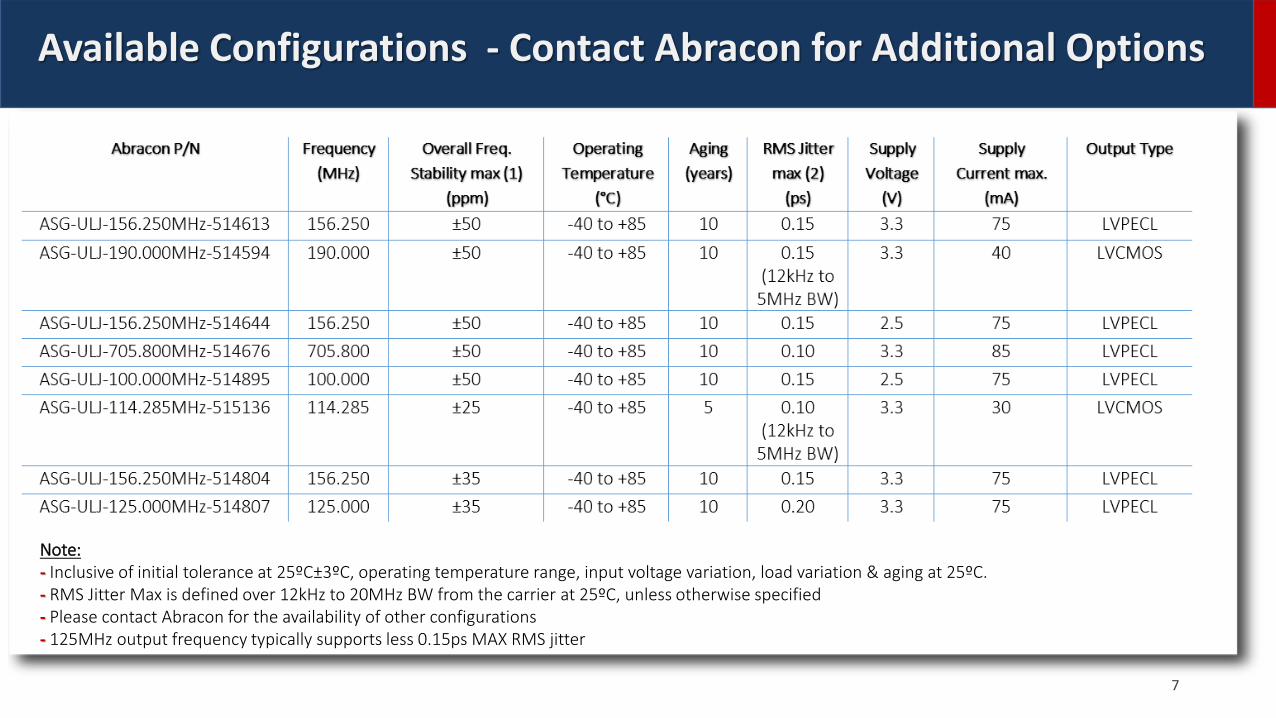
Available Configurations - Contact Abracon for Additional Options
Note: - Inclusive of initial tolerance at 25ºC±3ºC, operating temperature range, input voltage variation, load variation & aging at 25ºC.- RMS Jitter Max is defined over 12kHz to 20MHz BW from the carrier at 25ºC, unless otherwise specified- Please contact Abracon for the availability of other configurations- 125MHz output frequency typically supports less 0.15ps MAX RMS jitter

8
XO- Ultra-Low Jitter for High Bandwidth Applications
-RF and basestations
Carrier frequency 100MHz52fs

9
THANK YOU!