Embed Size (px)
Citation preview

1. General description
The QN9080-001-M17 is a fully certified device supporting BLE and NFC. It has ultra-low power consumption, highly integrated with rich feature sets, fully FCC/CE/IC/MIC certified. The QN9080-001-M17 supports Bluetooth 5, and it is intended for ultra-small, portable connected wireless applications.
This ultra-small device is based on QN9080 die and NT3H2211 die. QN9080 is powered by an Arm Cortex-M4F, and has a dedicated fusion sensor co-processor (FSP) to further reduce power consumption by off-loading complex math computations to the hardware. 512 KB of on-board flash and 128 KB SRAM provide enough room and flexibility for complex applications. NT3H2211 is NFC Forum Type 2 Tag compliant IC with I2C interface, which supplies the fastest, least expensive way to add tap-and-go connectivity to just about any electronic applications.
The QN9080-001-M17 also integrates 32 MHz and 32.768 kHz crystals, a 2.4 GHz optimized antenna, and necessary components for QN9080 system to run. It offers a complete solution for applications requiring BLE wireless connectivity and fast pairing with NTAG as an option. Its low external component count reduces overall system size, complexity and shortens development time.
2. Features and benefits
Key features: Bluetooth 5.0 certified Integrated antenna Integrated 32 MHz and 32.768 kHz crystals 32-bit Arm Cortex-M4F core at 32 MHz 512 KB flash 128 KB RAM TX power: up to +2 dBm RX sensitivity: -92.7 dBm in 1 Mbps mode and -89 dBm in 2 Mbps mode
True single-chip Bluetooth Low Energy (v5.0) SoC solution: Integrated Bluetooth LE radio, protocol stack and application profiles Support central and peripherals roles Support master/slave concurrency Support 16 simultaneous links Support secure connections Support data packet length extension 48-bit unique BD address -92.7 dBm in 1 Mbps mode and -89 dBm in 2 Mbps mode
QN9080-001-M17Ultra Low-Power Bluetooth Smart 5.0 SIPRev. 1.0 — 5 December 2018 Objective data sheet

NXP Semiconductors Ultra Low-Power Bluetooth SmartQN9080-001-M17
TX output power from -20 dBm to +2 dBm Very low power consumption: Single 1.67 V ~3.6 V power supply 1 A power-down mode, to wake up by GPIO 2 A power-down mode, to wake up by 32 kHz sleep timer, RTC and GPIO 4 mA RX current at 3 V supply in 1 Mbps Ultra Low power Bluetooth Low Energy 5.0 module 3.5 mA TX current at 0 dBm TX power at 3 V supply in 1 Mbps mode
Interface: 32 General-Purpose Input/Output (GPIO) pins, with configurable pull-up/pull-down
resistors 8 external ADC inputs (shared with GPIO pins) 2 Analog Comparator input pins (share with GPIO pins)
Single power supply 1.67 V to 3.6 V Operating temperature range -40 °C to +85 °C 6 x9.7x1.17 mm LFLGA package
2.1 Feature of QN9080 True single-chip Bluetooth Low Energy (v5.0) SoC solution Integrated Bluetooth LE radio, protocol stack and application profiles Supports central and peripherals roles Supports master/slave concurrency Supports 16 simultaneous links Supports secure connections Supports data packet length extensionWifi/Bluetooth LE coexistence interface 48-bit unique bluetooth device address
RF Fast and reliable RSSI in 1 dB step TX output power from 20 dBm to 2 dBm Single-ended RF port with integrated balun Generic FSK modulation with programmed data rate from 250 Kbps to 2 Mbps Compatible with worldwide radio frequency regulations
Very low power consumption Single 1.67 V to 3.6 V power supply Integrated DC-to-DC buck converter and LDO 1.0 A power-down 1 mode, to wake up by GPIO 2.5 A power-down 0 mode, to wake up by 32 kHz sleep timer, RTC and GPIO 3.5 mA RX current with DC-to-DC convertor enabled at 3 V supply in 1Mbps mode 4 mA TX current at 0 dBm TX power with DC-to-DC converter enabled at 3 V
supply in 1 Mbps mode Arm Cortex-M4 core (version r0p1) Arm Cortex-M4 processor, running at a frequency of up to 32 MHz Floating Point Unit (FPU) and Memory Protection Unit (MPU)
QN9080-001-M17 All information provided in this document is subject to legal disclaimers. © NXP Semiconductors B.V. 2018. All rights reserved.
Objective data sheet Rev. 1.0 — 5 December 2018 2 of 39

NXP Semiconductors Ultra Low-Power Bluetooth SmartQN9080-001-M17
Arm Cortex-M4 built-in Nested Vectored Interrupt Controller (NVIC) Serial Wire Debug (SWD) with six instruction breakpoints, two literal comparators,
and four watch points, including serial wire output for enhanced debug capabilities System tick timer
On-chip memory 512 KB on-chip flash program memory and 2 KB page erase and write 128 KB SRAM 256 KB ROM
ROM API support Flash In-System Programming (ISP)
Serial interfaces Four Flexcomm serial peripherals USART protocol supported by Flexcomm0, USART and I2C by Flexcomm1, SPI
and I2C by Flexcomm2, and SPI by Flexcomm3 Each Flexcomm includes a FIFO I2C-bus interfaces support fast mode and with multiple address recognition and
monitor mode USB 2.0 (full speed) device interface Two quadrature decoders SPI Flash Interface (SPIFI) uses a SPI bus superset with four data lines to access
off-chip quad SPI flash memory at a much higher rate than is possible using standard SPI or SSP interfaces
Supports SPI memories with 1 or 4 data lines Digital peripherals DMA controller with 20 channels, able to access memories and DMA capable
peripherals Up to 35 General Purpose Input Output (GPIO) pins, with configurable pull-up or
pull-down resistors GPIO registers are located on the AHB for fast access 32 GPIOs can be selected as Pin INTerrupts (PINT), triggered by rising, or falling
input edges AES-128 security coprocessor Random Number Generator (RNG) CRC engine Fusion Signal Processor (FSP) for data fusion and machine learning algorithms
resulting in low power consumption compared to software processing
QN9080-001-M17 All information provided in this document is subject to legal disclaimers. © NXP Semiconductors B.V. 2018. All rights reserved.
Objective data sheet Rev. 1.0 — 5 December 2018 3 of 39

NXP Semiconductors Ultra Low-Power Bluetooth SmartQN9080-001-M17
Analog peripherals 16-bit ADC with 8 external input channels, with sample rates of up to 32k sample
per second, and with multiple internal and external trigger inputs Integrated temperature sensor, connected to one internal dedicated ADC channel Integrated battery monitor connected to one internal dedicated ADC channel General-purpose 8-bit 1M sample per second DAC Integrated capacitive sense up to 8 channels, able to wake up the MCU from low
power states. Two ultra low-power analog comparators, able to wake up the MCU from low power
states. Timers Four 32-bit general-purpose timers or counters, support capture inputs and
compare outputs, PWM mode, and external count input Sleep timer, which can work in power-down mode and wake up MCU 32-bit Real Time Clock (RTC) with 1 second resolution running in the always-on
power domain; can be used for wake-up from all low power modes including power-down
Watchdog Timer. SC Timer or PWM.
Clock generation 32 MHz internal RC oscillator, which can be used as a system clock 16 MHz or 32 MHz crystal oscillator, which can be used as a system and RF
reference 32 kHz on-chip RC oscillator 32.768 kHz crystal oscillator
Power control Programmable Power Management Unit (PMU) to minimize power consumption Reduced power modes: sleep, and power-down Power-On Reset (POR) Brown-Out Detection (BOD) with separate thresholds for interrupt and forced reset
Single power supply 1.67 V to 3.6 V Operating temperature range 40 °C to +85 °C
See QN908x data sheet for more details.
2.2 Features of NTAG Interoperability ISO/IEC 14443 Part 2 and 3 compliant NTAG I2C plus development board is certified as NFC Forum Type 2 Tag
(Certification ID: 58514) Unique 7-byte UID GET_VERSION command for easy identification of chip type and supported
features Input capacitance of 50 pF
Host interface I2C slave
QN9080-001-M17 All information provided in this document is subject to legal disclaimers. © NXP Semiconductors B.V. 2018. All rights reserved.
Objective data sheet Rev. 1.0 — 5 December 2018 4 of 39

NXP Semiconductors Ultra Low-Power Bluetooth SmartQN9080-001-M17
Configurable event detection pin to signal NFC or pass-through data events Memory 1912 bytes of EEPROM-based user memory 64 bytes SRAM buffer for transfer of data between NFC and I2C interfaces with
memory mirror or pass-through mode Clear arbitration between NFC and I2C memory access
Data transfer Pass-through mode with 64-byte SRAM buffer FAST_WRITE and FAST_READ NFC commands for higher data throughput
Security and memory-access management Full, read-only, or no memory access from NFC interface, based on 32-bit
password Full, read-only, or no memory access from I2C interface NFC silence feature to disable the NFC interface Originality signature based on Elliptic Curve Cryptography (ECC) for simple,
genuine authentication Power Management Configurable field-detection output signal for data-transfer synchronization and
device wake-up Energy harvesting from NFC field, so as to power external devices (e.g. connected
microcontroller)
See NT3H2111_2211 Product Data Sheet for more details.
2.3 Features of integrated 2.4 GHz antenna Monolithic SMD with small, low-profile and light-weight type. Wide bandwidth RoHS compliant
Note: When NFC function is required, the NFC tag antenna need to be connected externally.
3. Applications
Health and medical devices Sports and fitness trackers Building and home automation Retail and advertising beacons
4. Ordering information
Table 1. Ordering information Type number Package
Name Description VersionQN9080-001-M17 LFLGA54 SIP module in LGA package; body 6 9.7 1.17 mm SOT1910 AA1
QN9080-001-M17 All information provided in this document is subject to legal disclaimers. © NXP Semiconductors B.V. 2018. All rights reserved.
Objective data sheet Rev. 1.0 — 5 December 2018 5 of 39

NXP Semiconductors Ultra Low-Power Bluetooth SmartQN9080-001-M17
5. Marking
QN9080-001-M17 has the following top-side marking:
QN9080-001-M17 device has received FCC "Modular Approval", in compliance with CFR 47 FCC part 15 regulations and in accordance to FCC public notice DA00-1407. The modular approvals notice and test reports are available on request.
Remark: FCC, IC & Japan ID are not mentioned on the package due to the small device size.
Table 2. Ordering options Type number Package
numberFlash (KB) Total SRAM
(KB)Cortex-M4 with FPU
FSP USB FS GPIO
QN9080-001-M17 3322 960 18570 512 128 1 1 1 32
Fig 1. QN9080-001-M17 package marking
Table 3. Marking codes Line
numberContent Descriptions
1 NXP Logo2 QN9080-1-M17 Product identifier3 XXXXX STR number request. It will be removed on production4 XXXXXXXXXXXX QN batch number5 E TSMC
t ASE-KD RoHS indicator (Dark green)YY year; last two digits of year code of assemblyWW week code of assemblyX mask versionX for SIP before CQS; it will be removed after
Table 4. Device revision tableRevision identifier (R) Revision description
001 Initial SIP module revision
QN9080-1-M17
EtDYYWWXX
XXXXXXXXXXXXXXXXX
QN9080-001-M17 All information provided in this document is subject to legal disclaimers. © NXP Semiconductors B.V. 2018. All rights reserved.
Objective data sheet Rev. 1.0 — 5 December 2018 6 of 39

NXP Semiconductors Ultra Low-Power Bluetooth SmartQN9080-001-M17
6. Block diagram
Fig 2. QN9080-001-M17 – high level HW block diagram
Antenna
CHRG_SCL
CHRG_SDA
VCC
IDC
DVDD RVDD AVDD
VCC
PA31-PA00
CHIP_MODE
RSTN
GNDVSS
DAPGND
ANT IN
RF OUT
NTAG_LA
NTAG_LB
NTAG_VOUT
GND
NTAG_FD NTAG_VCC
SCL
SDA
RF
XTAL_OUT
XTAL_IN
Harmonic filter
C21.8 pF
L2 3.3 nH
C11.8 pF
Y132 MHz
C40.1 F
C30.1 F
C50.1 F
L3 10nH
L110 H
XTAL32_IN
XTAL32_OUT
Y232.768 kHz
C61 F
FD
NTAGNT3H2211
QN9080 die
QN9080M
DCDC
QN9080-001-M17 All information provided in this document is subject to legal disclaimers. © NXP Semiconductors B.V. 2018. All rights reserved.
Objective data sheet Rev. 1.0 — 5 December 2018 7 of 39

NXP Semiconductors Ultra Low-Power Bluetooth SmartQN9080-001-M17
Remark: (1) QN9080-001-M17 is not certified with external antenna but only with its internal antenna. Customer using external antenna has to do new certification. (2) Harmonic filter is in adequacy with board.
Fig 3. QN9080-001-M17 block diagram using external antenna
Antenna
CHRG_SCL
CHRG_SDA
VCC
IDC
DVDD RVDD AVDD
VCC
PA31-PA00
CHIP_MODE
RSTN
GNDVSS
DAPGND
ANT IN
RF OUT
NTAG_LA
NTAG_LB
NTAG_VOUT
GND
NTAG_FD NTAG_VCC
SCL
SDA
RF
XTAL_OUT
XTAL_IN
Harmonic filter
C21.8 pF
L2 3.3 nH
C11.8 pF
Y132 MHz
C40.1 F
C30.1 F
C50.1 F
L3 10nH
L110 H
XTAL32_IN
XTAL32_OUT
Y232.768 kHz
C61 F
FD
NTAGNT3H2211
QN9080 die
QN9080M
DCDC
ExternalAntenna
Harmonic filter
C11.8 pF
L2 3.3 nH
C21.8 pF
Designed and provided by customer
QN9080-001-M17 All information provided in this document is subject to legal disclaimers. © NXP Semiconductors B.V. 2018. All rights reserved.
Objective data sheet Rev. 1.0 — 5 December 2018 8 of 39
NXP Semiconductors Ultra Low-Power Bluetooth SmartQN9080-001-M17
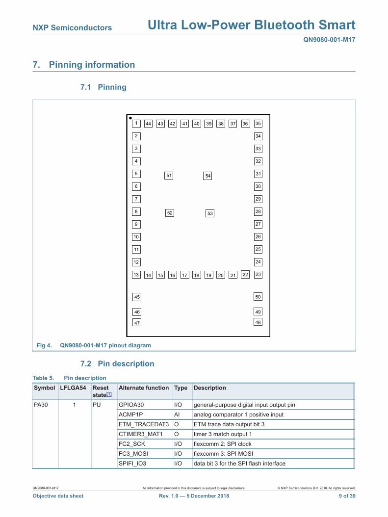
7. Pinning information
7.1 Pinning
7.2 Pin description
Fig 4. QN9080-001-M17 pinout diagram
1
2
3
4
5
6
7
8
9
10
11
12
13 14 15 16 17 18 19 20 21 22 23
24
25
26
27
28
29
30
31
32
33
34
35363738394041424344
45
46
47 48
49
50
51
52 53
54
Table 5. Pin description Symbol LFLGA54 Reset
state[1]Alternate function Type Description
PA30 1 PU GPIOA30 I/O general-purpose digital input output pinACMP1P AI analog comparator 1 positive inputETM_TRACEDAT3 O ETM trace data output bit 3CTIMER3_MAT1 O timer 3 match output 1FC2_SCK I/O flexcomm 2: SPI clockFC3_MOSI I/O flexcomm 3: SPI MOSISPIFI_IO3 I/O data bit 3 for the SPI flash interface
QN9080-001-M17 All information provided in this document is subject to legal disclaimers. © NXP Semiconductors B.V. 2018. All rights reserved.
Objective data sheet Rev. 1.0 — 5 December 2018 9 of 39

NXP Semiconductors Ultra Low-Power Bluetooth SmartQN9080-001-M17
PA29 2 PU GPIOA29 I/O general-purpose digital input output pinACMP1N AI analog comparator 1 negative inputETM_TRACEDAT2 O ETM trace data output bit 2CTIMER3_MAT0 O timer 3 match output 0FC2_SCK I/O flexcomm 2: SPI clockFC3_MISO I/O flexcomm 3: SPI MISOSPIFI_IO2 I/O data bit 2 for the SPI flash interface
PA28 3 PU GPIOA28 I/O general-purpose digital input output pinCLK_AHB O AHB clock outputETM_TRACECLK O ETM trace clock outputRTC_CAP I RTC capture inputFC1_SCK I/O flexcomm 1: USART clockSD_DAC O sigma-delta modulator DAC outputSPIFI_CSN O active low chip select output for the SPI flash interface
PA27 4 PU GPIOA27 I/O general-purpose digital input output pinUSB_DM I/O USB0 bidirectional D- lineSCT0_IN1 I SCTimer input 1CTIMER1_MAT2 O 32-bit CTimer 1 match output 2FC2_SCL_MISO I/O flexcomm 2: I2C SCL, SPI MISOQDEC0_B I quadrature decoder 0 input channel BBLE_IN_PROC O BLE event in process indicator for coexistence
PA26 5 PU GPIOA26 I/O general-purpose digital input output pinUSB_DP I/O USB0 bidirectional D+ lineSCT0_IN0 I SCTimer input 0CTIMER1_MAT0 O 32-bit CTimer 1 match output 0FC2_SDA_MOSI I/O flexcomm 2: I2C SDA, SPI MOSIQDEC0_A I quadrature decoder 0 input channel ABLE_SYNC O BLE sync pulse
LB 6 RF NTAG antenna/coil terminal BLA 7 RF NTAG antenna/coil terminal APA25 8 PU GPIOA25 I/O general-purpose digital input output pin
ACMP0P/CS7 AI analog comparator 0 positive input, or capacitive touch sense button input 7
ETM_TRACEDAT1 O ETM trace data output bit 1CTIMER3_CAP1 I timer 3 input capture 1RFE_TX_EN O TX enable for external RF front-endFC3_SSEL0 I/O flexcomm 3: SPI SSEL0SPIFI_IO1 I/O data bit 1 for the SPI flash interface
Table 5. Pin description …continued
Symbol LFLGA54 Reset state[1]
Alternate function Type Description
QN9080-001-M17 All information provided in this document is subject to legal disclaimers. © NXP Semiconductors B.V. 2018. All rights reserved.
Objective data sheet Rev. 1.0 — 5 December 2018 10 of 39

NXP Semiconductors Ultra Low-Power Bluetooth SmartQN9080-001-M17
PA24 9 PU GPIOA24 I/O general-purpose digital input output pinACMP0N/CS6 AI analog comparator 0 negative input, or capacitive touch
sense button input 6ETM_TRACEDAT0 O ETM trace data output bit 0CTIMER3_CAP0 I timer 3 input capture 0RFE_RX_EN O RX enable for external RF front-endFC3_SSEL1 I/O flexcomm 3: SPI SSEL1SPIFI_IO0 I/O data bit 0 for the SPI flash interface
SWDIO/PA23
10 PU SWDIO I/O serial wire debug I/O; it is the default function after bootingGPIOA23 I/O general-purpose digital input output pinSCT0_IN3 I SCTimer input 3CTIMER3_MAT1 O 32-bit CTimer 3 match output 1FC2_SCL_SSEL1 I/O flexcomm 2: I2C SCL, SPI SSEL1FC3_SSEL2 I/O flexcomm 3: SPI SSEL2QDEC1_B I quadrature decoder 1 input channel B
SWCLK/PA22
11 PU SWCLK I/O serial wire clock; it is the default function after resetGPIOA22 I/O general-purpose digital input output pinSCT0_IN2 I SCTimer input 2CTIMER3_MAT0 O 32-bit CTimer 3 match output 0FC2_SDA_SSEL0 I/O flexcomm 2: I2C SDA, SPI SSEL0FC3_SSEL3 I/O flexcomm 3: SPI SSEL3QDEC1_A I quadrature decoder 1 input channel A
PA21 12 PU GPIOA21 I/O general-purpose digital input output pinQDEC1_B I quadrature decoder 1 input channel BSCT0_OUT0 O SCTimer output 0, PWM output 0CTIMER2_MAT1 O 32-bit CTimer 2 match output 1FC2_SSEL3 I/O flexcomm 2: SPI SSEL3FC1_CTS_SDA I/O flexcomm 1: USART CTS, I2C SDASPIFI_CSN O active low chip select output for the SPI flash interface
PA20 13 PU GPIOA20 I/O general-purpose digital input output pinQDEC1_A I quadrature decoder 1 input channel ASCT0_OUT1 O SCTimer output 1, PWM output 1CTIMER2_MAT0 O 32-bit CTimer 2 match output 0SWO I/O serial wire trace outputFC1_RTS_SCL I/O flexcomm 1: USART RTS, I2C SCLSPIFI_CLK O clock output for the SPI flash interface
Table 5. Pin description …continued
Symbol LFLGA54 Reset state[1]
Alternate function Type Description
QN9080-001-M17 All information provided in this document is subject to legal disclaimers. © NXP Semiconductors B.V. 2018. All rights reserved.
Objective data sheet Rev. 1.0 — 5 December 2018 11 of 39

NXP Semiconductors Ultra Low-Power Bluetooth SmartQN9080-001-M17
PA19 14 PU GPIOA19 I/O general-purpose digital input output pinCS5 AI capacitive touch sense button input 5SCT0_OUT2 O SCTimer output 2, PWM output 2RFE_EN O enable for external RF front-endFC0_SCK I/O flexcomm 0: USART clockFC3_SSEL3 I/O flexcomm 3: SPI SSEL3BLE_IN_PROC O BLE event in process indicator for coexistence
PA18 15 PU GPIOA18 I/O general-purpose digital input output pinCS4 AI capacitive touch sense button input 4SCT0_OUT3 O SCTimer output 3, PWM output 3CTIMER2_MAT2 O 32-bit CTimer 2 match output 2FC0_SCK I/O flexcomm 0: USART clockFC3_SSEL2 I/O flexcomm 3: SPI SSEL2BLE_SYNC O BLE sync pulse
PA17 16 PU GPIOA17 I/O general-purpose digital input output pinCS3 AI capacitive touch sense button input 3SD_DAC O sigma-delta modulator DAC outputCTIMER2_MAT1 O 32-bit CTimer 2 match output 1FC0_RXD I/O flexcomm 0: USART RXDFC3_MISO I/O flexcomm 3: SPI MISOQDEC0_B I quadrature decoder 0 input channel B
PA16 17 PU GPIOA16 I/O general-purpose digital input output pinCS2 AI capacitive touch sense button input 2SCT0_OUT1 O SCTimer output 1, PWM output 1CTIMER2_MAT0 O 32-bit CTimer 2 match output 0FC0_TXD I/O flexcomm 0: USART TXDFC3_MOSI I/O flexcomm 3: SPI MOSIQDEC0_A I quadrature decoder 0 input channel A
PA15 18 PU GPIOA15 I/O general-purpose digital input output pinCS1 AI capacitive touch sense button input 1SCT0_OUT0 O SCTimer output 0, PWM output 0CTIMER2_CAP1 I timer 2 input capture 1FC0_CTS I/O flexcomm 0: USART CTSFC3_SCK I/O flexcomm 3: SPI clockQDEC1_B I quadrature decoder 1 input channel B
Table 5. Pin description …continued
Symbol LFLGA54 Reset state[1]
Alternate function Type Description
QN9080-001-M17 All information provided in this document is subject to legal disclaimers. © NXP Semiconductors B.V. 2018. All rights reserved.
Objective data sheet Rev. 1.0 — 5 December 2018 12 of 39

NXP Semiconductors Ultra Low-Power Bluetooth SmartQN9080-001-M17
PA14 19 PU GPIOA14 I/O general-purpose digital input output pinCS0 AI capacitive touch sense button input 0ANT_SW O external antenna switch for diversityCTIMER2_CAP0 I timer 2 input capture 0FC0_RTS I/O flexcomm 0: USART RTSFC3_SSEL0 I/O flexcomm 3: SPI SSEL0QDEC1_A I quadrature decoder 1 input channel A
PA13 20 PU GPIOA13 I/O general-purpose digital input output pinR I/O reservedSCT0_OUT4 O SCTimer output 4ACMP1_OUT O analog comparator 1 outputFC1_RXD_SDA I/O flexcomm 1: USART RXD, I2C SDAFC3_SSEL1 I/O flexcomm 3: SPI SSEL1RFE_EN O enable for external RF front-end
CHIP_MODE/PB02
21 PU CHIP_MODE I boot selection with pull-up by default; it should be pulled low to go through the normal ISP process for firmware programming, otherwise the ISP process is escaped to jump to flash
GPIOB02 I/O general-purpose digital input output pinANT_SW O external antenna switch for diversity
RSTN 22 PU I active low reset inputANT_IN 23 RF Internal antennaRF_OUT
24 RF RF input output port with Tx or Rx switch integrated on chip
GND 25 groundPA12 26 PU GPIOA12 I/O general-purpose digital input output pin
R O reservedSCT0_OUT5 O SCTimer output 5ACMP0_OUT O analog comparator 0 outputFC1_TXD_SCL I/O flexcomm 1: USART TXD, I2C SCLSD_DAC O sigma-delta modulator DAC outputANT_SW O external antenna switch for diversity
PA11 27 PU GPIOA11 I/O general-purpose digital input output pinADC7 AI ADC external input 7SCT0_IN3 I SCTimer input 3CTIMER1_MAT2 O 32-bit CTimer 1 match output 2FC2_SSEL2 I/O flexcomm 2: SPI SSEL2ACMP1_OUT O analog comparator 1 outputBLE_RX O BLE reception indicator for coexistence
Table 5. Pin description …continued
Symbol LFLGA54 Reset state[1]
Alternate function Type Description
QN9080-001-M17 All information provided in this document is subject to legal disclaimers. © NXP Semiconductors B.V. 2018. All rights reserved.
Objective data sheet Rev. 1.0 — 5 December 2018 13 of 39

NXP Semiconductors Ultra Low-Power Bluetooth SmartQN9080-001-M17
PA10 28 PU GPIOA10 I/O general-purpose digital input output pinADC6 AI ADC external input 6SCT0_IN2 I SCTimer input 2CTIMER1_MAT1 O 32-bit CTimer 1 match output 1FC1_SCK I/O flexcomm 1: USART clockACMP0_OUT O analog comparator 0 outputBLE_TX O BLE transmit indicator for coexistence
PA09 29 PU GPIOA9 I/O general-purpose digital input output pinADC5 AI ADC external input 5SCT0_IN1 I SCTimer input 1CTIMER1_MAT0 O 32-bit CTimer 1 match output 0FC1_RXD_SDA I/O flexcomm 1: USART RXD, I2C SDABLE_PTI3 O BLE packet traffic information bit 3SPIFI_IO3 I/O data bit 3 for the SPI flash interface
PA08 30 PU GPIOA8 I/O general-purpose digital input output pinADC4 AI ADC external input 4SCT0_IN0 I SCTimer input 0CTIMER1_CAP1 I timer 1 input capture 1FC1_TXD_SCL I/O flexcomm 1: USART TXD, I2C SCLBLE_PTI2 O BLE packet traffic information 2SPIFI_IO2 I/O data bit 2 for the SPI flash interface
PA07 31 PU GPIOA7 I/O general-purpose digital input output pinADC_VREFI AI ADC external reference voltage inputSCT0_OUT2 O SCTimer output 2CTIMER1_CAP0 I timer 1 input capture 0FC1_CTS_SDA I/O flexcomm 1: USART CTS, I2C SDABLE_PTI1 O BLE packet traffic information 1SPIFI_CSN O active low chip select output for the SPI flash interface
PA06 32 PU GPIOA6 I/O general-purpose digital input output pinADC_EX_CAP A connected with ADC external capacitor SCT0_OUT3 O SCTimer output 3CTIMER0_MAT2 O 32-bit CTimer 0 match output 2FC1_RTS_SCL I/O flexcomm 1: USART RTS, I2C SCLBLE_PTI0 O BLE packet traffic information bit 0SPIFI_CLK O clock output for the SPI flash interface
Table 5. Pin description …continued
Symbol LFLGA54 Reset state[1]
Alternate function Type Description
QN9080-001-M17 All information provided in this document is subject to legal disclaimers. © NXP Semiconductors B.V. 2018. All rights reserved.
Objective data sheet Rev. 1.0 — 5 December 2018 14 of 39

NXP Semiconductors Ultra Low-Power Bluetooth SmartQN9080-001-M17
PA05 33 PU GPIOA5 I/O general-purpose digital input output pinADC3 AI ADC external input 3SCT0_OUT5 O SCTimer output 5CTIMER0_MAT1 O 32-bit CTimer 0 match output 1FC0_RXD I/O flexcomm 0: USART RXDFC2_SCL_MISO I/O flexcomm 2: SCL, SPI MISOSPIF_IO1 I/O data bit 1 for the SPI flash interface
PA04 34 PU GPIOA4 I/O general-purpose digital input output pinADC2 AI ADC external input 2SCT0_OUT4 O SCTimer output 4CTIMER0_MAT0 O 32-bit CTimer 0 match output 0FC0_TXD I/O flexcomm 0: USART TXDFC2_SDA_MOSI I/O flexcomm 2: I2C SDA, SPI MOSISPIF_IO0 I/O data bit 0 for the SPI flash interface
PA03 35 PU GPIOA3 I/O general-purpose digital input output pinQDEC0_B I quadrature decoder 0 input channel BSCT0_OUT3 O SCTimer output 3CTIMER0_MAT1 O 32-bit CTimer 0 match output 1R O reservedFC2_SDA_SSEL0 I/O flexcomm 2: I2C SDA, SPI SSEL0RFE_TX_EN O TX enable for external RF front-end
PA02 36 PU GPIOA2 I/O general-purpose digital input output pinQDEC0_A I quadrature decoder 0 input channel ASCT0_OUT2 O SCTimer output 2CTIMER0_MAT0 O 32-bit CTimer 0 match output 0R I/O reservedFC2_SCL_SSEL1 I/O flexcomm 2: I2C SCL, SPI SSEL1RFE_RX_EN O RX enable for external RF front-end
NTAG_FD
37 O field detection
VCC 38 power supplyNTAG_VCC
39 NTAG power supply
VOUT 40 output supply voltage(energy harvesting)VSS1 41 ground
Table 5. Pin description …continued
Symbol LFLGA54 Reset state[1]
Alternate function Type Description
QN9080-001-M17 All information provided in this document is subject to legal disclaimers. © NXP Semiconductors B.V. 2018. All rights reserved.
Objective data sheet Rev. 1.0 — 5 December 2018 15 of 39

NXP Semiconductors Ultra Low-Power Bluetooth SmartQN9080-001-M17
[1] PU = input mode, pull-up enabled (pull-up resistor pulls up pin to VCC). Z = high impedance; pull-up or pull-down disabled, AI = analog input, AO = analog output, I = input, O = output, F = floating. Reset state reflects the pin state at reset without boot code operation.
7.2.1 Termination of unused pinsTable 6 shows how to terminate pins that are not used in the application. In many cases, unused pins should be connected externally or configured correctly by software to minimize the overall power consumption of the part.
PA01 42 PU GPIOA1 I/O general-purpose digital input output pinADC1 AI ADC external input 1SCT0_OUT1 O SCTimer output 1CTIMER0_CAP1 I 32-bit CTimer 0 capture input 1FC0_CTS I/O flexcomm 0: USART CTSFC2_SSEL2 I/O flexcomm 2: SPI SSEL2WLAN_RX I WLAN active high RX active indicator for coexistence
PA00 43 PU GPIOA0 I/O general-purpose digital input output pinADC0 AI ADC external input 0SCT0_OUT0 O SCTimer output 0CTIMER0_CAP0 I 32-bit CTimer 0 capture input 0FC0_RTS I/O flexcomm 0: USART RTSFC2_SSEL3 I/O flexcomm 2: SPI SSEL3WLAN_TX I WLAN active high TX active indicator for coexistence
PA31 44 PU GPIOA31 I/O general-purpose digital input output pinDAC AO DAC analog outputRTC_CAP I RTC capture inputCTIMER3_MAT2 O Timer 3 match output 2SWO I/O serial wire trace outputFC3_SCK I/O flexcomm 3: SPI clockSPIFI_CLK O clock output for the SPI flash interface
GND 45 groundGND 46 groundGND 47 groundANT_Pin3
48 Internal antenna ground
ANT_Pin2
49 Internal antenna ground
ANT_Pin1
50 Internal antenna ground
GND 51 groundGND 52 groundGND 53 groundGND 54 ground
Table 5. Pin description …continued
Symbol LFLGA54 Reset state[1]
Alternate function Type Description
QN9080-001-M17 All information provided in this document is subject to legal disclaimers. © NXP Semiconductors B.V. 2018. All rights reserved.
Objective data sheet Rev. 1.0 — 5 December 2018 16 of 39

NXP Semiconductors Ultra Low-Power Bluetooth SmartQN9080-001-M17
Unused pins with GPIO function should be configured as outputs LOW with their internal pull-up disabled. To configure a GPIO pin as output and drive it LOW, select the GPIO function in the IOCON register, select output in the GPIO DIR register, and write a 0 to the GPIO PORT register for that pin. Disable the pull-up in the pin's IOCON register.
In addition, it is recommended to configure all GPIO pins that are not bonded out on smaller packages as outputs driven LOW with their internal pull-up disabled.
[1] I = Input, IA = Inactive (no pull-up/pull-down enabled), PU = Pull-Up enabled.
7.2.2 Pin states in different power modes
[1] Default and programmed pin states are retained in sleep, and power-down mode.
8. Compliance statements and documentation
• The FCC ID number of the QN9080-001-M17 is XXMQN9080M17• The IC ID number of the QN9080-001-M17 is 8764A-QN9080M17• The Japan ID number of the QN9080-001-M17 is
8.1 FCC Statements and documentationThis section contains the Federal Communication Commission (FCC) statements and documents.
8.1.1 FCC interference Statements
• This equipment has been tested and found to comply with the limits for a Class B digital device, pursuant to Part 15 of the FCC Rules. These limits are designed to provide reasonable protection against harmful interference in a residential installation. This equipment generates, uses, and can radiate radio frequency energy and, if not installed and used in accordance with the instructions, may cause harmful interference to radio communications. However, there is no guarantee that interference will not occur in a particular installation. If this equipment does cause harmful interference to radio or television reception, which can be determined by turning the equipment off and on, the user is encouraged to try to correct the interference by one of the following measures:
Table 6. Termination of unused pinsPin Default
state[1]Recommended termination of unused pins
RSTN I; PU the RSTN pin can be left unconnected if the application does not use it.
all PAnm I; PU can be left unconnected if driven LOW and configured as GPIO output with pull-up disabled by software
CHIP_MODE I; PU can be left unconnected if driven LOW and configured as GPIO output with pull-up disabled by software
Table 7. Pin states in different power modesPin Active - Sleep - Power Down modes
all PAnm As configured in the SYSCON[1]. Default: internal pull-up enabled.RSTN Reset function enabled. Default: input, internal pull-up enabled
207-990010
QN9080-001-M17 All information provided in this document is subject to legal disclaimers. © NXP Semiconductors B.V. 2018. All rights reserved.
Objective data sheet Rev. 1.0 — 5 December 2018 17 of 39

NXP Semiconductors Ultra Low-Power Bluetooth SmartQN9080-001-M17
– Reorient or relocate the receiving antenna – Increase the separation between the equipment and receiver – Connect the equipment into an outlet on a circuit different from that to which the
receiver is connected – Consult the dealer or an experienced radio/TV technician for help
• OEM integrators instructions– The OEM integrators are responsible for ensuring that the end-user has no manual
instructions to remove or install SIP– The SIP is limited to installation in mobile or fixed applications, according to CFR
47 Part 2.1091(b)– Separate approval is required for all other operating configurations, including
portable configurations with respect to CFR 47 Part 2.1093 and different antenna configurations
• User guide mandatory statementsUser's instructions of the host device must contain the following statements in addition to operation instructions:* "This device complies with part 15 of the FCC Rules. Operation is subject to the following two conditions:(1) This device may not cause harmful interference, and(2) This device must accept any interference received, including interference that may cause undesired operation"* "Changes or modifications not expressly approved by the party responsible for compliance could void the user's authority to operate the equipment"
• FCC RF Exposure requirementsUser's instructions of the host device must contain the following instructions inaddition to operation instructions:Avoid direct contact to the antenna, or keep it to a 20cm minimum distance while using this equipment. This device must not be collocated or operating in conjunction with another antenna or transmitter.
This SIP has been designed to operate etheir with internal antenna or with external antennas having a maximum gain of 2 dBi. Antennas having a gain greater than 2 dBi are strictly prohibited for use with this device. The required antenna impedance is 50 ohms
8.1.2 FCC end product labellingThe final 'end product' should be labelled in a visible area with the following:"Contains TX FCC ID: XXMQN9080M17 to reflect the SIP being used inside the product.
QN9080-001-M17 All information provided in this document is subject to legal disclaimers. © NXP Semiconductors B.V. 2018. All rights reserved.
Objective data sheet Rev. 1.0 — 5 December 2018 18 of 39

NXP Semiconductors Ultra Low-Power Bluetooth SmartQN9080-001-M17
8.2 Industry Canada Statement
To reduce potential radio interference to other users, the antenna type and its gain should be so chosen that the equivalent isotropic radiated power (e.i.r.p.) is not more than that permitted for successful communication.
The Gain of SIP with internal antenna is -3dBi.
If customer wants, he can also use the SIP with external antenna with maximum gain of 2dbi. This feature is not certified by NXP and need to be done by the customer. Antennas having a gain greater than 2 dBi are strictly prohibited for use with this device. The required antenna impedance is 50 ohms.
As long as the above condition is met, further transmitter testing will not be required.
However, the OEM integrator is still responsible for testing their end-product for any additional compliance requirements required with this SIP installed (for example, digital device emissions, PC peripheral requirements, etc.).
8.2.1 Industry of Canada end product labellingFor Industry Canada purposes the following should be used:"Contains Industry Canada ID IC: 8764A-QN9080M17
8.3 Japanese Radio Certification StatementThis equipment has been tested and found to comply with the Japanese Radio Certification Rules
8.3.1 Radio Certification end product labellingFor Japanese Radio Certification purposes, the following should be used:
"Contains Japanese Radio certificate product: Japan ID number is
This device complies with Industry Canada licence-exempt RSS standard(s). Operation is subject to the following two conditions: (1) this device may not cause interference, and (2) this device must accept any interference, including interference that may cause undesired operation of the device.This device complies with Industry Canada RF radiation exposure limits set forth for general population (uncontrolled exposure). This device must be installed to provide a separation distance of at least 20 cm from all persons and must not be collocated or operating in conjunction with any other antenna or transmitter.
Le présent appareil est conforme aux CNR d'Industrie Canada applicables aux appareils radio exempts de licence. L'exploitation est autorisée aux deux conditions suivantes : (1) il ne doit pas produire de brouillage, et (2) l'utilisateur du dispositif doit être prêt à accepter tout brouillage radioélectrique re?u, même si ce brouillage est susceptible de compromettre le fonctionnement du dispositif.Le présent appareil est conforme aux niveaux limites d'exigences d'exposition RF aux personnes définies par Industrie Canada. Cet appareil doit être installé afin d'offrir une distance de séparation d'au moins 20 cm avec l'utilisateur, et ne doit pas être installé à proximité ou être utilisé en conjonction avec une autre antenne ou un autre émetteur.
207-990010
QN9080-001-M17 All information provided in this document is subject to legal disclaimers. © NXP Semiconductors B.V. 2018. All rights reserved.
Objective data sheet Rev. 1.0 — 5 December 2018 19 of 39

NXP Semiconductors Ultra Low-Power Bluetooth SmartQN9080-001-M17
9. Static characteristics
9.1 General operating conditions
[1] Typical ratings are not guaranteed. The values listed are for room temperature (25 °C), nominal supply voltages.
[2] Human body model: equivalent to discharging a 100 pF capacitor through a 1.5 k series resistor.
9.2 Power consumptionPower measurements in active, sleep, power down modes were performed under the following conditions:
• All peripherals disabled• Analog peripherals (ADC/DAC/ACMP/Capacitive Sense) powered down• RF off• Internal 32 MHz HFRCO powered down
[1] Typical ratings are not guaranteed. Typical values listed are at room temperature (25 °C).
[2] Characterized through bench measurements using typical samples.
[1] Typical ratings are not guaranteed. Typical values listed are at room temperature (25 °C).
Table 8. General operating conditions Tamb = −40 °C to +85 °C, unless otherwise specified.
Symbol Parameter Conditions Min Typ[1] Max Unitfclk Clock frequency 32 MHzVCC Supply voltage 1.67 3 3.6 VVESD Electrostatic discharge
voltageHuman body model[2]; all pins 2 kVCharged device model; all pins 300 V
TJ(max) Maximum junction temperature
85 C
Table 9. Static characteristics: Power consumption in active modesTamb = −40 °C to +85 °C, unless otherwise specified.
Symbol Parameter Conditions Min Typ[1] Max Unit32 MHz HFXO; DC-DC converter enabled, VCC = 3.0 VICC Supply current CoreMark code executed from flash
CLK_AHB = 16 MHz [2] 920 A
Table 10. Static characteristics: Bluetooth LE power consumption in active modesTamb = −40 °C to +85 °C, unless otherwise specified.
Symbol Parameter Conditions Min Typ[1][2] Max[3] Unit32 MHz crystal oscillator, CLK_AHB = 16 MHz, transmitter mode: fc = 2440 MHz, 1 Mbps modeICC supply current DC-to-DC converter enabled, Vcc = 3 V
Tx power = 0 dBm 3.5 mA32 MHz crystal oscillator, CLK_AHB = 16 MHz, transmitter mode: fc = 2440 MHz, 1 Mbps modeICC supply current DC-to-DC converter enabled, Vcc = 3 V
-92.7 dBm RX sensitivity 4 mA
QN9080-001-M17 All information provided in this document is subject to legal disclaimers. © NXP Semiconductors B.V. 2018. All rights reserved.
Objective data sheet Rev. 1.0 — 5 December 2018 20 of 39

NXP Semiconductors Ultra Low-Power Bluetooth SmartQN9080-001-M17
[2] Characterized through bench measurements using typical samples, with 50 loading on RF port.
[3] Guaranteed by characterization, not tested in production.
[1] Typical ratings are not guaranteed. Typical values listed are at room temperature (25 °C).
[2] Characterized through bench measurements using typical samples.
[3] Guaranteed by characterization, not tested in production.
9.3 Clock source
Table 11. Static characteristics: Power consumption in sleep, and power-down modesTamb = −40 °C to +85 °C; unless otherwise specified.
Symbol Parameter Conditions Min Typ[1][2] Max[3] UnitICC Supply current Sleep mode:
all SRAM on. Flash in standby mode. DC-to-DC converter enabled, Vcc = 3 V. 32 MHz crystal oscillatorCLK_AHB = 16 MHz 470 APower down mode; all clocks off.Flash is powered down. DC-DC disabled, Vcc = 3 V. Tamb = 25 C. 8 KB SRAM powered 1.0 APower down mode; 32.768 kHz LFXO on.Flash is powered down. DC-DC disabled, Vcc = 3 V. Tamb = 25 C. 8 KB SRAM powered 2.5 A
Table 12. 32 MHz clock source characteristicsSymbol Parameter Conditions Min Typ Max Unitfnom Nominal frequency 32 MHz
Frequency tolerance at +25°C -10 +10 ppmCL Load capacitance 10 pFRr Equivalent resistance 60
Table 13. 32.768 kHz clock source characteristicsSymbol Parameter Conditions Min Typ Max Unitfnom Nominal frequency 32.768 kHz
Frequency tolerance at +253°C, Not include aging
-20 +20 ppm
CL Load capacitance 12.5 pFRr Equivalent resistance 120 k
QN9080-001-M17 All information provided in this document is subject to legal disclaimers. © NXP Semiconductors B.V. 2018. All rights reserved.
Objective data sheet Rev. 1.0 — 5 December 2018 21 of 39

NXP Semiconductors Ultra Low-Power Bluetooth SmartQN9080-001-M17
10. RF characteristics
10.1 Receiver
[1] The values of these parameters are from QN9080 data sheet
10.2 Transmitter
Remark: The QN9080-001-M17 is a fully certified device supporting Bluetooth 5.0. There is a marginality (5% drift compare to the Min value of 185 kHz) on frequency deviation df2 99.9% at -40°C.
Table 14. Receiver characteristicsTamb = 25 °C; based on characterization; not tested in production. VCC = 3 V; fc = 2440 MHz; BER < 0.1 %, 1 Mbps mod
Symbol Parameter Conditions Min Typ Max UnitSRX RX sensitivity low power mode with
DC-to-DC converter 92.7 dBm
Pi(max) maximum input power
0 dBm
C/I[1]
carrier-to-interference ratio
co-channel 6 dBadjacent channel at 1 MHz 4 dBalternate channel at2 MHz 41 dB
image[1] image rejection 41 dBsup(oob)[1]
out-of-band suppression
30 MHz to 2000 MHz 1 dBm2003 MHz to 2399 MHz 10 dBm2484 MHz to 2997 MHz 10 dBm3 GHz to 12.75 GHz 10 dBm
Table 15. Transmitter characteristicsTamb = 25 °C; based on QN9080 characterization; not tested in production.VCC = 3 V; fc = 2440 MHz
Symbol Parameter Conditions Min Typ Max Unitfo(RF) RF output
frequency 2400 2483.5 MHz
CS channel separation
2 MHz
Po output power TX power 20 +2 dBmPo(RF)step RF output power
step 1 dB
Po(acc) TX power accuracy
2 +2 dB
QN9080-001-M17 All information provided in this document is subject to legal disclaimers. © NXP Semiconductors B.V. 2018. All rights reserved.
Objective data sheet Rev. 1.0 — 5 December 2018 22 of 39

NXP Semiconductors Ultra Low-Power Bluetooth SmartQN9080-001-M17
11. Internal antenna characteristic
Table 16. BOD static characteristicsTamb = 25 °C; based on characterization; not tested in production.
Parameter Min Typ Max UnitFrequency range 2400 2480 MHzImpedance 50
Peak gain 0.5 dBi
QN9080-001-M17 All information provided in this document is subject to legal disclaimers. © NXP Semiconductors B.V. 2018. All rights reserved.
Objective data sheet Rev. 1.0 — 5 December 2018 23 of 39

NXP Semiconductors Ultra Low-Power Bluetooth SmartQN9080-001-M17
12. Layout guideline
12.1 Footprint information for reflow soldering
Fig 5. Footprint information for reflow soldering of SIPs
QN9080-001-M17 All information provided in this document is subject to legal disclaimers. © NXP Semiconductors B.V. 2018. All rights reserved.
Objective data sheet Rev. 1.0 — 5 December 2018 24 of 39

NXP Semiconductors Ultra Low-Power Bluetooth SmartQN9080-001-M17
12.2 Layout recommendation for ground plane implementation and clearance area for QN9080-001-M17 with integrated 2.4 GHz antenna
Fig 6. QN9080-001-M17 chip with integrated 2.4 GHz antenna / SIP clearance size (top view)
Physical View Antenna ClearanceOn EVB(mm)
Module + AntennaClearance(mm)
Scenario #A(Center Edge)
4 x 4.65 mm 13.7x 6.55 mm
Scenario #B (Corner)
7.5 x 3.75 mm 13.45 x 7.5 mm
4.65
0.55
6.55
4
7.5
3.75
13.7
6.55
7.5
13.45
QN9080-001-M17 All information provided in this document is subject to legal disclaimers. © NXP Semiconductors B.V. 2018. All rights reserved.
Objective data sheet Rev. 1.0 — 5 December 2018 25 of 39

NXP Semiconductors Ultra Low-Power Bluetooth SmartQN9080-001-M17
12.2.1 Center edge PCB ground plane design
• Do not route signal trace across antenna clearance area• Connect pin 49 to Upper GND, pin 50 to lower GND
Fig 7. QN9080-001-M17 module on 36 mm x 31 mm PCB layout guide- center edge
9.7mm
Integrated 2.4 GHz antenna function pin
QN9080-001-M17 All information provided in this document is subject to legal disclaimers. © NXP Semiconductors B.V. 2018. All rights reserved.
Objective data sheet Rev. 1.0 — 5 December 2018 26 of 39

NXP Semiconductors Ultra Low-Power Bluetooth SmartQN9080-001-M17
Fig 8. QN9080-001-M17 module on 36 mm x 31 mm GND PCB layout guide - center edge - clearance area
10.5mm
Trace route
≥ 36mm
≥ 31mm
0.55mm
3.5mm
Upp
er G
ND
Lower GND
Pin49
Pin50
Trace route
Trace route
Fig 9. QN9080-001-M17 module on 36 mm x 31 mm GND PCB layout guide - center edge - clearance area layer 1dimensions
A B
C
Parameter Units : mmA 1.25
B 2.9
C 5.5
D 0.38
E 0.55
F 0.25
Layer 1
D
F
E
Parameter Units : mmG 0.5
H 0.5
I 3.5
Layer 1
Antenna Clearance Area
G
I
Upp
er G
ND
Low
er G
ND
H
QN9080-001-M17 All information provided in this document is subject to legal disclaimers. © NXP Semiconductors B.V. 2018. All rights reserved.
Objective data sheet Rev. 1.0 — 5 December 2018 27 of 39

NXP Semiconductors Ultra Low-Power Bluetooth SmartQN9080-001-M17
Fig 10. QN9080-001-M17 module on 36 mm x 31 mm GND PCB layout guide - center edge - clearance area layers 2, 3, 4 dimensions
L
J
Parameter Units : mmJ 4.15K 2L 5.5
Layer 2,3,4
Antenna Clearance Area
K
QN9080-001-M17 All information provided in this document is subject to legal disclaimers. © NXP Semiconductors B.V. 2018. All rights reserved.
Objective data sheet Rev. 1.0 — 5 December 2018 28 of 39
NXP Semiconductors Ultra Low-Power Bluetooth SmartQN9080-001-M17
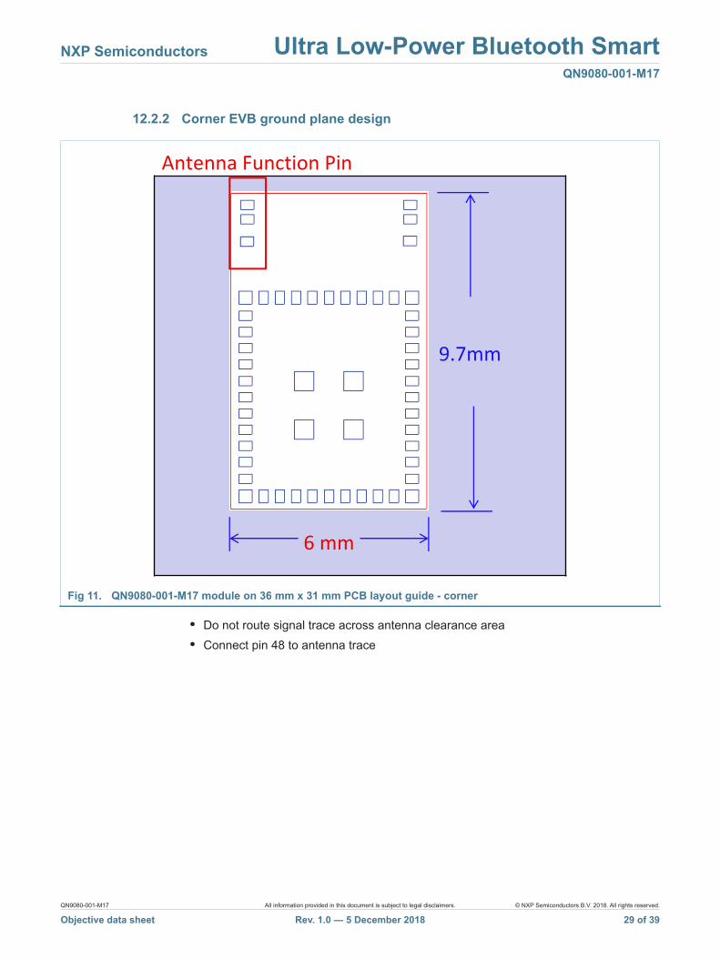
12.2.2 Corner EVB ground plane design
• Do not route signal trace across antenna clearance area• Connect pin 48 to antenna trace
Fig 11. QN9080-001-M17 module on 36 mm x 31 mm PCB layout guide - corner
9.7mm
6 mm
Antenna Function Pin
QN9080-001-M17 All information provided in this document is subject to legal disclaimers. © NXP Semiconductors B.V. 2018. All rights reserved.
Objective data sheet Rev. 1.0 — 5 December 2018 29 of 39

NXP Semiconductors Ultra Low-Power Bluetooth SmartQN9080-001-M17
Fig 12. QN9080-001-M17 module on 36 mm x 31 mm GND PCB layout guide - corner - clearance area
Layer 1
≥ 31mm
≥ 36mm
Ant. Trace
Trace route
Trace route
Trace route
0.25mm
3.5mm
Pin48
Fig 13. QN9080-001-M17 module on 36 mm x 31 mm GND PCB layout guide - corner - clearance area layer 1dimensions
G
F
I
K
EParameter Units : mm
A 0.5
B 4.34
C 0.5
D 1
E 1.5
F 1.5
G 2
H 2.9
I 3.5
J 0.25
K 0.25
Layer 1
H
J
AB C D
Parameter Units : mm
L 6.75
M 3.5
N 2
O 2.9
O
L
N
M
Layer 1
Antenna Clearance Area
QN9080-001-M17 All information provided in this document is subject to legal disclaimers. © NXP Semiconductors B.V. 2018. All rights reserved.
Objective data sheet Rev. 1.0 — 5 December 2018 30 of 39

NXP Semiconductors Ultra Low-Power Bluetooth SmartQN9080-001-M17
12.3 Reflow profileQN9080-001-M17 is an MSL3 and PSL R5G product. PSL has been defined based on the standard J-STD-075. For reflow soldering, it is requested to follow the reflow profile and the paste manufacturer's guidelines on peak flow temperature, soak times, time above liquid and ramp rates.
12.4 Soldering paste and cleaningNXP does not recommend to use a solder paste that requires the module and PCB assembly to be cleaned (rinsed in water) for the following reasons:
• Solder flux residues and water can be trapped by the PCB, can or components and result in short circuits
NXP recommends to use a 'no clean' solder paste for all its module products.
Fig 14. QN9080-001-M17 module on 36 mm x 31 mm GND PCB layout guide - corner - clearance area layers 2, 3, 4 dimensions
Parameter Units : mm
P 6.75
Q 2
R 2.9
S 5.5
Layer 2,3,4
R
P
S
Antenna Clearance Area
Q
Table 17. Recommended solder reflow profileTemperature range Time
Peak temperature: 255 C 10 s Max.Heating: 230 C or higher 30 s Max.Preheating: 150 C to 180 C 60-120 s
QN9080-001-M17 All information provided in this document is subject to legal disclaimers. © NXP Semiconductors B.V. 2018. All rights reserved.
Objective data sheet Rev. 1.0 — 5 December 2018 31 of 39

NXP Semiconductors Ultra Low-Power Bluetooth SmartQN9080-001-M17
13. Package outline
Fig 15. Package outline LFLGA54 (SOT1910-1)
QN9080-001-M17 All information provided in this document is subject to legal disclaimers. © NXP Semiconductors B.V. 2018. All rights reserved.
Objective data sheet Rev. 1.0 — 5 December 2018 32 of 39

NXP Semiconductors Ultra Low-Power Bluetooth SmartQN9080-001-M17
14. Abbreviations
Table 18. Abbreviations Acronym DescriptionADC Analog to Digital ConverterAES Advanced Encryption StandardAPI Application Program InterfaceCLK CLocKCRC Cyclic redundancy CheckCTS Clear-To-SendDC Direct currentDIO Digital Input OutputDMA Direct memory AccessEEPROM Electrically-Erasable Programmable Read Only MemoryFIFO First In First OutGPIO General Purpose Input OutputID IDentificationIF Intermediate frequencyIO Input OutputMSL Moisture sensitivity levelNVIC Nested Vector Interrupt ControllerPCB Printed-Circuit BoardPHY PHYsicalPOR Power-On ResetPWM Pulse Width ModulationRAM Random Access MemoryRC Remote ControlRF Radio FrequencyRoHS Restriction of Hazardous SubstancesRSSI Receive Signal Strength IndicationRTS Request-To-SendRX ReceivedSCL Serial CLockSDA Serial DatASMDs Surface Mount DevicesSPI-bus Serial Peripheral Interface -busSysTick System Tick timerTX Transmit
QN9080-001-M17 All information provided in this document is subject to legal disclaimers. © NXP Semiconductors B.V. 2018. All rights reserved.
Objective data sheet Rev. 1.0 — 5 December 2018 33 of 39

NXP Semiconductors Ultra Low-Power Bluetooth SmartQN9080-001-M17
15. References
[1] IEEE Std 802.15.4-2011 IEEE Standard for Information Technology Part 15.4 — Wireless Medium Access Control (MAC) and Physical Layer (PHY) Specifications for Low-Rate Wireless Personal Area Networks (LR-WPANs).
[2] Wireless Connectivity — http://www.nxp.com/products/wireless-connectivity:WIRELESS-CONNECTIVITY
QN9080-001-M17 All information provided in this document is subject to legal disclaimers. © NXP Semiconductors B.V. 2018. All rights reserved.
Objective data sheet Rev. 1.0 — 5 December 2018 34 of 39

NXP Semiconductors Ultra Low-Power Bluetooth SmartQN9080-001-M17
16. Revision history
Table 19. Revision history Document ID Release date Data sheet status Change notice SupersedesQN9080-001-M17 v1.0 20181205 Objective data sheet Public release -
QN9080-001-M17 All information provided in this document is subject to legal disclaimers. © NXP Semiconductors B.V. 2018. All rights reserved.
Objective data sheet Rev. 1.0 — 5 December 2018 35 of 39

NXP Semiconductors Ultra Low-Power Bluetooth SmartQN9080-001-M17
17. Legal information
17.1 Data sheet status
[1] Please consult the most recently issued document before initiating or completing a design.
[2] The term ‘short data sheet’ is explained in section “Definitions”.
[3] The product status of device(s) described in this document may have changed since this document was published and may differ in case of multiple devices. The latest product status information is available on the Internet at URL http://www.nxp.com.
17.2 DefinitionsDraft — The document is a draft version only. The content is still under internal review and subject to formal approval, which may result in modifications or additions. NXP Semiconductors does not give any representations or warranties as to the accuracy or completeness of information included herein and shall have no liability for the consequences of use of such information.
Short data sheet — A short data sheet is an extract from a full data sheet with the same product type number(s) and title. A short data sheet is intended for quick reference only and should not be relied upon to contain detailed and full information. For detailed and full information see the relevant full data sheet, which is available on request via the local NXP Semiconductors sales office. In case of any inconsistency or conflict with the short data sheet, the full data sheet shall prevail.
Product specification — The information and data provided in a Product data sheet shall define the specification of the product as agreed between NXP Semiconductors and its customer, unless NXP Semiconductors and customer have explicitly agreed otherwise in writing. In no event however, shall an agreement be valid in which the NXP Semiconductors product is deemed to offer functions and qualities beyond those described in the Product data sheet.
17.3 DisclaimersLimited warranty and liability — Information in this document is believed to be accurate and reliable. However, NXP Semiconductors does not give any representations or warranties, expressed or implied, as to the accuracy or completeness of such information and shall have no liability for the consequences of use of such information. NXP Semiconductors takes no responsibility for the content in this document if provided by an information source outside of NXP Semiconductors.
In no event shall NXP Semiconductors be liable for any indirect, incidental, punitive, special or consequential damages (including - without limitation - lost profits, lost savings, business interruption, costs related to the removal or replacement of any products or rework charges) whether or not such damages are based on tort (including negligence), warranty, breach of contract or any other legal theory.
Notwithstanding any damages that customer might incur for any reason whatsoever, NXP Semiconductors’ aggregate and cumulative liability towards customer for the products described herein shall be limited in accordance with the Terms and conditions of commercial sale of NXP Semiconductors.
Right to make changes — NXP Semiconductors reserves the right to make changes to information published in this document, including without limitation specifications and product descriptions, at any time and without notice. This document supersedes and replaces all information supplied prior to the publication hereof.
Suitability for use — NXP Semiconductors products are not designed, authorized or warranted to be suitable for use in life support, life-critical or safety-critical systems or equipment, nor in applications where failure or malfunction of an NXP Semiconductors product can reasonably be expected to result in personal injury, death or severe property or environmental damage. NXP Semiconductors and its suppliers accept no liability for inclusion and/or use of NXP Semiconductors products in such equipment or applications and therefore such inclusion and/or use is at the customer’s own risk.
Applications — Applications that are described herein for any of these products are for illustrative purposes only. NXP Semiconductors makes no representation or warranty that such applications will be suitable for the specified use without further testing or modification.
Customers are responsible for the design and operation of their applications and products using NXP Semiconductors products, and NXP Semiconductors accepts no liability for any assistance with applications or customer product design. It is customer’s sole responsibility to determine whether the NXP Semiconductors product is suitable and fit for the customer’s applications and products planned, as well as for the planned application and use of customer’s third party customer(s). Customers should provide appropriate design and operating safeguards to minimize the risks associated with their applications and products.
NXP Semiconductors does not accept any liability related to any default, damage, costs or problem which is based on any weakness or default in the customer’s applications or products, or the application or use by customer’s third party customer(s). Customer is responsible for doing all necessary testing for the customer’s applications and products using NXP Semiconductors products in order to avoid a default of the applications and the products or of the application or use by customer’s third party customer(s). NXP does not accept any liability in this respect.
Limiting values — Stress above one or more limiting values (as defined in the Absolute Maximum Ratings System of IEC 60134) will cause permanent damage to the device. Limiting values are stress ratings only and (proper) operation of the device at these or any other conditions above those given in the Recommended operating conditions section (if present) or the Characteristics sections of this document is not warranted. Constant or repeated exposure to limiting values will permanently and irreversibly affect the quality and reliability of the device.
Terms and conditions of commercial sale — NXP Semiconductors products are sold subject to the general terms and conditions of commercial sale, as published at http://www.nxp.com/profile/terms, unless otherwise agreed in a valid written individual agreement. In case an individual agreement is concluded only the terms and conditions of the respective agreement shall apply. NXP Semiconductors hereby expressly objects to applying the customer’s general terms and conditions with regard to the purchase of NXP Semiconductors products by customer.
No offer to sell or license — Nothing in this document may be interpreted or construed as an offer to sell products that is open for acceptance or the grant, conveyance or implication of any license under any copyrights, patents or other industrial or intellectual property rights.
Document status[1][2] Product status[3] Definition
Objective [short] data sheet Development This document contains data from the objective specification for product development.
Preliminary [short] data sheet Qualification This document contains data from the preliminary specification.
Product [short] data sheet Production This document contains the product specification.
QN9080-001-M17 All information provided in this document is subject to legal disclaimers. © NXP Semiconductors B.V. 2018. All rights reserved.
Objective data sheet Rev. 1.0 — 5 December 2018 36 of 39

NXP Semiconductors Ultra Low-Power Bluetooth SmartQN9080-001-M17
Export control — This document as well as the item(s) described herein may be subject to export control regulations. Export might require a prior authorization from competent authorities.
Quick reference data — The Quick reference data is an extract of the product data given in the Limiting values and Characteristics sections of this document, and as such is not complete, exhaustive or legally binding.
Non-automotive qualified products — Unless this data sheet expressly states that this specific NXP Semiconductors product is automotive qualified, the product is not suitable for automotive use. It is neither qualified nor tested in accordance with automotive testing or application requirements. NXP Semiconductors accepts no liability for inclusion and/or use of non-automotive qualified products in automotive equipment or applications.
In the event that customer uses the product for design-in and use in automotive applications to automotive specifications and standards, customer (a) shall use the product without NXP Semiconductors’ warranty of the product for such automotive applications, use and specifications, and (b) whenever customer uses the product for automotive applications beyond
NXP Semiconductors’ specifications such use shall be solely at customer’s own risk, and (c) customer fully indemnifies NXP Semiconductors for any liability, damages or failed product claims resulting from customer design and use of the product for automotive applications beyond NXP Semiconductors’ standard warranty and NXP Semiconductors’ product specifications.
Translations — A non-English (translated) version of a document is for reference only. The English version shall prevail in case of any discrepancy between the translated and English versions.
17.4 TrademarksNotice: All referenced brands, product names, service names and trademarks are the property of their respective owners.
I2C-bus — logo is a trademark of NXP Semiconductors N.V.
18. Contact information
For more information, please visit: http://www.nxp.comFor sales office addresses, please send an email to: [email protected]
QN9080-001-M17 All information provided in this document is subject to legal disclaimers. © NXP Semiconductors B.V. 2018. All rights reserved.
Objective data sheet Rev. 1.0 — 5 December 2018 37 of 39

NXP Semiconductors Ultra Low-Power Bluetooth SmartQN9080-001-M17
19. Tables
Table 1. Ordering information . . . . . . . . . . . . . . . . . . . . .5Table 2. Ordering options . . . . . . . . . . . . . . . . . . . . . . . .6Table 3. Marking codes . . . . . . . . . . . . . . . . . . . . . . . . . .6Table 4. Device revision table. . . . . . . . . . . . . . . . . . . . . .6Table 5. Pin description . . . . . . . . . . . . . . . . . . . . . . . . . .9Table 6. Termination of unused pins. . . . . . . . . . . . . . . .17Table 7. Pin states in different power modes . . . . . . . . .17Table 8. General operating conditions . . . . . . . . . . . . . .20Table 9. Static characteristics: Power consumption in
active modes. . . . . . . . . . . . . . . . . . . . . . . . . . .20Table 10. Static characteristics: Bluetooth LE power
consumption in active modes. . . . . . . . . . . . . . 20Table 11. Static characteristics: Power consumption in
sleep, and power-down modes . . . . . . . . . . . . 21Table 12. 32 MHz clock source characteristics . . . . . . . . 21Table 13. 32.768 kHz clock source characteristics . . . . . 21Table 14. Receiver characteristics . . . . . . . . . . . . . . . . . . 22Table 15. Transmitter characteristics . . . . . . . . . . . . . . . . 22Table 16. BOD static characteristics . . . . . . . . . . . . . . . . 23Table 17. Recommended solder reflow profile. . . . . . . . . 31Table 18. Abbreviations . . . . . . . . . . . . . . . . . . . . . . . . . 33Table 19. Revision history . . . . . . . . . . . . . . . . . . . . . . . . 35
20. Figures
Fig 1. QN9080-001-M17 package marking . . . . . . . . . . .6Fig 2. QN9080-001-M17 – high level HW block diagram7Fig 3. QN9080-001-M17 block diagram using external
antenna . . . . . . . . . . . . . . . . . . . . . . . . . . . . . . . . .8Fig 4. QN9080-001-M17 pinout diagram . . . . . . . . . . . . .9Fig 5. Footprint information for reflow soldering of SIPs 24Fig 6. QN9080-001-M17 chip with integrated 2.4 GHz
antenna / SIP clearance size (top view). . . . . . . .25Fig 7. QN9080-001-M17 module on 36 mm x 31 mm PCB
layout guide- center edge . . . . . . . . . . . . . . . . . .26Fig 8. QN9080-001-M17 module on 36 mm x 31 mm GND
PCB layout guide - center edge - clearance area 27Fig 9. QN9080-001-M17 module on 36 mm x 31 mm GND
PCB layout guide - center edge - clearance area layer 1 dimensions . . . . . . . . . . . . . . . . . . . . . . .27
Fig 10. QN9080-001-M17 module on 36 mm x 31 mm GND
PCB layout guide - center edge - clearance area layers 2, 3, 4 dimensions. . . . . . . . . . . . . . . . . . . 28
Fig 11. QN9080-001-M17 module on 36 mm x 31 mm PCB layout guide - corner . . . . . . . . . . . . . . . . . . . . . . 29
Fig 12. QN9080-001-M17 module on 36 mm x 31 mm GND PCB layout guide - corner - clearance area . . . . 30
Fig 13. QN9080-001-M17 module on 36 mm x 31 mm GND PCB layout guide - corner - clearance area layer 1dimensions . . . . . . . . . . . . . . . . . . . . . . . . . . . . . 30
Fig 14. QN9080-001-M17 module on 36 mm x 31 mm GND PCB layout guide - corner - clearance area layers 2, 3, 4 dimensions . . . . . . . . . . . . . . . . . . . . . . . . . . 31
Fig 15. Package outline LFLGA54 (SOT1910-1) . . . . . . 32
QN9080-001-M17 All information provided in this document is subject to legal disclaimers. © NXP Semiconductors B.V. 2018. All rights reserved.
Objective data sheet Rev. 1.0 — 5 December 2018 38 of 39

NXP Semiconductors Ultra Low-Power Bluetooth SmartQN9080-001-M17
21. Contents
1 General description . . . . . . . . . . . . . . . . . . . . . . 12 Features and benefits . . . . . . . . . . . . . . . . . . . . 12.1 Feature of QN9080. . . . . . . . . . . . . . . . . . . . . . 22.2 Features of NTAG. . . . . . . . . . . . . . . . . . . . . . . 42.3 Features of integrated 2.4 GHz antenna . . . . . 53 Applications . . . . . . . . . . . . . . . . . . . . . . . . . . . . 54 Ordering information . . . . . . . . . . . . . . . . . . . . . 55 Marking . . . . . . . . . . . . . . . . . . . . . . . . . . . . . . . . 66 Block diagram . . . . . . . . . . . . . . . . . . . . . . . . . . 77 Pinning information . . . . . . . . . . . . . . . . . . . . . . 97.1 Pinning . . . . . . . . . . . . . . . . . . . . . . . . . . . . . . . 97.2 Pin description . . . . . . . . . . . . . . . . . . . . . . . . . 97.2.1 Termination of unused pins. . . . . . . . . . . . . . . 167.2.2 Pin states in different power modes . . . . . . . . 178 Compliance statements and documentation 178.1 FCC Statements and documentation . . . . . . . 178.1.1 FCC interference Statements . . . . . . . . . . . . . 178.1.2 FCC end product labelling . . . . . . . . . . . . . . . 188.2 Industry Canada Statement . . . . . . . . . . . . . . 198.2.1 . . . . Industry of Canada end product labelling 198.3 Japanese Radio Certification Statement . . . . 198.3.1 Radio Certification end product labelling . . . . 199 Static characteristics. . . . . . . . . . . . . . . . . . . . 209.1 General operating conditions . . . . . . . . . . . . . 209.2 Power consumption . . . . . . . . . . . . . . . . . . . . 209.3 Clock source . . . . . . . . . . . . . . . . . . . . . . . . . . 2110 RF characteristics . . . . . . . . . . . . . . . . . . . . . . 22
10.1 Receiver . . . . . . . . . . . . . . . . . . . . . . . . . . . . . 2210.2 Transmitter . . . . . . . . . . . . . . . . . . . . . . . . . . . 2211 Internal antenna characteristic . . . . . . . . . . . 2312 Layout guideline . . . . . . . . . . . . . . . . . . . . . . . 2412.1 Footprint information for reflow soldering. . . . 2412.2 Layout recommendation for ground plane
implementation and clearance area for QN9080-001-M17 with integrated 2.4 GHz antenna . . . . . . . . . . . . . . . . . . . . . . . . . . . . . 25
12.2.1 Center edge PCB ground plane design . . . . . 2612.2.2 Corner EVB ground plane design . . . . . . . . . 2912.3 Reflow profile . . . . . . . . . . . . . . . . . . . . . . . . . 3112.4 Soldering paste and cleaning. . . . . . . . . . . . . 3113 Package outline . . . . . . . . . . . . . . . . . . . . . . . . 3214 Abbreviations . . . . . . . . . . . . . . . . . . . . . . . . . 3315 References . . . . . . . . . . . . . . . . . . . . . . . . . . . . 3416 Revision history . . . . . . . . . . . . . . . . . . . . . . . 3517 Legal information . . . . . . . . . . . . . . . . . . . . . . 3617.1 Data sheet status . . . . . . . . . . . . . . . . . . . . . . 3617.2 Definitions . . . . . . . . . . . . . . . . . . . . . . . . . . . 3617.3 Disclaimers. . . . . . . . . . . . . . . . . . . . . . . . . . . 3617.4 Trademarks . . . . . . . . . . . . . . . . . . . . . . . . . . 3718 Contact information . . . . . . . . . . . . . . . . . . . . 3719 Tables . . . . . . . . . . . . . . . . . . . . . . . . . . . . . . . . 3820 Figures . . . . . . . . . . . . . . . . . . . . . . . . . . . . . . . 3821 Contents. . . . . . . . . . . . . . . . . . . . . . . . . . . . . . 39
© NXP Semiconductors B.V. 2018. All rights reserved.For more information, please visit: http://www.nxp.comFor sales office addresses, please send an email to: [email protected]
Date of release: 5 December 2018Document identifier: QN9080-001-M17
Please be aware that important notices concerning this document and the product(s)described herein, have been included in section ‘Legal information’.