Embed Size (px)
Citation preview

Massimo Alioto
Ultra-Low Power Design Approaches for IoT
National University of Singapore (NUS)
ECE Department
Green IC group

2 Prof. Massimo Alioto
Outline IoT: the context
Ultra-low voltage operation
Design Issues and Solutions at Ultra-Low Voltages
performance
leakage
variations and resiliency
Conclusions

3 Prof. Massimo Alioto
Internet of Things:
The Context

4
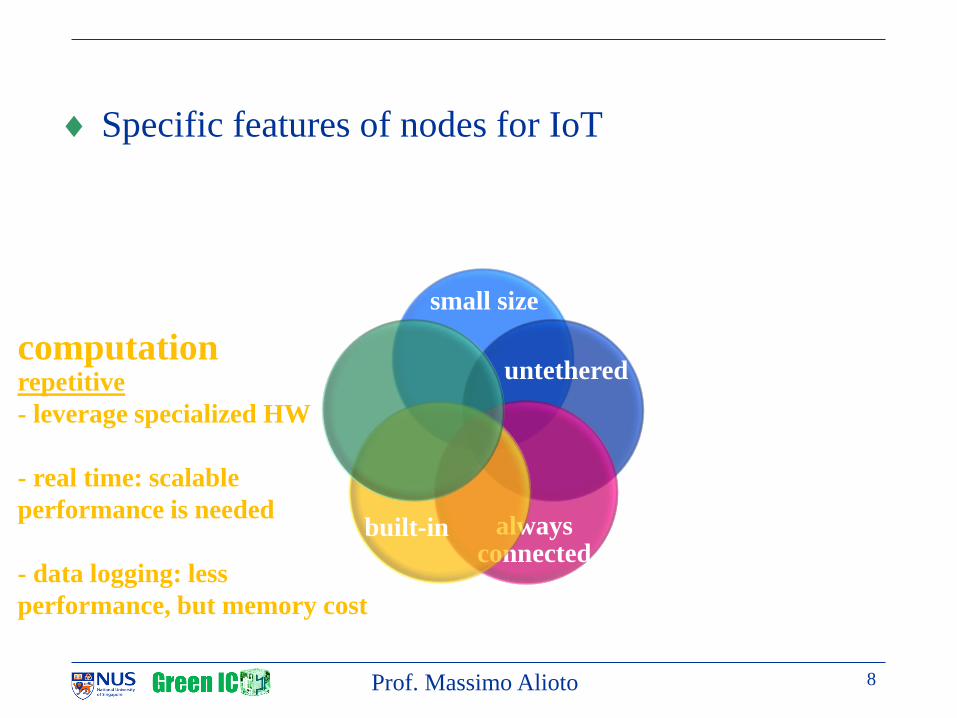
Specific features of nodes for IoT
Nodes for the Internet of Things: Peculiarities
Prof. Massimo Alioto
small size
untethered
always connected
built-in
wireless
IoT node
form factor
power connection communication
processing availability

5
Specific features of nodes for IoT
Prof. Massimo Alioto
small size
1-100 mm3
(battery, energy scavenger)

6
Specific features of nodes for IoT
Prof. Massimo Alioto
small size
untethered
self-powered
(limited power)
Ws (perpetual)
100 nW (10 yrs)
t
available
energy
no
operationnormal
operation
normal
operation
no
operation
dark silicon
40 W (1 week)

7
Specific features of nodes for IoT
Prof. Massimo Alioto
small size
untethered
always connected
duty cycled
active mode
sleep mode
active mode
sleep mode
Twkup
8
Specific features of nodes for IoT
Prof. Massimo Alioto
small size
untethered
always connected
built-in
computation repetitive
- leverage specialized HW
- real time: scalable
performance is needed
- data logging: less
performance, but memory cost

9
Specific features of nodes for IoT
Prof. Massimo Alioto
small size
untethered
always connected
built-in
wireless
communication computation vs
communication tradeoff
- data representation
(compressive sensing,
compression)
- limit TX to critical events
or significant changes
(critical event monitoring)

10
Power vs Energy
Prof. Massimo Alioto
Duty cycled systems with limited power
active only periodically (or on demand) for a short time
partition into always-on block (timers, retentive memory) and
duty cycled blocks (all others, active 0.1-1% of the time)
active mode
sleep mode
active mode
sleep mode
Twkup
wkupactiveonalwaysavg TEPP /
[RJA12] M. Alioto, et Al., “Active RFID: A Perpetual Wireless Communications Platform
for Sensors,” ESSCIRC 2012

11 Prof. Massimo Alioto
minimum power is the goal for always-on block
minimize power, essentially
leakage (dynamic power very small
– little active and slow)
minimum energy per operation is the goal for duty-
cycled blocks
minimize energy per operation
(dynamic + leakage energy)
1/X duty cycling increases energy
budget by X
in both cases, ultra-low voltage operation is absolutely needed
VDD
power
VTH
target
VDD
energy
VTH
minimum
energy point
VDD,opt
target

12 Prof. Massimo Alioto
Ultra-Low Voltage Operation

13
Voltage scaling is a powerful knob to improve
energy efficiency
quadratic benefit, if dynamic energy CV2 dominates
performance degradation
How aggressively
should we scale VDD?
energy-performance tradeoff
NT: relatively good speed
nearly min. energy,
ST: low speed, min. power
Prof. Massimo Alioto
Operation at Ultra-Low Voltages (ULV)
VTH
quadra
tic e
nergy
benef
it
MEP
linear performance
degradation
exp. p
erfo
rman
ce
deg
radat
ion
energy
degradation
near threshold
(NT)above thresholdsubthreshold
(ST)
performance
energy

14
Example: first mm3 system
transistors in weak (ST) or moderate (NT) inversion
ITRS: VDD, VTH constant
Prof. Massimo Alioto
weak inversion
moderate inversion
strong inversion
400-600 mV <400 mV
00.10.20.30.40.50.60.70.80.9
1
20
13
20
14
20
15
20
16
20
17
20
18
20
19
20
20
20
21
20
22
20
23
20
24
20
25
20
26
20
27
20
28
VD
D, V
TH
(V)
year
[CGH11] G. Chen, et Al., “A 1 Cubic Millimeter Energy-Autonomous
Wireless Intraocular Pressure Monitor,” ISSCC 2011

15
Gate delay: CVDD/2Ion
Ion defines performance
ION EKV model (transregional) [EV06]
Inversion Coefficient vs gate overdrive
Prof. Massimo Alioto
Performance @ ULV: Transistor On-Current
𝐼𝐶 =𝐼𝑜𝑛𝐼0
= ln 𝑒𝑣 + 1 2 𝐼0 = 2 ⋅ 𝑛 ⋅ 𝜇 ⋅ 𝐶𝑂𝑋
𝑊
𝐿𝑣𝑡2
𝑣 =𝑉𝐷𝐷 − 𝑉𝑇𝐻2 ⋅ 𝑛 ⋅ 𝑣𝑡
IC < 0.1 IC > 10 0.1 IC 10
[EV06] C. Enz, E. Vittoz, Charge-Based MOS Transistor Modeling (...), Wiley, 2006
weak inversion
moderate inversion
strong inversion
VDD
Ion
C
gate delay

16
ION vs VDD: steep (superlinear) in NT and ST
performance sensitive
to both VDD and VTH
choice of VTH
really critical
sensitivity to VDD,
VTH variations...
Prof. Massimo Alioto
region VDD on current
weak inversion sub threshold 𝑰𝒐𝒏 ≈ 𝑰𝟎 ⋅ 𝒆
𝑽𝑫𝑫−𝑽𝑻𝑯𝒏⋅𝒗𝒕
moderate inversion near threshold 𝑰𝒐𝒏 ≈ 𝟎. 𝟓𝟒 ⋅ 𝑰𝟎 ⋅ 𝒗 + 𝟎. 𝟖𝟖 𝟐
strong inversion above threshold 𝐼𝑜𝑛 ≈ 𝐼0 ⋅ 𝑣𝛼 (1)
1E-06
1E-05
1E-04
1E-03
1E-02
1E-01
1E+00
0 200 400 600 800 1000 1200
I on
no
rmal
ize
d t
o L
VT
NM
OS
@ n
om
inal
VD
D
VDD [mV]
linear

17
Performance: fan-out-4 delay (FO4)
speed of technology and ()architecture
Prof. Massimo Alioto
1E+00
1E+01
1E+02
1E+03
1E+04
0 200 400 600 800 1000 1200
no
rmal
ized
FO
4 d
elay
VDD [mV]
LVT RVT
20
4
10
𝑇𝐶𝐾 = 𝐿𝐷𝑒𝑓𝑓 ⋅ 𝐹𝑂4
effective logic depth
FO4
TCLK
D
Q
Q
Clk D
Q
Q
Clk ...
1 order of magnitude slower than nominal voltage
2-4 orders of magnitude slower

18
Leveraging high sensitivity of Ion to VDD @ NT
VDD powerful knob to dynamically improve performance
performance improvement due to V=100-mV boosting
ST: more effective, pretty useless (low performance anyway)
NT: effective and low energy cost (V is small fraction of VDD)
Prof. Massimo Alioto
VDD FO4 improvement
200 mV 7.5X
400 mV 3.6X
600 mV 1.6X
800 mV 1.2X
1 V 1.1X
ST: 8X improvement/100 mV
NT: 2-4X improvement/100 mV
19
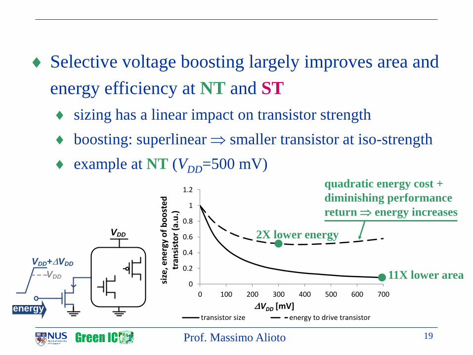
Selective voltage boosting largely improves area and
energy efficiency at NT and ST
sizing has a linear impact on transistor strength
boosting: superlinear smaller transistor at iso-strength
example at NT (VDD=500 mV)
Prof. Massimo Alioto
0
0.2
0.4
0.6
0.8
1
1.2
0 100 200 300 400 500 600 700
size
, en
erg
y o
f b
oo
ste
d
tran
sist
or
(a.u
.)
VDD [mV]transistor size energy to drive transistor
2X lower energy
11X lower area
quadratic energy cost +
diminishing performance
return energy increases
VDD
VDD
VDD+VDD
energy

20 Prof. Massimo Alioto
Design Issues and Solutions
at Ultra-Low Voltages: Performance

21 Prof. Massimo Alioto
Performance at NT/ST worse than nominal voltage
can be acceptable in practical situations
tasks of IoT nodes are often relatively simple
example of typical throughput: few hundreds of MOPS (e.g.,
video processing) down to kOPS (e.g., temper. monitoring)
Wire delay at NT/ST
gate delay much less critical
than nominal VDD
design as in the “good old days”
Performance Degradation
...
wire delay
de
lay
VDD

22 Prof. Massimo Alioto
If higher performance is sometimes needed...
wide voltage scaling
(e.g., from 400 mV to 1.2 V)
large performance improvement (10X)
energy/op increases quadratically (9X)
tolerable if occasional
optimized for NT
energy/performance tradeoff
at 1.2 V is degraded by 25%
1 10 400 mV
1.2 V
𝐸𝑑𝑦𝑛𝐶 ⋅ 𝑉𝐷𝐷2
[J12] S. Jain, et Al., IEEE ISSCC Dig. Tech. Papers, pp. 66–67, Feb. 2012
23 Prof. Massimo Alioto
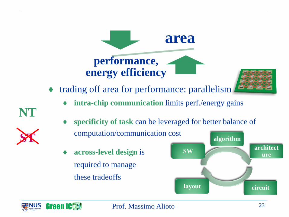
trading off area for performance: parallelism
intra-chip communication limits perf./energy gains
specificity of task can be leveraged for better balance of
computation/communication cost
across-level design is
required to manage
these tradeoffs
area
performance, energy efficiency
layout
SW
algorithm
architecture
circuit
NT
ST

24 Prof. Massimo Alioto
trading off area for performance: specialized HW
example: FFT, Java processor,
AES, MPEG decoder...
specialized HW has better
performance/energy tradeoff
than general-purpose
larger benefit for recurrent and specific tasks
area
performance, energy efficiency

25 Prof. Massimo Alioto
Design Issues and Solutions
at Ultra-Low Voltages: Leakage

26
If dynamic energy per operation dominates:
reduce VDD as much as possible
energy reduction limited by VDD,min (defined by robustness
issues, very different for logic and memory)
Prof. Massimo Alioto
Energy vs VDD
VDD
E
VDD,min
Edyn
VDD
(mV)
VDD2 energy
saving
including
Cg(VDD)
200 mV 36X 54X
400 mV 9X 11.6X
600 mV 4X 4.4X
800 mV 2.2X 2.4X
1 V 1.4X 1.4X
1.2 V 1X 1X
𝐸𝑑𝑦𝑛 = 𝛼𝑆𝑊 ⋅ 𝐶 ⋅ 𝑉𝐷𝐷2
27
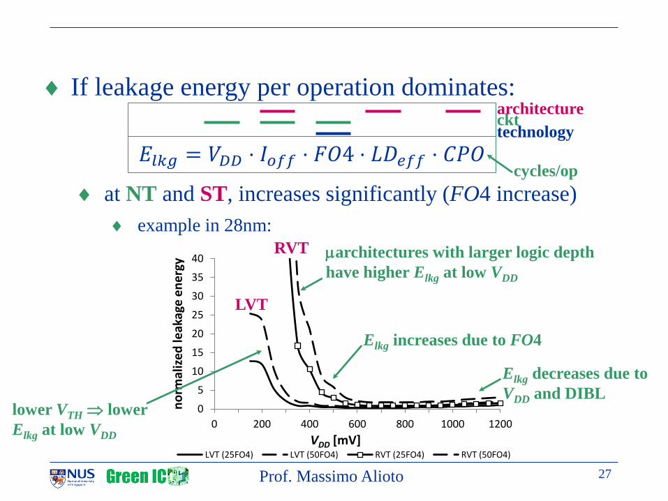
If leakage energy per operation dominates:
at NT and ST, increases significantly (FO4 increase)
example in 28nm:
Prof. Massimo Alioto
𝐸𝑙𝑘𝑔 = 𝑉𝐷𝐷 ⋅ 𝐼𝑜𝑓𝑓 ⋅ 𝐹𝑂4 ⋅ 𝐿𝐷𝑒𝑓𝑓 ⋅ 𝐶𝑃𝑂
0
5
10
15
20
25
30
35
40
0 200 400 600 800 1000 1200
no
rmal
ize
d le
akag
e e
ne
rgy
VDD [mV]LVT (25FO4) LVT (50FO4) RVT (25FO4) RVT (50FO4)
lower VTH lower
Elkg at low VDD
architectures with larger logic depth
have higher Elkg at low VDD
Elkg decreases due to
VDD and DIBL
Elkg increases due to FO4
RVT
LVT
cycles/op
technology
ckt
architecture

28
Combining dynamic and leakage energy
minimum energy point (MEP)
relatively flat (VDD mainly set by performance target)
can lie in either NT or ST
time varying: depends on temperature, data set...
Prof. Massimo Alioto
VDD
E
VDD,min
Edyn
Elkg
ETOT
MEP
VDD,opt
Emin
Minimum Energy Point

29
Leakage energy takes up increasingly larger fraction of
total energy at lower VDD
at low VDD, leakage energy increases exponentially, dynamic
energy decreases quadratically
ex.: processor with L1 cache (VDDcache,min=0.55 V)
Prof. Massimo Alioto
42% 95% 14%
[J12] S. Jain, et Al., IEEE ISSCC Dig. Tech. Papers, pp. 66–67, Feb. 2012

30
Leakage is truly critical (process not enough)
large, limits energy reduction
Several traditional circuit techniques do not work...
transistor stacking is ineffective
Prof. Massimo Alioto
Traditional Techniques for Low Leakage
1
10
100
0 200 400 600 800 1000 1200
I on
and
I off
stac
kin
g fa
cto
r
VDD [mV]
LVT NMOS
Ion (2-stacked) Ion (3-stacked) Ion (4-stacked)
Ioff (2-stacked) Ioff (3-stacked) Ioff (4-stacked)
3X 20X
1X
1
1
1
1

31
power gating is much less effective (Ion/Ioff degradation)
typical leakage reduction: 10-100X
NT: small leakage reduction, ST: no leakage reduction at all
solution: boost gate voltage of sleep transistor (increases Ion/Ioff)
Prof. Massimo Alioto
1E+0
1E+1
1E+2
1E+3
1E+4
1E+5
1E+6
1E+7
1E+0
1E+1
1E+2
1E+3
1E+4
1E+5
1E+6
1E+7
1E+8
0 200 400 600 800 1000 1200 de
grad
atio
n in
I off
red
uct
ion
w
.r.t
. no
min
al V
DD
I on/I
off
no
rmal
ize
d t
o
no
min
al V
DD
VDD [mV]
degradation in Ioff reductiondegradation in leakage reduction w.r.t. nominal VDD
VDD
sleep
transistor
sleep
selective voltage boosting

32
multi-VTH actually degrades energy efficiency
delay sensitive to VTH critical path changes at scaled VDD
double energy penalty
compared to single-VTH
Prof. Massimo Alioto
VDD=0.6 V HVT
LVT VDD=0.4 V
𝐸𝑙𝑘𝑔 = 𝑉𝐷𝐷 ⋅ 𝐼𝑜𝑓𝑓 ⋅ 𝑇𝐶𝐾 ⋅ 𝐶𝑃𝑂
larger than single-(low)VTH
larger than single-(high)VTH
0
0.05
0.1
0.15
0.2
0.25
0 200 400 600 800 1000 1200
no
rmal
ize
d e
ne
rgy
VDD [mV]multi-VTH LVT LVT+100 mV
LVT
MEP1=(350 mV, 0.087)MEP2=(350 mV, 0.089)MEP3=(450 mV, 0.13)
LVT+100 mV
1.5X

33
Leakage reduction at ULV: alternative approaches
fine-grain power gating
disable unused blocks at runtime
small quickly and frequently
overhead: multiple sleep
transistors, isolation, control
lower control overhead via ckt/architectural support for SW
fine-grain voltage domains
Elkg reduced at lower VDD (e.g., 2X/100 mV)
selectively reduce VDD wherever possible (slower)
similar considerations as power gating
Prof. Massimo Alioto
VDD
sleep
transistor
sleep
VDD,H VDD,L VDD,L
VDD,L VDD,H VDD,L
Counteracting Leakage at ULV

34
microarchitecture-circuit co-design: pipelining
use deep pipelines + refined circuit
techniques/methodologies to deal with
clocking overhead
example: 17FO4/stage in FFT engine
(30MHz @ 0.27V, 4X less energy than state of the art)
Prof. Massimo Alioto
𝐸𝑙𝑘𝑔 = 𝑉𝐷𝐷 ⋅ 𝐼𝑜𝑓𝑓 ⋅ 𝐹𝑂4 ⋅ 𝑳𝑫𝒆𝒇𝒇 ⋅ 𝐶𝑃𝑂
clk clk
D Q
combinational block D Q
Reg Reg
D Q
clk
Reg comb 1 D Q
clk
Reg comb 2 D Q
clk
Reg comb n D Q
clk
Reg ...
stage 1 stage 2 stage n
LD LD LD
PIPESTAGE LOGIC
TCLK
CLOCKING OVERHEAD
[AJC11] M. Seok, et Al. “A 0.27V, 30MHz, 17.7nJ/transform 1024-pt complex FFT core with
super-pipelining,” ISSCC 2011
leakage/clocking
energy tradeoff

35
VTH selection
energy-optimal VDD,opt
is independent of VTH
choose VTH according
to performance target
body biasing
makes sense in FDSOI (VTH sensitivity to VBB large enough)
Prof. Massimo Alioto
0
0.05
0.1
0.15
0.2
0.25
0 200 400 600 800 1000 1200
no
rmal
ize
d e
ne
rgy
VDD [mV]LVT-100 mV LVT LVT+100 mV
VTH
MEP1=(350 mV, 0.086)MEP2=(350 mV, 0.066)MEP3=(350 mV, 0.064)
[A12] M. Alioto, “Ultra-Low Power VLSI Circuit Design
Demystified and Explained: A Tutorial,” IEEE TCAS-I, Jan. 2012.
36 Prof. Massimo Alioto
Design Issues and Solutions at Ultra-Low
Voltages: Variability and Resiliency

37 Prof. Massimo Alioto
Variations: Why do They Matter?
Resiliency degraded at ULV
process/voltage/temperature
larger than at nominal VDD
ageing, soft errors...
design margining
cycle margin
(20-30% @ full VDD)
degrades performance
AND energy efficiency
large energy penalty
0
5
10
15
200 400 600 800 1000
s/
of
FO4
no
rma
lize
d t
o t
he
ca
se V
DD=
1 V
VDD (mV)
subthreshold
near
threshold
above threshold
nominal margin
pro
cess
vo
ltag
e
tem
pera
ture
ag
ing
[A12] M. Alioto, “Ultra-Low Power VLSI Circuit Design Demystified and Explained: A
Tutorial,” IEEE TCAS-I, Jan. 2012.
0
0.05
0.1
0.15
0.2
0
0.5
1
1.5
2
1.1 1.2 1.3 1.4 1.5 1.6 1.7 1.8 1.9 2
req
'd v
olt
age
incr
eas
e (
V)
en
erg
y in
cre
ase
fact
or
cycle time margin
VDD=400 mV VDD=600 mV VDD=400 mV VDD=600 mV
38 Prof. Massimo Alioto
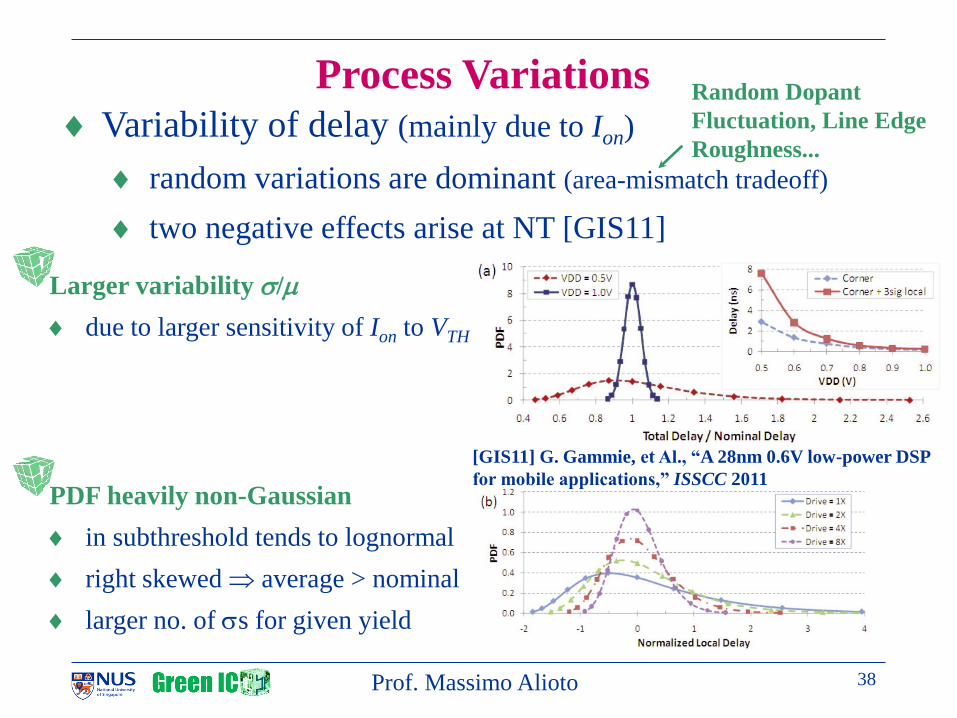
Process Variations
Larger variability s/
due to larger sensitivity of Ion to VTH
PDF heavily non-Gaussian
in subthreshold tends to lognormal
right skewed average > nominal
larger no. of ss for given yield
Variability of delay (mainly due to Ion)
random variations are dominant (area-mismatch tradeoff)
two negative effects arise at NT [GIS11]
Random Dopant
Fluctuation, Line Edge
Roughness...
[GIS11] G. Gammie, et Al., “A 28nm 0.6V low-power DSP
for mobile applications,” ISSCC 2011

39 Prof. Massimo Alioto
Semi-quantitative analysis of Ion variations
at NT, s/ is intermediate (4-5X)
no. of std deviations (yield)
at NT: somewhat intermediate
ex. @ 3s for single gate:
margin = 10s/ = 300%
𝐼𝑜𝑛 ∝ 1 −Δ𝑉𝑇𝐻
𝑉𝐷𝐷 − 𝑉𝑇𝐻 𝐼𝑜𝑛 ∝ 𝑒
−Δ𝑉𝑇𝐻𝑛⋅𝑣𝑡
𝜎𝐼𝑜𝑛𝜇𝐼𝑜𝑛
=𝜎𝑉𝑇𝐻
𝑉𝐷𝐷 − 𝑉𝑇𝐻
𝜎𝐼𝑜𝑛𝜇𝐼𝑜𝑛
= 𝑒𝜎𝑉𝑇𝐻𝑛⋅𝑣𝑡
2
− 1
Above threshold
ex. VDD=0.9 V, VTH=0.36 V, sVTH=35 mV
6.5%
Subthreshold
ex. sVTH=35 mV, n=1.35
131% (20X)
YIELD Gaussian lognormal
84% s es
97.7% 2s e2s7.4s
99.9% 3s e3s20.1s
La
rger
va
riab
ilit
y s
/
La
rger
no
. o
f s

40
Variability/leakage tradeoff unavoidable
averaging effect reduces variability by
cascaded
logic gates
stacked
transistors
larger transistors
path delay variability from FO4 variability (min. sized)
Prof. Massimo Alioto
𝑛𝜎𝜎𝑝𝑎𝑡ℎ𝑑𝑒𝑙𝑎𝑦
𝜇𝑝𝑎𝑡ℎ𝑑𝑒𝑙𝑎𝑦= 𝑛𝜎
𝜎𝐹𝑂4,𝐷2𝐷𝜇𝐹𝑂4,𝐷2𝐷
2
+
𝜎𝐹𝑂4,𝑟𝑎𝑛𝑑𝑜𝑚𝜇𝐹𝑂4,𝑟𝑎𝑛𝑑𝑜𝑚
2
𝑵𝒈𝒂𝒕𝒆 ⋅ 𝒔𝒕𝒓𝒆𝒏𝒈𝒕𝒉 ⋅ 𝑵𝒔𝒕𝒂𝒄𝒌𝒆𝒅
strength
stacking
cascading ...1 2 3 Ngate
𝝈
𝝁=
𝟏
𝑵𝒈𝒂𝒕𝒆
𝝈
𝝁=
𝟏
𝑵𝒔𝒕𝒂𝒄𝒌𝒆𝒅
𝝈
𝝁=
𝟏
𝒔𝒕𝒓𝒆𝒏𝒈𝒕𝒉
21 Nstacked
...
strength W/Wmin
L=Lmin
[MWA10] M. Merrett, et Al., “Design Metrics for RTL Level Estimation of Delay Variability Due to
Intradie (Random) Variations,” ISCAS 2010

41
Delay is very sensitive to VDD and temperature
voltage: up to 30-50% margin
temperature: up to 100% margin
NT systems require adaptive schemes
sense VDD and T and adjust clock cycle
can compensate slow variations (margin needed for fast)
Prof. Massimo Alioto
Voltage/Temperature Variations
0
0.05
0.1
0.15
0.2
0.25
0 200 400 600 800 1000 1200
no
rmal
ize
d e
ne
rgy
VDD [mV]
LVT-100 mV
25FO4 (27oC) 50FO4 (27oC) 100FO4 (27oC)25FO4 (70Oc) 50FO4 (70oC) 100FO4 (70oC)
VTH
1.69X larger
Emin 1.36X larger
Emin 1.37X larger
Emin
1
1.1
1.2
1.3
1.4
1.5
1.6
0 200 400 600 800 1000 1200
cycl
e t
ime
mar
gin
VDD [mV]5% VDD droop 10% VDD droop

42 Prof. Massimo Alioto
Compensation of variations at different times
tradeoff between energy cost of margining vs energy cost
to reduce amount of margin
large variations at NT/ST: runtime compensation usually
required
detect timing errors/correct: minimum or no margin at all
clock cycle margin to deal with design uncertainty sources:
time at which LUT is updated
process variations agingtemperature/slow
VDD variationsfast
variationstotal clock cycle
marginimplementation
complexity/area overhead
design time
testing time
boot time
periodically @runtime
nominal clock cycle clock cycle margin
margined clock cycle
runtime
Clock Cycle Margin Reduction/Elimination

43 prof. Massimo Alioto
Margin Elimination: Timing Error Detection
Reduce/eliminate worst-case
margin by catching delay faults
correct at run-time, tune to compensate actual variations
nominal margin
pro
cess
vo
ltag
e
tem
pera
ture
ag
ing
In-situ monitoring
P, V, T, aging, fast
variations
no margin
invasive, limited tuning
Fault prediction (Tunable Replica Circuit)
partially: P, V, T, aging, fast (not soft errors)
needs some margin (false positives,
mimics only critical path)
little invasive, tuning required, low overhead
D FF
Q
timing
sensorerror
CLK
CLK
error = 0 error = 1
CLK
D D
tSETUP
D FF
Q
CLKcritical path
MATCHED DELAY
errorD FF
Q
CLK
TRC CHECKER
tuning

44 prof. Massimo Alioto
Margin Elimination: Error Correction
Faults can be corrected at various levels
across-level design/optimization/control needed
energy overhead
testing is painful (long, tuning)
SW Architecture Microarchitecture Circuit
faster correction
Circuit Microarchitecture Architecture SW
less HW resources
SW Architecture Microarchitecture Circuit
lower energy/performance penalty
2 DDcorrection VCfrateerrorEE

45 prof. Massimo Alioto
Approximate Computing: Negative Margining
Some apps do not need to have perfect computation
approximate computing (deterministic, voltage overscaling)
ex.: multimedia, sensor fusion
avg error rate kept within bound (slow correction loop)
ex.: our first SRAM with Dynamically Adjustable Error-Quality
quality
energy
OS
HW
sensors (context)
energy-quality knobs
quality
[FKB14] F. Frustaci, et Al., “A 32kb SRAM for Error-Free and Error-Tolerant Applications
with Dynamic Energy-Quality Management in 28nm CMOS,” ISSCC 2014
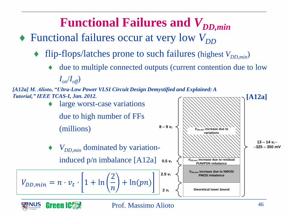
46
Functional failures occur at very low VDD
flip-flops/latches prone to such failures (highest VDD,min)
due to multiple connected outputs (current contention due to low
Ion/Ioff)
large worst-case variations
due to high number of FFs
(millions)
VDD,min dominated by variation-
induced p/n imbalance [A12a]
Prof. Massimo Alioto
Functional Failures and VDD,min
theoretical lower bound
VDD,min increase due to NMOS/
PMOS imbalance
VDD,min increase due to
variations
VDD,min increase due to residual
PUN/PDN imbalance
8 – 9 vt
0.5 vt
2.5 vt
2 vt
13 – 14 vt
325 – 350 mV
[A12a]
𝑉𝐷𝐷,𝑚𝑖𝑛 = 𝑛 ⋅ 𝑣𝑡 ⋅ 1 + ln2
𝑛+ ln(𝑝𝑛)
[A12a] M. Alioto, “Ultra-Low Power VLSI Circuit Design Demystified and Explained: A
Tutorial,” IEEE TCAS-I, Jan. 2012.

47
SRAM more vulnerable than logic
read/write/hold margins set by
strength ratio
no averaging across multiple cells,
as opposed to logic
reducing VDD,min of SRAMs at different levels
within the cell: VTH adjustment, lithography-friendly layout,
circuit (sizing, more robust topologies)
outside the cell: array architecture, assist techniques
Prof. Massimo Alioto
READ WRITE
VDDVDD
M1
M2
M3
M4
M5
M6
M7
WWL WWLWBL WBL RBL
M8RWL
1 1
2-2.5
1.5-1.8
3-4
V1
V2
2-2.5
1.5-1.8
4-5
6T 6T 6T 6T 6T 6T 6T 6T
6T 6T 6T 6T 6T 6T 6T 6T
6T 6T 6T 6T 6T 6T 6T 6T
6T 6T 6T 6T 6T 6T 6T 6T
6T 6T 6T 6T 6T 6T 6T 6T
6T 6T 6T 6T 6T 6T 6T 6T
6T 6T 6T 6T 6T 6T 6T 6T
6T 6T 6T 6T 6T 6T 6T 6T
col. decoding, BL
conditioning, senseamps
latches, I/O...
6T 6T 6T 6T 6T 6T 6T 6T
6T 6T 6T 6T 6T 6T 6T 6T
6T 6T 6T 6T 6T 6T 6T 6T
6T 6T 6T 6T 6T 6T 6T 6T
6T 6T 6T 6T 6T 6T 6T 6T
6T 6T 6T 6T 6T 6T 6T 6T
6T 6T 6T 6T 6T 6T 6T 6T
6T 6T 6T 6T 6T 6T 6T 6T
col. decoding, BL
conditioning, senseamps
latches, I/O...
ca
ch
e
co
ntr
olle
r
cache interface
6T 6T 6T 6T 6T 6T 6T 6T
6T 6T 6T 6T 6T 6T 6T 6T
6T 6T 6T 6T 6T 6T 6T 6T
6T 6T 6T 6T 6T 6T 6T 6T
6T 6T 6T 6T 6T 6T 6T 6T
6T 6T 6T 6T 6T 6T 6T 6T
6T 6T 6T 6T 6T 6T 6T 6T
6T 6T 6T 6T 6T 6T 6T 6T
row
de
co
de
r
col. decoding, BL
conditioning, senseamps
WL
bu
ffe
rs
timing, control
signals
latches, I/O...
48
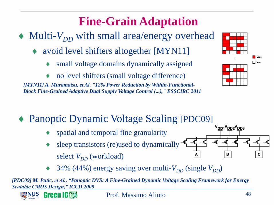
Multi-VDD with small area/energy overhead
avoid level shifters altogether [MYN11]
small voltage domains dynamically assigned
no level shifters (small voltage difference)
Panoptic Dynamic Voltage Scaling [PDC09]
spatial and temporal fine granularity
sleep transistors (re)used to dynamically
select VDD (workload)
34% (44%) energy saving over multi-VDD (single VDD)
Prof. Massimo Alioto
Fine-Grain Adaptation
[MYN11] A. Muramatsu, et Al. "12% Power Reduction by Within-Functional-
Block Fine-Grained Adaptive Dual Supply Voltage Control (...)," ESSCIRC 2011
[PDC09] M. Putic, et Al., “Panoptic DVS: A Fine-Grained Dynamic Voltage Scaling Framework for Energy
Scalable CMOS Design,” ICCD 2009
49
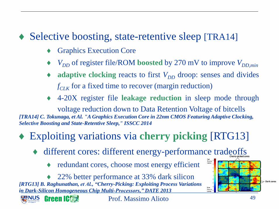
Selective boosting, state-retentive sleep [TRA14]
Graphics Execution Core
VDD of register file/ROM boosted by 270 mV to improve VDD,min
adaptive clocking reacts to first VDD droop: senses and divides
fCLK for a fixed time to recover (margin reduction)
4-20X register file leakage reduction in sleep mode through
voltage reduction down to Data Retention Voltage of bitcells
Exploiting variations via cherry picking [RTG13]
different cores: different energy-performance tradeoffs
redundant cores, choose most energy efficient
22% better performance at 33% dark silicon
Prof. Massimo Alioto
[TRA14] C. Tokunaga, et Al. "A Graphics Execution Core in 22nm CMOS Featuring Adaptive Clocking,
Selective Boosting and State-Retentive Sleep," ISSCC 2014
[RTG13] B. Raghunathan, et Al., “Cherry-Picking: Exploiting Process Variations
in Dark-Silicon Homogeneous Chip Multi-Processors,” DATE 2013

50 Prof. Massimo Alioto
Conclusions

51
IoT Naturally Follows Historical Trends...
Prof. Massimo Alioto
Size is a technology driver for the IoT
Bell’s law: 10-100X size reduction
every 10 years
IoT should happen in this decade
Energy is the bottleneck for size
Koomey’s law [KBS10]: 2X / 1.6 years
75X in 10 years (4X from technology scaling)
rest of it must come from ckt/architecture/system
quicker development, more aggressive reduction: further even
more innovation [KBS10] J. Koomey, et Al., “Implications of Historical Trends in the Electrical Efficiency of Computing” IEEE Annals of the History of Computing, March 2011
by courtesy of D. Blaauw
IoT

52
IoT needs ultra-low voltage operation
energy vs power, NT vs ST
Issues and solutions at ULV
performance
fine-grain selective voltage boosting, across-boundary design
leakage
fine-grain VDD/power gating domains, across-boundary
design
variations and resiliency
run-time adaptation to eliminate cycle margin and compensate
variations
Prof. Massimo Alioto
Challenges and Ideas for IoT

53 Prof. Massimo Alioto
fine-grain tuning
across-boundary
design adaptivity
IoT node
54 Prof. Massimo Alioto

55 Prof. Massimo Alioto
BACKUP SLIDES

56 Prof. Massimo Alioto
Typical performance and power specs
throughput: tens-hundreds
of MOPS down to kOPS
(10X slower or more than mobile)
[UAK12] K. Uchiyama, et Al., Heterogeneous Multicore Processor
Technologies for Embedded Systems, Springer, 2012
GOPS
power: tens of pJ/op down to few pJ/op
mobile (active) IoT (active) IoT(avg.)
1 W
1 W
10 mW
100 W
100 nW
1 nW
...
...
...
...
...
10 mAh 10-day 100%
duty
cycle
10 mAh 10-day 5%
10 mAh decades
perpetual

57 Prof. Massimo Alioto
Typical energy range
energy per op:
achievable through ULV (5X), architecture tailoring (5-10X),
specialized HW (10X) w.r.t. high performance
not much gain from technology scaling...
energy: few tens of pJ/op down to few pJ/op
10-100X lower than mobile
𝑃𝑡𝑜𝑡 = 𝑡ℎ𝑟𝑜𝑢𝑔ℎ𝑝𝑢𝑡 ⋅ 𝐸𝑜𝑝 + 𝑃𝑠𝑡𝑎𝑡𝑖𝑐
server IoTmobilelaptop
10 nJ
1 nJ
100 pJ
10 pJ
1 pJ
10 GOPS/W
1 GOPS/W
100-1,000 GOPS/W
wider range (design
diversification)
10-100X