Embed Size (px)
Citation preview
ULTRA-STABLE EPITAXIAL POLYSILICON RESONATORS
E.J. Ng1*
, S. Wang1, D. Buchman
1, C.-F. Chiang
1, T.W. Kenny
1,
H. Muenzel2, M. Fuertsch
3, J. Marek
3, U.M. Gomez
3, G. Yama
2, and G. O’Brien
2
1Stanford University, Stanford, California, USA 2Robert Bosch RTC, Palo Alto, California, USA
3Robert Bosch GmbH, Reutlingen, Germany
ABSTRACT
Epitaxially grown polycrystalline silicon (epi-poly) has shown great promise as a MEMS material, offering isotropic material properties with minimal residual stress and stress gradients. While epi-poly has been used previously for MEMS inertial systems or sensors, its use in high precision resonator applications has been restricted to an encapsulation layer for resonators fabricated in single crystal silicon. In this work, encapsulated resonators fabricated with epi-poly as the functional layer were tested alongside single crystal silicon devices with regard to resonant frequency, quality factor, temperature dependence, and stability. Test results indicate that epi-poly resonators have very similar mechanical properties and stability to single crystal silicon resonators when operated in a clean package.
INTRODUCTION
Polycrystalline silicon was introduced in the early 1980s for surface micromachining [1] and has since become one of the most common MEMS materials. However, conventional low-pressure chemical vapor deposited (LPCVD) polysilicon has residual stress and stress gradients that are difficult to control, making the deposition of thick functional layers challenging [1,2]. In the 1990s, epitaxially grown polycrystalline silicon (epi-poly) was developed [3-8], allowing for a high deposition rate with minimal residual stress and stress gradients [7,8]. This enabled thick depositions (>10 µm), necessary for many surface micromachined MEMS devices. Since then, it has been used as functional material in MEMS accelerometers, gyroscopes and other products [4,5]. Particularly in gyroscopes, the stability of mechanical characteristics of the material is critical to performance. Epi-poly gyroscopes made by Bosch have an outstanding reputation for long-term stability in harsh environments, such as automobiles.
Despite this excellent reputation for epi-poly, engineers building precision time references, such as at SiTime [9], have relied exclusively on single crystal silicon as a functional material. Our group has shown that single crystal silicon resonators offer excellent long-term stability [10,11], and SiTime is currently marketing timing products with sub-ppm frequency stability over time and temperature based on single crystal silicon resonators. An important ingredient in the stability of these resonators has been the use of high-temperature encapsulation with epi-poly as the sealing layer (epi-seal) [12]. This encapsulation process has emerged as a basis for the characterization of single crystal silicon, with resonators demonstrating many better-than-reported properties when packaged as such [10,11,13]. Single crystal silicon, however, is highly anisotropic [14] and is challenging to implement in devices for which isotropic material properties are desired, such as bulk-mode resonators and wine-glass resonators.
Epi-poly, on the other hand, has a polycrystalline structure with isotropic material properties. Because of its low stress and stress gradients, thick layers are possible for MEMS applications. However, its performance as a material for high precision MEMS still remains unknown. Material stability is crucial for these devices – drift over time could severely limit the performance of
many devices. Thus, the question we seek to answer is: Just how stable are epi-poly resonators, when properly packaged?
To answer this question, double-ended tuning fork (DETF) resonators (Fig. 1) were fabricated in single crystal silicon as well as epi-poly. DETF resonators were chosen because they have been well-characterized by our group previously in epi-seal packages [15]. Of interest here are the mechanical properties of epi-poly compared to those of single crystal silicon for MEMS devices – for resonators, these are the resonant frequency, quality factor, temperature dependence, and stability. To measure the resonant frequency, quality factor, and temperature dependence, frequency sweeps with a network analyzer was conducted on the resonators.
A precise measure of resonator frequency stability is more difficult to obtain. Silicon resonators are known to have approximately -31 ppm/°C frequency-temperature dependence [16] – even a slight variation in the environmental temperature causes a significant change in frequency, limiting stability measurements. To filter out the temperature dependence, multiple identical single anchored DETF resonators were fabricated in proximity with a common anchor (Fig. 1). Measuring the resonant frequency over time and subtracting the relative frequency changes greatly reduces temperature variation effects, yielding a measure of stability [10].
Figure 1: Multiple single-anchored double-ended tuning fork
(DETF) resonators in proximity with a common anchor in an epi-
seal process. (Inset) Single-anchored DETF resonator with
resonating beams in-between sense and drive electrodes.
FABRICATION
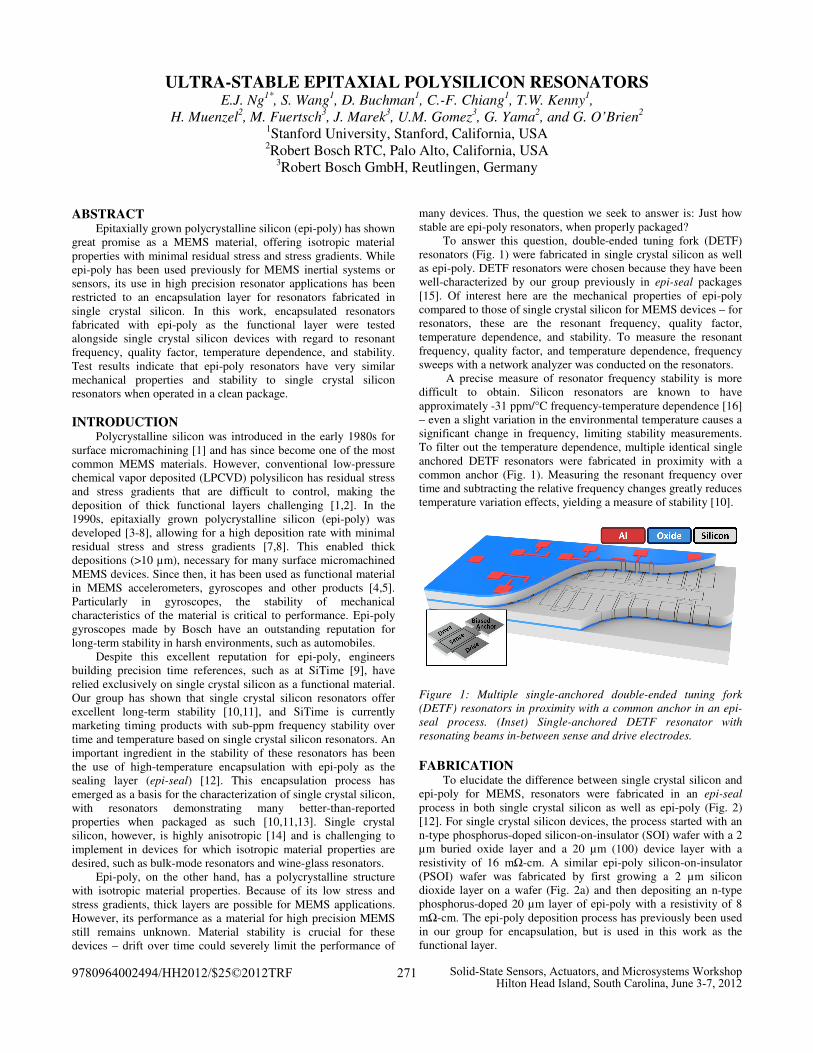
To elucidate the difference between single crystal silicon and epi-poly for MEMS, resonators were fabricated in an epi-seal process in both single crystal silicon as well as epi-poly (Fig. 2) [12]. For single crystal silicon devices, the process started with an n-type phosphorus-doped silicon-on-insulator (SOI) wafer with a 2 µm buried oxide layer and a 20 µm (100) device layer with a resistivity of 16 mΩ-cm. A similar epi-poly silicon-on-insulator (PSOI) wafer was fabricated by first growing a 2 µm silicon dioxide layer on a wafer (Fig. 2a) and then depositing an n-type phosphorus-doped 20 µm layer of epi-poly with a resistivity of 8 mΩ-cm. The epi-poly deposition process has previously been used in our group for encapsulation, but is used in this work as the functional layer.
9780964002494/HH2012/$25©2012TRF 271 Solid-State Sensors, Actuators, and Microsystems WorkshopHilton Head Island, South Carolina, June 3-7, 2012
Epi-poly deposition was performed in an Applied Materials Centura EPI reduced-pressure epitaxial reactor. A thin (approximately 100 nm) seed layer of polysilicon was first deposited using silane (SiH4) in a H2 carrier at 800°C and 600 Torr with a SiH4 gas flow rate of 60 sccm for 90 s. This acts as a nucleation layer for polysilicon deposition on oxide. Dichlorosilane (DCS, SiH2Cl2) at 1080°C and 30 Torr was used to grow 20 µm of polysilicon epitaxially with a flow rate of 400 sccm (DCS) in a H2 carrier. The polysilicon was doped in-situ with 100 sccm of phosphine (PH3). Growth rates were approximately 1 µm/min. Due to chamber limitations, 3 µm of polysilicon was grown at a time, with the wafer kept under load-lock and H2 baked at 1130°C for 300 s between deposition steps to ensure a high quality epitaxial deposition. Chemical Mechanical Polishing (CMP) was then used to planarize the polysilicon wafer surface before further processing.
Following the epi-seal fabrication process as previously detailed [12], identical resonator designs were etched into the
device layer of the SOI and the PSOI wafers using Deep Reactive Ion Etching (DRIE) for a capacitive transduction gap with a trench width of 1.5 µm (Fig. 2b). Tetraethyl orthosilicate (TEOS) oxide was used to refill the trenches and create the oxide spacer between the device layer and the encapsulation (Fig. 2c). Vias were plasma etched in the oxide to allow for electrical access to the electrodes. Thereafter, a first layer of epi-poly (~6 µm) was deposited (Fig. 2d) using the same epi-poly process as described above. Vent holes were etched in this layer using DRIE and the oxide around the device was released with HF vapor (Fig. 2e). A second epi-poly sealing layer (~20 µm) was deposited over the vents to seal the device and to provide mechanical stability (Fig. 2f), with a high temperature (1130°C) H2 bake performed prior to deposition to remove the native oxide around the device. The epitaxial deposition also seals the device cavity under low pressure with H2 remaining in the cavity. For electrical access through the cap to the electrodes, isolation trenches were etched with DRIE. Another layer of oxide was then deposited over the trenches. Finally, aluminum electrical contact pads were patterned (Fig. 2g). To reduce the pressure in the cavity even further, H2 was diffused out by annealing in a nitrogen flow at 400°C for 90 hours.
Single crystal silicon and epi-poly cross-sections are compared in Fig. 3 (a) and (b), with the granular structure of epi-poly clearly noticeable. From another view (Fig. 3c), the epi-poly grains are seen to be columnar and increasing in size from the base (~200 nm) to the top (~5 µm), as also reported in [8]. This occurs as the silicon deposition on top of the nucleation layer continues epitaxially, during which the deposited silicon conforms to the underlying lattice, adding to the existing polycrystalline structure, producing grains that are columnar and growing larger in plane.
(a) (b) (c) Figure 3: (a) Transduction region for single crystal silicon; (b)
Transduction region for epi-poly; (c) Grain structure of epi-poly.
Since the wafers are baked in H2 at high temperatures
(1130°C) and low pressures (30 Torr) during the epitaxial sealing step, silicon migration is expected to occur to minimize surface energy – in single crystal silicon, this has the desirable effect of smoothing out the DRIE scallops. For epi-poly, however, the different crystal orientations result in grain growth along the randomly oriented grains and cause a rough surface with numerous bumps. From SEM images, the surface roughness of the epi-poly is apparent and is about ~0.3 µm. For the resonators tested in this work, the transduction gap size is 1.5 µm and thus no adverse effects from the roughness were observed during resonator testing.
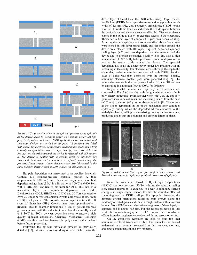
On the completed resonator die (Fig. 4), only the final aluminum electrical traces are visible. The resonators are buried underneath in a vacuum, protected from dust, oxygen, moisture, and other contaminants in the environment.
(a)
(b)
(c)
(d)
(e)
(f)
(g)
Figure 2: Cross-section view of the epi-seal process using epi-poly
as the device layer. (a) Oxide is grown on a handle wafer; (b) Epi-
poly is deposited to form a PSOI (polysilicon on insulator) and
resonator designs are etched in epi-poly; (c) trenches are filled
with oxide; (d) electrical contacts are etched in the oxide and a first
epi-poly encapsulation layer is deposited; (e) vents are etched in
the cap and the oxide around the device is released with HF vapor;
(f) the device is sealed with a second layer of epi-poly; (g)
Electrical isolation and contacts are defined, completing the
process. Single crystal silicon devices were also fabricated in the
same manner starting from an SOI (silicon on insulator) in (b).
272
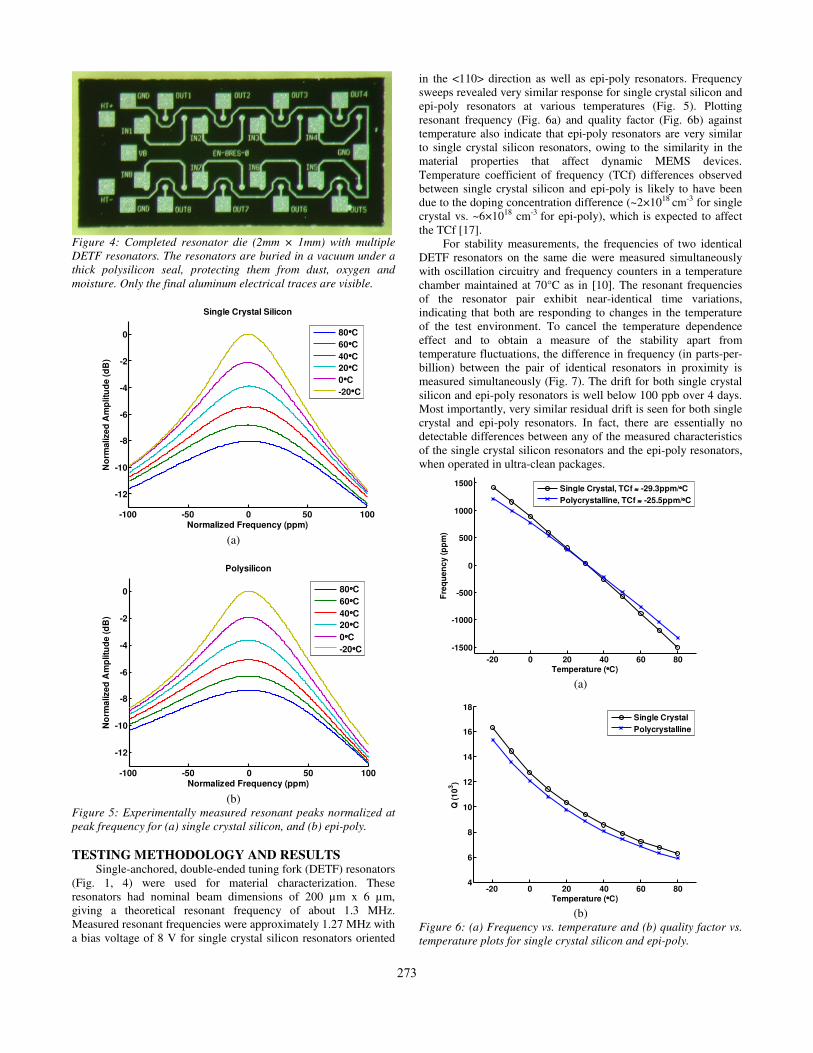
Figure 4: Completed resonator die (2mm × 1mm) with multiple
DETF resonators. The resonators are buried in a vacuum under a
thick polysilicon seal, protecting them from dust, oxygen and
moisture. Only the final aluminum electrical traces are visible.
-100 -50 0 50 100
-12
-10
-8
-6
-4
-2
0
Single Crystal Silicon
No
rmalize
d A
mp
litu
de
(d
B)
Normalized Frequency (ppm)
80°°°°C
60°°°°C
40°°°°C
20°°°°C
0°°°°C
-20°°°°C
(a)
-100 -50 0 50 100
-12
-10
-8
-6
-4
-2
0
Polysilicon
No
rma
lize
d A
mp
litu
de
(d
B)
Normalized Frequency (ppm)
80°°°°C
60°°°°C
40°°°°C
20°°°°C
0°°°°C
-20°°°°C
(b)
Figure 5: Experimentally measured resonant peaks normalized at
peak frequency for (a) single crystal silicon, and (b) epi-poly.
TESTING METHODOLOGY AND RESULTS
Single-anchored, double-ended tuning fork (DETF) resonators (Fig. 1, 4) were used for material characterization. These resonators had nominal beam dimensions of 200 µm x 6 µm, giving a theoretical resonant frequency of about 1.3 MHz. Measured resonant frequencies were approximately 1.27 MHz with a bias voltage of 8 V for single crystal silicon resonators oriented
in the <110> direction as well as epi-poly resonators. Frequency sweeps revealed very similar response for single crystal silicon and epi-poly resonators at various temperatures (Fig. 5). Plotting resonant frequency (Fig. 6a) and quality factor (Fig. 6b) against temperature also indicate that epi-poly resonators are very similar to single crystal silicon resonators, owing to the similarity in the material properties that affect dynamic MEMS devices. Temperature coefficient of frequency (TCf) differences observed between single crystal silicon and epi-poly is likely to have been due to the doping concentration difference (~2×1018 cm-3 for single crystal vs. ~6×1018 cm-3 for epi-poly), which is expected to affect the TCf [17].
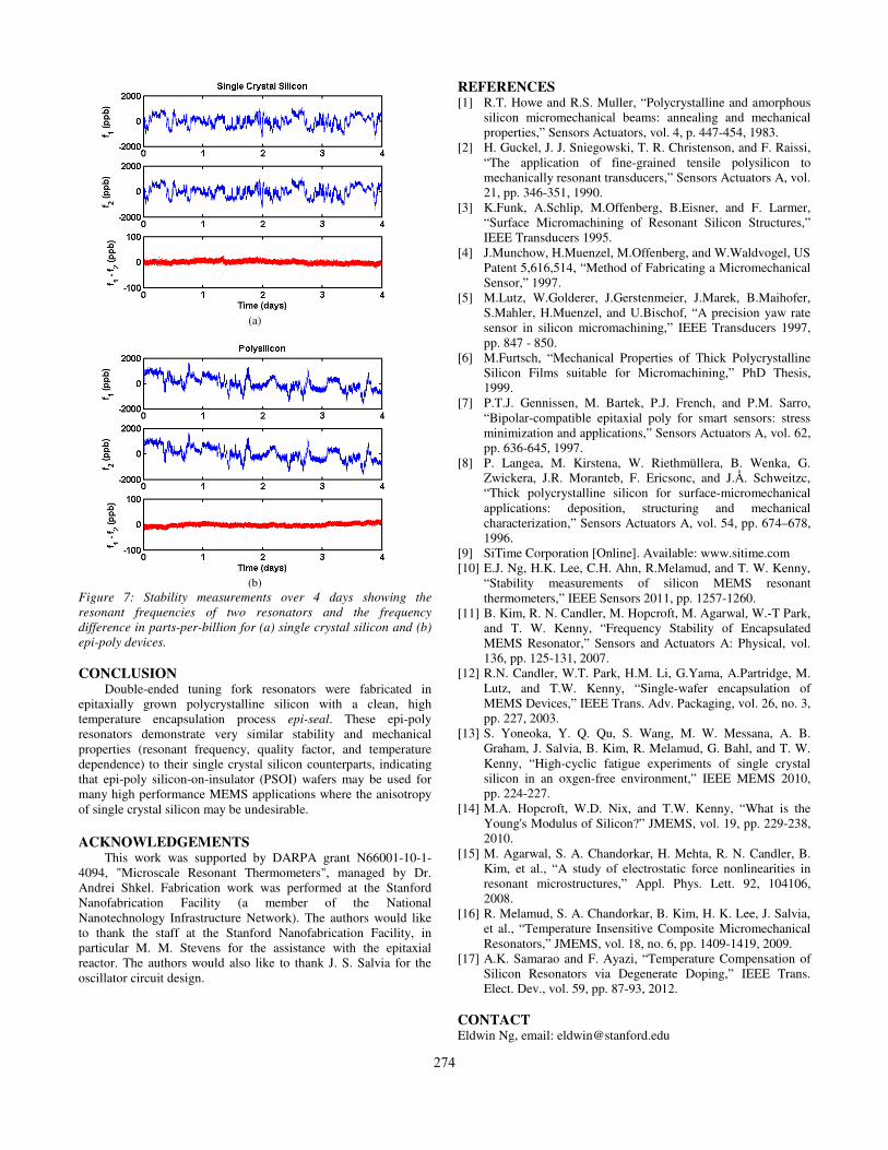
For stability measurements, the frequencies of two identical DETF resonators on the same die were measured simultaneously with oscillation circuitry and frequency counters in a temperature chamber maintained at 70°C as in [10]. The resonant frequencies of the resonator pair exhibit near-identical time variations, indicating that both are responding to changes in the temperature of the test environment. To cancel the temperature dependence effect and to obtain a measure of the stability apart from temperature fluctuations, the difference in frequency (in parts-per-billion) between the pair of identical resonators in proximity is measured simultaneously (Fig. 7). The drift for both single crystal silicon and epi-poly resonators is well below 100 ppb over 4 days. Most importantly, very similar residual drift is seen for both single crystal and epi-poly resonators. In fact, there are essentially no detectable differences between any of the measured characteristics of the single crystal silicon resonators and the epi-poly resonators, when operated in ultra-clean packages.
-20 0 20 40 60 80
-1500
-1000
-500
0
500
1000
1500
Temperature (°°°°C)
Fre
qu
en
cy
(p
pm
)
Single Crystal, TCf ≈≈≈≈ -29.3ppm/°°°°C
Polycrystalline, TCf ≈≈≈≈ -25.5ppm/°°°°C
(a)
-20 0 20 40 60 804
6
8
10
12
14
16
18
Temperature (°°°°C)
Q (
10
3)
Single Crystal
Polycrystalline
(b)
Figure 6: (a) Frequency vs. temperature and (b) quality factor vs.
temperature plots for single crystal silicon and epi-poly.
273
(a)
(b)
Figure 7: Stability measurements over 4 days showing the
resonant frequencies of two resonators and the frequency
difference in parts-per-billion for (a) single crystal silicon and (b)
epi-poly devices.
CONCLUSION
Double-ended tuning fork resonators were fabricated in epitaxially grown polycrystalline silicon with a clean, high temperature encapsulation process epi-seal. These epi-poly resonators demonstrate very similar stability and mechanical properties (resonant frequency, quality factor, and temperature dependence) to their single crystal silicon counterparts, indicating that epi-poly silicon-on-insulator (PSOI) wafers may be used for many high performance MEMS applications where the anisotropy of single crystal silicon may be undesirable.
ACKNOWLEDGEMENTS
This work was supported by DARPA grant N66001-10-1-4094, "Microscale Resonant Thermometers", managed by Dr. Andrei Shkel. Fabrication work was performed at the Stanford Nanofabrication Facility (a member of the National Nanotechnology Infrastructure Network). The authors would like to thank the staff at the Stanford Nanofabrication Facility, in particular M. M. Stevens for the assistance with the epitaxial reactor. The authors would also like to thank J. S. Salvia for the oscillator circuit design.
REFERENCES
[1] R.T. Howe and R.S. Muller, “Polycrystalline and amorphous silicon micromechanical beams: annealing and mechanical properties,” Sensors Actuators, vol. 4, p. 447-454, 1983.
[2] H. Guckel, J. J. Sniegowski, T. R. Christenson, and F. Raissi, “The application of fine-grained tensile polysilicon to mechanically resonant transducers,” Sensors Actuators A, vol. 21, pp. 346-351, 1990.
[3] K.Funk, A.Schlip, M.Offenberg, B.Eisner, and F. Larmer, “Surface Micromachining of Resonant Silicon Structures,” IEEE Transducers 1995.
[4] J.Munchow, H.Muenzel, M.Offenberg, and W.Waldvogel, US Patent 5,616,514, “Method of Fabricating a Micromechanical Sensor,” 1997.
[5] M.Lutz, W.Golderer, J.Gerstenmeier, J.Marek, B.Maihofer, S.Mahler, H.Muenzel, and U.Bischof, “A precision yaw rate sensor in silicon micromachining,” IEEE Transducers 1997, pp. 847 - 850.
[6] M.Furtsch, “Mechanical Properties of Thick Polycrystalline Silicon Films suitable for Micromachining,” PhD Thesis, 1999.
[7] P.T.J. Gennissen, M. Bartek, P.J. French, and P.M. Sarro, “Bipolar-compatible epitaxial poly for smart sensors: stress minimization and applications,” Sensors Actuators A, vol. 62, pp. 636-645, 1997.
[8] P. Langea, M. Kirstena, W. Riethmüllera, B. Wenka, G. Zwickera, J.R. Moranteb, F. Ericsonc, and J.Å. Schweitzc, “Thick polycrystalline silicon for surface-micromechanical applications: deposition, structuring and mechanical characterization,” Sensors Actuators A, vol. 54, pp. 674–678, 1996.
[9] SiTime Corporation [Online]. Available: www.sitime.com [10] E.J. Ng, H.K. Lee, C.H. Ahn, R.Melamud, and T. W. Kenny,
“Stability measurements of silicon MEMS resonant thermometers,” IEEE Sensors 2011, pp. 1257-1260.
[11] B. Kim, R. N. Candler, M. Hopcroft, M. Agarwal, W.-T Park, and T. W. Kenny, “Frequency Stability of Encapsulated MEMS Resonator,” Sensors and Actuators A: Physical, vol. 136, pp. 125-131, 2007.
[12] R.N. Candler, W.T. Park, H.M. Li, G.Yama, A.Partridge, M. Lutz, and T.W. Kenny, “Single-wafer encapsulation of MEMS Devices,” IEEE Trans. Adv. Packaging, vol. 26, no. 3, pp. 227, 2003.
[13] S. Yoneoka, Y. Q. Qu, S. Wang, M. W. Messana, A. B. Graham, J. Salvia, B. Kim, R. Melamud, G. Bahl, and T. W. Kenny, “High-cyclic fatigue experiments of single crystal silicon in an oxgen-free environment,” IEEE MEMS 2010, pp. 224-227.
[14] M.A. Hopcroft, W.D. Nix, and T.W. Kenny, “What is the Young's Modulus of Silicon?” JMEMS, vol. 19, pp. 229-238, 2010.
[15] M. Agarwal, S. A. Chandorkar, H. Mehta, R. N. Candler, B. Kim, et al., “A study of electrostatic force nonlinearities in resonant microstructures,” Appl. Phys. Lett. 92, 104106, 2008.
[16] R. Melamud, S. A. Chandorkar, B. Kim, H. K. Lee, J. Salvia, et al., “Temperature Insensitive Composite Micromechanical Resonators,” JMEMS, vol. 18, no. 6, pp. 1409-1419, 2009.
[17] A.K. Samarao and F. Ayazi, “Temperature Compensation of Silicon Resonators via Degenerate Doping,” IEEE Trans. Elect. Dev., vol. 59, pp. 87-93, 2012.
CONTACT
Eldwin Ng, email: [email protected]
274