Embed Size (px)
Citation preview
1 Ultracompact Silicon-Conductive Oxide Nanocavity Modulator with2 0.02 Lambda-Cubic Active Volume3 Erwen Li,† Qian Gao,† Ray T. Chen,‡ and Alan X. Wang*,†
4†School of Electrical Engineering and Computer Science, Oregon State University, Corvallis, Oregon 97331, United States
5‡Department of Electrical and Computer Engineering, The University of Texas at Austin, Austin, Texas 78758, United States
6 *S Supporting Information
7 ABSTRACT: Silicon photonic modulators rely on the plasma dispersion effect by free-carrier injection or depletion, which can8 only induce moderate refractive index perturbation. Therefore, the size and energy efficiency of silicon photonic modulators are9 ultimately limited as they are also subject to the diffraction limit. Here we report an ultracompact electro-optic modulator with10 total device footprint of 0.6 × 8 μm2 by integrating voltage-switched transparent conductive oxide with one-dimensional silicon11 photonic crystal nanocavity. The active modulation volume is only 0.06 um3, which is less than 2% of the lambda-cubic volume.12 The device operates in the dual mode of cavity resonance and optical absorption by exploiting the refractive index modulation13 from both the conductive oxide and the silicon waveguide induced by the applied gate voltage. Such a metal-free, hybrid silicon-14 conductive oxide nanocavity modulator also demonstrates only 0.5 dB extra optical loss, moderate Q-factor above 1000, and high15 energy efficiency of 46 fJ/bit. The combined results achieved through the holistic design opened a new route for the development16 of next generation electro-optic modulators that can be used for future on-chip optical interconnects.
17 KEYWORDS: Silicon photonics, transparent conductive oxides, optical modulator, photonic crystal cavity, plasmonics
18 The ever-increasing demand to process, store, and exchange19 information creates an unceasing driving force for high-20 bandwidth, energy-efficient photonic technologies. In recent21 years, the vision to develop photonic devices with extremely22 high energy efficiency to attojoule/bit has been outlined.1,2
23 Silicon photonics has the potential to transform future optical24 interconnect systems by reducing the energy consumption and25 enhancing the bandwidth of existing electronic systems by26 orders of magnitude using complementary metal-oxide-semi-27 conductor (CMOS) compatible fabrication processes.3−5 For28 example, silicon electro-optic (E-O) modulators have been29 reported with femtojoule/bit energy efficiency.6,7 In addition to30 the application in optical interconnects, silicon photonic31 devices can also operate the logic gates to conduct certain32 types of optical computation.8−10 However, the performance of33 silicon photonic devices is still limited by the diffraction limit34 and the relatively weak plasma dispersion effect. Although35 silicon has a relatively high refractive index, it can only shrink36 the wavelength inside the silicon waveguide proportionally to37 the scale of λ/n, roughly to 400−600 nm. Further reduction of38 the device footprint requires exploiting surface plasmon39 polaritons (SPPs), which are bound waves at the interface
40between a metal and a dielectric.11 The extremely strong light41confinement of metal−insulator−metal (MIM) waveguide has42led to the demonstration of ultracompact and high-bandwidth43plasmonic E-O modulators.12,13 However, plasmonic structures44and devices are very lossy and can only carry information over a45very short distance. Therefore, hybrid plasmonic-dielectric46waveguide integration must be used for real optical47interconnects,12 which increases the complexity of design and48fabrication.49The second constraint of silicon photonic devices is the50plasma dispersion effect induced by free-carrier injection or51depletion,12 which can only induce moderate refractive index52perturbation. For example, for a typical depletion-based silicon53photonic modulator with a moderate doping level of 2.5 × 10¹⁸
54cm−3 in its active region,6 when it is completely depleted, the55refractive index only changes by 0.06%. As a result, current56Mach−Zehnder interferometer (MZI) silicon modulators57require a long device length up to hundreds of micrometers
Received: October 27, 2017Revised: January 3, 2018Published: January 8, 2018
Letter
pubs.acs.org/NanoLett
© XXXX American Chemical Society A DOI: 10.1021/acs.nanolett.7b04588Nano Lett. XXXX, XXX, XXX−XXX
jml00 | ACSJCA | JCA10.0.1465/W Unicode | research.3f (R3.6.i12 HF03:4459 | 2.0 alpha 39) 2017/11/27 07:41:00 | PROD-JCA1 | rq_11348005 | 1/09/2018 15:58:45 | 7 | JCA-DEFAULT

58 to several millimeters to accumulate sufficient phase modu-59 lation.14 The large device footprint also leads to a large energy60 consumption of picojoule/bit, which cannot meet the require-61 ment of future photonic interconnects application. Compared62 with MZI modulators, resonator-based E-O modulators occupy63 a much smaller footprint and achieve significantly higher energy64 efficiency. To date, various ultracompact silicon microring65 resonators,15−17 microdisks resonators,6,18 and photonic crystal66 nanocavity19 have been demonstrated and used in optical67 interconnect systems, achieving high performance in modu-68 lation speed, compactness, and energy efficiency. However,69 resonator-based modulators have an intrinsic trade-off between70 energy efficiency and optical bandwidth. For practical devices,71 thermal control with integrated heater and temperature sensors72 are often used to obtain stable performance,20,21 but with the73 sacrifice of additional energy consumption and footprint.74 To overcome the intrinsic drawback of the plasma dispersion75 effect of silicon, various functional materials, such as76 graphene,22,23 vanadium oxide,24 and ferroelectric materials25
77 have been integrated with silicon photonics to build next78 generation E-O modulators. Among all these emerging79 materials, transparent conductive oxides (TCOs) have attracted80 escalating interests as a new type of plasmonic material26,27 and81 as active materials for E-O modulators28−31 in recent years due82 to the large tunability of their refractive indices. TCOs, such as83 indium−tin oxide (ITO) and aluminum−zinc oxide (AZO), are84 a family of wide-bandgap semiconductor oxide materials that85 can be degenerately doped to a high level, which is widely used86 in the display industry.32 With free-carrier concentrations87 ranging from 1 × 10¹⁹ to 1 × 1021 cm−3, the real part n of the88 refractive index could experience more than 1 refractive index
f1 89 unit (RIU) change,33 as shown in Figure 1a. Meanwhile, the90 imaginary part κ increases to the same order of magnitude as91 the real part, which causes dramatic increase of the absorption92 30−140× larger than that of silicon, as shown in Figure 1b. In93 recent years, a unique property called epsilon-near-zero (ENZ)94 is verified with TCO materials.34,35 At very high free-carrier
95concentration, the real permittivity of TCOs reaches zero while96the absolute permittivity is a minimum value due to the small97value of the imaginary part as indicated by the vertical dotted98lines in Figure 1c,d. In this case, the electric field will be99strongly confined in TCOs due to the continuity of electric100field displacement at the material interface. ENZ will further101enhance the light−matter interaction as discussed in ref 36. For102silicon, however, it is still far from ENZ even at 1021 cm−3 free-103carrier concentration due to the large value of its high104frequency permittivity.105Existing TCO-based E-O modulators are exclusively based106on straight silicon waveguide28−30 or plasmonic slot wave-107guide31 using electrically induced optical absorption from the108integrated MOS capacitor. The phase change induced by the109real part of the permittivity of the TCO materials, although110automatically accompanying the imaginary part of the index111change, does not contribution to any E-O modulation.112Therefore, a relatively long modulation length (a few microns)113is required to induce sufficient optical absorption. Moreover,114these TCO modulators require the presence of metal gates for115strong plasmonic light confinement and electronic signal116conductance, which introduce relatively high optical loss even117at the transparent state. In this manuscript, we present an118ultracompact hybrid silicon-TCO nanocavity modulator to119overcome the intrinsic drawbacks of those straight waveguide120modulators. There are two exclusive advantages compared with121existing TCO-based modulators. First, the active region of our122plasmonic E-O modulator is free of metal. The metal gate of123the MOS capacitor is replaced by an ITO gate, which induces124much smaller optical absorption compared with other metal-125gated modulators. This ITO−oxide−Si capacitor offers the126possibility to build a relatively high Q-factor resonator while127traditional metal−oxide−ITO cannot. Second, in our nano-128cavity E-O modulator, both the phase change and the129absorption, from both the Si and ITO materials, will contribute130coherently to E-O modulation. The total device footprint of our131TCO modulator is only 0.6 × 8 μm2 using one-dimensional132(1D) photonic crystal (PC) nanocavity with 20 nm SiO2 as the133insulator and 20 nm ITO as the gate. The E-O modulation134volume is less than 0.06 μm3 (width × height × length = 0.56135μm × 0.28 μm × 0.375 μm), namely, only 2% of lambda-cubic136(0.02λ3) volume, which is the smallest active modulation region137that has ever been reported to the best of our knowledge. The138E-O modulation volume is the most critical device metric that139affects the energy efficiency of an E-O modulator,1 which is140usually achieved by compact resonant cavities or plasmonic141structures. A few ultracompact resonator-based E-O modulators142have been reported, including microdisk modulators6,18 using143vertical p−n junction with an active volume of 1.6−2.5 μm3 and144p−i−n photonic crystal nanocavity modulator19 with a145modulation volume of 2.2 μm3. Non-resonator-type TCO146plasmonic modulators have typical lengths of 5 μm30 to 10147μm31 long, with calculated active modulation volume around1480.6 μm3. Our device combines the advantages of ultracompact149resonators and TCO plasmonics, which further reduces the150active E-O modulation volume by 10×.151Briefly, the applied gate voltage induces free electron and152hole accumulation ITO and silicon, respectively. The free-153carrier-induced variation of the real part of the optical154permittivity causes blue-shift of the resonance peak, while the155increase of the imaginary part of the optical permittivity induces156optical absorption of the resonance mode, which becomes157more prominent when ITO is close to ENZ. We experimentally
Figure 1. (a) Real part (n) and (b) imaginary part (κ) of the refractiveindices of p-type Si (green solid) and ITO (orange solid) as a functionof free-carrier concentration Nc (hole in Si, Nh,Si; and electron in ITO,Ne,ITO) at wavelength λ = 1.55 μm. (See the Supporting Informationfor calculation details.) (c) Real part (ε1) and (d) imaginary part (ε2)of the relative permittivity of p-type Si (green solid line) and ITO(orange solid line) as a function of Nc at wavelength λ = 1.55 μm. Theorange dashed line in part c shows the absolute permittivity of ITO(|εr,ITO|), and the pink dashed line indicates the Nc where the ITOreaches ENZ.
Nano Letters Letter
DOI: 10.1021/acs.nanolett.7b04588Nano Lett. XXXX, XXX, XXX−XXX
B

158 achieved a large E-O response of 30 pm/V and high energy159 efficiency of 46 fJ/bit. Compared with those of reported TCO-160 based plasmonic modulators, the active region of our device is
161completely free of metallic materials, which offers a low device162loss of only 0.5 dB, moderately high Q-factor of 1000, and163better compatibility with CMOS processes. Compared with the
Figure 2. (a) 3D schematic of the Si-ITO modulator. (b) Colored scanning electron micrograph (SEM) of the fabricated Si-ITO modulator. Theinsertion figure shows the zoomed-in view of the center of the MOS capacitor region. (c) Optical image of the fabricated modulator.
Figure 3. (a) Cross-section of the Si/oxide/ITO MOS capacitor at the center of the hybrid Si-ITO modulator. When a negative bias is applied onthe ITO gate, electrons and holes accumulate at the ITO/oxide and Si/oxide interfaces, respectively. (b) Electrical potential distribution in ITO(blue lines) and Si (red lines) as a function of electrical displacement field in the gate oxide layer, Dox. (c) Carrier density distribution in ITO(electron) and Si (hole) as a function of Dox field. (d) The real part refractive index (n) distribution in ITO and Si as a function of Dox field. (e) Gatevoltage as a function of the Dox field for different gate oxide layers: 20 nm SiO2 (red line), 5 nm SiO2 (blue line), 5 nm Al2O3 (yellow line), and 5 nmHfO2 (green line). The dashed lines show the Dox field range when the gate oxide layer will breakdown. The shaded area enclosed by the purpledashed line shows the Dox field range when the permittivity of ITO accumulation layer, |εr,ITO|, is smaller than 1, representing the ENZ region; thepurple solid line indicates the Dox field when |εr,ITO| reaches minimum ENZ value.
Nano Letters Letter
DOI: 10.1021/acs.nanolett.7b04588Nano Lett. XXXX, XXX, XXX−XXX
C
164 conventional silicon ring resonator or microdisk modulator, our165 device shows exclusive advantages as it provides a larger166 resonant wavelength tuning and much higher usable optical167 bandwidth of greater than 1 nm. Through future research by168 replacing the current SiO2 gate with high-k materials and169 improving the Q-factor, we can potentially achieve even higher170 energy efficiency below 1 fJ/bit.171 The schematic of the ITO-gated 1D silicon PC nanocavity is
f2 172 shown in Figure 2a. The device consists of a MOS capacitor173 built at the center of the nanocavity on a silicon strip174 waveguide. The strip waveguide is fabricated on a p-type175 silicon-on-insulator (SOI) substrate with 500 nm in width and176 250 nm in height. A pair of grating couplers are integrated to177 couple light in and out of an optical fiber. The PC cavity is178 defined through electron beam lithography (EBL) and reactive179 ion etching (RIE), operating in the TE mode. Two photonic180 crystal mirror segments are placed back-to-back adjacent to the181 nanocavity. The air hole size is quadratically tapered down from182 the center of the cavity region to the edge of the two mirror183 segments. In our design, each mirror segment has 12 air holes.184 The filling factor, which is defined as f = A/pw, is tapered down185 from 0.23 in the center to 0.1 at the edge, where A is the air186 hole area, p is the air hole period, and w is the waveguide width.187 The period p is chosen to be 340 nm to allow the modulator to188 operate in the telecommunications wavelength range. In the189 center of the cavity, an ITO/SiO2/Si film stack creates a MOS
f3 190 capacitor with cross-sectional view shown in Figure 3a. Here,191 the silicon waveguide also serves as the bottom electrode192 despite its relatively high resistivity. Two 400 nm wide silicon193 strips are used to form the conduction path between the silicon194 waveguide and the silicon slab with the contact electrodes.195 Then, a 20 nm thick SiO2 layer is thermally grown on top of the196 entire silicon PC nanocavity serving as the gate oxide. Finally, a197 20 nm thick ITO layer is sputtered, performing as the metallic198 gate electrode. We need to emphasize that the center199 nanocavity length is only 120 nm, which is at least 50× shorter200 than ring resonators or microdisk resonators. A 375 nm long201 ITO gate is made to compensate the misalignment of the202 electron beam lithography (EBL) process as shown by the inset203 figure of Figure 2b. The SEM and optical images of one204 fabricated device are depicted in Figure 2b,c (see the205 Supporting Information for details of fabrication).206 The device operates in the accumulation mode of the MOS207 capacitor with the negative gate bias on the ITO gate. Unlike208 other reported TCO-MOS E-O modulators which ignore the209 free-carrier effect in the metal gate, we consider the free-carrier210 accumulation at both sides of the interfaces, i.e., in the ITO/211 SiO2 and Si/SiO2 interfaces. We perform a numerical212 simulation systematically to analyze the carrier distribution in213 the accumulation layers versus the applied gate bias. In our214 modeling, the carrier density and electric potential in the ITO215 and Si regions are treated in different ways. The main difference216 is that the high doping level of ITO results in an initial Fermi217 level higher than the bottom of the conduction band.218 Therefore, the electron density and electric potential in ITO219 behave more like a metal, which can be approximated by the220 Thomas−Fermi screening model.37,38 On the other side, Si221 follows the classic semiconductor theory.39 However, a large222 band bending is expected in our device, and a traditional223 Boltzmann distribution approximation is not accurate. A224 rigorous analysis using the Fermi−Dirac distribution is used225 to model the Si side. In order to obtain representative results,226 we conduct our modeling using the electric displacement field
227Dox instead of the electric field E. The boundary condition only228requires the value of Dox in the gate oxide layer, making the229modeling independent of the gate oxide material and thickness.230We plot the electric potential and carrier distribution as a231function of Dox as shown in Figure 3b,c. We can see that the232electron concentration in ITO (Ne,ITO) accumulates from 1 ×2331020 to 7.46 × 1020 cm3, and the hole concentration in Si (Nh,Si)234accumulates from 1 × 10¹⁷ to 1.08 × 1021 cm3 with a Dox/ε0235value of 78 MV/cm. Surprisingly, the peak of Nh,Si is even236higher than that of Ne,ITO, which is because of the larger237effective density of state of Si compared with that of ITO (see238the Supporting Information). As a result, Nh,Si in Si is more239sensitive to electrical potential modulation than Ne,ITO in ITO.240The ITO reaches the ENZ region when the Ne,ITO is 6.4 × 10²⁰
241cm3 with Dox/ε0 of 67 MV/cm. Figure 3d plots the242corresponding distribution of the refractive indices of ITO243and Si. Both ITO and Si exhibit dramatic refractive index244modulation within a thin layer of ∼1 nm thick close to the245interface even at a relatively small Dox field. For the ITO side,246the effect of this thin accumulation layer is already well-247recognized.30,37,38 This layer is often treated as an effective248accumulation layer, and the thickness can be estimated by the249Thomas−Fermi screening length, Ltf. On the Si side, this thin250accumulation layer could also play a critical role for the E-O251modulation but was not utilized by simple straight waveguides252in published papers. Detailed analysis will be provided in the253following section. Next, knowing the Dox field, we can calculate
254the gate voltage by |= |Ψ + + |Ψ |
ε εV D t
gate ITO Siox ox
0 oxide,st, where ΨITO
255and ΨSi are the surface potential at the ITO/SiO2 and the Si/256SiO2 interface, ε0 is the vacuum permittivity, and εoxide,st and tox257are the static relative permittivity and thickness of the gate258oxide layer. Figure 3e plots the applied gate voltage as a259function of Dox field with different oxide materials and260thicknesses. Here the dashed lines indicate a large Dox field261exceeding the breakdown of the gate oxide. From this analysis,262it is obvious to draw a conclusion that thinner oxide layer263thickness and high-k materials will help to reduce the applied264bias voltage. Besides, to truly reach the ENZ operation of the265ITO layer, a high-k gate material such as HfO2 is necessary. In266our experimental demonstration, we chose SiO2 as the gate267oxide material primarily due to our current fabrication facilities.268The Si-ITO nanocavity modulator operates in the dual mode269of cavity resonance and optical absorption. At a relatively small270applied bias, the device operates in the “normal mode”, when271the Ne,ITO is not high enough to push ITO into the ENZ272confinement. Modulation of the nanocavity resonance domi-273nates, which mainly comes from the real parts of the274permittivity change (Δε1) induced by the plasma dispersion275effect of the ITO and Si. Based on the cavity perturbation276theory, the resonance shift (Δω) can be expressed as40
∫∫
ωε
εΔ =
− Δ *
*
ω E E v
E E v
d
d2
277where ω is the original resonance frequency, ε and Δε are the278distribution of the original and changed permittivity, and E is279the electric field distribution of the cavity mode. We know that280the permittivity change caused by the plasma dispersion is281proportional to the change of free-carrier concentration,282namely, Δε ∝ ΔNc. This means that the resonance shift283induced by a 1 nm thick accumulation layer with a Nc of 1 ×2841020 cm−3 is equivalent to the shift induced by a 100 nm thick
Nano Letters Letter
DOI: 10.1021/acs.nanolett.7b04588Nano Lett. XXXX, XXX, XXX−XXX
D
285 layer from full depletion to a Nc of 1 × 1018 cm−3 under thef4 286 uniform optical field distribution approximation. Figure 4a,b
287 shows the simulated photonic crystal cavity mode profile. The288 cavity mode has a good overlap with the accumulation layer of289 the MOS structure near the center air holes and is relatively290 uniform. Thus, it is reasonable to assume an approximately291 uniform optical distribution here. The resonance shift has the292 following relationship:
∫ω
ω
εωε
ωε
ωε γ
Δ ∝Δ
= Δ = = ∝N v
vQv
CVv
CVv
Cv
dc
eff c eff c eff c eff a a
293 where εeff and vc are the effective permittivity and mode volume294 of the cavity mode, ΔQ is the accumulated free carriers induced295 by the applied voltage V, C and va are the capacitance and296 volume of the active modulation region of the modulator,297 respectively, and γ is the coefficient describing the overlapping298 between va and vc. Additionally, due to the small mode volume299 of the photonic crystal cavity mode and its large overlap with300 the active modulation region of the modulator (Figure 4b), we301 can conclude that the resonance shift is proportional to the302 capacitance per unit active volume. Large capacitance C and303 small active volume va are preferred for high modulation304 efficiency. Since we effectively construct a 3D MOS capacitor in305 the center of the photonic crystal cavity, free carriers306 accumulate at all three interfaces. As large C/va ratio is realized,307 we can achieve significant resonance modulation within 0.02λ3
308 active modulation volume. In spite of the resonance shift309 induced by the real part permittivity change, the optical310 absorption from the imaginary part change of the permittivity,311 which is usually a minor effect in pure silicon modulators, also
312plays an important role in the Si-ITO hybrid modulator313because of the 30−140× larger imaginary part of ITO314compared with Si. As a result, larger extinction ratio can be315achieved at the same resonance tuning. As the applied bias316increases, the accumulation layer of ITO approaches the ENZ317region as shown by the shaded area in Figure 3e. Once the318modulator reaches the “ENZ mode”, the optical mode starts to319be confined in the ITO accumulation layer. This ENZ320confinement effect is highly polarization sensitive. For our321photonic crystal nanocavity design operating in the TE mode, it322mainly happens at the sidewall interface as shown in Figure 4b.323The ENZ confinement effect will dramatically enhance the
324absorption which is proportional to
εε| |22,ITO
ITO2 .41 In this case, the
325optical absorption mode dominates. Figure 4c plots the326simulated transmission spectra of the hybrid Si-ITO modulator327at different carrier concentrations in the accumulation region,328Ne,ITO,acc. The black dashed line outlines the evolution of the329transmission peak. The trend from the normal resonance330modulation to ENZ electroabsorption is clearly shown as Ne,ITO
331increases.332The E-O modulation response of fabricated hybrid Si-ITO333modulator was characterized (see the Supporting Information334for details of measurement setup). Figure 4d shows the335measured transmission spectra as a function of the applied bias.336The spectra are normalized to a straight Si waveguide as the337reference. The insertion loss (IL) of the PC nanocavity338modulator is only 0.5 dB at the peak resonance wavelength.339The free-carrier concentration of as-sputtered ITO is 1 × 10²⁰
340cm−3, which is still a dielectric material at telecommunications341wavelengths. The measured Q-factor after ITO deposition is
Figure 4. (a) Photonic crystal cavity mode profiles of “normal mode” (accumulation layer Ne,ITO = 1 × 1020 cm−3) and “ENZ mode” (accumulationlayer Ne,ITO = 6.4 × 1020 cm−3). The optical field intensity is plotted in log scale. Clearly, at “ENZ mode” the transmission drops due to the ITOabsorption. (b) Zoomed-in mode profile of “normal mode” and “ENZ mode”. The optical intensity is plotted in normalized linear scale. Inset:further zoomed-in mode profile of “ENZ mode” at the ITO/SiO2 interface. It is clearly shown that in “ENZ mode” the optical field is stronglyconfined in the accumulation layer at the side wall. (c) Simulated normalized transmission spectrum at different free-carrier concentration Ne,ITO,acc inthe ITO accumulation region. The black dashed line outlines the change of the transmission peak as Ne,ITO increases. (d) Measured statictransmission spectrum as a function of the applied bias voltage. The DC applied bias ranges from 0 to 19.5 V. (e) Measured extinction ratio (ER)spectrum as a function of the applied bias voltage.
Nano Letters Letter
DOI: 10.1021/acs.nanolett.7b04588Nano Lett. XXXX, XXX, XXX−XXX
E
342 around 1000, which is slightly smaller than the Q-factor343 measured before sputtering the ITO (∼1200), proving that the344 degradation of the Q-factor due to the thin ITO layer is minor.345 The resonance wavelength blue-shifts by 0.57 nm with a change346 in DC bias from 0 to −19.5 V, indicating a 30 pm/V347 modulation efficiency. Meanwhile, we observe a significant drop348 of the peak transmission by 45.34%, which is caused by the349 resonance shift as well as the optical absorption. The MOS350 capacitor operation is verified by the low leakage current, which351 is measured to be less than 100 fA at −20 V. Figure 4e plots the352 extinction ratio (ER) spectrum as a function of the applied bias.353 A usable optical bandwidth of greater than 1 nm is observed if354 we allow 1 dB variation of the ER. The maximum modulation is355 observed at 1533.78 nm, which introduces an additional loss of356 0.75 dB as compared to the peak wavelength. The transmission357 varies by 5.6 dB with a bias changing from 0 to −19.5 V. The358 dynamic modulation speed is demonstrated up to 3.2 MHz
f5 359 with an AC voltage swing of 0 to −12 V (as shown in Figure 5),360 which is limited by our testing instruments.
361 Here we estimated the modulation speed and energy362 efficiency of the hybrid Si-ITO nanocavity modulator. The363 speed of the modulator is limited by the RC delay since its364 operation is based on the fast accumulation mode of a MOS365 capacitor. The finite element method (FEM) simulation gives366 the capacitance of the modulator including the whole PC367 nanocavity and the ITO gate in the active region to be 1.28 fF.368 The series resistance of our fabricated device is around 4.9 MΩ,369 which is limited by the lightly doped (1 × 1015 cm−3) SOI slab.370 Consequently, our current device has a relatively slow RC-371 limited speed of 160 MHz. However, the series resistance can372 be reduced to ∼9 KΩ by selectively doping the silicon373 conduction strips and PC waveguide to a high level of 5 × 10¹⁸
374 cm−3 while keeping the doping of the center active cavity375 region at a moderate high level of 1 × 1017 cm−3 (see the376 Supporting Information for details of capacitance and resistance377 calculation). The optical loss of a passive silicon waveguide with378 high-level doping is around 0.017 dB/μm according to our379 optical FEM simulation. A 10 μm long silicon waveguide with380 high doping level will only introduce an additional loss of 0.17381 dB. Besides, the corresponding silicon waveguide loss of382 moderate high doping level is 3.4 × 10⁻⁴ dB/μm. For a cavity383 with a moderate Q-factor of 5000, which corresponds to a384 photon lifetime of 4.2 ps, the increasing in optical loss is only
3850.12 dB. As a result, the RC-limited bandwidth can be386improved to 87 GHz. However, the real achievable operation387speed will be limited by the electronic circuit or signal388generator. The energy efficiency of the modulator is estimated389using Eper‑bit = CV2/4. Assuming a 12 V voltage swing (3 dB ER390at the resonance peak), the energy consumption of the device is391only 46 fJ/bit. Since the free-carrier accumulation in the MOS392only depends on the D field in the gate insulator, the393performance of the hybrid silicon-ITO modulator can be394further improved with high-k materials such as HfO2. For395example, if we replace the 20 nm SiO2 with 5 nm thick HfO2,396the applied voltage will be reduced to 1 V to achieve the same397D field using current 12 V bias. In this case, the RC-limited398speed will decrease to 40 GHz due to the increased capacitance.399However, the resonance tuning efficiency will increase to 360400pm/V, and the energy consumption will drop to 6.2 fJ/bit. In401addition, our current hybrid silicon-ITO nanocavity modulator402only possesses a moderate Q-factor of 1000 due to our403fabrication quality such as the surface roughness and the404deviation of the air hole diameters. Through advanced405designs42 and optimized fabrication, a PC nanocavity with406higher Q-factor is achievable. We anticipate that both the ER407and the operation voltage will be improved in further408development, offering the possibility to achieve hundreds of409attojoule/bit energy efficiency in the future. For example, if the410Q-factor is improved to 5000 (Q-factor-limited bandwidth will411be 240 GHz), we can further reduce the operational voltage by4125× and improve the energy efficiency by 25× to 250 aJ/bit.
413■ ASSOCIATED CONTENT414*S Supporting Information415The Supporting Information is available free of charge on the416ACS Publications website at DOI: 10.1021/acs.nano-417lett.7b04588.
418Calculation of permittivity and refractive index of ITO419and Si, details of electrical modeling of ITO/oxide/Si420capacitor, optical simulation, calculation of the capaci-421tance and resistance, experimental details of device422fabrication, and measurement setup (PDF)
423■ AUTHOR INFORMATION424Corresponding Author425*E-mail: [email protected] X. Wang: 0000-0002-0553-498X428Author Contributions429A.X.W. and R.T.C. conceived the ideas of the project. E.L.430performed the simulations and devised the geometry of the431modulators. E.L. and Q.G. fabricated the hybrid Si-ITO432modulators. E.L. conducted the optical and electrical character-433ization of the modulators under the supervision of A.X.W. All434authors discussed the results. E.L. and A.X.W. cowrote the435paper. R.T.C. and A.X.W. supervised the project.436Notes437The authors declare no competing financial interest.
438■ ACKNOWLEDGMENTS439The authors thank Spencer Liverman for his simulation of the440device capacitance using FEM and Prof. John F. Wager for the441discussion of MOS modeling and the help of ITO sputtering442from his group. Simulations have been carried out on the
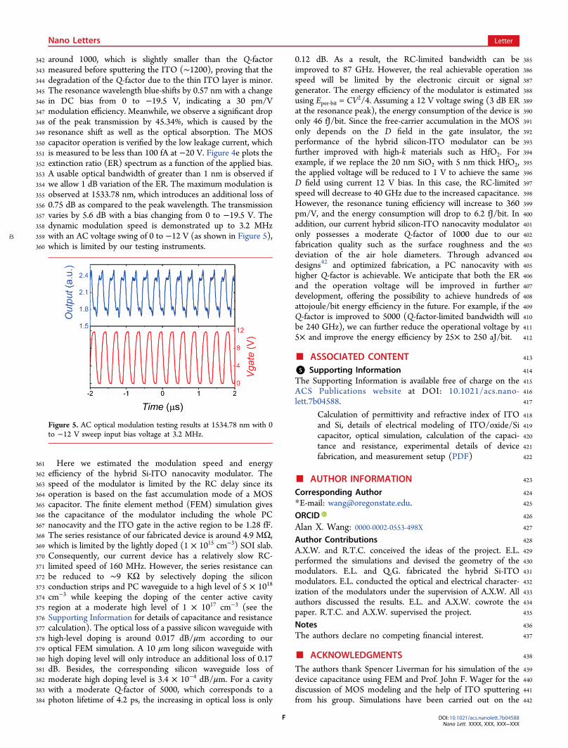
Figure 5. AC optical modulation testing results at 1534.78 nm with 0to −12 V sweep input bias voltage at 3.2 MHz.
Nano Letters Letter
DOI: 10.1021/acs.nanolett.7b04588Nano Lett. XXXX, XXX, XXX−XXX
F
443 workstations of Prof. Ray T. Chen’s group at the University of444 Texas at Austin. This work is supported by the AFOSR MURI445 Project FA9550-17-1-0071 under the guidance of Dr. Gernot446 Pomrenke.
447 ■ REFERENCES(1)448 Miller, D. A. J. Lightwave Technol. 2017, 35, 346−396.(2)449 Pan, Z.; Zhang, C.; Subbaraman, H.; Chung, C. J.; Li, Q.; Xu, X.;
450 Zhang, X.; Guo, L. J.; Chen, R. T. In SPIE OPTO, February, 2017;451 International Society for Optics and Photonics.
(3)452 Soref, R. IEEE J. Sel. Top. Quantum Electron. 2006, 12, 1678−453 1687.
(4)454 Asghari, M.; Krishnamoorthy, A. V. Nat. Photonics 2011, 5, 268−455 270.
(5)456 Rumley, S.; Nikolova, D.; Hendry, R.; Li, Q.; Calhoun, D.;457 Bergman, K. J. Lightwave Technol. 2015, 33, 547−562.
(6)458 Timurdogan, E.; Sorace-Agaskar, C. M.; Sun, J.; Hosseini, E. S.;459 Biberman, A.; Watts, M. R. Nat. Commun. 2014, 5, 5008.
(7)460 Leuthold, J.; Koos, C.; Freude, W. Nat. Photonics 2010, 4, 535−461 544.
(8)462 Tian, Y.; Zhang, L.; Ji, R.; Yang, L.; Zhou, P.; Chen, H.; Ding, J.;463 Zhu, W.; Lu, Y.; Jia, L.; Fang, Q. Opt. Lett. 2011, 36, 1650−1652.
(9)464 Xu, Q.; Soref, R. Opt. Express 2011, 19, 5244−5259.(10)465 Wang, Z.; Ying, Z.; Dhar, S.; Zhao, Z.; Pan, D. Z.; Chen, R. T. In
466 CLEO: Science and Innovations, May, 2017; Optical Society of America.(11)467 Barnes, W. L.; Dereux, A.; Ebbesen, T. W. Nature 2003, 424,
468 824.(12)469 Melikyan, A.; Alloatti, L.; Muslija, A.; Hillerkuss, D.; Schindler,
470 P. C.; Li, J.; Palmer, R.; Korn, D.; Muehlbrandt, S.; Van Thourhout,471 D.; Chen, B. Nat. Photonics 2014, 8, 229−233.
(13)472 Haffner, C.; Heni, W.; Fedoryshyn, Y.; Niegemann, J.; Melikyan,473 A.; Elder, D. L.; Baeuerle, B.; Salamin, Y.; Josten, A.; Koch, U.;474 Hoessbacher, C. Nat. Photonics 2015, 9, 525−528.
(14)475 Watts, M. R.; Zortman, W. A.; Trotter, D. C.; Young, R. W.;476 Lentine, A. L. Opt. Express 2011, 19, 21989−22003.
(15)477 Tanabe, T.; Nishiguchi, K.; Kuramochi, E.; Notomi, M. Opt.478 Express 2009, 17, 22505−22513.
(16)479 Soref, R. A.; Bennett, B. R. IEEE J. Quantum Electron. 1987, 23,480 123−129.
(17)481 Ding, J.; Chen, H.; Yang, L.; Zhang, L.; Ji, R.; Tian, Y.; Zhu, W.;482 Lu, Y.; Zhou, P.; Min, R.; Yu, M. Opt. Express 2012, 20, 7081−7087.
(18)483 Xu, Q.; Schmidt, B.; Pradhan, S.; Lipson, M. Nature 2005, 435,484 325.
(19)485 Xiao, X.; Li, X.; Xu, H.; Hu, Y.; Xiong, K.; Li, Z.; Chu, T.; Yu, J.;486 Yu, Y. IEEE Photonics Technol. Lett. 2012, 24, 1712−1714.
(20)487 Reed, G. T.; Mashanovich, G.; Gardes, F. Y.; Thomson, D. J.488 Nat. Photonics 2010, 4, 518−526.
(21)489 DeRose, C. T.; Watts, M. R.; Trotter, D. C.; Luck, D. L.;490 Nielson, G. N.; Young, R. W. In Conference on Lasers and Electro-optics,491 May, 2010; Optical Society of America.
(22)492 Liu, M.; Yin, X.; Ulin-Avila, E.; Geng, B.; Zentgraf, T.; Ju, L.;493 Wang, F.; Zhang, X. Nature 2011, 474, 64.
(23)494 Youngblood, N.; Anugrah, Y.; Ma, R.; Koester, S. J.; Li, M. Nano495 Lett. 2014, 14, 2741−2746.
(24)496 Briggs, R. M.; Pryce, I. M.; Atwater, H. A. Opt. Express 2010, 18,497 11192−11201.
(25)498 Xiong, C.; Pernice, W. H.; Ngai, J. H.; Reiner, J. W.; Kumah, D.;499 Walker, F. J.; Ahn, C. H.; Tang, H. X. Nano Lett. 2014, 14, 1419−500 1425.
(26)501 Naik, G. V.; Kim, J.; Boltasseva, A. Opt. Mater. Express 2011, 1,502 1090−1099.
(27)503 Naik, G. V.; Shalaev, V. M.; Boltasseva, A. Adv. Mater. 2013, 25,504 3264−3294.
(28)505 Ma, Z.; Li, Z.; Liu, K.; Ye, C.; Sorger, V. J. Nanophotonics 2015,506 4, 198−213.
(29)507 Keeler, G. A.; Geib, K. M.; Serkland, D. K.; Parameswaran, S.;508 Luk, T. S.; Grine, A. J.; Ihlefeld, J.; Campione, S.; Wendt, J. R. In
509Optical Fiber Communication Conference, March, 2017; Optical Society510of America.
(30) 511Sorger, V. J.; Lanzillotti-Kimura, N. D.; Ma, R. M.; Zhang, X.512Nanophotonics 2012, 1, 17−22.
(31) 513Lee, H. W.; Papadakis, G.; Burgos, S. P.; Chander, K.; Kriesch,514A.; Pala, R. A.; Peschel, U.; Atwater, H. A. Nano Lett. 2014, 14, 6463−5156468.
(32) 516Chiang, H. Q.; Wager, J. F.; Hoffman, R. L.; Jeong, J.; Keszler,517D. A. Appl. Phys. Lett. 2005, 86, 013503.
(33) 518Feigenbaum, E.; Diest, K.; Atwater, H. A. Nano Lett. 2010, 10,5192111−2116.
(34) 520Vasudev, A. P.; Kang, J. H.; Park, J.; Liu, X.; Brongersma, M. L.521Opt. Express 2013, 21, 26387−26397.
(35) 522Park, J.; Kang, J. H.; Liu, X.; Brongersma, M. L. Sci. Rep. 2015, 5,52315754.
(36) 524Liberal, I.; Engheta, N. Nat. Photonics 2017, 11, 149−158.(37) 525Melikyan, A.; Lindenmann, N.; Walheim, S.; Leufke, P. M.;
526Ulrich, S.; Ye, J.; Vincze, P.; Hahn, H.; Schimmel, T.; Koos, C.;527Freude, W. Opt. Express 2011, 19, 8855−8869.
(38) 528Krasavin, A. V.; Zayats, A. V. Phys. Rev. Lett. 2012, 109, 053901.(39) 529Colinge, J. P.; Colinge, C. A. Physics of semiconductor devices;
530Springer Science & Business Media, 2005.(40) 531Meng, B.; Booske, J.; Cooper, R. IEEE Trans. Microwave Theory
532Tech. 1995, 43, 2633−2636.(41) 533Shi, K.; Lu, Z. Opt. Commun. 2016, 370, 22−28.(42) 534Md Zain, A. R.; Johnson, N. P.; Sorel, M.; Richard, M. Opt.
535Express 2008, 16, 12084−12089.
Nano Letters Letter
DOI: 10.1021/acs.nanolett.7b04588Nano Lett. XXXX, XXX, XXX−XXX
G