Embed Size (px)
Citation preview
Ultrafast carrier dynamics of epitaxial silicene Eugenio Cinquanta,1,† Guido Fratesi,2,3 Stefano dal Conte,4,5 Carlo Grazianetti,1 Francesco
Scotognella,5,* Salvatore Stagira,5 Caterina Vozzi,4 Giovanni Onida,2,3 and Alessandro Molle1,*
1Laboratorio MDM, IMM-CNR, via C. Olivetti 2, Agrate Brianza, I-20864, Italy 2Dipartimento di Fisica, Universita` degli Studi di Milano, Via Celoria 16, 20133 Milano, Italy
3European Theoretical Spectroscopy Facility, Via Celoria 16, 20133 Milano, Italy 4CNR Istituto di Fotonica e Nanoteconologie, Piazza Leonardo da Vinci 32, 20133 Milano, Italy
5Dipartimento di Fisica, Politecnico di Milano, Piazza L. da Vinci 32, 20133 Milano, Italy *[email protected] phone +39 039 603 2884 fax + 39 039 688 1175 *[email protected]; phone +39 02 2399 6056; fax +39 02 2399 6126
* [email protected]; phone +39 02 503 17348; fax +39 02 503 17482 † present address Dipartimento di Fisica, Politecnico di Milano, Piazza L. da Vinci 32, 20133 Milano, Italy
Abstract
The recent integration of silicene in field-effect transistors (FET) opened new challenges in the comprehension of the chemical and physical properties of this elusive two-dimensional allotropic form of silicon. Intense efforts have been devoted to the study of the epitaxial Silicene/Ag(111) system in order to elucidate the presence of Dirac fermion in analogy with graphene; strong hybridization effects in silicene superstructures on silver have been invoked as responsible for the disruption of π and π* bands. In this framework, the measured ambipolar effect in silicene-based FET characterized by a relatively high mobility, points out to a complex physics at the silicene-silver interface, demanding for a deeper comprehension of its details on the atomic scale. Here we elucidate the role of the metallic support in determining the physical properties of the Si/Ag interface, by means of optical techniques combined with theoretical calculations of the optical response of the supported system. The silicene/Ag(111) spectra, which turn out to be strongly non-additive, are analyzed in the framework of theoretical density functional based calculations allowing us to single out contributions arising from different localization. Electronic transitions involving silver states are found to provide a huge contribution to the optical absorption of silicene on silver, compatible with a strong Si-Ag hybridization. The results point to a dimensionality-driven peculiar dielectric response of the two-dimensional-silicon/silver interface, which is confirmed by means of Transient-Reflectance spectroscopy. The latter shows a metallic-like carrier dynamics, (both for silicene and amorphous silicon), hence providing an optical demonstration of the strong hybridization arising in silicene/Ag(111) systems.
Keywords: two-dimensional materials; silicene; ultrafast spectroscopy.
1. INTRODUCTION A very interesting system with “on demand physical properties” is Silicene. Among 2D materials beyond Graphene, Silicene entered the scientific arena as an intriguing option1. Free-standing Silicene is theoretically expected to exhibit massless Dirac fermions and tunable electronic properties under a normal electric field1,2. Early experiments showed that Silicon atoms arrange on metal surfaces in differently oriented 2D honeycomb lattices3–5. However, electronic band structure (EBS) engineering of silicene is jeopardized by the nontrivial Silicene-substrate interaction resulting from recent Angle-Resolved Photoemission (ARPES) spectroscopy3–7. Recently, by combining ab-initio density-functional theory calculation and pump-probe spectroscopy, we demonstrate how the silicene-silver interface is characterized by an intriguing mixing effect affecting silicene and silver electronic wavefunctions8. The resulting metallic-like behaviour evidences how epitaxial silicene presents the same drawback of graphene, which is the absence of a band gap. As a consequence, in order to draw a roadmap for the integration of silicene-based optoelectronics devices, the opening of a band gap is mandatory. In this respect, the pioneering integration of Silicene-based Filed-Effect Transistor (FET) showing an ambipolar effect once peeled form the silver substrate9, promoted Silicene as a promising platform for the realization of artificial 2D materials with “on demand” physical properties. Here we elucidate the role of the metallic support in determining the physical properties of the Si/Ag interface, by means of optical techniques combined with theoretical calculations of the optical response of the supported system. The
Ultrafast Phenomena and Nanophotonics XXI, edited by Markus Betz, Abdulhakem Y. Elezzabi, Proc. of SPIE Vol. 10102, 101020J · © 2017 SPIE · CCC code: 0277-786X/17/$18
doi: 10.1117/12.2252009
Proc. of SPIE Vol. 10102 101020J-1
Downloaded From: http://proceedings.spiedigitallibrary.org/ on 03/01/2017 Terms of Use: http://spiedigitallibrary.org/ss/termsofuse.aspx
silicene/Ag(111) spectra, which turn out to be strongly non-additive, are analyzed in the framework of theoretical density functional based calculations allowing us to single out contributions arising from different localization. Electronic transitions involving silver states are found to provide a huge contribution to the optical absorption of silicene on silver, compatible with a strong Si-Ag hybridization. The results point to a dimensionality-driven peculiar dielectric response of the two-dimensional-silicon/silver interface, which is confirmed by means of Transient-Reflectance spectroscopy. The latter shows a metallic-like carrier dynamics, (both for silicene and amorphous silicon), hence providing an optical demonstration of the strong hybridization arising in silicene/Ag(111) systems.
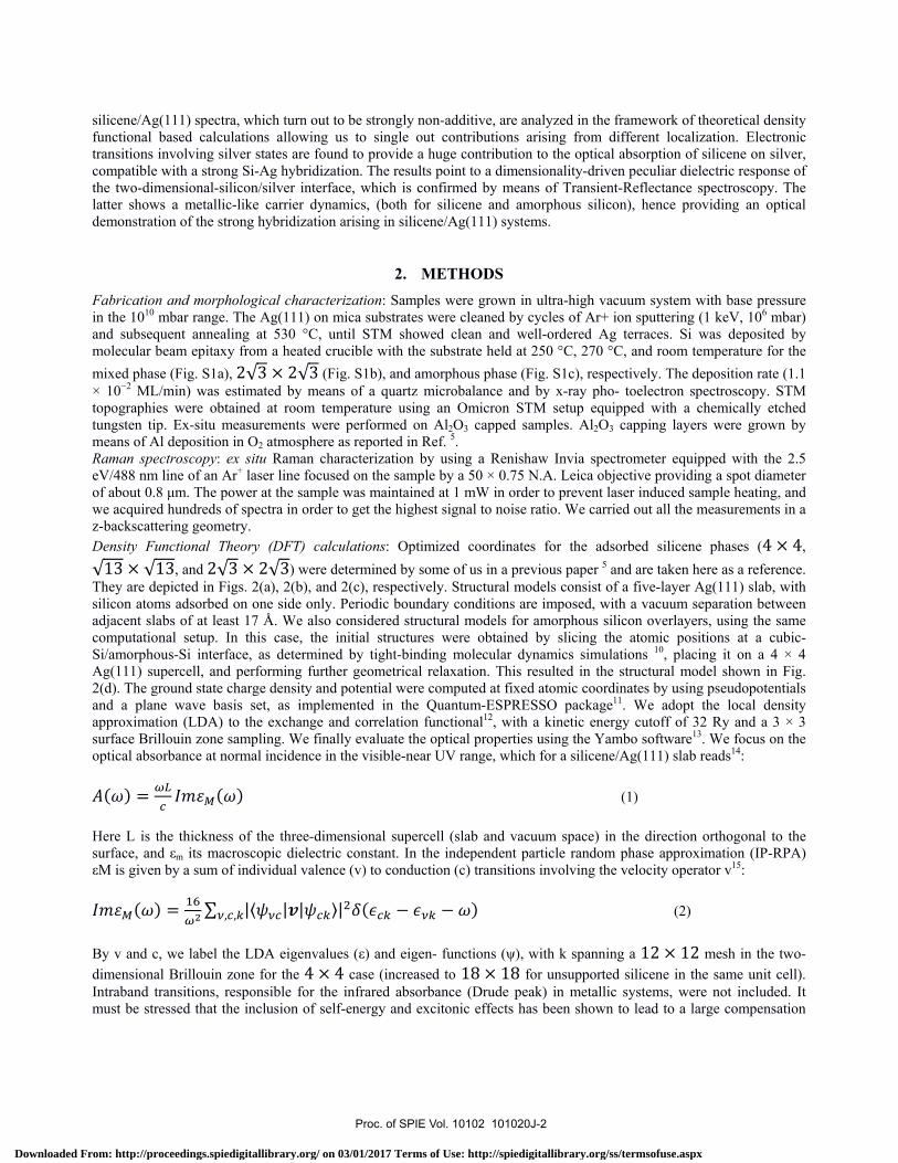
2. METHODS Fabrication and morphological characterization: Samples were grown in ultra-high vacuum system with base pressure in the 1010 mbar range. The Ag(111) on mica substrates were cleaned by cycles of Ar+ ion sputtering (1 keV, 106 mbar) and subsequent annealing at 530 °C, until STM showed clean and well-ordered Ag terraces. Si was deposited by molecular beam epitaxy from a heated crucible with the substrate held at 250 °C, 270 °C, and room temperature for the mixed phase (Fig. S1a), 2√3 × 2√3 (Fig. S1b), and amorphous phase (Fig. S1c), respectively. The deposition rate (1.1 × 10⁻² ML/min) was estimated by means of a quartz microbalance and by x-ray pho- toelectron spectroscopy. STM topographies were obtained at room temperature using an Omicron STM setup equipped with a chemically etched tungsten tip. Ex-situ measurements were performed on Al2O3 capped samples. Al2O3 capping layers were grown by means of Al deposition in O2 atmosphere as reported in Ref. 5. Raman spectroscopy: ex situ Raman characterization by using a Renishaw Invia spectrometer equipped with the 2.5 eV/488 nm line of an Ar+ laser line focused on the sample by a 50 × 0.75 N.A. Leica objective providing a spot diameter of about 0.8 μm. The power at the sample was maintained at 1 mW in order to prevent laser induced sample heating, and we acquired hundreds of spectra in order to get the highest signal to noise ratio. We carried out all the measurements in a z-backscattering geometry. Density Functional Theory (DFT) calculations: Optimized coordinates for the adsorbed silicene phases (4 × 4, √13 × √13, and 2√3 × 2√3) were determined by some of us in a previous paper 5 and are taken here as a reference. They are depicted in Figs. 2(a), 2(b), and 2(c), respectively. Structural models consist of a five-layer Ag(111) slab, with silicon atoms adsorbed on one side only. Periodic boundary conditions are imposed, with a vacuum separation between adjacent slabs of at least 17 Å. We also considered structural models for amorphous silicon overlayers, using the same computational setup. In this case, the initial structures were obtained by slicing the atomic positions at a cubic-Si/amorphous-Si interface, as determined by tight-binding molecular dynamics simulations 10, placing it on a 4 × 4 Ag(111) supercell, and performing further geometrical relaxation. This resulted in the structural model shown in Fig. 2(d). The ground state charge density and potential were computed at fixed atomic coordinates by using pseudopotentials and a plane wave basis set, as implemented in the Quantum-ESPRESSO package11. We adopt the local density approximation (LDA) to the exchange and correlation functional12, with a kinetic energy cutoff of 32 Ry and a 3 × 3 surface Brillouin zone sampling. We finally evaluate the optical properties using the Yambo software13. We focus on the optical absorbance at normal incidence in the visible-near UV range, which for a silicene/Ag(111) slab reads14: = (1) Here L is the thickness of the three-dimensional supercell (slab and vacuum space) in the direction orthogonal to the surface, and εm its macroscopic dielectric constant. In the independent particle random phase approximation (IP-RPA) εM is given by a sum of individual valence (v) to conduction (c) transitions involving the velocity operator v15: = ∑ | | | | − −, , (2) By v and c, we label the LDA eigenvalues (ε) and eigen- functions (ψ), with k spanning a 12 × 12 mesh in the two- dimensional Brillouin zone for the 4 × 4 case (increased to 18 × 18 for unsupported silicene in the same unit cell). Intraband transitions, responsible for the infrared absorbance (Drude peak) in metallic systems, were not included. It must be stressed that the inclusion of self-energy and excitonic effects has been shown to lead to a large compensation
Proc. of SPIE Vol. 10102 101020J-2
Downloaded From: http://proceedings.spiedigitallibrary.org/ on 03/01/2017 Terms of Use: http://spiedigitallibrary.org/ss/termsofuse.aspx
between the latter (electron-hole interaction) and the modification of the single-particle excitation energies16; also other silicon low-dimensional systems mostly exhibit a blue shift of the absorption peaks when going beyond IP-RPA17. Ultrafast spectroscopy measurements: We excited the sample with a broadband visible pulse, spectrally peaked around 500 nm, obtained from a visible optical parametric amplifier (OPA)18. We used as a probe the second harmonic of another OPA. Both OPAs were driven by an amplified Ti:sapphire laser system (500 μJ, 150 fs, 1 kHz). After chirped mirror compression, the duration of the pump pulse was less than 15 fs. We measured the probe reflection of the sample with an optical multichannel analyser working at the full repetition rate of the laser source. The acquisition of the pump-perturbed and pump-unperturbed probe spectra allowed us to extract the sample differential reflectivity ∆ ⁄ .
Figure 1. STM image showing the coexisting phases 4 × 4 and √13 × √13. (b) STM image of the 2√3 ×2√3. (c) STM image showing the amorphous Si grown at room temperature. Images are 30 × 30 nm2 wide and were acquired at sample bias Ubias = −1.5 V, −1 V, and −1.3 V and tunneling current I = 0.35 nA, 0.64 nA, and 0.4 nA, respectively.
3. RESULTS AND DISCUSSION
Fig. 3compares the typical Raman spectrum of multiphase epitaxial Silicene (where the 4 × 4, the 2√3 × 2√3 and √13 × √13 superstructures coexists), with those of an isolated 2√3 × 2√3 Silicene phase and of an amorphous silicon (a-Si) control sample. It is worth to notice how the Raman spectrum of the Silicene/Ag(111) system is completely different from the one of 1 ML equivalent a-Si, reported as a continuous curve in Fig. 3. This discrepancy can be easily understood if we take into account that silicene possess a crystalline order responsible for the narrow Raman peak (516 cm-1 and 522 cm-1 for the mixed phase and the isolated 2√3 × 2√3 phase respectively), whereas the a-Si bears only short-range order resulting in the typical broad Raman feature peaked at 480 cm-1. As reported elsewhere5, the spectrum in Fig. 3reflects the presence of differently oriented Silicene superstructures having slightly different atomic arrangements. The spectrum shows a sharp and intense E2g mode in the 515-522 cm-1 spectral range plus additional Raman-active and breathing-like A1g modes having different Raman intensities, accordingly with the buckling distribution of each silicene superstructure. Each Ag-supported silicene phase causes a perturbation of the D3d point group symmetry of the FS silicene that activates phase specific A1g modes and bears a phase dependent Raman behaviour as a function of the excitation wavelength5. Even tiny modifications on the bond length and bond angle distributions cause remarkable differences in the lattice response following the interaction with an external electric field.
Proc. of SPIE Vol. 10102 101020J-3
Downloaded From: http://proceedings.spiedigitallibrary.org/ on 03/01/2017 Terms of Use: http://spiedigitallibrary.org/ss/termsofuse.aspx
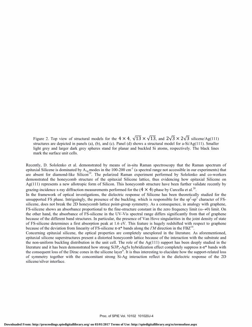
Figure 2structurelight gremark the
Recently, D. epitaxial Silicare absent fodemonstratedAg(111) reprgrazing-incidIn the framewunsupported silicene, doesFS-silicene shthe other hanbecause of thof FS-silicenbecause of thConcerning eepitaxial silicthe non-unifoliterature andthe consequenof symmetrysilicene/silver
2. Top view os are depictedy and larger
e surface unit c
Sololenko ecene is dominor diamond-l
d the honeycoresents a new dence x-ray difwork of opticFS phase. Ints not break thhows an abso
nd, the absorbhe different bae determines e deviation froepitaxial siliccene superstruorm buckling d it has been dnt loss of the D
y together wir interface.
of structural md in panels (a)dark grey sphcells.
et al. demonsated by A1g mike Silicon19.omb structureallotropic for
ffraction meascal investigattriguingly, thee 2D honeycorbance propor
bance of FS-siand structures.a first absorpom linearity oene, the optic
uctures presendistribution i
demonstrated hDirac cones inith the conco
models for th), (b), and (c)heres stand fo
trated by memodes in the 10
. The polarize of the epitarm of Siliconsurements perions, the diel
e presence of omb lattice portional to the ilicene in the . In particularption peak at of FS-silicene cal properties
nt a distorted hin the unit celhow strong Sin the silicene
omitant strong
he 4 × 4, √1. Panel (d) shor planar and
eans of in-situ00-200 cm-1 (azed Raman exaxial Silicene
n. This honeycrformed for thlectric responthe buckling,
oint-group symfine-structureUV-Vis spec
, the presence1.6 eV. This π-π* bands al
s are complethoneycomb lall. The role ofi3Pz-Ag5s hyblayer6. It is thg Si-Ag inter
13 × √13, hows a structud buckled Si a
u Raman spea spectral rangxperiment pee lattice, thuscomb structurhe (4 × 4) phnse of Silicene
which is respmmetry. As a e constant in thctral range dife of Van Hovefeature is huglong the ΓΜ dtely unexploreattice because f the Ag(111)bridization effus interesting raction reflec
and 2√3 ×
ural model foratoms, respect
ectroscopy thage not accessiberformed by s evidencing re have been fase by Curcele has been thponsible for tconsequence
he zero frequeffers significae singularities gely redshiftedirection in theed in the literof the interac
) support has fect completel
to elucidate ht in the diel
2√3 silicener a-Si/Ag(111)tively. The bl
at the Ramanble in our expSololenko anhow epitaxia
further validalla et al.20. heoretically stthe sp2-sp3 ch, in analogy wency limit (ω→antly from tha in the joint d
ed with respece FBZ14. rature. As afoction with thebeen deeply
ly suppress π-how the suppoectric respon
e/Ag(111) ). Smaller lack lines
n spectrum ofperiments) thand co-workersal Silicene onate recently by
tudied for theharacter of FSwith graphene→0) limit. Onat of graphenedensity of statect to graphene
forementionede substrate andstudied in theπ* bands with
ort-related lossnse of the 2D
f at s n y
e -
e, n e e e
d, d e h s
D
Proc. of SPIE Vol. 10102 101020J-4
Downloaded From: http://proceedings.spiedigitallibrary.org/ on 03/01/2017 Terms of Use: http://spiedigitallibrary.org/ss/termsofuse.aspx
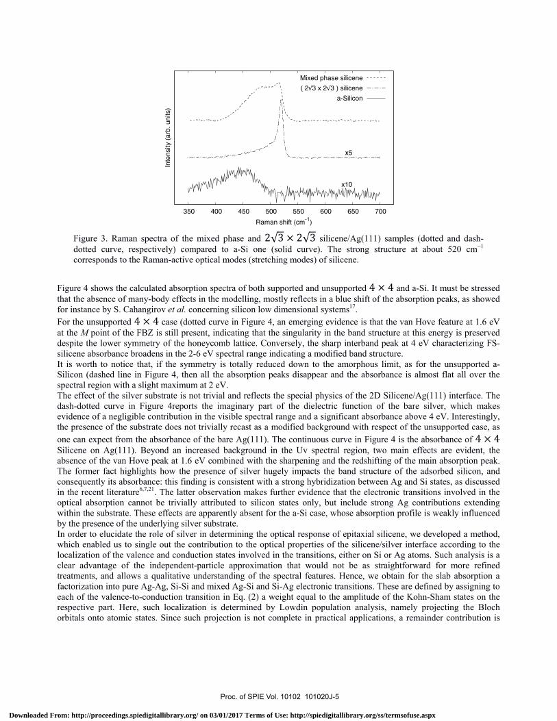
Figure 3. Raman spectra of the mixed phase and 2√3 × 2√3 silicene/Ag(111) samples (dotted and dash-dotted curve, respectively) compared to a-Si one (solid curve). The strong structure at about 520 cm−1 corresponds to the Raman-active optical modes (stretching modes) of silicene.
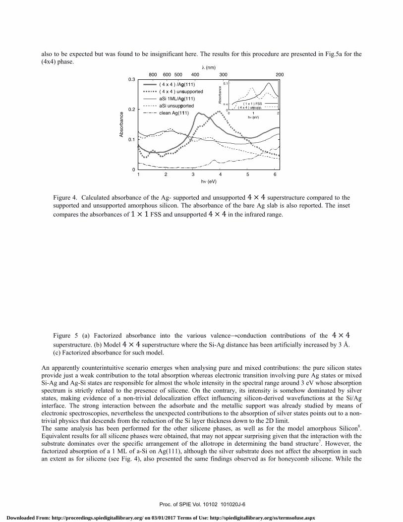
Figure 4 shows the calculated absorption spectra of both supported and unsupported 4 × 4 and a-Si. It must be stressed that the absence of many-body effects in the modelling, mostly reflects in a blue shift of the absorption peaks, as showed for instance by S. Cahangirov et al. concerning silicon low dimensional systems17. For the unsupported 4 × 4 case (dotted curve in Figure 4, an emerging evidence is that the van Hove feature at 1.6 eV at the M point of the FBZ is still present, indicating that the singularity in the band structure at this energy is preserved despite the lower symmetry of the honeycomb lattice. Conversely, the sharp interband peak at 4 eV characterizing FS-silicene absorbance broadens in the 2-6 eV spectral range indicating a modified band structure. It is worth to notice that, if the symmetry is totally reduced down to the amorphous limit, as for the unsupported a-Silicon (dashed line in Figure 4, then all the absorption peaks disappear and the absorbance is almost flat all over the spectral region with a slight maximum at 2 eV. The effect of the silver substrate is not trivial and reflects the special physics of the 2D Silicene/Ag(111) interface. The dash-dotted curve in Figure 4reports the imaginary part of the dielectric function of the bare silver, which makes evidence of a negligible contribution in the visible spectral range and a significant absorbance above 4 eV. Interestingly, the presence of the substrate does not trivially recast as a modified background with respect of the unsupported case, as one can expect from the absorbance of the bare Ag(111). The continuous curve in Figure 4 is the absorbance of 4 × 4 Silicene on Ag(111). Beyond an increased background in the Uv spectral region, two main effects are evident, the absence of the van Hove peak at 1.6 eV combined with the sharpening and the redshifting of the main absorption peak. The former fact highlights how the presence of silver hugely impacts the band structure of the adsorbed silicon, and consequently its absorbance: this finding is consistent with a strong hybridization between Ag and Si states, as discussed in the recent literature6,7,21. The latter observation makes further evidence that the electronic transitions involved in the optical absorption cannot be trivially attributed to silicon states only, but include strong Ag contributions extending within the substrate. These effects are apparently absent for the a-Si case, whose absorption profile is weakly influenced by the presence of the underlying silver substrate. In order to elucidate the role of silver in determining the optical response of epitaxial silicene, we developed a method, which enabled us to single out the contribution to the optical properties of the silicene/silver interface according to the localization of the valence and conduction states involved in the transitions, either on Si or Ag atoms. Such analysis is a clear advantage of the independent-particle approximation that would not be as straightforward for more refined treatments, and allows a qualitative understanding of the spectral features. Hence, we obtain for the slab absorption a factorization into pure Ag-Ag, Si-Si and mixed Ag-Si and Si-Ag electronic transitions. These are defined by assigning to each of the valence-to-conduction transition in Eq. (2) a weight equal to the amplitude of the Kohn-Sham states on the respective part. Here, such localization is determined by Lowdin population analysis, namely projecting the Bloch orbitals onto atomic states. Since such projection is not complete in practical applications, a remainder contribution is
Proc. of SPIE Vol. 10102 101020J-5
Downloaded From: http://proceedings.spiedigitallibrary.org/ on 03/01/2017 Terms of Use: http://spiedigitallibrary.org/ss/termsofuse.aspx
also to be exp(4x4) phase.
Figure 4supportedcompare
Figure 5superstru(c) Facto
An apparentlprovide just aSi-Ag and Agspectrum is sstates, makininterface. Thelectronic spetrivial physicThe same anEquivalent resubstrate domfactorized aban extent as
pected but wa
. Calculated d and unsupps the absorban
5 (a) Factoriucture. (b) Moorized absorba
ly counterintua weak contribg-Si states arestrictly relatedng evidence ohe strong inteectroscopies, ns that descend
nalysis has beesults for all siminates over sorption of a for silicene (s
as found to be
absorbance ofported amorphnces of 1 × 1
ized absorbanodel 4 × 4 suance for such m
uitive scenariobution to the
e responsible fd to the preseof a non-triviaeraction betwenevertheless tds from the redeen performedilicene phasesthe specific a1 ML of a-Sisee Fig. 4), al
e insignificant
f the Ag- supphous silicon. T1 FSS and uns
nce into theuperstructure wmodel.
o emerges whtotal absorpti
for almost the ence of silicenal delocalizateen the adsorthe unexpectedduction of thed for the oths were obtainearrangement oi on Ag(111), lso presented
t here. The res
ported and unThe absorbancsupported 4 ×
various valwhere the Si-A
hen analysing on whereas ewhole intensi
ne. On the coion effect infrbate and thed contribution
e Si layer thicker silicene ph
ed, that may nof the allotropalthough the the same find
sults for this p
nsupported 4ce of the bare× 4 in the infr
lence→conduAg distance ha
pure and mixlectronic tranity in the specontrary, its intfluencing silice metallic supns to the absorkness down tohases, as well
not appear surppe in determisilver substradings observe
procedure are
× 4 superstrue Ag slab is arared range.
ction contribas been artific
xed contributisition involvin
ctral range arotensity is somcon-derived wpport was alrrption of silveo the 2D limit.l as for the mprising given ining the banate does not afed as for hone
e presented in
ucture compaalso reported.
butions of thcially increase
ions: the pureng pure Ag st
ound 3 eV whomehow dominwavefunctionsready studied er states points. model amorphthat the intera
nd structure7. ffect the absoeycomb silice
Fig.5a for the
red to the The inset
he 4 × 4 ed by 3 Å.
e silicon statestates or mixedose absorption
nated by silvers at the Si/Ag
by means os out to a non
hous Silicon8
action with theHowever, the
orption in suchene. While the
e
s d n r g f -
8. e e h e
Proc. of SPIE Vol. 10102 101020J-6
Downloaded From: http://proceedings.spiedigitallibrary.org/ on 03/01/2017 Terms of Use: http://spiedigitallibrary.org/ss/termsofuse.aspx
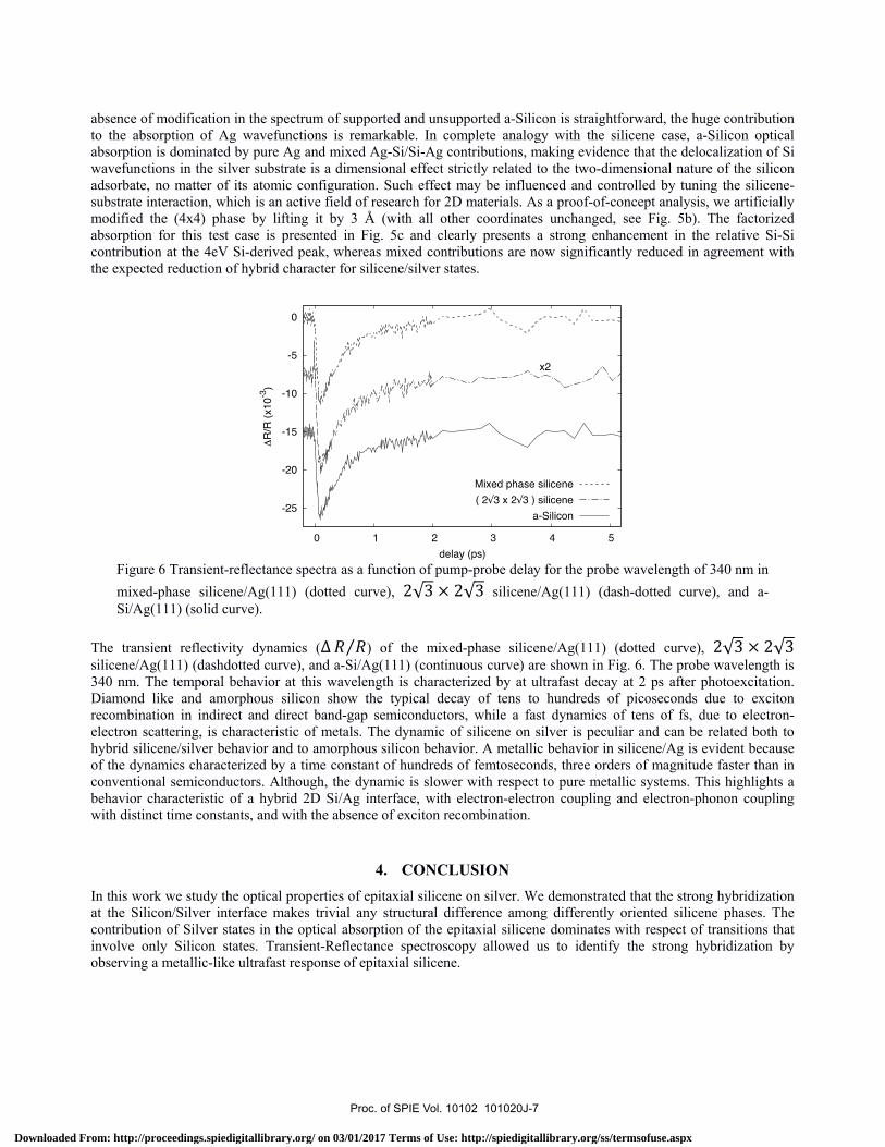
absence of modification in the spectrum of supported and unsupported a-Silicon is straightforward, the huge contribution to the absorption of Ag wavefunctions is remarkable. In complete analogy with the silicene case, a-Silicon optical absorption is dominated by pure Ag and mixed Ag-Si/Si-Ag contributions, making evidence that the delocalization of Si wavefunctions in the silver substrate is a dimensional effect strictly related to the two-dimensional nature of the silicon adsorbate, no matter of its atomic configuration. Such effect may be influenced and controlled by tuning the silicene-substrate interaction, which is an active field of research for 2D materials. As a proof-of-concept analysis, we artificially modified the (4x4) phase by lifting it by 3 Å (with all other coordinates unchanged, see Fig. 5b). The factorized absorption for this test case is presented in Fig. 5c and clearly presents a strong enhancement in the relative Si-Si contribution at the 4eV Si-derived peak, whereas mixed contributions are now significantly reduced in agreement with the expected reduction of hybrid character for silicene/silver states.
Figure 6 Transient-reflectance spectra as a function of pump-probe delay for the probe wavelength of 340 nm in mixed-phase silicene/Ag(111) (dotted curve), 2√3 × 2√3 silicene/Ag(111) (dash-dotted curve), and a-Si/Ag(111) (solid curve).
The transient reflectivity dynamics (∆ ⁄ ) of the mixed-phase silicene/Ag(111) (dotted curve), 2√3 × 2√3 silicene/Ag(111) (dashdotted curve), and a-Si/Ag(111) (continuous curve) are shown in Fig. 6. The probe wavelength is 340 nm. The temporal behavior at this wavelength is characterized by at ultrafast decay at 2 ps after photoexcitation. Diamond like and amorphous silicon show the typical decay of tens to hundreds of picoseconds due to exciton recombination in indirect and direct band-gap semiconductors, while a fast dynamics of tens of fs, due to electron-electron scattering, is characteristic of metals. The dynamic of silicene on silver is peculiar and can be related both to hybrid silicene/silver behavior and to amorphous silicon behavior. A metallic behavior in silicene/Ag is evident because of the dynamics characterized by a time constant of hundreds of femtoseconds, three orders of magnitude faster than in conventional semiconductors. Although, the dynamic is slower with respect to pure metallic systems. This highlights a behavior characteristic of a hybrid 2D Si/Ag interface, with electron-electron coupling and electron-phonon coupling with distinct time constants, and with the absence of exciton recombination.
4. CONCLUSION In this work we study the optical properties of epitaxial silicene on silver. We demonstrated that the strong hybridization at the Silicon/Silver interface makes trivial any structural difference among differently oriented silicene phases. The contribution of Silver states in the optical absorption of the epitaxial silicene dominates with respect of transitions that involve only Silicon states. Transient-Reflectance spectroscopy allowed us to identify the strong hybridization by observing a metallic-like ultrafast response of epitaxial silicene.
Proc. of SPIE Vol. 10102 101020J-7
Downloaded From: http://proceedings.spiedigitallibrary.org/ on 03/01/2017 Terms of Use: http://spiedigitallibrary.org/ss/termsofuse.aspx
REFERENCES
[1] Cahangirov, S., Topsakal, M., Aktürk, E., Şahin, H.., Ciraci, S., “Two- and One-Dimensional Honeycomb Structures of Silicon and Germanium,” Phys. Rev. Lett. 102(23) (2009). [2] Ezawa, M., “Valley-Polarized Metals and Quantum Anomalous Hall Effect in Silicene,” Phys. Rev. Lett. 109(5) (2012). [3] Vogt, P., De Padova, P., Quaresima, C., Avila, J., Frantzeskakis, E., Asensio, M. C., Resta, A., Ealet, B.., Le Lay, G., “Silicene: Compelling Experimental Evidence for Graphenelike Two-Dimensional Silicon,” Phys. Rev. Lett. 108(15) (2012). [4] Chiappe, D., Grazianetti, C., Tallarida, G., Fanciulli, M.., Molle, A., “Local Electronic Properties of Corrugated Silicene Phases,” Adv. Mater. 24(37), 5088–5093 (2012). [5] Cinquanta, E., Scalise, E., Chiappe, D., Grazianetti, C., van den Broek, B., Houssa, M., Fanciulli, M.., Molle, A., “Getting through the Nature of Silicene: An sp 2 –sp 3 Two-Dimensional Silicon Nanosheet,” J. Phys. Chem. C 117(32), 16719–16724 (2013). [6] Tsoutsou, D., Xenogiannopoulou, E., Golias, E., Tsipas, P.., Dimoulas, A., “Evidence for hybrid surface metallic band in (4 × 4) silicene on Ag(111),” Appl. Phys. Lett. 103(23), 231604 (2013). [7] Sheverdyaeva, P. M., Mahatha, S. K., Moras, P., Petaccia, L., Fratesi, G., Onida, G.., Carbone, C., “Electronic States of Silicene Allotropes on Ag(111),” ACS Nano 11(1), 975–982 (2017). [8] Cinquanta, E., Fratesi, G., dal Conte, S., Grazianetti, C., Scotognella, F., Stagira, S., Vozzi, C., Onida, G.., Molle, A., “Optical response and ultrafast carrier dynamics of the silicene-silver interface,” Phys. Rev. B 92(16), 165427 (2015). [9] Tao, L., Cinquanta, E., Chiappe, D., Grazianetti, C., Fanciulli, M., Dubey, M., Molle, A.., Akinwande, D., “Silicene field-effect transistors operating at room temperature,” Nat. Nanotechnol. 10(3), 227–231 (2015). [10] Santos, I., Cazzaniga, M., Onida, G.., Colombo, L., “Atomistic study of the structural and electronic properties of a-Si:H/c-Si interfaces,” J. Phys. Condens. Matter 26(9), 095001 (2014). [11] Giannozzi, P., Baroni, S., Bonini, N., Calandra, M., Car, R., Cavazzoni, C., Ceresoli, D., Chiarotti, G. L., Cococcioni, M., et al., “QUANTUM ESPRESSO: a modular and open-source software project for quantum simulations of materials,” J. Phys. Condens. Matter 21(39), 395502 (2009). [12] Perdew, J. P.., Zunger, A., “Self-interaction correction to density-functional approximations for many-electron systems,” Phys. Rev. B 23(10), 5048–5079 (1981). [13] Marini, A., Hogan, C., Grüning, M.., Varsano, D., “yambo: An ab initio tool for excited state calculations,” Comput. Phys. Commun. 180(8), 1392–1403 (2009). [14] Bechstedt, F., Matthes, L., Gori, P.., Pulci, O., “Infrared absorbance of silicene and germanene,” Appl. Phys. Lett. 100(26), 261906 (2012). [15] Onida, G., Reining, L.., Rubio, A., “Electronic excitations: density-functional versus many-body Green’s-function approaches,” Rev. Mod. Phys. 74(2), 601–659 (2002). [16] Wei, W.., Jacob, T., “Strong many-body effects in silicene-based structures,” Phys. Rev. B 88(4) (2013). [17] Cahangirov, S., Özçelik, V. O., Rubio, A.., Ciraci, S., “Silicite: The layered allotrope of silicon,” Phys. Rev. B 90(8) (2014). [18] Beutler, M., Ghotbi, M., Noack, F., Brida, D., Manzoni, C.., Cerullo, G., “Generation of high-energy sub-20 fs pulses tunable in the 250-310 nm region by frequency doubling of a high-power noncollinear optical parametric amplifier,” Opt. Lett. 34(6), 710 (2009). [19] Solonenko, D., Gordan, O. D., Lay, G. L., Şahin, H., Cahangirov, S., Zahn, D. R. T.., Vogt, P., “2D vibrational properties of epitaxial silicene on Ag(111),” 2D Mater. 4(1), 015008 (2016). [20] Curcella, A., Bernard, R., Borensztein, Y., Resta, A., Lazzeri, M.., Prévot, G., “Determining the atomic structure of the ( 4 × 4 ) silicene layer on Ag(111) by combined grazing-incidence x-ray diffraction measurements and first-principles calculations,” Phys. Rev. B 94(16) (2016). [21] Cahangirov, S., Audiffred, M., Tang, P., Iacomino, A., Duan, W., Merino, G.., Rubio, A., “Electronic structure of silicene on Ag(111): Strong hybridization effects,” Phys. Rev. B 88(3) (2013).
Proc. of SPIE Vol. 10102 101020J-8
Downloaded From: http://proceedings.spiedigitallibrary.org/ on 03/01/2017 Terms of Use: http://spiedigitallibrary.org/ss/termsofuse.aspx