Embed Size (px)
Citation preview
Ultrafast carrier response of Br1-irradiated In0.53Ga0.47As excitedat telecommunication wavelengths
L. Fekete,1 H. Nemec,1 Z. Mics,1 F. Kadlec,1 P. Kuzel,1,a) V. Novak,2 J. Lorincık,3,4
M. Martin,5 J. Mangeney,5 J. C. Delagnes,6 and P. Mounaix6
1Institute of Physics, ASCR, Na Slovance 2, 182 21 Prague 8, Czech Republic2Institute of Physics ASCR, Cukrovarnicka 10, 162 53 Prague 6, Czech Republic3Institute of Photonics and Electronics ASCR, Chaberska 57, 18251 Prague 8, Czech Republic4Department of Physics, Faculty of Science, J.E. Purkinje University, Ceske mladeze 8, 40096,Usti nad Labem, Czech Republic5Institut d’Electronique Fondamentale, Universite Paris XI, UMR CNRS 8622, 91405 Orsay Cedex, France6Laboratoire Ondes et Matiere d’Aquitaine, Universite Bordeaux I, UMR CNRS 5798,351 Cours de la Liberation, 33405 Talence Cedex, France
(Received 7 December 2011; accepted 27 March 2012; published online 10 May 2012)
We present results of infrared pump—terahertz probe experiments applied to a set of In0.53Ga0.47As
films irradiated with heavy ions (Brþ) at doses from 109 to 1012 cm�2. Photoexcitation at 1400 nm
(0.89 eV) allowed us to characterize the response close to telecommunications’ wavelengths whilst
avoiding the intervalley carrier scattering observed when a shorter wavelength excitation is used.
The excitation fluence was varied in our experiments in order to characterize the dynamics in detail:
the lifetimes and mobilities of both electrons and holes were retrieved, and the trap filling and
carrier diffusion were clearly observed. The In0.53Ga0.47As film irradiated by the dose of 1012 cm�2
exhibits simultaneously ultrashort electron lifetime (�300 fs) and very high electron mobility
(2800 cm2V�1s�1). These findings are particularly important for the design of terahertz emitters
controlled by lasers operating at standard telecommunication wavelengths. VC 2012 AmericanInstitute of Physics. [http://dx.doi.org/10.1063/1.4709441]
I. INTRODUCTION
In terahertz time-domain experiments and devices, the
opto-electronic approach to the generation of pulsed radia-
tion is typically based on optical rectification in nonlinear
crystals—such as non-centrosymmetric semiconductors like
GaAs, or ZnTe (Refs. 1 and 2)—or on photoswitching in
ultrafast semiconductors, e.g., in low-temperature-grown
GaAs.3,4 The choice of materials has been largely dictated
by the availability of Ti:sapphire femtosecond laser systems,
which operate at wavelengths near 800 nm. A promising
alternative to this rather robust approach is a combination of
less expensive femtosecond lasers operating at the telecom-
munication wavelength of 1.55 lm on the one hand, and
ultrafast semiconductors based on InGaAs (Ref. 5) or
organic crystals like 4-dimethylamino-N-methyl-4-stilbazo-
lium tosylate (DAST)6 on the other hand. DAST is mainly
used in broadband THz setups.7 However, the THz spectrum
emitted from a DAST crystal is compromised due to the
presence of a phonon mode at 1.1 THz.8
Materials suitable for efficient generation of THz
radiation by photoswitching should fulfill the following
requirements: (1) subpicosecond carrier lifetime, (2) high
photocarrier mobility, and (3) high dark electrical resistivity.
However, simultaneous optimization of these parameters is a
complex task, as it requires a feedback between material
growth technologies, the investigation of ultrafast carrier dy-
namics and the emitter preparation and testing.
Among the ultrafast semiconductors with a low band
gap, In0.53Ga0.47As (Eg¼ 0.74 eV) is a promising candidate
for THz photoswitches driven by radiation at wavelengths as
long as 1.67 lm. In this context, Be-doped low-temperature-
grown InGaAs,9 InGaAs film with embedded ErAs nano-
islands,10 Fe-doped InGaAs,11 Feþ ion,12 and heavy ion
irradiated InGaAs materials were investigated in the past,
and (sub)picosecond photocarrier response in these materials
was achieved.
In this paper, we use an infrared pump—THz probe
technique to study the ultrafast dynamics of electrons and
holes in In0.53Ga0.47As films grown on InP substrates and
irradiated by Brþ ions at high energies. This material was al-
ready tested for THz emission and detection in conjunction
with excitation at 800 nm and 1.55 lm wavelengths.13,14
However, in those experiments, only limited information
about the ultrafast response of the material was obtained. A
more detailed study of the material response was carried out
in our previous work;15 however, due to photoexcitation at
800 nm, intervalley carrier scattering strongly affected the
dynamics of electrons on the ultrafast time-scale.16 In the
current work, we avoid intervalley scattering by using low
excess energies of �140 meV (photoexcitation at 1.4 lm
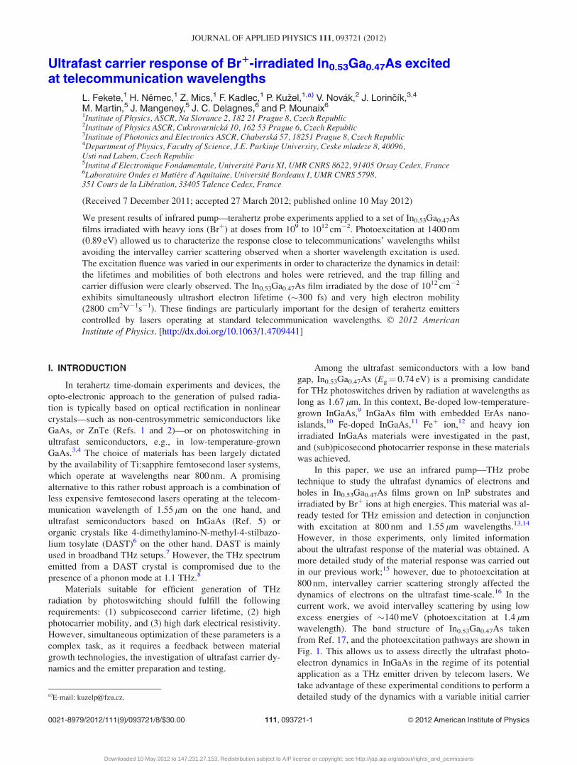
wavelength). The band structure of In0.53Ga0.47As taken
from Ref. 17, and the photoexcitation pathways are shown in
Fig. 1. This allows us to assess directly the ultrafast photo-
electron dynamics in InGaAs in the regime of its potential
application as a THz emitter driven by telecom lasers. We
take advantage of these experimental conditions to perform a
detailed study of the dynamics with a variable initial carriera)E-mail: [email protected].
0021-8979/2012/111(9)/093721/8/$30.00 VC 2012 American Institute of Physics111, 093721-1
JOURNAL OF APPLIED PHYSICS 111, 093721 (2012)
Downloaded 10 May 2012 to 147.231.27.153. Redistribution subject to AIP license or copyright; see http://jap.aip.org/about/rights_and_permissions
concentration in order to evaluate simultaneously the free-
electron and hole lifetimes and to determine the density of
traps.
II. SAMPLES
The undoped 3 -lm-thick In0.53Ga0.47As layers were
grown using gas source molecular-beam-epitaxy on a lattice-
matched semi-insulating InP:Fe substrate. After the growth,
the films were irradiated by 11 MeV Brþ ions at four differ-
ent doses of 109, 1010, 1011, and 1012 cm�2; these samples
are denoted A, B, C, and D, respectively, and they are
actually identical to the samples investigated in Ref. 15,
where the same notation was used.
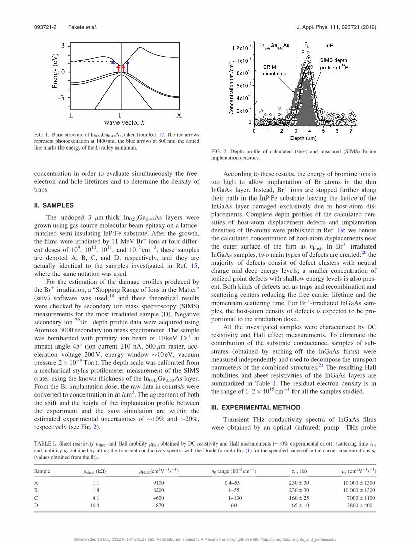
For the estimation of the damage profiles produced by
the Brþ irradiation, a “Stopping Range of Ions in the Matter”
(SRIM) software was used;18 and these theoretical results
were checked by secondary ion mass spectroscopy (SIMS)
measurements for the most irradiated sample (D). Negative
secondary ion 79Br� depth profile data were acquired using
Atomika 3000 secondary ion mass spectrometer. The sample
was bombarded with primary ion beam of 10 keV Csþ at
impact angle 45� (ion current 210 nA, 500 lm raster, acc-
eleration voltage 200 V, energy window �10 eV, vacuum
pressure 2� 10�9 Torr). The depth scale was calibrated from
a mechanical stylus profilometer measurement of the SIMS
crater using the known thickness of the In0.47Ga0.53As layer.
From the Br implantation dose, the raw data in counts/s were
converted to concentration in at./cm3. The agreement of both
the shift and the height of the implantation profile between
the experiment and the SRIM simulation are within the
estimated experimental uncertainties of �10% and �20%,
respectively (see Fig. 2).
According to these results, the energy of bromine ions is
too high to allow implantation of Br atoms in the thin
InGaAs layer. Instead, Brþ ions are stopped further along
their path in the InP:Fe substrate leaving the lattice of the
InGaAs layer damaged exclusively due to host-atom dis-
placements. Complete depth profiles of the calculated den-
sities of host-atom displacement defects and implantation
densities of Br-atoms were published in Ref. 19; we denote
the calculated concentration of host-atom displacements near
the outer surface of the film as nhost. In Brþ irradiated
InGaAs samples, two main types of defects are created:20 the
majority of defects consist of defect clusters with neutral
charge and deep energy levels; a smaller concentration of
ionized point defects with shallow energy levels is also pres-
ent. Both kinds of defects act as traps and recombination and
scattering centers reducing the free carrier lifetime and the
momentum scattering time. For Brþ-irradiated InGaAs sam-
ples, the host-atom density of defects is expected to be pro-
portional to the irradiation dose.
All the investigated samples were characterized by DC
resistivity and Hall effect measurements. To eliminate the
contribution of the substrate conductance, samples of sub-
strates (obtained by etching-off the InGaAs films) were
measured independently and used to decompose the transport
parameters of the combined structures.21 The resulting Hall
mobilities and sheet resistivities of the InGaAs layers are
summarized in Table I. The residual electron density is in
the range of 1–2� 1015 cm�1 for all the samples studied.
III. EXPERIMENTAL METHOD
Transient THz conductivity spectra of InGaAs films
were obtained by an optical (infrared) pump—THz probe
FIG. 1. Band structure of In0.53Ga0.47As, taken from Ref. 17. The red arrows
represent photoexcitation at 1400 nm, the blue arrows at 800 nm; the dotted
line marks the energy of the L-valley minimum.FIG. 2. Depth profile of calculated (SRIM) and measured (SIMS) Br-ion
implantation densities.
TABLE I. Sheet resistivity qsheet and Hall mobility lHall obtained by DC resistivity and Hall measurements (�10% experimental error); scattering time ss,e
and mobility le obtained by fitting the transient conductivity spectra with the Drude formula Eq. (1) for the specified range of initial carrier concentrations n0
(values obtained from the fit).
Sample qsheet (kX) lHall (cm2V�1s�1) n0 range (1015 cm�3) ss,e (fs) le (cm2V�1s�1)
A 1.1 9100 0.4–55 230 6 30 10 000 6 1300
B 1.8 8200 1–55 230 6 30 10 000 6 1300
C 4.1 4600 1–130 160 6 25 7000 6 1100
D 16.4 870 60 65 6 10 2800 6 400
093721-2 Fekete et al. J. Appl. Phys. 111, 093721 (2012)
Downloaded 10 May 2012 to 147.231.27.153. Redistribution subject to AIP license or copyright; see http://jap.aip.org/about/rights_and_permissions
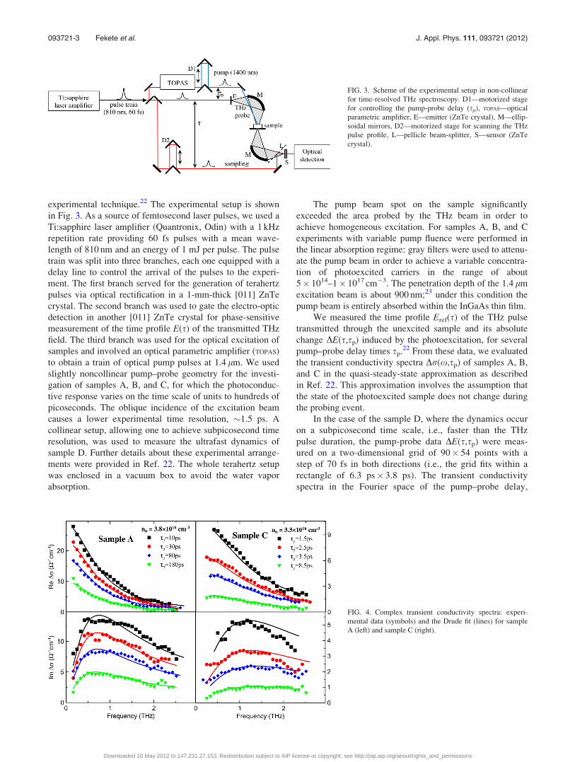
experimental technique.22 The experimental setup is shown
in Fig. 3. As a source of femtosecond laser pulses, we used a
Ti:sapphire laser amplifier (Quantronix, Odin) with a 1 kHz
repetition rate providing 60 fs pulses with a mean wave-
length of 810 nm and an energy of 1 mJ per pulse. The pulse
train was split into three branches, each one equipped with a
delay line to control the arrival of the pulses to the experi-
ment. The first branch served for the generation of terahertz
pulses via optical rectification in a 1-mm-thick [011] ZnTe
crystal. The second branch was used to gate the electro-optic
detection in another [011] ZnTe crystal for phase-sensitive
measurement of the time profile E(s) of the transmitted THz
field. The third branch was used for the optical excitation of
samples and involved an optical parametric amplifier (TOPAS)
to obtain a train of optical pump pulses at 1.4 lm. We used
slightly noncollinear pump–probe geometry for the investi-
gation of samples A, B, and C, for which the photoconduc-
tive response varies on the time scale of units to hundreds of
picoseconds. The oblique incidence of the excitation beam
causes a lower experimental time resolution, �1.5 ps. A
collinear setup, allowing one to achieve subpicosecond time
resolution, was used to measure the ultrafast dynamics of
sample D. Further details about these experimental arrange-
ments were provided in Ref. 22. The whole terahertz setup
was enclosed in a vacuum box to avoid the water vapor
absorption.
The pump beam spot on the sample significantly
exceeded the area probed by the THz beam in order to
achieve homogeneous excitation. For samples A, B, and C
experiments with variable pump fluence were performed in
the linear absorption regime: gray filters were used to attenu-
ate the pump beam in order to achieve a variable concentra-
tion of photoexcited carriers in the range of about
5� 1014–1� 1017 cm�3. The penetration depth of the 1.4 lm
excitation beam is about 900 nm;23 under this condition the
pump beam is entirely absorbed within the InGaAs thin film.
We measured the time profile Eref(s) of the THz pulse
transmitted through the unexcited sample and its absolute
change DE(s,sp) induced by the photoexcitation, for several
pump–probe delay times sp.22 From these data, we evaluated
the transient conductivity spectra Dr(x,sp) of samples A, B,
and C in the quasi-steady-state approximation as described
in Ref. 22. This approximation involves the assumption that
the state of the photoexcited sample does not change during
the probing event.
In the case of the sample D, where the dynamics occur
on a subpicosecond time scale, i.e., faster than the THz
pulse duration, the pump-probe data DE(s,sp) were meas-
ured on a two-dimensional grid of 90� 54 points with a
step of 70 fs in both directions (i.e., the grid fits within a
rectangle of 6.3 ps� 3.8 ps). The transient conductivity
spectra in the Fourier space of the pump–probe delay,
FIG. 3. Scheme of the experimental setup in non-collinear
for time-resolved THz spectroscopy. D1—motorized stage
for controlling the pump-probe delay (sp), TOPAS—optical
parametric amplifier, E—emitter (ZnTe crystal), M—ellip-
soidal mirrors, D2—motorized stage for scanning the THz
pulse profile, L—pellicle beam-splitter, S—sensor (ZnTe
crystal).
FIG. 4. Complex transient conductivity spectra: experi-
mental data (symbols) and the Drude fit (lines) for sample
A (left) and sample C (right).
093721-3 Fekete et al. J. Appl. Phys. 111, 093721 (2012)
Downloaded 10 May 2012 to 147.231.27.153. Redistribution subject to AIP license or copyright; see http://jap.aip.org/about/rights_and_permissions

Dr(x,xp), were then calculated, see Refs. 22 and 24 for fur-
ther details.
In addition, THz kinetics representing the evolution
of spectrally averaged THz photoconductivity versus pump–
probe delay was obtained for samples A, B, and C. Here, the
maximum of the transient terahertz waveform DE(smax,sp)
was directly recorded as a function of sp. Subsequently, we
measured a series of waveforms DE(s,sp) for a few pump-
probe delays sp under the same experimental conditions.
Their interpolation with a weight DE(smax,sp) was then used
to evaluate the spectra DE(x,sp) for any sp and hence we
obtained the time-evolution of spectra of the transient con-
ductivity Dr(x,sp). The results of such measurements will
be discussed in Sec. V.
IV. SPECTRAL RESPONSE
The transient conductivity spectra of samples A, B, and
C were fitted using the Drude formula for conductivity due
to one type of free carriers (see Fig. 4). This approximation
can be applied for short or medium pump–probe delays as
electrons are significantly more mobile than holes. The
Drude formula for the electrons then reads
Drðx; spÞ ¼ nðspÞe0
le
1� ixss;e: (1)
Here, e0 is the elementary charge, n(sp) is the free electron
density exhibiting decay due to trapping and recombination,
and ss,e is the electron momentum relaxation time. The term
le¼ e0ss,e/meff is the dc photoelectron mobility (the effective
mass of electrons in In0.53Ga0.47As at the bottom of C-valley
is meff¼ 0.041 me (Ref. 25)). Fitting the transient conductiv-
ity spectra with the Drude term yields values of ss,e and le.
The scattering time ss was found to be independent of the
carrier density for the range of pump fluences used. The ini-
tial carrier concentration n0 : n(0) obtained from the fit was
found to be about twice as small as that estimated from the
measured incident pump photon flux which is a reasonable
agreement. The values are summarized in Table I.
The sample D irradiated with the highest dose exhibits
subpicosecond carrier lifetime. A two-dimensional spectral
map of the transient photoconductivity Dr(x,xp) is displayed
in Figs. 5(a), 5(c), and 5(e). The monotonous decrease of the
amplitude of the photoinduced conductivity Dr(x, xp) along
the x axis, observed in Fig. 5(e), indicates the Drude response
of the carriers.26 The marked decrease of conductivity with
increasing jxpj is a clear signature of ultrashort carrier life-
time. To fit the data, we assumed exponential decay of the
free carrier concentration with the lifetime sc26,27
Drðx;xpÞ ¼n0e2
0ss;e
meff
� 1
1þ ss;e
sc� ixss;e
� 11sc� ixp
: (2)
This expression was used to simultaneously fit the real and
imaginary parts of the experimental data [Figs. 5(a)–5(d)].
The featureless residuals of the fit displayed in Fig. 5(f)
indicate a very good agreement between the measured data
and the model. The parameters ss,e and n0 are provided in
Table I; the carrier lifetime was found to be sc¼ 300 fs. Note
that this short carrier lifetime is accompanied by a relatively
high photocarrier mobility of 2800 cm2V�1s�1. For compari-
son, in In0.53Ga0.47As films with embedded ErAs nanoislands
a lifetime of about 3 ps was found by time-resolved
THz spectroscopy and the reported Hall mobility was
�400 cm2V�1s�1. In In0.53Ga0.47As:ErAs superlattices, the
picosecond carrier lifetime can be also substantially dec-
reased by additional Be-doping.28 A lifetime as low as 300 fs
was found for high Be-doping levels,28 while the Hall mobil-
ity of electrons in this case decreased to a value of the order
of hundreds cm2V�1s�1.29
Finally, we comment on the difference between the Hall
mobility and the mobility of photoexcited electrons which
are provided in the 3 rd and 6th columns of Table I. The Hall
FIG. 5. Transient conductivity spectra of the sample D in the two-
dimensional frequency domain (in X�1 THz�1 m�1). (a) real part measured
and (b) fitted, respectively; (c) and (d) imaginary part measured and fitted,
respectively; (e) and (f) amplitude of the complex conductivity measured
and fitted, respectively; and (g) residuals of a complex fit. The complex fit-
ting was done by using Eq. (2) which assumes an exponential decay of the
free carrier concentration with the lifetime sc.
093721-4 Fekete et al. J. Appl. Phys. 111, 093721 (2012)
Downloaded 10 May 2012 to 147.231.27.153. Redistribution subject to AIP license or copyright; see http://jap.aip.org/about/rights_and_permissions

mobility is a low electric field mobility obtained with low
densities of carriers (1015 cm�3), whereas the mobility result-
ing from our THz measurements is a single carrier response
function of photoexcited electrons measured at higher con-
centrations. In samples with a large density of defects some
equilibrium (dark) carriers can spend a large amount of time
in lower-mobility states during the measurements while at
the early stages after their creation, the large majority of pho-
toexcited electrons are highly mobile. Therefore, the defect
scattering due to irradiation process affects more the Hall
mobility as deduced from Table I.
V. DYNAMICS OF ELECTRONS AND HOLES
Here, we report the experimental data representing the
evolution of THz photoconductivity versus pump–probe
delay. Experimentally, we found out that the dynamics of the
carrier population depend on the initial carrier concentration
and on the concentration of traps created by the Brþ irradia-
tion. For samples A, B, and C, we observed a slowing down
of the measured kinetics by a factor of about 1.2–2 within
the range of the pump fluence used in our experiments. We
attribute this effect to trap filling and to carrier diffusion in
the direction perpendicular to the surface.
In the first approximation and in order to compare the
dynamics of the samples A, B, and C, the decay times sc
were estimated from the fits by a single-exponential decay of
the carrier concentration for each individual pump fluence /:
n(sp,/)¼ n0(/) exp(� sp/sc). For the sample A, sc increases
with increasing excitation intensities from 116 to 185 ps; for
sample B, we find an increase of sc from 23 to 28 ps; and for
sample C, sc increases from 1.5 to 3 ps.
The electron diffusion length is defined as
lD �ffiffiffiffiffiffiffiffiffiffiffiffiffiffiffiffikBTss
meffsc
s; (3)
where T is the carrier temperature and kB is the Boltzmann
constant. In this way, we obtain the following estimations
for sample A: lD¼ 1.7–2.2 lm, B: lD¼ 0.75–0.85 lm, and
C: lD¼ 0.16–0.22 lm. This implies that for samples A and
B, the diffusion length is longer than or comparable to the
absorption length of the excitation beam (0.9 lm). A signifi-
cant part of the photogenerated carriers may thus diffuse
away from regions close to the sample input surface (where,
for high pump fluences, the traps may become filled soon af-
ter photoexcitation) into deeper regions of the layer where
the traps are nearly empty. In the case of sample C, where
the electron diffusion length is smaller than the penetration
depth of the excitation light, the kinetics is expected to be
mainly determined by the trap filling and the depletion via
the recombination of carriers.
To model the dynamics of electrons and holes in more
detail, we adopted the model successfully used for the
description of ultrafast carrier dynamics in Brþ-irradiated
InP.19 The model consists of a set of coupled kinetic equa-
tions which involve both the trap filling effect and the diffu-
sion perpendicular to the sample surface (steepest gradient
along the z-direction). The densities of free electrons (ne),
trapped electrons (nt), and free holes (nh) become inhomoge-
neous and depend on z. The model contains six important
unknown parameters: the density of traps (Nt), the position
of trap levels below the conduction band minimum (Et), the
lifetime of electrons (se) and that of holes (sh), and the scat-
tering time of electrons and holes (ss,e and ss,h); the diffusion
coefficient of electrons (holes) is assumed to be given by the
Einstein relation De,h¼ kBTle,h/e0.
@ne
@t¼ De
@2ne
@z2� ne
se1� nt
Nt
� �þ gent
@nt
@t¼ ne
se1� nt
Nt
� �� nh
sh� nt
Nt� ntðge þ ghÞ
@nh
@t¼ Dh
@2nh
@z2� nh
sh� nt
Ntþ ghnt
(4)
The release rates ge and gh of the carriers are described by
the Shockley-Read model,30
ge¼1
se�Ne
Ntctexp � Et
kBT
� �;
gh¼1
sh�Nh
Ntc�1
t exp �Eg�Et
kBT
� �;
(5)
and depend on the effective density of states of electrons and
holes (Ne and Nh), and on the position of trap level below the
conduction band minimum Et. The degeneracy factor ct is
assumed to be unity.
The total transient conductivity of photoexcited InGaAs
layer defined by our model includes contributions from both
electrons and holes and reads
Drðx; sp;/Þ ¼ e0
ðL
0
dz½leðxÞneðz; sp;/Þ
þ lhðxÞnhðz; sp;/Þ�; (6)
where L¼ 3 lm is the thickness of InGaAs layer. Note that the
conductivity and free-carrier concentrations now depend on
the excitation fluence /. The conductivity defined by Eq. (6)
was convoluted with an instrumental function related to the
noncollinear arrangement of the pump–probe experiment
(Gaussian function in sp with a full-width-at-half-maximum of
1.5 ps). The result was fitted to the measured pump–probe
scans of the transient conductivity; examples of the data and
fits are shown in Fig. 6. The parameters for electrons (ss,e and
le) and the initial concentration of electron-hole pairs, n0,
were estimated from the Drude spectral response described in
the previous part, and they were kept fixed during the fit. The
results of our fits are displayed in Table II.
The kinetics observed for each sample (A, B, and C) can
be explained by taking into account an interplay of two proc-
esses: the trap filling and the carrier diffusion; these occur with
different weights for each of the samples. The Shockley-Read
terms Eq. (5) have not been found to have a significant impact
on the observed carrier dynamics and can practically be
neglected. We can thus infer that the trap level is sufficiently
deep below the conduction band edge to prevent significant
093721-5 Fekete et al. J. Appl. Phys. 111, 093721 (2012)
Downloaded 10 May 2012 to 147.231.27.153. Redistribution subject to AIP license or copyright; see http://jap.aip.org/about/rights_and_permissions
thermal activation of the trapped carriers, and we can roughly
estimate Nt� 0.3 eV.
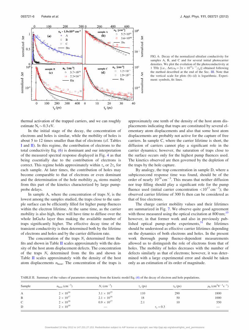
In the initial stage of the decay, the concentration of
electrons and holes is similar, while the mobility of holes is
about 5 to 12 times smaller than that of electrons (cf. Tables
I and II). In this regime, the contribution of electrons to the
total conductivity Eq. (6) is dominant and our interpretation
of the measured spectral response displayed in Fig. 4 as that
being essentially due to the contribution of electrons is
correct. This regime holds approximately within se or 2se for
each sample. At later times, the contribution of holes may
become comparable to that of electrons or even dominant
and the determination of the hole mobility lh stems mainly
from this part of the kinetics characterized by large pump-
probe delays.
In sample A, where the concentration of traps Nt is the
lowest among the samples studied, the traps close to the sam-
ple surface can be efficiently filled for higher pump fluences
within the electron lifetime. At the same time, as the carrier
mobility is also high, these will have time to diffuse over the
whole InGaAs layer thus making the available number of
traps significantly higher. The effective decay time of the
transient conductivity is then determined both by the lifetime
of electrons and holes and by the carrier diffusion rate.
The concentration of the traps Nt determined from the
fits and shown in Table II scales approximately with the den-
sity of the host atom displacement defects. The concentration
of the traps Nt determined from the fits and shown in
Table II scales approximately with the density of the host
atom displacements nhost. The concentration of the traps is
approximately one tenth of the density of the host atom dis-
placements indicating that traps are constituted by several el-
ementary atom displacements and also that some host atom
displacements are probably not active for the capture of free
carriers. In sample C, where the carrier lifetime is short, the
diffusion of carriers cannot play a significant role in the
carrier dynamics; however, the saturation of traps close to
the surface occurs only for the highest pump fluences used.
The kinetics observed are then governed by the depletion of
the traps by the hole capture.
By analogy, the trap concentration in sample D, where a
subpicosecond response time was found, should be of the
order of nearly 1018 cm�3. This means that neither diffusion
nor trap filling should play a significant role for the pump
fluence used (initial carrier concentration <1017 cm�3); the
observed carrier lifetime of 300 fs then can be considered as
that of free electrons.
The charge carrier mobility values and their lifetimes
are summarized in Fig. 7. We observe quite good agreement
with those measured using the optical excitation at 800 nm;15
however, in that former work and also in previously pub-
lished optical pump–probe experiments,31 the lifetimes
should be understood as effective carrier lifetimes depending
on the dynamics of both electrons and holes. In the present
work thorough pump fluence-dependent measurements
allowed us to distinguish the role of electrons from that of
holes. The mobility of holes decreases with the number of
defects similarly as that of electrons; however, it was deter-
mined with a large experimental error and should be taken
only as an estimation of its order of magnitude.
FIG. 6. Decay of the normalized ultrafast conductivity for
samples A, B, and C and for several initial photocarrier
densities. We plot the evolution of the photoconductivity at
1 THz [i.e., Dr(x0¼ 2p� 1012s�1,sp)] obtained following
the method described at the end of the Sec. III. Note that
the vertical scale for plots (b)–(d) is logarithmic. Experi-
ment: symbols, fit: lines.
TABLE II. Summary of the values of parameters stemming from the kinetic model Eq. (4) of the decay of electron and hole populations.
Sample nhost (cm�3) Nt (cm�3) se (ps) sh (ps) lh (cm2V�1s�1)
A 2 � 1016 3.1 � 1015 110 290 1800
B 2 � 1017 2.1 � 1016 18 50 1000
C 2 � 1018 0.9 � 1017 2.1 10 550
D 2 � 1019 — sc¼ 0.3 —
093721-6 Fekete et al. J. Appl. Phys. 111, 093721 (2012)
Downloaded 10 May 2012 to 147.231.27.153. Redistribution subject to AIP license or copyright; see http://jap.aip.org/about/rights_and_permissions
VI. CONCLUSION
We have investigated the dynamics of photogenerated
carriers in In0.53Ga0.47As films irradiated by heavy high-
energy Brþ ions using infrared pump–THz probe spectros-
copy. To shed more light on the dynamics of both electrons
and holes, the samples were excited at 1400 nm wavelength,
and the pump fluences were varied within 2.5 orders of mag-
nitude to achieve free carrier density from 5�1014 to
1�1017 cm�3. The electron and hole lifetimes and mobilities
were determined within a kinetic model, which accounts for
the carrier diffusion within the InGaAs film and for the trap
filling at high photocarrier densities. Both the carrier lifetimes
and the density of traps are approximately proportional to the
concentration of the host atom displacement defects. It was
found that the In0.53Ga0.47As film irradiated by the dose of
1012 cm–2 exhibits simultaneously ultrashort electron lifetime
(�300 fs) and very high electron mobility (2800 cm2V–1s–1)
which makes this material a promising candidate for the fabri-
cation of THz emitters and detectors controlled by lasers oper-
ating at telecommunication wavelengths.
ACKNOWLEDGMENTS
The financial support by the Czech Science Foundation
(Project No 202/09/P099), by ASCR and its Grant Agency
(Project Nos. AVOZ10100520 and A100100902), and by the
Ministry of Education of the Czech Republic (Project No.
LC-512) are acknowledged.
1A. Nahata, A. S. Weling, and T. F. Heinz, “A wideband coherent terahertz
spectroscopy system using optical rectification and electro-optic
sampling,” Appl. Phys. Lett. 69, 2321 (1996).2A. Rice, Y. Jin, X. F. Ma, X. C. Zhang, D. Bliss, J. Larkin, and
M. Alexander, “Terahertz optical rectification from h110i zinc-blende
crystals,” Appl. Phys. Lett. 64, 1324 (1994).3S. Gupta, M. Y. Frankel, J. A. Valdmanis, J. F. Whitaker, and G. A.
Mourou, “Subpicosecond carrier lifetime in GaAs grown by molecular
beam epitaxy at low temperatures,” Appl. Phys. Lett. 59, 3276 (1991).4H. Nemec, A. Pashkin, P. Kuzel, M. Khazan, S. Schnull, and I. Wilke,
“Carrier dynamics in low-temperature grown GaAs studied by terahertz
emission spectroscopy,” J. Appl. Phys. 90, 1303 (2001).5N. Chimot, J. Mangeney, L. Joulaud, P. Crozat, H. Bernas, K. Blary, and
J. F. Lampin, “Terahertz radiation from heavy-ion-irradiated
In0.53Ga0.47As photoconductive antenna excited at 1.55 lm,” Appl.
Phys. Lett. 87, 193510 (2005).
6M. Martin, J. Mangeney, P. Crozat, and P. Mounaix, “Optical phase detec-
tion in a 4-N,N-dimethylamino-4’-N’-methyl-stilbazolium tosylate crystal
for terahertz time domain spectroscopy system at 1.55 lm wavelength,”
Appl. Phys. Lett. 97, 111112 (2010).7A. Schneider, M. Stillhart, and P. Gunter, “High efficiency generation and
detection of terahertz pulses using laser pulses at telecommunication
wavelengths,” Opt. Express 14, 5376 (2006).8A. Schneider, M. Neis, M. Stillhart, B. Ruiz, R. U. A. Khan, and P. Gunter,
“Generation of terahertz pulses through optical rectification in organic DAST
crystals: Theory and experiment,” J. Opt. Soc. Am. B 23, 1822 (2006).9A. Takazato, M. Kamakura, T. Matsui, J. Kitagawa, and Y. Kadoya,
“Detection of terahertz waves using low-temperature-grown InGaAs with
1.56 lm pulse excitation,” Appl. Phys. Lett. 90, 101119 (2007).10A. K. Azad, R. P. Prasankumar, D. Talbayev, A. J. Taylor, R. D. Averitt,
J. M. O. Zide, H. Lu, A. C. Gossard, and J. F. O’Hara, “Carrier dynamics
in InGaAs with embedded ErAs nanoislands,” Appl. Phys. Lett. 93,
121108 (2008).11C. D. Wood, O. Hatem, J. E. Cunningham, E. H. Linfield, A. G. Davies,
P. J. Cannard, M. J. Robertson, and D. G. Moodie, “Terahertz emission
from metal-organic chemical vapor deposition grown Fe:InGaAs using
830 nm to 1.55 lm excitation,” Appl. Phys. Lett. 96, 194104 (2010).12M. Suzuki and M. Tonouchi, “Fe-implanted InGaAs photoconductive tera-
hertz detectors triggered by 1.56 lm femtosecond optical pulses,” Appl.
Phys. Lett. 86, 163504 (2005).13N. Chimot, J. Mangeney, P. Mounaix, M. Tondusson, K. Blary, and J. F.
Lampin, “Terahertz radiation generated and detected by Brþ-irradiated
In0.53Ga0.47As photoconductive antenna excited at 800 nm wavelength,”
Appl. Phys. Lett. 89, 083519 (2006).14J. Mangeney, N. Chimot, L. Meignien, N. Zerounian, P. Crozat, K. Blary,
J. F. Lampin, and P. Mounaix, “Emission characteristics of ion-irradiated
In0.53Ga0.47As based photoconductive antennas excited at 1.55 lm,” Opt.
Express 156, 8943 (2007).15J. C. Delagnes, P. Mounaix, H. Nemec, L. Fekete, F. Kadlec, P. Kuzel,
M. Martin, and J. Mangeney, “High photocarrier mobility in ultrafast ion-
irradiated In0.53Ga0.47As for terahertz applications,” J. Phys. D: Appl.
Phys. 42, 195103 (2009).16S. E. Ralph, Y. Chen, J. Woodall, and D. McInturff, “Subpicosecond pho-
toconductivity of In0.53Ga0.47As: Intervalley scattering rates observed via
THz spectroscopy,” Phys. Rev. B 54, 5568 (1996).17R. Dittrich and W. Schroeder, “Empirical pseudopotential band structure
of In0.53Ga0.47As and In0.52Al0.48As,” Solid-State Electron. 43, 403 (1999).18J. P. Biersack and L. G. Haggmark, “A Monte Carlo computer program for
the transport of energetic ions in amorphous targets,” Nucl. Instrum. Meth-
ods 174, 257 (1980).19H. Nemec, L. Fekete, F. Kadlec, P. Kuzel, M. Martin, J. Mangeney, J. C.
Delagnes, and P. Mounaix, “Ultrafast carrier dynamics in Brþ-bombarded
InP studied by time-resolved terahertz spectroscopy,” Phys. Rev. B. 78,
235206 (2008).20L. Joulaud, J. Mangeney, L. M. Lourtioz, P. Crozat, and G. Patriarche,
“Thermal stability of ion-irradiated InGaAs with (sub-) picosecond carrier
lifetime,” Appl. Phys. Lett. 82, 856 (2003).21D. K. Schroder, Semiconductor Material and Device Characterization, 3rd
ed. (Wiley, 2006), p. 97.22L. Fekete, P. Kuzel, H. Nemec, F. Kadlec, A. Dejneka, J. Stuchlık, and
A. Fejfar, “Ultrafast carrier dynamics in microcrystalline silicon probed by
time-resolved terahertz spectroscopy,” Phys. Rev. B 79, 115306 (2009).23D. A. Humphreys, R. J. King, D. Jenkins, and A. J. Moseley,
“Measurement of absorption coefficients of Ga0.47In0.53As over the wave-
length range 1.0–1.7 lm,” Electron. Lett. 21, 1187 (1985); E. Zielinski,
H. Schweizer, K. Streubel, H. Eisele, and G. Weimann, “Excitonic transi-
tions and exciton damping processes in InGaAs/InP,” J. Appl. Phys. 59,
2196 (1985).24P. Kuzel, F. Kadlec, and H. Nemec, “Propagation of terahertz pulses in
photoexcited media: Analytical theory for layered systems,” J. Chem.
Phys. 127, 024506 (2007).25Handbook Series on Semiconductor Parameters, edited by M. Levinshtein,
S. Rumyantsev, and M. Shur (World Scientific, Singapore, 1999), Vol. 2,
p. 62.26H. Nemec, F. Kadlec, S. Surendran, P. Kuzel, and P. Jungwirth, “Ultrafast
far-infrared dynamics probed by terahertz pulses: A frequency-domain
approach. I. Model systems,” J. Chem. Phys. 122, 104503 (2005).27H. Nemec, F. Kadlec, C. Kadlec, P. Kuzel, and P. Jungwirth, “Ultrafast
far-infrared dynamics probed by terahertz pulses: A frequency-domain
approach. II. Applications,” J. Chem. Phys. 122, 104504 (2005).
FIG. 7. Comparison of (a) carrier lifetimes [sc is effective carrier lifetime
obtained in experiments with photoexcitation at 800 nm,15 se is the lifetime
of electrons, and sh is the lifetime of holes] and (b) mobilities [lc refers to
Ref. 15, le is the mobility of electrons, and lh is the mobility of holes] as a
function of host-atom displacement concentration. Closed symbols: excita-
tion at 800 nm;15 open symbols: excitation at 1400 nm.
093721-7 Fekete et al. J. Appl. Phys. 111, 093721 (2012)
Downloaded 10 May 2012 to 147.231.27.153. Redistribution subject to AIP license or copyright; see http://jap.aip.org/about/rights_and_permissions

28D. C. Driscoll, M. P. Hanson, A. C. Gossard, and E. R. Brown, “Ultrafast
photoresponse at 1.55 lm in InGaAs with embedded semimetallic ErAs
nanoparticles,” Appl. Phys. Lett. 86, 051908 (2005).29D. C. Driscoll, M. P. Hanson, and A. C. Gossard, “Carrier compensation in semi-
conductors with buried metallic nanoparticles,” J. Appl. Phys. 97, 016102 (2005).
30W. Shockley and W. T. Read, “Statistics of the recombinations of holes
and electrons,” Phys. Rev. 87, 835 (1952).31J. Mangeney and P. Crozat, “Ion-irradiated In0.53Ga0.47As photoconduc-
tive antennas for THz generation and detection at 1.55 lm wavelength,”
C. R. Phys. 9, 142 (2008).
093721-8 Fekete et al. J. Appl. Phys. 111, 093721 (2012)
Downloaded 10 May 2012 to 147.231.27.153. Redistribution subject to AIP license or copyright; see http://jap.aip.org/about/rights_and_permissions