Embed Size (px)
Citation preview
1
Ultrafast electronic read-out of diamond NV centers coupled to graphene Andreas Brenneis1,2, Louis Gaudreau3, Max Seifert1, Helmut Karl4, Martin S. Brandt1, Hans
Huebl2,5, Jose A. Garrido1,2, Frank H.L. Koppens3*, Alexander W. Holleitner1,2* 1 Walter Schottky Institut and Physik-Department, Technische Universität München, Am Coulombwall
4a, 85748 Garching, Germany. 2 Nanosystems Initiative Munich (NIM), Schellingstr. 4, 80799 Munich, Germany. 3 ICFO - The Institute of Photonic Sciences, Mediterranean Technology Park, Av. Carl Friedrich Gauss
3, 08860 Castelldefels (Barcelona), Spain. 4 Institute of Physics, University of Augsburg, 86135 Augsburg, Germany 5 Walther-Meißner-Institut, Bayerische Akademie der Wissenschaften, Garching, Germany
Nonradiative transfer processes are often regarded as loss channels for an optical emitter1, since
they are inherently difficult to be experimentally accessed. Recently, it has been shown that emit-
ters, such as fluorophores and nitrogen vacancy centers in diamond, can exhibit a strong nonradia-
tive energy transfer to graphene2–6. So far, the energy of the transferred electronic excitations has
been considered to be lost within the electron bath of the graphene. Here, we demonstrate that the
transferred excitations can be read-out by detecting corresponding currents with picosecond time
resolution7,8. We electrically detect the spin of nitrogen vacancy centers in diamond electronically
and control the nonradiative transfer to graphene by electron spin resonance. Our results open the
avenue for incorporating nitrogen vacancy centers as spin qubits into ultrafast electronic circuits
and for harvesting non-radiative transfer processes electronically.
With the advancement of nanoscale photonics re-
search, it has become increasingly desirable to
combine optical systems with electric circuits to
create optoelectronic devices that can be miniatur-
ised and integrated into chips. To this end, we can
take advantage of the excellent optical and elec-
tronic properties of graphene9,10, which include
good photodetection capabilities8,11–17, efficient
energy absorption3, and strong light-matter interac-
tions at the nanoscale 18–20. In particular, it has
been recently reported that due to graphene’s spe-
cific properties the near-field interaction between
light emitters and graphene is greatly enhanced as
compared to conventional metals2–6. This interac-
tion manifests itself e.g. in a hundred-fold en-
hancement of the excited state decay rate of emit-
ters placed 5 nm away from graphene as compared
to the spontaneous emission of the emitter. The
physical mechanism behind the interaction is the
creation of an electron-hole pair in graphene
through nonradiative energy transfer (NRET) from
the emitter dipole. The NRET process to graphene
has been demonstrated to have an efficiency of
nearly 100% when the emitter is less than 10 nm
away from the graphene sheet3, making graphene
an ideal material to electrically detect the optical
properties of nearby emitters6. NRET has been
studied extensively for fundamental as well as for
biosensing applications. However, fast energy
transfer has not yet been observed due to quench-
ing of the optical signal for short graphene-emitter
distances. In contrast, an electronic read-out of the
NRET enables studies on fast energy processes.
Moreover, if the transferred energy can be collect-
ed, as we show in this work, new ways for energy
harvesting and biosensing can be implemented.
We take advantage of the highly efficient NRET
process to electronically read-out, for the first
time, the optical excitation of nitrogen vacancy
centers (NV centers) in diamond nanocrystals. To
this end, we use graphene for extraction of the
excited state energy of the NV centers and convert
it to a measurable electrical signal. We choose NV
centers as optical emitters due to their outstanding
characteristics21 in terms of robustness, stability,
spin photon coupling, ease of spin manipulation22,
and spin coherence, which have allowed them to
play a fundamental role in new quantum technolo-
gies: room temperature quantum registers based on
the NV spin23–25, spin-spin entanglement26,27, spin-
photon entanglement28, and single photon emit-
ters29, amongst others. Besides quantum infor-
mation processing, NV centers have also been
used in metrology applications as extremely sensi-
tive nanoscale magnetometers30 and thermome-
ters31–33. These applications require high photon
2
collection efficiencies and therefore bulky collec-
tion optics. Hence, an alternative method to extract
the spin information from the NV centers is desir-
able. So far, the spin dynamics of NV centers have
only been detected optically via fluorescence
measurements. In this letter, we demonstrate ultra-
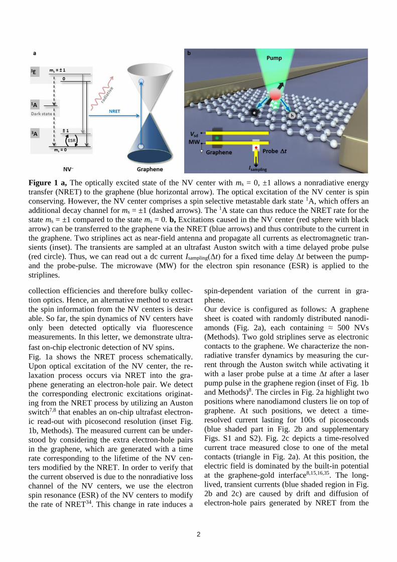
fast on-chip electronic detection of NV spins. Fig. 1a shows the NRET process schematically.
Upon optical excitation of the NV center, the re-
laxation process occurs via NRET into the gra-
phene generating an electron-hole pair. We detect
the corresponding electronic excitations originat-
ing from the NRET process by utilizing an Auston
switch7,8 that enables an on-chip ultrafast electron-
ic read-out with picosecond resolution (inset Fig.
1b, Methods). The measured current can be under-
stood by considering the extra electron-hole pairs
in the graphene, which are generated with a time
rate corresponding to the lifetime of the NV cen-
ters modified by the NRET. In order to verify that
the current observed is due to the nonradiative loss
channel of the NV centers, we use the electron
spin resonance (ESR) of the NV centers to modify
the rate of NRET34. This change in rate induces a
spin-dependent variation of the current in gra-
phene.
Our device is configured as follows: A graphene
sheet is coated with randomly distributed nanodi-
amonds (Fig. 2a), each containing ≈ 500 NVs
(Methods). Two gold striplines serve as electronic
contacts to the graphene. We characterize the non-
radiative transfer dynamics by measuring the cur-
rent through the Auston switch while activating it
with a laser probe pulse at a time Δt after a laser
pump pulse in the graphene region (inset of Fig. 1b
and Methods)8. The circles in Fig. 2a highlight two
positions where nanodiamond clusters lie on top of
graphene. At such positions, we detect a time-
resolved current lasting for 100s of picoseconds
(blue shaded part in Fig. 2b and supplementary
Figs. S1 and S2). Fig. 2c depicts a time-resolved
current trace measured close to one of the metal
contacts (triangle in Fig. 2a). At this position, the
electric field is dominated by the built-in potential
at the graphene-gold interface8,15,16,35. The long-
lived, transient currents (blue shaded region in Fig.
2b and 2c) are caused by drift and diffusion of
electron-hole pairs generated by NRET from the
Figure 1 a, The optically excited state of the NV center with ms = 0, ±1 allows a nonradiative energy
transfer (NRET) to the graphene (blue horizontal arrow). The optical excitation of the NV center is spin
conserving. However, the NV center comprises a spin selective metastable dark state 1A, which offers an
additional decay channel for ms = ±1 (dashed arrows). The 1A state can thus reduce the NRET rate for the
state ms = ±1 compared to the state ms = 0. b, Excitations caused in the NV center (red sphere with black
arrow) can be transferred to the graphene via the NRET (blue arrows) and thus contribute to the current in
the graphene. Two striplines act as near-field antenna and propagate all currents as electromagnetic tran-
sients (inset). The transients are sampled at an ultrafast Auston switch with a time delayed probe pulse
(red circle). Thus, we can read out a dc current Isampling(Δt) for a fixed time delay Δt between the pump-
and the probe-pulse. The microwave (MW) for the electron spin resonance (ESR) is applied to the
striplines.

3
NV centers and by direct optical absorption within
the graphene. The excited electron-hole pairs di-
rectly generate a photoresponse11 or decay into hot
electrons and generate a photoresponse by the
Seebeck effect36. The first peak at a time delay of
Δt ≈ 0 ps corresponds to an ultrafast displacement
current within the graphene; i.e. the screening of
the local electric field caused by photogenerated
charge carriers7,8. For each position, we plot the
long-lived, transient currents for increasing time
frames (Figs. 2d, 2e, and 2f). We detect such long-
lived currents at positions where clusters of
nanodiamonds are located (e.g. circles and trian-
gle). The long-lived currents have a timescale be-
tween picoseconds up to nanoseconds, which ex-
ceeds the direct laser generated carrier dynamics in
pristine graphene8,15,16,35 (supplementary Fig. S3).
In addition, the measured decay time is significant-
ly shorter than the natural, characteristic lifetime
of NV centers21. Therefore, these are signatures
that the long-lived currents comprise the nonradia-
tive transfer dynamics.
In order to verify that that the long-lived contribu-
tions to Isampling stem from charge carriers from the
NRET process, instead from direct laser light ab-
sorption, ESR provides a selective tool. To this
end, we apply a microwave signal to the striplines
(inset of Fig. 1b and Methods). The corresponding
oscillating magnetic field can be tuned to the spin
splitting energy of the NV centers with a reso-
nance at fMW = 2.875 GHz (ESR in Fig. 1a)22. The
energy spectrum of the NV center contains a spin
triplet system with a ms = 0 state and ms = ±1 de-
generated states. Upon laser excitation the spin
state of the system is conserved21. If the NV center
was in the ms = 0 excited state, it decays radiative-
ly with a characteristic lifetime of 10 ns to the ms =
0 ground state. Conversely, if the NV center was in
the excited state ms = ±1, it decays via a dark state
to the ground state ms = 0 (Fig. 1a)21. The dark
state has a lifetime in the order of hundreds of ns.
This difference in decay rates between the ms = 0
and ms = ±1 excited states is mapped via NRET
onto the graphene by the creation of an electron-
hole pair with corresponding probability.
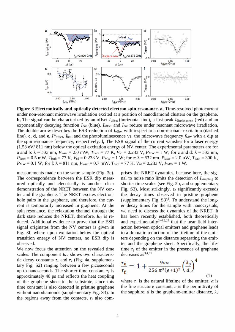
Fig. 3a and 3b show Isampling for non-resonant and
resonant ESR conditions. For analysis, we fit the
data with three contributions: a baseline Ioffset, a
Gaussian immediate response Idisplacement (red line)
and an exponentially decaying function Ihot (blue
line and supplementary Fig. S2). Ihot describes the
long-lived currents. We find that both Ioffset and Ihot
reduce under the spin resonance conditions, while
Idisplacement stays constant. The latter means that the
local electric field at this position within the gra-
phene and the displacement of the field are neither
altered by the NRET nor the microwaves. The
component Ihot comprises transfer processes with a
time-scale of several picoseconds, while Ioffset cor-
responds to a time-scale of ≈ 13 ns (the inverse of
the repetition frequency of the laser 76 MHz).
When this offset component is plotted vs. micro-
wave frequency and aliases of the laser-repetition
are subtracted (supplementary information), the
resulting I*offset exhibits a clear dip at the ESR fre-
quency (Fig. 3c and supplementary Fig. S4) which
is also observed for the component Ihot of the cur-
rent (Fig. 3d). This is consistent with standard ESR
frequency-dependent photoluminescence
Figure 2 Ultrafast electronic read-out of NV
centers. a, Graphene (in-between the white vertical
lines) with diamond nanocrystals on top. Two met-
al striplines (yellow) act as source-drain contacts.
Scale bar, 10 µm. b, and c, Time-resolved current
Isampling at positions marked by dashed circle and a
triangle in Fig. 2a, respectively. d, e, and f, Color
maps of the averaged long-lived currents as high-
lighted by blue areas in Figs. 2b and 2c for time
intervals of Δt for (10 – 50) ps (2d), (10 – 250) ps
(2e), and (10 – 450) ps (2f). Experimental parame-
ters are 77 K, Plaser = 3.0 mW, Vsd = 0 V.
4
measurements made on the same sample (Fig. 3e).
The correspondence between the ESR dip meas-
ured optically and electrically is another clear
demonstration of the NRET between the NV cen-
ter and the graphene. The NRET excites electron-
hole pairs in the graphene, and therefore, the cur-
rent is temporarily increased in graphene. At the
spin resonance, the relaxation channel through the
dark state reduces the NRET, therefore, Ihot is re-
duced. Additional evidence to prove that the ESR
signal originates from the NV centers is given in
Fig. 3f, where upon excitation below the optical
transition energy of NV centers, no ESR dip is
observed.
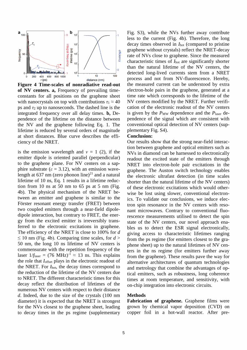
We now focus the attention on the revealed time
scales. The component Ihot shows two characteris-
tic decay constants τ1 and τ2 (Fig. 4a, supplemen-
tary Fig. S2) ranging between a few picoseconds
up to nanoseconds. The shorter time constant τ1 is
approximately 40 ps and reflects the heat coupling
of the graphene sheet to the substrate, since this
time constant is also detected in pristine graphene
without nanodiamonds (supplementary Fig. S3). In
the regions away from the contacts, τ1 also com-
prises the NRET dynamics, because here, the sig-
nal to noise ratio limits the detection of Isampling to
shorter time scales (see Fig. 2b, and supplementary
Fig. S3). Most strikingly, τ2 significantly exceeds
the decay times observed in pristine graphene
(supplementary Fig. S3)8. To understand the long-
er decay times for the sample with nanocrystals,
we need to discuss the dynamics of the NRET. It
has been recently established, both theoretically
and experimentally2–4,6,19 that the near field inter-
action between optical emitters and graphene leads
to a dramatic reduction of the lifetime of the emit-
ters depending on the distance separating the emit-
ter and the graphene sheet. Specifically, the life-
time τg of the emitter in the presence of graphene
decreases as3,4,19
(1)
where τ0 is the natural lifetime of the emitter, α is
the fine structure constant, ε is the permittivity of
the sapphire, d is the graphene-emitter distance, λ0
Figure 3 Electronically and optically detected electron spin resonance. a, Time-resolved photocurrent
under non-resonant microwave irradiation excited at a position of nanodiamond clusters on the graphene.
b, The signal can be characterized by an offset Ioffset (horizontal line), a fast peak Idisplacement (red) and an
exponentially decaying function Ihot (blue). Ioffset and Ihot reduce under resonant microwave irradiation.
The double arrow describes the ESR-reduction of Ioffset with respect to a non-resonant excitation (dashed
line). c, d, and e, I*offset, Ihot, and the photoluminescence vs. the microwave frequency fMW with a dip at
the spin resonance frequency, respectively. f, The ESR signal of the current vanishes for a laser energy
(1.53 eV/ 811 nm) below the optical excitation energy of NV center. The experimental parameters are for
a and b: λ = 535 nm, Plaser = 2.0 mW, Tbath = 77 K, Vsd = 0.233 V, PMW = 1 W; for c and d: λ = 535 nm,
Plaser = 0.5 mW, Tbath = 77 K, Vsd = 0.233 V, PMW = 1 W; for e: λ = 532 nm, Plaser = 2.0 µW, Tbath = 300 K,
PMW = 0.1 W; for f: λ = 811 nm, Plaser = 0.7 mW, Tbath = 77 K, Vsd = 0.233 V, PMW = 1 W.
5
Figure 4 Time-scales of nonradiative read-out
of NV centers. a, Frequency of prevailing time-
constants for all positions on the graphene sheet
with nanocrystals on top with contributions τ1 ≈ 40
ps and τ2 up to nanoseconds. The dashed line is the
integrated frequency over all delay times. b, De-
pendence of the lifetime on the distance between
the NV and the graphene following Eq. 1. The
lifetime is reduced by several orders of magnitude
at short distances. Blue curve describes the effi-
ciency of the NRET.
is the emission wavelength and ν = 1 (2), if the
emitter dipole is oriented parallel (perpendicular)
to the graphene plane. For NV centers on a sap-
phire substrate (ε = 3.12), with an emission wave-
length at 637 nm (zero phonon line)21 and a natural
lifetime of 10 ns, Eq. 1 results in a lifetime reduc-
tion from 10 ns at 50 nm to 65 ps at 5 nm (Fig.
4b). The physical mechanism of the NRET be-
tween an emitter and graphene is similar to the
Förster resonant energy transfer (FRET) between
two coupled emitters through a near-field dipole-
dipole interaction, but contrary to FRET, the ener-
gy from the excited emitter is irreversibly trans-
ferred to the electronic excitations in graphene.
The efficiency of the NRET is close to 100% for d
≤ 10 nm (Fig. 4b). Comparing time scales, for d >
50 nm, the long 10 ns lifetime of NV centers is
commensurate with the repetition frequency of the
laser 1/flaser = (76 MHz)-1 ≈ 13 ns. This explains
the role that Ioffset plays in the electronic readout of
the NRET. For Ihot, the decay times correspond to
the reduction of the lifetime of the NV centers due
to NRET. The different characteristic times for this
decay reflect the distribution of lifetimes of the
numerous NV centers with respect to their distance
d. Indeed, due to the size of the crystals (100 nm
diameter) it is expected that the NRET is strongest
for the NVs closest to the graphene sheet, leading
to decay times in the ps regime (supplementary
Fig. S3), while the NVs further away contribute
less to the current (Fig. 4b). Therefore, the long
decay times observed in Ihot (compared to pristine
graphene without crystals) reflect the NRET-decay
rate of NVs close to graphene. Since the measured
characteristic times of Ihot are significantly shorter
than the natural lifetime of the NV centers, the
detected long-lived currents stem from a NRET
process and not from NV-fluorescence. Hereby,
the measured current can be understood by extra
electron-hole pairs in the graphene, generated at a
time rate which corresponds to the lifetime of the
NV centers modified by the NRET. Further verifi-
cation of the electronic readout of the NV centers
is given by the PMW dependence and the Plaser de-
pendence of the signal which are consistent with
conventional optical detection of NV centers (sup-
plementary Fig. S4).
Conclusion:
Our results show that the strong near-field interac-
tion between graphene and optical emitters such as
NVs in diamond can be harnessed to electronically
readout the excited state of the emitters through
NRET into electron-hole pair excitations in the
graphene. The Auston switch technology enables
the electronic ultrafast detection (in time scales
shorter than the natural lifetime of the NV centers)
of these electronic excitations which would other-
wise be lost using slower, conventional electron-
ics. To validate our conclusions, we induce elec-
tron spin resonance in the NV centers with reso-
nant microwaves. Contrary to conventional fluo-
rescence measurements utilised to detect the spin
state of the NV centers, our novel approach ena-
bles us to detect the ESR signal electronically,
giving access to characteristic lifetimes ranging
from the ps regime (for emitters closest to the gra-
phene sheet) up to the natural lifetimes of NV cen-
ters in the ns regime (for emitters further away
from the graphene). These results pave the way for
alternative architectures of quantum technologies
and metrology that combine the advantages of op-
tical emitters, such as robustness, long coherence
times at room temperature, and sensitivity, with
on-chip integration into electronic circuits.
Methods Fabrication of graphene. Graphene films were
grown by chemical vapor deposition (CVD) on
copper foil in a hot-wall reactor. After pre-
6
annealing the copper foil at 1000°C under a flow
of 28 sccm H2 for 40 min, graphene was grown for
30 min under a flow of 3.5 sccm CH4 and 16 sccm
H2 at a total pressure of 10 mbar. Then, the cop-
per-graphene foil was cooled to room temperature
under growth atmosphere. For transfer, samples
were spin-coated with poly(methylmethacrylate)
(PMMA) and floated on 0.5 M aqueous FeCl3 so-
lution overnight. After complete dissolution of the
copper foil, the films were rinsed with deionized
water and transferred to the pre-structured sapphire
substrates with a stripline circuit on top.
Design of the stripline circuit. Sapphire with a
thickness of 430 µm, covered with a 300 nm thick
silicon layer, is used as a substrate. The silicon is
implanted with O2 ions to yield an excess carrier
lifetime of ≈ 1 ps. The silicon is etched in a first
lithographic step to define the ultra-fast photo
switch (Auston switch), using HF/ HNO3 as etch-
ant. Ti (5 nm) and Au (25 nm) are evaporated to
form the striplines and the readout contact of the
Auston switch. The two striplines are 15 µm dis-
tanced and they have a width of 5 µm. Each
stripline has a total length of about 4.4 cm. The
graphene is deposited on top of the striplines and
defined to a 25 µm wide stripe in a last lithograph-
ic step by using O2 plasma to remove the spare
graphene. The distance between the graphene and
the Auston switch is ≈ 250 µm. The nanodiamonds
have a diameter of ≈ 100 nm and each comprises ≈
500 NVs (Adamas Nanotechnologies, Inc., Ra-
leigh, NC 27617). They are spin-coated onto the
circuit from a propanol solution.
On chip, time-domain THz spectroscopy. A
pulsed titanium:sapphire laser (repetition rate 76
MHz, pulse length 160 fs), operated at 811 nm, is
used for the probe-pulse of the time-resolved
measurements. The light is additionally converted
by a non-linear fibre to a wavelength of λ = (535 ±
5) nm, and focused as the pump-laser onto the gra-
phene with a 10x objective. Each pump-laser pulse
excites both graphene and the NV centers. The
ultrafast currents in the graphene-sheet are collect-
ed by the striplines. Consequently an electromag-
netic transient, which is proportional to the initial
current, will propagate along the striplines. After a
certain time delay Δt, the probe-pulse triggers the
Auston-switch and the presence of the electromag-
netic transient drives an electric current, which
decays within 1 ps. This current is read out as Isam-
pling(Δt) and it is proportional to the electric field of
the propagating electromagnetic transient. The
moment, when the pump-pulse hits the graphene,
defines Δt ≈ 0 ps. Both laser beams are focused
through the same objective on the sample, but the
position of the pump beam on the graphene-sheet
can be independently scanned by a motorized mir-
ror. The spot size of the pump beam is 3- 4 µm.
This beam has a power of Plaser = 0.3- 3 mW. The
probe laser power is set to 100 mW. All laser pow-
ers are measured in front of the objective. We use
a dual frequency modulation of the pump- and the
probe-beam, and read out the pre-amplified elec-
tric current Isampling with a lock-in amplifier. The
striplines are either connected to a voltage source
(Vsd) or connected via a bias tee to both an ampli-
fied microwave source with power PMW and the
voltage source for electron spin resonance (ESR)
experiments. All measurements are done in vacu-
um (10-5 mbar) at Tbath = 77 K.
References 1. Ford, G. W. & Weber, W. H. Electromagnetic in-
teractions of molecules with metal surfaces, Phys. Rep.
113, 195–287 (1984).
2. Gómez-Santos, G. & Stauber, T. Fluorescence
quenching in graphene: a fundamental ruler and evi-
dence for transverse plasmons, Phys. Rev. B 84, 165438
(2011).
3. Gaudreau, L. et al. Universal distance-scaling of
nonradiative energy transfer to graphene, Nano Lett.
13, 2030–2035 (2013).
4. Swathi, R. S. & Sebastian, K. L. Long range reso-
nance energy transfer from a dye molecule to graphene
has (distance)-4 dependence, J. Chem. Phys. 130, 86101
(2009).
5. Velizhanin, K. A. & Shahbazyan, T. V. Long-range
plasmon-assisted energy transfer over doped graphene,
Phys. Rev. B 86, 245432 (2012).
6. Koppens, F. H. L., Chang, D. E. & Garcia de Aba-
jo, J. F. Graphene plasmonics: a platform for strong
light–matter interactions, Nano Lett. 11, 3370–3377
(2011).
7. Auston, D. H. Impulse response of photoconductors
in transmission lines, IEEE J. Quant. Electron. 19,
639–648 (1983).
8. Prechtel, L. et al. Time-resolved ultrafast photocur-
rents and terahertz generation in freely suspended gra-
phene, Nat. Commun. 3 (2012).
9. Bonaccorso, F., Sun, Z., Hasan, T. & Ferrari, A. C.
Graphene photonics and optoelectronics, Nature Pho-
ton. 4, 611–622 (2010).
7
10. Mayorov, A. S. et al. Micrometer-scale ballistic
transport in encapsulated graphene at room tempera-
ture, Nano Lett. 11, 2396–2399 (2011).
11. Xia, F., Mueller, T., Lin, Y.-m., Valdes-Garcia, A.
& Avouris, P. Ultrafast graphene photodetector, Nature
Nanotech. 4, 839–843 (2009).
12. Xu, X., Gabor, N. M., Alden, J. S., van der Zande,
Arend M. & McEuen, P. L. Photo-thermoelectric effect
at a graphene interface junction, Nano Lett. 10, 562–
566 (2010).
13. Gabor, N. M. et al. Hot carrier-assisted intrinsic
photoresponse in graphene, Science 334, 648–652
(2011).
14. Song, J. C. W., Rudner, M. S., Marcus, C. M. &
Levitov, L. S. Hot carrier transport and photocurrent
response in graphene, Nano Lett. 11, 4688–4692
(2011).
15. Sundaram, R. S. et al. The graphene–gold interface
and its implications for nanoelectronics, Nano Lett. 11,
3833–3837 (2011).
16. Sun, D. et al. Ultrafast hot-carrier-dominated pho-
tocurrent in graphene, Nature Nanotech. 7, 114–118
(2012).
17. Freitag, M., Low, T. & Avouris, P. Increased re-
sponsivity of suspended graphene photodetectors, Nano
Lett. 13, 1644–1648 (2013).
18. Chen, Z., Berciaud, S., Nuckolls, C., Heinz, T. F. &
Brus, L. E. Energy transfer from individual semicon-
ductor nanocrystals to graphene, ACS Nano 4, 2964–
2968 (2010).
19. Tisler, J. et al. Single defect center scanning near-
field optical microscopy on graphene, Nano Lett. 13,
3152–3156 (2013).
20. Stöhr, R. J. et al. Super-resolution fluorescence
quenching microscopy of graphene, ACS Nano 6,
9175–9181 (2012).
21. Jelezko, F. & Wrachtrup, J. Single defect centres in
diamond: a review, Phys. Status Solidi A 203, 3207–
3225 (2006).
22. Jelezko, F., Gaebel, T., Popa, I., Gruber, A. &
Wrachtrup, J. Observation of coherent oscillations in a
single electron spin, Phys. Rev. Lett. 92, 76401 (2004).
23. Dutt, M. V. G. et al. Quantum register based on
individual electronic and nuclear spin qubits in dia-
mond, Science 316, 1312–1316 (2007).
24. Neumann, P. et al. Multipartite entanglement
among single spins in diamond, Science 320, 1326–
1329 (2008).
25. Fuchs, G. D., Burkard, G., Klimov, P. V. & Aws-
chalom, D. D. A quantum memory intrinsic to single
nitrogen–vacancy centres in diamond, Nat. Phys. 7,
789–793 (2011).
26. Pfaff, W. et al. Demonstration of entanglement-by-
measurement of solid-state qubits, Nat. Phys. 9, 29–33
(2012).
27. Bernien, H. et al. Heralded entanglement between
solid-state qubits separated by three metres, Nature
497, 86–90 (2013).
28. Togan, E. et al. Quantum entanglement between an
optical photon and a solid-state spin qubit, Nature 466,
730–734 (2010).
29. Kurtsiefer, C., Mayer, S., Zarda, P. & Weinfurter,
H. Stable solid-state source of single photons, Phys.
Rev. Lett. 85, 290–293 (2000).
30. Maze, J. R. et al. Nanoscale magnetic sensing with
an individual electronic spin in diamond, Nature 455,
644–647 (2008).
31. Acosta, V. M. et al. Temperature dependence of the
nitrogen-vacancy magnetic resonance in diamond,
Phys. Rev. Lett. 104, 70801 (2010).
32. Plakhotnik, T. & Gruber, D. Luminescence of ni-
trogen-vacancy centers in nanodiamonds at tempera-
tures between 300 and 700 K: perspectives on nan-
othermometry, Phys. Chem. Chem. Phys. 12, 9751–
9756 (2010).
33. Toyli, D. M., de las Casas, C. F., Christle, D. J.,
Dobrovitski, V. V. & Awschalom, D. D. Fluorescence
thermometry enhanced by the quantum coherence of
single spins in diamond, Proc. Natl. Acad. Sci. U.S.A.
110, 8417–8421 (2013).
34. Gruber, A. Scanning confocal optical microscopy
and magnetic resonance on single defect centers, Sci-
ence 276, 2012–2014 (1997).
35. Freitag, M., Low, T., Xia, F. & Avouris, P. Photo-
conductivity of biased graphene, Nature Photon. 7, 53–
59 (2012).
36. Lemme, M. C. et al. Gate-activated photoresponse
in a graphene p–n junction, Nano Lett. 11, 4134–4137
(2011).
Acknowledgements
We gratefully thank Antoine Reserbat-Plantey for
technical support. This work was supported by the
ERC Grant NanoREAL (n°306754) and the "Cen-
ter of NanoScience (CeNS)" in Munich. L.G.
acknowledges financial support from Marie-Curie
International Fellowship COFUND and ICFOnest
program. F.K. acknowledges support by the
Fundacio Cellex Barcelona, the ERC Career inte-
gration grant 294056 (GRANOP) and the ERC
starting grant 307806 (CarbonLight).
Author Contribution
A.B. and L.G. performed the experiments and ana-
lyzed the data together with A.W.H, F.K., M.S.,
J.A.G., M.S.B., H.H., and H.K.. F.K. and A.W.H.
conceived the study. All authors co-wrote the pa-
per.
1
Supplementary Information
Ultrafast electronic detection of diamond NV centers coupled to graphene
Andreas Brenneis, Louis Gaudreau, Max Seifert, Helmut Karl, Martin S. Brandt, Hans Huebl, Jose A. Garrido,
Frank H.L. Koppens*, Alexander W. Holleitner*
Supplementary Notes
1. Ultrafast time-resolved photocurrents in graphene with nanocrystals on top:
The NRET generates additional electron-hole pairs in the graphene at a time-constant which corresponds
to the lifetime of the NV centers modified by the NRET. The dynamics of the additional electron-hole
pairs in graphene are governed by the same physical mechanisms as of hot, photo-excited electron-hole
pairs. Such photocurrents are actively discussed either in terms of the so-called photothermoelectric effect 8,13–14,16 or built-in electric fields created by the different work function mismatches between the different
materials (diamond-graphene, metal-graphene)8,15,16,36. In the following, we characterize the NRET-
currents in detail.
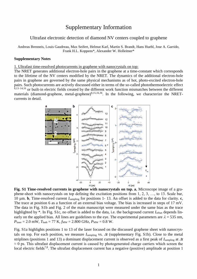
Fig. S1 Time-resolved currents in graphene with nanocrystals on top. a, Microscope image of a gra-
phene-sheet with nanocrystals on top defining the excitation positions from 1, 2, 3, …, to 13. Scale bar,
10 µm. b, Time-resolved current Isampling for positions 1- 13. An offset is added to the data for clarity. c,
The trace at position 6 as a function of an external bias voltage. The bias is increased in steps of 17 mV.
The data in Fig. S1b and Fig. 2 of the main manuscript were measured under the same bias as the trace
highlighted by *. In Fig. S1c, no offset is added to the data, i.e. the background current Ioffset depends lin-
early on the applied bias. All lines are guidelines to the eye. The experimental parameters are = 535 nm,
Plaser = 2.0 mW, Tbath = 77 K, fMW = 2.800 GHz, PMW = 0.8 W.
Fig. S1a highlights positions 1 to 13 of the laser focused on the discussed graphene sheet with nanocrys-
tals on top. For each position, we measure Isampling vs. t (supplementary Fig. S1b). Close to the metal
striplines (positions 1 and 13) a dominant displacement current is observed as a first peak of Isampling at t
≈ 0 ps. This ultrafast displacement current is caused by photogenerated charge carriers which screen the
local electric fields7,8. The ultrafast displacement current has a negative (positive) amplitude at position 1
2
(position 13) consistent with the direction of the local built-in electric fields at the metal-graphene (gra-
phene-metal)-interface8. The displacement current is sensitive to built-in potentials caused by the work
function difference of graphene and the metal. From position 1 to 13 Isampling comprises a rich structure
and the ultrafast displacement current at t ≈ 0 ps changes the sign twice. The behavior of the displace-
ment current can be explained by the presence of local electric fields caused by the different work func-
tions of graphene and the diamond nanocrystals. We prove this by the application of an external bias volt-
age and, therefore, a macroscopic electric field which flattens the local field distribution. To this end, the
trace at position 6 is highlighted in blue in Fig. S1b. When an external bias is applied (supplementary Fig.
S1c), the displacement peak at t ≈ 0 ps changes sign according to the bias voltage. In other words, for
positions far away from the contacts, one needs an external electric field to observe and enhance a time-
resolved photocurrent. We note that at the positions of the nanocrystals and for a finite bias voltage, we
also observe the long-lived photocurrents of Isampling (Fig. 2 of the main manuscript), as discussed in the
next section.
2. Comparison of the time-resolved, long-lived photocurrents with and without NVs:
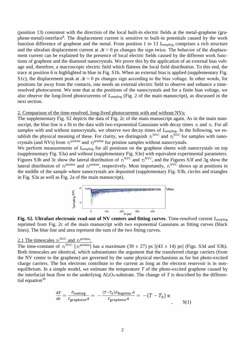
The supplementary Fig. S2 depicts the data of Fig. 2c of the main manuscript again. As in the main man-
uscript, the blue line is a fit to the data with two exponential Gaussians with decay times 1 and 2. For all
samples with and without nanocrystals, we observe two decay times of Isampling. In the following, we es-
tablish the physical meaning of these. For clarity, we distinguish 1NVC and 2
NVC for samples with nano-
crystals (and NVs) from 1pristine and 2
pristine for pristine samples without nanocrystals.
We perform measurements of Isampling for all positions on the graphene sheets with nanocrystals on top
(supplementary Fig. S3a) and without (supplementary Fig. S3e) with equivalent experimental parameters.
Figures S3b and 3c show the lateral distribution of 1NVC and 2
NVC, and the Figures S3f and 3g show the
lateral distribution of 1pristine and 2
pristine, respectively. Most importantly, 1NVC shows up at positions in
the middle of the sample where nanocrystals are deposited (supplementary Fig. S3b, circles and triangles
in Fig. S3a as well as Fig. 2a of the main manuscript).
Fig. S2. Ultrafast electronic read-out of NV centers and fitting curves. Time-resolved current Isampling
reprinted from Fig. 2c of the main manuscript with two exponential Gaussians as fitting curves (black
lines). The blue line and area represent the sum of the two fitting curves.
2.1 The timescales 1NVC and 1
pristine:
The time-constant of 1NVC [1
pristine] has a maximum (39 ± 27) ps [(43 ± 14) ps] (Figs. S3d and S3h).
Both timescales are identical, which substantiates the argument that the transferred charge carriers (from
the NV center to the graphene) are governed by the same physical mechanisms as for hot photo-excited
charge carriers. The hot electrons contribute to the current as long as the electron reservoir is in non-
equilibrium. In a simple model, we estimate the temperature T of the photo-excited graphene caused by
the interfacial heat flow to the underlying Al2O3-substrate. The change of T is described by the differen-
tial equation39
S(1)
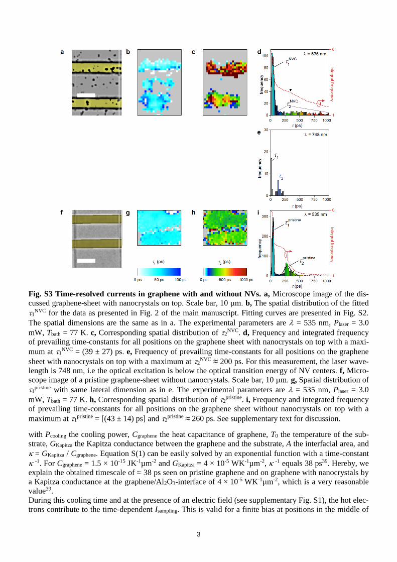
3
Fig. S3 Time-resolved currents in graphene with and without NVs. a, Microscope image of the dis-
cussed graphene-sheet with nanocrystals on top. Scale bar, 10 µm. b, The spatial distribution of the fitted
1NVC for the data as presented in Fig. 2 of the main manuscript. Fitting curves are presented in Fig. S2.
The spatial dimensions are the same as in a. The experimental parameters are = 535 nm, Plaser = 3.0
mW, Tbath = 77 K. c, Corresponding spatial distribution of 2NVC. d, Frequency and integrated frequency
of prevailing time-constants for all positions on the graphene sheet with nanocrystals on top with a maxi-
mum at 1NVC = (39 ± 27) ps. e, Frequency of prevailing time-constants for all positions on the graphene
sheet with nanocrystals on top with a maximum at 2NVC ≈ 200 ps. For this measurement, the laser wave-
length is 748 nm, i.e the optical excitation is below the optical transition energy of NV centers. f, Micro-
scope image of a pristine graphene-sheet without nanocrystals. Scale bar, 10 µm. g, Spatial distribution of
1pristine with same lateral dimension as in e. The experimental parameters are = 535 nm, Plaser = 3.0
mW, Tbath = 77 K. h, Corresponding spatial distribution of 2pristine. i, Frequency and integrated frequency
of prevailing time-constants for all positions on the graphene sheet without nanocrystals on top with a
maximum at 1pristine = [(43 ± 14) ps] and 2
pristine ≈ 260 ps. See supplementary text for discussion.
with Pcooling the cooling power, Cgraphene the heat capacitance of graphene, T0 the temperature of the sub-
strate, GKapitza the Kapitza conductance between the graphene and the substrate, A the interfacial area, and
= GKapitza / Cgraphene. Equation S(1) can be easily solved by an exponential function with a time-constant
-1. For Cgraphene = 1.5 × 10⁻¹⁵ JK-1µm-2 and GKapitza = 4 × 10⁻⁵ WK-1µm-2, -1 equals 38 ps39. Hereby, we
explain the obtained timescale of ≈ 38 ps seen on pristine graphene and on graphene with nanocrystals by
a Kapitza conductance at the graphene/Al2O3-interface of 4 × 10⁻⁵ WK-1µm-2, which is a very reasonable
value39.
During this cooling time and at the presence of an electric field (see supplementary Fig. S1), the hot elec-
trons contribute to the time-dependent Isampling. This is valid for a finite bias at positions in the middle of
4
the sample where nanocrystals are deposited (circles and triangles in supplementary Fig. S3a and Fig. 2a
of the main manuscript), and independent of the bias, at the metal contacts where built-in electric fields
give rise to the electric field (supplementary Figs. S3b and S3f).
2.2 The timescales 2pristineand 2
NVC:
Y. K. Koh et al. demonstrated that a lateral heat flow within graphene is only dominant for a lateral dis-
tance of ≈ 180 nm to the metal striplines40. On the other hand, the phonon temperature of the metal
striplines decays on a timescale of hundreds of picoseconds through transverse heat diffusion and cou-
pling to the substrate41,42. In turn, there are hot electrons in the vicinity of the metal-graphene interface,
and Isampling shows a decaying component close to the metal contact.
Supplementary Fig. S3h demonstrates that 2pristine ≈ 260 ps, and Fig. S3g verifies that 2
pristine is rather
homogeneous along the metal-graphene interfaces. Both results corroborate the interpretation of an addi-
tional heat-sink caused by the metal contacts. We point out that this interpretation is consistent with inde-
pendent measurements on freely suspended, pristine graphene, in which we observed an exponential
timescale in the range of 100 to 300 ps at the graphene-metal interface8.
Intriguingly, 2NVC shows longer timescales up to nanoseconds (supplementary Fig. S3d), and the lateral
distribution of 2NVC is less homogeneous (supplementary Fig. S3c). We still detect a tiny bump in the
integrated frequency for 2NVC (triangle in supplementary Fig. S3d), which we tentatively interpret to be a
reminiscence of the lateral heat flow to the metal contacts. However, there is a dominating NRET-process
with distinctively longer 2NVC in close vicinity of the metal striplines (supplementary Fig. S3c). The vi-
cinity to the striplines helps to measure 2NVC. There, the strong static interfacial built-in electric fields
make the hot electrons propagate; independent of the time-delay to the pump-pulse.
To conclude this section, time-constants exceeding ≈ 260 ps are only seen for graphene with nanocrystals
on top, and they are significantly shorter than the natural, characteristic lifetime of NV centers without the
NRET. Since the corresponding currents can be controlled by an electron spin resonance, the underlying
processes are related to the optically excited spins in the NV centers; proving the interpretation of a non-
radiative energy transfer from the NV centers to the graphene.
3. Electron Spin Resonance (ESR) Measurements:
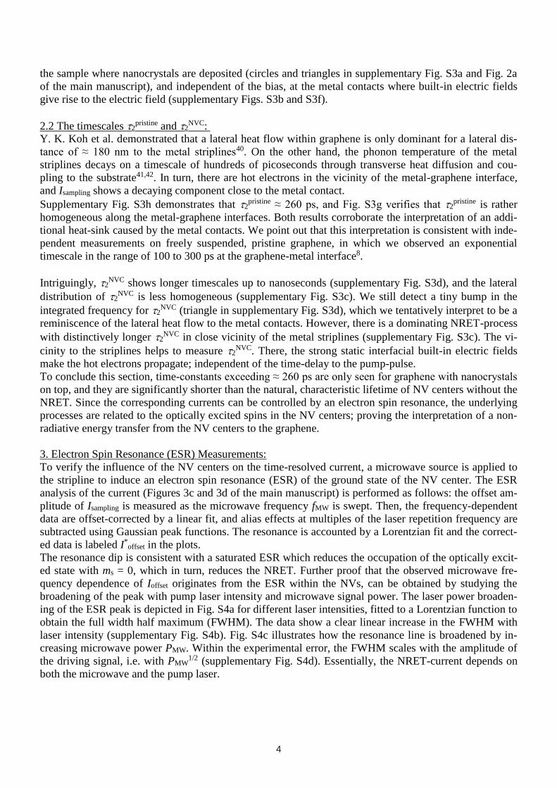
To verify the influence of the NV centers on the time-resolved current, a microwave source is applied to
the stripline to induce an electron spin resonance (ESR) of the ground state of the NV center. The ESR
analysis of the current (Figures 3c and 3d of the main manuscript) is performed as follows: the offset am-
plitude of Isampling is measured as the microwave frequency fMW is swept. Then, the frequency-dependent
data are offset-corrected by a linear fit, and alias effects at multiples of the laser repetition frequency are
subtracted using Gaussian peak functions. The resonance is accounted by a Lorentzian fit and the correct-
ed data is labeled I*offset in the plots.
The resonance dip is consistent with a saturated ESR which reduces the occupation of the optically excit-
ed state with ms = 0, which in turn, reduces the NRET. Further proof that the observed microwave fre-
quency dependence of Ioffset originates from the ESR within the NVs, can be obtained by studying the
broadening of the peak with pump laser intensity and microwave signal power. The laser power broaden-
ing of the ESR peak is depicted in Fig. S4a for different laser intensities, fitted to a Lorentzian function to
obtain the full width half maximum (FWHM). The data show a clear linear increase in the FWHM with
laser intensity (supplementary Fig. S4b). Fig. S4c illustrates how the resonance line is broadened by in-
creasing microwave power PMW. Within the experimental error, the FWHM scales with the amplitude of
the driving signal, i.e. with PMW1/2 (supplementary Fig. S4d). Essentially, the NRET-current depends on
both the microwave and the pump laser.

5
Fig. S4. Power dependence of ESR. a, Laser power dependence of I*offset vs. fMW with Lorentzian fitting
lines. b, Extracted FWHM vs. PLaser. Line is a linear fit. c, and d, microwave power dependence of I*offset
vs. fMW with fitting lines. The experimental parameters are = 535 nm, Tbath = 77 K, Vsd = 0 mV, (a,b)
PMW = 1 W, (c,d) Plaser = 2.0 mW e, The amplitude of the ultrafast photocurrent Ihot is reduced under reso-
nant microwave excitation (2.875 GHz) compared to the non-resonant excitation (2.800 GHz) for micro-
wave powers above 0.2 W measured at the position of the dotted circle in Fig. 2a. The experimental pa-
rameters are = 535 nm, Tbath = 77 K, Vsd = 0 mV, Plaser = 2.0 mW.
4. Power dependence of the ESR measured by Ihot:
Because the amplitude of the component Ihot is 0.3-0.4 pA at an overall noise floor of 0.1 pA, the detec-
tion of the ESR via Ihot with an ESR-dip of about 0.2 pA is inherently close to the experimental resolution
(compare Figs. 3a and 3b of the main manuscript). To still demonstrate the power dependence of the
ESR-dip also in Ihot, we measure Ihot for a non-resonant and resonant ESR-microwave-excitation. In the
supplementary Fig. S4e, the squares (circles) depict Ihot for fMW = 2.875 GHz (fMW = 2.800 GHz) vs. the
power of the applied microwave, which corresponds to a resonant (non-resonant) electron spin-excitation.
Within the experimental error, the power-dependent increase of the ESR-dip is clearly resolvable.
5. Correlation of the microscope image to PL intensity of the NV centers:
Fig. S5 shows the correlation of the microscope image (main manuscript Fig. 2a) to the photolumines-
cence intensity measured on the presented sample. For all positions of nanodiamond clusters on the sam-
ple (circles and triangle in Fig. 2a of the main manuscript) the observed PL emission correlates to the
black dots of the microscope image.

6
Fig. S5. Correlation of the microscope image to the photoluminescence intensity of the NV centers.
a, The nanodiamond clusters observed in the microscope image as black dots can be correlated to the
photoluminescence signal of the sample, presented in b,. The dotted circle denotes the excitation position
of Fig. 3a, and Fig. 3b. The triangle denotes the excitation position of Fig. 3d. The arrow indicates the
excitation position of Fig. 3c, Fig. 3e, and 3f of the main manuscript.
6. Photoluminescence spectrum of the NV centers:
Fig. S6 shows a PL spectrum taken at the position marked by the black arrow in Supplementary Fig. S5b.
The peaks at the zero phonon line (ZPL) of NV- and NV0 are highlighted.
Fig. S6. Photoluminescence spectrum of the NV centers. The spectrum is taken at the position marked
by the black arrow in Fig. S5 (excitation wavelength 532 nm, Plaser = 0.33 mW). Raw data is shown as
black line. A low pass filter (red line) is applied to remove the interference fringes that stem from reflec-
tions in the CCD detector. The zero phonon lines (ZPL) of the NV center and the Raman shift from the
sapphire substrate are marked in the spectrum.
7. NV PL lifetimes:
Fig. S7 shows a time resolved photoluminescence histogram for NV centers located on the sapphire sub-
strate and on the graphene, respectively. The data are fitted by two exponential Gaussians. On sapphire
and on graphene, we observe a component on the time scale of τb ≈ 10 ns, which is assigned to the life-
time of the radiative recombination. Only for NV centers located on the graphene, a fast component τa in
the order of hundreds of picoseconds is observed. This quenching is caused by an energy-transfer to the
graphene.

7
Fig. S7. Photoluminescence lifetimes of the NV centers. a, Time-resolved photoluminescence histo-
gram for NV centers located on the sapphire substrate and on the graphene. The data are fitted by two
exponential Gaussians (τa and τb, blue and black line, respectively). The instrument response function
(IRF) is shown as comparison. b, The component τ1 is faster for all positions on the graphene than on the
sapphire substrate.
References 39. Mak, K. F., Lui, C. H. & Heinz, T. F. Measurement of the thermal conductance of the gra-
phene/ SiO2 interface, Appl. Phys. Lett. 97, 221904 (2010).
40. Koh, Y. K., Bae, M.-H., Cahill, D. G. & Pop, E. Heat conduction across monolayer and few-layer graphenes, Nano Lett. 10, 4363–4368 (2010).
41. van Exter, M. & Lagendijk, A. Ultrashort surface-plasmon and phonon dynamics, Phys. Rev. Lett. 60, 49–52 (1988).
42. Paddock, C. A. & Eesley, G. L. Transient thermoreflectance from thin metal films, J. Appl. Phys. 60, 285–290 (1986).


![Preferential orientation of NV defects in CVD …Preferential orientation of NV defects in CVD diamond films grown on (113)-oriented substrates M. Lesik1, ... times [8]. Ultra-pure](https://img.pdfslide.net/doc/110x75/5e2c266a9540830fdc2ca58f/preferential-orientation-of-nv-defects-in-cvd-preferential-orientation-of-nv-defects.jpg)