Embed Size (px)
Citation preview
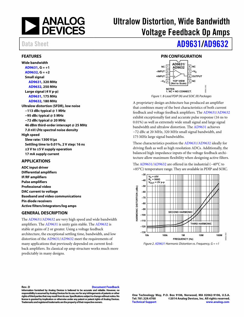
Ultralow Distortion, Wide BandwidthVoltage Feedback Op Amps
Data Sheet AD9631/AD9632
Rev. D Document Feedback Information furnished by Analog Devices is believed to be accurate and reliable. However, no responsibility is assumed by Analog Devices for its use, nor for any infringements of patents or other rights of third parties that may result from its use. Specifications subject to change without notice. No license is granted by implication or otherwise under any patent or patent rights of Analog Devices. Trademarks and registered trademarks are the property of their respective owners.
One Technology Way, P.O. Box 9106, Norwood, MA 02062-9106, U.S.A.Tel: 781.329.4700 ©2014 Analog Devices, Inc. All rights reserved. Technical Support www.analog.com
FEATURES Wide bandwidth
AD9631, G = +1 AD9632, G = +2 Small signal
AD9631, 320 MHz AD9632, 250 MHz
Large signal (4 V p-p) AD9631, 175 MHz AD9632, 180 MHz
Ultralow distortion (SFDR), low noise −113 dBc typical @ 1 MHz −95 dBc typical @ 5 MHz −72 dBc typical @ 20 MHz 46 dBm third-order intercept @ 25 MHz 7.0 nV/√Hz spectral noise density
High speed Slew rate: 1300 V/μs Settling time to 0.01%, 2 V step: 16 ns ±3 V to ±5 V supply operation 17 mA supply current
APPLICATIONS ADC input driver Differential amplifiers IF/RF amplifiers Pulse amplifiers Professional video DAC current to voltage Baseband and video communications Pin diode receivers Active filters/integrators/log amps
GENERAL DESCRIPTION The AD9631/AD9632 are very high speed and wide bandwidth amplifiers. The AD9631 is unity gain stable. The AD9632 is stable at gains of 2 or greater. Using a voltage feedback architecture, the exceptional settling time, bandwidth, and low distortion of the AD9631/AD9632 meet the requirements of many applications that previously depended on current feed-back amplifiers. Its classical op amp structure works much more predictably in many designs.
PIN CONFIGURATION
Figure 1. 8-Lead PDIP (N) and SOIC (R) Packages
A proprietary design architecture has produced an amplifier that combines many of the best characteristics of both current feedback and voltage feedback amplifiers. The AD9631/AD9632 exhibit exceptionally fast and accurate pulse response (16 ns to 0.01%) as well as extremely wide small signal and large signal bandwidth and ultralow distortion. The AD9631 achieves −72 dBc at 20 MHz, 320 MHz small signal bandwidth, and 175 MHz large signal bandwidths.
These characteristics position the AD9631/AD9632 ideally for driving flash as well as high resolution ADCs. Additionally, the balanced high impedance inputs of the voltage feedback archi-tecture allow maximum flexibility when designing active filters.
The AD9631/AD9632 are offered in the industrial (−40°C to +85°C) temperature range. They are available in PDIP and SOIC.
Figure 2. AD9631 Harmonic Distortion vs. Frequency, G = +1
1
2
3
4
NC
–INPUT
+INPUT
–VS
8
7
6
5
NCAD9631/AD9632
TOP VIEW(Not to Scale)
+VS
OUTPUT
NC
NOTES1. NC = NO CONNECT. 00
601-
001
–30
–40
–50
–60
–70
–80
–90
–100
–110
–120
–13010k 100k 1M 10M 100M
HA
RM
ON
IC D
IST
OR
TIO
N (
dB
c)
FREQUENCY (Hz)
THIRD HARMONIC
SECOND HARMONIC
VS = ±5VRL = 500ΩVOUT = 2V p-p
0060
1-00
2
AD9631/AD9632 Data Sheet
Rev. D | Page 2 of 20
TABLE OF CONTENTS Features .............................................................................................. 1 Applications ....................................................................................... 1 General Description ......................................................................... 1 Pin Configuration ............................................................................. 1 Revision History ............................................................................... 2 Specifications ..................................................................................... 3
Electrical Characteristics ............................................................. 3 Absolute Maximum Ratings ............................................................ 5
Metallization Photo ...................................................................... 5 Thermal Resistance ...................................................................... 5 Maximum Power Dissipation ..................................................... 5 ESD Caution .................................................................................. 5
Typical Performance Characteristics ............................................. 6 Theory of Operation ...................................................................... 15
General......................................................................................... 15 Feedback Resistor Choice.......................................................... 15 Pulse Response ........................................................................... 16 Large Signal Performance ......................................................... 16 Power Supply Bypassing ............................................................ 16 Driving Capacitive Loads .......................................................... 16
Applications Information .............................................................. 17 Operation as a Video Line Driver ............................................ 17 Active Filters ............................................................................... 17 Analog-to-Digital Converter (ADC) Driver .......................... 18 Layout Considerations ............................................................... 18
Outline Dimensions ....................................................................... 19 Ordering Guide .......................................................................... 20
REVISION HISTORY 2/14—Rev. C to Rev. D
Changes to Figure 33 ...................................................................... 10 Changes to Analog-to-Digital Converter (ADC) Driver Section and Figure 66 ................................................................................... 18 Updated Outline Dimensions ....................................................... 19 Changes to Ordering Guide .......................................................... 20
7/03—Rev. B to Rev. C
Deleted Evaluation Boards information .......................... Universal Deleted military CERDIP version .................................... Universal Change to Absolute Maximum Ratings ......................................... 3 Change to TPC 4 ............................................................................... 4 Change to TPC 10............................................................................. 5 Change to Figure 6 ......................................................................... 14 Updated Outline Dimensions ....................................................... 17
1/03—Rev. A to Rev. B
Deleted DIP (N) Inverter, SOIC (R) Inverter, and DIP (N) Noninverter Evaluation Boards in Figures 12–14 ...................... 17 Updated Outline Dimensions ....................................................... 18
Data Sheet AD9631/AD9632
Rev. D | Page 3 of 20
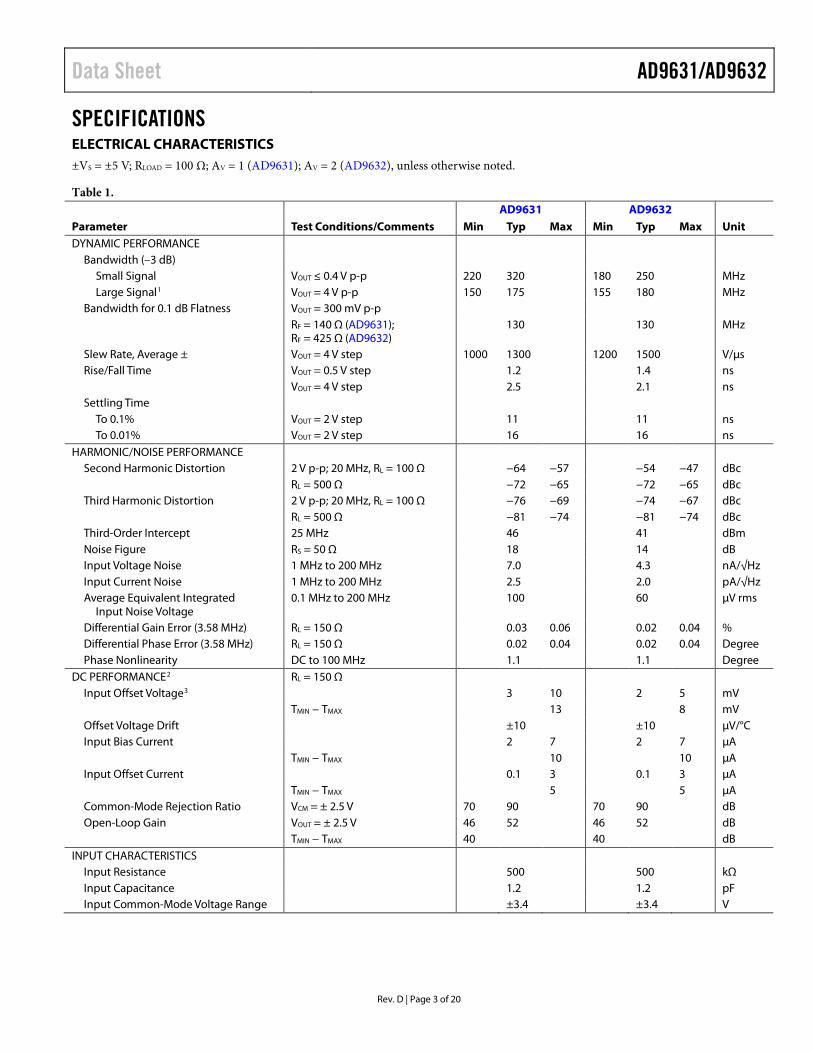
SPECIFICATIONS ELECTRICAL CHARACTERISTICS ±VS = ±5 V; RLOAD = 100 Ω; AV = 1 (AD9631); AV = 2 (AD9632), unless otherwise noted.
Table 1.
Parameter Test Conditions/Comments AD9631 AD9632
Unit Min Typ Max Min Typ Max DYNAMIC PERFORMANCE
Bandwidth (–3 dB) Small Signal VOUT ≤ 0.4 V p-p 220 320 180 250 MHz Large Signal1 VOUT = 4 V p-p 150 175 155 180 MHz
Bandwidth for 0.1 dB Flatness VOUT = 300 mV p-p RF = 140 Ω (AD9631);
RF = 425 Ω (AD9632) 130 130 MHz
Slew Rate, Average ± VOUT = 4 V step 1000 1300 1200 1500 V/μs Rise/Fall Time VOUT = 0.5 V step 1.2 1.4 ns VOUT = 4 V step 2.5 2.1 ns Settling Time
To 0.1% VOUT = 2 V step 11 11 ns To 0.01% VOUT = 2 V step 16 16 ns
HARMONIC/NOISE PERFORMANCE Second Harmonic Distortion 2 V p-p; 20 MHz, RL = 100 Ω −64 −57 −54 −47 dBc RL = 500 Ω −72 −65 −72 −65 dBc Third Harmonic Distortion 2 V p-p; 20 MHz, RL = 100 Ω −76 −69 −74 −67 dBc RL = 500 Ω −81 −74 −81 −74 dBc Third-Order Intercept 25 MHz 46 41 dBm Noise Figure RS = 50 Ω 18 14 dB Input Voltage Noise 1 MHz to 200 MHz 7.0 4.3 nA/√Hz Input Current Noise 1 MHz to 200 MHz 2.5 2.0 pA/√Hz Average Equivalent Integrated
Input Noise Voltage 0.1 MHz to 200 MHz 100 60 μV rms
Differential Gain Error (3.58 MHz) RL = 150 Ω 0.03 0.06 0.02 0.04 % Differential Phase Error (3.58 MHz) RL = 150 Ω 0.02 0.04 0.02 0.04 Degree Phase Nonlinearity DC to 100 MHz 1.1 1.1 Degree
DC PERFORMANCE2 RL = 150 Ω Input Offset Voltage3 3 10 2 5 mV TMIN − TMAX 13 8 mV Offset Voltage Drift ±10 ±10 µV/°C Input Bias Current 2 7 2 7 µA TMIN − TMAX 10 10 µA Input Offset Current 0.1 3 0.1 3 µA TMIN − TMAX 5 5 µA Common-Mode Rejection Ratio VCM = ± 2.5 V 70 90 70 90 dB Open-Loop Gain VOUT = ± 2.5 V 46 52 46 52 dB TMIN − TMAX 40 40 dB
INPUT CHARACTERISTICS Input Resistance 500 500 kΩ Input Capacitance 1.2 1.2 pF Input Common-Mode Voltage Range ±3.4 ±3.4 V
AD9631/AD9632 Data Sheet
Rev. D | Page 4 of 20
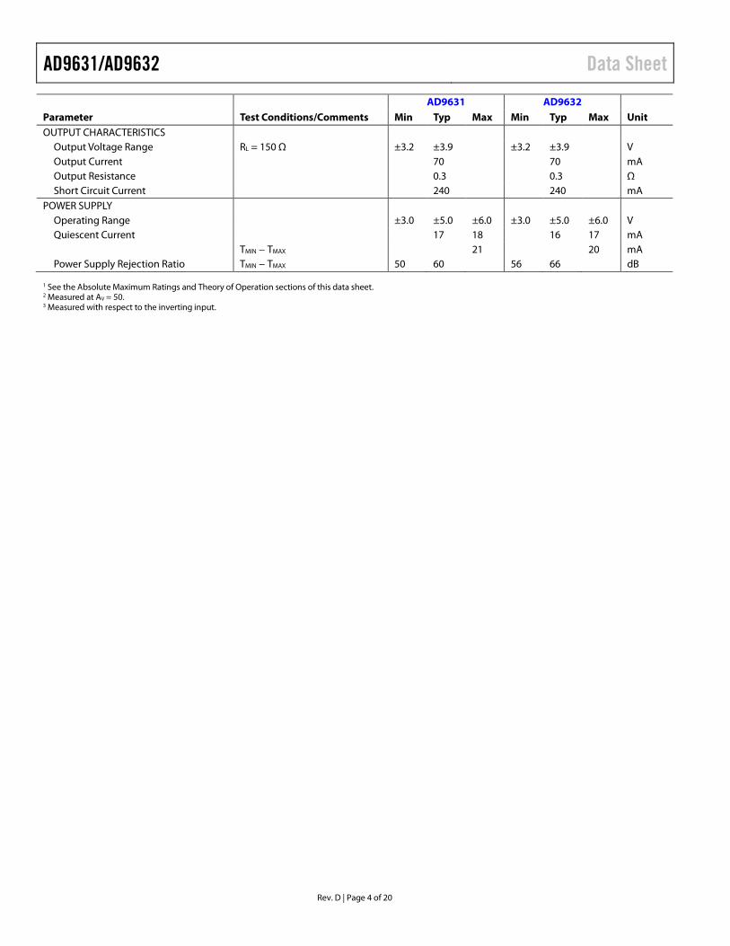
Parameter Test Conditions/Comments AD9631 AD9632
Unit Min Typ Max Min Typ Max OUTPUT CHARACTERISTICS
Output Voltage Range RL = 150 Ω ±3.2 ±3.9 ±3.2 ±3.9 V Output Current 70 70 mA Output Resistance 0.3 0.3 Ω Short Circuit Current 240 240 mA
POWER SUPPLY Operating Range ±3.0 ±5.0 ±6.0 ±3.0 ±5.0 ±6.0 V Quiescent Current 17 18 16 17 mA TMIN − TMAX 21 20 mA Power Supply Rejection Ratio TMIN − TMAX 50 60 56 66 dB
1 See the Absolute Maximum Ratings and Theory of Operation sections of this data sheet. 2 Measured at AV = 50. 3 Measured with respect to the inverting input.
Data Sheet AD9631/AD9632
Rev. D | Page 5 of 20
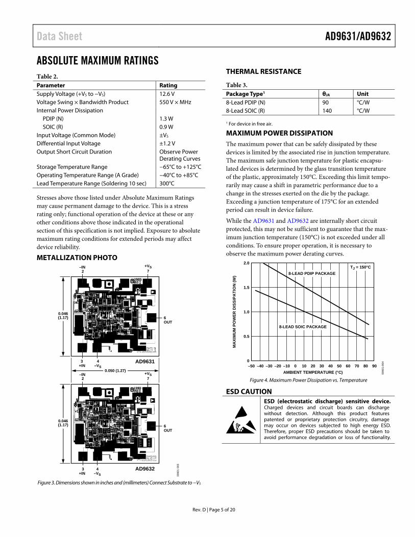
ABSOLUTE MAXIMUM RATINGS Table 2. Parameter Rating Supply Voltage (+VS to −VS) 12.6 V Voltage Swing × Bandwidth Product 550 V × MHz Internal Power Dissipation
PDIP (N) 1.3 W SOIC (R) 0.9 W
Input Voltage (Common Mode) ±VS Differential Input Voltage ±1.2 V Output Short Circuit Duration Observe Power
Derating Curves Storage Temperature Range −65°C to +125°C Operating Temperature Range (A Grade) −40°C to +85°C Lead Temperature Range (Soldering 10 sec) 300°C
Stresses above those listed under Absolute Maximum Ratings may cause permanent damage to the device. This is a stress rating only; functional operation of the device at these or any other conditions above those indicated in the operational section of this specification is not implied. Exposure to absolute maximum rating conditions for extended periods may affect device reliability.
METALLIZATION PHOTO
Figure 3. Dimensions shown in inches and (millimeters) Connect Substrate to −VS
THERMAL RESISTANCE
Table 3. Package Type1 θJA Unit 8-Lead PDIP (N) 90 °C/W 8-Lead SOIC (R) 140 °C/W
1 For device in free air.
MAXIMUM POWER DISSIPATION The maximum power that can be safely dissipated by these devices is limited by the associated rise in junction temperature. The maximum safe junction temperature for plastic encapsu-lated devices is determined by the glass transition temperature of the plastic, approximately 150°C. Exceeding this limit tempo-rarily may cause a shift in parametric performance due to a change in the stresses exerted on the die by the package. Exceeding a junction temperature of 175°C for an extended period can result in device failure.
While the AD9631 and AD9632 are internally short circuit protected, this may not be sufficient to guarantee that the max-imum junction temperature (150°C) is not exceeded under all conditions. To ensure proper operation, it is necessary to observe the maximum power derating curves.
Figure 4. Maximum Power Dissipation vs. Temperature
ESD CAUTION
AD9631
AD9632
–IN
–IN
2+VS
7
6OUT
2+VS
7
6OUT
3+IN
4–VS
3+IN
4–VS
0.046(1.17)
0.050 (1.27)
0.046(1.17)
0060
1-00
3
2.0
0
0.5
1.0
1.5
–50 –40 –30 –20 –10 0 10 20 30 40 50 60 70 80 90
MA
XIM
UM
PO
WER
DIS
SIPA
TIO
N (W
)
AMBIENT TEMPERATURE (°C)
8-LEAD SOIC PACKAGE
8-LEAD PDIP PACKAGETJ = 150°C
0060
1-00
4
AD9631/AD9632 Data Sheet
Rev. D | Page 6 of 20
TYPICAL PERFORMANCE CHARACTERISTICS
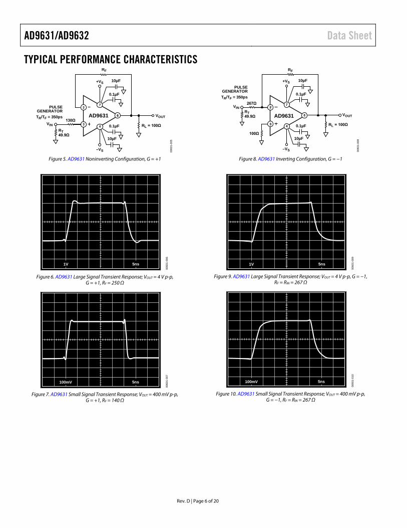
Figure 5. AD9631 Noninverting Configuration, G = +1
Figure 6. AD9631 Large Signal Transient Response; VOUT = 4 V p-p,
G = +1, RF = 250 Ω
Figure 7. AD9631 Small Signal Transient Response; VOUT = 400 mV p-p,
G = +1, RF = 140 Ω
Figure 8. AD9631 Inverting Configuration, G = −1
Figure 9. AD9631 Large Signal Transient Response; VOUT = 4 V p-p, G = −1,
RF = RIN = 267 Ω
Figure 10. AD9631 Small Signal Transient Response; VOUT = 400 mV p-p,
G = −1, RF = RIN = 267 Ω
AD9631
+VS
0.1µF
0.1µF
10µF
10µF
–VS
RF
130ΩVIN RL = 100Ω
VOUT
PULSEGENERATORTR/TF = 350ps
RT49.9Ω
0060
1-00
5
1V 5ns
0060
1-00
6
100mV 5ns
0060
1-00
7
AD9631
0.1µF
0.1µF
10µF
10µF+VS
–VS
RF
RL = 100Ω
VOUT
PULSEGENERATORTR/TF = 350ps
RT49.9Ω
267ΩVIN
100Ω
0060
1-00
8
1V 5ns
0060
1-00
9
100mV 5ns
0060
1-01
0
Data Sheet AD9631/AD9632
Rev. D | Page 7 of 20
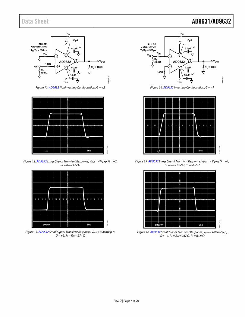
Figure 11. AD9632 Noninverting Configuration, G = +2
Figure 12. AD9632 Large Signal Transient Response; VOUT = 4 V p-p, G = +2, RF = RIN = 422 Ω
Figure 13. AD9632 Small Signal Transient Response; VOUT = 400 mV p-p,
G = +2, RF = RIN = 274 Ω
Figure 14. AD9632 Inverting Configuration, G = −1
Figure 15. AD9632 Large Signal Transient Response; VOUT = 4 V p-p, G = −1, RF = RIN = 422 Ω, RT = 56.2 Ω
Figure 16. AD9632 Small Signal Transient Response; VOUT = 400 mV p-p,
G = −1, RF = RIN = 267 Ω, RT = 61.9 Ω
PULSEGENERATORTR/TF = 350ps
RT49.9Ω
RIN
AD9632
+VS
0.1µF
0.1µF
10µF
10µF
–VS
RF
130ΩVIN RL = 100Ω
VOUT
0060
1-01
1
1V 5ns
0060
1-01
2
100mV 5ns
0060
1-01
3
PULSEGENERATORTR/TF = 350ps
RT49.9Ω
RIN
100Ω
VIN
AD9632
+VS
0.1µF
0.1µF
10µF
10µF
–VS
RF
RL = 100Ω
VOUT
0060
1-01
4
1V 5ns
0060
1-01
5
100mV 5ns
0060
1-01
6
AD9631/AD9632 Data Sheet
Rev. D | Page 8 of 20
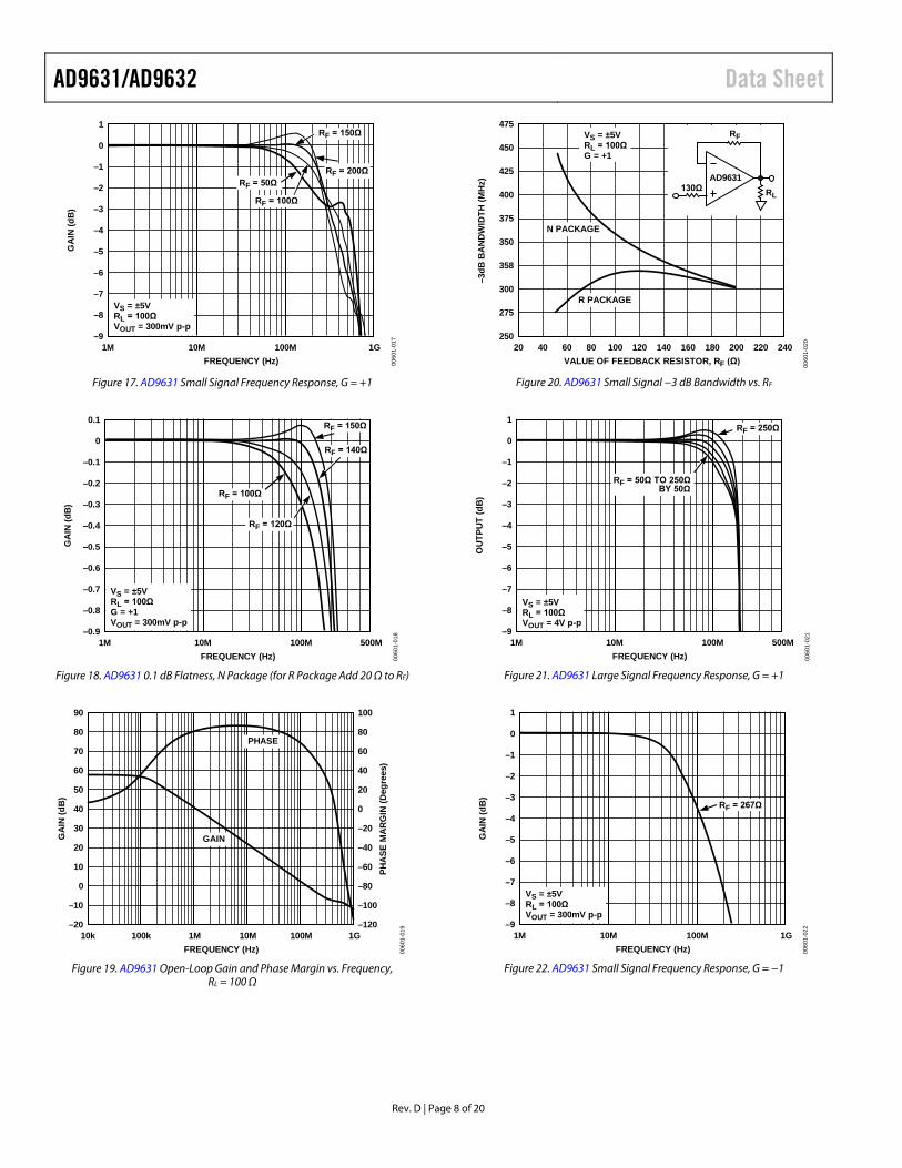
Figure 17. AD9631 Small Signal Frequency Response, G = +1
Figure 18. AD9631 0.1 dB Flatness, N Package (for R Package Add 20 Ω to RF)
Figure 19. AD9631 Open-Loop Gain and Phase Margin vs. Frequency,
RL = 100 Ω
Figure 20. AD9631 Small Signal −3 dB Bandwidth vs. RF
Figure 21. AD9631 Large Signal Frequency Response, G = +1
Figure 22. AD9631 Small Signal Frequency Response, G = −1
1
–9
–8
–7
–6
–5
–4
–3
–2
–1
0
1M 10M 100M 1G
GA
IN (d
B)
FREQUENCY (Hz)
VS = ±5VRL = 100ΩVOUT = 300mV p-p
RF = 200Ω
RF = 100Ω
RF = 50Ω
RF = 150Ω
0060
1-01
7
0.1
–0.9
–0.8
–0.7
–0.6
–0.5
–0.4
–0.3
–0.2
–0.1
0
1M 10M 100M 500M
GA
IN (d
B)
FREQUENCY (Hz)
VS = ±5VRL = 100ΩG = +1VOUT = 300mV p-p
RF = 150Ω
RF = 140Ω
RF = 100Ω
RF = 120Ω
0060
1-01
8
90
80
–20
–10
0
10
20
30
40
50
60
70
100
80
–120
–100
–80
–60
–40
–20
0
20
40
60
10k 100k 1M 10M 100M 1G
GA
IN (d
B)
PHA
SE M
AR
GIN
(Deg
rees
)
FREQUENCY (Hz)
PHASE
GAIN
0060
1-01
9
450
250
300
350
400
475
275
358
375
425
20 40 60 80 100 120 140 160 180 200 220 240
–3dB
BA
ND
WID
TH (M
Hz)
VALUE OF FEEDBACK RESISTOR, RF (Ω)
VS = ±5VRL = 100ΩG = +1
N PACKAGE
R PACKAGE
RF
RL130Ω
AD9631
0060
1-02
0
1
–9
–8
–7
–6
–5
–4
–3
–2
–1
0
1M 10M 100M 500M
OU
TPU
T (d
B)
FREQUENCY (Hz)
VS = ±5VRL = 100ΩVOUT = 4V p-p
RF = 250Ω
RF = 50Ω TO 250ΩBY 50Ω
0060
1-02
1
1
–9
–8
–7
–6
–5
–4
–3
–2
–1
0
1M 10M 100M 1G
GA
IN (d
B)
FREQUENCY (Hz)
VS = ±5VRL = 100ΩVOUT = 300mV p-p
RF = 267Ω00
601-
022
Data Sheet AD9631/AD9632
Rev. D | Page 9 of 20
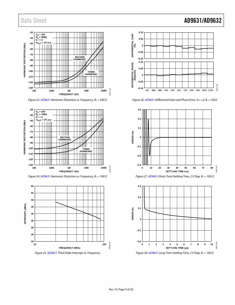
Figure 23. AD9631 Harmonic Distortion vs. Frequency, RL = 500 Ω
Figure 24. AD9631 Harmonic Distortion vs. Frequency, RL = 100 Ω
Figure 25. AD9631 Third Order Intercept vs. Frequency
Figure 26. AD9631 Differential Gain and Phase Error, G = +2, RL = 150 Ω
Figure 27. AD9631 Short-Term Settling Time, 2 V Step, RL = 100 Ω
Figure 28. AD9631 Long-Term Settling Time, 2 V Step, RL = 100 Ω
–30
–130
–120
–110
–100
–90
–80
–70
–60
–50
–40
10k 100k 1M 100M10M
HA
RM
ON
IC D
ISTO
RTI
ON
(dB
c)
FREQUENCY (Hz)
VS = ±5VRL = 500ΩG = +1VOUT = 2V p-p
SECONDHARMONIC
THIRDHARMONIC
0060
1-02
3–30
–130
–120
–110
–100
–90
–80
–70
–60
–50
–40
10k 100k 1M 100M10M
HA
RM
ON
IC D
ISTO
RTI
ON
(dB
c)
FREQUENCY (Hz)
VS = ±5VRL = 100ΩG = +1VOUT = 2V p-p
SECONDHARMONIC
THIRDHARMONIC
0060
1-02
4
60
20
25
30
35
40
45
50
55
10 100
INTE
RC
EPT
(dB
m)
FREQUENCY (MHz) 0060
1-02
5
–0.10
–0.05
0
0.05
0.10–0.10
–0.05
0
0.05
0.10
1ST 2ND 3RD 4TH 5TH 6TH 7TH 8TH 9TH 11TH10TH
DIF
FER
ENTI
AL
GA
IN(%
)D
IFFE
REN
TIA
L PH
ASE
(Deg
rees
)
0060
1-02
6
0.3
–0.3
–0.2
–0.1
0
0.1
0.2
0 10 20 30 40 50 60 70 80
ERR
OR
(%)
SETTLING TIME (ns) 0060
1-02
7
0.3
–0.2
–0.1
0
0.1
0.2
0 1 2 3 4 5 6 8 107 9
ERR
OR
(%)
SETTLING TIME (µs) 0060
1-02
8
AD9631/AD9632 Data Sheet
Rev. D | Page 10 of 20
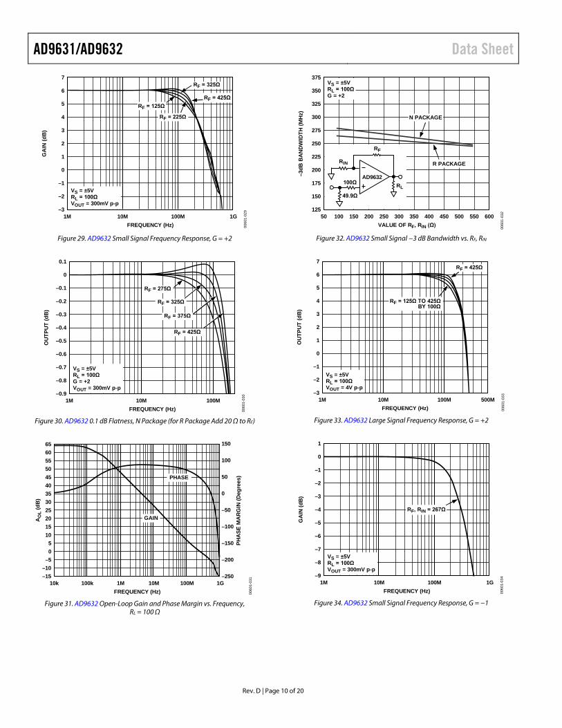
Figure 29. AD9632 Small Signal Frequency Response, G = +2
Figure 30. AD9632 0.1 dB Flatness, N Package (for R Package Add 20 Ω to RF)
Figure 31. AD9632 Open-Loop Gain and Phase Margin vs. Frequency,
RL = 100 Ω
Figure 32. AD9632 Small Signal −3 dB Bandwidth vs. RF, RIN
Figure 33. AD9632 Large Signal Frequency Response, G = +2
Figure 34. AD9632 Small Signal Frequency Response, G = −1
7
–3
–2
–1
0
1
2
3
4
5
6
1M 10M 100M 1G
GA
IN (d
B)
FREQUENCY (Hz)
VS = ±5VRL = 100ΩVOUT = 300mV p-p
RF = 425Ω
RF = 225Ω
RF = 125Ω
RF = 325Ω
0060
1-02
9
0.1
–0.9
–0.8
–0.7
–0.6
–0.5
–0.4
–0.3
–0.2
–0.1
0
1M 10M 100M
OU
TPU
T (d
B)
FREQUENCY (Hz)
VS = ±5VRL = 100ΩG = +2VOUT = 300mV p-p
RF = 275Ω
RF = 325Ω
RF = 375Ω
RF = 425Ω
0060
1-03
0
65
–15–10–505
1015202530354045505560
100
150
50
0
–50
–100
–150
–200
–25010k 100k 1M 10M 100M 1G
AO
L (d
B)
PHA
SE M
AR
GIN
(Deg
rees
)
FREQUENCY (Hz)
PHASE
GAIN
0060
1-03
1
375
350
325
300
275
250
225
200
175
150
12550 100 150 200 250 300 350 400 450 500 550 600
–3dB
BA
ND
WID
TH (M
Hz)
VALUE OF RF, RIN (Ω)
VS = ±5VRL = 100ΩG = +2
N PACKAGE
R PACKAGE
AD9632
RF
RL100Ω
49.9Ω
RIN
0060
1-03
2
7
–3
–2
–1
0
1
2
3
4
5
6
1M 10M 100M 500M
OU
TPU
T (d
B)
FREQUENCY (Hz)
VS = ±5VRL = 100ΩVOUT = 4V p-p
RF = 425Ω
RF = 125Ω TO 425ΩBY 100Ω
0060
1-03
3
1
–9
–8
–7
–6
–5
–4
–3
–2
–1
0
1M 10M 100M 1G
GA
IN (d
B)
FREQUENCY (Hz)
VS = ±5VRL = 100ΩVOUT = 300mV p-p
RF, RIN = 267Ω00
601-
034
Data Sheet AD9631/AD9632
Rev. D | Page 11 of 20
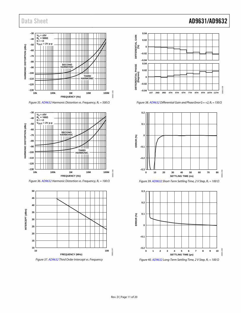
Figure 35. AD9632 Harmonic Distortion vs. Frequency, RL = 500 Ω
Figure 36. AD9632 Harmonic Distortion vs. Frequency, RL = 100 Ω
Figure 37. AD9632 Third Order Intercept vs. Frequency
Figure 38. AD9632 Differential Gain and Phase Error G = +2, RL = 150 Ω
Figure 39. AD9632 Short-Term Settling Time, 2 V Step, RL = 100 Ω
Figure 40. AD9632 Long-Term Settling Time, 2 V Step, RL = 100 Ω
–30
–130
–120
–110
–100
–90
–80
–70
–60
–50
–40
10k 100k 1M 100M10M
HA
RM
ON
IC D
ISTO
RTI
ON
(dB
c)
FREQUENCY (Hz)
VS = ±5VRL = 500ΩG = +2VOUT = 2V p-p
SECONDHARMONIC
THIRDHARMONIC
0060
1-03
5–30
–130
–120
–110
–100
–90
–80
–70
–60
–50
–40
10k 100k 1M 100M10M
HA
RM
ON
IC D
ISTO
RTI
ON
(dB
c)
FREQUENCY (Hz)
VS = ±5VRL = 100ΩG = +2VOUT = 2V p-p
SECONDHARMONIC
THIRDHARMONIC
0060
1-03
6
50
10
15
20
25
30
35
40
45
10 100
INTE
RC
EPT
(dB
m)
FREQUENCY (MHz) 0060
1-03
7
–0.04
–0.02
0
0.02
0.04–0.04
–0.02
0
0.02
0.04
1ST 2ND 3RD 4TH 5TH 6TH 7TH 8TH 9TH 11TH10TH
DIF
FER
ENTI
AL
GA
IN(%
)D
IFFE
REN
TIA
L PH
ASE
(Deg
rees
)
0060
1-03
8
0.2
–0.3
–0.2
–0.1
0
0.1
0 10 20 30 40 50 60 70 80
ERR
OR
(%)
SETTLING TIME (ns) 0060
1-03
9
0.3
–0.2
–0.1
0
0.1
0.2
0 1 2 3 4 5 6 8 107 9
ERR
OR
(%)
SETTLING TIME (µs) 0060
1-04
0
AD9631/AD9632 Data Sheet
Rev. D | Page 12 of 20
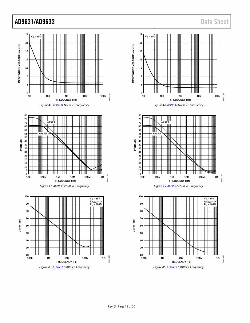
Figure 41. AD9631 Noise vs. Frequency
Figure 42. AD9631 PSRR vs. Frequency
Figure 43. AD9631 CMRR vs. Frequency
Figure 44. AD9632 Noise vs. Frequency
Figure 45. AD9632 PSRR vs. Frequency
Figure 46. AD9632 CMRR vs. Frequency
24
3
6
9
12
15
18
21
10 100 1k 100k10k
INPU
T N
OIS
E VO
LTA
GE
(nV√
Hz)
FREQUENCY (Hz)
VS = ±5V
0060
1-04
1
80757065
05
1015202530354045505560
10k 100k 1M 10M 100M 1G
PSR
R (d
B)
FREQUENCY (Hz)
–PSRR
+PSRR
0060
1-04
2
100
90
20
30
40
50
60
70
80
100k 1M 10M 1G100M
CM
RR
(dB
)
FREQUENCY (Hz)
VS = ±5VΔVCM = 1VRL = 100Ω
0060
1-04
3
17
3
5
7
9
11
13
15
10 100 1k 100k10k
INPU
T N
OIS
E VO
LTA
GE
(nV√
Hz)
FREQUENCY (Hz)
VS = ±5V
0060
1-04
4
80757065
05
1015202530354045505560
10k 100k 1M 10M 100M 1G
PSR
R (d
B)
FREQUENCY (Hz)
–PSRR
+PSRR
0060
1-04
5
100
90
20
30
40
50
60
70
80
100k 1M 10M 1G100M
CM
RR
(dB
)
FREQUENCY (Hz)
VS = ±5VΔVCM = 1VRL = 100Ω
0060
1-04
6
Data Sheet AD9631/AD9632
Rev. D | Page 13 of 20
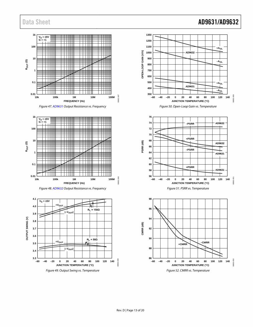
Figure 47. AD9631 Output Resistance vs. Frequency
Figure 48. AD9632 Output Resistance vs. Frequency
Figure 49. Output Swing vs. Temperature
Figure 50. Open-Loop Gain vs. Temperature
Figure 51. PSRR vs. Temperature
Figure 52. CMRR vs. Temperature
1k
0.01
0.1
1
10
100
10k 100k 1M 10M 100M
RO
UT
(Ω)
FREQUENCY (Hz)
VS = ±5VG = +1
0060
1-04
71k
0.01
0.1
1
10
100
10k 100k 1M 10M 100M
RO
UT
(Ω)
FREQUENCY (Hz)
VS = ±5VG = +1
0060
1-04
8
4.1
3.3
3.4
3.5
3.6
3.7
3.8
3.9
4.0
–60 –40 –20 0 20 40 60 80 100 120 140
OU
TPU
T SW
ING
(V)
JUNCTION TEMPERATURE (°C)
VS = ±5V+VOUT
RL = 150Ω
RL = 50Ω+VOUT
|–VOUT|
|–VOUT|
0060
1-04
9
1350
350
450
550
650
750
850
950
1050
1150
1250
–60 –40 –20 0 20 40 60 80 100 120 140
OPE
N-L
OO
P G
AIN
(V/V
)
JUNCTION TEMPERATURE (°C)
+AOL
AD9632
AD9631+AOL
–AOL
–AOL
0060
1-05
0
76
56
58
60
62
64
66
68
70
72
74
–60 –40 –20 0 20 40 60 80 100 120 140
PSR
R (d
B)
JUNCTION TEMPERATURE (°C)
AD9632
AD9632
AD9631
AD9631+PSRR
+PSRR
–PSRR
–PSRR
0060
1-05
1
98
96
94
92
90
88
86–60 –40 –20 0 20 40 60 80 100 120 140
CM
RR
(dB
)
JUNCTION TEMPERATURE (°C)
–CMRR+CMRR
0060
1-05
2
AD9631/AD9632 Data Sheet
Rev. D | Page 14 of 20
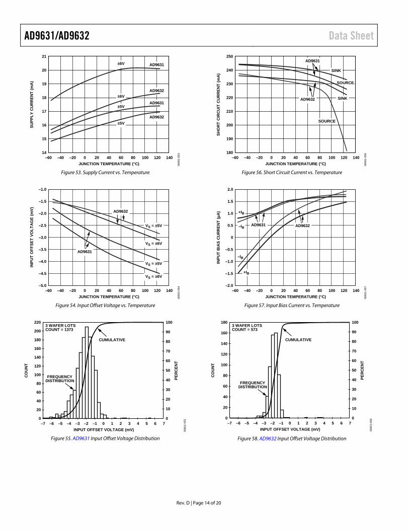
Figure 53. Supply Current vs. Temperature
Figure 54. Input Offset Voltage vs. Temperature
Figure 55. AD9631 Input Offset Voltage Distribution
Figure 56. Short Circuit Current vs. Temperature
Figure 57. Input Bias Current vs. Temperature
Figure 58. AD9632 Input Offset Voltage Distribution
21
20
19
18
17
16
15
14–60 –40 –20 0 20 40 60 80 100 120 140
SUPP
LY C
UR
REN
T (m
A)
JUNCTION TEMPERATURE (°C)
±6V
±6V
±5V
±5V
AD9631
AD9631
AD9632
AD9632
0060
1-05
3
–1.0
–5.0
–4.5
–4.0
–3.5
–3.0
–2.5
–2.0
–1.5
–60 –40 –20 0 20 40 60 80 100 120 140
INPU
T O
FFSE
T VO
LTA
GE
(mV)
JUNCTION TEMPERATURE (°C)
AD9631
AD9632
VS = ±5V
VS = ±5V
VS = ±6V
VS = ±6V
0060
1-05
4
220
0
20
40
60
80
100
120
140
160
180
200
100
0
10
20
30
40
50
60
70
80
90
–7 –6 –5 –4 –3 –2 –1 0 1 2 3 4 5 6 7
CO
UN
T
PER
CEN
T
INPUT OFFSET VOLTAGE (mV)
CUMULATIVE
FREQUENCYDISTRIBUTION
3 WAFER LOTSCOUNT = 1373
0060
1-05
5
250
180
190
200
210
220
230
240
–60 –40 –20 0 20 40 60 80 100 120 140
SHO
RT
CIR
CU
IT C
UR
REN
T (m
A)
JUNCTION TEMPERATURE (°C)
AD9631
AD9632
SINK
SINK
SOURCE
SOURCE
0060
1-05
6
2.0
–2.0
–1.5
–1.0
–0.5
0
0.5
1.0
1.5
–60 –40 –20 0 20 40 60 80 100 120 140
INPU
T B
IAS
CU
RR
ENT
(µA
)
JUNCTION TEMPERATURE (°C)
AD9631 AD9632
+IB
+IB
–IB
–IB
0060
1-05
7
180
0
20
40
60
80
100
120
140
160
100
0
10
20
30
40
50
60
70
80
90
–7 –6 –5 –4 –3 –2 –1 0 1 2 3 4 5 6 7
CO
UN
T
PER
CEN
T
INPUT OFFSET VOLTAGE (mV)
CUMULATIVE
FREQUENCYDISTRIBUTION
3 WAFER LOTSCOUNT = 573
0060
1-05
8
Data Sheet AD9631/AD9632
Rev. D | Page 15 of 20
THEORY OF OPERATION GENERAL The AD9631/AD9632 are wide bandwidth, voltage feedback amplifiers. Because their open-loop frequency response follows the conventional 6 dB/octave roll-off, their gain bandwidth product is basically constant. Increasing their closed-loop gain results in a corresponding decrease in small signal bandwidth. This can be observed by noting the bandwidth specification between the AD9631 (gain of +1) and AD9632 (gain of +2). The AD9631/AD9632 typically maintain 65° of phase margin. This high margin minimizes the effects of signal and noise peaking.
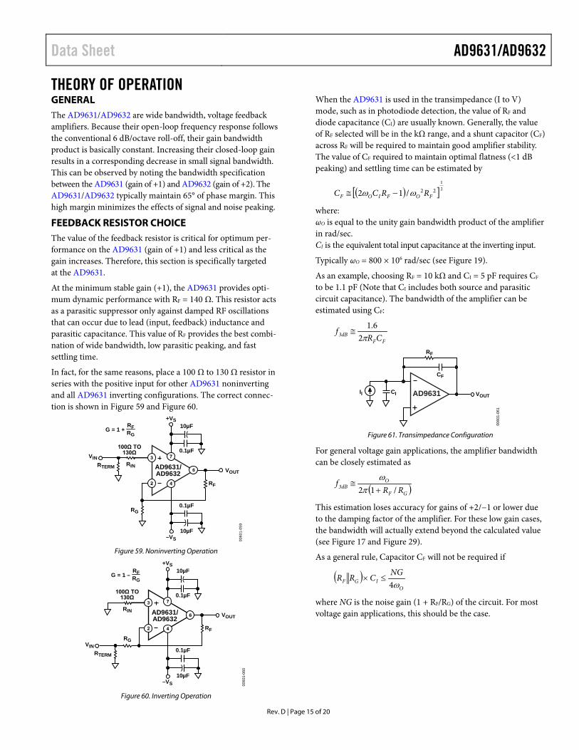
FEEDBACK RESISTOR CHOICE The value of the feedback resistor is critical for optimum per-formance on the AD9631 (gain of +1) and less critical as the gain increases. Therefore, this section is specifically targeted at the AD9631.
At the minimum stable gain (+1), the AD9631 provides opti-mum dynamic performance with RF = 140 Ω. This resistor acts as a parasitic suppressor only against damped RF oscillations that can occur due to lead (input, feedback) inductance and parasitic capacitance. This value of RF provides the best combi-nation of wide bandwidth, low parasitic peaking, and fast settling time.
In fact, for the same reasons, place a 100 Ω to 130 Ω resistor in series with the positive input for other AD9631 noninverting and all AD9631 inverting configurations. The correct connec-tion is shown in Figure 59 and Figure 60.
Figure 59. Noninverting Operation
Figure 60. Inverting Operation
When the AD9631 is used in the transimpedance (I to V) mode, such as in photodiode detection, the value of RF and diode capacitance (CI) are usually known. Generally, the value of RF selected will be in the kΩ range, and a shunt capacitor (CF) across RF will be required to maintain good amplifier stability. The value of CF required to maintain optimal flatness (<1 dB peaking) and settling time can be estimated by
( )[ ]21
22/12 FOFIOF RRCC ωω −≅
where: ωO is equal to the unity gain bandwidth product of the amplifier in rad/sec. CI is the equivalent total input capacitance at the inverting input.
Typically ωO = 800 × 106 rad/sec (see Figure 19).
As an example, choosing RF = 10 kΩ and CI = 5 pF requires CF to be 1.1 pF (Note that CI includes both source and parasitic circuit capacitance). The bandwidth of the amplifier can be estimated using CF:
FF3dB CRf
π26.1
≅
Figure 61. Transimpedance Configuration
For general voltage gain applications, the amplifier bandwidth can be closely estimated as
( )GF
O3dB RRf
/12 +≅
πω
This estimation loses accuracy for gains of +2/−1 or lower due to the damping factor of the amplifier. For these low gain cases, the bandwidth will actually extend beyond the calculated value (see Figure 17 and Figure 29).
As a general rule, Capacitor CF will not be required if
( )O
IGFNG
CRRω4
≤×
where NG is the noise gain (1 + RF/RG) of the circuit. For most voltage gain applications, this should be the case.
+VS
0.1µF
0.1µF
10µF
10µF
–VS
100Ω TO130Ω
RINRTERM
VIN
VOUT
RF
RG
RFRG
G = 1 +
AD9631/AD9632
0060
1-05
9
+VS
0.1µF
0.1µF
10µF
10µF
–VS
RTERM
VIN
VOUT
RF
RG
RFRG
G = 1 –
AD9631/AD9632
100Ω TO130Ω
RIN
0060
1-06
0
VOUT
RF
CF
CIII AD9631
0060
1-06
1

AD9631/AD9632 Data Sheet
Rev. D | Page 16 of 20
PULSE RESPONSE Unlike a traditional voltage feedback amplifier, where the slew speed is dictated by its front end dc quiescent current and gain bandwidth product, the AD9631/AD9632 provide on-demand current that increases proportionally to the input step signal amplitude. This results in slew rates (1300 V/µs) comparable to wideband current feedback designs. This, combined with relatively low input noise current (2.0 pA/√Hz), gives the AD9631/AD9632 the best attributes of both voltage and current feedback amplifiers.
LARGE SIGNAL PERFORMANCE The outstanding large signal operation of the AD9631 and AD9632 is due to a unique, proprietary design architecture. To maintain this level of performance, the maximum 550 V × MHz product must be observed (for example, @ 100 MHz, VOUT ≤ 5.5 V p-p).
POWER SUPPLY BYPASSING Adequate power supply bypassing can be critical when optimiz-ing the performance of a high frequency circuit. Inductance in the power supply leads can form resonant circuits that produce peaking in the amplifier’s response. In addition, if large current transients must be delivered to the load, then bypass capacitors (typically greater than 1 µF) will be required to provide the best settling time and lowest distortion. A parallel combination of at least 4.7 µF, and between 0.1 µF and 0.01 µF, is recommended. Some brands of electrolytic capacitors will require a small series damping resistor ≈4.7 Ω for optimum results.
DRIVING CAPACITIVE LOADS The AD9631/AD9632 were designed primarily to drive non-reactive loads. If driving loads with a capacitive component is desired, the best frequency response is obtained by the addition of a small series resistance as shown in Figure 62. Figure 63 shows the optimum value for RSERIES vs. capacitive load. It is worth noting that the frequency response of the circuit when driving large capacitive loads will be dominated by the passive roll-off of RSERIES and CL.
Figure 62. Driving Capacitive Loads
Figure 63. Recommended RSERIES vs. Capacitive Load
RF
RSERIES
RIN
RIN
CLRL
1kΩ
AD9631/AD9632
0060
1-06
2
40
30
20
100 10 205 15 25
RSE
RIE
S (Ω
)
CL (pF)
0060
1-06
3
Data Sheet AD9631/AD9632
Rev. D | Page 17 of 20
APPLICATIONS INFORMATION The AD9631/AD9632 are voltage feedback amplifiers well suited for applications such as photodetectors, active filters, and log amplifiers. The wide bandwidth (320 MHz), phase margin (65°), low current noise (2.0 pA/√Hz), and slew rate (1300 V/µs) of the devices give higher performance capabilities to these applications over previous voltage feedback designs.
With a settling time of 16 ns to 0.01% and 11 ns to 0.1%, the devices are an excellent choice for DAC I/V conversion. The same characteristics along with low harmonic distortion make them a good choice for ADC buffering/amplification. With superb linearity at relatively high signal frequencies, the AD9631/AD9632 are ideal drivers for ADCs up to 12 bits.
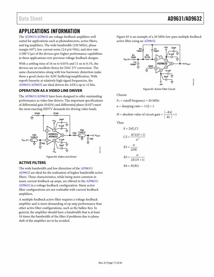
OPERATION AS A VIDEO LINE DRIVER The AD9631/AD9632 have been designed to offer outstanding performance as video line drivers. The important specifications of differential gain (0.02%) and differential phase (0.02°) meet the most exacting HDTV demands for driving video loads.
Figure 64. Video Line Driver
ACTIVE FILTERS The wide bandwidth and low distortion of the AD9631/ AD9632 are ideal for the realization of higher bandwidth active filters. These characteristics, while being more common in many current feedback op amps, are offered in the AD9631/ AD9632 in a voltage feedback configuration. Many active filter configurations are not realizable with current feedback amplifiers.
A multiple feedback active filter requires a voltage feedback amplifier and is more demanding of op amp performance than other active filter configurations, such as the Sallen-Key. In general, the amplifier should have a bandwidth that is at least 10 times the bandwidth of the filter if problems due to phase shift of the amplifier are to be avoided.
Figure 65 is an example of a 20 MHz low-pass multiple feedback active filter using an AD9632.
Figure 65. Active Filter Circuit
Choose
FO = cutoff frequency = 20 MHz
α = damping ratio = 1/Q = 2
H = absolute value of circuit gain = 114=
−RR
Then
12 CFk Oπ=
2)1(14
α+
=HC
C2
HKR1
2α
=
)1(2 +=
HKR3
α
)1(RHR4 =
+VS
0.1µF
0.1µF
10µF
10µF
–VS
VOUT
VIN
AD9631/AD9632
75Ω
75Ω
75Ω
274Ω 274Ω
75ΩCABLE
75ΩCABLE
0060
1-06
4
0.1µF
10µF
0.1µF
10µF
VOUT
VIN
+5V
–5V
AD9632100Ω
C150pF
R378.7Ω
R4154Ω
R1154Ω
C2100pF
0060
1-06
5
AD9631/AD9632 Data Sheet
Rev. D | Page 18 of 20
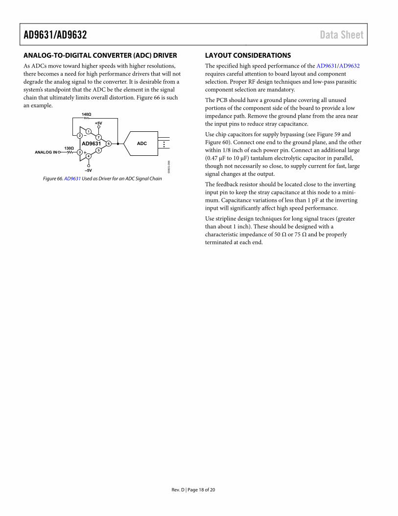
ANALOG-TO-DIGITAL CONVERTER (ADC) DRIVER As ADCs move toward higher speeds with higher resolutions, there becomes a need for high performance drivers that will not degrade the analog signal to the converter. It is desirable from a system’s standpoint that the ADC be the element in the signal chain that ultimately limits overall distortion. Figure 66 is such an example.
Figure 66. AD9631 Used as Driver for an ADC Signal Chain
LAYOUT CONSIDERATIONS The specified high speed performance of the AD9631/AD9632 requires careful attention to board layout and component selection. Proper RF design techniques and low-pass parasitic component selection are mandatory.
The PCB should have a ground plane covering all unused portions of the component side of the board to provide a low impedance path. Remove the ground plane from the area near the input pins to reduce stray capacitance.
Use chip capacitors for supply bypassing (see Figure 59 and Figure 60). Connect one end to the ground plane, and the other within 1/8 inch of each power pin. Connect an additional large (0.47 μF to 10 μF) tantalum electrolytic capacitor in parallel, though not necessarily so close, to supply current for fast, large signal changes at the output.
The feedback resistor should be located close to the inverting input pin to keep the stray capacitance at this node to a mini-mum. Capacitance variations of less than 1 pF at the inverting input will significantly affect high speed performance.
Use stripline design techniques for long signal traces (greater than about 1 inch). These should be designed with a characteristic impedance of 50 Ω or 75 Ω and be properly terminated at each end.
0060
1-06
6
+5V
–5V
130Ω
140Ω
ANALOG IN
AD9631 ADC
Data Sheet AD9631/AD9632
Rev. D | Page 19 of 20
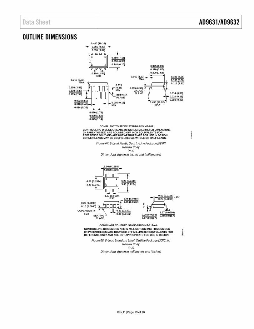
OUTLINE DIMENSIONS
Figure 67. 8-Lead Plastic Dual In-Line Package [PDIP]
Narrow Body (N-8)
Dimensions shown in inches and (millimeters)
Figure 68. 8-Lead Standard Small Outline Package [SOIC_N]
Narrow Body (R-8)
Dimensions shown in millimeters and (inches)
COMPLIANT TO JEDEC STANDARDS MS-001CONTROLLING DIMENSIONS ARE IN INCHES; MILLIMETER DIMENSIONS(IN PARENTHESES) ARE ROUNDED-OFF INCH EQUIVALENTS FORREFERENCE ONLY AND ARE NOT APPROPRIATE FOR USE IN DESIGN.CORNER LEADS MAY BE CONFIGURED AS WHOLE OR HALF LEADS. 07
0606
-A
0.022 (0.56)0.018 (0.46)0.014 (0.36)
SEATINGPLANE
0.015(0.38)MIN
0.210 (5.33)MAX
0.150 (3.81)0.130 (3.30)0.115 (2.92)
0.070 (1.78)0.060 (1.52)0.045 (1.14)
8
1 4
5 0.280 (7.11)0.250 (6.35)0.240 (6.10)
0.100 (2.54)BSC
0.400 (10.16)0.365 (9.27)0.355 (9.02)
0.060 (1.52)MAX
0.430 (10.92)MAX
0.014 (0.36)0.010 (0.25)0.008 (0.20)
0.325 (8.26)0.310 (7.87)0.300 (7.62)
0.195 (4.95)0.130 (3.30)0.115 (2.92)
0.015 (0.38)GAUGEPLANE
0.005 (0.13)MIN
CONTROLLING DIMENSIONS ARE IN MILLIMETERS; INCH DIMENSIONS(IN PARENTHESES) ARE ROUNDED-OFF MILLIMETER EQUIVALENTS FORREFERENCE ONLY AND ARE NOT APPROPRIATE FOR USE IN DESIGN.
COMPLIANT TO JEDEC STANDARDS MS-012-AA
0124
07-A
0.25 (0.0098)0.17 (0.0067)
1.27 (0.0500)0.40 (0.0157)
0.50 (0.0196)0.25 (0.0099) 45°
8°0°
1.75 (0.0688)1.35 (0.0532)
SEATINGPLANE
0.25 (0.0098)0.10 (0.0040)
41
8 5
5.00 (0.1968)4.80 (0.1890)
4.00 (0.1574)3.80 (0.1497)
1.27 (0.0500)BSC
6.20 (0.2441)5.80 (0.2284)
0.51 (0.0201)0.31 (0.0122)
COPLANARITY0.10
AD9631/AD9632 Data Sheet
Rev. D | Page 20 of 20
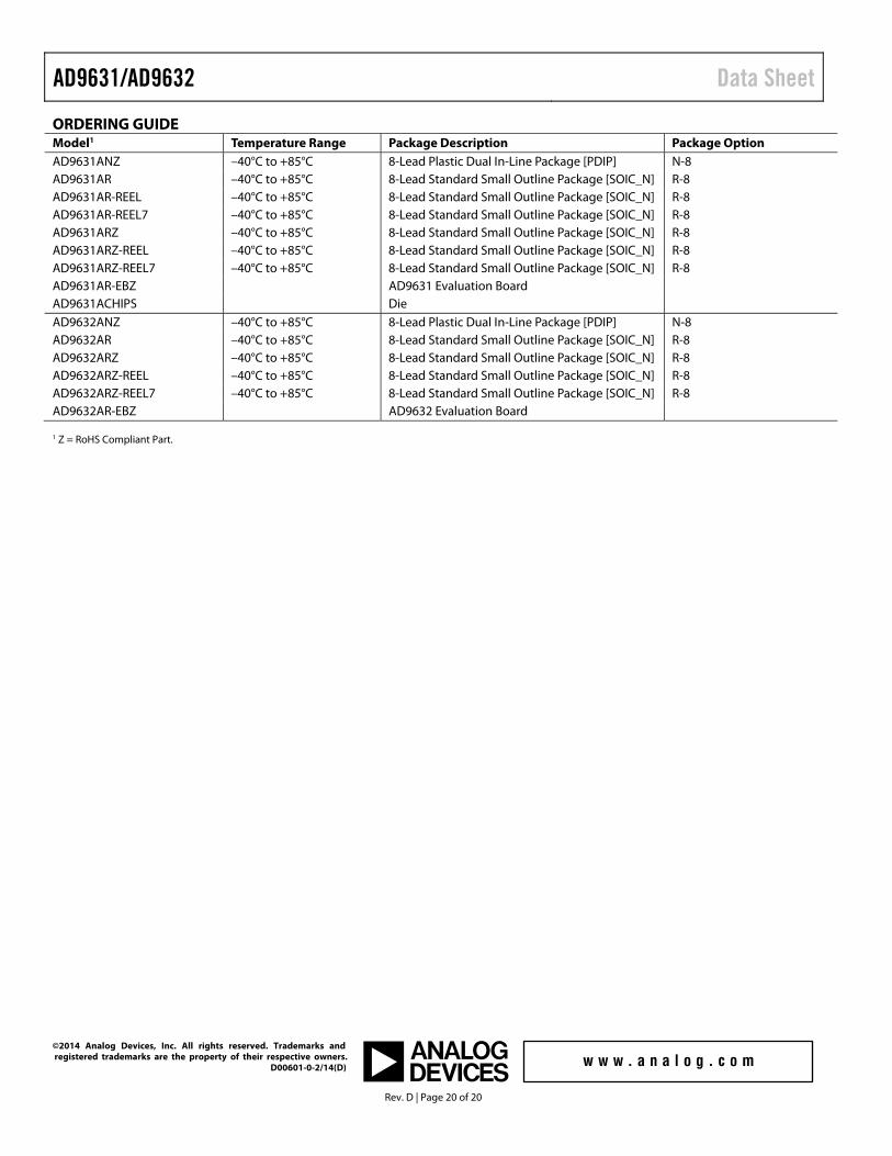
ORDERING GUIDE Model1 Temperature Range Package Description Package Option AD9631ANZ –40°C to +85°C 8-Lead Plastic Dual In-Line Package [PDIP] N-8 AD9631AR –40°C to +85°C 8-Lead Standard Small Outline Package [SOIC_N] R-8 AD9631AR-REEL –40°C to +85°C 8-Lead Standard Small Outline Package [SOIC_N] R-8 AD9631AR-REEL7 –40°C to +85°C 8-Lead Standard Small Outline Package [SOIC_N] R-8 AD9631ARZ –40°C to +85°C 8-Lead Standard Small Outline Package [SOIC_N] R-8 AD9631ARZ-REEL –40°C to +85°C 8-Lead Standard Small Outline Package [SOIC_N] R-8 AD9631ARZ-REEL7 –40°C to +85°C 8-Lead Standard Small Outline Package [SOIC_N] R-8 AD9631AR-EBZ AD9631 Evaluation Board AD9631ACHIPS Die AD9632ANZ –40°C to +85°C 8-Lead Plastic Dual In-Line Package [PDIP] N-8 AD9632AR –40°C to +85°C 8-Lead Standard Small Outline Package [SOIC_N] R-8 AD9632ARZ –40°C to +85°C 8-Lead Standard Small Outline Package [SOIC_N] R-8 AD9632ARZ-REEL –40°C to +85°C 8-Lead Standard Small Outline Package [SOIC_N] R-8 AD9632ARZ-REEL7 –40°C to +85°C 8-Lead Standard Small Outline Package [SOIC_N] R-8 AD9632AR-EBZ AD9632 Evaluation Board 1 Z = RoHS Compliant Part.
©2014 Analog Devices, Inc. All rights reserved. Trademarks and registered trademarks are the property of their respective owners. D00601-0-2/14(D)

![AD797 Ultralow Distortion, Ultralow Noise Op Amp Data ...Letoltesek/Audio Hifi Ic-k/AD797.pdf · 00846-001. Figure 1. 8-Lead Plastic Dual In-Line Package [PDIP] and 8-Lead Standard](https://img.pdfslide.net/doc/110x75/5f2c7372a5cc0d070922c652/ad797-ultralow-distortion-ultralow-noise-op-amp-data-letoltesekaudio-hifi.jpg)