Embed Size (px)
Citation preview
September 2009 Doc ID 15343 Rev 1 1/23
UM0674Application note
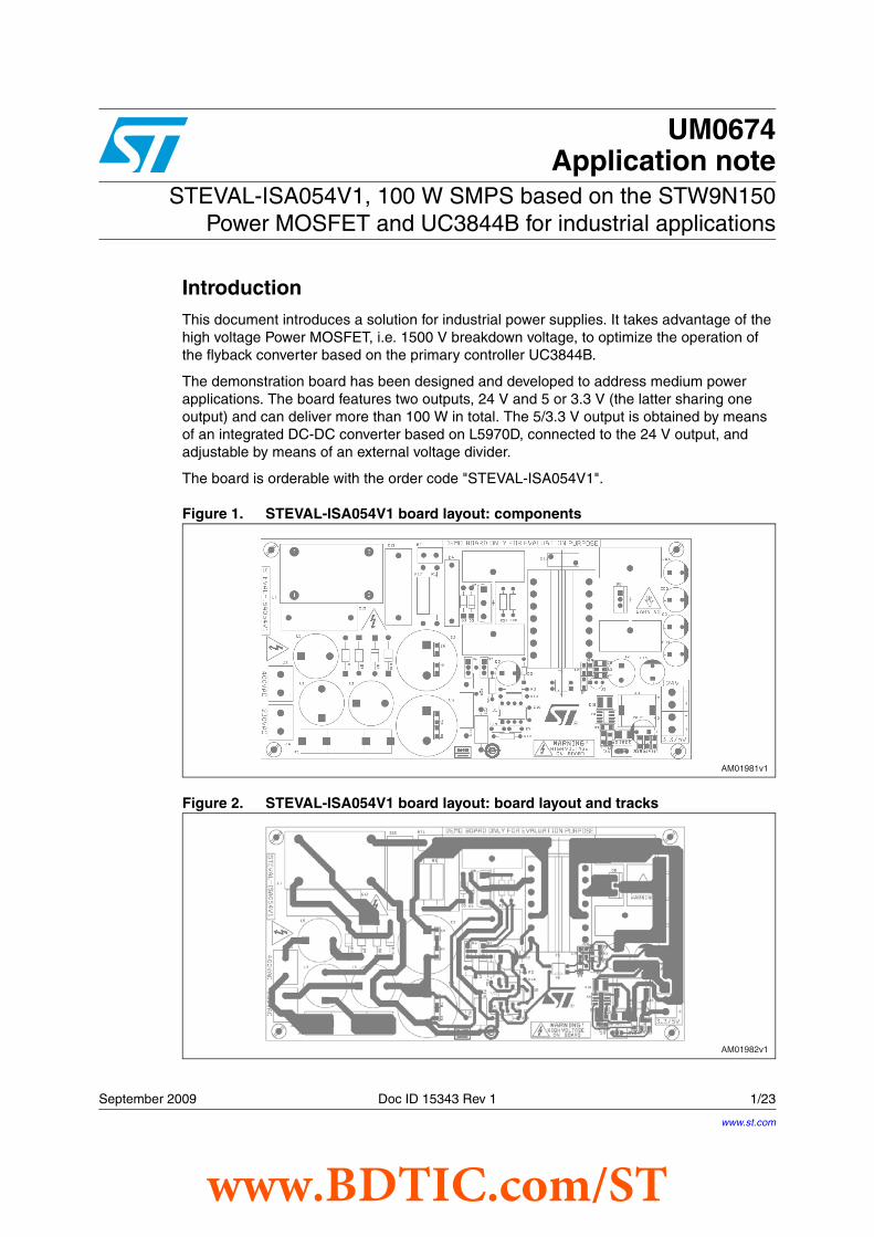
STEVAL-ISA054V1, 100 W SMPS based on the STW9N150Power MOSFET and UC3844B for industrial applications
IntroductionThis document introduces a solution for industrial power supplies. It takes advantage of the high voltage Power MOSFET, i.e. 1500 V breakdown voltage, to optimize the operation of the flyback converter based on the primary controller UC3844B.
The demonstration board has been designed and developed to address medium power applications. The board features two outputs, 24 V and 5 or 3.3 V (the latter sharing one output) and can deliver more than 100 W in total. The 5/3.3 V output is obtained by means of an integrated DC-DC converter based on L5970D, connected to the 24 V output, and adjustable by means of an external voltage divider.
The board is orderable with the order code "STEVAL-ISA054V1".
Figure 1. STEVAL-ISA054V1 board layout: components
Figure 2. STEVAL-ISA054V1 board layout: board layout and tracks
AM01981v1
AM01982v1
www.st.com
www.BDTIC.com/ST
Contents UM0674
2/23 Doc ID 15343 Rev 1
Contents
1 Demonstration board description . . . . . . . . . . . . . . . . . . . . . . . . . . . . . . 5
2 Specifics of the STW9N150 MOSFET . . . . . . . . . . . . . . . . . . . . . . . . . . . 9
3 Flyback transformer . . . . . . . . . . . . . . . . . . . . . . . . . . . . . . . . . . . . . . . . 11
3.1 Transformer specifications . . . . . . . . . . . . . . . . . . . . . . . . . . . . . . . . . . . . 12
4 DC-DC converter . . . . . . . . . . . . . . . . . . . . . . . . . . . . . . . . . . . . . . . . . . . 13
5 Primary and output waveforms . . . . . . . . . . . . . . . . . . . . . . . . . . . . . . . 14
5.1 Primary side waveforms . . . . . . . . . . . . . . . . . . . . . . . . . . . . . . . . . . . . . . 14
5.2 Output side waveforms . . . . . . . . . . . . . . . . . . . . . . . . . . . . . . . . . . . . . . . 15
6 System time response at load variations . . . . . . . . . . . . . . . . . . . . . . . 17
7 Efficiency . . . . . . . . . . . . . . . . . . . . . . . . . . . . . . . . . . . . . . . . . . . . . . . . . 18
8 Bill of material . . . . . . . . . . . . . . . . . . . . . . . . . . . . . . . . . . . . . . . . . . . . . 19
9 Conclusion . . . . . . . . . . . . . . . . . . . . . . . . . . . . . . . . . . . . . . . . . . . . . . . . 21
10 Revision history . . . . . . . . . . . . . . . . . . . . . . . . . . . . . . . . . . . . . . . . . . . 22
www.BDTIC.com/ST
UM0674 List of tables
Doc ID 15343 Rev 1 3/23
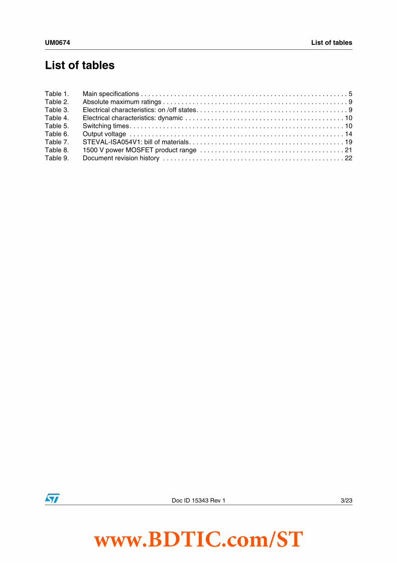
List of tables
Table 1. Main specifications . . . . . . . . . . . . . . . . . . . . . . . . . . . . . . . . . . . . . . . . . . . . . . . . . . . . . . . . 5Table 2. Absolute maximum ratings . . . . . . . . . . . . . . . . . . . . . . . . . . . . . . . . . . . . . . . . . . . . . . . . . . 9Table 3. Electrical characteristics: on /off states. . . . . . . . . . . . . . . . . . . . . . . . . . . . . . . . . . . . . . . . . 9Table 4. Electrical characteristics: dynamic . . . . . . . . . . . . . . . . . . . . . . . . . . . . . . . . . . . . . . . . . . . 10Table 5. Switching times. . . . . . . . . . . . . . . . . . . . . . . . . . . . . . . . . . . . . . . . . . . . . . . . . . . . . . . . . . 10Table 6. Output voltage . . . . . . . . . . . . . . . . . . . . . . . . . . . . . . . . . . . . . . . . . . . . . . . . . . . . . . . . . . 14Table 7. STEVAL-ISA054V1: bill of materials. . . . . . . . . . . . . . . . . . . . . . . . . . . . . . . . . . . . . . . . . . 19Table 8. 1500 V power MOSFET product range . . . . . . . . . . . . . . . . . . . . . . . . . . . . . . . . . . . . . . . 21Table 9. Document revision history . . . . . . . . . . . . . . . . . . . . . . . . . . . . . . . . . . . . . . . . . . . . . . . . . 22
www.BDTIC.com/ST
List of figures UM0674
4/23 Doc ID 15343 Rev 1
List of figures
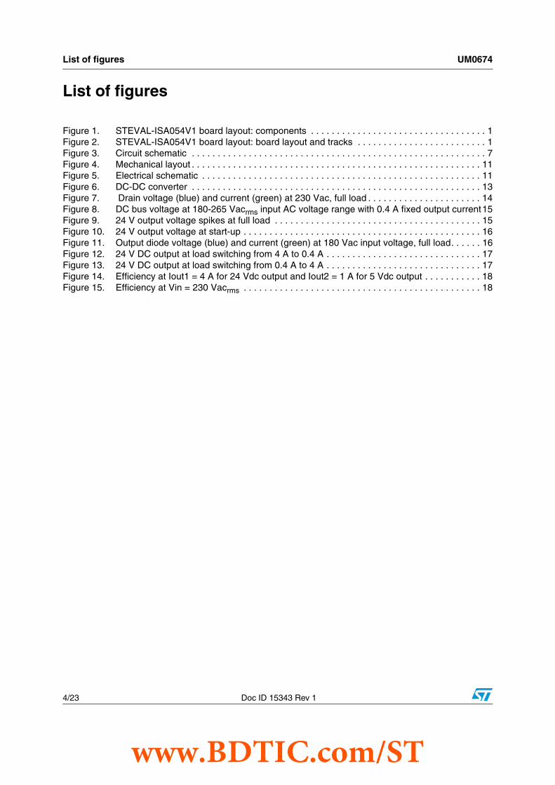
Figure 1. STEVAL-ISA054V1 board layout: components . . . . . . . . . . . . . . . . . . . . . . . . . . . . . . . . . . 1Figure 2. STEVAL-ISA054V1 board layout: board layout and tracks . . . . . . . . . . . . . . . . . . . . . . . . . 1Figure 3. Circuit schematic . . . . . . . . . . . . . . . . . . . . . . . . . . . . . . . . . . . . . . . . . . . . . . . . . . . . . . . . . 7Figure 4. Mechanical layout . . . . . . . . . . . . . . . . . . . . . . . . . . . . . . . . . . . . . . . . . . . . . . . . . . . . . . . . 11Figure 5. Electrical schematic . . . . . . . . . . . . . . . . . . . . . . . . . . . . . . . . . . . . . . . . . . . . . . . . . . . . . . 11Figure 6. DC-DC converter . . . . . . . . . . . . . . . . . . . . . . . . . . . . . . . . . . . . . . . . . . . . . . . . . . . . . . . . 13Figure 7. Drain voltage (blue) and current (green) at 230 Vac, full load . . . . . . . . . . . . . . . . . . . . . . 14Figure 8. DC bus voltage at 180-265 Vacrms input AC voltage range with 0.4 A fixed output current15Figure 9. 24 V output voltage spikes at full load . . . . . . . . . . . . . . . . . . . . . . . . . . . . . . . . . . . . . . . . 15Figure 10. 24 V output voltage at start-up . . . . . . . . . . . . . . . . . . . . . . . . . . . . . . . . . . . . . . . . . . . . . . 16Figure 11. Output diode voltage (blue) and current (green) at 180 Vac input voltage, full load. . . . . . 16Figure 12. 24 V DC output at load switching from 4 A to 0.4 A . . . . . . . . . . . . . . . . . . . . . . . . . . . . . . 17Figure 13. 24 V DC output at load switching from 0.4 A to 4 A . . . . . . . . . . . . . . . . . . . . . . . . . . . . . . 17Figure 14. Efficiency at Iout1 = 4 A for 24 Vdc output and Iout2 = 1 A for 5 Vdc output . . . . . . . . . . . 18Figure 15. Efficiency at Vin = 230 Vacrms . . . . . . . . . . . . . . . . . . . . . . . . . . . . . . . . . . . . . . . . . . . . . . 18
www.BDTIC.com/ST
UM0674 Demonstration board description
Doc ID 15343 Rev 1 5/23
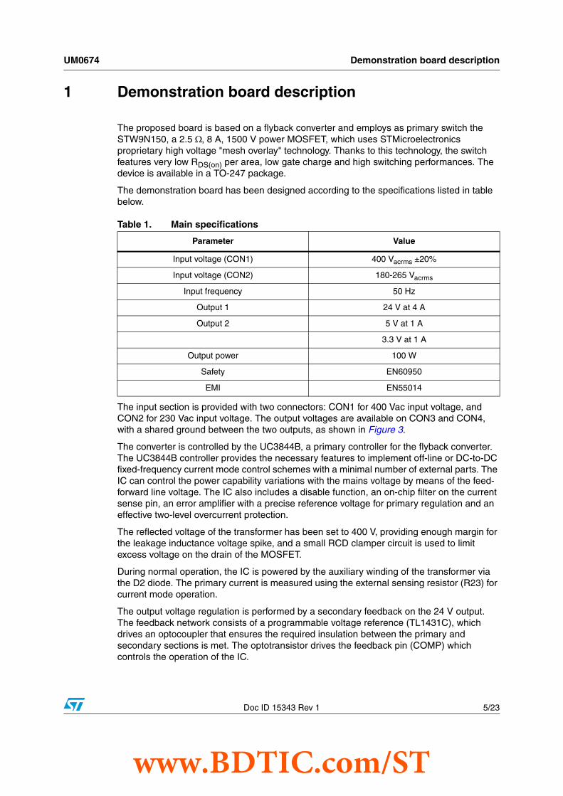
1 Demonstration board description
The proposed board is based on a flyback converter and employs as primary switch the STW9N150, a 2.5 Ω, 8 A, 1500 V power MOSFET, which uses STMicroelectronics proprietary high voltage "mesh overlay" technology. Thanks to this technology, the switch features very low RDS(on) per area, low gate charge and high switching performances. The device is available in a TO-247 package.
The demonstration board has been designed according to the specifications listed in table below.
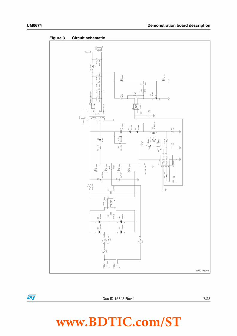
The input section is provided with two connectors: CON1 for 400 Vac input voltage, and CON2 for 230 Vac input voltage. The output voltages are available on CON3 and CON4, with a shared ground between the two outputs, as shown in Figure 3.
The converter is controlled by the UC3844B, a primary controller for the flyback converter. The UC3844B controller provides the necessary features to implement off-line or DC-to-DC fixed-frequency current mode control schemes with a minimal number of external parts. The IC can control the power capability variations with the mains voltage by means of the feed-forward line voltage. The IC also includes a disable function, an on-chip filter on the current sense pin, an error amplifier with a precise reference voltage for primary regulation and an effective two-level overcurrent protection.
The reflected voltage of the transformer has been set to 400 V, providing enough margin for the leakage inductance voltage spike, and a small RCD clamper circuit is used to limit excess voltage on the drain of the MOSFET.
During normal operation, the IC is powered by the auxiliary winding of the transformer via the D2 diode. The primary current is measured using the external sensing resistor (R23) for current mode operation.
The output voltage regulation is performed by a secondary feedback on the 24 V output. The feedback network consists of a programmable voltage reference (TL1431C), which drives an optocoupler that ensures the required insulation between the primary and secondary sections is met. The optotransistor drives the feedback pin (COMP) which controls the operation of the IC.
Table 1. Main specifications
Parameter Value
Input voltage (CON1) 400 Vacrms ±20%
Input voltage (CON2) 180-265 Vacrms
Input frequency 50 Hz
Output 1 24 V at 4 A
Output 2 5 V at 1 A
3.3 V at 1 A
Output power 100 W
Safety EN60950
EMI EN55014
www.BDTIC.com/ST

Demonstration board description UM0674
6/23 Doc ID 15343 Rev 1
The flyback transformer is manufactured by Magnetica, and guarantees that the safety insulation is in accordance with the EN60950 low-voltage directive. Transformer specifications are detailed in Chapter 3.
www.BDTIC.com/ST
UM0674 Demonstration board description
Doc ID 15343 Rev 1 7/23
Figure 3. Circuit schematic
AM01983v1
C9
1nF
C10
1nF
+C
o1
560u
F 35
V+C2 68
uF45
0VJ2
CO
N3
12
D3
STT
H10
8
C4
2.2n
160
0V
+C
o4
560u
F 35
V
C13
47nF
-X2
R6
2.2K
1%
C15
2.2n
F-Y
1
+C
333
0uF
25V
D2
1N41
48 R17
330K
2W
+C5 68
uF 4
50V
R1
330K
2W
C12
47nF
-X2
F1
FU
SE
L1
28m
H
1
23
4
R29
12
R23
0.68
R19
1K
L6
10uH
t
NTC
- 1
0
L5 1mH
12
L2 1mH
12
L3 1mH
12
Q6
2SD
882
3
2 1
R26
1k
Q7
2SB
772
3
1 2
24V
+C
16
560u
F 3
5V
Q5
STW
9N15
01
2 3
R18
15K
D6
1N40
07
12
R27
27C
1410
nF
R28
12
R2
1M 1
/8W
I >
4A
J3CO
N1 12
J4CO
N2 12
+C
o2
560u
F 3
5V
R4
1M 1
/8W
R10
4.7K
C6
100n
F
R11
56K
U4 P
C81
7
R7
1M 1
/8W
D8
ST
PS
2012
0CFP
R9
1M 1
/8W
D5
STT
H10
8
R8
1K
D9
1N40
07
12
R13
47K
3W
R3
10
D10
1N40
07
12
+C
o3
560u
F 35
V
D11
1N40
07
12
T5
TRA
NSF
OR
ME
R
5 762
1012
R5
19K
1%
U3
TL14
31
21
3
U1
UC
3844
B
VFB
2
CO
MP
1
VR
EF
8
RT/
CT
4S
EN
SE
3O
UT
6
VCC7
GND5
www.BDTIC.com/ST
Demonstration board description UM0674
8/23 Doc ID 15343 Rev 1
The 5 V output is obtained from the 24 V output by means of an integrated power IC, the L5970D. The L5970D is a step-down monolithic power switching regulator with a switch current limit of 1 A, able to deliver up to 1 A DC current to the load depending on the application conditions. The output voltage can be adjusted by a voltage divider supplying either 3.3 V or 5 V. More detailed information on DC-DC conversion is introduced in Chapter 4.
The whole power supply has been realized on a single-side 35 µm PCB, whose total surface amounts to 176 x 90 mm.
www.BDTIC.com/ST
UM0674 Specifics of the STW9N150 MOSFET
Doc ID 15343 Rev 1 9/23
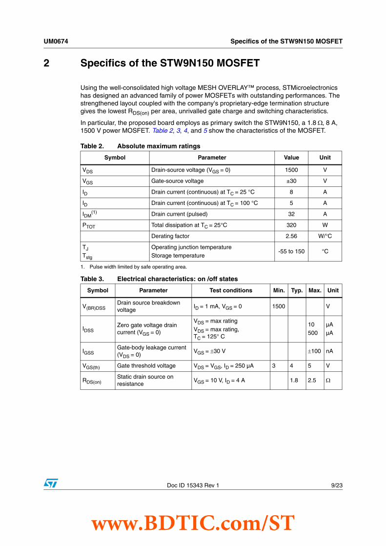
2 Specifics of the STW9N150 MOSFET
Using the well-consolidated high voltage MESH OVERLAY™ process, STMicroelectronics has designed an advanced family of power MOSFETs with outstanding performances. The strengthened layout coupled with the company's proprietary-edge termination structure gives the lowest RDS(on) per area, unrivalled gate charge and switching characteristics.
In particular, the proposed board employs as primary switch the STW9N150, a 1.8 Ω, 8 A, 1500 V power MOSFET. Table 2, 3, 4, and 5 show the characteristics of the MOSFET.
Table 2. Absolute maximum ratings
Symbol Parameter Value Unit
VDS Drain-source voltage (VGS = 0) 1500 V
VGS Gate-source voltage ±30 V
ID Drain current (continuous) at TC = 25 °C 8 A
ID Drain current (continuous) at TC = 100 °C 5 A
IDM(1)
1. Pulse width limited by safe operating area.
Drain current (pulsed) 32 A
PTOT Total dissipation at TC = 25°C 320 W
Derating factor 2.56 W/°C
TJ
Tstg
Operating junction temperatureStorage temperature
-55 to 150 °C
Table 3. Electrical characteristics: on /off states
Symbol Parameter Test conditions Min. Typ. Max. Unit
V(BR)DSSDrain source breakdown voltage
ID = 1 mA, VGS = 0 1500 V
IDSSZero gate voltage drain current (VGS = 0)
VDS = max rating
VDS = max rating, TC = 125° C
10500
µAµA
IGSSGate-body leakage current (VDS = 0)
VGS = ±30 V ±100 nA
VGS(th) Gate threshold voltage VDS = VGS, ID = 250 µA 3 4 5 V
RDS(on)Static drain source on resistance
VGS = 10 V, ID = 4 A 1.8 2.5 Ω
www.BDTIC.com/ST
Specifics of the STW9N150 MOSFET UM0674
10/23 Doc ID 15343 Rev 1
Table 4. Electrical characteristics: dynamic
Symbol Parameter Test conditions Min. Typ. Max. Unit
gfs(1)
1. Pulsed: Pulse duration = 300 µs, duty cycle 1.5%
Forward transconductance VDS = 15 V, ID = 4 A 7.5 S
CissCoss
Crss
Input capacitance
Output capacitanceReverse transfer capacitance
VDS = 25 V, f = 1 MHz, VGS = 0
3255
29422.4
pF
pFpF
Coss eq.Equivalent output capacitance
VGS = 0, VDS = 0 to 1200 V 118 pF
Rg Gate input resistancef = 1 MHz gate DC Blas = 0Test signal level = 20 mV open drain
2.4 Ω
Qg
Qgs
Qgd
Total gate charge
Gate-source chargeGate-drain charge
VDD = 1200 V, ID = 8 A, VGS = 10 V
89.3
15.850.4
nC
nCnC
Table 5. Switching times
Symbol Parameter Test conditions Min. Typ. Max. Unit
td(on)
trtd(off)
tf
Turn-on delay timeRise time
Turn-off delay time
Fall time
VDD = 750 V, ID = 4 A
RG = 4.7 Ω, VGS = 10 V
4114.7
86
52
nsns
ns
ns
www.BDTIC.com/ST
UM0674 Flyback transformer
Doc ID 15343 Rev 1 11/23
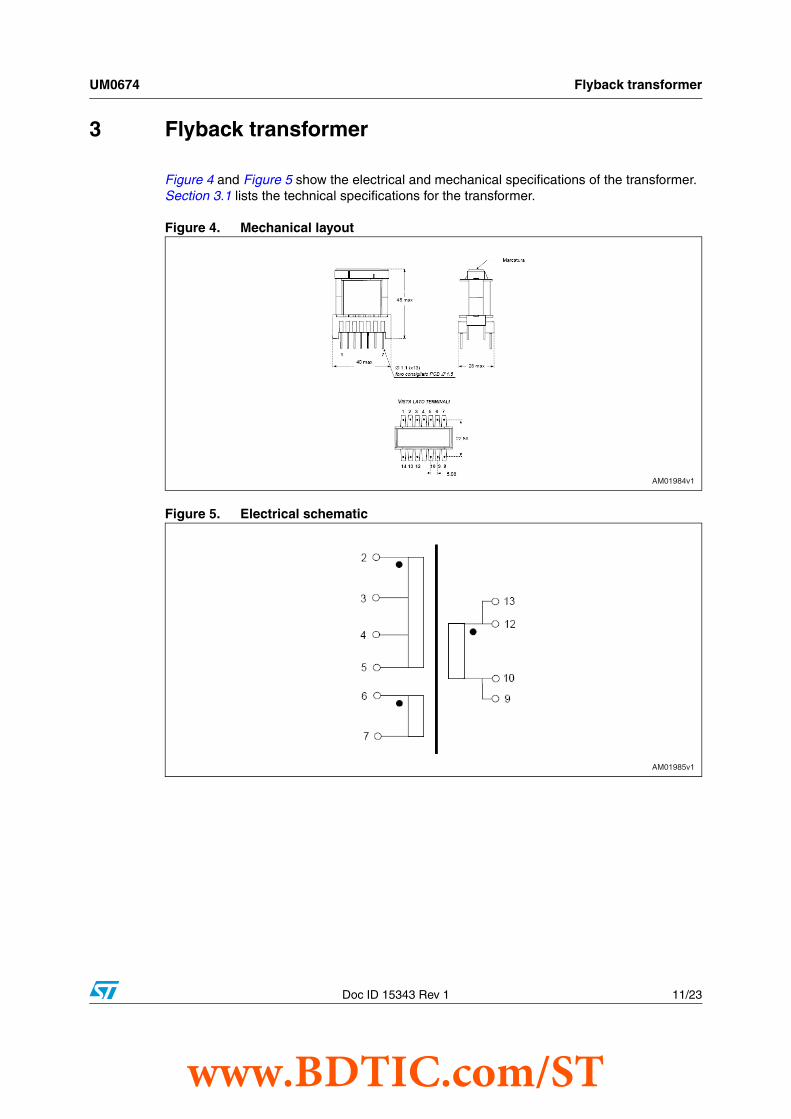
3 Flyback transformer
Figure 4 and Figure 5 show the electrical and mechanical specifications of the transformer. Section 3.1 lists the technical specifications for the transformer.
Figure 4. Mechanical layout
Figure 5. Electrical schematic
AM01984v1
AM01985v1
www.BDTIC.com/ST
Flyback transformer UM0674
12/23 Doc ID 15343 Rev 1
3.1 Transformer specifications● Inductance: (at 1 kHz, 20 deg C)
– Primary (pin 2-5): 2.25 mH +/-15 %
– Auxiliary (pin 6-7): 3.3 µH +/-15 %
– Secondary (pin 13,12-9,10): 9 µH +/-15 %
● Resistance: (at 20 deg C)
– Primary (pin 2-5): 0.8 mΩ max
– Auxiliary (pin 6-7): 45 mΩ max
– Secondary (pin 12-9): 13 mΩ max
– Secondary (pin 13-10): 15 mΩ max
● Transformer ratio: (at 10 kHz, 20 deg C)
– Terminals 2-5 / 6-7: 28 +/-5 %
– Terminals 2-5 / 13-9: 16 +/-5 %
– Terminals 2-5 / 12-10: 16 +/-5 %
● Inductance losses: (pin 2-5, 6-7-9-10-12-13 at 10 kHz, Ta 20 deg. C): 1 % NOM
● Parasitic capacitance: (pin 2-5 at 650 kHz, Ta 20 deg. C): 26 pF NOM
● Saturation current: (pin 2-5 at 0.35T Bsat, Ta 20 deg. C): 1.5 Ap max
● Working current: (pin 2-5 at Pmax 103 W, F 70 kHz, Ta 20 deg. C): 1.2 Ap max
● Working frequency: (at Pmax 103 W, 70 kHz, Ta 20 deg. C): 70 kHz nom
● Temperature: (at Pmax 103 W): -10/+40 deg C
● Primary/Secondary isolation: (at 50 Hz, time 2",Ta 20 deg. C): 4000 V
● Dimensions max: 40 x 28 mm, h 45 mm
● Weight: ∼ 68 g.
www.BDTIC.com/ST
UM0674 DC-DC converter
Doc ID 15343 Rev 1 13/23
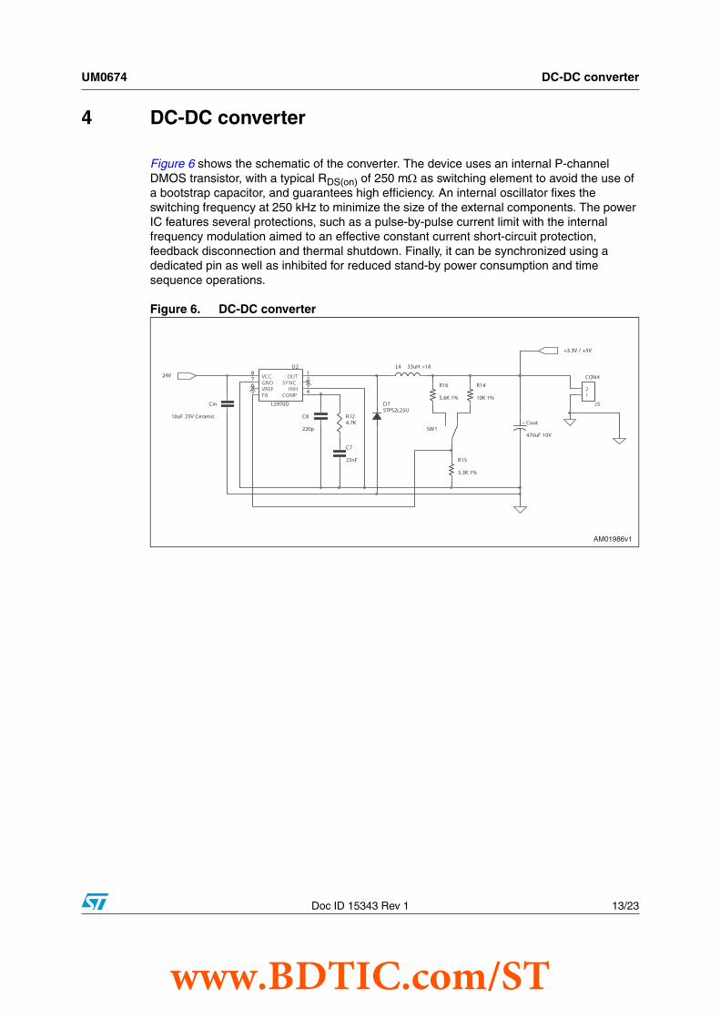
4 DC-DC converter
Figure 6 shows the schematic of the converter. The device uses an internal P-channel DMOS transistor, with a typical RDS(on) of 250 mΩ as switching element to avoid the use of a bootstrap capacitor, and guarantees high efficiency. An internal oscillator fixes the switching frequency at 250 kHz to minimize the size of the external components. The power IC features several protections, such as a pulse-by-pulse current limit with the internal frequency modulation aimed to an effective constant current short-circuit protection, feedback disconnection and thermal shutdown. Finally, it can be synchronized using a dedicated pin as well as inhibited for reduced stand-by power consumption and time sequence operations.
Figure 6. DC-DC converter
AM01986v1
R16
5.6K 1%
R14
10K 1%
SW1
U2
L5970D
OUT1
SYNC2
INH3
COMP4
FB5 VREF6 GND7 VCC8
Cin
10uF 25V Ceramic
C7
22nF
R124.7K
C8
220p
D7STPS2L25U
L4 33uH >1A
+ Cout
470uF 10V
24V
+3.3V / +5V
R15
3.3K 1%
J5
CON4
12
www.BDTIC.com/ST
Primary and output waveforms UM0674
14/23 Doc ID 15343 Rev 1
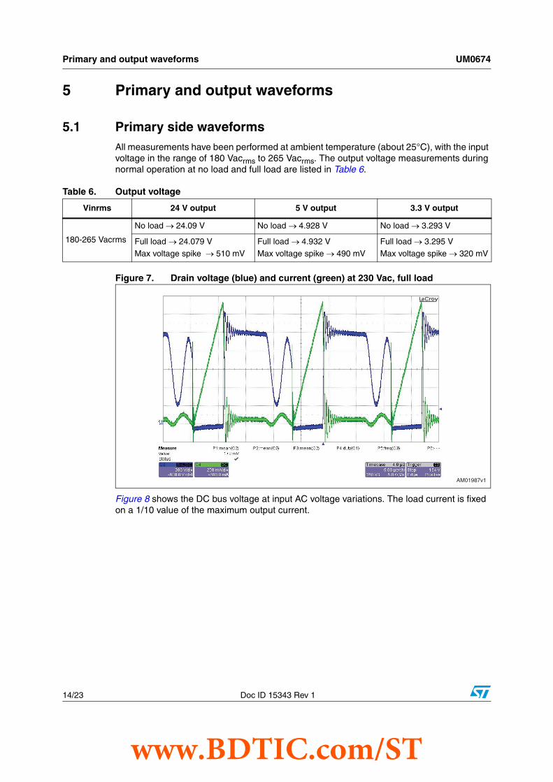
5 Primary and output waveforms
5.1 Primary side waveformsAll measurements have been performed at ambient temperature (about 25°C), with the input voltage in the range of 180 Vacrms to 265 Vacrms. The output voltage measurements during normal operation at no load and full load are listed in Table 6.
Figure 7. Drain voltage (blue) and current (green) at 230 Vac, full load
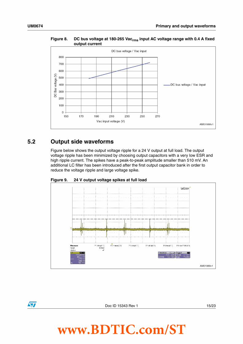
Figure 8 shows the DC bus voltage at input AC voltage variations. The load current is fixed on a 1/10 value of the maximum output current.
Table 6. Output voltage
Vinrms 24 V output 5 V output 3.3 V output
180-265 Vacrms
No load → 24.09 V No load → 4.928 V No load → 3.293 V
Full load → 24.079 VMax voltage spike → 510 mV
Full load → 4.932 VMax voltage spike → 490 mV
Full load → 3.295 VMax voltage spike → 320 mV
AM01987v1
www.BDTIC.com/ST
UM0674 Primary and output waveforms
Doc ID 15343 Rev 1 15/23
Figure 8. DC bus voltage at 180-265 Vacrms input AC voltage range with 0.4 A fixed output current
5.2 Output side waveformsFigure below shows the output voltage ripple for a 24 V output at full load. The output voltage ripple has been minimized by choosing output capacitors with a very low ESR and high ripple current. The spikes have a peak-to-peak amplitude smaller than 510 mV. An additional LC filter has been introduced after the first output capacitor bank in order to reduce the voltage ripple and large voltage spike.
Figure 9. 24 V output voltage spikes at full load
AM01989v1
www.BDTIC.com/ST
Primary and output waveforms UM0674
16/23 Doc ID 15343 Rev 1
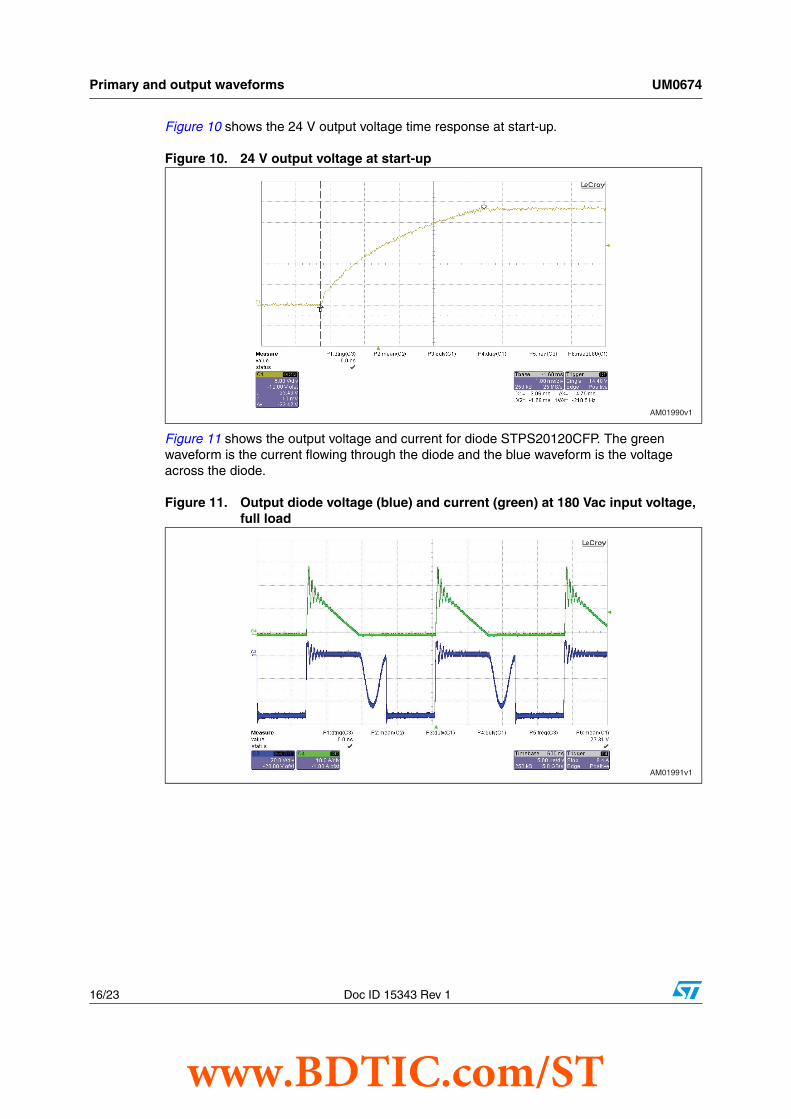
Figure 10 shows the 24 V output voltage time response at start-up.
Figure 10. 24 V output voltage at start-up
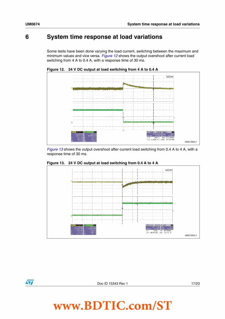
Figure 11 shows the output voltage and current for diode STPS20120CFP. The green waveform is the current flowing through the diode and the blue waveform is the voltage across the diode.
Figure 11. Output diode voltage (blue) and current (green) at 180 Vac input voltage, full load
AM01990v1
AM01991v1
www.BDTIC.com/ST
UM0674 System time response at load variations
Doc ID 15343 Rev 1 17/23
6 System time response at load variations
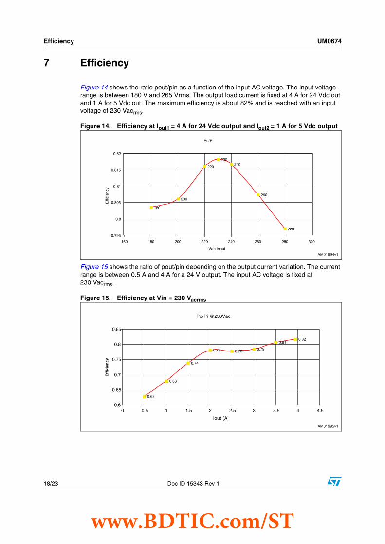
Some tests have been done varying the load current, switching between the maximum and minimum values and vice versa. Figure 12 shows the output overshoot after current load switching from 4 A to 0.4 A, with a response time of 30 ms.
Figure 12. 24 V DC output at load switching from 4 A to 0.4 A
Figure 13 shows the output overshoot after current load switching from 0.4 A to 4 A, with a response time of 30 ms.
Figure 13. 24 V DC output at load switching from 0.4 A to 4 A
AM01992v1
AM01993v1
www.BDTIC.com/ST
Efficiency UM0674
18/23 Doc ID 15343 Rev 1
7 Efficiency
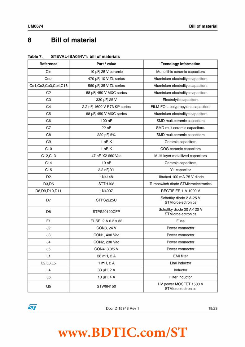
Figure 14 shows the ratio pout/pin as a function of the input AC voltage. The input voltage range is between 180 V and 265 Vrms. The output load current is fixed at 4 A for 24 Vdc out and 1 A for 5 Vdc out. The maximum efficiency is about 82% and is reached with an input voltage of 230 Vacrms.
Figure 14. Efficiency at Iout1 = 4 A for 24 Vdc output and Iout2 = 1 A for 5 Vdc output
Figure 15 shows the ratio of pout/pin depending on the output current variation. The current range is between 0.5 A and 4 A for a 24 V output. The input AC voltage is fixed at 230 Vacrms.
Figure 15. Efficiency at Vin = 230 Vacrms
AM01994v1
Po/Pi
180
200
220
230240
260
280
0.795
0.8
0.805
0.81
0.815
0.82
160 180 200 220 240 260 280 300
Vac input
Effi
cien
cy
AM01995v1
Po/Pi @230Vac
0.63
0.68
0.74
0.78 0.79
0.810.82
0.78
0.6
0.65
0.7
0.75
0.8
0.85
0 0.5 1 1.5 2 2.5 3 3.5 4 4.5
Iout (A)
Efficiency
www.BDTIC.com/ST
UM0674 Bill of material
Doc ID 15343 Rev 1 19/23
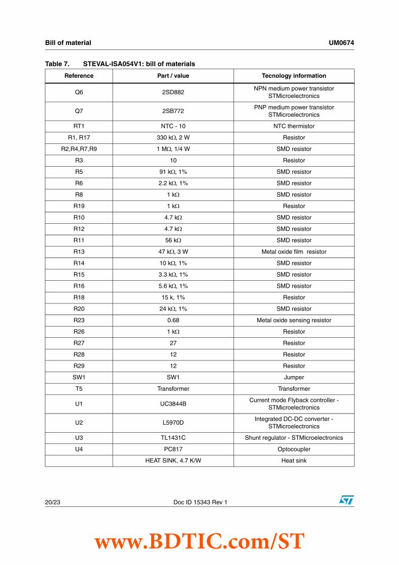
8 Bill of material
Table 7. STEVAL-ISA054V1: bill of materials
Reference Part / value Tecnology information
Cin 10 µF, 25 V ceramic Monolithic ceramic capacitors
Cout 470 µF, 10 V-ZL series Aluminium electrolityc capacitors
Co1,Co2,Co3,Co4,C16 560 µF, 35 V-ZL series Aluminium electrolityc capacitors
C2 68 µF, 450 V-MXC series Aluminium electrolityc capacitors
C3 330 µF, 25 V Electrolytic capacitors
C4 2.2 nF, 1600 V R73 KP series FILM-FOIL polypropylene capacitors
C5 68 µF, 450 V-MXC series Aluminium electrolityc capacitors
C6 100 nF SMD mult.ceramic capacitors
C7 22 nF SMD mult.ceramic capacitors.
C8 220 pF, 5% SMD mult.ceramic capacitors
C9 1 nF, K Ceramic capacitors
C10 1 nF, K COG ceramic capacitors
C12,C13 47 nF, X2 660 Vac Multi-layer metallized capacitors
C14 10 nF Ceramic capacitors
C15 2.2 nF, Y1 Y1 capacitor
D2 1N4148 Ultrafast 100 mA-75 V diode
D3,D5 STTH108 Turboswitch diode STMicroelectronics
D6,D9,D10,D11 1N4007 RECTIFIER 1 A-1000 V
D7 STPS2L25USchottky diode 2 A-25 V
STMicroelectronics
D8 STPS20120CFPSchottky diode 20 A-120 V
STMicroelectronics
F1 FUSE, 2 A 6.3 x 32 Fuse
J2 CON3, 24 V Power connector
J3 CON1, 400 Vac Power connector
J4 CON2, 230 Vac Power connector
J5 CON4, 3.3/5 V Power connector
L1 28 mH, 2 A EMI filter
L2,L3,L5 1 mH, 2 A Line inductor
L4 33 µH, 2 A Inductor
L6 10 µH, 4 A Filter inductor
Q5 STW9N150HV power MOSFET 1500 V
STMicroelectronics
www.BDTIC.com/ST
Bill of material UM0674
20/23 Doc ID 15343 Rev 1
Q6 2SD882NPN medium power transistor
STMicroelectronics
Q7 2SB772PNP medium power transistor
STMicroelectronics
RT1 NTC - 10 NTC thermistor
R1, R17 330 kΩ, 2 W Resistor
R2,R4,R7,R9 1 MΩ, 1/4 W SMD resistor
R3 10 Resistor
R5 91 kΩ, 1% SMD resistor
R6 2.2 kΩ, 1% SMD resistor
R8 1 kΩ SMD resistor
R19 1 kΩ Resistor
R10 4.7 kΩ SMD resistor
R12 4.7 kΩ SMD resistor
R11 56 kΩ SMD resistor
R13 47 kΩ, 3 W Metal oxide film resistor
R14 10 kΩ, 1% SMD resistor
R15 3.3 kΩ, 1% SMD resistor
R16 5.6 kΩ, 1% SMD resistor
R18 15 k, 1% Resistor
R20 24 kΩ, 1% SMD resistor
R23 0.68 Metal oxide sensing resistor
R26 1 kΩ Resistor
R27 27 Resistor
R28 12 Resistor
R29 12 Resistor
SW1 SW1 Jumper
T5 Transformer Transformer
U1 UC3844BCurrent mode Flyback controller -
STMicroelectronics
U2 L5970DIntegrated DC-DC converter -
STMicroelectronics
U3 TL1431C Shunt regulator - STMIcroelectronics
U4 PC817 Optocoupler
HEAT SINK, 4.7 K/W Heat sink
Table 7. STEVAL-ISA054V1: bill of materials
Reference Part / value Tecnology information
www.BDTIC.com/ST
UM0674 Conclusion
Doc ID 15343 Rev 1 21/23
9 Conclusion
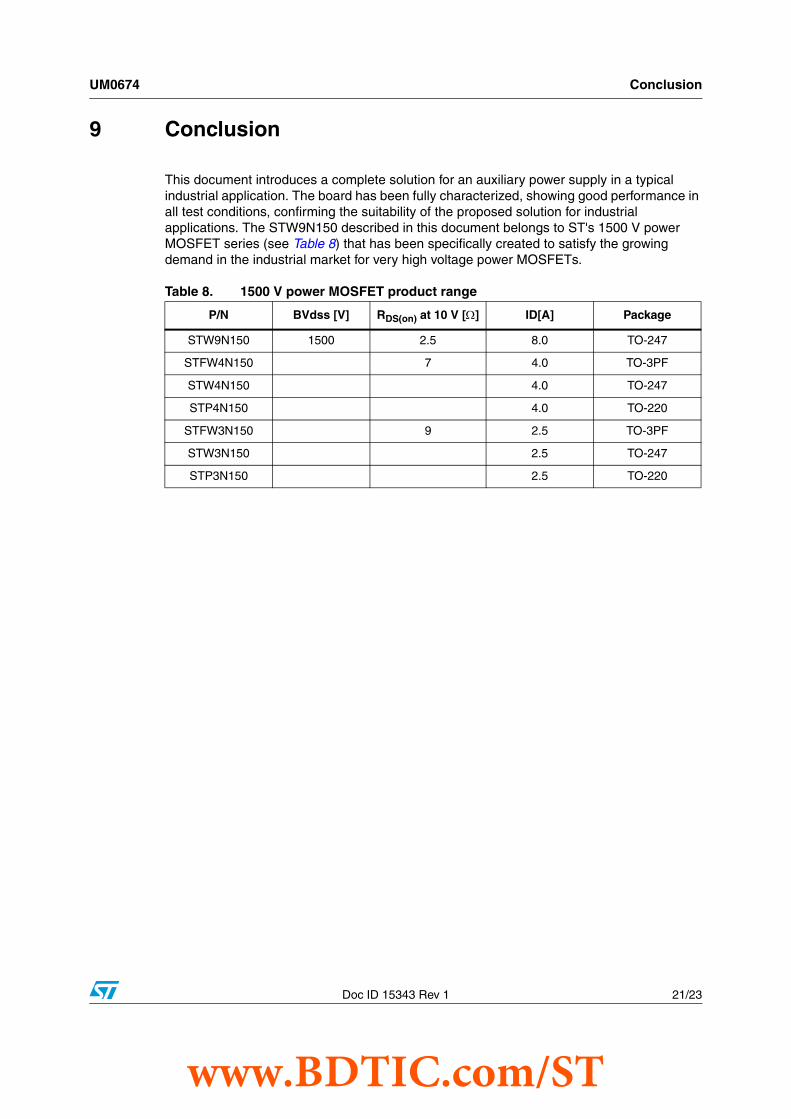
This document introduces a complete solution for an auxiliary power supply in a typical industrial application. The board has been fully characterized, showing good performance in all test conditions, confirming the suitability of the proposed solution for industrial applications. The STW9N150 described in this document belongs to ST's 1500 V power MOSFET series (see Table 8) that has been specifically created to satisfy the growing demand in the industrial market for very high voltage power MOSFETs.
Table 8. 1500 V power MOSFET product range
P/N BVdss [V] RDS(on) at 10 V [Ω] ID[A] Package
STW9N150 1500 2.5 8.0 TO-247
STFW4N150 7 4.0 TO-3PF
STW4N150 4.0 TO-247
STP4N150 4.0 TO-220
STFW3N150 9 2.5 TO-3PF
STW3N150 2.5 TO-247
STP3N150 2.5 TO-220
www.BDTIC.com/ST
Revision history UM0674
22/23 Doc ID 15343 Rev 1
10 Revision history
Table 9. Document revision history
Date Revision Changes
24-Sep-2009 1 Initial release.
www.BDTIC.com/ST
UM0674
Doc ID 15343 Rev 1 23/23
Please Read Carefully:
Information in this document is provided solely in connection with ST products. STMicroelectronics NV and its subsidiaries (“ST”) reserve theright to make changes, corrections, modifications or improvements, to this document, and the products and services described herein at anytime, without notice.
All ST products are sold pursuant to ST’s terms and conditions of sale.
Purchasers are solely responsible for the choice, selection and use of the ST products and services described herein, and ST assumes noliability whatsoever relating to the choice, selection or use of the ST products and services described herein.
No license, express or implied, by estoppel or otherwise, to any intellectual property rights is granted under this document. If any part of thisdocument refers to any third party products or services it shall not be deemed a license grant by ST for the use of such third party productsor services, or any intellectual property contained therein or considered as a warranty covering the use in any manner whatsoever of suchthird party products or services or any intellectual property contained therein.
UNLESS OTHERWISE SET FORTH IN ST’S TERMS AND CONDITIONS OF SALE ST DISCLAIMS ANY EXPRESS OR IMPLIEDWARRANTY WITH RESPECT TO THE USE AND/OR SALE OF ST PRODUCTS INCLUDING WITHOUT LIMITATION IMPLIEDWARRANTIES OF MERCHANTABILITY, FITNESS FOR A PARTICULAR PURPOSE (AND THEIR EQUIVALENTS UNDER THE LAWSOF ANY JURISDICTION), OR INFRINGEMENT OF ANY PATENT, COPYRIGHT OR OTHER INTELLECTUAL PROPERTY RIGHT.
UNLESS EXPRESSLY APPROVED IN WRITING BY AN AUTHORIZED ST REPRESENTATIVE, ST PRODUCTS ARE NOTRECOMMENDED, AUTHORIZED OR WARRANTED FOR USE IN MILITARY, AIR CRAFT, SPACE, LIFE SAVING, OR LIFE SUSTAININGAPPLICATIONS, NOR IN PRODUCTS OR SYSTEMS WHERE FAILURE OR MALFUNCTION MAY RESULT IN PERSONAL INJURY,DEATH, OR SEVERE PROPERTY OR ENVIRONMENTAL DAMAGE. ST PRODUCTS WHICH ARE NOT SPECIFIED AS "AUTOMOTIVEGRADE" MAY ONLY BE USED IN AUTOMOTIVE APPLICATIONS AT USER’S OWN RISK.
Resale of ST products with provisions different from the statements and/or technical features set forth in this document shall immediately voidany warranty granted by ST for the ST product or service described herein and shall not create or extend in any manner whatsoever, anyliability of ST.
ST and the ST logo are trademarks or registered trademarks of ST in various countries.
Information in this document supersedes and replaces all information previously supplied.
The ST logo is a registered trademark of STMicroelectronics. All other names are the property of their respective owners.
© 2009 STMicroelectronics - All rights reserved
STMicroelectronics group of companies
Australia - Belgium - Brazil - Canada - China - Czech Republic - Finland - France - Germany - Hong Kong - India - Israel - Italy - Japan - Malaysia - Malta - Morocco - Philippines - Singapore - Spain - Sweden - Switzerland - United Kingdom - United States of America
www.st.com
www.BDTIC.com/ST


![Winding temperature prediction in split-winding traction transformer · manufactured as seen in the Figure 1 [1] and is usually called a split-winding transformer. The transformer](https://img.pdfslide.net/doc/110x75/60b5dfb61a68b1378b3649a5/winding-temperature-prediction-in-split-winding-traction-transformer-manufactured.jpg)