Embed Size (px)
Citation preview

UM10415EM773 User manualRev. 2 — 7 December 2011 User manual
Document information
Info Content
Keywords Energy metering, ARM Cortex-M0, EM773
Abstract EM773 User manual
NXP Semiconductors UM10415EM773 UM
Revision history
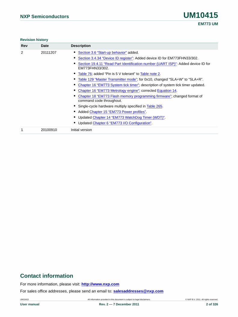
Rev Date Description
2 20111207 • Section 3.6 “Start-up behavior” added.
• Section 3.4.34 “Device ID register”: Added device ID for EM773FHN33/302.
• Section 19.4.11 “Read Part Identification number (UART ISP)”: Added device ID for EM773FHN33/302.
• Table 76; added “Pin is 5 V tolerant” to Table note 2.
• Table 129 “Master Transmitter mode”; for 0x10, changed “SLA+W” to “SLA+R”.
• Chapter 16 “EM773 System tick timer”; description of system tick timer updated.
• Chapter 16 “EM773 Metrology engine”; corrected Equation 14.
• Chapter 18 “EM773 Flash memory programming firmware”; changed format of command code throughout.
• Single-cycle hardware multiply specified in Table 265.
• Added Chapter 15 “EM773 Power profiles”.
• Updated Chapter 14 “EM773 WatchDog Timer (WDT)”.
• Updated Chapter 6 “EM773 I/O Configuration”.
1 20100910 Initial version
UM10415 All information provided in this document is subject to legal disclaimers. © NXP B.V. 2011. All rights reserved.
User manual Rev. 2 — 7 December 2011 2 of 326
Contact informationFor more information, please visit: http://www.nxp.com
For sales office addresses, please send an email to: [email protected]

1.1 Introduction
The EM773 is an ARM Cortex-M0 based, low-cost 32-bit energy metering IC, designed for 8/16-bit smart metering applications. The EM773 offers programmability and on-chip metrology functionality combined with a low power, simple instruction set and memory addressing with reduced code size compared to existing 8/16-bit architectures.
The EM773 operates at CPU frequencies of up to 48 MHz.
The peripheral complement of the EM773 includes up to 32 kB of flash memory, up to 8 kB of data memory, one Fast-mode Plus I2C-bus interface, one RS-485/EIA-485 UART, one SPI interface with SSP features, three general purpose timers, a metrology engine, and up to 25 general purpose I/O pins.
1.2 Features
• System:
– ARM Cortex-M0 processor, running at frequencies of up to 48 MHz.
– ARM Cortex-M0 built-in Nested Vectored Interrupt Controller (NVIC).
– Serial Wire Debug.
– System tick timer.
• Memory:
– 32 kB on-chip flash programming memory.
– 8 kB SRAM.
– In-System Programming (ISP) and In-Application Programming (IAP) via on-chip bootloader software.
• Digital peripherals:
– Up to 25 General Purpose I/O (GPIO) pins with configurable pull-up/pull-down resistors.
– GPIO pins can be used as edge and level sensitive interrupt sources.
– High-current output driver (20 mA) on one pin.
– High-current sink drivers (20 mA) on two I2C-bus pins in Fast-mode Plus.
– Three general purpose timers/counters with a total of two capture inputs and 10 match outputs.
– Programmable WatchDog Timer (WDT).
• Analog peripherals:
– Metrology Engine for Smart Metering with two current inputs and a voltage input.
UM10415Chapter 1: Introductory informationRev. 2 — 7 December 2011 User manual
UM10415 All information provided in this document is subject to legal disclaimers. © NXP B.V. 2011. All rights reserved.
User manual Rev. 2 — 7 December 2011 3 of 326

NXP Semiconductors UM10415Chapter 1: Introductory information
• Serial interfaces:
– UART with fractional baud rate generation, internal FIFO, and RS-485 support.
– One SPI controller with SSP features and with FIFO and multi-protocol capabilities.
– I2C-bus interface supporting full I2C-bus specification and Fast-mode Plus with a data rate of 1 Mbit/s with multiple address recognition and monitor mode.
• Clock generation:
– 12 MHz internal RC oscillator trimmed to 1 % accuracy that can optionally be used as a system clock.
– Crystal oscillator with an operating range of 1 MHz to 25 MHz.
– Programmable watchdog oscillator with a frequency range of 7.8 kHz to 1.8 MHz.
– PLL allows CPU operation up to the maximum CPU rate without the need for a high-frequency crystal. May be run from the system oscillator or the internal RC oscillator.
– Clock output function with divider that can reflect the system oscillator clock, IRC clock, CPU clock, and the Watchdog clock.
• Power control:
– Integrated PMU (Power Management Unit) to minimize power consumption during Sleep, Deep-sleep, and Deep power-down modes.
– Three reduced power modes: Sleep, Deep-sleep, and Deep power-down.
– Processor wake-up from Deep-sleep mode via a dedicated start logic using up to 11 of the functional pins.
– Power-On Reset (POR).
– Brownout detect with four separate thresholds for interrupt and forced reset.
• Unique device serial number for identification.
• Single 3.3 V power supply (1.8 V to 3.6 V).
• Available as 33-pin HVQFN package.
1.3 Ordering information
Table 1. Ordering information
Type number Package
Name Description Version
EM773FHN33 HVQFN33 HVQFN: plastic thermal enhanced very thin quad flat package; no leads; 33 terminals; body 7 x 7 x 0.85 mm
n/a
UM10415 All information provided in this document is subject to legal disclaimers. © NXP B.V. 2011. All rights reserved.
User manual Rev. 2 — 7 December 2011 4 of 326

NXP Semiconductors UM10415Chapter 1: Introductory information
1.4 Block diagram
Fig 1. EM773 block diagram
SRAM8 kB
ARMCORTEX-M0
TEST/DEBUGINTERFACE
FLASH32 kB
HIGH-SPEEDGPIO
AHB TO APBBRIDGE
CLOCKGENERATION,
POWER CONTROL,SYSTEM
FUNCTIONS
XTALINXTALOUT
RESET
clocks and controls
SWD
EM773
002aag726
slave
slave
slave slave
ROM
slave
AHB-LITE BUSGPIO portsPIO0/1/2/3
CLKOUT
IRC
POR
SPI0
METROLOGY ENGINEUART
32-bit COUNTER/TIMER 0
I2C-BUS
WDT
IOCONFIG
CT32B0_MAT[2:0]
I_LOWGAINI_HIGHGAINVOLTAGE
CT32B0_CAP0
SDASCL
RXDTXD
DTR, CTS, RTS
SYSTEM CONTROL
PMU
32-bit COUNTER/TIMER 1CT32B1_MAT[3:0]
16-bit COUNTER/TIMER 0CT16B0_MAT[2:0]
CT16B0_CAP0
SCK0, SSEL0MISO0, MOSI0
system bus
UM10415 All information provided in this document is subject to legal disclaimers. © NXP B.V. 2011. All rights reserved.
User manual Rev. 2 — 7 December 2011 5 of 326

NXP Semiconductors UM10415Chapter 1: Introductory information
1.5 ARM Cortex-M0 processor
The ARM Cortex-M0 processor is described in detail in Section 21.2 “About the Cortex-M0 processor and core peripherals”. For the EM773, the ARM Cortex-M0 processor core is configured as follows:
• System options:
– The Nested Vectored Interrupt Controller (NVIC) is included and supports up to 32 interrupts.
– The system tick timer is included.
• Debug options: Serial Wire Debug is included with two watchpoints and four breakpoints.
UM10415 All information provided in this document is subject to legal disclaimers. © NXP B.V. 2011. All rights reserved.
User manual Rev. 2 — 7 December 2011 6 of 326

2.1 Memory map
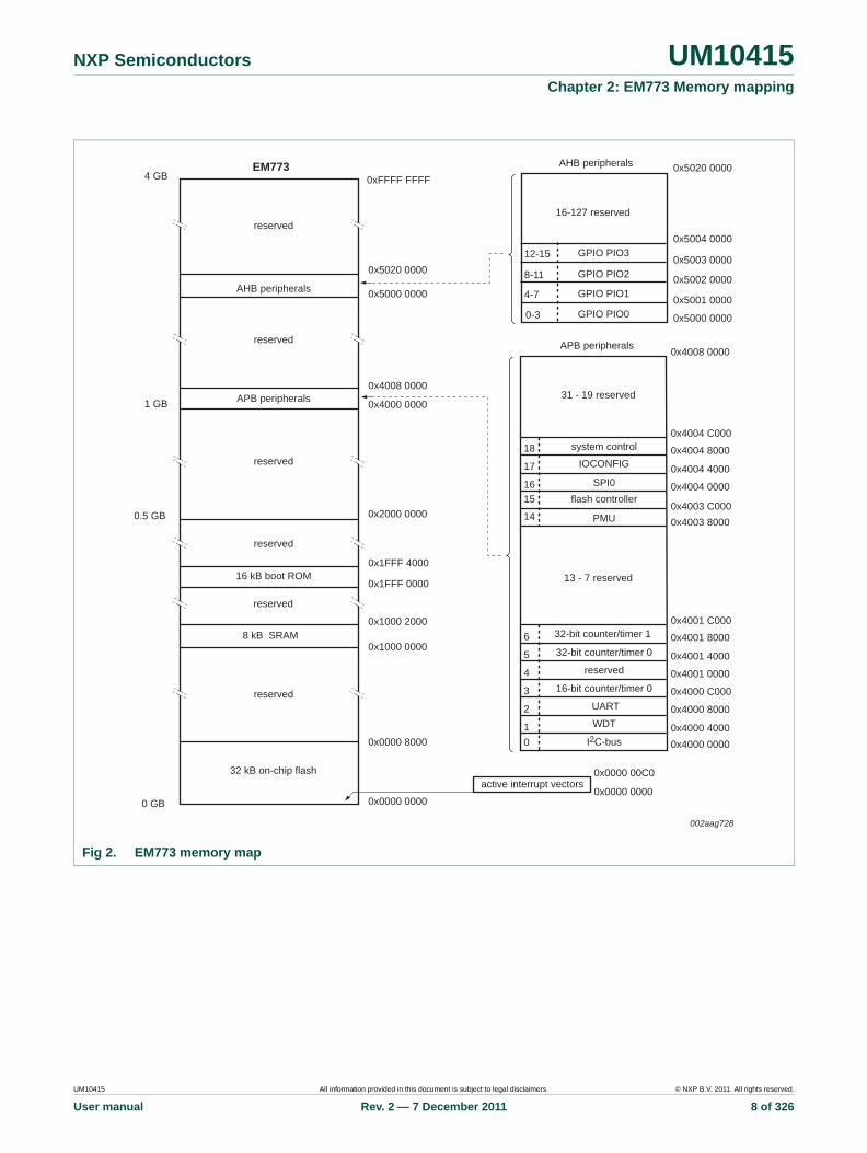
Figure 2 shows the memory and peripheral address space of the EM773.
The AHB peripheral area is 2 MB in size and is divided to allow for up to 128 peripherals. On the EM773, the GPIO ports are the only AHB peripherals. The APB peripheral area is 512 kB in size and is divided to allow for up to 32 peripherals. Each peripheral of either type is allocated 16 kB of space. This allows simplifying the address decoding for each peripheral.
All peripheral register addresses are 32-bit word aligned regardless of their size. An implication of this is that word and half-word registers must be accessed all at once. For example, it is not possible to read or write the upper byte of a word register separately.
UM10415Chapter 2: EM773 Memory mappingRev. 2 — 7 December 2011 User manual
UM10415 All information provided in this document is subject to legal disclaimers. © NXP B.V. 2011. All rights reserved.
User manual Rev. 2 — 7 December 2011 7 of 326
NXP Semiconductors UM10415Chapter 2: EM773 Memory mapping
Fig 2. EM773 memory map
0x5000 0000
0x5001 0000
0x5002 0000
0x5020 0000AHB peripherals
16-127 reserved
GPIO PIO1 4-7
0x5003 0000
0x5004 0000
GPIO PIO2
GPIO PIO3
8-11
12-15
GPIO PIO0 0-3
APB peripherals
0x4000 4000
0x4000 8000
0x4000 C000
0x4001 0000
0x4001 8000
0x4003 80000x4003 C000
0x4004 0000
0x4004 4000
0x4004 8000
0x4004 C000
0x4008 0000
0x4001 C000
0x4001 4000
0x4000 0000
WDT
32-bit counter/timer 0
32-bit counter/timer 1
UART
PMU
I2C-bus
13 - 7 reserved
31 - 19 reserved
01
2
3
4
5
6
1615
14
17
18
reserved
reserved
reserved
0x0000 00000 GB
0.5 GB
4 GB
1 GB
0x1000 2000
0x1FFF 0000
0x1FFF 4000
0x2000 0000
0x4000 0000
0x4008 0000
0x5000 0000
0x5020 0000
0xFFFF FFFF
reserved
reserved
reserved
APB peripherals
AHB peripherals
8 kB SRAM0x1000 0000
EM773
0x0000 8000
32 kB on-chip flash
16 kB boot ROM
0x0000 0000
0x0000 00C0active interrupt vectors
002aag728
SPI0
reserved
16-bit counter/timer 0
IOCONFIG
system control
flash controller
UM10415 All information provided in this document is subject to legal disclaimers. © NXP B.V. 2011. All rights reserved.
User manual Rev. 2 — 7 December 2011 8 of 326

3.1 Introduction
The system configuration block controls oscillators, start logic, and clock generation of the EM773. Also included in this block are registers for setting the priority for AHB access and a register for remapping flash, SRAM, and ROM memory areas.
3.2 Pin description
Table 2 shows pins that are associated with system control block functions.
3.3 Clocking and power control
See Figure 3 for an overview of the EM773 Clock Generation Unit (CGU).
The EM773 includes three independent oscillators. These are the system oscillator, the Internal RC oscillator (IRC), and the watchdog oscillator. Each oscillator can be used for more than one purpose as required in a particular application.
Following reset, the EM773 will operate from the Internal RC oscillator until switched by software. This allows systems to operate without any external crystal and the bootloader code to operate at a known frequency.
The SYSAHBCLKCTRL register gates the system clock to the various peripherals and memories. UART, the WDT, and SPI0 have individual clock dividers to derive peripheral clocks from the main clock.
The main clock and the clock outputs from the IRC, the system oscillator, and the watchdog oscillator can be observed directly on the CLKOUT pin.
For details on power control see Section 3.8.
UM10415Chapter 3: EM773 C_CANRev. 2 — 7 December 2011 User manual
Table 2. Pin summary
Pin name Pin direction Pin description
CLKOUT O Clockout pin
PIO0_0 to PIO0_10 I Start logic wake-up pins port 0
UM10415 All information provided in this document is subject to legal disclaimers. © NXP B.V. 2011. All rights reserved.
User manual Rev. 2 — 7 December 2011 9 of 326

NXP Semiconductors UM10415Chapter 3: EM773 C_CAN
3.4 Register description
All registers, regardless of size, are on word address boundaries. Details of the registers appear in the description of each function.
See Section 3.11 for the flash access timing register, which can be re-configured as part the system setup. This register is not part of the system configuration block.
Fig 3. EM773 CGU block diagram
SYSTEM PLLIRC oscillator
system oscillator
watchdog oscillator
IRC oscillator
watchdog oscillator
MAINCLKSEL(main clock select)
SYSPLLCLKSEL(system PLL clock select)
SYSTEM CLOCKDIVIDER
AHB clock 0(system)
SYSAHBCLKCTRL[1:18](AHB clock enable)
AHB clocks 1 to 18(memoriesand peripherals)
SPI0 PERIPHERALCLOCK DIVIDER SPI0
UART PERIPHERALCLOCK DIVIDER UART
WDT CLOCKDIVIDER WDT
WDTUEN(WDT clock update enable)
watchdog oscillator
IRC oscillatorsystem oscillator CLKOUT PIN CLOCK
DIVIDER CLKOUT pin
CLKOUTUEN(CLKOUT update enable) 002aag729
main clock
system clock
IRC oscillator
18
Table 3. Register overview: system control block (base address 0x4004 8000)
Name Access Address offset Description Reset value
Reference
SYSMEMREMAP R/W 0x000 System memory remap 0x002 Table 4
PRESETCTRL R/W 0x004 Peripheral reset control 0x000 Table 5
SYSPLLCTRL R/W 0x008 System PLL control 0x000 Table 6
SYSPLLSTAT R 0x00C System PLL status 0x000 Table 7
- - 0x010 - 0x01C Reserved - -
SYSOSCCTRL R/W 0x020 System oscillator control 0x000 Table 8
WDTOSCCTRL R/W 0x024 Watchdog oscillator control 0x000 Table 9
IRCCTRL R/W 0x028 IRC control 0x080 Table 10
- - 0x02C Reserved - -
UM10415 All information provided in this document is subject to legal disclaimers. © NXP B.V. 2011. All rights reserved.
User manual Rev. 2 — 7 December 2011 10 of 326

NXP Semiconductors UM10415Chapter 3: EM773 C_CAN
SYSRSTSTAT R 0x030 System reset status register 0x000 Table 11
- - 0x034 - 0x03C Reserved - -
SYSPLLCLKSEL R/W 0x040 System PLL clock source select 0x000 Table 12
SYSPLLCLKUEN R/W 0x044 System PLL clock source update enable 0x000 Table 13
- - 0x048 - 0x06C Reserved - -
MAINCLKSEL R/W 0x070 Main clock source select 0x000 Table 14
MAINCLKUEN R/W 0x074 Main clock source update enable 0x000 Table 15
SYSAHBCLKDIV R/W 0x078 System AHB clock divider 0x001 Table 16
- - 0x07C Reserved - -
SYSAHBCLKCTRL R/W 0x080 System AHB clock control 0x85F Table 17
- - 0x084 - 0x090 Reserved - -
SSP0CLKDIV R/W 0x094 SPI0 clock divider 0x000 Table 18
UARTCLKDIV R/W 0x098 UART clock divider 0x000 Table 19
- - 0x0A0-0x0CC Reserved - -
WDTCLKSEL R/W 0x0D0 WDT clock source select 0x000 Table 20
WDTCLKUEN R/W 0x0D4 WDT clock source update enable 0x000 Table 21
WDTCLKDIV R/W 0x0D8 WDT clock divider 0x000 Table 22
- - 0x0DC Reserved - -
CLKOUTCLKSEL R/W 0x0E0 CLKOUT clock source select 0x000 Table 23
CLKOUTUEN R/W 0x0E4 CLKOUT clock source update enable 0x000 Table 24
CLKOUTDIV R/W 0x0E8 CLKOUT clock divider 0x000 Table 25
- - 0x0EC - 0x0FC Reserved - -
PIOPORCAP0 R 0x100 POR captured PIO status 0 user dependent
Table 26
PIOPORCAP1 R 0x104 POR captured PIO status 1 user dependent
Table 27
- R 0x108 - 0x14C Reserved - -
BODCTRL R/W 0x150 BOD control 0x000 Table 28
- - 0x154 Reserved - -
SYSTCKCAL R/W 0x158 System tick counter calibration 0x004 Table 29
- - 0x15C - 0x1FC Reserved - -
STARTAPRP0 R/W 0x200 Start logic edge control register 0 Table 30
STARTERP0 R/W 0x204 Start logic signal enable register 0 Table 31
STARTRSRP0CLR W 0x208 Start logic reset register 0 n/a Table 32
STARTSRP0 R 0x20C Start logic status register 0 n/a Table 33
- - 0x210 - 0x22C Reserved - -
PDSLEEPCFG R/W 0x230 Power-down states in Deep-sleep mode 0x0000 0000
Table 35
PDAWAKECFG R/W 0x234 Power-down states after wake-up from Deep-sleep mode
0x0000 EDF0
Table 36
Table 3. Register overview: system control block (base address 0x4004 8000) …continued
Name Access Address offset Description Reset value
Reference
UM10415 All information provided in this document is subject to legal disclaimers. © NXP B.V. 2011. All rights reserved.
User manual Rev. 2 — 7 December 2011 11 of 326

NXP Semiconductors UM10415Chapter 3: EM773 C_CAN
3.4.1 System memory remap register
The system memory remap register selects whether the ARM interrupt vectors are read from the boot ROM, the flash, or the SRAM. By default, the flash memory is mapped to address 0x0000 0000. When the MAP bits in the SYSMEMREMAP register are set to 0x0 or 0x1, the boot ROM or RAM respectively are mapped to the bottom 512 bytes of the memory map (addresses 0x0000 0000 to 0x0000 0200).
3.4.2 Peripheral reset control register
This register allows software to reset the SPI and I2C peripherals. Writing a 0 to the SSP0_RST_N or I2C_RST_N bits resets the SPI0 or I2C peripheral. Writing a 1 de-asserts the reset.
Remark: Before accessing the SPI and I2C peripherals, write a 1 to this register to ensure that the reset signals to the SPI and I2C are de-asserted.
PDRUNCFG R/W 0x238 Power-down configuration register 0x0000 EDF0
Table 37
- - 0x23C - 0x3F0 Reserved - -
DEVICE_ID R 0x3F4 Device ID part dependent
Table 38
Table 3. Register overview: system control block (base address 0x4004 8000) …continued
Name Access Address offset Description Reset value
Reference
Table 4. System memory remap register (SYSMEMREMAP, address 0x4004 8000) bit description
Bit Symbol Value Description Reset value
1:0 MAP System memory remap 0x02
00 Boot Loader Mode. Interrupt vectors are re-mapped to Boot ROM.
01 User RAM Mode. Interrupt vectors are re-mapped to Static RAM.
10 or 11
User Flash Mode. Interrupt vectors are not re-mapped and reside in Flash.
31:2 - - Reserved 0x00
Table 5. Peripheral reset control register (PRESETCTRL, address 0x4004 8004) bit description
Bit Symbol Value Description Reset value
0 SSP0_RST_N SPI0 reset control 0
0 Resets the SPI0 peripheral.
1 SPI0 reset de-asserted.
1 I2C_RST_N I2C reset control 0
0 Resets the I2C peripheral.
1 I2C reset de-asserted.
31:2 - - Reserved 0x00
UM10415 All information provided in this document is subject to legal disclaimers. © NXP B.V. 2011. All rights reserved.
User manual Rev. 2 — 7 December 2011 12 of 326

NXP Semiconductors UM10415Chapter 3: EM773 C_CAN
3.4.3 System PLL control register
This register connects and enables the system PLL and configures the PLL multiplier and divider values. The PLL accepts an input frequency from 10 MHz to 25 MHz from various clock sources. The input frequency is multiplied up to a high frequency, then divided down to provide the actual clock used by the CPU, peripherals, and memories. The PLL can produce a clock up to the maximum allowed for the CPU.
3.4.4 System PLL status register
This register is a Read-only register and supplies the PLL lock status (see Section 3.10.1).
3.4.5 System oscillator control register
This register configures the frequency range for the system oscillator.
Table 6. System PLL control register (SYSPLLCTRL, address 0x4004 8008) bit description
Bit Symbol Value Description Reset value
4:0 MSEL Feedback divider value. The division value M is the programmed MSEL value + 1.
0x000
00000 Division ratio M = 1
...
11111 Division ration M = 32
6:5 PSEL Post divider ratio P. The division ratio is 2 P. 0x00
00 P = 1
01 P = 2
10 P = 4
11 P = 8
31:7 - - Reserved. Do not write ones to reserved bits. 0x0
Table 7. System PLL status register (SYSPLLSTAT, address 0x4004 800C) bit description
Bit Symbol Value Description Reset value
0 LOCK PLL lock status 0x0
0 PLL not locked
1 PLL locked
31:1 - - Reserved 0x00
Table 8. System oscillator control register (SYSOSCCTRL, address 0x4004 8020) bit description
Bit Symbol Value Description Reset value
0 BYPASS Bypass system oscillator 0x0
0 Oscillator is not bypassed.
1 Bypass enabled. PLL input (sys_osc_clk) is fed directly from the XTALIN and XTALOUT pins.
UM10415 All information provided in this document is subject to legal disclaimers. © NXP B.V. 2011. All rights reserved.
User manual Rev. 2 — 7 December 2011 13 of 326

NXP Semiconductors UM10415Chapter 3: EM773 C_CAN
3.4.6 Watchdog oscillator control register
This register configures the watchdog oscillator. The oscillator consists of an analog and a digital part. The analog part contains the oscillator function and generates an analog clock (Fclkana). With the digital part, the analog output clock (Fclkana) can be divided to the required output clock frequency wdt_osc_clk. The analog output frequency (Fclkana) can be adjusted with the FREQSEL bits between 500 kHz and 3.4 MHz. With the digital part Fclkana will be divided (divider ratios = 2, 4,...,64) to wdt_osc_clk using the DIVSEL bits.
The output clock frequency of the watchdog oscillator can be calculated as wdt_osc_clk = Fclkana/(2 (1 + DIVSEL)) = 7.8 kHz to 1.7 MHz (nominal values).
Remark: Any setting of the FREQSEL bits will yield a Fclkana value within 40% of the listed frequency value. The watchdog oscillator is the clock source with the lowest power consumption. If accurate timing is required, use the IRC or system oscillator.
Remark: The frequency of the watchdog oscillator is undefined after reset. The watchdog oscillator frequency must be programmed by writing to the WDTOSCCTRL register before using the watchdog oscillator.
1 FREQRANGE Determines frequency range for Low-power oscillator.
0x0
0 1 - 20 MHz frequency range.
1 15 - 25 MHz frequency range
31:2 - - Reserved 0x00
Table 8. System oscillator control register (SYSOSCCTRL, address 0x4004 8020) bit description …continued
Bit Symbol Value Description Reset value
Table 9. Watchdog oscillator control register (WDTOSCCTRL, address 0x4004 8024) bit description
Bit Symbol Value Description Reset value
4:0 DIVSEL Select divider for Fclkana. wdt_osc_clk = Fclkana/(2 (1 + DIVSEL))
0x00
00000 2 (1 + DIVSEL) = 2
00001 2 (1 + DIVSEL) = 4
00010 2 (1 + DIVSEL) = 6
... ...
11111 2 (1 + DIVSEL) = 64
8:5 FREQSEL Select watchdog oscillator analog output frequency (Fclkana).
0x00
0001 0.5 MHz
0010 0.8 MHz
0011 1.1 MHz
0100 1.4 MHz
0101 1.6 MHz
0110 1.8 MHz
UM10415 All information provided in this document is subject to legal disclaimers. © NXP B.V. 2011. All rights reserved.
User manual Rev. 2 — 7 December 2011 14 of 326

NXP Semiconductors UM10415Chapter 3: EM773 C_CAN
3.4.7 Internal resonant crystal control register
This register is used to trim the on-chip 12 MHz oscillator. The trim value is factory-preset and written by the boot code on start-up.
0111 2.0 MHz
1000 2.2 MHz
1001 2.4 MHz
1010 2.6 MHz
1011 2.7 MHz
1100 2.9 MHz
1101 3.1 MHz
1110 3.2 MHz
1111 3.4 MHz
31:9 - - Reserved 0x00
Table 9. Watchdog oscillator control register (WDTOSCCTRL, address 0x4004 8024) bit description …continued
Bit Symbol Value Description Reset value
Table 10. Internal resonant crystal control register (IRCCTRL, address 0x4004 8028) bit description
Bit Symbol Value Description Reset value
7:0 TRIM Trim value 0x1000 0000, then flash will reprogram
31:9 - - Reserved 0x00
UM10415 All information provided in this document is subject to legal disclaimers. © NXP B.V. 2011. All rights reserved.
User manual Rev. 2 — 7 December 2011 15 of 326

NXP Semiconductors UM10415Chapter 3: EM773 C_CAN
3.4.8 System reset status register
The SYSRSTSTAT register shows the source of the latest reset event. The bits are cleared by writing a one to any of the bits. The POR event clears all other bits in this register, but if another reset signal - for example EXTRST - remains asserted after the POR signal is negated, then its bit is set to detected.
3.4.9 System PLL clock source select register
This register selects the clock source for the system PLL. The SYSPLLCLKUEN register (see Section 3.4.10) must be toggled from LOW to HIGH for the update to take effect.
Remark: When switching clock sources, both clocks must be running before the clock source can be updated.
Table 11. System reset status register (SYSRSTSTAT, address 0x4004 8030) bit description
Bit Symbol Value Description Reset value
0 POR POR reset status 0x0
0 no POR detected
1 POR detected
1 EXTRST Status of the external RESET pin 0x0
0 no RESET event detected
1 RESET detected
2 WDT Status of the Watchdog reset 0x0
0 no WDT reset detected
1 WDT reset detected
3 BOD Status of the Brown-out detect reset 0x0
0 no BOD reset detected
1 BOD reset detected
4 SYSRST Status of the software system reset 0x0
0 no System reset detected
1 System reset detected
31:5 - - Reserved 0x00
Table 12. System PLL clock source select register (SYSPLLCLKSEL, address 0x4004 8040) bit description
Bit Symbol Value Description Reset value
1:0 SEL System PLL clock source 0x00
00 IRC oscillator
01 System oscillator
10 Reserved
11 Reserved
31:2 - - Reserved 0x00
UM10415 All information provided in this document is subject to legal disclaimers. © NXP B.V. 2011. All rights reserved.
User manual Rev. 2 — 7 December 2011 16 of 326
NXP Semiconductors UM10415Chapter 3: EM773 C_CAN
3.4.10 System PLL clock source update enable register
This register updates the clock source of the system PLL with the new input clock after the SYSPLLCLKSEL register has been written to. In order for the update to take effect, first write a zero to the SYSPLLUEN register and then write a one to SYSPLLUEN.
To successfully change clock sources, both clock sources must be running before updating this register.
3.4.11 Main clock source select register
This register selects the main system clock which can be either any input to the system PLL, the output from the system PLL (sys_pllclkout), or the watchdog or IRC oscillators directly. The main system clock clocks the core, the peripherals, and the memories.
The MAINCLKUEN register (see Section 3.4.12) must be toggled from LOW to HIGH for the update to take effect.
Remark: When switching clock sources, both clocks must be running before the clock source can be updated.
3.4.12 Main clock source update enable register
This register updates the clock source of the main clock with the new input clock after the MAINCLKSEL register has been written to. In order for the update to take effect, first write a zero to the MAINCLKUEN register and then write a one to MAINCLKUEN.
To successfully change clock sources, both clock sources must be running before updating this register.
Table 13. System PLL clock source update enable register (SYSPLLUEN, address 0x4004 8044) bit description
Bit Symbol Value Description Reset value
0 ENA Enable system PLL clock source update 0x0
0 No change
1 Update clock source
31:1 - - Reserved 0x00
Table 14. Main clock source select register (MAINCLKSEL, address 0x4004 8070) bit description
Bit Symbol Value Description Reset value
1:0 SEL Cock source for main clock 0x00
00 IRC oscillator
01 Input clock to system PLL
10 WDT oscillator
11 System PLL clock out
31:2 - - Reserved 0x00
UM10415 All information provided in this document is subject to legal disclaimers. © NXP B.V. 2011. All rights reserved.
User manual Rev. 2 — 7 December 2011 17 of 326
NXP Semiconductors UM10415Chapter 3: EM773 C_CAN
3.4.13 System AHB clock divider register
This register divides the main clock to provide the system clock to the core, memories, and the peripherals. The system clock can be shut down completely by setting the DIV bits to 0x0.
3.4.14 System AHB clock control register
The AHBCLKCTRL register enables the clocks to individual system and peripheral blocks. The system clock (sys_ahb_clk[0], bit 0 in the AHBCLKCTRL register) provides the clock for the AHB to APB bridge, the AHB matrix, the ARM Cortex-M0, the Syscon block, and the PMU. This clock cannot be disabled.
Table 15. Main clock source update enable register (MAINCLKUEN, address 0x4004 8074) bit description
Bit Symbol Value Description Reset value
0 ENA Enable main clock source update 0x0
0 No change
1 Update clock source
31:1 - - Reserved 0x00
Table 16. System AHB clock divider register (SYSAHBCLKDIV, address 0x4004 8078) bit description
Bit Symbol Value Description Reset value
7:0 DIV System AHB clock divider values 0x01
0 System clock disabled.
1 Divide by 1
to ...
255 Divide by 255
31:8 - - Reserved 0x00
Table 17. System AHB clock control register (SYSAHBCLKCTRL, address 0x4004 8080) bit description
Bit Symbol Value Description Reset value
0 SYS Enables clock for AHB to APB bridge, to the AHB matrix, to the Cortex-M0 FCLK and HCLK, to the SysCon, and to the PMU. This bit is read only.
1
0 Reserved
1 Enable
1 ROM Enables clock for ROM. 1
0 Disable
1 Enable
2 RAM Enables clock for RAM. 1
0 Disable
1 Enable
UM10415 All information provided in this document is subject to legal disclaimers. © NXP B.V. 2011. All rights reserved.
User manual Rev. 2 — 7 December 2011 18 of 326

NXP Semiconductors UM10415Chapter 3: EM773 C_CAN
3 FLASHREG Enables clock for flash register interface. 1
0 Disabled
1 Enabled
4 FLASHARRAY Enables clock for flash array access. 1
0 Disabled
1 Enabled
5 I2C Enables clock for I2C. 0
0 Disable
1 Enable
6 GPIO Enables clock for GPIO. 1
0 Disable
1 Enable
7 CT16B0 Enables clock for 16-bit counter/timer 0. 0
0 Disable
1 Enable
8 Metrology engine clock
Automatically set by the metrology engine software. 0
0 Disable
1 Enable
9 CT32B0 Enables clock for 32-bit counter/timer 0. 0
0 Disable
1 Enable
10 CT32B1 Enables clock for 32-bit counter/timer 1. 0
0 Disable
1 Enable
11 SSP0 Enables clock for SPI0. 1
0 Disable
1 Enable
12 UART Enables clock for UART. 0
0 Disable
1 Enable
13 Metrology engine clock
Automatically set by the metrology engine software. 0
0 Disable
1 Enable
14 - - Reserved 0
15 WDT Enables clock for WDT. 0
0 Disable
1 Enable
Table 17. System AHB clock control register (SYSAHBCLKCTRL, address 0x4004 8080) bit description …continued
Bit Symbol Value Description Reset value
UM10415 All information provided in this document is subject to legal disclaimers. © NXP B.V. 2011. All rights reserved.
User manual Rev. 2 — 7 December 2011 19 of 326
NXP Semiconductors UM10415Chapter 3: EM773 C_CAN
3.4.15 SPI0 clock divider register
This register configures the SPI0 peripheral clock SPI0_PCLK. The SPI0_PCLK can be shut down by setting the DIV bits to 0x0.
3.4.16 UART clock divider register
This register configures the UART peripheral clock UART_PCLK. The UART_PCLK can be shut down by setting the DIV bits to 0x0.
3.4.17 WDT clock source select register
This register selects the clock source for the watchdog timer. The WDTCLKUEN register (see Section 3.4.18) must be toggled from LOW to HIGH for the update to take effect.
16 IOCON Enables clock for I/O configuration block. 0
0 Disable
1 Enable
17 - - Reserved 0
18 - - Reserved 0
31:19 - - Reserved 0x00
Table 17. System AHB clock control register (SYSAHBCLKCTRL, address 0x4004 8080) bit description …continued
Bit Symbol Value Description Reset value
Table 18. SPI0 clock divider register (SSP0CLKDIV, address 0x4004 8094) bit description
Bit Symbol Value Description Reset value
7:0 DIV SPI0_PCLK clock divider values 0x00
0 Disable SPI0_PCLK.
1 Divide by 1.
to ...
255 Divide by 255.
31:8 - - Reserved 0x00
Table 19. UART clock divider register (UARTCLKDIV, address 0x4004 8098) bit description
Bit Symbol Value Description Reset value
7:0 DIV UART_PCLK clock divider values 0x00
0 Disable UART_PCLK.
1 Divide by 1.
to ...
255 Divide by 255.
31:8 - - Reserved 0x00
UM10415 All information provided in this document is subject to legal disclaimers. © NXP B.V. 2011. All rights reserved.
User manual Rev. 2 — 7 December 2011 20 of 326

NXP Semiconductors UM10415Chapter 3: EM773 C_CAN
3.4.18 WDT clock source update enable register
This register updates the clock source of the watchdog timer with the new input clock after the WDTCLKSEL register has been written to. In order for the update to take effect at the input of the watchdog timer, first write a zero to the WDTCLKUEN register and then write a one to WDTCLKUEN.
3.4.19 WDT clock divider register
This register determines the divider values for the watchdog clock wdt_clk.
3.4.20 CLKOUT clock source select register
This register configures the clkout_clk signal to be output on the CLKOUT pin. All three oscillators and the main clock can be selected for the clkout_clk clock.
The CLKOUTCLKUEN register (see Section 3.4.21) must be toggled from LOW to HIGH for the update to take effect.
Table 20. WDT clock source select register (WDTCLKSEL, address 0x4004 80D0) bit description
Bit Symbol Value Description Reset value
1:0 SEL WDT clock source 0x00
00 IRC oscillator
01 Main clock
10 Watchdog oscillator
11 Reserved
31:2 - - Reserved 0x00
Table 21. WDT clock source update enable register (WDTCLKUEN, address 0x4004 80D4) bit description
Bit Symbol Value Description Reset value
0 ENA Enable WDT clock source update 0x0
0 No change
1 Update clock source
31:1 - - Reserved 0x00
Table 22. WDT clock divider register (WDTCLKDIV, address 0x4004 80D8) bit description
Bit Symbol Value Description Reset value
7:0 DIV WDT clock divider values 0x00
0 Disable
1 Divide by 1
to ...
255 Divide by 255
31:8 - - Reserved 0x00
UM10415 All information provided in this document is subject to legal disclaimers. © NXP B.V. 2011. All rights reserved.
User manual Rev. 2 — 7 December 2011 21 of 326

NXP Semiconductors UM10415Chapter 3: EM773 C_CAN
3.4.21 CLKOUT clock source update enable register
This register updates the clock source of the CLKOUT pin with the new clock after the CLKOUTCLKSEL register has been written to. In order for the update to take effect at the input of the CLKOUT pin, first write a zero to the CLKCLKUEN register and then write a one to CLKCLKUEN.
3.4.22 CLKOUT clock divider register
This register determines the divider value for the clock output signal on the CLKOUT pin.
3.4.23 POR captured PIO status register 0
The PIOPORCAP0 register captures the state (HIGH or LOW) of the PIO pins of ports 0,1, and 2 (pins PIO2_0 to PIO2_7) at power-on-reset. Each bit represents the reset state of one GPIO pin. This register is a read-only status register.
Table 23. CLKOUT clock source select register (CLKOUTCLKSEL, address 0x4004 80E0) bit description
Bit Symbol Value Description Reset value
1:0 SEL CLKOUT clock source 0x00
00 IRC oscillator
01 System oscillator
10 Watchdog oscillator
11 Main clock
31:2 - - Reserved 0x00
Table 24. CLKOUT clock source update enable register (CLKOUTUEN, address 0x4004 80E4) bit description
Bit Symbol Value Description Reset value
0 ENA Enable CLKOUT clock source update 0x0
0 No change
1 Update clock source
31:1 - - Reserved 0x00
Table 25. CLKOUT clock divider registers (CLKOUTCLKDIV, address 0x4004 80E8) bit description
Bit Symbol Value Description Reset value
7:0 DIV Clock divider values 0x00
0 Disable
1 Divide by 1
to ...
255 Divide by 255
31:8 - - Reserved 0x00
UM10415 All information provided in this document is subject to legal disclaimers. © NXP B.V. 2011. All rights reserved.
User manual Rev. 2 — 7 December 2011 22 of 326
NXP Semiconductors UM10415Chapter 3: EM773 C_CAN
3.4.24 POR captured PIO status register 1
The PIOPORCAP1 register captures the state (HIGH or LOW) of the PIO pins of port 2 (PIO2_8 to PIO2_11) and port 3 at power-on-reset. Each bit represents the reset state of one PIO pin. This register is a read-only status register.
3.4.25 BOD control register
The BOD control register selects four separate threshold values for sending a BOD interrupt to the NVIC and for forced reset. Reset and interrupt threshold values listed in Table 28 are typical values.
Table 26. POR captured PIO status registers 0 (PIOPORCAP0, address 0x4004 8100) bit description
Bit Symbol Description Reset value
11:0 CAPPIO0_11 to CAPPIO0_0
Raw reset status input PIO0_11 to PIO0_0
User implementation dependent
23:12 CAPPIO1_11 to CAPPIO1_0
Raw reset status input PIO1_11 to PIO1_0
User implementation dependent
31:24 CAPPIO2_7 to CAPPIO2_0
Raw reset status input PIO2_7 to PIO2_0
User implementation dependent
Table 27. POR captured PIO status registers 1 (PIOPORCAP1, address 0x4004 8104) bit description
Bit Symbol Description Reset value
0 CAPPIO2_8 Raw reset status input PIO2_8 User implementation dependent
1 CAPPIO2_9 Raw reset status input PIO2_9 User implementation dependent
2 CAPPIO2_10 Raw reset status input PIO2_10 User implementation dependent
3 CAPPIO2_11 Raw reset status input PIO2_11 User implementation dependent
4 CAPPIO3_0 Raw reset status input PIO3_0 User implementation dependent
5 CAPPIO3_1 Raw reset status input PIO3_1 User implementation dependent
6 CAPPIO3_2 Raw reset status input PIO3_2 User implementation dependent
7 CAPPIO3_3 Raw reset status input PIO3_3 User implementation dependent
8 CAPPIO3_4 Raw reset status input PIO3_4 User implementation dependent
9 CAPPIO3_5 Raw reset status input PIO3_5 User implementation dependent
31:10 - Reserved -
Table 28. BOD control register (BODCTRL, address 0x4004 8150) bit description
Bit Symbol Value Description Reset value
1:0 BODRSTLEV BOD reset level 00
00 Level 0: The reset assertion threshold voltage is 1.46 V; the reset de-assertion threshold voltage is 1.63 V.
01 Level 1: The reset assertion threshold voltage is 2.06 V; the reset de-assertion threshold voltage is 2.15 V.
10 Level 2: The reset assertion threshold voltage is 2.35 V; the reset de-assertion threshold voltage is 2.43 V.
11 Level 3: The reset assertion threshold voltage is 2.63 V; the reset de-assertion threshold voltage is 2.71 V.
UM10415 All information provided in this document is subject to legal disclaimers. © NXP B.V. 2011. All rights reserved.
User manual Rev. 2 — 7 December 2011 23 of 326
NXP Semiconductors UM10415Chapter 3: EM773 C_CAN
3.4.26 System tick counter calibration register
3.4.27 Start logic edge control register 0
The STARTAPRP0 register controls the start logic inputs of port 0 (PIO0_0 to PIO0_10). This register selects a falling or rising edge on the corresponding PIO input to produce a falling or rising clock edge, respectively, for the start logic (see Section 3.9.2).
Every bit in the STARTAPRP0 register controls one port input and is connected to one wake-up interrupt in the NVIC. Bit 0 in the STARTAPRP0 register corresponds to interrupt 0, bit 1 to interrupt 1, etc. (see Table 46), up to a total of 11 interrupts.
Remark: Each interrupt connected to a start logic input must be enabled in the NVIC if the corresponding PIO pin is used to wake up the chip from Deep-sleep mode.
3:2 BODINTVAL BOD interrupt level 00
00 Level 0: The interrupt assertion threshold voltage is 1.65 V; the interrupt de-assertion threshold voltage is 1.80 V.
01 Level 1:The interrupt assertion threshold voltage is 2.22 V; the interrupt de-assertion threshold voltage is 2.35 V.
10 Level 2: The interrupt assertion threshold voltage is 2.52 V; the interrupt de-assertion threshold voltage is 2.66 V.
11 Level 3: The interrupt assertion threshold voltage is 2.80 V; the interrupt de-assertion threshold voltage is 2.90 V.
4 BODRSTENA BOD reset enable 0
0 Disable reset function.
1 Enable reset function.
31:5 - - Reserved 0x00
Table 28. BOD control register (BODCTRL, address 0x4004 8150) bit description
Bit Symbol Value Description Reset value
Table 29. System tick timer calibration register (SYSTCKCAL, address 0x4004 8158) bit description
Bit Symbol Value Description Reset value
25:0 CAL System tick timer calibration value 0x04
31:26 - - Reserved 0x00
Table 30. Start logic edge control register 0 (STARTAPRP0, address 0x4004 8200) bit description
Bit Symbol Value Description Reset value
10:0 APRPIO0_10 to APRPIO0_0
Edge select for start logic input PIO0_10 to PIO0_0 0x0
0 Falling edge
1 Rising edge
31:11 - - Reserved. Do not write a 1 to reserved bits in this register.
0x0
UM10415 All information provided in this document is subject to legal disclaimers. © NXP B.V. 2011. All rights reserved.
User manual Rev. 2 — 7 December 2011 24 of 326

NXP Semiconductors UM10415Chapter 3: EM773 C_CAN
3.4.28 Start logic signal enable register 0
This STARTERP0 register enables or disables the start signal bits in the start logic. The bit assignment is identical to Table 30.
3.4.29 Start logic reset register 0
Writing a one to a bit in the STARTRSRP0CLR register resets the start logic state. The bit assignment is identical to Table 30. The start-up logic uses the input signals to generate a clock edge for registering a start signal. This clock edge (falling or rising) sets the interrupt for waking up from Deep-sleep mode. Therefore, the start-up logic states must be cleared before being used.
3.4.30 Start logic status register 0
This register reflects the status of the enabled start signal bits. The bit assignment is identical to Table 30. Each bit (if enabled) reflects the state of the start logic, i.e. whether or not a wake-up signal has been received for a given pin.
Table 31. Start logic signal enable register 0 (STARTERP0, address 0x4004 8204) bit description
Bit Symbol Value Description Reset value
10:0 ERPIO0_10 to ERPIO0_0
Enable start signal for start logic input PIO0_10 to PIO0_0
0x0
0 Disabled
1 Enabled
31:11 - Reserved. Do not write a 1 to reserved bits in this register.
0x0
Table 32. Start logic reset register 0 (STARTRSRP0CLR, address 0x4004 8208) bit description
Bit Symbol Value Description Reset value
10:0 RSRPIO0_10 to RSRPIO0_0
Start signal reset for start logic input PIO0_10 to PIO0_0
n/a
0 -
1 Write: reset start signal
31:11 - - Reserved. Do not write a 1 to reserved bits in this register.
n/a
Table 33. Start logic status register 0 (STARTSRP0, address 0x4004 820C) bit description
Bit Symbol Value Description Reset value
10:0 SRPIO0_10 to SRPIO0_0
Start signal status for start logic input PIO0_10 to PIO0_0
n/a
0 No start signal received
1 Start signal pending
31:11 - - Reserved. Do not write a 1 to reserved bits in this register.
n/a
UM10415 All information provided in this document is subject to legal disclaimers. © NXP B.V. 2011. All rights reserved.
User manual Rev. 2 — 7 December 2011 25 of 326

NXP Semiconductors UM10415Chapter 3: EM773 C_CAN
3.4.31 Deep-sleep mode configuration register
This register controls the behavior of the WatchDog (WD) oscillator and the BOD circuit when the device enters Deep-sleep mode.
This register must be initialized at least once before entering Deep-sleep mode with one of the four values shown in Table 34:
Remark: Failure to initialize and program this register correctly may result in undefined behavior of the microcontroller. The values listed in Table 34 are the only values allowed for PDSLEEPCFG register.
To select the appropriate power configuration for Deep-sleep mode, consider the following:
• BOD: Leaving the BOD circuit enabled will protect the part from a low voltage event occurring while the part is in Deep-sleep mode. However, the BOD circuit causes an additional current drain in Deep-sleep mode.
• WD oscillator: The watchdog oscillator can be left running in Deep-sleep mode to provide a clock for the watchdog timer or a general purpose timer if they are needed for timing a wake-up event (see Section 3.9.3 for details). In this case, the watchdog oscillator analog output frequency must be set to its lowest value (bits FREQSEL in the WDTOSCCTRL = 0001, see Table 9) and all peripheral clocks other than the timer clock must be disabled in the SYSAHBCLKCTRL register (see Table 17) before entering Deep-sleep mode.
The watchdog oscillator, if running, contributes an additional current drain in Deep-sleep mode.
Table 34. Allowed values for PDSLEEPCFG register
Configuration WD oscillator on WD oscillator off
BOD on PDSLEEPCFG = 0x0000 18B7 PDSLEEPCFG = 0x0000 18F7
BOD off PDSLEEPCFG = 0x0000 18BF PDSLEEPCFG = 0x0000 18FF
UM10415 All information provided in this document is subject to legal disclaimers. © NXP B.V. 2011. All rights reserved.
User manual Rev. 2 — 7 December 2011 26 of 326

NXP Semiconductors UM10415Chapter 3: EM773 C_CAN
Remark: Reserved bits in this register must always be written as indicated. This register must be initialized correctly before entering Deep-sleep mode.
3.4.32 Wake-up configuration register
The bits in this register determine the state the chip enters when it is waking up from Deep-sleep mode.
By default, the IRC and flash memory are powered and running and the BOD circuit is enabled when the chip wakes up from Deep-sleep mode.
Remark: Reserved bits must be always written as indicated.
Table 35. Deep-sleep configuration register (PDSLEEPCFG, address 0x4004 8230) bit description
Bit Symbol Value Description Reset value
2:0 - 111 Reserved. Always write these bits as 111. 0
3 BOD_PD BOD power-down control in Deep-sleep mode, see Table 34.
0
0 Powered
1 Powered down
5:4 - 11 Reserved. Always write these bits as 11. 0
6 WDTOSC_PD Watchdog oscillator power control in Deep-sleep mode, see Table 34.
0
0 Powered
1 Powered down
7 - 1 Reserved. Always write this bit as 1. 0
10:8 - 000 Reserved. Always write these bits as 000. 0
12:11 - 11 Reserved. Always write these bits as 11. 0
31:13 - 0 Reserved 0
Table 36. Wake-up configuration register (PDAWAKECFG, address 0x4004 8234) bit description
Bit Symbol Value Description Reset value
0 IRCOUT_PD IRC oscillator output wake-up configuration 0
0 Powered
1 Powered down
1 IRC_PD IRC oscillator power-down wake-up configuration 0
0 Powered
1 Powered down
2 FLASH_PD Flash wake-up configuration 0
0 Powered
1 Powered down
3 BOD_PD BOD wake-up configuration 0
0 Powered
1 Powered down
UM10415 All information provided in this document is subject to legal disclaimers. © NXP B.V. 2011. All rights reserved.
User manual Rev. 2 — 7 December 2011 27 of 326

NXP Semiconductors UM10415Chapter 3: EM773 C_CAN
3.4.33 Power-down configuration register
The bits in the PDRUNCFG register control the power to the various analog blocks. This register can be written to at any time while the chip is running, and a write will take effect immediately with the exception of the power-down signal to the IRC.
To avoid glitches when powering down the IRC, the IRC clock is automatically switched off at a clean point. Therefore, for the IRC a delay is possible before the power-down state takes effect.
By default, the IRC and flash memory are powered and running and the BOD circuit is enabled.
Remark: Reserved bits must be always written as indicated.
4 METENG_PD Metrology Engine wake-up configuration 1
0 Powered
1 Powered down
5 SYSOSC_PD System oscillator wake-up configuration 1
0 Powered
1 Powered down
6 WDTOSC_PD Watchdog oscillator wake-up configuration 1
0 Powered
1 Powered down
7 SYSPLL_PD System PLL wake-up configuration 1
0 Powered
1 Powered down
8 - 1 Reserved. Always write this bit as 1. 1
9 - 0 Reserved. Always write this bit as 0. 0
10 - 1 Reserved. Always write this bit as 1. 1
11 - 1 Reserved. Always write this bit as 1. 1
12 - 0 Reserved. Always write this bit as 0. 0
15:13 - 111 Reserved. Always write these bits as 111. 111
31:16 - - Reserved -
Table 36. Wake-up configuration register (PDAWAKECFG, address 0x4004 8234) bit description …continued
Bit Symbol Value Description Reset value
Table 37. Power-down configuration register (PDRUNCFG, address 0x4004 8238) bit description
Bit Symbol Value Description Reset value
0 IRCOUT_PD IRC oscillator output power-down 0
0 Powered
1 Powered down
UM10415 All information provided in this document is subject to legal disclaimers. © NXP B.V. 2011. All rights reserved.
User manual Rev. 2 — 7 December 2011 28 of 326

NXP Semiconductors UM10415Chapter 3: EM773 C_CAN
3.4.34 Device ID register
This device ID register is a read-only register and contains the part ID for the EM773. This register is also read by the ISP/IAP commands (Section 19.4.11).
1 IRC_PD IRC oscillator power-down 0
0 Powered
1 Powered down
2 FLASH_PD Flash power-down 0
0 Powered
1 Powered down
3 BOD_PD BOD power-down 0
0 Powered
1 Powered down
4 METENG_PD Metrology Engine power-down 1
0 Powered
1 Powered down
5 SYSOSC_PD System oscillator power-down 1
0 Powered
1 Powered down
6 WDTOSC_PD Watchdog oscillator power-down 1
0 Powered
1 Powered down
7 SYSPLL_PD System PLL power-down 1
0 Powered
1 Powered down
8 - 1 Reserved. Always write this bit as 1. 1
9 - 0 Reserved. Always write this bit as 0. 0
10 - 1 Reserved. Always write this bit as 1. 1
11 - 1 Reserved. Always write this bit as 1. 1
12 - 0 Reserved. Always write this bit as 0. 0
15:13 - 111 Reserved. Always write these bits as 111. 111
31:16 - - Reserved -
Table 37. Power-down configuration register (PDRUNCFG, address 0x4004 8238) bit description …continued
Bit Symbol Value Description Reset value
Table 38. Device ID register (DEVICE_ID, address 0x4004 83F4) bit description
Bit Symbol Value Description Reset value
31:0 DEVICEID Part ID number for EM773 part-dependent
0x0444 102B for EM773FHN33/301
0x2540 102B for EM773FHN33/302
UM10415 All information provided in this document is subject to legal disclaimers. © NXP B.V. 2011. All rights reserved.
User manual Rev. 2 — 7 December 2011 29 of 326
NXP Semiconductors UM10415Chapter 3: EM773 C_CAN
3.5 Reset
Reset has four sources on the EM773: the RESET pin, Watchdog Reset, Power-On Reset (POR), and Brown Out Detect (BOD). In addition, there is an ARM software reset.
The RESET pin is a Schmitt trigger input pin. Assertion of chip Reset by any source, once the operating voltage attains a usable level, starts the IRC causing reset to remain asserted until the external Reset is de-asserted, the oscillator is running, and the flash controller has completed its initialization.
On the assertion of any reset source (software reset, POR, BOD reset, External reset, and Watchdog reset), the following processes are initiated:
1. The IRC starts up. After the IRC-start-up time (maximum of 6 s on power-up), the IRC provides a stable clock output.
2. The boot code in the ROM starts. The boot code performs the boot tasks and may jump to the flash.
3. The flash is powered up. This takes approximately 100 s. Then the flash initialization sequence is started, which takes about 250 cycles.
When the internal Reset is removed, the processor begins executing at address 0, which is initially the Reset vector mapped from the boot block. At that point, all of the processor and peripheral registers have been initialized to predetermined values.
3.6 Start-up behavior
See Figure 4 for the start-up timing after reset. The IRC is the default clock at Reset and provides a clean system clock shortly afer the supply voltage reaches the threshold value of 1.8 V.
UM10415 All information provided in this document is subject to legal disclaimers. © NXP B.V. 2011. All rights reserved.
User manual Rev. 2 — 7 December 2011 30 of 326

NXP Semiconductors UM10415Chapter 3: EM773 C_CAN
3.7 Brown-out detection
The EM773 includes four levels for monitoring the voltage on the VDD pin. If this voltage falls below one of the four selected levels, the BOD asserts an interrupt signal to the NVIC. This signal can be enabled for interrupt in the Interrupt Enable Register in the NVIC in order to cause a CPU interrupt; if not, software can monitor the signal by reading the NVIC status register (see Table 46). An additional four threshold levels can be selected to cause a forced reset of the chip (see Table 28).
3.8 Power management
The EM773 supports a variety of power control features. In Active mode, when the chip is running, power and clocks to selected peripherals can be optimized for power consumption. In addition, there are three special modes of processor power reduction: Sleep mode, Deep-sleep mode, and Deep power-down mode.
Remark: The Debug mode is not supported in Sleep, Deep-sleep, or Deep power-down modes.
3.8.1 Active mode
In Active mode, the ARM Cortex-M0 core and memories are clocked by the system clock, and peripherals are clocked by the system clock or a dedicated peripheral clock.
Fig 4. Start-up timing
valid threshold = 1.8V
processor status
VDD
IRC status
RESET
GND
80 μs 101 μs
boot time
user code
boot codeexecutionfinishes;
user code starts
IRCstarts
supply ramp-uptime
55 μs
UM10415 All information provided in this document is subject to legal disclaimers. © NXP B.V. 2011. All rights reserved.
User manual Rev. 2 — 7 December 2011 31 of 326

NXP Semiconductors UM10415Chapter 3: EM773 C_CAN
The chip is in Active mode after reset and the default power configuration is determined by the reset values of the PDRUNCFG and SYSAHBCLKCTRL registers. The power configuration can be changed during run time.
3.8.1.1 Power configuration in Active mode
Power consumption in Active mode is determined by the following configuration choices:
• The SYSAHBCLKCTRL register controls which memories and peripherals are running (Table 17).
• The power to various analog blocks (PLL, oscillators, the BOD circuit, and the flash block) can be controlled at any time individually through the PDRUNCFG register (Table 37).
• The clock source for the system clock can be selected from the IRC (default), the system oscillator, or the watchdog oscillator (see Figure 3 and related registers).
• The system clock frequency can be selected by the SYSPLLCTRL (Table 6) and the SYSAHBCLKDIV register (Table 16).
• Selected peripherals (UART, SPI0, WDT) use individual peripheral clocks with their own clock dividers. The peripheral clocks can be shut down through the corresponding clock divider registers (Table 18 to Table 19).
3.8.2 Sleep mode
In Sleep mode, the system clock to the ARM Cortex-M0 core is stopped, and execution of instructions is suspended until either a reset or an interrupt occurs.
Peripheral functions, if selected to be clocked in the SYSAHBCLKCTRL register, continue operation during Sleep mode and may generate interrupts to cause the processor to resume execution. Sleep mode eliminates dynamic power used by the processor itself, memory systems and related controllers, and internal buses. The processor state and registers, peripheral registers, and internal SRAM values are maintained, and the logic levels of the pins remain static.
3.8.2.1 Power configuration in Sleep mode
Power consumption in Sleep mode is configured by the same settings as in Active mode:
• The clock remains running.
• The system clock frequency remains the same as in Active mode, but the processor is not clocked.
• Analog and digital peripherals are selected as in Active mode.
3.8.2.2 Programming Sleep mode
The following steps must be performed to enter Sleep mode:
1. The DPDEN bit in the PCON register must be set to zero (Table 43).
2. The SLEEPDEEP bit in the ARM Cortex-M0 SCR register must be set to zero, see (Table 255).
3. Use the ARM Cortex-M0 Wait-For-Interrupt (WFI) instruction.
UM10415 All information provided in this document is subject to legal disclaimers. © NXP B.V. 2011. All rights reserved.
User manual Rev. 2 — 7 December 2011 32 of 326

NXP Semiconductors UM10415Chapter 3: EM773 C_CAN
3.8.2.3 Wake-up from Sleep mode
Sleep mode is exited automatically when an interrupt enabled by the NVIC arrives at the processor or a reset occurs. After wake-up due to an interrupt, the microcontroller returns to its original power configuration defined by the contents of the PDRUNCFG and the SYSAHBCLKDIV registers. If a reset occurs, the microcontroller enters the default configuration in Active mode.
3.8.3 Deep-sleep mode
In Deep-sleep mode, the system clock to the processor is disabled as in Sleep mode. All analog blocks are powered down, except for the BOD circuit and the watchdog oscillator, which must be selected or deselected during Deep-sleep mode in the PDSLEEPCFG register.
Deep-sleep mode eliminates all power used by the flash and analog peripherals and all dynamic power used by the processor itself, memory systems and related controllers, and internal buses. The processor state and registers, peripheral registers, and internal SRAM values are maintained, and the logic levels of the pins remain static.
3.8.3.1 Power configuration in Deep-sleep mode
Power consumption in Deep-sleep mode is determined by the Deep-sleep power configuration setting in the PDSLEEPCFG (Table 35) register:
• The only clock source available in Deep-sleep mode is the watchdog oscillator. The watchdog oscillator can be left running in Deep-sleep mode if required for timer-controlled wake-up (see Section 3.9.3). All other clock sources (the IRC and system oscillator) and the system PLL are shut down. The watchdog oscillator analog output frequency must be set to the lowest value of its analog cock output (bits FREQSEL in the WDTOSCCTRL = 0001, see Table 9).
• The BOD circuit can be left running in Deep-sleep mode if required by the application.
• If the watchdog oscillator is running in Deep-sleep mode, only the watchdog timer or one of the general-purpose timers should be enabled in SYSAHBCLKCTRL register to minimize power consumption.
3.8.3.2 Programming Deep-sleep mode
The following steps must be performed to enter Deep-sleep mode:
1. The DPDEN bit in the PCON register must be set to zero (Table 43).
2. Select the power configuration in Deep-sleep mode in the PDSLEEPCFG (Table 35) register.
a. If a timer-controlled wake-up is needed, ensure that the watchdog oscillator is powered in the PDRUNCFG register and switch the clock source to WD oscillator in the MAINCLKSEL register (Table 14).
b. If no timer-controlled wake-up is needed and the watchdog oscillator is shut down, ensure that the IRC is powered in the PDRUNCFG register and switch the clock source to IRC in the MAINCLKSEL register (Table 14). This ensures that the system clock is shut down glitch-free.
3. Select the power configuration after wake-up in the PDAWAKECFG (Table 36) register.
UM10415 All information provided in this document is subject to legal disclaimers. © NXP B.V. 2011. All rights reserved.
User manual Rev. 2 — 7 December 2011 33 of 326

NXP Semiconductors UM10415Chapter 3: EM773 C_CAN
4. If an external pin is used for wake-up, enable and clear the wake-up pin in the start logic registers (Table 30 to Table 33), and enable the start logic interrupt in the NVIC.
5. In the SYSAHBCLKCTRL register (Table 17), disable all peripherals except counter/timer or WDT if needed.
6. Write one to the SLEEPDEEP bit in the ARM Cortex-M0 SCR register (Table 255).
7. Use the ARM WFI instruction.
3.8.3.3 Wake-up from Deep-sleep mode
The microcontroller can wake up from Deep-sleep mode in the following ways:
• Signal on an external pin. For this purpose, pins PIO0_0 to PIO0_11 and PIO1_0 can be enabled as inputs to the start logic. The start logic does not require any clocks and generates the interrupt if enabled in the NVIC to wake up from Deep-sleep mode.
• Input signal to the start logic created by a match event on one of the general purpose timer match outputs. The pin holding the timer match function must be enabled as start logic input in the NVIC, the corresponding timer must be enabled in the SYSAHBCLKCTRL register, and the watchdog oscillator must be running in Deep-sleep mode (for details see Section 3.9.3).
• Reset from the BOD circuit. In this case, the BOD circuit must be enabled in the PDSLEEPCFG register, and the BOD reset must be enabled in the BODCTRL register (Table 28).
• Reset from the watchdog timer. In this case, the watchdog oscillator must be running in Deep-sleep mode (see PDSLEEPCFG register), and the WDT must be enabled in the SYSAHBCLKCTRL register.
Remark: If the watchdog oscillator is running in Deep-sleep mode, its frequency determines the wake-up time causing the wake-up time to be longer than waking up with the IRC.
3.8.4 Deep power-down mode
In Deep power-down mode, power and clocks are shut off to the entire chip with the exception of the WAKEUP pin.
During Deep power-down mode, the contents of the SRAM and registers are not retained except for a small amount of data which can be stored in the general purpose registers of the PMU block.
All functional pins are tri-stated in Deep power-down mode except for the WAKEUP pin.
3.8.4.1 Power configuration in Deep power-down mode
Deep power-down mode has no configuration options. All clocks, the core, and all peripherals are powered down. Only the WAKEUP pin is powered.
3.8.4.2 Programming Deep power-down mode
The following steps must be performed to enter Deep power-down mode:
1. Write one to the DPDEN bit in the PCON register (see Table 43).
2. Store data to be retained in the general purpose registers (Table 44).
UM10415 All information provided in this document is subject to legal disclaimers. © NXP B.V. 2011. All rights reserved.
User manual Rev. 2 — 7 December 2011 34 of 326
NXP Semiconductors UM10415Chapter 3: EM773 C_CAN
3. Write one to the SLEEPDEEP bit in the ARM Cortex-M0 SCR register (Table 255).
4. Use the ARM WFI instruction.
Remark: The WAKEUP pin must be pulled HIGH externally before entering Deep power-down mode.
3.8.4.3 Wake-up from Deep power-down mode
Pulling the WAKEUP pin LOW wakes up the device from Deep power-down, and the chip goes through the entire reset process (Section 3.5). The minimum pulse width for the HIGH-to-LOW transition on the WAKEUP pin is 50 ns.
Follow these steps to wake up the chip from Deep power-down mode:
1. A wake-up signal is generated when a HIGH-to-LOW transition occurs externally on the WAKEUP pin with a pulse length of at least 50 ns while the part is in Deep power-down mode.
– The PMU will turn on the on-chip voltage regulator. When the core voltage reaches the power-on-reset (POR) trip point, a system reset will be triggered and the chip re-boots.
– All registers except the GPREG0 to GPREG4and PCON will be in their reset state.
2. Once the chip has booted, read the deep power-down flag in the PCON register (Table 43) to verify that the reset was caused by a wake-up event from Deep power-down.
3. Clear the deep power-down flag in the PCON register (Table 43).
4. (Optional) Read the stored data in the general purpose registers (Table 44 and Table 45).
5. Set up the PMU for the next Deep power-down cycle.
Remark: The RESET pin has no functionality in Deep power-down mode.
3.9 Deep-sleep mode details
3.9.1 IRC oscillator
The IRC is the only oscillator on the EM773 that can always shut down glitch-free. Therefore it is recommended that the user switches the clock source to IRC before the chip enters Deep-sleep mode.
3.9.2 Start logic
The Deep-sleep mode is exited when the start logic indicates an interrupt to the ARM core. The port pins PIO0_0 to PIO0_10 are connected to the start logic and serve as wake-up pins. The user must program the start logic registers for each input to set the appropriate edge polarity for the corresponding wake-up event. Furthermore, the interrupts corresponding to each input must be enabled in the NVIC. Interrupts 0 to 10 in the NVIC correspond to 11 PIO pins (see Section 3.4.27).
The start logic does not require a clock to run because it uses the input signals on the enabled pins to generate a clock edge when enabled. Therefore, the start logic signals should be cleared (see Table 32) before use.
UM10415 All information provided in this document is subject to legal disclaimers. © NXP B.V. 2011. All rights reserved.
User manual Rev. 2 — 7 December 2011 35 of 326

NXP Semiconductors UM10415Chapter 3: EM773 C_CAN
The start logic can also be used in Active mode to provide a vectored interrupt using the EM773’s input pins.
3.9.3 Using the general purpose counter/timers to create a self-wake-up event
If enabled in Deep-sleep mode through the SYSAHBCLKCFG register, the counter/timers can count clock cycles of the watchdog oscillator and create a match event when the number of cycles equals a preset match value. The match event causes the corresponding match output pin to go HIGH, LOW, or toggle. The state of the match output pin is also monitored by the start logic and can trigger a wake-up interrupt if that pin is enabled in the NVIC and the start logic trigger is configured accordingly in the start logic edge control register (see Table 30).
The following steps must be performed to configure the counter/timer and create a timed Deep-sleep self-wake-up event:
1. Configure the port pin as match output in the IOCONFIG block. Select from pins PIO0_1 or PIO0_8 to PIO0_11, which are inputs to the start logic and also hold a match output function.
2. In the corresponding counter/timer, set the match value, and configure the match output for the selected pin.
3. Select the watchdog oscillator to run in Deep-sleep mode in the PDSLEEPCFG register.
4. Switch the clock source to the watchdog oscillator in the MAINCLKSEL register (Table 14) and ensure the watchdog oscillator is powered in the PDRUNCFG register.
5. Enable the pin, configure its edge detect function, and reset the start logic in the start logic registers (Table 30 to Table 33), and enable the interrupt in the NVIC.
6. Disable all other peripherals in the SYSAHBCLKCTRL register.
7. Ensure that the DPDEN bit in the PCON register is set to zero (Table 43).
8. Write one to the SLEEPDEEP bit in the ARM Cortex-M0 SCR register (Table 255).
9. Start the counter/timer.
10. Use the ARM WFI instruction to enter Deep-sleep mode.
3.10 System PLL functional description
The EM773 uses the system PLL to create the clocks for the core and peripherals.
UM10415 All information provided in this document is subject to legal disclaimers. © NXP B.V. 2011. All rights reserved.
User manual Rev. 2 — 7 December 2011 36 of 326
NXP Semiconductors UM10415Chapter 3: EM773 C_CAN
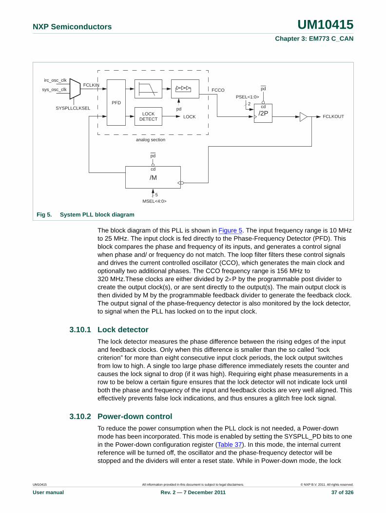
The block diagram of this PLL is shown in Figure 5. The input frequency range is 10 MHz to 25 MHz. The input clock is fed directly to the Phase-Frequency Detector (PFD). This block compares the phase and frequency of its inputs, and generates a control signal when phase and/ or frequency do not match. The loop filter filters these control signals and drives the current controlled oscillator (CCO), which generates the main clock and optionally two additional phases. The CCO frequency range is 156 MHz to 320 MHz.These clocks are either divided by 2P by the programmable post divider to create the output clock(s), or are sent directly to the output(s). The main output clock is then divided by M by the programmable feedback divider to generate the feedback clock. The output signal of the phase-frequency detector is also monitored by the lock detector, to signal when the PLL has locked on to the input clock.
3.10.1 Lock detector
The lock detector measures the phase difference between the rising edges of the input and feedback clocks. Only when this difference is smaller than the so called “lock criterion” for more than eight consecutive input clock periods, the lock output switches from low to high. A single too large phase difference immediately resets the counter and causes the lock signal to drop (if it was high). Requiring eight phase measurements in a row to be below a certain figure ensures that the lock detector will not indicate lock until both the phase and frequency of the input and feedback clocks are very well aligned. This effectively prevents false lock indications, and thus ensures a glitch free lock signal.
3.10.2 Power-down control
To reduce the power consumption when the PLL clock is not needed, a Power-down mode has been incorporated. This mode is enabled by setting the SYSPLL_PD bits to one in the Power-down configuration register (Table 37). In this mode, the internal current reference will be turned off, the oscillator and the phase-frequency detector will be stopped and the dividers will enter a reset state. While in Power-down mode, the lock
Fig 5. System PLL block diagram
LOCKDETECT
PFD
FCLKOUT
pd
analog section
pd
cd
/M
/2Pcd
PSEL<1:0>
pd
2
MSEL<4:0>5
irc_osc_clk
sys_osc_clk
SYSPLLCLKSEL
FCLKINFCCO
LOCK
UM10415 All information provided in this document is subject to legal disclaimers. © NXP B.V. 2011. All rights reserved.
User manual Rev. 2 — 7 December 2011 37 of 326

NXP Semiconductors UM10415Chapter 3: EM773 C_CAN
output will be low to indicate that the PLL is not in lock. When the Power-down mode is terminated by setting the SYSPLL_PD bits to zero, the PLL will resume its normal operation and will make the lock signal high once it has regained lock on the input clock.
3.10.3 Divider ratio programming
Post divider
The division ratio of the post divider is controlled by the PSEL bits. The division ratio is two times the value of P selected by PSEL bits as shown in Table 6. This guarantees an output clock with a 50% duty cycle.
Feedback divider
The feedback divider’s division ratio is controlled by the MSEL bits. The division ratio between the PLL’s output clock and the input clock is the decimal value on MSEL bits plus one, as specified in Table 6.
Changing the divider values
Changing the divider ratio while the PLL is running is not recommended. As there is no way to synchronize the change of the MSEL and PSEL values with the dividers, the risk exists that the counter will read in an undefined value, which could lead to unwanted spikes or drops in the frequency of the output clock. The recommended way of changing between divider settings is to power down the PLL, adjust the divider settings and then let the PLL start up again.
3.10.4 Frequency selection
The PLL frequency equations use the following parameters (also see Figure 3):
3.10.4.1 Normal mode
In normal mode the post divider is enabled, giving a 50% duty cycle clock with the following frequency relations:
(1)
To select the appropriate values for M and P, it is recommended to follow these steps:
1. Specify the input clock frequency Fclkin.
Table 39. PLL frequency parameters
Parameter System PLL
FCLKIN Frequency of sys_pllclkin (input clock to the system PLL) from the SYSPLLCLKSEL multiplexer (see Section 3.4.9).
FCCO Frequency of the Current Controlled Oscillator (CCO); 156 to 320 MHz.
FCLKOUT Frequency of sys_pllclkout
P System PLL post divider ratio; PSEL bits in SYSPLLCTRL (see Section 3.4.3).
M System PLL feedback divider register; MSEL bits in SYSPLLCTRL (see Section 3.4.3).
Fclkout M Fclkin FCCO 2 P = =
UM10415 All information provided in this document is subject to legal disclaimers. © NXP B.V. 2011. All rights reserved.
User manual Rev. 2 — 7 December 2011 38 of 326

NXP Semiconductors UM10415Chapter 3: EM773 C_CAN
2. Calculate M to obtain the desired output frequency Fclkout with M = Fclkout / Fclkin.
3. Find a value so that FCCO = 2 P Fclkout.
4. Verify that all frequencies and divider values conform to the limits specified in Table 6.
Table 40 shows how to configure the PLL for a 12 MHz crystal oscillator using the SYSPLLCTRL register (Table 6). The main clock is equivalent to the system clock if the system clock divider SYSAHBCLKDIV is set to one (see Table 16).
3.10.4.2 Power-down mode
In this mode, the internal current reference will be turned off, the oscillator and the phase-frequency detector will be stopped and the dividers will enter a reset state. While in Power-down mode, the lock output will be low, to indicate that the PLL is not in lock. When the Power-down mode is terminated by setting the SYSPLL_PD bit to zero in the Power-down configuration register (Table 37), the PLL will resume its normal operation and will make the lock signal HIGH once it has regained lock on the input clock.
3.11 Flash memory access
Depending on the system clock frequency, access to the flash memory can be configured with various access times by writing to the FLASHCFG register at address 0x4003 C010. This register is part of the flash configuration block (see Figure 2).
Remark: Improper setting of this register may result in incorrect operation of the EM773 flash memory.
Table 40. PLL configuration examples
PLL input clock sys_pllclkin (Fclkin)
Main clock (Fclkout)
MSEL bitsTable 6
M divider value
PSEL bitsTable 6
P divider value
FCCO frequency
12 MHz 48 MHz 00011 4 01 2 192 MHz
12 MHz 36 MHz 00010 3 10 4 288 MHz
12 MHz 24 MHz 00001 2 10 4 192 MHz
Table 41. Flash configuration register (FLASHCFG, address 0x4003 C010) bit description
Bit Symbol Value Description Reset value
1:0 FLASHTIM Flash memory access time. FLASHTIM +1 is equal to the number of system clocks used for flash access.
10
00 1 system clock flash access time (for system clock frequencies of up to 20 MHz).
01 2 system clocks flash access time (for system clock frequencies of up to 40 MHz).
10 3 system clocks flash access time (for system clock frequencies of up to 48 MHz).
11 Reserved.
31:2 - - Reserved. User software must not change the value of these bits. Bits 31:2 must be written back exactly as read.
<tbd>
UM10415 All information provided in this document is subject to legal disclaimers. © NXP B.V. 2011. All rights reserved.
User manual Rev. 2 — 7 December 2011 39 of 326

4.1 Introduction
The PMU controls the Deep power-down mode. Four general purpose register in the PMU can be used to retain data during Deep power-down mode.
4.2 Register description
4.2.1 Power control register
The power control register selects whether one of the ARM Cortex-M0 controlled power-down modes (Sleep mode or Deep-sleep mode) or the Deep power-down mode is entered and provides the flags for Sleep or Deep-sleep modes and Deep power-down modes respectively. See Section 3.8 for details on how to enter the power-down modes.
UM10415Chapter 4: EM773 PMU (Power Management Unit)Rev. 2 — 7 December 2011 User manual
Table 42. Register overview: PMU (base address 0x4003 8000)
Name Access Address offset
Description Reset value
PCON R/W 0x000 Power control register 0x0
GPREG0 R/W 0x004 General purpose register 0 0x0
GPREG1 R/W 0x008 General purpose register 1 0x0
GPREG2 R/W 0x00C General purpose register 2 0x0
GPREG3 R/W 0x010 General purpose register 3 0x0
GPREG4 R/W 0x014 General purpose register 4 0x0
Table 43. Power control register (PCON, address 0x4003 8000) bit description
Bit Symbol Value Description Reset value
0 - - Reserved. Do not write 1 to this bit. 0x0
1 DPDEN Deep power-down mode enable 0
0 ARM WFI will enter Sleep or Deep-sleep mode (clock to ARM Cortex-M0 core turned off).
1 ARM WFI will enter Deep-power down mode (ARM Cortex-M0 core powered-down).
7:2 - - Reserved. Do not write ones to this bit. 0x0
8 SLEEPFLAG Sleep mode flag 0
0 Read: No power-down mode entered. EM773 is in Active mode.Write: No effect.
1 Read: Sleep/Deep-sleep or Deep power-down mode entered.Write: Writing a 1 clears the SLEEPFLAG bit to 0.
10:9 - - Reserved. Do not write ones to this bit. 0x0
UM10415 All information provided in this document is subject to legal disclaimers. © NXP B.V. 2011. All rights reserved.
User manual Rev. 2 — 7 December 2011 40 of 326
NXP Semiconductors UM10415Chapter 4: EM773 PMU (Power Management Unit)
4.2.2 General purpose registers 0 to 3
The general purpose registers retain data through the Deep power-down mode when power is still applied to the VDD pin but the chip has entered Deep power-down mode. Only a “cold” boot when all power has been completely removed from the chip will reset the general purpose registers.
4.2.3 General purpose register 4
The general purpose register 4 retains data through the Deep power-down mode when power is still applied to the VDD pin but the chip has entered Deep power-down mode. Only a “cold” boot, when all power has been completely removed from the chip, will reset the general purpose registers.
Remark: If there is a possibility that the external voltage applied on pin VDD drops below 2.2 V during Deep power-down, the hysteresis of the WAKEUP input pin has to be disabled in this register before entering Deep power-down mode in order for the chip to wake up.
4.3 Functional description
For details of entering and exiting Deep power-down mode, see Section 3.8.
11 DPDFLAG Deep power-down flag 0x0
0 Read: Deep power-down mode not entered.Write: No effect.
0x0
1 Read: Deep power-down mode entered.Write: Clear the Deep power-down flag.
0x0
31:12 - - Reserved. Do not write ones to this bit. 0x0
Table 43. Power control register (PCON, address 0x4003 8000) bit description …continued
Bit Symbol Value Description Reset value
Table 44. General purpose registers 0 to 3 (GPREG0 - GPREG3, address 0x4003 8004 to 0x4003 8010) bit description
Bit Symbol Description Reset value
31:0 GPDATA Data retained during Deep power-down mode. 0x0
Table 45. General purpose register 4 (GPREG4, address 0x4003 8014) bit description
Bit Symbol Value Description Reset value
9:0 - - Reserved. Do not write ones to this bit. 0x0
10 WAKEUPHYS WAKEUP pin hysteresis enable 0x0
1 Hysteresis for WAKEUP pin enabled.
0 Hysteresis for WAKUP pin disabled.
31:11 GPDATA Data retained during Deep power-down mode. 0x0
UM10415 All information provided in this document is subject to legal disclaimers. © NXP B.V. 2011. All rights reserved.
User manual Rev. 2 — 7 December 2011 41 of 326

5.1 Introduction
The Nested Vectored Interrupt Controller (NVIC) is an integral part of the Cortex-M0. The tight coupling to the CPU allows for low interrupt latency and efficient processing of late arriving interrupts.
5.2 Features
• Nested Vectored Interrupt Controller that is an integral part of the ARM Cortex-M0
• Tightly coupled interrupt controller provides low interrupt latency
• Controls system exceptions and peripheral interrupts
• The NVIC supports 32 vectored interrupts
• 4 programmable interrupt priority levels with hardware priority level masking
• Software interrupt generation
5.3 Interrupt sources
Table 46 lists the interrupt sources for each peripheral function. Each peripheral device may have one or more interrupt lines to the Vectored Interrupt Controller. Each line may represent more than one interrupt source. There is no significance or priority about what line is connected where, except for certain standards from ARM.
UM10415Chapter 5: EM773 Interrupt controllerRev. 2 — 7 December 2011 User manual
Table 46. Connection of interrupt sources to the Vectored Interrupt Controller
Exception Number
Vector Offset
Function Flag(s)
10 to 0 start logic wake-up interrupts
Each interrupt is connected to a PIO input pin serving as wake-up pin from Deep-sleep mode; Interrupt 0 to 10 correspond to PIO0_0 to PIO0_10; see Section 3.4.27.
14 to 11 - Reserved
15 I2C SI (state change)
16 CT16B0 Match 0 - 2
Capture 0
17 Metrology Engine Metrology Engine interrupt (Section 18.2.2)
18 CT32B0 Match 0 - 3
Capture 0
19 CT32B1 Match 0 - 3
Capture 0
20 SPI/SSP0 Tx FIFO half empty
Rx FIFO half full
Rx Timeout
Rx Overrun
UM10415 All information provided in this document is subject to legal disclaimers. © NXP B.V. 2011. All rights reserved.
User manual Rev. 2 — 7 December 2011 42 of 326
NXP Semiconductors UM10415Chapter 5: EM773 Interrupt controller
21 UART Rx Line Status (RLS)
Transmit Holding Register Empty (THRE)
Rx Data Available (RDA)
Character Time-out Indicator (CTI)
End of Auto-Baud (ABEO)
Auto-Baud Time-Out (ABTO)
22 - Reserved
23 - Reserved
24 - Reserved
25 WDT Watchdog interrupt (WDINT)
26 BOD Brown-out detect
27 - Reserved
28 PIO_3 GPIO interrupt status of port 3
29 PIO_2 GPIO interrupt status of port 2
30 PIO_1 GPIO interrupt status of port 1
31 PIO_0 GPIO interrupt status of port 0
Table 46. Connection of interrupt sources to the Vectored Interrupt Controller …continued
Exception Number
Vector Offset
Function Flag(s)
UM10415 All information provided in this document is subject to legal disclaimers. © NXP B.V. 2011. All rights reserved.
User manual Rev. 2 — 7 December 2011 43 of 326

6.1 How to read this chapter
The implementation of the I/O configuration registers varies for different EM773 parts and packages.
6.2 Introduction
The I/O configuration registers control the electrical characteristics of the pads. The following features are programmable:
• pin function
• internal pull-up/pull-down resistor or bus keeper function
• hysteresis
• I2C mode for pads hosting the I2C-bus function
6.3 General description
The IOCON registers control the function (GPIO or peripheral function), the input mode, and the hysteresis of all PIOn_m pins. In addition, the I2C-bus pins can be configured for different I2C-bus modes.
UM10415Chapter 6: EM773 I/O ConfigurationRev. 2 — 7 December 2011 User manual
Fig 6. Standard I/O pin configuration
PIN
VDD
ESD
VSS
ESD
VDD
weakpull-up
weakpull-down
output enable
repeater modeenable
output
pull-up enable
pull-down enable
data inputEM773_002aaf304
pin configuredas digital output
driver
pin configuredas digital input
UM10415 All information provided in this document is subject to legal disclaimers. © NXP B.V. 2011. All rights reserved.
User manual Rev. 2 — 7 December 2011 44 of 326
NXP Semiconductors UM10415Chapter 6: EM773 I/O Configuration
6.3.1 Pin function
The FUNC bits in the IOCON registers can be set to GPIO (FUNC = 000) or to a peripheral function. If the pins are GPIO pins, the GPIOnDIR registers determine whether the pin is configured as an input or output (see Section 8.3.2). For any peripheral function, the pin direction is controlled automatically depending on the pin’s functionality. The GPIOnDIR registers have no effect for peripheral functions.
6.3.2 Pin mode
The MODE bits in the IOCON register allow the selection of on-chip pull-up or pull-down resistors for each pin or select the repeater mode.
The possible on-chip resistor configurations are pull-up enabled, pull-down enabled, or no pull-up/pull-down. The default value is pull-up enabled.
The repeater mode enables the pull-up resistor if the pin is at a logic HIGH and enables the pull-down resistor if the pin is at a logic LOW. This causes the pin to retain its last known state if it is configured as an input and is not driven externally. The state retention is not applicable to the Deep power-down mode. Repeater mode may typically be used to prevent a pin from floating (and potentially using significant power if it floats to an indeterminate state) if it is temporarily not driven.
6.3.3 Hysteresis
The input buffer for digital functions can be configured with hysteresis or as plain buffer through the IOCON registers (see the EM773 data sheet for details).
If the external pad supply voltage VDD is between 2.5 V and 3.6 V, the hysteresis buffer can be enabled or disabled. If VDD is below 2.5 V, the hysteresis buffer must be disabled to use the pin in input mode.
6.3.4 I2C mode
If the I2C function is selected by the FUNC bits of registers IOCON_PIO0_4 (Table 55) and IOCON_PIO0_5 (Table 56), then the I2C-bus pins can be configured for different I2C-modes:
• Standard mode/Fast-mode I2C with input glitch filter (this includes an open-drain output according to the I2C-bus specification).
• Fast-mode Plus with input glitch filter (this includes an open-drain output according to the I2C-bus specification). In this mode, the pins function as high-current sinks.
• Standard open-drain I/O functionality without input filter.
Remark: Either Standard mode/Fast-mode I2C or Standard I/O functionality should be selected if the pin is used as GPIO pin.
6.3.5 Open-drain Mode
When output is selected, either by selecting a special function in the FUNC field, or by selecting GPIO function for a pin having a 1 in its GPIODIR register, a 1 in the OD bit selects open-drain operation, that is, a 1 disables the high-drive transistor. This option has no effect on the primary I2C pins.
UM10415 All information provided in this document is subject to legal disclaimers. © NXP B.V. 2011. All rights reserved.
User manual Rev. 2 — 7 December 2011 45 of 326
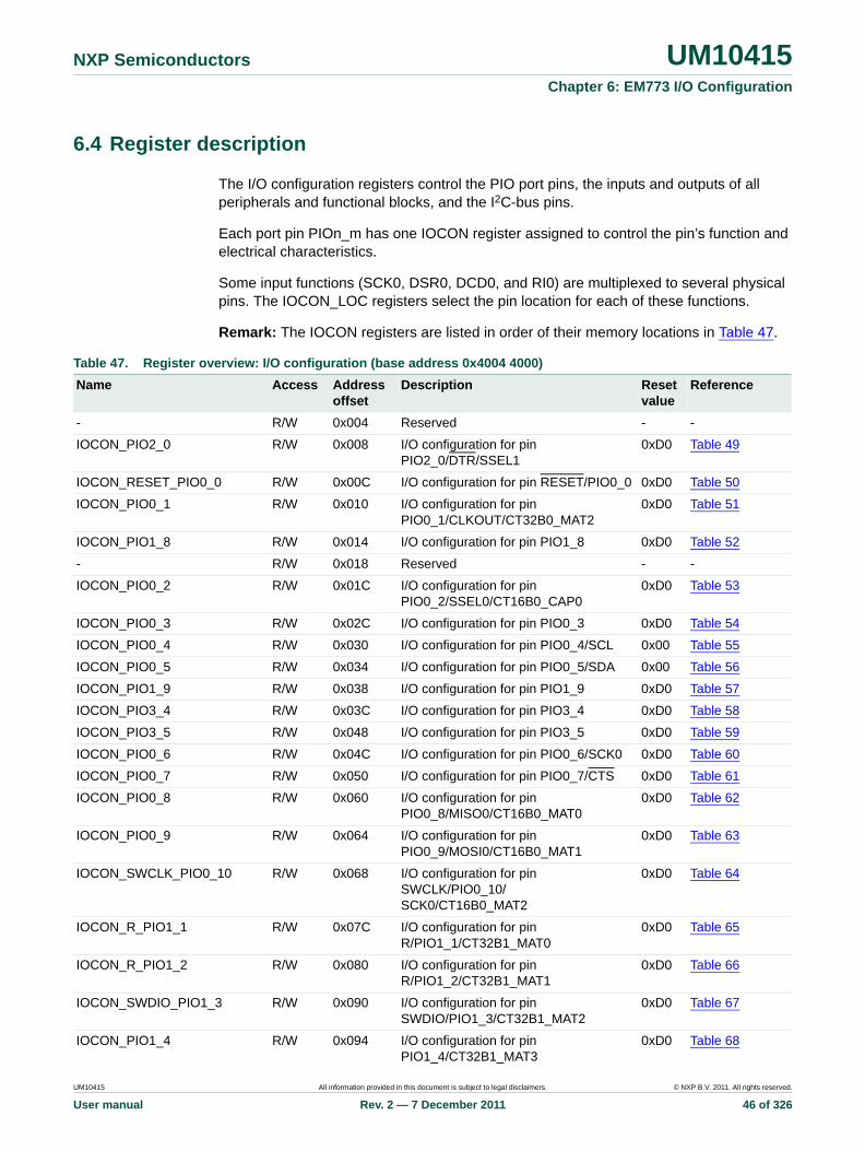
NXP Semiconductors UM10415Chapter 6: EM773 I/O Configuration
6.4 Register description
The I/O configuration registers control the PIO port pins, the inputs and outputs of all peripherals and functional blocks, and the I2C-bus pins.
Each port pin PIOn_m has one IOCON register assigned to control the pin’s function and electrical characteristics.
Some input functions (SCK0, DSR0, DCD0, and RI0) are multiplexed to several physical pins. The IOCON_LOC registers select the pin location for each of these functions.
Remark: The IOCON registers are listed in order of their memory locations in Table 47.
Table 47. Register overview: I/O configuration (base address 0x4004 4000)
Name Access Address offset
Description Reset value
Reference
- R/W 0x004 Reserved - -
IOCON_PIO2_0 R/W 0x008 I/O configuration for pin PIO2_0/DTR/SSEL1
0xD0 Table 49
IOCON_RESET_PIO0_0 R/W 0x00C I/O configuration for pin RESET/PIO0_0 0xD0 Table 50
IOCON_PIO0_1 R/W 0x010 I/O configuration for pin PIO0_1/CLKOUT/CT32B0_MAT2
0xD0 Table 51
IOCON_PIO1_8 R/W 0x014 I/O configuration for pin PIO1_8 0xD0 Table 52
- R/W 0x018 Reserved - -
IOCON_PIO0_2 R/W 0x01C I/O configuration for pin PIO0_2/SSEL0/CT16B0_CAP0
0xD0 Table 53
IOCON_PIO0_3 R/W 0x02C I/O configuration for pin PIO0_3 0xD0 Table 54
IOCON_PIO0_4 R/W 0x030 I/O configuration for pin PIO0_4/SCL 0x00 Table 55
IOCON_PIO0_5 R/W 0x034 I/O configuration for pin PIO0_5/SDA 0x00 Table 56
IOCON_PIO1_9 R/W 0x038 I/O configuration for pin PIO1_9 0xD0 Table 57
IOCON_PIO3_4 R/W 0x03C I/O configuration for pin PIO3_4 0xD0 Table 58
IOCON_PIO3_5 R/W 0x048 I/O configuration for pin PIO3_5 0xD0 Table 59
IOCON_PIO0_6 R/W 0x04C I/O configuration for pin PIO0_6/SCK0 0xD0 Table 60
IOCON_PIO0_7 R/W 0x050 I/O configuration for pin PIO0_7/CTS 0xD0 Table 61
IOCON_PIO0_8 R/W 0x060 I/O configuration for pin PIO0_8/MISO0/CT16B0_MAT0
0xD0 Table 62
IOCON_PIO0_9 R/W 0x064 I/O configuration for pin PIO0_9/MOSI0/CT16B0_MAT1
0xD0 Table 63
IOCON_SWCLK_PIO0_10 R/W 0x068 I/O configuration for pin SWCLK/PIO0_10/SCK0/CT16B0_MAT2
0xD0 Table 64
IOCON_R_PIO1_1 R/W 0x07C I/O configuration for pin R/PIO1_1/CT32B1_MAT0
0xD0 Table 65
IOCON_R_PIO1_2 R/W 0x080 I/O configuration for pin R/PIO1_2/CT32B1_MAT1
0xD0 Table 66
IOCON_SWDIO_PIO1_3 R/W 0x090 I/O configuration for pin SWDIO/PIO1_3/CT32B1_MAT2
0xD0 Table 67
IOCON_PIO1_4 R/W 0x094 I/O configuration for pin PIO1_4/CT32B1_MAT3
0xD0 Table 68
UM10415 All information provided in this document is subject to legal disclaimers. © NXP B.V. 2011. All rights reserved.
User manual Rev. 2 — 7 December 2011 46 of 326

NXP Semiconductors UM10415Chapter 6: EM773 I/O Configuration
IOCON_PIO1_11 R/W 0x098 I/O configuration for pin PIO1_11 0xD0 Table 69
IOCON_PIO3_2 R/W 0x09C I/O configuration for pin PIO3_2/DCD 0xD0 Table 70
IOCON_PIO1_5 R/W 0x0A0 I/O configuration for pin PIO1_5/RTS/CT32B0_CAP0
0xD0 Table 71
IOCON_PIO1_6 R/W 0x0A4 I/O configuration for pin PIO1_6/RXD/CT32B0_MAT0
0xD0 Table 72
IOCON_PIO1_7 R/W 0x0A8 I/O configuration for pin PIO1_7/TXD/CT32B0_MAT1
0xD0 Table 73
IOCON_SCK_LOC R/W 0x0B0 SCK pin location select register 0x00 Table 74
Table 47. Register overview: I/O configuration (base address 0x4004 4000)
Name Access Address offset
Description Reset value
Reference
Table 48. I/O configuration registers ordered by port number
Port pin Register name Reference
PIO0_0 IOCON_RESET_PIO0_0 Table 50
PIO0_1 IOCON_PIO0_1 Table 51
PIO0_2 IOCON_PIO0_2 Table 53
PIO0_3 IOCON_PIO0_3 Table 54
PIO0_4 IOCON_PIO0_4 Table 55
PIO0_5 IOCON_PIO0_5 Table 56
PIO0_6 IOCON_PIO0_6 Table 60
PIO0_7 IOCON_PIO0_7 Table 61
PIO0_8 IOCON_PIO0_8 Table 62
PIO0_9 IOCON_PIO0_9 Table 63
PIO0_10 IOCON_SWCLK_PIO0_10 Table 64
PIO1_1 IOCON_R_PIO1_1 Table 65
PIO1_2 IOCON_R_PIO1_2 Table 66
PIO1_3 IOCON_SWDIO_PIO1_3 Table 67
PIO1_4 IOCON_PIO1_4 Table 68
PIO1_5 IOCON_PIO1_5 Table 71
PIO1_6 IOCON_PIO1_6 Table 72
PIO1_7 IOCON_PIO1_7 Table 73
PIO1_8 IOCON_PIO1_8 Table 52
PIO1_9 IOCON_PIO1_9 Table 57
PIO1_11 IOCON_PIO1_11 Table 69
PIO2_0 IOCON_PIO2_0 Table 49
PIO3_2 IOCON_PIO3_2 Table 70
PIO3_4 IOCON_PIO3_4 Table 58
PIO3_5 IOCON_PIO3_5 Table 59
- IOCON_SCK_LOC Table 74
UM10415 All information provided in this document is subject to legal disclaimers. © NXP B.V. 2011. All rights reserved.
User manual Rev. 2 — 7 December 2011 47 of 326

NXP Semiconductors UM10415Chapter 6: EM773 I/O Configuration
6.4.1 I/O configuration registers IOCON_PIOn
For details on the I/O configuration settings, see Section 6.3.
Table 49. IOCON_PIO2_0 register (IOCON_PIO2_0, address 0x4004 4008) bit description
Bit Symbol Value Description Reset value
2:0 FUNC Selects pin function. 000
000 Selects function PIO2_0.
001 Select function DTR.
010 Select function SSEL1.
011 to
111
Reserved.
4:3 MODE Selects function mode (on-chip pull-up/pull-down resistor control).
10
00 Inactive (no pull-down/pull-up resistor enabled).
01 Pull-down resistor enabled.
10 Pull-up resistor enabled.
11 Repeater mode.
5 HYS Hysteresis. 0
0 Disable.
1 Enable.
9:6 - - Reserved 0011
10 OD Selects pseudo open-drain mode. 0
0 Standard GPIO output
1 Open-drain output
31:11 - - Reserved -
Table 50. IOCON_nRESET_PIO0_0 register (IOCON_nRESET_PIO0_0, address 0x4004 400C) bit description
Bit Symbol Value Description Reset value
2:0 FUNC Selects pin function. 000
000 Selects function RESET.
001 Selects function PIO0_0.
010 to
111
Reserved.
4:3 MODE Selects function mode (on-chip pull-up/pull-down resistor control).
10
00 Inactive (no pull-down/pull-up resistor enabled).
01 Pull-down resistor enabled.
10 Pull-up resistor enabled.
11 Repeater mode.
5 HYS Hysteresis. 0
0 Disable.
1 Enable.
UM10415 All information provided in this document is subject to legal disclaimers. © NXP B.V. 2011. All rights reserved.
User manual Rev. 2 — 7 December 2011 48 of 326

NXP Semiconductors UM10415Chapter 6: EM773 I/O Configuration
9:6 - - Reserved 0011
10 OD Selects pseudo open-drain mode. 0
0 Standard GPIO output
1 Open-drain output
31:11 - - Reserved -
Table 51. IOCON_PIO0_1 register (IOCON_PIO0_1, address 0x4004 4010) bit description
Bit Symbol Value Description Reset value
2:0 FUNC Selects pin function. 000
000 Selects function PIO0_1.
001 Selects function CLKOUT.
010 Selects function CT32B0_MAT2.
011 to
111
Reserved.
4:3 MODE Selects function mode (on-chip pull-up/pull-down resistor control).
10
00 Inactive (no pull-down/pull-up resistor enabled).
01 Pull-down resistor enabled.
10 Pull-up resistor enabled.
11 Repeater mode.
5 HYS Hysteresis. 0
0 Disable.
1 Enable.
9:6 - - Reserved 0011
10 OD Selects pseudo open-drain mode. 0
0 Standard GPIO output
1 Open-drain output
31:11 - - Reserved -
Table 52. IOCON_PIO1_8 register (IOCON_PIO1_8, address 0x4004 4014) bit description
Bit Symbol Value Description Reset value
2:0 FUNC Selects pin function. 000
000 Selects function PIO1_8.
010 to
111
Reserved.
Table 50. IOCON_nRESET_PIO0_0 register (IOCON_nRESET_PIO0_0, address 0x4004 400C) bit description
Bit Symbol Value Description Reset value
UM10415 All information provided in this document is subject to legal disclaimers. © NXP B.V. 2011. All rights reserved.
User manual Rev. 2 — 7 December 2011 49 of 326
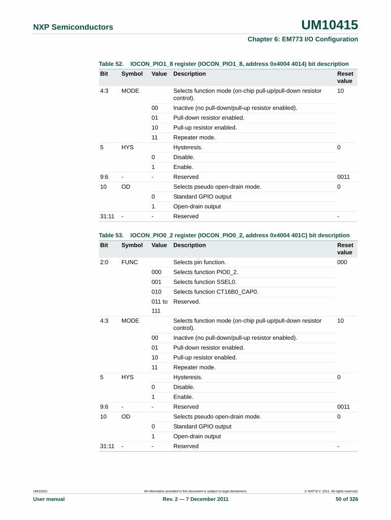
NXP Semiconductors UM10415Chapter 6: EM773 I/O Configuration
4:3 MODE Selects function mode (on-chip pull-up/pull-down resistor control).
10
00 Inactive (no pull-down/pull-up resistor enabled).
01 Pull-down resistor enabled.
10 Pull-up resistor enabled.
11 Repeater mode.
5 HYS Hysteresis. 0
0 Disable.
1 Enable.
9:6 - - Reserved 0011
10 OD Selects pseudo open-drain mode. 0
0 Standard GPIO output
1 Open-drain output
31:11 - - Reserved -
Table 53. IOCON_PIO0_2 register (IOCON_PIO0_2, address 0x4004 401C) bit description
Bit Symbol Value Description Reset value
2:0 FUNC Selects pin function. 000
000 Selects function PIO0_2.
001 Selects function SSEL0.
010 Selects function CT16B0_CAP0.
011 to
111
Reserved.
4:3 MODE Selects function mode (on-chip pull-up/pull-down resistor control).
10
00 Inactive (no pull-down/pull-up resistor enabled).
01 Pull-down resistor enabled.
10 Pull-up resistor enabled.
11 Repeater mode.
5 HYS Hysteresis. 0
0 Disable.
1 Enable.
9:6 - - Reserved 0011
10 OD Selects pseudo open-drain mode. 0
0 Standard GPIO output
1 Open-drain output
31:11 - - Reserved -
Table 52. IOCON_PIO1_8 register (IOCON_PIO1_8, address 0x4004 4014) bit description
Bit Symbol Value Description Reset value
UM10415 All information provided in this document is subject to legal disclaimers. © NXP B.V. 2011. All rights reserved.
User manual Rev. 2 — 7 December 2011 50 of 326

NXP Semiconductors UM10415Chapter 6: EM773 I/O Configuration
[1] Select Standard mode (I2CMODE = 00, default) or Standard I/O functionality (I2CMODE = 01) if the pin function is GPIO (FUNC = 000).
Table 54. IOCON_PIO0_3 register (IOCON_PIO0_3 address 0x4004 402C) bit description
Bit Symbol Value Description Reset value
2:0 FUNC Selects pin function. 000
000 Selects function PIO0_3.
001 to
111
Reserved.
4:3 MODE Selects function mode (on-chip pull-up/pull-down resistor control).
10
00 Inactive (no pull-down/pull-up resistor enabled).
01 Pull-down resistor enabled.
10 Pull-up resistor enabled.
11 Repeater mode.
5 HYS Hysteresis. 0
0 Disable.
1 Enable.
9:6 - - Reserved 0011
10 OD Selects pseudo open-drain mode. 0
0 Standard GPIO output
1 Open-drain output
31:11 - - Reserved -
Table 55. IOCON_PIO0_4 register (IOCON_PIO0_4 address 0x4004 4030) bit description
Bit Symbol Value Description Reset value
2:0 FUNC Selects pin function. 000
000 Selects function PIO0_4 (open-drain pin).
001 Selects I2C function SCL (open-drain pin).
010 to
111
Reserved.
7:3 - Reserved. 00000
9:8 I2CMODE Selects I2C mode (see Section 6.3.4). 00
00[1] Standard mode/ Fast-mode I2C.
01[1] Standard I/O functionality
10 Fast-mode Plus I2C
11 Reserved.
31:10 - - Reserved. -
UM10415 All information provided in this document is subject to legal disclaimers. © NXP B.V. 2011. All rights reserved.
User manual Rev. 2 — 7 December 2011 51 of 326
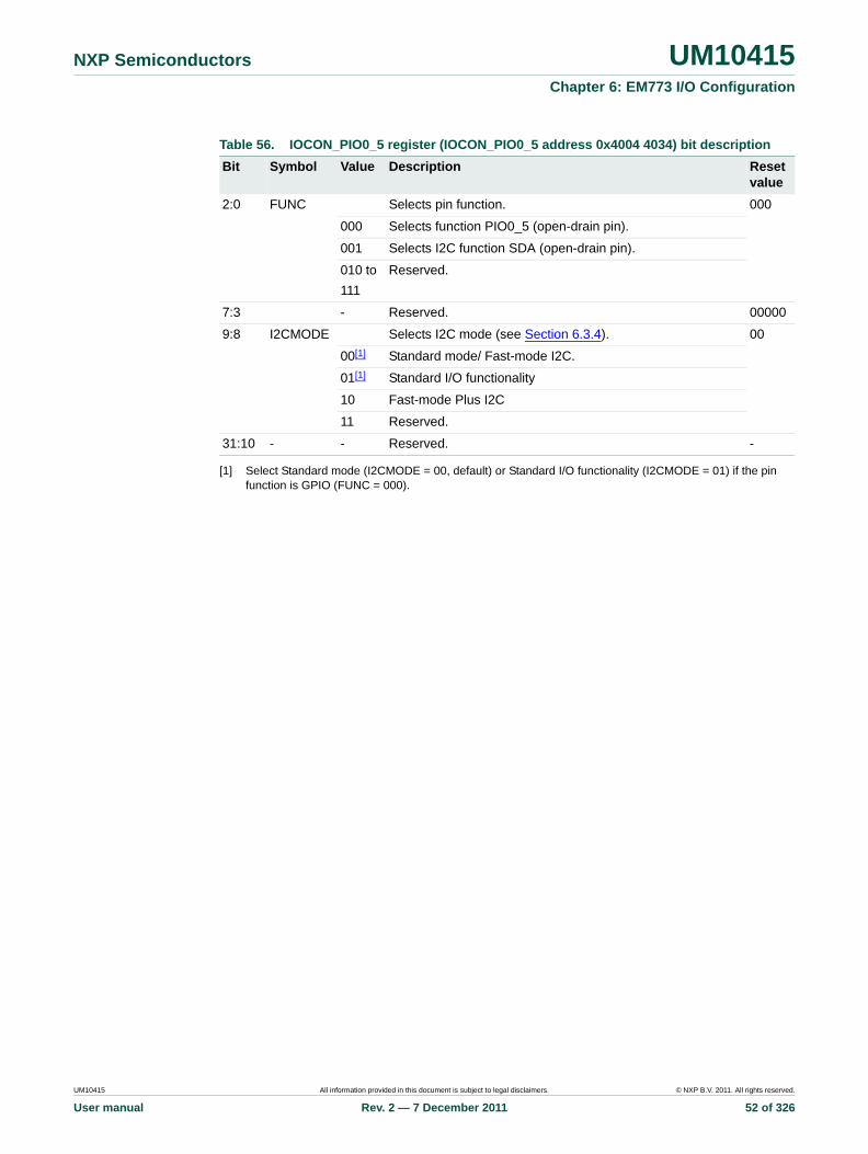
NXP Semiconductors UM10415Chapter 6: EM773 I/O Configuration
[1] Select Standard mode (I2CMODE = 00, default) or Standard I/O functionality (I2CMODE = 01) if the pin function is GPIO (FUNC = 000).
Table 56. IOCON_PIO0_5 register (IOCON_PIO0_5 address 0x4004 4034) bit description
Bit Symbol Value Description Reset value
2:0 FUNC Selects pin function. 000
000 Selects function PIO0_5 (open-drain pin).
001 Selects I2C function SDA (open-drain pin).
010 to
111
Reserved.
7:3 - Reserved. 00000
9:8 I2CMODE Selects I2C mode (see Section 6.3.4). 00
00[1] Standard mode/ Fast-mode I2C.
01[1] Standard I/O functionality
10 Fast-mode Plus I2C
11 Reserved.
31:10 - - Reserved. -
UM10415 All information provided in this document is subject to legal disclaimers. © NXP B.V. 2011. All rights reserved.
User manual Rev. 2 — 7 December 2011 52 of 326

NXP Semiconductors UM10415Chapter 6: EM773 I/O Configuration
Table 57. IOCON_PIO1_9 register (IOCON_PIO1_9 address 0x4004 4038) bit description
Bit Symbol Value Description Reset value
2:0 FUNC Selects pin function. 000
000 Selects function PIO1_9.
010 to
111
Reserved.
4:3 MODE Selects function mode (on-chip pull-up/pull-down resistor control).
10
00 Inactive (no pull-down/pull-up resistor enabled).
01 Pull-down resistor enabled.
10 Pull-up resistor enabled.
11 Repeater mode.
5 HYS Hysteresis. 0
0 Disable.
1 Enable.
9:6 - - Reserved 0011
10 OD Selects pseudo open-drain mode. 0
0 Standard GPIO output
1 Open-drain output
31:11 - - Reserved -
Table 58. IOCON_PIO3_4 register (IOCON_PIO3_4, address 0x4004 403C) bit description
Bit Symbol Value Description Reset value
2:0 FUNC Selects pin function. 000
000 Selects function PIO3_4.
001 to
111
Reserved.
4:3 MODE Selects function mode (on-chip pull-up/pull-down resistor control).
10
00 Inactive (no pull-down/pull-up resistor enabled).
01 Pull-down resistor enabled.
10 Pull-up resistor enabled.
11 Repeater mode.
5 HYS Hysteresis. 0
0 Disable.
1 Enable.
9:6 - - Reserved 0011
10 OD Selects pseudo open-drain mode. 0
0 Standard GPIO output
1 Open-drain output
31:11 - - Reserved -
UM10415 All information provided in this document is subject to legal disclaimers. © NXP B.V. 2011. All rights reserved.
User manual Rev. 2 — 7 December 2011 53 of 326

NXP Semiconductors UM10415Chapter 6: EM773 I/O Configuration
Table 59. IOCON_PIO3_5 register (IOCON_PIO3_5, address 0x4004 4048) bit description
Bit Symbol Value Description Reset value
2:0 FUNC Selects pin function. 000
000 Selects function PIO3_5.
001 to
111
Reserved.
4:3 MODE Selects function mode (on-chip pull-up/pull-down resistor control).
10
00 Inactive (no pull-down/pull-up resistor enabled).
01 Pull-down resistor enabled.
10 Pull-up resistor enabled.
11 Repeater mode.
5 HYS Hysteresis. 0
0 Disable.
1 Enable.
9:6 - - Reserved 0011
10 OD Selects pseudo open-drain mode. 0
0 Standard GPIO output
1 Open-drain output
31:11 - - Reserved -
Table 60. IOCON_PIO0_6 register (IOCON_PIO0_6 address 0x4004 404C) bit description
Bit Symbol Value Description Reset value
2:0 FUNC Selects pin function. 000
000 Selects function PIO0_6.
001 Reserved.
010 Selects function SCK0 (only if pin PIO0_6/SCK0 selected in Table 74).
011 to
111
Reserved.
4:3 MODE Selects function mode (on-chip pull-up/pull-down resistor control).
10
00 Inactive (no pull-down/pull-up resistor enabled).
01 Pull-down resistor enabled.
10 Pull-up resistor enabled.
11 Repeater mode.
5 HYS Hysteresis. 0
0 Disable.
1 Enable.
9:6 - - Reserved 0011
UM10415 All information provided in this document is subject to legal disclaimers. © NXP B.V. 2011. All rights reserved.
User manual Rev. 2 — 7 December 2011 54 of 326
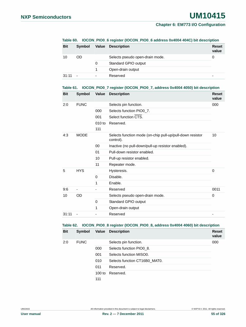
NXP Semiconductors UM10415Chapter 6: EM773 I/O Configuration
10 OD Selects pseudo open-drain mode. 0
0 Standard GPIO output
1 Open-drain output
31:11 - - Reserved -
Table 61. IOCON_PIO0_7 register (IOCON_PIO0_7, address 0x4004 4050) bit description
Bit Symbol Value Description Reset value
2:0 FUNC Selects pin function. 000
000 Selects function PIO0_7.
001 Select function CTS.
010 to
111
Reserved.
4:3 MODE Selects function mode (on-chip pull-up/pull-down resistor control).
10
00 Inactive (no pull-down/pull-up resistor enabled).
01 Pull-down resistor enabled.
10 Pull-up resistor enabled.
11 Repeater mode.
5 HYS Hysteresis. 0
0 Disable.
1 Enable.
9:6 - - Reserved 0011
10 OD Selects pseudo open-drain mode. 0
0 Standard GPIO output
1 Open-drain output
31:11 - - Reserved -
Table 62. IOCON_PIO0_8 register (IOCON_PIO0_8, address 0x4004 4060) bit description
Bit Symbol Value Description Reset value
2:0 FUNC Selects pin function. 000
000 Selects function PIO0_8.
001 Selects function MISO0.
010 Selects function CT16B0_MAT0.
011 Reserved.
100 to
111
Reserved.
Table 60. IOCON_PIO0_6 register (IOCON_PIO0_6 address 0x4004 404C) bit description
Bit Symbol Value Description Reset value
UM10415 All information provided in this document is subject to legal disclaimers. © NXP B.V. 2011. All rights reserved.
User manual Rev. 2 — 7 December 2011 55 of 326

NXP Semiconductors UM10415Chapter 6: EM773 I/O Configuration
4:3 MODE Selects function mode (on-chip pull-up/pull-down resistor control).
10
00 Inactive (no pull-down/pull-up resistor enabled).
01 Pull-down resistor enabled.
10 Pull-up resistor enabled.
11 Repeater mode.
5 HYS Hysteresis. 0
0 Disable.
1 Enable.
9:6 - - Reserved 0011
10 OD Selects pseudo open-drain mode. 0
0 Standard GPIO output
1 Open-drain output
31:11 - - Reserved -
Table 63. IOCON_PIO0_9 register (IOCON_PIO0_9, address 0x4004 4064) bit description
Bit Symbol Value Description Reset value
2:0 FUNC Selects pin function. 000
000 Selects function PIO0_9.
001 Selects function MOSI0.
010 Selects function CT16B0_MAT1.
011 to
111
Reserved.
4:3 MODE Selects function mode (on-chip pull-up/pull-down resistor control).
10
00 Inactive (no pull-down/pull-up resistor enabled).
01 Pull-down resistor enabled.
10 Pull-up resistor enabled.
11 Repeater mode.
5 HYS Hysteresis. 0
0 Disable.
1 Enable.
9:6 - - Reserved 0011
10 OD Selects pseudo open-drain mode. 0
0 Standard GPIO output
1 Open-drain output
31:11 - - Reserved -
Table 62. IOCON_PIO0_8 register (IOCON_PIO0_8, address 0x4004 4060) bit description
Bit Symbol Value Description Reset value
UM10415 All information provided in this document is subject to legal disclaimers. © NXP B.V. 2011. All rights reserved.
User manual Rev. 2 — 7 December 2011 56 of 326

NXP Semiconductors UM10415Chapter 6: EM773 I/O Configuration
Table 64. IOCON_SWCLK_PIO0_10 register (IOCON_SWCLK_PIO0_10, address 0x4004 4068) bit description
Bit Symbol Value Description Reset value
2:0 FUNC Selects pin function. 000
000 Selects function SWCLK.
001 Selects function PIO0_10.
010 Selects function SCK0 (only if pin SWCLK/PIO0_10/SCK0/CT16B0_MAT2 selected in Table 74).
011 Selects function CT16B0_MAT2.
100 to
111
Reserved.
4:3 MODE Selects function mode (on-chip pull-up/pull-down resistor control).
10
00 Inactive (no pull-down/pull-up resistor enabled).
01 Pull-down resistor enabled.
10 Pull-up resistor enabled.
11 Repeater mode.
5 HYS Hysteresis. 0
0 Disable.
1 Enable.
9:6 - - Reserved 0011
10 OD Selects pseudo open-drain mode. 0
0 Standard GPIO output
1 Open-drain output
31:11 - - Reserved -
UM10415 All information provided in this document is subject to legal disclaimers. © NXP B.V. 2011. All rights reserved.
User manual Rev. 2 — 7 December 2011 57 of 326

NXP Semiconductors UM10415Chapter 6: EM773 I/O Configuration
Table 65. IOCON_R_PIO1_1 register (IOCON_R_PIO1_1, address 0x4004 407C) bit description
Bit Symbol Value Description Reset value
2:0 FUNC Selects pin function. 000
000 Selects function R. This function is reserved. Select one of the alternate functions below.
001 Selects function PIO1_1.
011 Selects function CT32B1_MAT0.
100 to
111
Reserved.
4:3 MODE Selects function mode (on-chip pull-up/pull-down resistor control).
10
00 Inactive (no pull-down/pull-up resistor enabled).
01 Pull-down resistor enabled.
10 Pull-up resistor enabled.
11 Repeater mode.
5 HYS Hysteresis. 0
0 Disable.
1 Enable.
UM10415 All information provided in this document is subject to legal disclaimers. © NXP B.V. 2011. All rights reserved.
User manual Rev. 2 — 7 December 2011 58 of 326
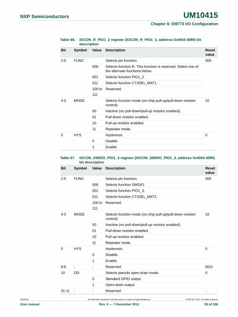
NXP Semiconductors UM10415Chapter 6: EM773 I/O Configuration
Table 66. IOCON_R_PIO1_2 register (IOCON_R_PIO1_2, address 0x4004 4080) bit description
Bit Symbol Value Description Reset value
2:0 FUNC Selects pin function. 000
000 Selects function R. This function is reserved. Select one of the alternate functions below.
001 Selects function PIO1_2.
011 Selects function CT32B1_MAT1.
100 to
111
Reserved.
4:3 MODE Selects function mode (on-chip pull-up/pull-down resistor control).
10
00 Inactive (no pull-down/pull-up resistor enabled).
01 Pull-down resistor enabled.
10 Pull-up resistor enabled.
11 Repeater mode.
5 HYS Hysteresis. 0
0 Disable.
1 Enable.
Table 67. IOCON_SWDIO_PIO1_3 register (IOCON_SWDIO_PIO1_3, address 0x4004 4090) bit description
Bit Symbol Value Description Reset value
2:0 FUNC Selects pin function. 000
000 Selects function SWDIO.
001 Selects function PIO1_3.
011 Selects function CT32B1_MAT2.
100 to
111
Reserved.
4:3 MODE Selects function mode (on-chip pull-up/pull-down resistor control).
10
00 Inactive (no pull-down/pull-up resistor enabled).
01 Pull-down resistor enabled.
10 Pull-up resistor enabled.
11 Repeater mode.
5 HYS Hysteresis. 0
0 Disable.
1 Enable.
9:6 - - Reserved 0011
10 OD Selects pseudo open-drain mode. 0
0 Standard GPIO output
1 Open-drain output
31:11 - - Reserved -
UM10415 All information provided in this document is subject to legal disclaimers. © NXP B.V. 2011. All rights reserved.
User manual Rev. 2 — 7 December 2011 59 of 326
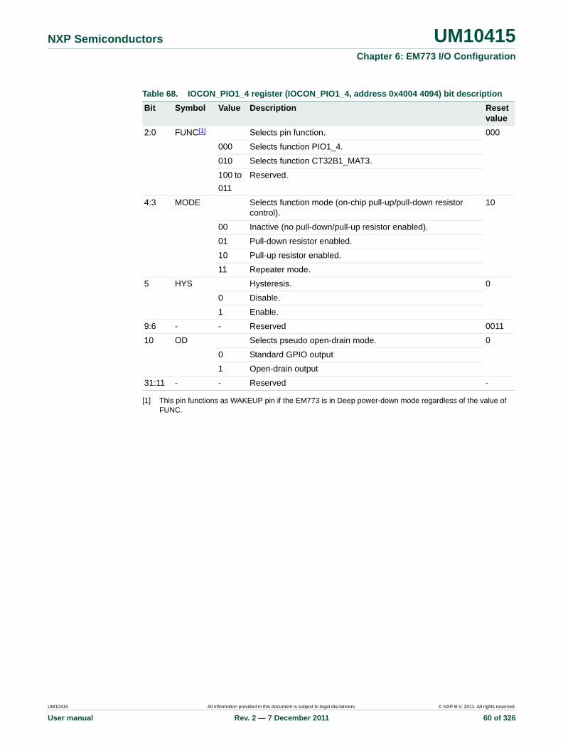
NXP Semiconductors UM10415Chapter 6: EM773 I/O Configuration
[1] This pin functions as WAKEUP pin if the EM773 is in Deep power-down mode regardless of the value of FUNC.
Table 68. IOCON_PIO1_4 register (IOCON_PIO1_4, address 0x4004 4094) bit description
Bit Symbol Value Description Reset value
2:0 FUNC[1] Selects pin function. 000
000 Selects function PIO1_4.
010 Selects function CT32B1_MAT3.
100 to
011
Reserved.
4:3 MODE Selects function mode (on-chip pull-up/pull-down resistor control).
10
00 Inactive (no pull-down/pull-up resistor enabled).
01 Pull-down resistor enabled.
10 Pull-up resistor enabled.
11 Repeater mode.
5 HYS Hysteresis. 0
0 Disable.
1 Enable.
9:6 - - Reserved 0011
10 OD Selects pseudo open-drain mode. 0
0 Standard GPIO output
1 Open-drain output
31:11 - - Reserved -
UM10415 All information provided in this document is subject to legal disclaimers. © NXP B.V. 2011. All rights reserved.
User manual Rev. 2 — 7 December 2011 60 of 326
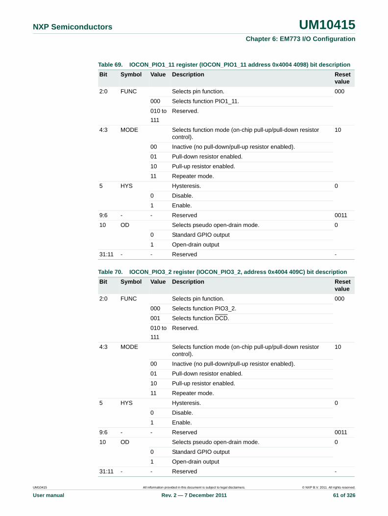
NXP Semiconductors UM10415Chapter 6: EM773 I/O Configuration
Table 69. IOCON_PIO1_11 register (IOCON_PIO1_11 address 0x4004 4098) bit description
Bit Symbol Value Description Reset value
2:0 FUNC Selects pin function. 000
000 Selects function PIO1_11.
010 to
111
Reserved.
4:3 MODE Selects function mode (on-chip pull-up/pull-down resistor control).
10
00 Inactive (no pull-down/pull-up resistor enabled).
01 Pull-down resistor enabled.
10 Pull-up resistor enabled.
11 Repeater mode.
5 HYS Hysteresis. 0
0 Disable.
1 Enable.
9:6 - - Reserved 0011
10 OD Selects pseudo open-drain mode. 0
0 Standard GPIO output
1 Open-drain output
31:11 - - Reserved -
Table 70. IOCON_PIO3_2 register (IOCON_PIO3_2, address 0x4004 409C) bit description
Bit Symbol Value Description Reset value
2:0 FUNC Selects pin function. 000
000 Selects function PIO3_2.
001 Selects function DCD.
010 to
111
Reserved.
4:3 MODE Selects function mode (on-chip pull-up/pull-down resistor control).
10
00 Inactive (no pull-down/pull-up resistor enabled).
01 Pull-down resistor enabled.
10 Pull-up resistor enabled.
11 Repeater mode.
5 HYS Hysteresis. 0
0 Disable.
1 Enable.
9:6 - - Reserved 0011
10 OD Selects pseudo open-drain mode. 0
0 Standard GPIO output
1 Open-drain output
31:11 - - Reserved -
UM10415 All information provided in this document is subject to legal disclaimers. © NXP B.V. 2011. All rights reserved.
User manual Rev. 2 — 7 December 2011 61 of 326

NXP Semiconductors UM10415Chapter 6: EM773 I/O Configuration
Table 71. IOCON_PIO1_5 register (IOCON_PIO1_5, address 0x4004 40A0) bit description
Bit Symbol Value Description Reset value
2:0 FUNC Selects pin function. 000
000 Selects function PIO1_5.
001 Selects function RTS.
010 Selects function CT32B0_CAP0.
011 to
111
Reserved.
4:3 MODE Selects function mode (on-chip pull-up/pull-down resistor control).
10
00 Inactive (no pull-down/pull-up resistor enabled).
01 Pull-down resistor enabled.
10 Pull-up resistor enabled.
11 Repeater mode.
5 HYS Hysteresis. 0
0 Disable.
1 Enable.
9:6 - - Reserved 0011
10 OD Selects pseudo open-drain mode. 0
0 Standard GPIO output
1 Open-drain output
31:11 - - Reserved -
Table 72. IOCON_PIO1_6 register (IOCON_PIO1_6, address 0x4004 40A4) bit description
Bit Symbol Value Description Reset value
2:0 FUNC Selects pin function. 000
000 Selects function PIO1_6.
001 Selects function RXD.
010 Selects function CT32B0_MAT0.
011 to
111
Reserved.
4:3 MODE Selects function mode (on-chip pull-up/pull-down resistor control).
10
00 Inactive (no pull-down/pull-up resistor enabled).
01 Pull-down resistor enabled.
10 Pull-up resistor enabled.
11 Repeater mode.
5 HYS Hysteresis. 0
0 Disable.
1 Enable.
9:6 - - Reserved 0011
UM10415 All information provided in this document is subject to legal disclaimers. © NXP B.V. 2011. All rights reserved.
User manual Rev. 2 — 7 December 2011 62 of 326
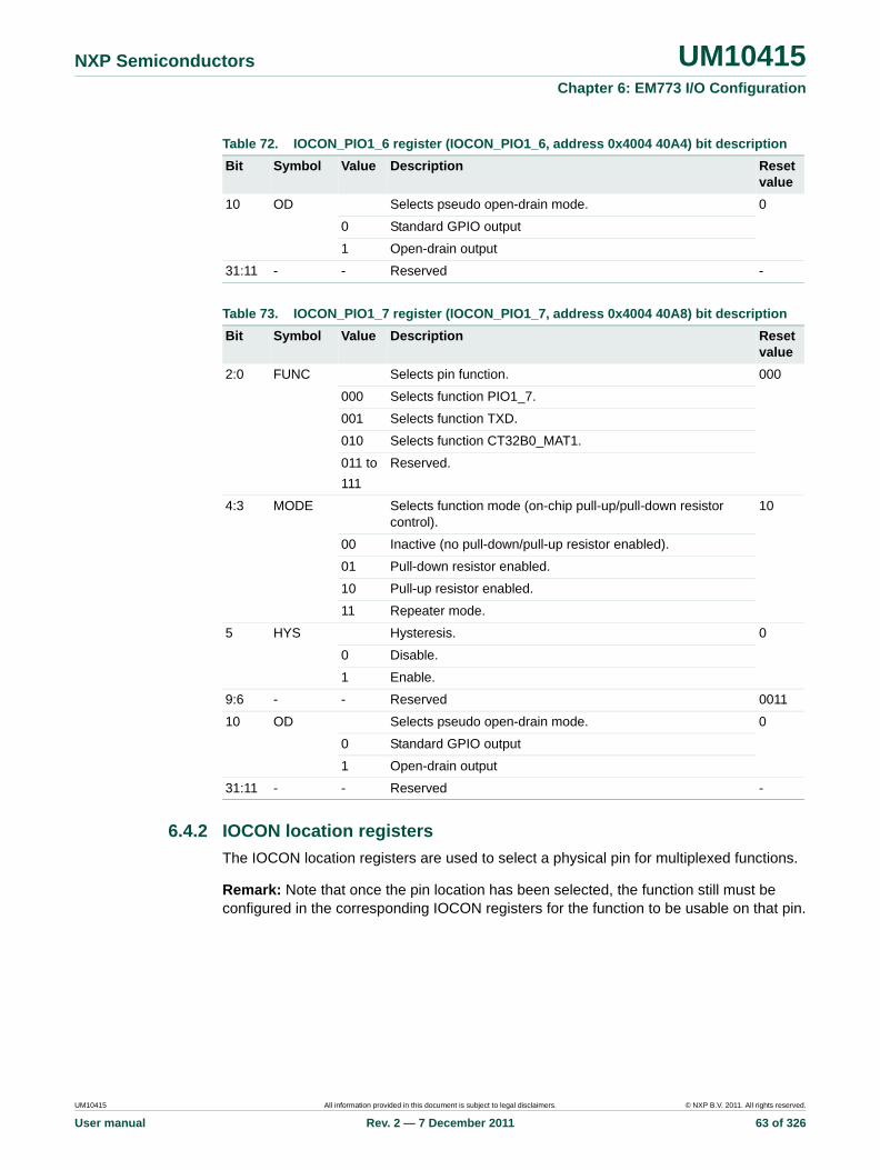
NXP Semiconductors UM10415Chapter 6: EM773 I/O Configuration
6.4.2 IOCON location registers
The IOCON location registers are used to select a physical pin for multiplexed functions.
Remark: Note that once the pin location has been selected, the function still must be configured in the corresponding IOCON registers for the function to be usable on that pin.
10 OD Selects pseudo open-drain mode. 0
0 Standard GPIO output
1 Open-drain output
31:11 - - Reserved -
Table 73. IOCON_PIO1_7 register (IOCON_PIO1_7, address 0x4004 40A8) bit description
Bit Symbol Value Description Reset value
2:0 FUNC Selects pin function. 000
000 Selects function PIO1_7.
001 Selects function TXD.
010 Selects function CT32B0_MAT1.
011 to
111
Reserved.
4:3 MODE Selects function mode (on-chip pull-up/pull-down resistor control).
10
00 Inactive (no pull-down/pull-up resistor enabled).
01 Pull-down resistor enabled.
10 Pull-up resistor enabled.
11 Repeater mode.
5 HYS Hysteresis. 0
0 Disable.
1 Enable.
9:6 - - Reserved 0011
10 OD Selects pseudo open-drain mode. 0
0 Standard GPIO output
1 Open-drain output
31:11 - - Reserved -
Table 72. IOCON_PIO1_6 register (IOCON_PIO1_6, address 0x4004 40A4) bit description
Bit Symbol Value Description Reset value
UM10415 All information provided in this document is subject to legal disclaimers. © NXP B.V. 2011. All rights reserved.
User manual Rev. 2 — 7 December 2011 63 of 326

NXP Semiconductors UM10415Chapter 6: EM773 I/O Configuration
Table 74. IOCON SCK location register (IOCON_SCK_LOC, address 0x4004 40B0) bit description
Bit Symbol Value Description Reset value
1:0 SCKLOC Selects pin location for SCK0 pin. 00
00 Selects SCK0 function in pin location SWCLK/PIO0_10/SCK0/CT16B0_MAT2 (see Table 64).
10 Selects SCK0 function in pin location PIO0_6/SCK0 (see Table 60).
11 Reserved.
31:2 - - Reserved. -
UM10415 All information provided in this document is subject to legal disclaimers. © NXP B.V. 2011. All rights reserved.
User manual Rev. 2 — 7 December 2011 64 of 326

7.1 How to read this chapter
The EM773 is available in HVQFN33.
7.2 Pin configuration
UM10415Chapter 7: EM773 Pin configurationRev. 2 — 7 December 2011 User manual
Table 75. EM773 pin configurations
Part HVQFN33
EM773 Pin configuration Figure 7
Pin description Table 76
Fig 7. Pin configuration HVQFN 33 package
002aag727
Transparent top view
PIO0_8/MISO0/CT16B0_MAT0
PIO1_8
PIO0_2/SSEL0/CT16B0_CAP0
PIO0_9/MOSI0/CT16B0_MAT1
VDD SWCLK/PIO0_10/SCK0/CT16B0_MAT2
XTALOUT I_LOWGAIN
XTALIN I_HIGHGAIN
PIO0_1/CLKOUT/CT32B0_MAT2 VOLTAGE
RESET/PIO0_0 R/PIO1_1/CT32B1_MAT0
PIO2_0/DTR R/PIO1_2/CT32B1_MAT1
PIO
0_3
PIO
0_4/
SC
L
PIO
0_5/
SD
A
PIO
1_9
PIO
3_4
PIO
3_5
PIO
0_6/
SC
K0
PIO
0_7/
CTS
PIO
1_7/
TXD
/CT3
2B0_
MA
T1
PIO
1_6/
RX
D/C
T32B
0_M
AT0
PIO
1_5/
RTS
/CT3
2B0_
CA
P0
VD
D
PIO
3_2
PIO
1_11
PIO
1_4/
CT3
2B1_
MA
T3/W
AK
EU
P
SW
DIO
/PIO
1_3/
CT3
2B1_
MA
T2
8 17
7 18
6 19
5 20
4 21
3 22
2 23
1 24
9 10 11 12 13 14 15 16
32 31 30 29 28 27 26 25
terminal 1index area
33 VSS
UM10415 All information provided in this document is subject to legal disclaimers. © NXP B.V. 2011. All rights reserved.
User manual Rev. 2 — 7 December 2011 65 of 326

NXP Semiconductors UM10415Chapter 7: EM773 Pin configuration
7.3 EM773 Pin description
Table 76. UM10415 pin description table (HVQFN33 package)
Symbol Pin Start logic input
Type Reset state[1]
Description
PIO0_0 to PIO0_10 I/O Port 0 — Port 0 is a 12-bit I/O port with individual direction and function controls for each bit. The operation of port 0 pins depends on the function selected through the IOCONFIG register block. Pin PIO0_11 is not available.
RESET/PIO0_0 2[2] yes I I;PU RESET — External reset input: A LOW on this pin resets the device, causing I/O ports and peripherals to take on their default states, and processor execution to begin at address 0.
I/O - PIO0_0 — General purpose digital input/output pin.
PIO0_1/CLKOUT/CT32B0_MAT2
3[3] yes I/O I;PU PIO0_1 — General purpose digital input/output pin. A LOW level on this pin during reset starts the ISP command handler.
O - CLKOUT — Clock out pin.
O - CT32B0_MAT2 — Match output 2 for 32-bit timer 0.
PIO0_2/SSEL0/CT16B0_CAP0
8[3] yes I/O I;PU PIO0_2 — General purpose digital input/output pin.
I/O - SSEL0 — Slave select for SPI0.
I - CT16B0_CAP0 — Capture input 0 for 16-bit timer 0.
PIO0_3 9[3] yes I/O I;PU PIO0_3 — General purpose digital input/output pin.
PIO0_4/SCL 10[4] yes I/O IA PIO0_4 — General purpose digital input/output pin (open-drain).
I/O - SCL — I2C-bus, open-drain clock input/output. High-current sink only if I2C Fast-mode Plus is selected in the I/O configuration register.
PIO0_5/SDA 11[4] yes I/O IA PIO0_5 — General purpose digital input/output pin (open-drain).
I/O - SDA — I2C-bus, open-drain data input/output. High-current sink only if I2C Fast-mode Plus is selected in the I/O configuration register.
PIO0_6/SCK0 15[3] yes I/O I;PU PIO0_6 — General purpose digital input/output pin.
I/O - SCK0 — Serial clock for SPI0.
PIO0_7/CTS 16[3] yes I/O I;PU PIO0_7 — General purpose digital input/output pin (high-current output driver).
I - CTS — Clear To Send input for UART.
PIO0_8/MISO0/CT16B0_MAT0
17[3] yes I/O I;PU PIO0_8 — General purpose digital input/output pin.
I/O - MISO0 — Master In Slave Out for SPI0.
O - CT16B0_MAT0 — Match output 0 for 16-bit timer 0.
PIO0_9/MOSI0/CT16B0_MAT1
18[3] yes I/O I;PU PIO0_9 — General purpose digital input/output pin.
I/O - MOSI0 — Master Out Slave In for SPI0.
O - CT16B0_MAT1 — Match output 1 for 16-bit timer 0.
UM10415 All information provided in this document is subject to legal disclaimers. © NXP B.V. 2011. All rights reserved.
User manual Rev. 2 — 7 December 2011 66 of 326

NXP Semiconductors UM10415Chapter 7: EM773 Pin configuration
SWCLK/PIO0_10/SCK0/CT16B0_MAT2
19[3] yes I I;PU SWCLK — Serial wire clock.
I/O - PIO0_10 — General purpose digital input/output pin.
I/O - SCK0 — Serial clock for SPI0.
O - CT16B0_MAT2 — Match output 2 for 16-bit timer 0.
I_HIGHGAIN 21[5] no I I;PU I_HIGHGAIN — High gain current input for metrology engine.
PIO1_1 to PIO1_9; PIO1_11
I/O Port 1 — Port 1 is a 12-bit I/O port with individual direction and function controls for each bit. The operation of port 1 pins depends on the function selected through the IOCONFIG register block. Pins PIO1_0 and PIO1_10 are not available.
VOLTAGE 22[5] no I I;PU VOLTAGE — Voltage input for the metrology engine.
R/PIO1_1/CT32B1_MAT0
23[5] no O I;PU R — Reserved. Configure for an alternate function in the IOCONFIG block.
I/O - PIO1_1 — General purpose digital input/output pin.
O - CT32B1_MAT0 — Match output 0 for 32-bit timer 1.
R/PIO1_2/CT32B1_MAT1
24[5] no I I;PU R — Reserved. Configure for an alternate function in the IOCONFIG block.
I/O - PIO1_2 — General purpose digital input/output pin.
O - CT32B1_MAT1 — Match output 1 for 32-bit timer 1.
SWDIO/PIO1_3/CT32B1_MAT2
25[5] no I/O I;PU SWDIO — Serial wire debug input/output.
I/O - PIO1_3 — General purpose digital input/output pin.
O - CT32B1_MAT2 — Match output 2 for 32-bit timer 1.
PIO1_4/CT32B1_MAT3/WAKEUP
26 no I/O I;PU PIO1_4 — General purpose digital input/output pin.
O - CT32B1_MAT3 — Match output 3 for 32-bit timer 1.
I - WAKEUP — Deep power-down mode wake-up pin. This pin must be pulled HIGH externally to enter Deep power-down mode and pulled LOW to exit Deep power-down mode.
PIO1_5/RTS/CT32B0_CAP0
30[3] no I/O I;PU PIO1_5 — General purpose digital input/output pin.
O - RTS — Request To Send output for UART.
I - CT32B0_CAP0 — Capture input 0 for 32-bit timer 0.
PIO1_6/RXD/CT32B0_MAT0
31[3] no I/O I;PU PIO1_6 — General purpose digital input/output pin.
I - RXD — Receiver input for UART.
O - CT32B0_MAT0 — Match output 0 for 32-bit timer 0.
PIO1_7/TXD/CT32B0_MAT1
32[3] no I/O I;PU PIO1_7 — General purpose digital input/output pin.
O - TXD — Transmitter output for UART.
O - CT32B0_MAT1 — Match output 1 for 32-bit timer 0.
PIO1_8 7[3] no I/O I;PU PIO1_8 — General purpose digital input/output pin.
PIO1_9 12[3] no I/O I;PU PIO1_9 — General purpose digital input/output pin.
I_LOWGAIN 20 no I I;PU I_LOWGAIN — Low gain current input for metrology engine.
Table 76. UM10415 pin description table (HVQFN33 package) …continued
Symbol Pin Start logic input
Type Reset state[1]
Description
UM10415 All information provided in this document is subject to legal disclaimers. © NXP B.V. 2011. All rights reserved.
User manual Rev. 2 — 7 December 2011 67 of 326
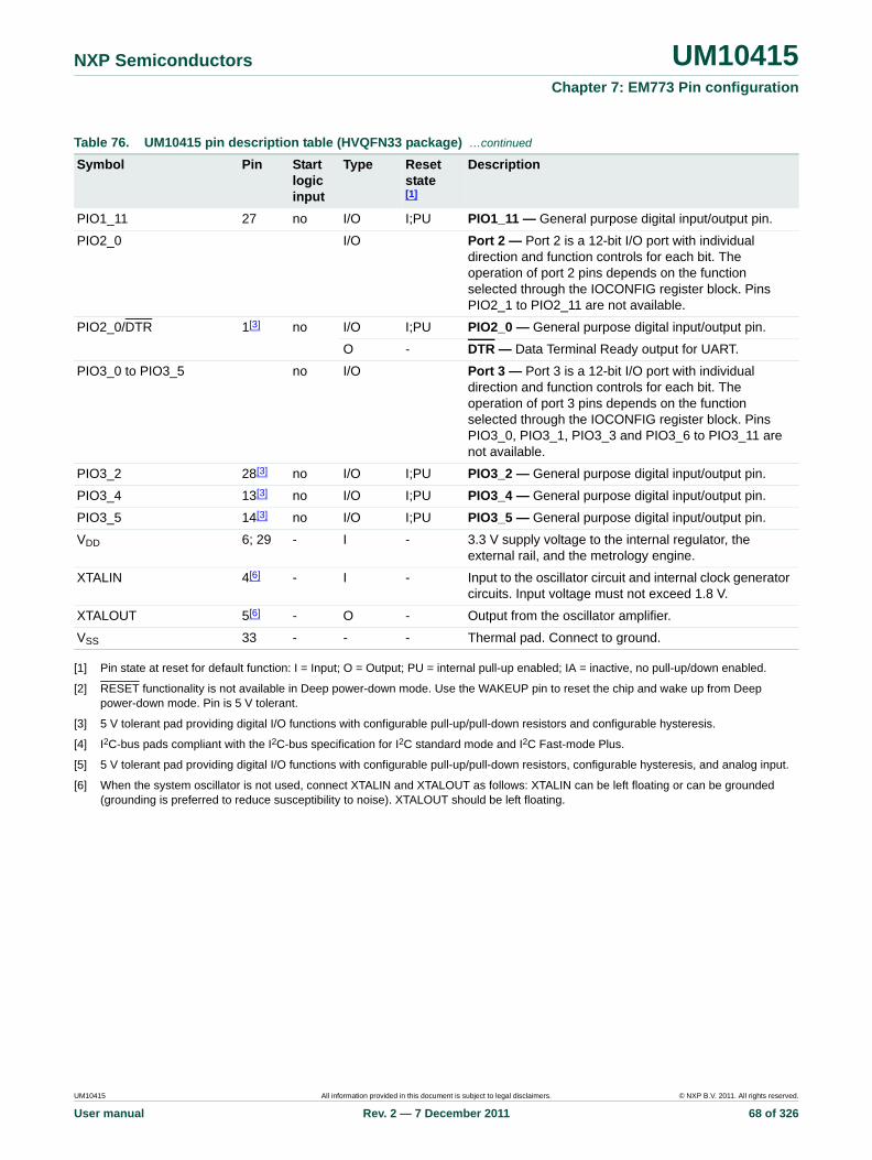
NXP Semiconductors UM10415Chapter 7: EM773 Pin configuration
[1] Pin state at reset for default function: I = Input; O = Output; PU = internal pull-up enabled; IA = inactive, no pull-up/down enabled.
[2] RESET functionality is not available in Deep power-down mode. Use the WAKEUP pin to reset the chip and wake up from Deep power-down mode. Pin is 5 V tolerant.
[3] 5 V tolerant pad providing digital I/O functions with configurable pull-up/pull-down resistors and configurable hysteresis.
[4] I2C-bus pads compliant with the I2C-bus specification for I2C standard mode and I2C Fast-mode Plus.
[5] 5 V tolerant pad providing digital I/O functions with configurable pull-up/pull-down resistors, configurable hysteresis, and analog input.
[6] When the system oscillator is not used, connect XTALIN and XTALOUT as follows: XTALIN can be left floating or can be grounded (grounding is preferred to reduce susceptibility to noise). XTALOUT should be left floating.
PIO1_11 27 no I/O I;PU PIO1_11 — General purpose digital input/output pin.
PIO2_0 I/O Port 2 — Port 2 is a 12-bit I/O port with individual direction and function controls for each bit. The operation of port 2 pins depends on the function selected through the IOCONFIG register block. Pins PIO2_1 to PIO2_11 are not available.
PIO2_0/DTR 1[3] no I/O I;PU PIO2_0 — General purpose digital input/output pin.
O - DTR — Data Terminal Ready output for UART.
PIO3_0 to PIO3_5 no I/O Port 3 — Port 3 is a 12-bit I/O port with individual direction and function controls for each bit. The operation of port 3 pins depends on the function selected through the IOCONFIG register block. Pins PIO3_0, PIO3_1, PIO3_3 and PIO3_6 to PIO3_11 are not available.
PIO3_2 28[3] no I/O I;PU PIO3_2 — General purpose digital input/output pin.
PIO3_4 13[3] no I/O I;PU PIO3_4 — General purpose digital input/output pin.
PIO3_5 14[3] no I/O I;PU PIO3_5 — General purpose digital input/output pin.
VDD 6; 29 - I - 3.3 V supply voltage to the internal regulator, the external rail, and the metrology engine.
XTALIN 4[6] - I - Input to the oscillator circuit and internal clock generator circuits. Input voltage must not exceed 1.8 V.
XTALOUT 5[6] - O - Output from the oscillator amplifier.
VSS 33 - - - Thermal pad. Connect to ground.
Table 76. UM10415 pin description table (HVQFN33 package) …continued
Symbol Pin Start logic input
Type Reset state[1]
Description
UM10415 All information provided in this document is subject to legal disclaimers. © NXP B.V. 2011. All rights reserved.
User manual Rev. 2 — 7 December 2011 68 of 326
8.1 How to read this chapter
The number of GPIO pins available on each port depends on the EM773 part and the package. See Table 77 for available GPIO pins:
Register bits corresponding to PIOn_m pins which are not available are reserved.
8.2 Introduction
8.2.1 Features
• GPIO pins can be configured as input or output by software.
• Each individual port pin can serve as an edge or level-sensitive interrupt request.
• Interrupts can be configured on single falling or rising edges and on both edges.
• Level-sensitive interrupt pins can be HIGH or LOW-active.
• All GPIO pins are inputs by default.
• Reading and writing of data registers are masked by address bits 13:2.
8.3 Register description
Each GPIO register can be up to 12 bits wide and can be read or written using word or half-word operations at word addresses.
UM10415Chapter 8: EM773 General Purpose I/O (GPIO)Rev. 2 — 7 December 2011 User manual
Table 77. GPIO configuration
Part Package GPIO port 0 GPIO port 1 GPIO port 2 GPIO port 3 Total GPIO pins
EM773 HVQFN33 PIO0_0 to PIO0_11 PIO1_0 to PIO1_11 PIO2_0 PIO3_2; PIO3_4; PIO3_5 28
Table 78. Register overview: GPIO (base address port 0: 0x5000 0000; port 1: 0x5001 0000, port 2: 0x5002 0000; port 3: 0x5003 0000)
Name Access Address offset Description Reset value
GPIOnDATA R/W 0x0000 to 0x3FF8 Port n data address masking register locations for pins PIOn_0 to PIOn_11 (see Section 8.4.1).
n/a
GPIOnDATA R/W 0x3FFC Port n data register for pins PIOn_0 to PIOn_11
n/a
- - 0x4000 to 0x7FFC reserved -
GPIOnDIR R/W 0x8000 Data direction register for port n 0x00
GPIOnIS R/W 0x8004 Interrupt sense register for port n 0x00
GPIOnIBE R/W 0x8008 Interrupt both edges register for port n 0x00
GPIOnIEV R/W 0x800C Interrupt event register for port n 0x00
GPIOnIE R/W 0x8010 Interrupt mask register for port n 0x00
UM10415 All information provided in this document is subject to legal disclaimers. © NXP B.V. 2011. All rights reserved.
User manual Rev. 2 — 7 December 2011 69 of 326

NXP Semiconductors UM10415Chapter 8: EM773 General Purpose I/O (GPIO)
8.3.1 GPIO data register
The GPIOnDATA register holds the current logic state of the pin (HIGH or LOW), independently of whether the pin is configured as an GPIO input or output or as another digital function. If the pin is configured as GPIO output, the current value of the GPIOnDATA register is driven to the pin.
A read of the GPIOnDATA register always returns the current logic level (state) of the pin independently of its configuration. Because there is a single data register for both the value of the output driver and the state of the pin’s input, write operations have different effects depending on the pin’s configuration:
• If a pin is configured as GPIO input, a write to the GPIOnDATA register has no effect on the pin level. A read returns the current state of the pin.
• If a pin is configured as GPIO output, the current value of GPIOnDATA register is driven to the pin. This value can be a result of writing to the GPIOnDATA register, or it can reflect the previous state of the pin if the pin is switched to GPIO output from GPIO input or another digital function. A read returns the current state of the pin.
• If a pin is configured as another digital function (input or output), a write to the GPIOnDATA register has no effect on the pin level. A read returns the current state of the pin even if it is configured as an output. This means that by reading the GPIOnDATA register, the digital output or input value of a function other than GPIO on that pin can be observed.
The following rules apply when the pins are switched from input to output:
• Pin is configured as input with a HIGH level applied:
– Change pin to output: pin drives HIGH level.
• Pin is configured as input with a LOW level applied:
– Change pin to output: pin drives LOW level.
GPIOnRIS R 0x8014 Raw interrupt status register for port n 0x00
GPIOnMIS R 0x8018 Masked interrupt status register for port n 0x00
GPIOnIC W 0x801C Interrupt clear register for port n 0x00
- - 0x8020 - 0xFFFF reserved 0x00
Table 78. Register overview: GPIO (base address port 0: 0x5000 0000; port 1: 0x5001 0000, port 2: 0x5002 0000; port 3: 0x5003 0000) …continued
Name Access Address offset Description Reset value
Table 79. GPIOnDATA register (GPIO0DATA, address 0x5000 0000 to 0x5000 3FFC; GPIO1DATA, address 0x5001 0000 to 0x5001 3FFC; GPIO2DATA, address 0x5002 0000 to 0x5002 3FFC; GPIO3DATA, address 0x5003 0000 to 0x5003 3FFC) bit description
Bit Symbol Description Reset value
Access
11:0 DATA Logic levels for pins PIOn_0 to PIOn_11. HIGH = 1, LOW = 0.
n/a R/W
31:12 - Reserved - -
UM10415 All information provided in this document is subject to legal disclaimers. © NXP B.V. 2011. All rights reserved.
User manual Rev. 2 — 7 December 2011 70 of 326

NXP Semiconductors UM10415Chapter 8: EM773 General Purpose I/O (GPIO)
The rules show that the pins mirror the current logic level. Therefore floating pins may drive an unpredictable level when switched from input to output.
8.3.2 GPIO data direction register
8.3.3 GPIO interrupt sense register
8.3.4 GPIO interrupt both edges sense register
Table 80. GPIOnDIR register (GPIO0DIR, address 0x5000 8000 to GPIO3DIR, address 0x5003 8000) bit description
Bit Symbol Value Description Reset value
Access
11:0 IO Selects pin x as input or output (x = 0 to 11). 0x00 R/W
0 Pin PIOn_x is configured as input.
1 Pin PIOn_x is configured as output.
31:12 - - Reserved - -
Table 81. GPIOnIS register (GPIO0IS, address 0x5000 8004 to GPIO3IS, address 0x5003 8004) bit description
Bit Symbol Value Description Reset value
Access
11:0 ISENSE Selects interrupt on pin x as level or edge sensitive (x = 0 to 11).
0x00 R/W
0 Interrupt on pin PIOn_x is configured as edge sensitive.
1 Interrupt on pin PIOn_x is configured as level sensitive.
31:12 - - Reserved - -
Table 82. GPIOnIBE register (GPIO0IBE, address 0x5000 8008 to GPIO3IBE, address 0x5003 8008) bit description
Bit Symbol Value Description Reset value
Access
11:0 IBE Selects interrupt on pin x to be triggered on both edges (x = 0 to 11).
0x00 R/W
0 Interrupt on pin PIOn_x is controlled through register GPIOnIEV.
1 Both edges on pin PIOn_x trigger an interrupt.
31:12 - - Reserved - -
UM10415 All information provided in this document is subject to legal disclaimers. © NXP B.V. 2011. All rights reserved.
User manual Rev. 2 — 7 December 2011 71 of 326

NXP Semiconductors UM10415Chapter 8: EM773 General Purpose I/O (GPIO)
8.3.5 GPIO interrupt event register
8.3.6 GPIO interrupt mask register
Bits set to HIGH in the GPIOnIE register allow the corresponding pins to trigger their individual interrupts and the combined GPIOnINTR line. Clearing a bit disables interrupt triggering on that pin.
8.3.7 GPIO raw interrupt status register
Bits read HIGH in the GPIOnIRS register reflect the raw (prior to masking) interrupt status of the corresponding pins indicating that all the requirements have been met before they are allowed to trigger the GPIOIE. Bits read as zero indicate that the corresponding input pins have not initiated an interrupt. The register is read-only.
Table 83. GPIOnIEV register (GPIO0IEV, address 0x5000 800C to GPIO3IEV, address 0x5003 800C) bit description
Bit Symbol Value Description Reset value
Access
11:0 IEV Selects interrupt on pin x to be triggered rising or falling edges (x = 0 to 11).
0x00 R/W
0 Depending on setting in register GPIOnIS (see Table 81), falling edges or LOW level on pin PIOn_x trigger an interrupt.
1 Depending on setting in register GPIOnIS (see Table 81), rising edges or HIGH level on pin PIOn_x trigger an interrupt.
31:12 - - Reserved - -
Table 84. GPIOnIE register (GPIO0IE, address 0x5000 8010 to GPIO3IE, address 0x5003 8010) bit description
Bit Symbol Value Description Reset value
Access
11:0 MASK Selects interrupt on pin x to be masked (x = 0 to 11). 0x00 R/W
0 Interrupt on pin PIOn_x is masked.
1 Interrupt on pin PIOn_x is not masked.
31:12 - - Reserved - -
Table 85. GPIOnIRS register (GPIO0IRS, address 0x5000 8014 to GPIO3IRS, address 0x5003 8014) bit description
Bit Symbol Value Description Reset value
Access
11:0 RAWST Raw interrupt status (x = 0 to 11). 0x00 R
0 No interrupt on pin PIOn_x.
1 Interrupt requirements met on PIOn_x.
31:12 - - Reserved - -
UM10415 All information provided in this document is subject to legal disclaimers. © NXP B.V. 2011. All rights reserved.
User manual Rev. 2 — 7 December 2011 72 of 326
NXP Semiconductors UM10415Chapter 8: EM773 General Purpose I/O (GPIO)
8.3.8 GPIO masked interrupt status register
Bits read HIGH in the GPIOnMIS register reflect the status of the input lines triggering an interrupt. Bits read as LOW indicate that either no interrupt on the corresponding input pins has been generated or that the interrupt is masked. GPIOMIS is the state of the interrupt after masking. The register is read-only.
8.3.9 GPIO interrupt clear register
This register allows software to clear edge detection for port bits that are identified as edge-sensitive in the Interrupt Sense register. This register has no effect on port bits identified as level-sensitive.
8.4 Functional description
8.4.1 Write/read data operation
In order for software to be able to set GPIO bits without affecting any other pins in a single write operation, bits [13:2] of a 14-bit wide address bus are used to create a 12-bit wide mask for write and read operations on the 12 GPIO pins for each port. Only GPIOnDATA bits masked by 1 are affected by read and write operations. The masked GPIOnDATA register can be located anywhere between address offsets 0x0000 to 0x3FFC in the GPIOn address space. Reading and writing to the GPIOnDATA register at address 0x3FFC sets all masking bits to 1.
Write operation
Table 86. GPIOnMIS register (GPIO0MIS, address 0x5000 8018 to GPIO3MIS, address 0x5003 8018) bit description
Bit Symbol Value Description Reset value
Access
11:0 MASK Selects interrupt on pin x to be masked (x = 0 to 11). 0x00 R
0 No interrupt or interrupt masked on pin PIOn_x.
1 Interrupt on PIOn_x.
31:12 - - Reserved - -
Table 87. GPIOnIC register (GPIO0IC, address 0x5000 801C to GPIO3IC, address 0x5003 801C) bit description
Bit Symbol Value Description Reset value
Access
11:0 CLR Selects interrupt on pin x to be cleared (x = 0 to 11). Clears the interrupt edge detection logic. This register is write-only.
Remark: The synchronizer between the GPIO and the NVIC blocks causes a delay of 2 clocks. It is recommended to add two NOPs after the clear of the interrupt edge detection logic before the exit of the interrupt service routine.
0x00 W
0 No effect.
1 Clears edge detection logic for pin PIOn_x.
31:12 - - Reserved - -
UM10415 All information provided in this document is subject to legal disclaimers. © NXP B.V. 2011. All rights reserved.
User manual Rev. 2 — 7 December 2011 73 of 326
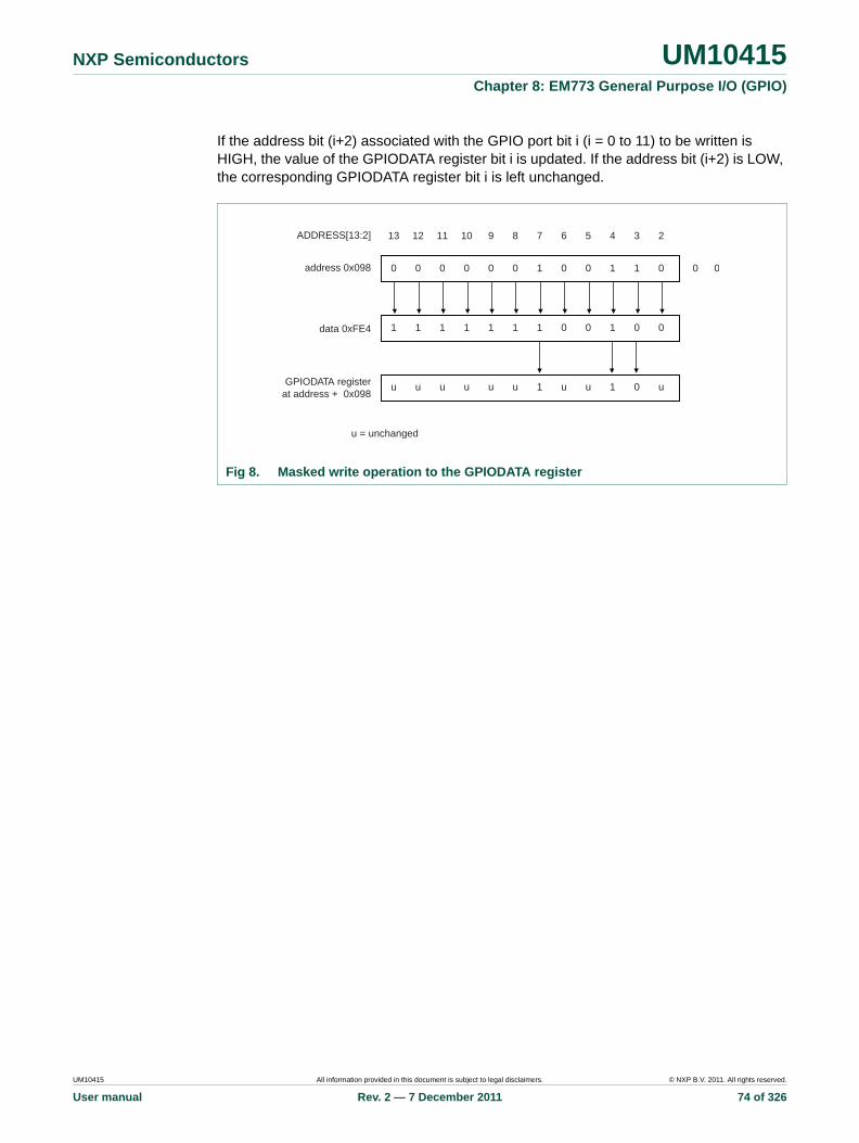
NXP Semiconductors UM10415Chapter 8: EM773 General Purpose I/O (GPIO)
If the address bit (i+2) associated with the GPIO port bit i (i = 0 to 11) to be written is HIGH, the value of the GPIODATA register bit i is updated. If the address bit (i+2) is LOW, the corresponding GPIODATA register bit i is left unchanged.
Fig 8. Masked write operation to the GPIODATA register
0 0 0 0 0 0 1 0 0 1 1 0
1 1 1 1 1 1 1 0 0 1 0 0
u u u u u u 1 u u 1 0 u
13 12 11 10 9 8 7 6 5 4 3 2
0 0
ADDRESS[13:2]
address 0x098
data 0xFE4
GPIODATA registerat address + 0x098
u = unchanged
UM10415 All information provided in this document is subject to legal disclaimers. © NXP B.V. 2011. All rights reserved.
User manual Rev. 2 — 7 December 2011 74 of 326

NXP Semiconductors UM10415Chapter 8: EM773 General Purpose I/O (GPIO)
Read operation
If the address bit associated with the GPIO data bit is HIGH, the value is read. If the address bit is LOW, the GPIO data bit is read as 0. Reading a port DATA register yields the state of port pins 11:0 ANDed with address bits 13:2.
Fig 9. Masked read operation
0 0 0 0 0 0 1 1 0 0 0 1
1 1 1 1 1 1 1 0 0 1 0 0
0 0 0 0 0 0 1 0 0 0 0 0
13 12 11 10 9 8 7 6 5 4 3 2
0 0
ADDRESS[13:2]
address 0x0C4
port pin settings
data read
UM10415 All information provided in this document is subject to legal disclaimers. © NXP B.V. 2011. All rights reserved.
User manual Rev. 2 — 7 December 2011 75 of 326
9.1 How to read this chapter
The UART block is identical for all EM773 parts.
9.2 Basic configuration
The UART is configured using the following registers:
1. Pins: The UART pins must be configured in the IOCONFIG register block (Section 6.4.1).
Remark: If the modem input pins are used, the modem function location must be also selected in the UART location registers (Section 6.4.2)
2. Power: In the SYSAHBCLKCTRL register, set bit 12 (Table 17).
3. Peripheral clock: Enable the UART peripheral clock by writing to the UARTCLKDIV register (Table 19).
9.3 Features
• 16-byte receive and transmit FIFOs.
• Register locations conform to ‘550 industry standard.
• Receiver FIFO trigger points at 1, 4, 8, and 14 bytes.
• Built-in baud rate generator.
• UART allows for implementation of either software or hardware flow control.
• RS-485/EIA-485 9-bit mode support with output enable.
• Modem control.
9.4 Pin description
UM10415Chapter 9: EM773 Universal Asynchronous Transmitter (UART)Rev. 2 — 7 December 2011 User manual
Table 88. UART pin description
Pin Type Description
RXD Input Serial Input. Serial receive data.
TXD Output Serial Output. Serial transmit data.
RTS Output Request To Send. RS-485 direction control pin.
DTR Output Data Terminal Ready.
CTS Input Clear To Send.
UM10415 All information provided in this document is subject to legal disclaimers. © NXP B.V. 2011. All rights reserved.
User manual Rev. 2 — 7 December 2011 76 of 326
NXP Semiconductors UM10415Chapter 9: EM773 Universal Asynchronous Transmitter (UART)
9.5 Clocking and power control
The UART block is gated by the AHBCLKCTRL register (see Table 17). The peripheral UART clock, which is used by the UART baud rate generator, is controlled by the UARTCLKDIV register (see Table 19).
The UART_PCLK can be disabled in the UARTCLKDIV register (see Table 19) and the UART block can be disabled through the System AHB clock control register bit 12 (see Table 17) for power savings.
9.6 Register description
The UART contains registers organized as shown in Table 89. The Divisor Latch Access Bit (DLAB) is contained in U0LCR[7] and enables access to the Divisor Latches.
Table 89. Register overview: UART (base address: 0x4000 8000)
Name Access Address offset
Description Reset Value[1]
Notes
U0RBR RO 0x000 Receiver Buffer Register. Contains the next received character to be read.
NA when DLAB=0
U0THR WO 0x000 Transmit Holding Register. The next character to be transmitted is written here.
NA when DLAB=0
U0DLL R/W 0x000 Divisor Latch LSB. Least significant byte of the baud rate divisor value. The full divisor is used to generate a baud rate from the fractional rate divider.
0x01 when DLAB=1
U0DLM R/W 0x004 Divisor Latch MSB. Most significant byte of the baud rate divisor value. The full divisor is used to generate a baud rate from the fractional rate divider.
0x00 when DLAB=1
U0IER R/W 0x004 Interrupt Enable Register. Contains individual interrupt enable bits for the 7 potential UART interrupts.
0x00 when DLAB=0
U0IIR RO 0x008 Interrupt ID Register. Identifies which interrupt(s) are pending. 0x01 -
U0FCR WO 0x008 FIFO Control Register. Controls UART FIFO usage and modes. 0x00 -
U0LCR R/W 0x00C Line Control Register. Contains controls for frame formatting and break generation.
0x00 -
U0MCR R/W 0x010 Modem control register 0x00 -
U0LSR RO 0x014 Line Status Register. Contains flags for transmit and receive status, including line errors.
0x60 -
U0MSR RO 0x018 Modem status register 0x00 -
U0SCR R/W 0x01C Scratch Pad Register. Eight-bit temporary storage for software. 0x00 -
U0ACR R/W 0x020 Auto-baud Control Register. Contains controls for the auto-baud feature.
0x00 -
- - 0x024 Reserved - -
U0FDR R/W 0x028 Fractional Divider Register. Generates a clock input for the baud rate divider.
0x10 -
- - 0x02C Reserved - -
U0TER R/W 0x030 Transmit Enable Register. Turns off UART transmitter for use with software flow control.
0x80 -
- - 0x034 - 0x048
Reserved - -
UM10415 All information provided in this document is subject to legal disclaimers. © NXP B.V. 2011. All rights reserved.
User manual Rev. 2 — 7 December 2011 77 of 326

NXP Semiconductors UM10415Chapter 9: EM773 Universal Asynchronous Transmitter (UART)
[1] Reset Value reflects the data stored in used bits only. It does not include reserved bits content.
U0RS485CTRL R/W 0x04C RS-485/EIA-485 Control. Contains controls to configure various aspects of RS-485/EIA-485 modes.
0x00 -
U0ADRMATCH R/W 0x050 RS-485/EIA-485 address match. Contains the address match value for RS-485/EIA-485 mode.
0x00 -
U0RS485DLY R/W 0x054 RS-485/EIA-485 direction control delay. 0x00 -
Table 89. Register overview: UART (base address: 0x4000 8000)
Name Access Address offset
Description Reset Value[1]
Notes
UM10415 All information provided in this document is subject to legal disclaimers. © NXP B.V. 2011. All rights reserved.
User manual Rev. 2 — 7 December 2011 78 of 326

NXP Semiconductors UM10415Chapter 9: EM773 Universal Asynchronous Transmitter (UART)
9.6.1 UART Receiver Buffer Register (U0RBR - 0x4000 8000, when DLAB = 0, Read Only)
The U0RBR is the top byte of the UART RX FIFO. The top byte of the RX FIFO contains the oldest character received and can be read via the bus interface. The LSB (bit 0) represents the “oldest” received data bit. If the character received is less than 8 bits, the unused MSBs are padded with zeroes.
The Divisor Latch Access Bit (DLAB) in U0LCR must be zero in order to access the U0RBR. The U0RBR is always Read Only.
Since PE, FE and BI bits (see Table 101) correspond to the byte sitting on the top of the RBR FIFO (i.e. the one that will be read in the next read from the RBR), the right approach for fetching the valid pair of received byte and its status bits is first to read the content of the U0LSR register, and then to read a byte from the U0RBR.
9.6.2 UART Transmitter Holding Register (U0THR - 0x4000 8000 when DLAB = 0, Write Only)
The U0THR is the top byte of the UART TX FIFO. The top byte is the newest character in the TX FIFO and can be written via the bus interface. The LSB represents the first bit to transmit.
The Divisor Latch Access Bit (DLAB) in U0LCR must be zero in order to access the U0THR. The U0THR is always Write Only.
9.6.3 UART Divisor Latch LSB and MSB Registers (U0DLL - 0x4000 8000 and U0DLM - 0x4000 8004, when DLAB = 1)
The UART Divisor Latch is part of the UART Baud Rate Generator and holds the value used, along with the Fractional Divider, to divide the UART_PCLK clock in order to produce the baud rate clock, which must be 16x the desired baud rate. The U0DLL and U0DLM registers together form a 16-bit divisor where U0DLL contains the lower 8 bits of the divisor and U0DLM contains the higher 8 bits of the divisor. A 0x0000 value is treated like a 0x0001 value as division by zero is not allowed.The Divisor Latch Access Bit (DLAB) in U0LCR must be one in order to access the UART Divisor Latches. Details on how to select the right value for U0DLL and U0DLM can be found in Section 9.6.15.
Table 90. UART Receiver Buffer Register (U0RBR - address 0x4000 8000 when DLAB = 0, Read Only) bit description
Bit Symbol Description Reset Value
7:0 RBR The UART Receiver Buffer Register contains the oldest received byte in the UART RX FIFO.
undefined
31:8 - Reserved -
Table 91. UART Transmitter Holding Register (U0THR - address 0x4000 8000 when DLAB = 0, Write Only) bit description
Bit Symbol Description Reset Value
7:0 THR Writing to the UART Transmit Holding Register causes the data to be stored in the UART transmit FIFO. The byte will be sent when it reaches the bottom of the FIFO and the transmitter is available.
NA
31:8 - Reserved -
UM10415 All information provided in this document is subject to legal disclaimers. © NXP B.V. 2011. All rights reserved.
User manual Rev. 2 — 7 December 2011 79 of 326
NXP Semiconductors UM10415Chapter 9: EM773 Universal Asynchronous Transmitter (UART)
9.6.4 UART Interrupt Enable Register (U0IER - 0x4000 8004, when DLAB = 0)
The U0IER is used to enable the four UART interrupt sources.
Table 92. UART Divisor Latch LSB Register (U0DLL - address 0x4000 8000 when DLAB = 1) bit description
Bit Symbol Description Reset value
7:0 DLLSB The UART Divisor Latch LSB Register, along with the U0DLM register, determines the baud rate of the UART.
0x01
31:8 - Reserved -
Table 93. UART Divisor Latch MSB Register (U0DLM - address 0x4000 8004 when DLAB = 1) bit description
Bit Symbol Description Reset value
7:0 DLMSB The UART Divisor Latch MSB Register, along with the U0DLL register, determines the baud rate of the UART.
0x00
31:8 - Reserved -
Table 94. UART Interrupt Enable Register (U0IER - address 0x4000 8004 when DLAB = 0) bit description
Bit Symbol Value Description Reset value
0 RBR Interrupt Enable
Enables the Receive Data Available interrupt for UART. It also controls the Character Receive Time-out interrupt.
0
0 Disable the RDA interrupt.
1 Enable the RDA interrupt.
1 THRE Interrupt Enable
Enables the THRE interrupt for UART. The status of this interrupt can be read from U0LSR[5].
0
0 Disable the THRE interrupt.
1 Enable the THRE interrupt.
2 RX Line Interrupt Enable
Enables the UART RX line status interrupts. The status of this interrupt can be read from U0LSR[4:1].
0
0 Disable the RX line status interrupts.
1 Enable the RX line status interrupts.
3 - - Reserved -
6:4 - Reserved, user software should not write ones to reserved bits. The value read from a reserved bit is not defined.
NA
7 - - Reserved 0
8 ABEOIntEn Enables the end of auto-baud interrupt. 0
0 Disable end of auto-baud Interrupt.
1 Enable end of auto-baud Interrupt.
9 ABTOIntEn Enables the auto-baud time-out interrupt. 0
0 Disable auto-baud time-out Interrupt.
1 Enable auto-baud time-out Interrupt.
31:10 - Reserved, user software should not write ones to reserved bits. The value read from a reserved bit is not defined.
NA
UM10415 All information provided in this document is subject to legal disclaimers. © NXP B.V. 2011. All rights reserved.
User manual Rev. 2 — 7 December 2011 80 of 326

NXP Semiconductors UM10415Chapter 9: EM773 Universal Asynchronous Transmitter (UART)
9.6.5 UART Interrupt Identification Register (U0IIR - 0x4004 8008, Read Only)
U0IIR provides a status code that denotes the priority and source of a pending interrupt. The interrupts are frozen during a U0IIR access. If an interrupt occurs during a U0IIR access, the interrupt is recorded for the next U0IIR access.
Bits U0IIR[9:8] are set by the auto-baud function and signal a time-out or end of auto-baud condition. The auto-baud interrupt conditions are cleared by setting the corresponding Clear bits in the Auto-baud Control Register.
If the IntStatus bit is one and no interrupt is pending and the IntId bits will be zero. If the IntStatus is 0, a non auto-baud interrupt is pending in which case the IntId bits identify the type of interrupt and handling as described in Table 96. Given the status of U0IIR[3:0], an interrupt handler routine can determine the cause of the interrupt and how to clear the active interrupt. The U0IIR must be read in order to clear the interrupt prior to exiting the Interrupt Service Routine.
The UART RLS interrupt (U0IIR[3:1] = 011) is the highest priority interrupt and is set whenever any one of four error conditions occur on the UART RX input: overrun error (OE), parity error (PE), framing error (FE) and break interrupt (BI). The UART Rx error condition that set the interrupt can be observed via U0LSR[4:1]. The interrupt is cleared upon a U0LSR read.
Table 95. UART Interrupt Identification Register (U0IIR - address 0x4004 8008, Read Only) bit description
Bit Symbol Value Description Reset value
0 IntStatus Interrupt status. Note that U0IIR[0] is active low. The pending interrupt can be determined by evaluating U0IIR[3:1].
1
0 At least one interrupt is pending.
1 No interrupt is pending.
3:1 IntId Interrupt identification. U0IER[3:1] identifies an interrupt corresponding to the UART Rx FIFO. All other combinations of U0IER[3:1] not listed below are reserved (100,101,111).
0
011 1 - Receive Line Status (RLS).
010 2a - Receive Data Available (RDA).
110 2b - Character Time-out Indicator (CTI).
001 3 - THRE Interrupt.
000 4 - Modem interrupt.
5:4 - Reserved, user software should not write ones to reserved bits. The value read from a reserved bit is not defined.
NA
7:6 FIFO Enable These bits are equivalent to U0FCR[0]. 0
8 ABEOInt End of auto-baud interrupt. True if auto-baud has finished successfully and interrupt is enabled.
0
9 ABTOInt Auto-baud time-out interrupt. True if auto-baud has timed out and interrupt is enabled.
0
31:10 - Reserved, user software should not write ones to reserved bits. The value read from a reserved bit is not defined.
NA
UM10415 All information provided in this document is subject to legal disclaimers. © NXP B.V. 2011. All rights reserved.
User manual Rev. 2 — 7 December 2011 81 of 326

NXP Semiconductors UM10415Chapter 9: EM773 Universal Asynchronous Transmitter (UART)
The UART RDA interrupt (U0IIR[3:1] = 010) shares the second level priority with the CTI interrupt (U0IIR[3:1] = 110). The RDA is activated when the UART Rx FIFO reaches the trigger level defined in U0FCR7:6 and is reset when the UART Rx FIFO depth falls below the trigger level. When the RDA interrupt goes active, the CPU can read a block of data defined by the trigger level.
The CTI interrupt (U0IIR[3:1] = 110) is a second level interrupt and is set when the UART Rx FIFO contains at least one character and no UART Rx FIFO activity has occurred in 3.5 to 4.5 character times. Any UART Rx FIFO activity (read or write of UART RSR) will clear the interrupt. This interrupt is intended to flush the UART RBR after a message has been received that is not a multiple of the trigger level size. For example, if a peripheral wished to send a 105 character message and the trigger level was 10 characters, the CPU would receive 10 RDA interrupts resulting in the transfer of 100 characters and 1 to 5 CTI interrupts (depending on the service routine) resulting in the transfer of the remaining 5 characters.
[1] Values “0000”, “0011”, “0101”, “0111”, “1000”, “1001”, “1010”, “1011”,”1101”,”1110”,”1111” are reserved.
[2] For details see Section 9.6.9 “UART Line Status Register (U0LSR - 0x4000 8014, Read Only)”
[3] For details see Section 9.6.1 “UART Receiver Buffer Register (U0RBR - 0x4000 8000, when DLAB = 0, Read Only)”
[4] For details see Section 9.6.5 “UART Interrupt Identification Register (U0IIR - 0x4004 8008, Read Only)” and Section 9.6.2 “UART Transmitter Holding Register (U0THR - 0x4000 8000 when DLAB = 0, Write Only)”
The UART THRE interrupt (U0IIR[3:1] = 001) is a third level interrupt and is activated when the UART THR FIFO is empty provided certain initialization conditions have been met. These initialization conditions are intended to give the UART THR FIFO a chance to fill up with data to eliminate many THRE interrupts from occurring at system start-up. The
Table 96. UART Interrupt Handling
U0IIR[3:0] value[1]
Priority Interrupt type
Interrupt source Interrupt reset
0001 - None None -
0110 Highest RX Line Status / Error
OE[2] or PE[2] or FE[2] or BI[2] U0LSR Read[2]
0100 Second RX Data Available
Rx data available or trigger level reached in FIFO (U0FCR0=1)
U0RBR Read[3] or UART FIFO drops below trigger level
1100 Second Character Time-out indication
Minimum of one character in the RX FIFO and no character input or removed during a time period depending on how many characters are in FIFO and what the trigger level is set at (3.5 to 4.5 character times).
The exact time will be:
[(word length) 7 - 2] 8 + [(trigger level - number of characters) 8 + 1] RCLKs
U0RBR Read[3]
0010 Third THRE THRE[2] U0IIR Read[4] (if source of interrupt) or THR write
UM10415 All information provided in this document is subject to legal disclaimers. © NXP B.V. 2011. All rights reserved.
User manual Rev. 2 — 7 December 2011 82 of 326

NXP Semiconductors UM10415Chapter 9: EM773 Universal Asynchronous Transmitter (UART)
initialization conditions implement a one character delay minus the stop bit whenever THRE = 1 and there have not been at least two characters in the U0THR at one time since the last THRE = 1 event. This delay is provided to give the CPU time to write data to U0THR without a THRE interrupt to decode and service. A THRE interrupt is set immediately if the UART THR FIFO has held two or more characters at one time and currently, the U0THR is empty. The THRE interrupt is reset when a U0THR write occurs or a read of the U0IIR occurs and the THRE is the highest interrupt (U0IIR[3:1] = 001).
9.6.6 UART FIFO Control Register (U0FCR - 0x4000 8008, Write Only)
The U0FCR controls the operation of the UART RX and TX FIFOs.
9.6.7 UART Line Control Register (U0LCR - 0x4000 800C)
The U0LCR determines the format of the data character that is to be transmitted or received.
Table 97. UART FIFO Control Register (U0FCR - address 0x4000 8008, Write Only) bit description
Bit Symbol Value Description Reset value
0 FIFO Enable
0 UART FIFOs are disabled. Must not be used in the application. 0
1 Active high enable for both UART Rx and TX FIFOs and U0FCR[7:1] access. This bit must be set for proper UART operation. Any transition on this bit will automatically clear the UART FIFOs.
1 RX FIFO Reset
0 No impact on either of UART FIFOs. 0
1 Writing a logic 1 to U0FCR[1] will clear all bytes in UART Rx FIFO, reset the pointer logic. This bit is self-clearing.
2 TX FIFO Reset
0 No impact on either of UART FIFOs. 0
1 Writing a logic 1 to U0FCR[2] will clear all bytes in UART TX FIFO, reset the pointer logic. This bit is self-clearing.
3 - - Reserved 0
5:4 - Reserved, user software should not write ones to reserved bits. The value read from a reserved bit is not defined.
NA
7:6 RX Trigger Level
These two bits determine how many receiver UART FIFO characters must be written before an interrupt is activated.
0
00 Trigger level 0 (1 character or 0x01).
01 Trigger level 1 (4 characters or 0x04).
10 Trigger level 2 (8 characters or 0x08).
11 Trigger level 3 (14 characters or 0x0E).
31:8 - - Reserved -
Table 98. UART Line Control Register (U0LCR - address 0x4000 800C) bit description
Bit Symbol Value Description Reset Value
1:0 Word Length Select
00 5-bit character length. 0
01 6-bit character length.
10 7-bit character length.
11 8-bit character length.
UM10415 All information provided in this document is subject to legal disclaimers. © NXP B.V. 2011. All rights reserved.
User manual Rev. 2 — 7 December 2011 83 of 326

NXP Semiconductors UM10415Chapter 9: EM773 Universal Asynchronous Transmitter (UART)
9.6.8 UART Modem Control Register
The U0MCR enables the modem loopback mode and controls the modem output signals.
2 Stop Bit Select
0 1 stop bit. 0
1 2 stop bits (1.5 if U0LCR[1:0]=00).
3 Parity Enable
0 Disable parity generation and checking. 0
1 Enable parity generation and checking.
5:4 Parity Select
00 Odd parity. Number of 1s in the transmitted character and the attached parity bit will be odd.
0
01 Even Parity. Number of 1s in the transmitted character and the attached parity bit will be even.
10 Forced "1" stick parity.
11 Forced "0" stick parity.
6 Break Control
0 Disable break transmission. 0
1 Enable break transmission. Output pin UART TXD is forced to logic 0 when U0LCR[6] is active high.
7 Divisor Latch Access Bit (DLAB)
0 Disable access to Divisor Latches. 0
1 Enable access to Divisor Latches.
31:8
- - Reserved -
Table 98. UART Line Control Register (U0LCR - address 0x4000 800C) bit description
Bit Symbol Value Description Reset Value
Table 99. UART0 Modem Control Register (U0MCR - address 0x4000 8010) bit description
Bit Symbol Value Description Reset value
0 DTR Control
Source for modem output pin, DTR. This bit reads as 0 when modem loopback mode is active.
0
1 RTS Control
Source for modem output pin RTS. This bit reads as 0 when modem loopback mode is active.
0
3:2 - NA Reserved, user software should not write ones to reserved bits. The value read from a reserved bit is not defined.
0
UM10415 All information provided in this document is subject to legal disclaimers. © NXP B.V. 2011. All rights reserved.
User manual Rev. 2 — 7 December 2011 84 of 326
NXP Semiconductors UM10415Chapter 9: EM773 Universal Asynchronous Transmitter (UART)
9.6.8.1 Auto-flow control
If auto-RTS mode is enabled the UART‘s receiver FIFO hardware controls the RTS output of the UART. If the auto-CTS mode is enabled the UART‘s U0TSR hardware will only start transmitting if the CTS input signal is asserted.
9.6.8.1.1 Auto-RTS
The auto-RTS function is enabled by setting the RTSen bit. Auto-RTS data flow control originates in the U0RBR module and is linked to the programmed receiver FIFO trigger level. If auto-RTS is enabled, the data-flow is controlled as follows:
When the receiver FIFO level reaches the programmed trigger level, RTS is deasserted (to a high value). It is possible that the sending UART sends an additional byte after the trigger level is reached (assuming the sending UART has another byte to send) because it might not recognize the deassertion of RTS until after it has begun sending the additional byte. RTS is automatically reasserted (to a low value) once the receiver FIFO has reached the previous trigger level. The reassertion of RTS signals the sending UART to continue transmitting data.
If Auto-RTS mode is disabled, the RTSen bit controls the RTS output of the UART. If Auto-RTS mode is enabled, hardware controls the RTS output, and the actual value of RTS will be copied in the RTS Control bit of the UART. As long as Auto-RTS is enabled, the value of the RTS Control bit is read-only for software.
4 Loopback Mode Select
0
The modem loopback mode provides a mechanism to perform diagnostic loopback testing. Serial data from the transmitter is connected internally to serial input of the receiver. Input pin, RXD, has no effect on loopback and output pin, TXD is held in marking state. The four modem inputs (CTS, DSR, RI and DCD) are disconnected externally. Externally, the modem outputs (RTS, DTR) are set inactive. Internally, the four modem outputs are connected to the four modem inputs. As a result of these connections, the upper four bits of the U0MSR will be driven by the lower four bits of the U0MCR rather than the four modem inputs in normal mode. This permits modem status interrupts to be generated in loopback mode by writing the lower four bits of U0MCR.
0
Disable modem loopback mode.
1 Enable modem loopback mode.
5 - NA Reserved, user software should not write ones to reserved bits. The value read from a reserved bit is not defined.
0
6 RTSen 0 Disable auto-rts flow control. 0
1 Enable auto-rts flow control.
7 CTSen 0 Disable auto-cts flow control. 0
1 Enable auto-cts flow control.
31:8 - - Reserved -
Table 99. UART0 Modem Control Register (U0MCR - address 0x4000 8010) bit description
Bit Symbol Value Description Reset value
UM10415 All information provided in this document is subject to legal disclaimers. © NXP B.V. 2011. All rights reserved.
User manual Rev. 2 — 7 December 2011 85 of 326
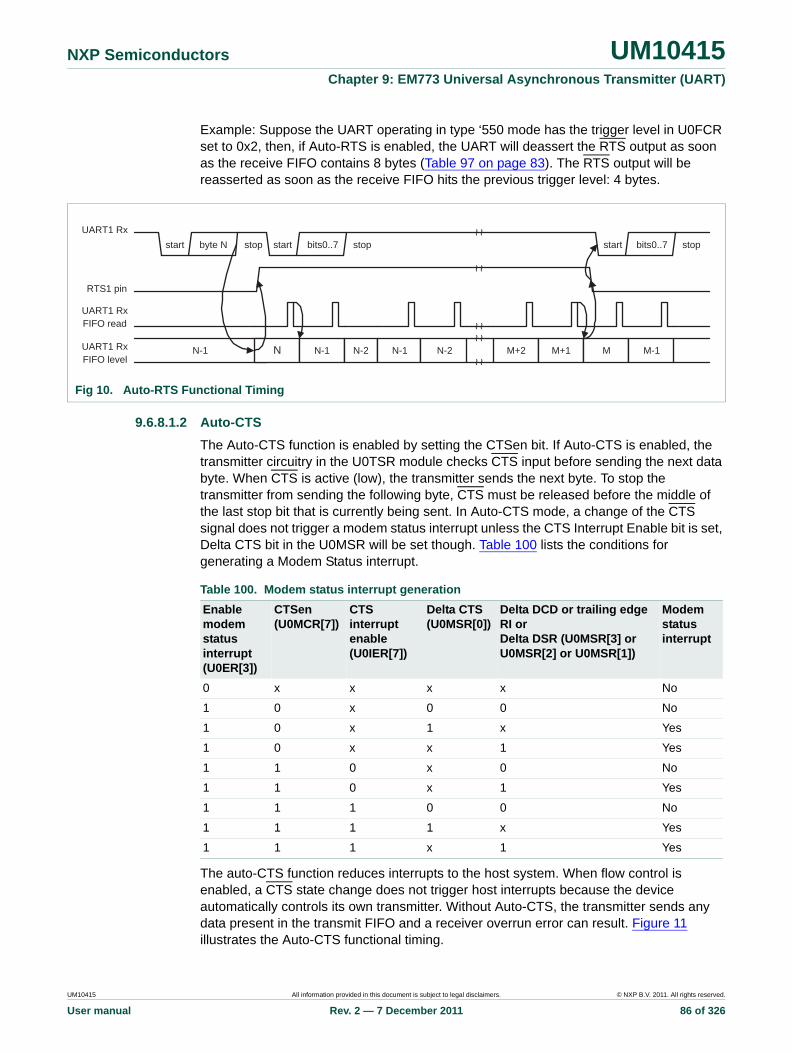
NXP Semiconductors UM10415Chapter 9: EM773 Universal Asynchronous Transmitter (UART)
Example: Suppose the UART operating in type ‘550 mode has the trigger level in U0FCR set to 0x2, then, if Auto-RTS is enabled, the UART will deassert the RTS output as soon as the receive FIFO contains 8 bytes (Table 97 on page 83). The RTS output will be reasserted as soon as the receive FIFO hits the previous trigger level: 4 bytes.
9.6.8.1.2 Auto-CTS
The Auto-CTS function is enabled by setting the CTSen bit. If Auto-CTS is enabled, the transmitter circuitry in the U0TSR module checks CTS input before sending the next data byte. When CTS is active (low), the transmitter sends the next byte. To stop the transmitter from sending the following byte, CTS must be released before the middle of the last stop bit that is currently being sent. In Auto-CTS mode, a change of the CTS signal does not trigger a modem status interrupt unless the CTS Interrupt Enable bit is set, Delta CTS bit in the U0MSR will be set though. Table 100 lists the conditions for generating a Modem Status interrupt.
The auto-CTS function reduces interrupts to the host system. When flow control is enabled, a CTS state change does not trigger host interrupts because the device automatically controls its own transmitter. Without Auto-CTS, the transmitter sends any data present in the transmit FIFO and a receiver overrun error can result. Figure 11 illustrates the Auto-CTS functional timing.
Fig 10. Auto-RTS Functional Timing
start byte N stop start bits0..7 stop start bits0..7 stop
N-1 N N-1 N-1N-2 N-2 M+2 M+1 M M-1
UART1 Rx
RTS1 pin
UART1 RxFIFO level
UART1 RxFIFO read
~ ~~ ~
~ ~~ ~
~ ~
Table 100. Modem status interrupt generation
Enable modem status interrupt (U0ER[3])
CTSen (U0MCR[7])
CTS interrupt enable (U0IER[7])
Delta CTS (U0MSR[0])
Delta DCD or trailing edge RI or Delta DSR (U0MSR[3] or U0MSR[2] or U0MSR[1])
Modem status interrupt
0 x x x x No
1 0 x 0 0 No
1 0 x 1 x Yes
1 0 x x 1 Yes
1 1 0 x 0 No
1 1 0 x 1 Yes
1 1 1 0 0 No
1 1 1 1 x Yes
1 1 1 x 1 Yes
UM10415 All information provided in this document is subject to legal disclaimers. © NXP B.V. 2011. All rights reserved.
User manual Rev. 2 — 7 December 2011 86 of 326

NXP Semiconductors UM10415Chapter 9: EM773 Universal Asynchronous Transmitter (UART)
While starting transmission of the initial character, the CTS signal is asserted. Transmission will stall as soon as the pending transmission has completed. The UART will continue transmitting a 1 bit as long as CTS is de-asserted (high). As soon as CTS gets de-asserted, transmission resumes and a start bit is sent followed by the data bits of the next character.
9.6.9 UART Line Status Register (U0LSR - 0x4000 8014, Read Only)
The U0LSR is a Read Only register that provides status information on the UART TX and RX blocks.
Fig 11. Auto-CTS Functional Timing
start bits0..7 start bits0..7 stop start bits0..7 stop
UART1 TX
CTS1 pin
~ ~~ ~
~ ~~ ~
stop
Table 101. UART Line Status Register (U0LSR - address 0x4000 8014, Read Only) bit description
Bit Symbol Value Description Reset Value
0 Receiver Data Ready(RDR)
Receiver Data Ready:U0LSR[0] is set when the U0RBR holds an unread character and is cleared when the UART RBR FIFO is empty.
0
0 U0RBR is empty.
1 U0RBR contains valid data.
1 Overrun Error (OE)
The overrun error condition is set as soon as it occurs. A U0LSR read clears U0LSR[1]. U0LSR[1] is set when UART RSR has a new character assembled and the UART RBR FIFO is full. In this case, the UART RBR FIFO will not be overwritten and the character in the UART RSR will be lost.
0
0 Overrun error status is inactive.
1 Overrun error status is active.
2 Parity Error (PE)
When the parity bit of a received character is in the wrong state, a parity error occurs. A U0LSR read clears U0LSR[2]. Time of parity error detection is dependent on U0FCR[0].
Note: A parity error is associated with the character at the top of the UART RBR FIFO.
0
0 Parity error status is inactive.
1 Parity error status is active.
UM10415 All information provided in this document is subject to legal disclaimers. © NXP B.V. 2011. All rights reserved.
User manual Rev. 2 — 7 December 2011 87 of 326
NXP Semiconductors UM10415Chapter 9: EM773 Universal Asynchronous Transmitter (UART)
9.6.10 UART Modem Status Register
The U0MSR is a read-only register that provides status information on the modem input signals. U0MSR[3:0] is cleared on U0MSR read. Note that modem signals have no direct effect on the UART operation. They facilitate the software implementation of modem signal operations.
3 Framing Error (FE)
When the stop bit of a received character is a logic 0, a framing error occurs. A U0LSR read clears U0LSR[3]. The time of the framing error detection is dependent on U0FCR0. Upon detection of a framing error, the RX will attempt to re-synchronize to the data and assume that the bad stop bit is actually an early start bit. However, it cannot be assumed that the next received byte will be correct even if there is no Framing Error.
Note: A framing error is associated with the character at the top of the UART RBR FIFO.
0
0 Framing error status is inactive.
1 Framing error status is active.
4 Break Interrupt (BI)
When RXD1 is held in the spacing state (all zeros) for one full character transmission (start, data, parity, stop), a break interrupt occurs. Once the break condition has been detected, the receiver goes idle until RXD1 goes to marking state (all ones). A U0LSR read clears this status bit. The time of break detection is dependent on U0FCR[0].
Note: The break interrupt is associated with the character at the top of the UART RBR FIFO.
0
0 Break interrupt status is inactive.
1 Break interrupt status is active.
5 Transmitter Holding Register Empty (THRE)
THRE is set immediately upon detection of an empty UART THR and is cleared on a U0THR write.
1
0 U0THR contains valid data.
1 U0THR is empty.
6 Transmitter Empty (TEMT)
TEMT is set when both U0THR and U0TSR are empty; TEMT is cleared when either the U0TSR or the U0THR contain valid data.
1
0 U0THR and/or the U0TSR contains valid data.
1 U0THR and the U0TSR are empty.
7 Error in RX FIFO (RXFE)
U0LSR[7] is set when a character with a RX error such as framing error, parity error or break interrupt, is loaded into the U0RBR. This bit is cleared when the U0LSR register is read and there are no subsequent errors in the UART FIFO.
0
0 U0RBR contains no UART RX errors or U0FCR[0]=0.
1 UART RBR contains at least one UART RX error.
31:8
- - Reserved -
Table 101. UART Line Status Register (U0LSR - address 0x4000 8014, Read Only) bit description …continued
Bit Symbol Value Description Reset Value
UM10415 All information provided in this document is subject to legal disclaimers. © NXP B.V. 2011. All rights reserved.
User manual Rev. 2 — 7 December 2011 88 of 326

NXP Semiconductors UM10415Chapter 9: EM773 Universal Asynchronous Transmitter (UART)
9.6.11 UART Scratch Pad Register (U0SCR - 0x4000 801C)
The U0SCR has no effect on the UART operation. This register can be written and/or read at user’s discretion. There is no provision in the interrupt interface that would indicate to the host that a read or write of the U0SCR has occurred.
9.6.12 UART Auto-baud Control Register (U0ACR - 0x4000 8020)
The UART Auto-baud Control Register (U0ACR) controls the process of measuring the incoming clock/data rate for the baud rate generation and can be read and written at user’s discretion.
Table 102. UART Modem Status Register (U0MSR - address 0x4000 8018) bit description
Bit Symbol Value Description Reset Value
0 Delta CTS 0
Set upon state change of input CTS. Cleared on a U0MSR read. 0
No change detected on modem input CTS.
1 State change detected on modem input CTS.
1 Delta DSR 0
Set upon state change of input DSR. Cleared on a U0MSR read. 0
No change detected on modem input DSR.
1 State change detected on modem input DSR.
2 Trailing Edge RI
0
Set upon low to high transition of input RI. Cleared on a U0MSR read.
0
No change detected on modem input, RI.
1 Low-to-high transition detected on RI.
3 Delta DCD 0
Set upon state change of input DCD. Cleared on a U0MSR read. 0
No change detected on modem input DCD.
1 State change detected on modem input DCD.
4 CTS Clear To Send State. Complement of input signal CTS. This bit is connected to U0MCR[1] in modem loopback mode.
0
5 DSR Data Set Ready State. Complement of input signal DSR. This bit is connected to U0MCR[0] in modem loopback mode.
0
6 RI Ring Indicator State. Complement of input RI. This bit is connected to U0MCR[2] in modem loopback mode.
0
7 DCD Data Carrier Detect State. Complement of input DCD. This bit is connected to U0MCR[3] in modem loopback mode.
0
31:8
- - Reserved -
Table 103. UART Scratch Pad Register (U0SCR - address 0x4000 8014) bit description
Bit Symbol Description Reset Value
7:0 Pad A readable, writable byte. 0x00
31:8
- Reserved -
UM10415 All information provided in this document is subject to legal disclaimers. © NXP B.V. 2011. All rights reserved.
User manual Rev. 2 — 7 December 2011 89 of 326

NXP Semiconductors UM10415Chapter 9: EM773 Universal Asynchronous Transmitter (UART)
9.6.13 Auto-baud
The UART auto-baud function can be used to measure the incoming baud rate based on the ”AT" protocol (Hayes command). If enabled the auto-baud feature will measure the bit time of the receive data stream and set the divisor latch registers U0DLM and U0DLL accordingly.
Auto-baud is started by setting the U0ACR Start bit. Auto-baud can be stopped by clearing the U0ACR Start bit. The Start bit will clear once auto-baud has finished and reading the bit will return the status of auto-baud (pending/finished).
Two auto-baud measuring modes are available which can be selected by the U0ACR Mode bit. In Mode 0 the baud rate is measured on two subsequent falling edges of the UART Rx pin (the falling edge of the start bit and the falling edge of the least significant bit). In Mode 1 the baud rate is measured between the falling edge and the subsequent rising edge of the UART Rx pin (the length of the start bit).
Table 104. Auto-baud Control Register (U0ACR - address 0x4000 8020) bit description
Bit Symbol Value Description Reset value
0 Start This bit is automatically cleared after auto-baud completion.
0
0 Auto-baud stop (auto-baud is not running).
1 Auto-baud start (auto-baud is running). Auto-baud run bit. This bit is automatically cleared after auto-baud completion.
1 Mode Auto-baud mode select bit. 0
0 Mode 0.
1 Mode 1.
2 AutoRestart 0 No restart 0
1 Restart in case of time-out (counter restarts at next UART Rx falling edge)
0
7:3 - NA Reserved, user software should not write ones to reserved bits. The value read from a reserved bit is not defined.
0
8 ABEOIntClr End of auto-baud interrupt clear bit (write only accessible).
0
0 Writing a 0 has no impact.
1 Writing a 1 will clear the corresponding interrupt in the U0IIR.
9 ABTOIntClr Auto-baud time-out interrupt clear bit (write only accessible).
0
0 Writing a 0 has no impact.
1 Writing a 1 will clear the corresponding interrupt in the U0IIR.
31:10 - NA Reserved, user software should not write ones to reserved bits. The value read from a reserved bit is not defined.
0
UM10415 All information provided in this document is subject to legal disclaimers. © NXP B.V. 2011. All rights reserved.
User manual Rev. 2 — 7 December 2011 90 of 326
NXP Semiconductors UM10415Chapter 9: EM773 Universal Asynchronous Transmitter (UART)
The U0ACR AutoRestart bit can be used to automatically restart baud rate measurement if a time-out occurs (the rate measurement counter overflows). If this bit is set, the rate measurement will restart at the next falling edge of the UART Rx pin.
The auto-baud function can generate two interrupts.
• The U0IIR ABTOInt interrupt will get set if the interrupt is enabled (U0IER ABToIntEn is set and the auto-baud rate measurement counter overflows).
• The U0IIR ABEOInt interrupt will get set if the interrupt is enabled (U0IER ABEOIntEn is set and the auto-baud has completed successfully).
The auto-baud interrupts have to be cleared by setting the corresponding U0ACR ABTOIntClr and ABEOIntEn bits.
The fractional baud rate generator must be disabled (DIVADDVAL = 0) during auto-baud. Also, when auto-baud is used, any write to U0DLM and U0DLL registers should be done before U0ACR register write. The minimum and the maximum baud rates supported by UART are function of UART_PCLK, number of data bits, stop bits and parity bits.
(2)
9.6.14 Auto-baud modes
When the software is expecting an ”AT" command, it configures the UART with the expected character format and sets the U0ACR Start bit. The initial values in the divisor latches U0DLM and U0DLM don‘t care. Because of the ”A" or ”a" ASCII coding (”A" = 0x41, ”a" = 0x61), the UART Rx pin sensed start bit and the LSB of the expected character are delimited by two falling edges. When the U0ACR Start bit is set, the auto-baud protocol will execute the following phases:
1. On U0ACR Start bit setting, the baud rate measurement counter is reset and the UART U0RSR is reset. The U0RSR baud rate is switched to the highest rate.
2. A falling edge on UART Rx pin triggers the beginning of the start bit. The rate measuring counter will start counting UART_PCLK cycles.
3. During the receipt of the start bit, 16 pulses are generated on the RSR baud input with the frequency of the UART input clock, guaranteeing the start bit is stored in the U0RSR.
4. During the receipt of the start bit (and the character LSB for Mode = 0), the rate counter will continue incrementing with the pre-scaled UART input clock (UART_PCLK).
5. If Mode = 0, the rate counter will stop on next falling edge of the UART Rx pin. If Mode = 1, the rate counter will stop on the next rising edge of the UART Rx pin.
ratemin 2 P CLK
16 215------------------------- UARTbaudrate
PCLK16 2 databits paritybits stopbits+ + + ------------------------------------------------------------------------------------------------------------ ratemax= =
UM10415 All information provided in this document is subject to legal disclaimers. © NXP B.V. 2011. All rights reserved.
User manual Rev. 2 — 7 December 2011 91 of 326
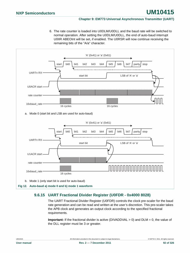
NXP Semiconductors UM10415Chapter 9: EM773 Universal Asynchronous Transmitter (UART)
6. The rate counter is loaded into U0DLM/U0DLL and the baud rate will be switched to normal operation. After setting the U0DLM/U0DLL, the end of auto-baud interrupt U0IIR ABEOInt will be set, if enabled. The U0RSR will now continue receiving the remaining bits of the ”A/a" character.
9.6.15 UART Fractional Divider Register (U0FDR - 0x4000 8028)
The UART Fractional Divider Register (U0FDR) controls the clock pre-scaler for the baud rate generation and can be read and written at the user’s discretion. This pre-scaler takes the APB clock and generates an output clock according to the specified fractional requirements.
Important: If the fractional divider is active (DIVADDVAL > 0) and DLM = 0, the value of the DLL register must be 3 or greater.
a. Mode 0 (start bit and LSB are used for auto-baud)
b. Mode 1 (only start bit is used for auto-baud)
Fig 12. Auto-baud a) mode 0 and b) mode 1 waveform
UARTn RXstart bit LSB of 'A' or 'a'
U0ACR start
rate counter
start bit0 bit1 bit2 bit3 bit4 bit5 bit6 bit7 parity stop
'A' (0x41) or 'a' (0x61)
16 cycles 16 cycles16xbaud_rate
UARTn RXstart bit LSB of 'A' or 'a'
rate counter
'A' (0x41) or 'a' (0x61)
start bit0 bit1 bit2 bit3 bit4 bit5 bit6 bit7 parity stop
U1ACR start
16 cycles16xbaud_rate
UM10415 All information provided in this document is subject to legal disclaimers. © NXP B.V. 2011. All rights reserved.
User manual Rev. 2 — 7 December 2011 92 of 326
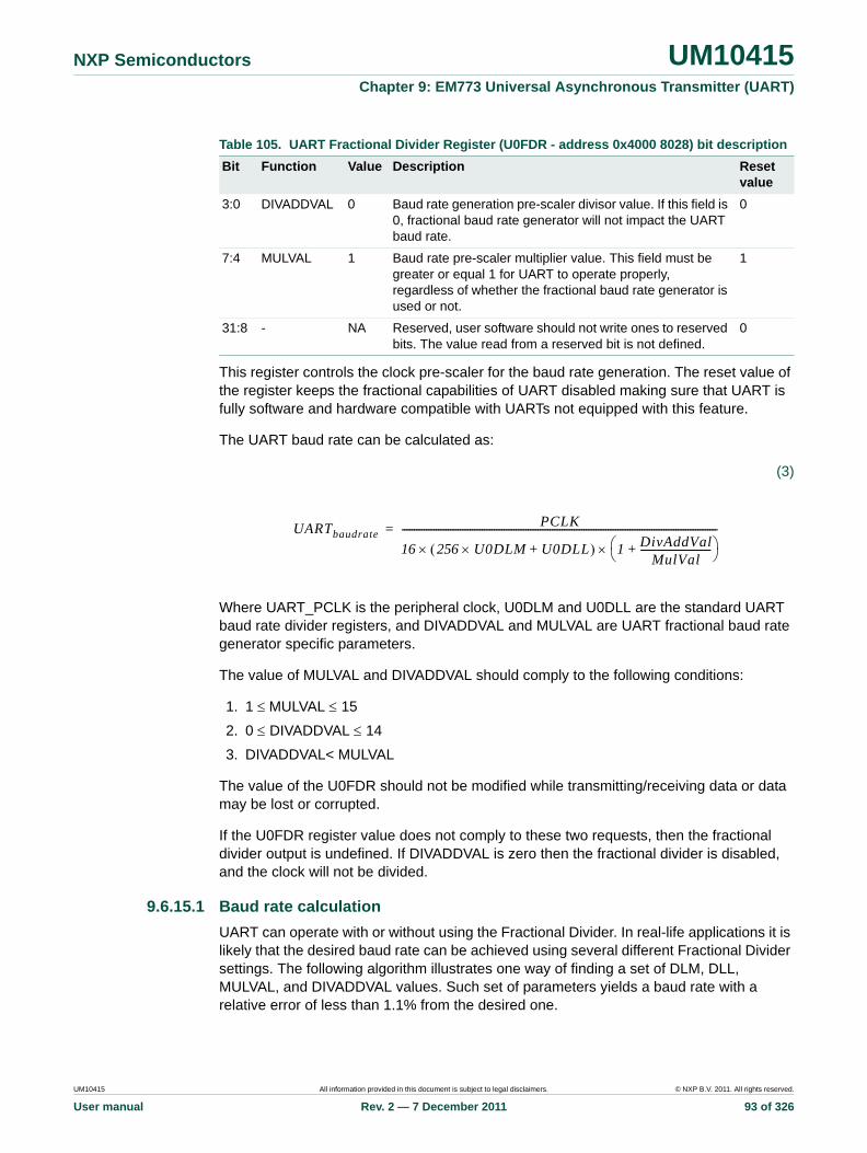
NXP Semiconductors UM10415Chapter 9: EM773 Universal Asynchronous Transmitter (UART)
This register controls the clock pre-scaler for the baud rate generation. The reset value of the register keeps the fractional capabilities of UART disabled making sure that UART is fully software and hardware compatible with UARTs not equipped with this feature.
The UART baud rate can be calculated as:
(3)
Where UART_PCLK is the peripheral clock, U0DLM and U0DLL are the standard UART baud rate divider registers, and DIVADDVAL and MULVAL are UART fractional baud rate generator specific parameters.
The value of MULVAL and DIVADDVAL should comply to the following conditions:
1. 1 MULVAL 15
2. 0 DIVADDVAL 14
3. DIVADDVAL< MULVAL
The value of the U0FDR should not be modified while transmitting/receiving data or data may be lost or corrupted.
If the U0FDR register value does not comply to these two requests, then the fractional divider output is undefined. If DIVADDVAL is zero then the fractional divider is disabled, and the clock will not be divided.
9.6.15.1 Baud rate calculation
UART can operate with or without using the Fractional Divider. In real-life applications it is likely that the desired baud rate can be achieved using several different Fractional Divider settings. The following algorithm illustrates one way of finding a set of DLM, DLL, MULVAL, and DIVADDVAL values. Such set of parameters yields a baud rate with a relative error of less than 1.1% from the desired one.
Table 105. UART Fractional Divider Register (U0FDR - address 0x4000 8028) bit description
Bit Function Value Description Reset value
3:0 DIVADDVAL 0 Baud rate generation pre-scaler divisor value. If this field is 0, fractional baud rate generator will not impact the UART baud rate.
0
7:4 MULVAL 1 Baud rate pre-scaler multiplier value. This field must be greater or equal 1 for UART to operate properly, regardless of whether the fractional baud rate generator is used or not.
1
31:8 - NA Reserved, user software should not write ones to reserved bits. The value read from a reserved bit is not defined.
0
UARTbaudratePCLK
16 256 U0DLM U0DLL+ 1 DivAddValMulVal
-----------------------------+
----------------------------------------------------------------------------------------------------------------------------------=
UM10415 All information provided in this document is subject to legal disclaimers. © NXP B.V. 2011. All rights reserved.
User manual Rev. 2 — 7 December 2011 93 of 326
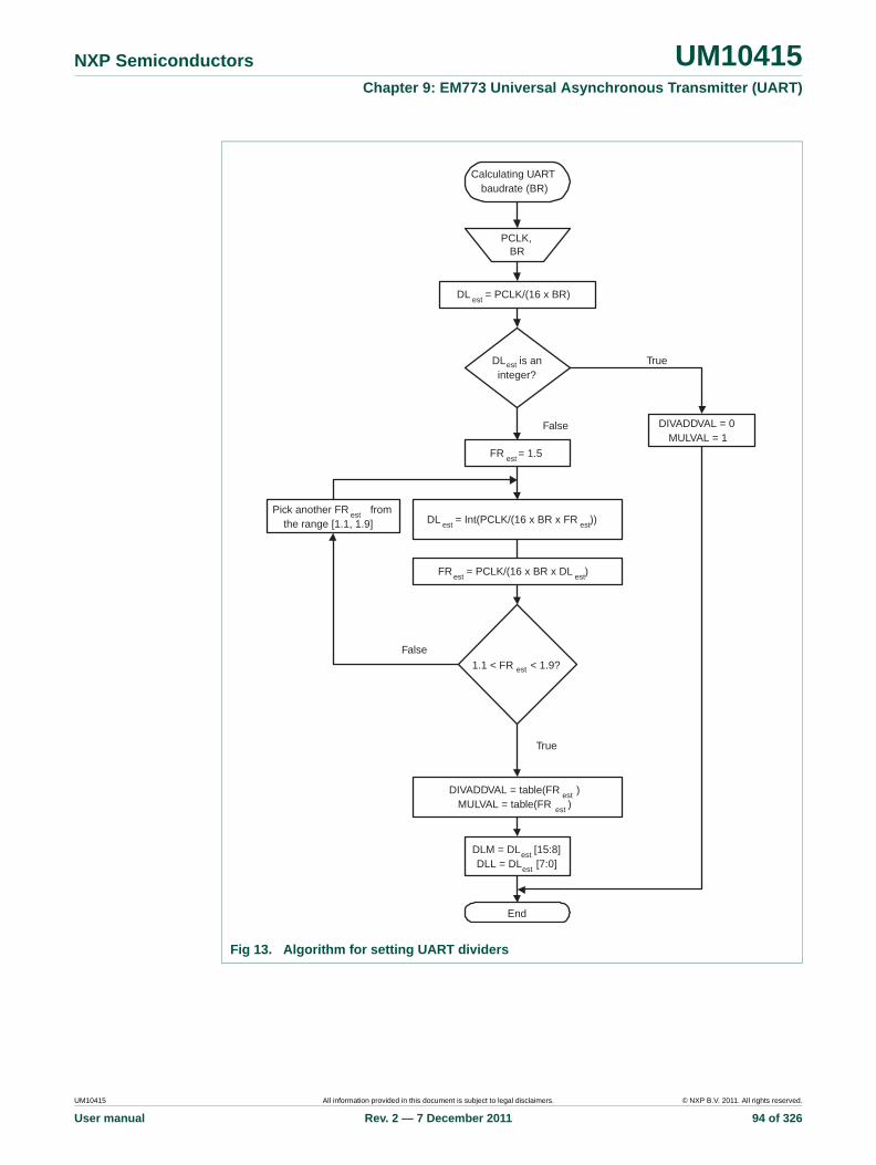
NXP Semiconductors UM10415Chapter 9: EM773 Universal Asynchronous Transmitter (UART)
Fig 13. Algorithm for setting UART dividers
PCLK,BR
Calculating UARTbaudrate (BR)
DL est = PCLK/(16 x BR)
DLest is aninteger?
DIVADDVAL = 0MULVAL = 1
True
FR est = 1.5
DL est = Int(PCLK/(16 x BR x FR est))
1.1 < FR est < 1.9?
Pick another FR est fromthe range [1.1, 1.9]
FRest = PCLK/(16 x BR x DL est)
DIVADDVAL = table(FR est )MULVAL = table(FR est )
DLM = DLest [15:8]DLL = DLest [7:0]
End
False
True
False
UM10415 All information provided in this document is subject to legal disclaimers. © NXP B.V. 2011. All rights reserved.
User manual Rev. 2 — 7 December 2011 94 of 326
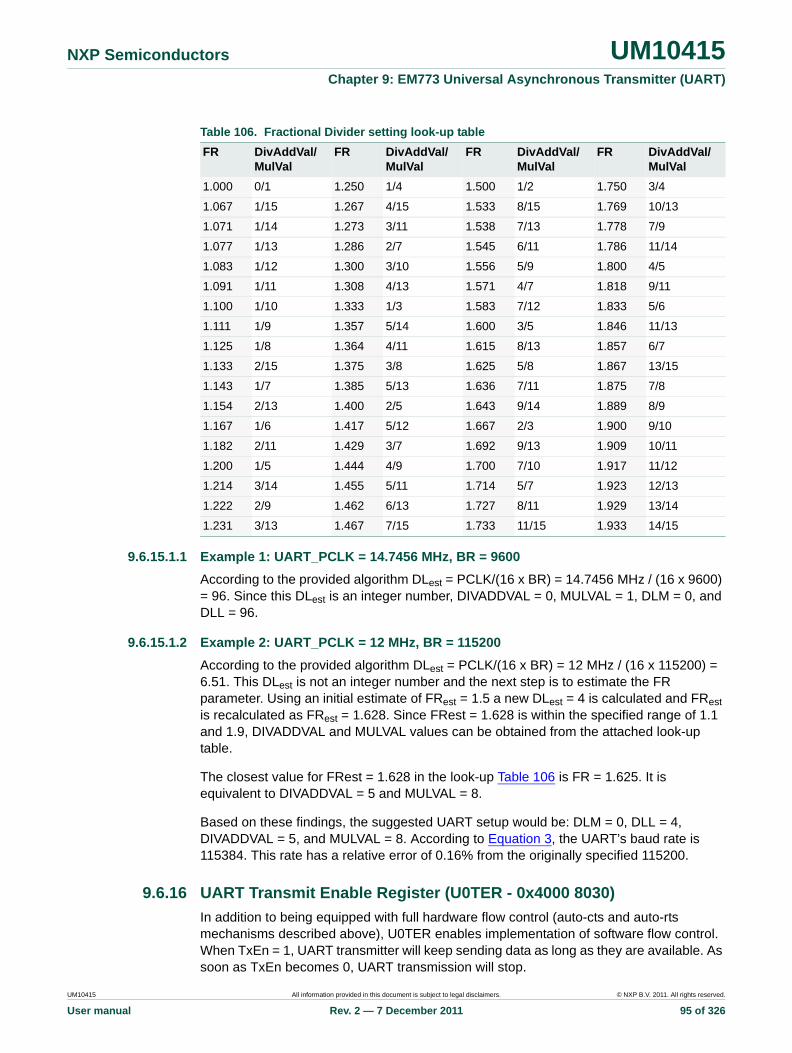
NXP Semiconductors UM10415Chapter 9: EM773 Universal Asynchronous Transmitter (UART)
9.6.15.1.1 Example 1: UART_PCLK = 14.7456 MHz, BR = 9600
According to the provided algorithm DLest = PCLK/(16 x BR) = 14.7456 MHz / (16 x 9600) = 96. Since this DLest is an integer number, DIVADDVAL = 0, MULVAL = 1, DLM = 0, and DLL = 96.
9.6.15.1.2 Example 2: UART_PCLK = 12 MHz, BR = 115200
According to the provided algorithm DLest = PCLK/(16 x BR) = 12 MHz / (16 x 115200) = 6.51. This DLest is not an integer number and the next step is to estimate the FR parameter. Using an initial estimate of FRest = 1.5 a new DLest = 4 is calculated and FRest is recalculated as FRest = 1.628. Since FRest = 1.628 is within the specified range of 1.1 and 1.9, DIVADDVAL and MULVAL values can be obtained from the attached look-up table.
The closest value for FRest = 1.628 in the look-up Table 106 is FR = 1.625. It is equivalent to DIVADDVAL = 5 and MULVAL = 8.
Based on these findings, the suggested UART setup would be: DLM = 0, DLL = 4, DIVADDVAL = 5, and MULVAL = 8. According to Equation 3, the UART’s baud rate is 115384. This rate has a relative error of 0.16% from the originally specified 115200.
9.6.16 UART Transmit Enable Register (U0TER - 0x4000 8030)
In addition to being equipped with full hardware flow control (auto-cts and auto-rts mechanisms described above), U0TER enables implementation of software flow control. When TxEn = 1, UART transmitter will keep sending data as long as they are available. As soon as TxEn becomes 0, UART transmission will stop.
Table 106. Fractional Divider setting look-up table
FR DivAddVal/MulVal
FR DivAddVal/MulVal
FR DivAddVal/MulVal
FR DivAddVal/MulVal
1.000 0/1 1.250 1/4 1.500 1/2 1.750 3/4
1.067 1/15 1.267 4/15 1.533 8/15 1.769 10/13
1.071 1/14 1.273 3/11 1.538 7/13 1.778 7/9
1.077 1/13 1.286 2/7 1.545 6/11 1.786 11/14
1.083 1/12 1.300 3/10 1.556 5/9 1.800 4/5
1.091 1/11 1.308 4/13 1.571 4/7 1.818 9/11
1.100 1/10 1.333 1/3 1.583 7/12 1.833 5/6
1.111 1/9 1.357 5/14 1.600 3/5 1.846 11/13
1.125 1/8 1.364 4/11 1.615 8/13 1.857 6/7
1.133 2/15 1.375 3/8 1.625 5/8 1.867 13/15
1.143 1/7 1.385 5/13 1.636 7/11 1.875 7/8
1.154 2/13 1.400 2/5 1.643 9/14 1.889 8/9
1.167 1/6 1.417 5/12 1.667 2/3 1.900 9/10
1.182 2/11 1.429 3/7 1.692 9/13 1.909 10/11
1.200 1/5 1.444 4/9 1.700 7/10 1.917 11/12
1.214 3/14 1.455 5/11 1.714 5/7 1.923 12/13
1.222 2/9 1.462 6/13 1.727 8/11 1.929 13/14
1.231 3/13 1.467 7/15 1.733 11/15 1.933 14/15
UM10415 All information provided in this document is subject to legal disclaimers. © NXP B.V. 2011. All rights reserved.
User manual Rev. 2 — 7 December 2011 95 of 326

NXP Semiconductors UM10415Chapter 9: EM773 Universal Asynchronous Transmitter (UART)
Although Table 107 describes how to use TxEn bit in order to achieve hardware flow control, it is strongly suggested to let UART hardware implemented auto flow control features take care of this, and limit the scope of TxEn to software flow control.
Table 107 describes how to use TXEn bit in order to achieve software flow control.
9.6.17 UART RS485 Control register (U0RS485CTRL - 0x4000 804C)
The U0RS485CTRL register controls the configuration of the UART in RS-485/EIA-485 mode.
Table 107. UART Transmit Enable Register (U0TER - address 0x4000 8030) bit description
Bit Symbol Description Reset Value
6:0 - Reserved, user software should not write ones to reserved bits. The value read from a reserved bit is not defined.
NA
7 TXEN When this bit is 1, as it is after a Reset, data written to the THR is output on the TXD pin as soon as any preceding data has been sent. If this bit cleared to 0 while a character is being sent, the transmission of that character is completed, but no further characters are sent until this bit is set again. In other words, a 0 in this bit blocks the transfer of characters from the THR or TX FIFO into the transmit shift register. Software can clear this bit when it detects that the a hardware-handshaking TX-permit signal (CTS) has gone false, or with software handshaking, when it receives an XOFF character (DC3). Software can set this bit again when it detects that the TX-permit signal has gone true, or when it receives an XON (DC1) character.
1
31:8 - Reserved -
Table 108. UART RS485 Control register (U0RS485CTRL - address 0x4000 804C) bit description
Bit Symbol Value Description Reset value
0 NMMEN 0 RS-485/EIA-485 Normal Multidrop Mode (NMM) is disabled.
0
1 RS-485/EIA-485 Normal Multidrop Mode (NMM) is enabled. In this mode, an address is detected when a received byte causes the UART to set the parity error and generate an interrupt.
1 RXDIS 0 The receiver is enabled. 0
1 The receiver is disabled.
2 AADEN 0 Auto Address Detect (AAD) is disabled. 0
1 Auto Address Detect (AAD) is enabled.
3 SEL 0 If direction control is enabled (bit DCTRL = 1), pin RTS is used for direction control.
0
1 If direction control is enabled (bit DCTRL = 1), pin DTR is used for direction control.
4 DCTRL 0 Disable Auto Direction Control. 0
1 Enable Auto Direction Control.
5 OINV This bit reverses the polarity of the direction control signal on the RTS (or DTR) pin.
0
UM10415 All information provided in this document is subject to legal disclaimers. © NXP B.V. 2011. All rights reserved.
User manual Rev. 2 — 7 December 2011 96 of 326

NXP Semiconductors UM10415Chapter 9: EM773 Universal Asynchronous Transmitter (UART)
9.6.18 UART RS-485 Address Match register (U0RS485ADRMATCH - 0x4000 8050)
The U0RS485ADRMATCH register contains the address match value for RS-485/EIA-485 mode.
9.6.19 UART1 RS-485 Delay value register (U0RS485DLY - 0x4000 8054)
The user may program the 8-bit RS485DLY register with a delay between the last stop bit leaving the TXFIFO and the de-assertion of RTS (or DTR). This delay time is in periods of the baud clock. Any delay time from 0 to 255 bit times may be programmed.
9.6.20 RS-485/EIA-485 modes of operation
The RS-485/EIA-485 feature allows the UART to be configured as an addressable slave. The addressable slave is one of multiple slaves controlled by a single master.
The UART master transmitter will identify an address character by setting the parity (9th) bit to ‘1’. For data characters, the parity bit is set to ‘0’.
Each UART slave receiver can be assigned a unique address. The slave can be programmed to either manually or automatically reject data following an address which is not theirs.
0 The direction control pin will be driven to logic ‘0’ when the transmitter has data to be sent. It will be driven to logic ‘1’ after the last bit of data has been transmitted.
1 The direction control pin will be driven to logic ‘1’ when the transmitter has data to be sent. It will be driven to logic ‘0’ after the last bit of data has been transmitted.
31:6 - - Reserved, user software should not write ones to reserved bits. The value read from a reserved bit is not defined.
NA
Table 108. UART RS485 Control register (U0RS485CTRL - address 0x4000 804C) bit description …continued
Bit Symbol Value Description Reset value
Table 109. UART RS-485 Address Match register (U0RS485ADRMATCH - address 0x4000 8050) bit description
Bit Symbol Description Reset value
7:0 ADRMATCH Contains the address match value. 0x00
31:8 - Reserved -
Table 110. UART RS-485 Delay value register (U0RS485DLY - address 0x4000 8054) bit description
Bit Symbol Description Reset value
7:0 DLY Contains the direction control (RTS or DTR) delay value. This register works in conjunction with an 8-bit counter.
0x00
31:8 - Reserved, user software should not write ones to reserved bits. The value read from a reserved bit is not defined.
NA
UM10415 All information provided in this document is subject to legal disclaimers. © NXP B.V. 2011. All rights reserved.
User manual Rev. 2 — 7 December 2011 97 of 326
NXP Semiconductors UM10415Chapter 9: EM773 Universal Asynchronous Transmitter (UART)
RS-485/EIA-485 Normal Multidrop Mode (NMM)
Setting the RS485CTRL bit 0 enables this mode. In this mode, an address is detected when a received byte causes the UART to set the parity error and generate an interrupt.
If the receiver is disabled (RS485CTRL bit 1 = ‘1’), any received data bytes will be ignored and will not be stored in the RXFIFO. When an address byte is detected (parity bit = ‘1’) it will be placed into the RXFIFO and an Rx Data Ready Interrupt will be generated. The processor can then read the address byte and decide whether or not to enable the receiver to accept the following data.
While the receiver is enabled (RS485CTRL bit 1 =’0’), all received bytes will be accepted and stored in the RXFIFO regardless of whether they are data or address. When an address character is received a parity error interrupt will be generated and the processor can decide whether or not to disable the receiver.
RS-485/EIA-485 Auto Address Detection (AAD) mode
When both RS485CTRL register bits 0 (9-bit mode enable) and 2 (AAD mode enable) are set, the UART is in auto address detect mode.
In this mode, the receiver will compare any address byte received (parity = ‘1’) to the 8-bit value programmed into the RS485ADRMATCH register.
If the receiver is disabled (RS485CTRL bit 1 = ‘1’), any received byte will be discarded if it is either a data byte OR an address byte which fails to match the RS485ADRMATCH value.
When a matching address character is detected it will be pushed onto the RXFIFO along with the parity bit, and the receiver will be automatically enabled (RS485CTRL bit 1 will be cleared by hardware). The receiver will also generate an Rx Data Ready Interrupt.
While the receiver is enabled (RS485CTRL bit 1 = ‘0’), all bytes received will be accepted and stored in the RXFIFO until an address byte which does not match the RS485ADRMATCH value is received. When this occurs, the receiver will be automatically disabled in hardware (RS485CTRL bit 1 will be set), The received non-matching address character will not be stored in the RXFIFO.
RS-485/EIA-485 Auto Direction Control
RS485/EIA-485 mode includes the option of allowing the transmitter to automatically control the state of the DIR pin as a direction control output signal.
Setting RS485CTRL bit 4 = ‘1’ enables this feature.
Direction control, if enabled, will use the RTS pin when RS485CTRL bit 3 = ‘0’. It will use the DTR pin when RS485CTRL bit 3 = ‘1’.
When Auto Direction Control is enabled, the selected pin will be asserted (driven LOW) when the CPU writes data into the TXFIFO. The pin will be de-asserted (driven HIGH) once the last bit of data has been transmitted. See bits 4 and 5 in the RS485CTRL register.
The RS485CTRL bit 4 takes precedence over all other mechanisms controlling the direction control pin with the exception of loopback mode.
RS485/EIA-485 driver delay time
UM10415 All information provided in this document is subject to legal disclaimers. © NXP B.V. 2011. All rights reserved.
User manual Rev. 2 — 7 December 2011 98 of 326

NXP Semiconductors UM10415Chapter 9: EM773 Universal Asynchronous Transmitter (UART)
The driver delay time is the delay between the last stop bit leaving the TXFIFO and the de-assertion of RTS. This delay time can be programmed in the 8-bit RS485DLY register. The delay time is in periods of the baud clock. Any delay time from 0 to 255 bit times may be used.
RS485/EIA-485 output inversion
The polarity of the direction control signal on the RTS (or DTR) pins can be reversed by programming bit 5 in the U0RS485CTRL register. When this bit is set, the direction control pin will be driven to logic 1 when the transmitter has data waiting to be sent. The direction control pin will be driven to logic 0 after the last bit of data has been transmitted.
9.7 Architecture
The architecture of the UART is shown below in the block diagram.
The APB interface provides a communications link between the CPU or host and the UART.
The UART receiver block, U0RX, monitors the serial input line, RXD, for valid input. The UART RX Shift Register (U0RSR) accepts valid characters via RXD. After a valid character is assembled in the U0RSR, it is passed to the UART RX Buffer Register FIFO to await access by the CPU or host via the generic host interface.
The UART transmitter block, U0TX, accepts data written by the CPU or host and buffers the data in the UART TX Holding Register FIFO (U0THR). The UART TX Shift Register (U0TSR) reads the data stored in the U0THR and assembles the data to transmit via the serial output pin, TXD1.
The UART Baud Rate Generator block, U0BRG, generates the timing enables used by the UART TX block. The U0BRG clock input source is UART_PCLK. The main clock is divided down per the divisor specified in the U0DLL and U0DLM registers. This divided down clock is a 16x oversample clock, NBAUDOUT.
The interrupt interface contains registers U0IER and U0IIR. The interrupt interface receives several one clock wide enables from the U0TX and U0RX blocks.
Status information from the U0TX and U0RX is stored in the U0LSR. Control information for the U0TX and U0RX is stored in the U0LCR.
UM10415 All information provided in this document is subject to legal disclaimers. © NXP B.V. 2011. All rights reserved.
User manual Rev. 2 — 7 December 2011 99 of 326
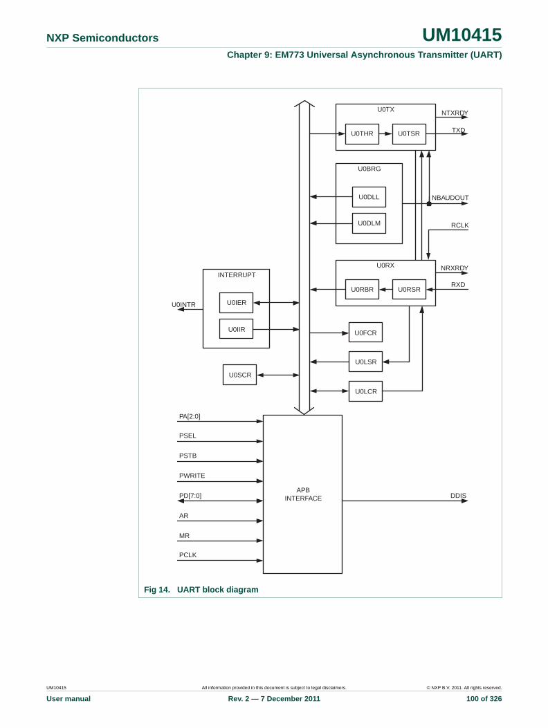
NXP Semiconductors UM10415Chapter 9: EM773 Universal Asynchronous Transmitter (UART)
Fig 14. UART block diagram
APBINTERFACE
U0LCR
U0RX
DDIS
U0LSR
U0FCR
U0BRG
U0TX
INTERRUPT
PA[2:0]
PSEL
PSTB
PWRITE
PD[7:0]
AR
MR
PCLK
U0INTR
U0SCR
NTXRDY
TXD
NBAUDOUT
RCLK
NRXRDY
RXDU0RBR U0RSR
U0DLM
U0DLL
U0THR U0TSR
U0IIR
U0IER
UM10415 All information provided in this document is subject to legal disclaimers. © NXP B.V. 2011. All rights reserved.
User manual Rev. 2 — 7 December 2011 100 of 326

10.1 How to read this chapter
The I2C-bus block is identical for all EM773 parts.
10.2 Basic configuration
The I2C-bus interface is configured using the following registers:
1. Pins: The I2C pin functions and the I2C mode are configured in the IOCONFIG register block (Section 6.4.1, Table 55 and Table 56).
2. Power and peripheral clock: In the SYSAHBCLKCTRL register, set bit 5 (Table 17).
3. Reset: Before accessing the I2C block, ensure that the I2C_RST_N bit (bit 1) in the PRESETCTRL register (Table 5) is set to 1. This de-asserts the reset signal to the I2C block.
10.3 Features
• Standard I2C-compliant bus interfaces may be configured as Master, Slave, or Master/Slave.
• Arbitration is handled between simultaneously transmitting masters without corruption of serial data on the bus.
• Programmable clock allows adjustment of I2C transfer rates.
• Data transfer is bidirectional between masters and slaves.
• Serial clock synchronization allows devices with different bit rates to communicate via one serial bus.
• Serial clock synchronization is used as a handshake mechanism to suspend and resume serial transfer.
• Supports Fast-mode Plus.
• Optional recognition of up to four distinct slave addresses.
• Monitor mode allows observing all I2C-bus traffic, regardless of slave address.
• I2C-bus can be used for test and diagnostic purposes.
• The I2C-bus contains a standard I2C-compliant bus interface with two pins.
10.4 Applications
Interfaces to external I2C standard parts, such as serial RAMs, LCDs, tone generators, other microcontrollers, etc.
10.5 General description
A typical I2C-bus configuration is shown in Figure 15. Depending on the state of the direction bit (R/W), two types of data transfers are possible on the I2C-bus:
UM10415Chapter 10: EM773 I2C-bus interfaceRev. 2 — 7 December 2011 User manual
UM10415 All information provided in this document is subject to legal disclaimers. © NXP B.V. 2011. All rights reserved.
User manual Rev. 2 — 7 December 2011 101 of 326

NXP Semiconductors UM10415Chapter 10: EM773 I2C-bus interface
• Data transfer from a master transmitter to a slave receiver. The first byte transmitted by the master is the slave address. Next follows a number of data bytes. The slave returns an acknowledge bit after each received byte.
• Data transfer from a slave transmitter to a master receiver. The first byte (the slave address) is transmitted by the master. The slave then returns an acknowledge bit. Next follows the data bytes transmitted by the slave to the master. The master returns an acknowledge bit after all received bytes other than the last byte. At the end of the last received byte, a “not acknowledge” is returned. The master device generates all of the serial clock pulses and the START and STOP conditions. A transfer is ended with a STOP condition or with a Repeated START condition. Since a Repeated START condition is also the beginning of the next serial transfer, the I2C bus will not be released.
The I2C interface is byte oriented and has four operating modes: master transmitter mode, master receiver mode, slave transmitter mode and slave receiver mode.
The I2C interface complies with the entire I2C specification, supporting the ability to turn power off to the ARM Cortex-M0 without interfering with other devices on the same I2C-bus.
10.5.1 I2C Fast-mode Plus
Fast-Mode Plus supports a 1 Mbit/sec transfer rate to communicate with the I2C-bus products which NXP Semiconductors is now providing.
Fig 15. I2C-bus configuration
OTHER DEVICE WITHI 2C INTERFACE
pull-upresistor
OTHER DEVICE WITHI 2C INTERFACE
EM773
SDA SCL
I 2C bus
SCL
SDA
pull-upresistor
UM10415 All information provided in this document is subject to legal disclaimers. © NXP B.V. 2011. All rights reserved.
User manual Rev. 2 — 7 December 2011 102 of 326
NXP Semiconductors UM10415Chapter 10: EM773 I2C-bus interface
10.6 Pin description
The I2C-bus pins must be configured through the IOCON_PIO0_4 (Table 55) and IOCON_PIO0_5 (Table 56) registers for Standard/ Fast-mode or Fast-mode Plus. In Fast-mode Plus, rates above 400 kHz and up to 1 MHz may be selected. The I2C-bus pins are open-drain outputs and fully compatible with the I2C-bus specification.
10.7 Clocking and power control
The clock to the I2C-bus interface (PCLK_I2C) is provided by the system clock (see Figure 3). This clock can be disabled through bit 5 in the AHBCLKCTRL register (Table 17) for power savings.
Remark: Before accessing the I2C block, ensure that the I2C_RST_N bit (bit 1) in the PRESETCTRL register (Table 5) is set to 1. This de-asserts the reset signal to the I2C block.
10.8 Register description
Table 111. I2C-bus pin description
Pin Type Description
SDA Input/Output I2C Serial Data
SCL Input/Output I2C Serial Clock
Table 112. Register overview: I2C (base address 0x4000 0000)
Name Access Address offset
Description Reset value[1]
I2C0CONSET R/W 0x000 I2C Control Set Register. When a one is written to a bit of this register, the corresponding bit in the I2C control register is set. Writing a zero has no effect on the corresponding bit in the I2C control register.
0x00
I2C0STAT RO 0x004 I2C Status Register. During I2C operation, this register provides detailed status codes that allow software to determine the next action needed.
0xF8
I2C0DAT R/W 0x008 I2C Data Register. During master or slave transmit mode, data to be transmitted is written to this register. During master or slave receive mode, data that has been received may be read from this register.
0x00
I2C0ADR0 R/W 0x00C I2C Slave Address Register 0. Contains the 7-bit slave address for operation of the I2C interface in slave mode, and is not used in master mode. The least significant bit determines whether a slave responds to the General Call address.
0x00
I2C0SCLH R/W 0x010 SCH Duty Cycle Register High Half Word. Determines the high time of the I2C clock.
0x04
I2C0SCLL R/W 0x014 SCL Duty Cycle Register Low Half Word. Determines the low time of the I2C clock. I2nSCLL and I2nSCLH together determine the clock frequency generated by an I2C master and certain times used in slave mode.
0x04
I2C0CONCLR WO 0x018 I2C Control Clear Register. When a one is written to a bit of this register, the corresponding bit in the I2C control register is cleared. Writing a zero has no effect on the corresponding bit in the I2C control register.
NA
I2C0MMCTRL R/W 0x01C Monitor mode control register. 0x00
UM10415 All information provided in this document is subject to legal disclaimers. © NXP B.V. 2011. All rights reserved.
User manual Rev. 2 — 7 December 2011 103 of 326

NXP Semiconductors UM10415Chapter 10: EM773 I2C-bus interface
[1] Reset value reflects the data stored in used bits only. It does not include reserved bits content.
10.8.1 I2C Control Set register (I2C0CONSET - 0x4000 0000)
The I2CONSET registers control setting of bits in the I2CON register that controls operation of the I2C interface. Writing a one to a bit of this register causes the corresponding bit in the I2C control register to be set. Writing a zero has no effect.
I2C0ADR1 R/W 0x020 I2C Slave Address Register 1. Contains the 7-bit slave address for operation of the I2C interface in slave mode, and is not used in master mode. The least significant bit determines whether a slave responds to the General Call address.
0x00
I2C0ADR2 R/W 0x024 I2C Slave Address Register 2. Contains the 7-bit slave address for operation of the I2C interface in slave mode, and is not used in master mode. The least significant bit determines whether a slave responds to the General Call address.
0x00
I2C0ADR3 R/W 0x028 I2C Slave Address Register 3. Contains the 7-bit slave address for operation of the I2C interface in slave mode, and is not used in master mode. The least significant bit determines whether a slave responds to the General Call address.
0x00
I2C0DATA_ BUFFER
RO 0x02C Data buffer register. The contents of the 8 MSBs of the I2DAT shift register will be transferred to the DATA_BUFFER automatically after every nine bits (8 bits of data plus ACK or NACK) has been received on the bus.
0x00
I2C0MASK0 R/W 0x030 I2C Slave address mask register 0. This mask register is associated with I2ADR0 to determine an address match. The mask register has no effect when comparing to the General Call address (‘0000000’).
0x00
I2C0MASK1 R/W 0x034 I2C Slave address mask register 1. This mask register is associated with I2ADR0 to determine an address match. The mask register has no effect when comparing to the General Call address (‘0000000’).
0x00
I2C0MASK2 R/W 0x038 I2C Slave address mask register 2. This mask register is associated with I2ADR0 to determine an address match. The mask register has no effect when comparing to the General Call address (‘0000000’).
0x00
I2C0MASK3 R/W 0x03C I2C Slave address mask register 3. This mask register is associated with I2ADR0 to determine an address match. The mask register has no effect when comparing to the General Call address (‘0000000’).
0x00
Table 112. Register overview: I2C (base address 0x4000 0000) …continued
Name Access Address offset
Description Reset value[1]
Table 113. I2C Control Set register (I2C0CONSET - address 0x4000 0000) bit description
Bit Symbol Description Reset value
1:0 - Reserved. User software should not write ones to reserved bits. The value read from a reserved bit is not defined.
NA
2 AA Assert acknowledge flag.
3 SI I2C interrupt flag. 0
4 STO STOP flag. 0
5 STA START flag. 0
6 I2EN I2C interface enable. 0
31:7 - Reserved. The value read from a reserved bit is not defined. -
UM10415 All information provided in this document is subject to legal disclaimers. © NXP B.V. 2011. All rights reserved.
User manual Rev. 2 — 7 December 2011 104 of 326

NXP Semiconductors UM10415Chapter 10: EM773 I2C-bus interface
I2EN I2C Interface Enable. When I2EN is 1, the I2C interface is enabled. I2EN can be cleared by writing 1 to the I2ENC bit in the I2CONCLR register. When I2EN is 0, the I2C interface is disabled.
When I2EN is “0”, the SDA and SCL input signals are ignored, the I2C block is in the “not addressed” slave state, and the STO bit is forced to “0”.
I2EN should not be used to temporarily release the I2C-bus since, when I2EN is reset, the I2C-bus status is lost. The AA flag should be used instead.
STA is the START flag. Setting this bit causes the I2C interface to enter master mode and transmit a START condition or transmit a Repeated START condition if it is already in master mode.
When STA is 1 and the I2C interface is not already in master mode, it enters master mode, checks the bus and generates a START condition if the bus is free. If the bus is not free, it waits for a STOP condition (which will free the bus) and generates a START condition after a delay of a half clock period of the internal clock generator. If the I2C interface is already in master mode and data has been transmitted or received, it transmits a Repeated START condition. STA may be set at any time, including when the I2C interface is in an addressed slave mode.
STA can be cleared by writing 1 to the STAC bit in the I2CONCLR register. When STA is 0, no START condition or Repeated START condition will be generated.
If STA and STO are both set, then a STOP condition is transmitted on the I2C-bus if it the interface is in master mode, and transmits a START condition thereafter. If the I2C interface is in slave mode, an internal STOP condition is generated, but is not transmitted on the bus.
STO is the STOP flag. Setting this bit causes the I2C interface to transmit a STOP condition in master mode, or recover from an error condition in slave mode. When STO is 1 in master mode, a STOP condition is transmitted on the I2C-bus. When the bus detects the STOP condition, STO is cleared automatically.
In slave mode, setting this bit can recover from an error condition. In this case, no STOP condition is transmitted to the bus. The hardware behaves as if a STOP condition has been received and it switches to “not addressed” slave receiver mode. The STO flag is cleared by hardware automatically.
SI is the I2C Interrupt Flag. This bit is set when the I2C state changes. However, entering state F8 does not set SI since there is nothing for an interrupt service routine to do in that case.
While SI is set, the low period of the serial clock on the SCL line is stretched, and the serial transfer is suspended. When SCL is HIGH, it is unaffected by the state of the SI flag. SI must be reset by software, by writing a 1 to the SIC bit in I2CONCLR register.
AA is the Assert Acknowledge Flag. When set to 1, an acknowledge (low level to SDA) will be returned during the acknowledge clock pulse on the SCL line on the following situations:
1. The address in the Slave Address Register has been received.
UM10415 All information provided in this document is subject to legal disclaimers. © NXP B.V. 2011. All rights reserved.
User manual Rev. 2 — 7 December 2011 105 of 326
NXP Semiconductors UM10415Chapter 10: EM773 I2C-bus interface
2. The General Call address has been received while the General Call bit (GC) in I2ADR is set.
3. A data byte has been received while the I2C is in the master receiver mode.
4. A data byte has been received while the I2C is in the addressed slave receiver mode
The AA bit can be cleared by writing 1 to the AAC bit in the I2CONCLR register. When AA is 0, a not acknowledge (HIGH level to SDA) will be returned during the acknowledge clock pulse on the SCL line on the following situations:
1. A data byte has been received while the I2C is in the master receiver mode.
2. A data byte has been received while the I2C is in the addressed slave receiver mode.
10.8.2 I2C Status register (I2C0STAT - 0x4000 0004)
Each I2C Status register reflects the condition of the corresponding I2C interface. The I2C Status register is Read-Only.
The three least significant bits are always 0. Taken as a byte, the status register contents represent a status code. There are 26 possible status codes. When the status code is 0xF8, there is no relevant information available and the SI bit is not set. All other 25 status codes correspond to defined I2C states. When any of these states entered, the SI bit will be set. For a complete list of status codes, refer to tables from Table 129 to Table 134.
10.8.3 I2C Data register (I2C0DAT - 0x4000 0008)
This register contains the data to be transmitted or the data just received. The CPU can read and write to this register only while it is not in the process of shifting a byte, when the SI bit is set. Data in I2DAT remains stable as long as the SI bit is set. Data in I2DAT is always shifted from right to left: the first bit to be transmitted is the MSB (bit 7), and after a byte has been received, the first bit of received data is located at the MSB of I2DAT.
10.8.4 I2C Slave Address register 0 (I2C0ADR0- 0x4000 000C)
This register is readable and writable and are only used when an I2C interface is set to slave mode. In master mode, this register has no effect. The LSB of I2ADR is the General Call bit. When this bit is set, the General Call address (0x00) is recognized.
Table 114. I2C Status register (I2C0STAT - 0x4000 0004) bit description
Bit Symbol Description Reset value
2:0 - These bits are unused and are always 0. 0
7:3 Status These bits give the actual status information about the I2C interface.
0x1F
31:8 - Reserved. The value read from a reserved bit is not defined. -
Table 115. I2C Data register (I2C0DAT - 0x4000 0008) bit description
Bit Symbol Description Reset value
7:0 Data This register holds data values that have been received or are to be transmitted.
0
31:8 - Reserved. The value read from a reserved bit is not defined. -
UM10415 All information provided in this document is subject to legal disclaimers. © NXP B.V. 2011. All rights reserved.
User manual Rev. 2 — 7 December 2011 106 of 326
NXP Semiconductors UM10415Chapter 10: EM773 I2C-bus interface
Any of these registers which contain the bit 00x will be disabled and will not match any address on the bus. The slave address register will be cleared to this disabled state on reset. See also Table 122.
10.8.5 I2C SCL HIGH and LOW duty cycle registers (I2C0SCLH - 0x4000 0010 and I2C0SCLL- 0x4000 0014)
10.8.5.1 Selecting the appropriate I2C data rate and duty cycle
Software must set values for the registers I2SCLH and I2SCLL to select the appropriate data rate and duty cycle. I2SCLH defines the number of I2C_PCLK cycles for the SCL HIGH time, I2SCLL defines the number of I2C_PCLK cycles for the SCL low time. The frequency is determined by the following formula (I2C_PCLK is the frequency of the peripheral I2C clock):
(4)
The values for I2SCLL and I2SCLH must ensure that the data rate is in the appropriate I2C data rate range. Each register value must be greater than or equal to 4. Table 119 gives some examples of I2C-bus rates based on I2C_PCLK frequency and I2SCLL and I2SCLH values.
Table 116. I2C Slave Address register 0 (I2C0ADR0- 0x4000 000C) bit description
Bit Symbol Description Reset value
0 GC General Call enable bit. 0
7:1 Address The I2C device address for slave mode. 0x00
31:8 - Reserved. The value read from a reserved bit is not defined. -
Table 117. I2C SCL HIGH Duty Cycle register (I2C0SCLH - address 0x4000 0010) bit description
Bit Symbol Description Reset value
15:0 SCLH Count for SCL HIGH time period selection. 0x0004
31:16 - Reserved. The value read from a reserved bit is not defined. -
Table 118. I2C SCL Low duty cycle register (I2C0SCLL - 0x4000 0014) bit description
Bit Symbol Description Reset value
15:0 SCLL Count for SCL low time period selection. 0x0004
31:16 - Reserved. The value read from a reserved bit is not defined. -
I2CbitfrequencyI2CPCLK
I2CSCLH I2CSCLL+---------------------------------------------------------=
UM10415 All information provided in this document is subject to legal disclaimers. © NXP B.V. 2011. All rights reserved.
User manual Rev. 2 — 7 December 2011 107 of 326

NXP Semiconductors UM10415Chapter 10: EM773 I2C-bus interface
I2SCLL and I2SCLH values should not necessarily be the same. Software can set different duty cycles on SCL by setting these two registers. For example, the I2C-bus specification defines the SCL low time and high time at different values for a Fast-mode and Fast-mode Plus I2C.
10.8.6 I2C Control Clear register (I2C0CONCLR - 0x4000 0018)
The I2CONCLR registers control clearing of bits in the I2CON register that controls operation of the I2C interface. Writing a one to a bit of this register causes the corresponding bit in the I2C control register to be cleared. Writing a zero has no effect.
AAC is the Assert Acknowledge Clear bit. Writing a 1 to this bit clears the AA bit in the I2CONSET register. Writing 0 has no effect.
SIC is the I2C Interrupt Clear bit. Writing a 1 to this bit clears the SI bit in the I2CONSET register. Writing 0 has no effect.
STAC is the START flag Clear bit. Writing a 1 to this bit clears the STA bit in the I2CONSET register. Writing 0 has no effect.
I2ENC is the I2C Interface Disable bit. Writing a 1 to this bit clears the I2EN bit in the I2CONSET register. Writing 0 has no effect.
10.8.7 I2C Monitor mode control register (I2C0MMCTRL - 0x4000 001C)
This register controls the Monitor mode which allows the I2C module to monitor traffic on the I2C bus without actually participating in traffic or interfering with the I2C bus.
Table 119. I2SCLL + I2SCLH values for selected I2C clock values
I2C mode I2C bit frequency
I2C_PCLK (MHz)
6 8 10 12 16 20 30 40 50
I2SCLH + I2SCLL
Standard mode 100 kHz 60 80 100 120 160 200 300 400 500
Fast-mode 400 kHz 15 20 25 30 40 50 75 100 125
Fast-mode Plus 1 MHz - 8 10 12 16 20 30 40 50
Table 120. I2C Control Clear register (I2C0CONCLR - 0x4000 0018) bit description
Bit Symbol Description Reset value
1:0 - Reserved. User software should not write ones to reserved bits. The value read from a reserved bit is not defined.
NA
2 AAC Assert acknowledge Clear bit.
3 SIC I2C interrupt Clear bit. 0
4 - Reserved. User software should not write ones to reserved bits. The value read from a reserved bit is not defined.
NA
5 STAC START flag Clear bit. 0
6 I2ENC I2C interface Disable bit. 0
7 - Reserved. User software should not write ones to reserved bits. The value read from a reserved bit is not defined.
NA
31:8 - Reserved. The value read from a reserved bit is not defined. -
UM10415 All information provided in this document is subject to legal disclaimers. © NXP B.V. 2011. All rights reserved.
User manual Rev. 2 — 7 December 2011 108 of 326

NXP Semiconductors UM10415Chapter 10: EM773 I2C-bus interface
[1] When the ENA_SCL bit is cleared and the I2C no longer has the ability to stall the bus, interrupt response time becomes important. To give the part more time to respond to an I2C interrupt under these conditions, a DATA _BUFFER register is used (Section 10.8.9) to hold received data for a full 9-bit word transmission time.
Remark: The ENA_SCL and MATCH_ALL bits have no effect if the MM_ENA is ‘0’ (i.e. if the module is NOT in monitor mode).
10.8.7.1 Interrupt in Monitor mode
All interrupts will occur as normal when the module is in monitor mode. This means that the first interrupt will occur when an address-match is detected (any address received if the MATCH_ALL bit is set, otherwise an address matching one of the four address registers).
Subsequent to an address-match detection, interrupts will be generated after each data byte is received for a slave-write transfer, or after each byte that the module “thinks” it has transmitted for a slave-read transfer. In this second case, the data register will actually contain data transmitted by some other slave on the bus which was actually addressed by the master.
Table 121. I2C Monitor mode control register (I2C0MMCTRL - 0x4000 001C) bit description
Bit Symbol Value Description Reset value
0 MM_ENA Monitor mode enable. 0
0 Monitor mode disabled.
1 The I2C module will enter monitor mode. In this mode the SDA output will be forced high. This will prevent the I2C module from outputting data of any kind (including ACK) onto the I2C data bus.
Depending on the state of the ENA_SCL bit, the output may be also forced high, preventing the module from having control over the I2C clock line.
1 ENA_SCL SCL output enable. 0
0 When this bit is cleared to ‘0’, the SCL output will be forced high when the module is in monitor mode. As described above, this will prevent the module from having any control over the I2C clock line.
1 When this bit is set, the I2C module may exercise the same control over the clock line that it would in normal operation. This means that, acting as a slave peripheral, the I2C module can “stretch” the clock line (hold it low) until it has had time to respond to an I2C interrupt.[1]
2 MATCH_ALL Select interrupt register match. 0
0 When this bit is cleared, an interrupt will only be generated when a match occurs to one of the (up-to) four address registers described above. That is, the module will respond as a normal slave as far as address-recognition is concerned.
1 When this bit is set to ‘1’ and the I2C is in monitor mode, an interrupt will be generated on ANY address received. This will enable the part to monitor all traffic on the bus.
31:3 - - Reserved. The value read from reserved bits is not defined.
UM10415 All information provided in this document is subject to legal disclaimers. © NXP B.V. 2011. All rights reserved.
User manual Rev. 2 — 7 December 2011 109 of 326
NXP Semiconductors UM10415Chapter 10: EM773 I2C-bus interface
Following all of these interrupts, the processor may read the data register to see what was actually transmitted on the bus.
10.8.7.2 Loss of arbitration in Monitor mode
In monitor mode, the I2C module will not be able to respond to a request for information by the bus master or issue an ACK). Some other slave on the bus will respond instead. This will most probably result in a lost-arbitration state as far as our module is concerned.
Software should be aware of the fact that the module is in monitor mode and should not respond to any loss of arbitration state that is detected. In addition, hardware may be designed into the module to block some/all loss of arbitration states from occurring if those state would either prevent a desired interrupt from occurring or cause an unwanted interrupt to occur. Whether any such hardware will be added is still to be determined.
10.8.8 I2C Slave Address registers (I2C0ADR[1, 2, 3] - 0x4000 00[20, 24, 28])
These registers are readable and writable and are only used when an I2C interface is set to slave mode. In master mode, this register has no effect. The LSB of I2ADR is the General Call bit. When this bit is set, the General Call address (0x00) is recognized.
Any of these registers which contain the bit 00x will be disabled and will not match any address on the bus. All four registers will be cleared to this disabled state on reset.
10.8.9 I2C Data buffer register (I2C0DATA_BUFFER - 0x4000 002C)
In monitor mode, the I2C module may lose the ability to stretch the clock (stall the bus) if the ENA_SCL bit is not set. This means that the processor will have a limited amount of time to read the contents of the data received on the bus. If the processor reads the I2DAT shift register, as it ordinarily would, it could have only one bit-time to respond to the interrupt before the received data is overwritten by new data.
To give the processor more time to respond, a new 8-bit, read-only DATA_BUFFER register will be added. The contents of the 8 MSBs of the I2DAT shift register will be transferred to the DATA_BUFFER automatically after every nine bits (8 bits of data plus ACK or NACK) has been received on the bus. This means that the processor will have nine bit transmission times to respond to the interrupt and read the data before it is overwritten.
The processor will still have the ability to read I2DAT directly, as usual, and the behavior of I2DAT will not be altered in any way.
Although the DATA_BUFFER register is primarily intended for use in monitor mode with the ENA_SCL bit = ‘0’, it will be available for reading at any time under any mode of operation.
Table 122. I2C Slave Address registers (I2C0ADR[1, 2, 3]- 0x4000 00[20, 24, 28]) bit description
Bit Symbol Description Reset value
0 GC General Call enable bit. 0
7:1 Address The I2C device address for slave mode. 0x00
31:8 - Reserved. The value read from a reserved bit is not defined. 0
UM10415 All information provided in this document is subject to legal disclaimers. © NXP B.V. 2011. All rights reserved.
User manual Rev. 2 — 7 December 2011 110 of 326

NXP Semiconductors UM10415Chapter 10: EM773 I2C-bus interface
10.8.10 I2C Mask registers (I2C0MASK[0, 1, 2, 3] - 0x4000 00[30, 34, 38, 3C])
The four mask registers each contain seven active bits (7:1). Any bit in these registers which is set to ‘1’ will cause an automatic compare on the corresponding bit of the received address when it is compared to the I2ADDRn register associated with that mask register. In other words, bits in an I2ADDRn register which are masked are not taken into account in determining an address match.
On reset, all mask register bits are cleared to ‘0’.
The mask register has no effect on comparison to the General Call address (“0000000”).
Bits(31:8) and bit(0) of the mask registers are unused and should not be written to. These bits will always read back as zeros.
When an address-match interrupt occurs, the processor will have to read the data register (I2DAT) to determine what the received address was that actually caused the match.
10.9 I2C operating modes
In a given application, the I2C block may operate as a master, a slave, or both. In the slave mode, the I2C hardware looks for any one of its four slave addresses and the General Call address. If one of these addresses is detected, an interrupt is requested. If the processor wishes to become the bus master, the hardware waits until the bus is free before the master mode is entered so that a possible slave operation is not interrupted. If bus arbitration is lost in the master mode, the I2C block switches to the slave mode immediately and can detect its own slave address in the same serial transfer.
10.9.1 Master Transmitter mode
In this mode data is transmitted from master to slave. Before the master transmitter mode can be entered, the I2CONSET register must be initialized as shown in Table 125. I2EN must be set to 1 to enable the I2C function. If the AA bit is 0, the I2C interface will not acknowledge any address when another device is master of the bus, so it can not enter slave mode. The STA, STO and SI bits must be 0. The SI Bit is cleared by writing 1 to the SIC bit in the I2CONCLR register. THe STA bit should be cleared after writing the slave address.
Table 123. I2C Data buffer register (I2C0DATA_BUFFER - 0x4000 002C) bit description
Bit Symbol Description Reset value
7:0 Data This register holds contents of the 8 MSBs of the I2DAT shift register.
0
31:8 - Reserved. The value read from a reserved bit is not defined. 0
Table 124. I2C Mask registers (I2C0MASK[0, 1, 2, 3] - 0x4000 00[30, 34, 38, 3C]) bit description
Bit Symbol Description Reset value
0 - Reserved. User software should not write ones to reserved bits. This bit reads always back as 0.
0
7:1 MASK Mask bits. 0x00
31:8 - Reserved. The value read from reserved bits is undefined. 0
UM10415 All information provided in this document is subject to legal disclaimers. © NXP B.V. 2011. All rights reserved.
User manual Rev. 2 — 7 December 2011 111 of 326
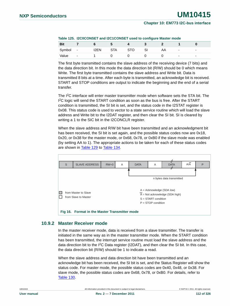
NXP Semiconductors UM10415Chapter 10: EM773 I2C-bus interface
The first byte transmitted contains the slave address of the receiving device (7 bits) and the data direction bit. In this mode the data direction bit (R/W) should be 0 which means Write. The first byte transmitted contains the slave address and Write bit. Data is transmitted 8 bits at a time. After each byte is transmitted, an acknowledge bit is received. START and STOP conditions are output to indicate the beginning and the end of a serial transfer.
The I2C interface will enter master transmitter mode when software sets the STA bit. The I2C logic will send the START condition as soon as the bus is free. After the START condition is transmitted, the SI bit is set, and the status code in the I2STAT register is 0x08. This status code is used to vector to a state service routine which will load the slave address and Write bit to the I2DAT register, and then clear the SI bit. SI is cleared by writing a 1 to the SIC bit in the I2CONCLR register.
When the slave address and R/W bit have been transmitted and an acknowledgment bit has been received, the SI bit is set again, and the possible status codes now are 0x18, 0x20, or 0x38 for the master mode, or 0x68, 0x78, or 0xB0 if the slave mode was enabled (by setting AA to 1). The appropriate actions to be taken for each of these status codes are shown in Table 129 to Table 134.
10.9.2 Master Receiver mode
In the master receiver mode, data is received from a slave transmitter. The transfer is initiated in the same way as in the master transmitter mode. When the START condition has been transmitted, the interrupt service routine must load the slave address and the data direction bit to the I2C Data register (I2DAT), and then clear the SI bit. In this case, the data direction bit (R/W) should be 1 to indicate a read.
When the slave address and data direction bit have been transmitted and an acknowledge bit has been received, the SI bit is set, and the Status Register will show the status code. For master mode, the possible status codes are 0x40, 0x48, or 0x38. For slave mode, the possible status codes are 0x68, 0x78, or 0xB0. For details, refer to Table 130.
Table 125. I2C0CONSET and I2C1CONSET used to configure Master mode
Bit 7 6 5 4 3 2 1 0
Symbol - I2EN STA STO SI AA - -
Value - 1 0 0 0 0 - -
Fig 16. Format in the Master Transmitter mode
A = Acknowledge (SDA low)
A = Not acknowledge (SDA high)
S = START condition
P = STOP condition
S SLAVE ADDRESS RW=0 A DATA A A/A P
from Master to Slave
from Slave to Master
DATA
n bytes data transmitted
UM10415 All information provided in this document is subject to legal disclaimers. © NXP B.V. 2011. All rights reserved.
User manual Rev. 2 — 7 December 2011 112 of 326
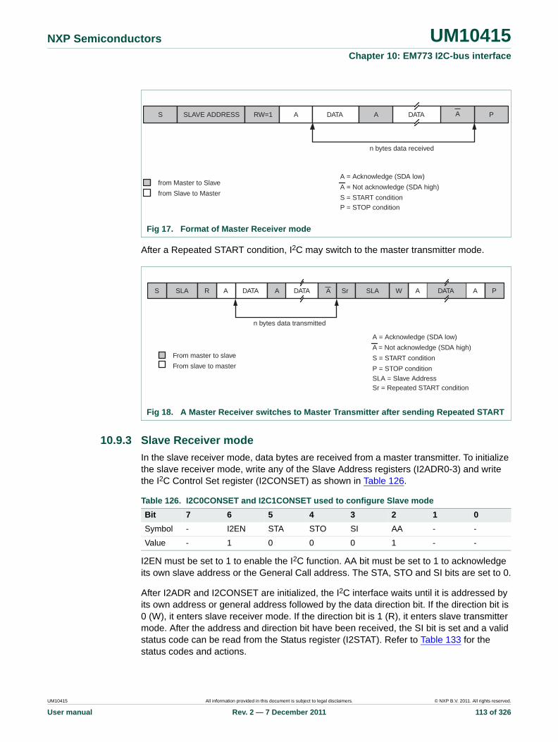
NXP Semiconductors UM10415Chapter 10: EM773 I2C-bus interface
After a Repeated START condition, I2C may switch to the master transmitter mode.
10.9.3 Slave Receiver mode
In the slave receiver mode, data bytes are received from a master transmitter. To initialize the slave receiver mode, write any of the Slave Address registers (I2ADR0-3) and write the I2C Control Set register (I2CONSET) as shown in Table 126.
I2EN must be set to 1 to enable the I2C function. AA bit must be set to 1 to acknowledge its own slave address or the General Call address. The STA, STO and SI bits are set to 0.
After I2ADR and I2CONSET are initialized, the I2C interface waits until it is addressed by its own address or general address followed by the data direction bit. If the direction bit is 0 (W), it enters slave receiver mode. If the direction bit is 1 (R), it enters slave transmitter mode. After the address and direction bit have been received, the SI bit is set and a valid status code can be read from the Status register (I2STAT). Refer to Table 133 for the status codes and actions.
Fig 17. Format of Master Receiver mode
Fig 18. A Master Receiver switches to Master Transmitter after sending Repeated START
DATA
A = Acknowledge (SDA low)
A = Not acknowledge (SDA high)
S = START condition
P = STOP condition
S SLAVE ADDRESS RW=1 A DATA P
n bytes data received
from Master to Slave
from Slave to Master
A A
A = Acknowledge (SDA low)
A = Not acknowledge (SDA high)
S = START condition
P = STOP condition
SLA = Slave AddressSr = Repeated START condition
DATA
n bytes data transmitted
From master to slave
From slave to master
A DATA A ASLA R Sr W PS SLA DATAAA
Table 126. I2C0CONSET and I2C1CONSET used to configure Slave mode
Bit 7 6 5 4 3 2 1 0
Symbol - I2EN STA STO SI AA - -
Value - 1 0 0 0 1 - -
UM10415 All information provided in this document is subject to legal disclaimers. © NXP B.V. 2011. All rights reserved.
User manual Rev. 2 — 7 December 2011 113 of 326
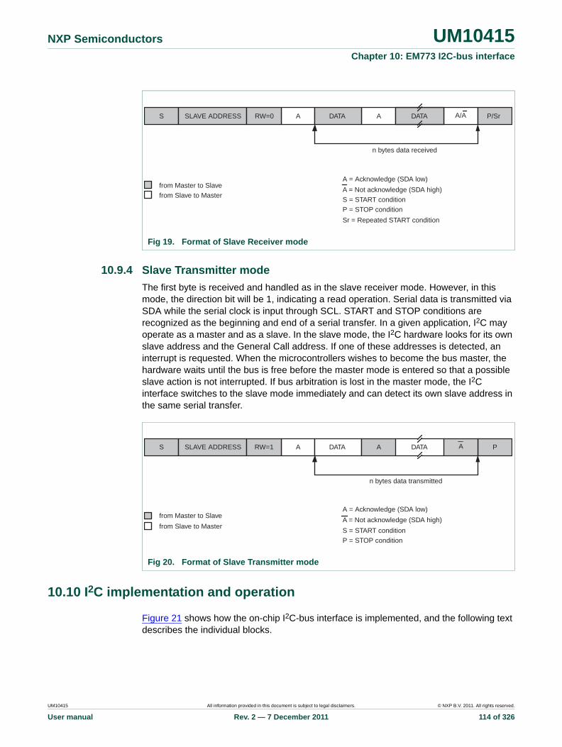
NXP Semiconductors UM10415Chapter 10: EM773 I2C-bus interface
10.9.4 Slave Transmitter mode
The first byte is received and handled as in the slave receiver mode. However, in this mode, the direction bit will be 1, indicating a read operation. Serial data is transmitted via SDA while the serial clock is input through SCL. START and STOP conditions are recognized as the beginning and end of a serial transfer. In a given application, I2C may operate as a master and as a slave. In the slave mode, the I2C hardware looks for its own slave address and the General Call address. If one of these addresses is detected, an interrupt is requested. When the microcontrollers wishes to become the bus master, the hardware waits until the bus is free before the master mode is entered so that a possible slave action is not interrupted. If bus arbitration is lost in the master mode, the I2C interface switches to the slave mode immediately and can detect its own slave address in the same serial transfer.
10.10 I2C implementation and operation
Figure 21 shows how the on-chip I2C-bus interface is implemented, and the following text describes the individual blocks.
Fig 19. Format of Slave Receiver mode
A
A = Acknowledge (SDA low)
A = Not acknowledge (SDA high)
S = START condition
P = STOP condition
Sr = Repeated START condition
A A/A
n bytes data received
from Master to Slave
from Slave to Master
S SLAVE ADDRESS RW=0 DATA P/SrDATA
Fig 20. Format of Slave Transmitter mode
DATA
A = Acknowledge (SDA low)
A = Not acknowledge (SDA high)
S = START condition
P = STOP condition
A DATA
n bytes data transmitted
from Master to Slave
from Slave to Master
S SLAVE ADDRESS RW=1 A PA
UM10415 All information provided in this document is subject to legal disclaimers. © NXP B.V. 2011. All rights reserved.
User manual Rev. 2 — 7 December 2011 114 of 326

NXP Semiconductors UM10415Chapter 10: EM773 I2C-bus interface
10.10.1 Input filters and output stages
Input signals are synchronized with the internal clock, and spikes shorter than three clocks are filtered out.
The output for I2C is a special pad designed to conform to the I2C specification.
Fig 21. I2C serial interface block diagram
AP
B B
US
STATUS REGISTERI2CnSTAT
CONTROL REGISTER and SCL DUTY CYLE REGISTERS
I2CnCONSET, I2CnCONCLR, I2CnSCLH, I2CnSCLL
ADDRESS REGISTERS
MASK and COMPARE
SHIFT REGISTERI2CnDAT
ACK
BIT COUNTER/ARBITRATION and
MONITOR MODEREGISTER
I2CnMMCTRL
SYNC LOGIC
SERIAL CLOCKGENERATOR
TIMING andCONTROL
LOGIC
STATUSDECODER
statusbus
interrupt
PCLKINPUTFILTER
OUTPUTSTAGE
SCL
INPUTFILTER
OUTPUTSTAGE
SDA
I2CnADDR0 to I2CnADDR3
MASK REGISTERSI2CnMASK0 to I2CnMASK3
I2CnDATABUFFER
MATCHALLI2CnMMCTRL[3]
8
8
8
16
UM10415 All information provided in this document is subject to legal disclaimers. © NXP B.V. 2011. All rights reserved.
User manual Rev. 2 — 7 December 2011 115 of 326
NXP Semiconductors UM10415Chapter 10: EM773 I2C-bus interface
10.10.2 Address Registers, I2ADDR0 to I2ADDR3
These registers may be loaded with the 7-bit slave address (7 most significant bits) to which the I2C block will respond when programmed as a slave transmitter or receiver. The LSB (GC) is used to enable General Call address (0x00) recognition. When multiple slave addresses are enabled, the actual address received may be read from the I2DAT register at the state where the own slave address has been received.
10.10.3 Address mask registers, I2MASK0 to I2MASK3
The four mask registers each contain seven active bits (7:1). Any bit in these registers which is set to ‘1’ will cause an automatic compare on the corresponding bit of the received address when it is compared to the I2ADDRn register associated with that mask register. In other words, bits in an I2ADDRn register which are masked are not taken into account in determining an address match.
If the I2ADDRn bit 0 (GC enable bit) is as set and bits(7:1) are all zeroes, then the part will respond to a received address = “0000000” regardless of the state of the associated mask register.
When an address-match interrupt occurs, the processor will have to read the data register (I2DAT) to determine what the received address was that actually caused the match.
10.10.4 Comparator
The comparator compares the received 7-bit slave address with its own slave address (7 most significant bits in I2ADR). It also compares the first received 8-bit byte with the General Call address (0x00). If an equality is found, the appropriate status bits are set and an interrupt is requested.
10.10.5 Shift register, I2DAT
This 8-bit register contains a byte of serial data to be transmitted or a byte which has just been received. Data in I2DAT is always shifted from right to left; the first bit to be transmitted is the MSB (bit 7) and, after a byte has been received, the first bit of received data is located at the MSB of I2DAT. While data is being shifted out, data on the bus is simultaneously being shifted in; I2DAT always contains the last byte present on the bus. Thus, in the event of lost arbitration, the transition from master transmitter to slave receiver is made with the correct data in I2DAT.
10.10.6 Arbitration and synchronization logic
In the master transmitter mode, the arbitration logic checks that every transmitted logic 1 actually appears as a logic 1 on the I2C-bus. If another device on the bus overrules a logic 1 and pulls the SDA line low, arbitration is lost, and the I2C block immediately changes from master transmitter to slave receiver. The I2C block will continue to output clock pulses (on SCL) until transmission of the current serial byte is complete.
Arbitration may also be lost in the master receiver mode. Loss of arbitration in this mode can only occur while the I2C block is returning a “not acknowledge: (logic 1) to the bus. Arbitration is lost when another device on the bus pulls this signal low. Since this can occur only at the end of a serial byte, the I2C block generates no further clock pulses. Figure 22 shows the arbitration procedure.
UM10415 All information provided in this document is subject to legal disclaimers. © NXP B.V. 2011. All rights reserved.
User manual Rev. 2 — 7 December 2011 116 of 326

NXP Semiconductors UM10415Chapter 10: EM773 I2C-bus interface
The synchronization logic will synchronize the serial clock generator with the clock pulses on the SCL line from another device. If two or more master devices generate clock pulses, the “mark” duration is determined by the device that generates the shortest “marks,” and the “space” duration is determined by the device that generates the longest “spaces”. Figure 23 shows the synchronization procedure.
A slave may stretch the space duration to slow down the bus master. The space duration may also be stretched for handshaking purposes. This can be done after each bit or after a complete byte transfer. the I2C block will stretch the SCL space duration after a byte has been transmitted or received and the acknowledge bit has been transferred. The serial interrupt flag (SI) is set, and the stretching continues until the serial interrupt flag is cleared.
10.10.7 Serial clock generator
This programmable clock pulse generator provides the SCL clock pulses when the I2C block is in the master transmitter or master receiver mode. It is switched off when the I2C block is in a slave mode. The I2C output clock frequency and duty cycle is programmable
(1) Another device transmits serial data.
(2) Another device overrules a logic (dotted line) transmitted this I2C master by pulling the SDA line low. Arbitration is lost, and this I2C enters Slave Receiver mode.
(3) This I2C is in Slave Receiver mode but still generates clock pulses until the current byte has been transmitted. This I2C will not generate clock pulses for the next byte. Data on SDA originates from the new master once it has won arbitration.
Fig 22. Arbitration procedure
(1) Another device pulls the SCL line low before this I2C has timed a complete high time. The other device effectively determines the (shorter) HIGH period.
(2) Another device continues to pull the SCL line low after this I2C has timed a complete low time and released SCL. The I2C clock generator is forced to wait until SCL goes HIGH. The other device effectively determines the (longer) LOW period.
(3) The SCL line is released , and the clock generator begins timing the HIGH time.
Fig 23. Serial clock synchronization
SDA line
SCL line1 2 3 4 8 9
ACK
(1) (2)(1) (3)
SDA line
SCL line
(2)
(1)(3)
highperiod
lowperiod
(1)
UM10415 All information provided in this document is subject to legal disclaimers. © NXP B.V. 2011. All rights reserved.
User manual Rev. 2 — 7 December 2011 117 of 326
NXP Semiconductors UM10415Chapter 10: EM773 I2C-bus interface
via the I2C Clock Control Registers. See the description of the I2CSCLL and I2CSCLH registers for details. The output clock pulses have a duty cycle as programmed unless the bus is synchronizing with other SCL clock sources as described above.
10.10.8 Timing and control
The timing and control logic generates the timing and control signals for serial byte handling. This logic block provides the shift pulses for I2DAT, enables the comparator, generates and detects START and STOP conditions, receives and transmits acknowledge bits, controls the master and slave modes, contains interrupt request logic, and monitors the I2C-bus status.
10.10.9 Control register, I2CONSET and I2CONCLR
The I2C control register contains bits used to control the following I2C block functions: start and restart of a serial transfer, termination of a serial transfer, bit rate, address recognition, and acknowledgment.
The contents of the I2C control register may be read as I2CONSET. Writing to I2CONSET will set bits in the I2C control register that correspond to ones in the value written. Conversely, writing to I2CONCLR will clear bits in the I2C control register that correspond to ones in the value written.
10.10.10 Status decoder and status register
The status decoder takes all of the internal status bits and compresses them into a 5-bit code. This code is unique for each I2C-bus status. The 5-bit code may be used to generate vector addresses for fast processing of the various service routines. Each service routine processes a particular bus status. There are 26 possible bus states if all four modes of the I2C block are used. The 5-bit status code is latched into the five most significant bits of the status register when the serial interrupt flag is set (by hardware) and remains stable until the interrupt flag is cleared by software. The three least significant bits of the status register are always zero. If the status code is used as a vector to service routines, then the routines are displaced by eight address locations. Eight bytes of code is sufficient for most of the service routines (see the software example in this section).
10.11 Details of I2C operating modes
The four operating modes are:
• Master Transmitter
• Master Receiver
• Slave Receiver
• Slave Transmitter
Data transfers in each mode of operation are shown in Figure 24, Figure 25, Figure 26, Figure 27, and Figure 28. Table 127 lists abbreviations used in these figures when describing the I2C operating modes.
UM10415 All information provided in this document is subject to legal disclaimers. © NXP B.V. 2011. All rights reserved.
User manual Rev. 2 — 7 December 2011 118 of 326

NXP Semiconductors UM10415Chapter 10: EM773 I2C-bus interface
In Figure 24 to Figure 28, circles are used to indicate when the serial interrupt flag is set. The numbers in the circles show the status code held in the I2STAT register. At these points, a service routine must be executed to continue or complete the serial transfer. These service routines are not critical since the serial transfer is suspended until the serial interrupt flag is cleared by software.
When a serial interrupt routine is entered, the status code in I2STAT is used to branch to the appropriate service routine. For each status code, the required software action and details of the following serial transfer are given in tables from Table 129 to Table 135.
10.11.1 Master Transmitter mode
In the master transmitter mode, a number of data bytes are transmitted to a slave receiver (see Figure 24). Before the master transmitter mode can be entered, I2CON must be initialized as follows:
The I2C rate must also be configured in the I2SCLL and I2SCLH registers. I2EN must be set to logic 1 to enable the I2C block. If the AA bit is reset, the I2C block will not acknowledge its own slave address or the General Call address in the event of another device becoming master of the bus. In other words, if AA is reset, the I2C interface cannot enter a slave mode. STA, STO, and SI must be reset.
Table 127. Abbreviations used to describe an I2C operation
Abbreviation Explanation
S START Condition
SLA 7-bit slave address
R Read bit (HIGH level at SDA)
W Write bit (LOW level at SDA)
A Acknowledge bit (LOW level at SDA)
A Not acknowledge bit (HIGH level at SDA)
Data 8-bit data byte
P STOP condition
Table 128. I2CONSET used to initialize Master Transmitter mode
Bit 7 6 5 4 3 2 1 0
Symbol - I2EN STA STO SI AA - -
Value - 1 0 0 0 x - -
UM10415 All information provided in this document is subject to legal disclaimers. © NXP B.V. 2011. All rights reserved.
User manual Rev. 2 — 7 December 2011 119 of 326

NXP Semiconductors UM10415Chapter 10: EM773 I2C-bus interface
The master transmitter mode may now be entered by setting the STA bit. The I2C logic will now test the I2C-bus and generate a START condition as soon as the bus becomes free. When a START condition is transmitted, the serial interrupt flag (SI) is set, and the status code in the status register (I2STAT) will be 0x08. This status code is used by the interrupt service routine to enter the appropriate state service routine that loads I2DAT with the slave address and the data direction bit (SLA+W). The SI bit in I2CON must then be reset before the serial transfer can continue.
When the slave address and the direction bit have been transmitted and an acknowledgment bit has been received, the serial interrupt flag (SI) is set again, and a number of status codes in I2STAT are possible. There are 0x18, 0x20, or 0x38 for the master mode and also 0x68, 0x78, or 0xB0 if the slave mode was enabled (AA = logic 1). The appropriate action to be taken for each of these status codes is detailed in Table 129. After a Repeated START condition (state 0x10). The I2C block may switch to the master receiver mode by loading I2DAT with SLA+R).
UM10415 All information provided in this document is subject to legal disclaimers. © NXP B.V. 2011. All rights reserved.
User manual Rev. 2 — 7 December 2011 120 of 326

NXP Semiconductors UM10415Chapter 10: EM773 I2C-bus interface
Table 129. Master Transmitter mode
Status Code (I2CSTAT)
Status of the I2C-bus and hardware
Application software response Next action taken by I2C hardware
To/From I2DAT To I2CON
STA STO SI AA
0x08 A START condition has been transmitted.
Load SLA+W; clear STA
X 0 0 X SLA+W will be transmitted; ACK bit will be received.
0x10 A Repeated START condition has been transmitted.
Load SLA+W or X 0 0 X As above.
Load SLA+R; Clear STA
X 0 0 X SLA+R will be transmitted; the I2C block will be switched to MST/REC mode.
0x18 SLA+W has been transmitted; ACK has been received.
Load data byte or 0 0 0 X Data byte will be transmitted; ACK bit will be received.
No I2DAT action or
1 0 0 X Repeated START will be transmitted.
No I2DAT action or
0 1 0 X STOP condition will be transmitted; STO flag will be reset.
No I2DAT action 1 1 0 X STOP condition followed by a START condition will be transmitted; STO flag will be reset.
0x20 SLA+W has been transmitted; NOT ACK has been received.
Load data byte or 0 0 0 X Data byte will be transmitted; ACK bit will be received.
No I2DAT action or
1 0 0 X Repeated START will be transmitted.
No I2DAT action or
0 1 0 X STOP condition will be transmitted; STO flag will be reset.
No I2DAT action 1 1 0 X STOP condition followed by a START condition will be transmitted; STO flag will be reset.
0x28 Data byte in I2DAT has been transmitted; ACK has been received.
Load data byte or 0 0 0 X Data byte will be transmitted; ACK bit will be received.
No I2DAT action or
1 0 0 X Repeated START will be transmitted.
No I2DAT action or
0 1 0 X STOP condition will be transmitted; STO flag will be reset.
No I2DAT action 1 1 0 X STOP condition followed by a START condition will be transmitted; STO flag will be reset.
0x30 Data byte in I2DAT has been transmitted; NOT ACK has been received.
Load data byte or 0 0 0 X Data byte will be transmitted; ACK bit will be received.
No I2DAT action or
1 0 0 X Repeated START will be transmitted.
No I2DAT action or
0 1 0 X STOP condition will be transmitted; STO flag will be reset.
No I2DAT action 1 1 0 X STOP condition followed by a START condition will be transmitted; STO flag will be reset.
0x38 Arbitration lost in SLA+R/W or Data bytes.
No I2DAT action or
0 0 0 X I2C-bus will be released; not addressed slave will be entered.
No I2DAT action 1 0 0 X A START condition will be transmitted when the bus becomes free.
UM10415 All information provided in this document is subject to legal disclaimers. © NXP B.V. 2011. All rights reserved.
User manual Rev. 2 — 7 December 2011 121 of 326

NXP Semiconductors UM10415Chapter 10: EM773 I2C-bus interface
Fig 24. Format and states in the Master Transmitter mode
DATA
A
R
WSLAS
DATAAWSLA
to Masterreceivemode,entry= MR
MT
to correspondingstates in Slave mode
A OR AA OR A
A
other Mastercontinues
other Mastercontinues
A other Mastercontinues
20H
08H 18H 28H
30H
10H
68H 78H B0H
38H 38H
arbitration lostin Slaveaddress orData byte
NotAcknowledgereceived after aData byte
NotAcknowledgereceived afterthe Slaveaddress
next transferstarted with aRepeated Startcondition
arbitration lostandaddressed asSlave
successfultransmissionto a SlaveReceiver
from Master to Slave
from Slave to Master
any number of data bytes and their associated Acknowledge bits
nthis number (contained in I2STA) corresponds to a defined state of theI2C bus
A P
P
S P
UM10415 All information provided in this document is subject to legal disclaimers. © NXP B.V. 2011. All rights reserved.
User manual Rev. 2 — 7 December 2011 122 of 326

NXP Semiconductors UM10415Chapter 10: EM773 I2C-bus interface
10.11.2 Master Receiver mode
In the master receiver mode, a number of data bytes are received from a slave transmitter (see Figure 25). The transfer is initialized as in the master transmitter mode. When the START condition has been transmitted, the interrupt service routine must load I2DAT with the 7-bit slave address and the data direction bit (SLA+R). The SI bit in I2CON must then be cleared before the serial transfer can continue.
When the slave address and the data direction bit have been transmitted and an acknowledgment bit has been received, the serial interrupt flag (SI) is set again, and a number of status codes in I2STAT are possible. These are 0x40, 0x48, or 0x38 for the master mode and also 0x68, 0x78, or 0xB0 if the slave mode was enabled (AA = 1). The appropriate action to be taken for each of these status codes is detailed in Table 130. After a Repeated START condition (state 0x10), the I2C block may switch to the master transmitter mode by loading I2DAT with SLA+W.
UM10415 All information provided in this document is subject to legal disclaimers. © NXP B.V. 2011. All rights reserved.
User manual Rev. 2 — 7 December 2011 123 of 326
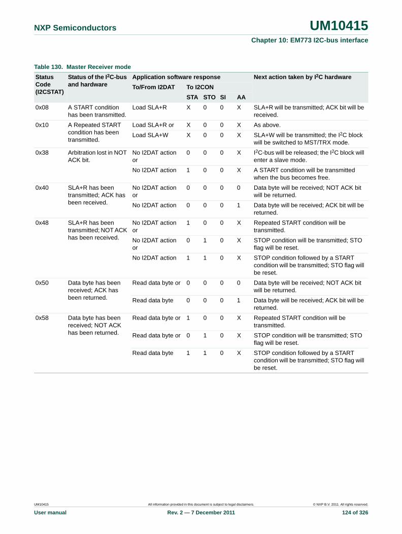
NXP Semiconductors UM10415Chapter 10: EM773 I2C-bus interface
Table 130. Master Receiver mode
Status Code (I2CSTAT)
Status of the I2C-bus and hardware
Application software response Next action taken by I2C hardware
To/From I2DAT To I2CON
STA STO SI AA
0x08 A START condition has been transmitted.
Load SLA+R X 0 0 X SLA+R will be transmitted; ACK bit will be received.
0x10 A Repeated START condition has been transmitted.
Load SLA+R or X 0 0 X As above.
Load SLA+W X 0 0 X SLA+W will be transmitted; the I2C block will be switched to MST/TRX mode.
0x38 Arbitration lost in NOT ACK bit.
No I2DAT action or
0 0 0 X I2C-bus will be released; the I2C block will enter a slave mode.
No I2DAT action 1 0 0 X A START condition will be transmitted when the bus becomes free.
0x40 SLA+R has been transmitted; ACK has been received.
No I2DAT action or
0 0 0 0 Data byte will be received; NOT ACK bit will be returned.
No I2DAT action 0 0 0 1 Data byte will be received; ACK bit will be returned.
0x48 SLA+R has been transmitted; NOT ACK has been received.
No I2DAT action or
1 0 0 X Repeated START condition will be transmitted.
No I2DAT action or
0 1 0 X STOP condition will be transmitted; STO flag will be reset.
No I2DAT action 1 1 0 X STOP condition followed by a START condition will be transmitted; STO flag will be reset.
0x50 Data byte has been received; ACK has been returned.
Read data byte or 0 0 0 0 Data byte will be received; NOT ACK bit will be returned.
Read data byte 0 0 0 1 Data byte will be received; ACK bit will be returned.
0x58 Data byte has been received; NOT ACK has been returned.
Read data byte or 1 0 0 X Repeated START condition will be transmitted.
Read data byte or 0 1 0 X STOP condition will be transmitted; STO flag will be reset.
Read data byte 1 1 0 X STOP condition followed by a START condition will be transmitted; STO flag will be reset.
UM10415 All information provided in this document is subject to legal disclaimers. © NXP B.V. 2011. All rights reserved.
User manual Rev. 2 — 7 December 2011 124 of 326

NXP Semiconductors UM10415Chapter 10: EM773 I2C-bus interface
Fig 25. Format and states in the Master Receiver mode
A
to Mastertransmit
mode, entry= MT
MR
to correspondingstates in Slave
mode
ARSLAS
RSLAS
W
AA OR A
A P
other Mastercontinues
other Mastercontinues
A other Mastercontinues
48H
40H 58H
10H
68H 78H B0H
38H 38H
arbitration lost inSlave address orAcknowledge bit
Not Acknowledgereceived after theSlave address
next transferstarted with aRepeated Startcondition
arbitration lostand addressedas Slave
successfultransmission toa Slavetransmitter
from Master to Slave
from Slave to Master
any number of data bytes and their associatedAcknowledge bits
nthis number (contained in I2STA) corresponds to a defined state ofthe I2C bus
DATAADATA
50H
ADATA
P
08H
UM10415 All information provided in this document is subject to legal disclaimers. © NXP B.V. 2011. All rights reserved.
User manual Rev. 2 — 7 December 2011 125 of 326

NXP Semiconductors UM10415Chapter 10: EM773 I2C-bus interface
10.11.3 Slave Receiver mode
In the slave receiver mode, a number of data bytes are received from a master transmitter (see Figure 26). To initiate the slave receiver mode, I2ADR and I2CON must be loaded as follows:
The upper 7 bits are the address to which the I2C block will respond when addressed by a master. If the LSB (GC) is set, the I2C block will respond to the General Call address (0x00); otherwise it ignores the General Call address.
The I2C-bus rate settings do not affect the I2C block in the slave mode. I2EN must be set to logic 1 to enable the I2C block. The AA bit must be set to enable the I2C block to acknowledge its own slave address or the General Call address. STA, STO, and SI must be reset.
When I2ADR and I2CON have been initialized, the I2C block waits until it is addressed by its own slave address followed by the data direction bit which must be “0” (W) for the I2C block to operate in the slave receiver mode. After its own slave address and the W bit have been received, the serial interrupt flag (SI) is set and a valid status code can be read from I2STAT. This status code is used to vector to a state service routine. The appropriate action to be taken for each of these status codes is detailed in Table 133. The slave receiver mode may also be entered if arbitration is lost while the I2C block is in the master mode (see status 0x68 and 0x78).
If the AA bit is reset during a transfer, the I2C block will return a not acknowledge (logic 1) to SDA after the next received data byte. While AA is reset, the I2C block does not respond to its own slave address or a General Call address. However, the I2C-bus is still monitored and address recognition may be resumed at any time by setting AA. This means that the AA bit may be used to temporarily isolate the I2C block from the I2C-bus.
Table 131. I2C0ADR and I2C1ADR usage in Slave Receiver mode
Bit 7 6 5 4 3 2 1 0
Symbol own slave 7-bit address GC
Table 132. I2C0CONSET and I2C1CONSET used to initialize Slave Receiver mode
Bit 7 6 5 4 3 2 1 0
Symbol - I2EN STA STO SI AA - -
Value - 1 0 0 0 1 - -
UM10415 All information provided in this document is subject to legal disclaimers. © NXP B.V. 2011. All rights reserved.
User manual Rev. 2 — 7 December 2011 126 of 326
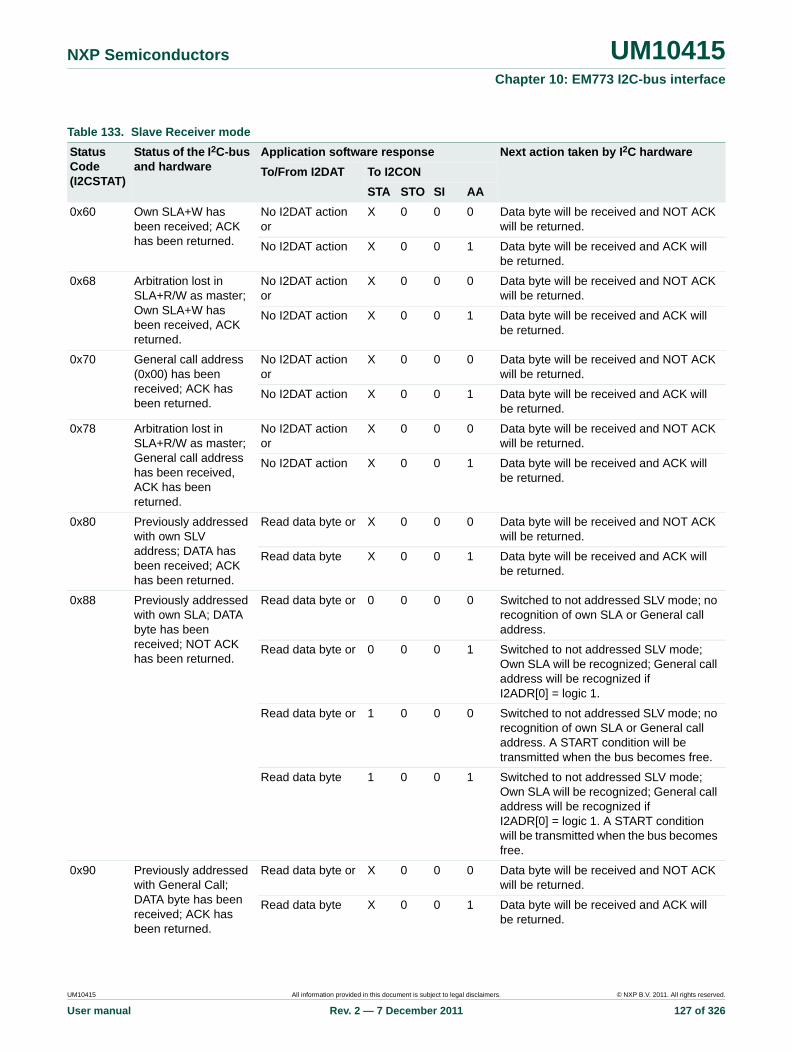
NXP Semiconductors UM10415Chapter 10: EM773 I2C-bus interface
Table 133. Slave Receiver mode
Status Code (I2CSTAT)
Status of the I2C-bus and hardware
Application software response Next action taken by I2C hardware
To/From I2DAT To I2CON
STA STO SI AA
0x60 Own SLA+W has been received; ACK has been returned.
No I2DAT action or
X 0 0 0 Data byte will be received and NOT ACK will be returned.
No I2DAT action X 0 0 1 Data byte will be received and ACK will be returned.
0x68 Arbitration lost in SLA+R/W as master; Own SLA+W has been received, ACK returned.
No I2DAT action or
X 0 0 0 Data byte will be received and NOT ACK will be returned.
No I2DAT action X 0 0 1 Data byte will be received and ACK will be returned.
0x70 General call address (0x00) has been received; ACK has been returned.
No I2DAT action or
X 0 0 0 Data byte will be received and NOT ACK will be returned.
No I2DAT action X 0 0 1 Data byte will be received and ACK will be returned.
0x78 Arbitration lost in SLA+R/W as master; General call address has been received, ACK has been returned.
No I2DAT action or
X 0 0 0 Data byte will be received and NOT ACK will be returned.
No I2DAT action X 0 0 1 Data byte will be received and ACK will be returned.
0x80 Previously addressed with own SLV address; DATA has been received; ACK has been returned.
Read data byte or X 0 0 0 Data byte will be received and NOT ACK will be returned.
Read data byte X 0 0 1 Data byte will be received and ACK will be returned.
0x88 Previously addressed with own SLA; DATA byte has been received; NOT ACK has been returned.
Read data byte or 0 0 0 0 Switched to not addressed SLV mode; no recognition of own SLA or General call address.
Read data byte or 0 0 0 1 Switched to not addressed SLV mode; Own SLA will be recognized; General call address will be recognized if I2ADR[0] = logic 1.
Read data byte or 1 0 0 0 Switched to not addressed SLV mode; no recognition of own SLA or General call address. A START condition will be transmitted when the bus becomes free.
Read data byte 1 0 0 1 Switched to not addressed SLV mode; Own SLA will be recognized; General call address will be recognized if I2ADR[0] = logic 1. A START condition will be transmitted when the bus becomes free.
0x90 Previously addressed with General Call; DATA byte has been received; ACK has been returned.
Read data byte or X 0 0 0 Data byte will be received and NOT ACK will be returned.
Read data byte X 0 0 1 Data byte will be received and ACK will be returned.
UM10415 All information provided in this document is subject to legal disclaimers. © NXP B.V. 2011. All rights reserved.
User manual Rev. 2 — 7 December 2011 127 of 326
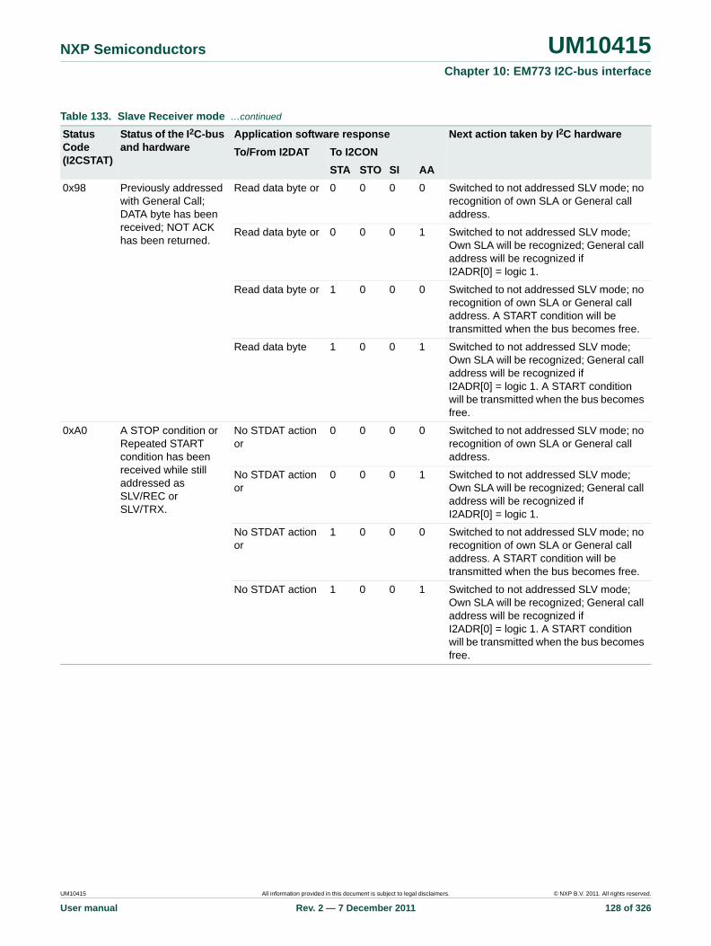
NXP Semiconductors UM10415Chapter 10: EM773 I2C-bus interface
0x98 Previously addressed with General Call; DATA byte has been received; NOT ACK has been returned.
Read data byte or 0 0 0 0 Switched to not addressed SLV mode; no recognition of own SLA or General call address.
Read data byte or 0 0 0 1 Switched to not addressed SLV mode; Own SLA will be recognized; General call address will be recognized if I2ADR[0] = logic 1.
Read data byte or 1 0 0 0 Switched to not addressed SLV mode; no recognition of own SLA or General call address. A START condition will be transmitted when the bus becomes free.
Read data byte 1 0 0 1 Switched to not addressed SLV mode; Own SLA will be recognized; General call address will be recognized if I2ADR[0] = logic 1. A START condition will be transmitted when the bus becomes free.
0xA0 A STOP condition or Repeated START condition has been received while still addressed as SLV/REC or SLV/TRX.
No STDAT action or
0 0 0 0 Switched to not addressed SLV mode; no recognition of own SLA or General call address.
No STDAT action or
0 0 0 1 Switched to not addressed SLV mode; Own SLA will be recognized; General call address will be recognized if I2ADR[0] = logic 1.
No STDAT action or
1 0 0 0 Switched to not addressed SLV mode; no recognition of own SLA or General call address. A START condition will be transmitted when the bus becomes free.
No STDAT action 1 0 0 1 Switched to not addressed SLV mode; Own SLA will be recognized; General call address will be recognized if I2ADR[0] = logic 1. A START condition will be transmitted when the bus becomes free.
Table 133. Slave Receiver mode …continued
Status Code (I2CSTAT)
Status of the I2C-bus and hardware
Application software response Next action taken by I2C hardware
To/From I2DAT To I2CON
STA STO SI AA
UM10415 All information provided in this document is subject to legal disclaimers. © NXP B.V. 2011. All rights reserved.
User manual Rev. 2 — 7 December 2011 128 of 326

NXP Semiconductors UM10415Chapter 10: EM773 I2C-bus interface
Fig 26. Format and states in the Slave Receiver mode
A
A P OR SAWSLAS
P OR SA
A
68H
60H 80H
88H
reception of theGeneral Call addressand one or more Databytes
arbitration lost asMaster and addressedas Slave
last data bytereceived is Notacknowledged
arbitration lost asMaster and addressedas Slave by GeneralCall
reception of the ownSlave address and oneor more Data bytes allare acknowledged
from Master to Slave
from Slave to Master
any number of data bytes and their associated Acknowledge bits
nthis number (contained in I2STA) corresponds to a defined state of the I2Cbus
DATAADATA
80H A0H
last data byte is Notacknowledged
A P OR SA
70h 90h
DATAADATA
90h A0H
GENERAL CALL
A
98h
P OR S
A
78h
DATA
UM10415 All information provided in this document is subject to legal disclaimers. © NXP B.V. 2011. All rights reserved.
User manual Rev. 2 — 7 December 2011 129 of 326
NXP Semiconductors UM10415Chapter 10: EM773 I2C-bus interface
10.11.4 Slave Transmitter mode
In the slave transmitter mode, a number of data bytes are transmitted to a master receiver (see Figure 27). Data transfer is initialized as in the slave receiver mode. When I2ADR and I2CON have been initialized, the I2C block waits until it is addressed by its own slave address followed by the data direction bit which must be “1” (R) for the I2C block to operate in the slave transmitter mode. After its own slave address and the R bit have been received, the serial interrupt flag (SI) is set and a valid status code can be read from I2STAT. This status code is used to vector to a state service routine, and the appropriate action to be taken for each of these status codes is detailed in Table 134. The slave transmitter mode may also be entered if arbitration is lost while the I2C block is in the master mode (see state 0xB0).
If the AA bit is reset during a transfer, the I2C block will transmit the last byte of the transfer and enter state 0xC0 or 0xC8. The I2C block is switched to the not addressed slave mode and will ignore the master receiver if it continues the transfer. Thus the master receiver receives all 1s as serial data. While AA is reset, the I2C block does not respond to its own slave address or a General Call address. However, the I2C-bus is still monitored, and address recognition may be resumed at any time by setting AA. This means that the AA bit may be used to temporarily isolate the I2C block from the I2C-bus.
UM10415 All information provided in this document is subject to legal disclaimers. © NXP B.V. 2011. All rights reserved.
User manual Rev. 2 — 7 December 2011 130 of 326

NXP Semiconductors UM10415Chapter 10: EM773 I2C-bus interface
Table 134. Slave Transmitter mode
Status Code (I2CSTAT)
Status of the I2C-bus and hardware
Application software response Next action taken by I2C hardware
To/From I2DAT To I2CON
STA STO SI AA
0xA8 Own SLA+R has been received; ACK has been returned.
Load data byte or X 0 0 0 Last data byte will be transmitted and ACK bit will be received.
Load data byte X 0 0 1 Data byte will be transmitted; ACK will be received.
0xB0 Arbitration lost in SLA+R/W as master; Own SLA+R has been received, ACK has been returned.
Load data byte or X 0 0 0 Last data byte will be transmitted and ACK bit will be received.
Load data byte X 0 0 1 Data byte will be transmitted; ACK bit will be received.
0xB8 Data byte in I2DAT has been transmitted; ACK has been received.
Load data byte or X 0 0 0 Last data byte will be transmitted and ACK bit will be received.
Load data byte X 0 0 1 Data byte will be transmitted; ACK bit will be received.
0xC0 Data byte in I2DAT has been transmitted; NOT ACK has been received.
No I2DAT action or
0 0 0 0 Switched to not addressed SLV mode; no recognition of own SLA or General call address.
No I2DAT action or
0 0 0 1 Switched to not addressed SLV mode; Own SLA will be recognized; General call address will be recognized if I2ADR[0] = logic 1.
No I2DAT action or
1 0 0 0 Switched to not addressed SLV mode; no recognition of own SLA or General call address. A START condition will be transmitted when the bus becomes free.
No I2DAT action 1 0 0 1 Switched to not addressed SLV mode; Own SLA will be recognized; General call address will be recognized if I2ADR[0] = logic 1. A START condition will be transmitted when the bus becomes free.
0xC8 Last data byte in I2DAT has been transmitted (AA = 0); ACK has been received.
No I2DAT action or
0 0 0 0 Switched to not addressed SLV mode; no recognition of own SLA or General call address.
No I2DAT action or
0 0 0 1 Switched to not addressed SLV mode; Own SLA will be recognized; General call address will be recognized if I2ADR[0] = logic 1.
No I2DAT action or
1 0 0 0 Switched to not addressed SLV mode; no recognition of own SLA or General call address. A START condition will be transmitted when the bus becomes free.
No I2DAT action 1 0 0 01 Switched to not addressed SLV mode; Own SLA will be recognized; General call address will be recognized if I2ADR.0 = logic 1. A START condition will be transmitted when the bus becomes free.
UM10415 All information provided in this document is subject to legal disclaimers. © NXP B.V. 2011. All rights reserved.
User manual Rev. 2 — 7 December 2011 131 of 326
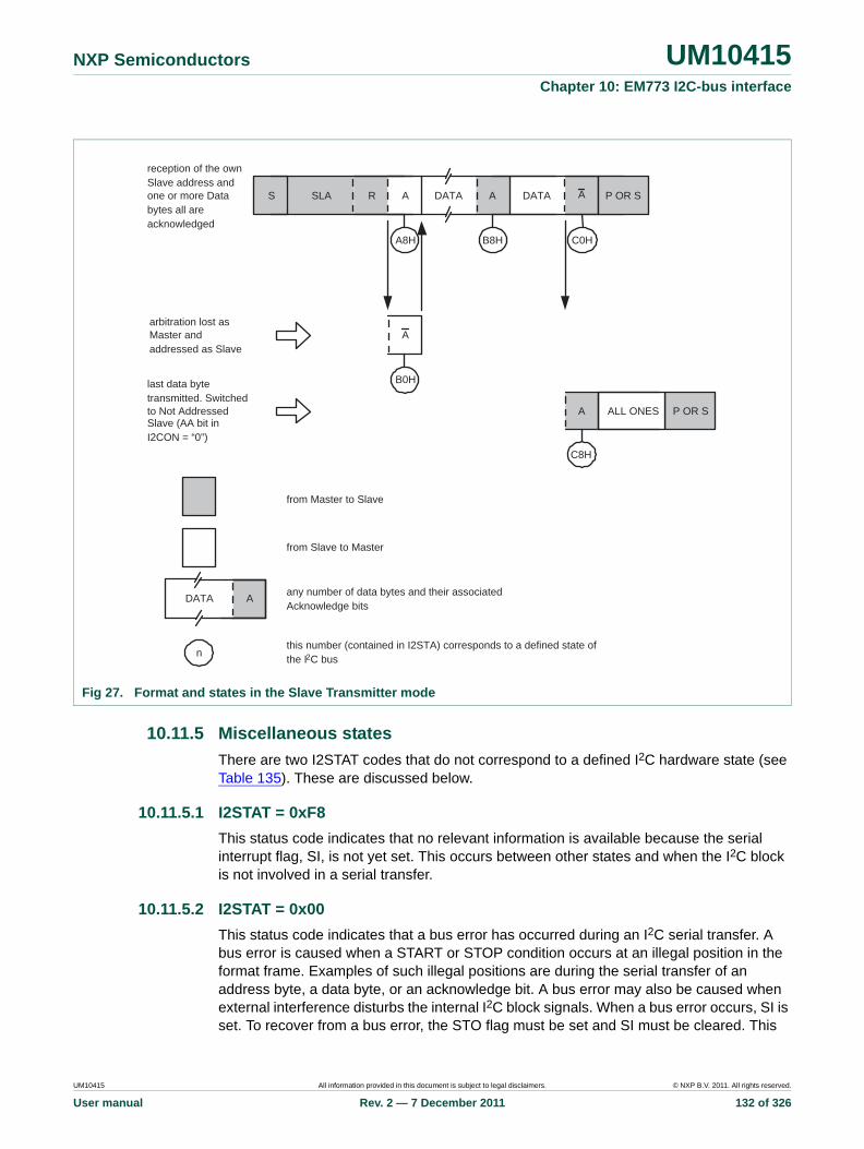
NXP Semiconductors UM10415Chapter 10: EM773 I2C-bus interface
10.11.5 Miscellaneous states
There are two I2STAT codes that do not correspond to a defined I2C hardware state (see Table 135). These are discussed below.
10.11.5.1 I2STAT = 0xF8
This status code indicates that no relevant information is available because the serial interrupt flag, SI, is not yet set. This occurs between other states and when the I2C block is not involved in a serial transfer.
10.11.5.2 I2STAT = 0x00
This status code indicates that a bus error has occurred during an I2C serial transfer. A bus error is caused when a START or STOP condition occurs at an illegal position in the format frame. Examples of such illegal positions are during the serial transfer of an address byte, a data byte, or an acknowledge bit. A bus error may also be caused when external interference disturbs the internal I2C block signals. When a bus error occurs, SI is set. To recover from a bus error, the STO flag must be set and SI must be cleared. This
Fig 27. Format and states in the Slave Transmitter mode
DATA AARSLAS
P OR SA
A
B0H
A8H C0H
C8H
last data bytetransmitted. Switchedto Not AddressedSlave (AA bit inI2CON = “0”)
arbitration lost asMaster andaddressed as Slave
reception of the ownSlave address andone or more Databytes all areacknowledged
from Master to Slave
from Slave to Master
any number of data bytes and their associatedAcknowledge bits
nthis number (contained in I2STA) corresponds to a defined state ofthe I2C bus
ADATA
B8H
ALL ONES
ADATA
P OR S
UM10415 All information provided in this document is subject to legal disclaimers. © NXP B.V. 2011. All rights reserved.
User manual Rev. 2 — 7 December 2011 132 of 326

NXP Semiconductors UM10415Chapter 10: EM773 I2C-bus interface
causes the I2C block to enter the “not addressed” slave mode (a defined state) and to clear the STO flag (no other bits in I2CON are affected). The SDA and SCL lines are released (a STOP condition is not transmitted).
10.11.6 Some special cases
The I2C hardware has facilities to handle the following special cases that may occur during a serial transfer:
• Simultaneous Repeated START conditions from two masters
• Data transfer after loss of arbitration
• Forced access to the I2C-bus
• I2C-bus obstructed by a LOW level on SCL or SDA
• Bus error
10.11.6.1 Simultaneous Repeated START conditions from two masters
A Repeated START condition may be generated in the master transmitter or master receiver modes. A special case occurs if another master simultaneously generates a Repeated START condition (see Figure 28). Until this occurs, arbitration is not lost by either master since they were both transmitting the same data.
If the I2C hardware detects a Repeated START condition on the I2C-bus before generating a Repeated START condition itself, it will release the bus, and no interrupt request is generated. If another master frees the bus by generating a STOP condition, the I2C block will transmit a normal START condition (state 0x08), and a retry of the total serial data transfer can commence.
Table 135. Miscellaneous States
Status Code (I2CSTAT)
Status of the I2C-bus and hardware
Application software response Next action taken by I2C hardware
To/From I2DAT To I2CON
STA STO SI AA
0xF8 No relevant state information available; SI = 0.
No I2DAT action No I2CON action Wait or proceed current transfer.
0x00 Bus error during MST or selected slave modes, due to an illegal START or STOP condition. State 0x00 can also occur when interference causes the I2C block to enter an undefined state.
No I2DAT action 0 1 0 X Only the internal hardware is affected in the MST or addressed SLV modes. In all cases, the bus is released and the I2C block is switched to the not addressed SLV mode. STO is reset.
UM10415 All information provided in this document is subject to legal disclaimers. © NXP B.V. 2011. All rights reserved.
User manual Rev. 2 — 7 December 2011 133 of 326

NXP Semiconductors UM10415Chapter 10: EM773 I2C-bus interface
10.11.6.2 Data transfer after loss of arbitration
Arbitration may be lost in the master transmitter and master receiver modes (see Figure 22). Loss of arbitration is indicated by the following states in I2STAT; 0x38, 0x68, 0x78, and 0xB0 (see Figure 24 and Figure 25).
If the STA flag in I2CON is set by the routines which service these states, then, if the bus is free again, a START condition (state 0x08) is transmitted without intervention by the CPU, and a retry of the total serial transfer can commence.
10.11.6.3 Forced access to the I2C-bus
In some applications, it may be possible for an uncontrolled source to cause a bus hang-up. In such situations, the problem may be caused by interference, temporary interruption of the bus or a temporary short-circuit between SDA and SCL.
If an uncontrolled source generates a superfluous START or masks a STOP condition, then the I2C-bus stays busy indefinitely. If the STA flag is set and bus access is not obtained within a reasonable amount of time, then a forced access to the I2C-bus is possible. This is achieved by setting the STO flag while the STA flag is still set. No STOP condition is transmitted. The I2C hardware behaves as if a STOP condition was received and is able to transmit a START condition. The STO flag is cleared by hardware (see Figure 29).
Fig 28. Simultaneous Repeated START conditions from two masters
SLAAWSLAS
18H 08H
ADATA
28H08H
OTHER MASTERCONTINUES
other Master sendsrepeated START earlier
S
retry
S P
Fig 29. Forced access to a busy I2C-bus
SDA line
SCL line
STA flag
STO flag
time limit
startcondition
UM10415 All information provided in this document is subject to legal disclaimers. © NXP B.V. 2011. All rights reserved.
User manual Rev. 2 — 7 December 2011 134 of 326

NXP Semiconductors UM10415Chapter 10: EM773 I2C-bus interface
10.11.6.4 I2C-bus obstructed by a LOW level on SCL or SDA
An I2C-bus hang-up can occur if either the SDA or SCL line is held LOW by any device on the bus. If the SCL line is obstructed (pulled LOW) by a device on the bus, no further serial transfer is possible, and the problem must be resolved by the device that is pulling the SCL bus line LOW.
Typically, the SDA line may be obstructed by another device on the bus that has become out of synchronization with the current bus master by either missing a clock, or by sensing a noise pulse as a clock. In this case, the problem can be solved by transmitting additional clock pulses on the SCL line (see Figure 30). The I2C interface does not include a dedicated timeout timer to detect an obstructed bus, but this can be implemented using another timer in the system. When detected, software can force clocks (up to 9 may be required) on SCL until SDA is released by the offending device. At that point, the slave may still be out of synchronization, so a START should be generated to insure that all I2C peripherals are synchronized.
10.11.6.5 Bus error
A bus error occurs when a START or STOP condition is detected at an illegal position in the format frame. Examples of illegal positions are during the serial transfer of an address byte, a data bit, or an acknowledge bit.
The I2C hardware only reacts to a bus error when it is involved in a serial transfer either as a master or an addressed slave. When a bus error is detected, the I2C block immediately switches to the not addressed slave mode, releases the SDA and SCL lines, sets the interrupt flag, and loads the status register with 0x00. This status code may be used to vector to a state service routine which either attempts the aborted serial transfer again or simply recovers from the error condition as shown in Table 135.
10.11.7 I2C state service routines
This section provides examples of operations that must be performed by various I2C state service routines. This includes:
• Initialization of the I2C block after a Reset.
• I2C Interrupt Service
• The 26 state service routines providing support for all four I2C operating modes.
(1) Unsuccessful attempt to send a START condition.
(2) SDA line is released.
(3) Successful attempt to send a START condition. State 08H is entered.
Fig 30. Recovering from a bus obstruction caused by a LOW level on SDA
SDA line
SCL line
(1)
(2)
(1)
(3)STA flag
startcondition
UM10415 All information provided in this document is subject to legal disclaimers. © NXP B.V. 2011. All rights reserved.
User manual Rev. 2 — 7 December 2011 135 of 326

NXP Semiconductors UM10415Chapter 10: EM773 I2C-bus interface
10.11.8 Initialization
In the initialization example, the I2C block is enabled for both master and slave modes. For each mode, a buffer is used for transmission and reception. The initialization routine performs the following functions:
• I2ADR is loaded with the part’s own slave address and the General Call bit (GC)
• The I2C interrupt enable and interrupt priority bits are set
• The slave mode is enabled by simultaneously setting the I2EN and AA bits in I2CON and the serial clock frequency (for master modes) is defined by is defined by loading the I2SCLH and I2SCLL registers. The master routines must be started in the main program.
The I2C hardware now begins checking the I2C-bus for its own slave address and General Call. If the General Call or the own slave address is detected, an interrupt is requested and I2STAT is loaded with the appropriate state information.
10.11.9 I2C interrupt service
When the I2C interrupt is entered, I2STAT contains a status code which identifies one of the 26 state services to be executed.
10.11.10 The state service routines
Each state routine is part of the I2C interrupt routine and handles one of the 26 states.
10.11.11 Adapting state services to an application
The state service examples show the typical actions that must be performed in response to the 26 I2C state codes. If one or more of the four I2C operating modes are not used, the associated state services can be omitted, as long as care is taken that the those states can never occur.
In an application, it may be desirable to implement some kind of timeout during I2C operations, in order to trap an inoperative bus or a lost service routine.
10.12 Software example
10.12.1 Initialization routine
Example to initialize I2C Interface as a Slave and/or Master.
1. Load I2ADR with own Slave Address, enable General Call recognition if needed.
2. Enable I2C interrupt.
3. Write 0x44 to I2CONSET to set the I2EN and AA bits, enabling Slave functions. For Master only functions, write 0x40 to I2CONSET.
10.12.2 Start Master Transmit function
Begin a Master Transmit operation by setting up the buffer, pointer, and data count, then initiating a START.
1. Initialize Master data counter.
UM10415 All information provided in this document is subject to legal disclaimers. © NXP B.V. 2011. All rights reserved.User manual Rev. 2 — 7 December 2011 136 of 326
NXP Semiconductors UM10415Chapter 10: EM773 I2C-bus interface
2. Set up the Slave Address to which data will be transmitted, and add the Write bit.
3. Write 0x20 to I2CONSET to set the STA bit.
4. Set up data to be transmitted in Master Transmit buffer.
5. Initialize the Master data counter to match the length of the message being sent.
6. Exit
10.12.3 Start Master Receive function
Begin a Master Receive operation by setting up the buffer, pointer, and data count, then initiating a START.
1. Initialize Master data counter.
2. Set up the Slave Address to which data will be transmitted, and add the Read bit.
3. Write 0x20 to I2CONSET to set the STA bit.
4. Set up the Master Receive buffer.
5. Initialize the Master data counter to match the length of the message to be received.
6. Exit
10.12.4 I2C interrupt routine
Determine the I2C state and which state routine will be used to handle it.
1. Read the I2C status from I2STA.
2. Use the status value to branch to one of 26 possible state routines.
10.12.5 Non mode specific states
10.12.5.1 State: 0x00
Bus Error. Enter not addressed Slave mode and release bus.
1. Write 0x14 to I2CONSET to set the STO and AA bits.
2. Write 0x08 to I2CONCLR to clear the SI flag.
3. Exit
10.12.5.2 Master States
State 08 and State 10 are for both Master Transmit and Master Receive modes. The R/W bit decides whether the next state is within Master Transmit mode or Master Receive mode.
10.12.5.3 State: 0x08
A START condition has been transmitted. The Slave Address + R/W bit will be transmitted, an ACK bit will be received.
1. Write Slave Address with R/W bit to I2DAT.
2. Write 0x04 to I2CONSET to set the AA bit.
3. Write 0x08 to I2CONCLR to clear the SI flag.
4. Set up Master Transmit mode data buffer.
UM10415 All information provided in this document is subject to legal disclaimers. © NXP B.V. 2011. All rights reserved.
User manual Rev. 2 — 7 December 2011 137 of 326

NXP Semiconductors UM10415Chapter 10: EM773 I2C-bus interface
5. Set up Master Receive mode data buffer.
6. Initialize Master data counter.
7. Exit
10.12.5.4 State: 0x10
A Repeated START condition has been transmitted. The Slave Address + R/W bit will be transmitted, an ACK bit will be received.
1. Write Slave Address with R/W bit to I2DAT.
2. Write 0x04 to I2CONSET to set the AA bit.
3. Write 0x08 to I2CONCLR to clear the SI flag.
4. Set up Master Transmit mode data buffer.
5. Set up Master Receive mode data buffer.
6. Initialize Master data counter.
7. Exit
10.12.6 Master Transmitter states
10.12.6.1 State: 0x18
Previous state was State 8 or State 10, Slave Address + Write has been transmitted, ACK has been received. The first data byte will be transmitted, an ACK bit will be received.
1. Load I2DAT with first data byte from Master Transmit buffer.
2. Write 0x04 to I2CONSET to set the AA bit.
3. Write 0x08 to I2CONCLR to clear the SI flag.
4. Increment Master Transmit buffer pointer.
5. Exit
10.12.6.2 State: 0x20
Slave Address + Write has been transmitted, NOT ACK has been received. A STOP condition will be transmitted.
1. Write 0x14 to I2CONSET to set the STO and AA bits.
2. Write 0x08 to I2CONCLR to clear the SI flag.
3. Exit
10.12.6.3 State: 0x28
Data has been transmitted, ACK has been received. If the transmitted data was the last data byte then transmit a STOP condition, otherwise transmit the next data byte.
1. Decrement the Master data counter, skip to step 5 if not the last data byte.
2. Write 0x14 to I2CONSET to set the STO and AA bits.
3. Write 0x08 to I2CONCLR to clear the SI flag.
4. Exit
5. Load I2DAT with next data byte from Master Transmit buffer.
UM10415 All information provided in this document is subject to legal disclaimers. © NXP B.V. 2011. All rights reserved.
User manual Rev. 2 — 7 December 2011 138 of 326

NXP Semiconductors UM10415Chapter 10: EM773 I2C-bus interface
6. Write 0x04 to I2CONSET to set the AA bit.
7. Write 0x08 to I2CONCLR to clear the SI flag.
8. Increment Master Transmit buffer pointer
9. Exit
10.12.6.4 State: 0x30
Data has been transmitted, NOT ACK received. A STOP condition will be transmitted.
1. Write 0x14 to I2CONSET to set the STO and AA bits.
2. Write 0x08 to I2CONCLR to clear the SI flag.
3. Exit
10.12.6.5 State: 0x38
Arbitration has been lost during Slave Address + Write or data. The bus has been released and not addressed Slave mode is entered. A new START condition will be transmitted when the bus is free again.
1. Write 0x24 to I2CONSET to set the STA and AA bits.
2. Write 0x08 to I2CONCLR to clear the SI flag.
3. Exit
10.12.7 Master Receive states
10.12.7.1 State: 0x40
Previous state was State 08 or State 10. Slave Address + Read has been transmitted, ACK has been received. Data will be received and ACK returned.
1. Write 0x04 to I2CONSET to set the AA bit.
2. Write 0x08 to I2CONCLR to clear the SI flag.
3. Exit
10.12.7.2 State: 0x48
Slave Address + Read has been transmitted, NOT ACK has been received. A STOP condition will be transmitted.
1. Write 0x14 to I2CONSET to set the STO and AA bits.
2. Write 0x08 to I2CONCLR to clear the SI flag.
3. Exit
10.12.7.3 State: 0x50
Data has been received, ACK has been returned. Data will be read from I2DAT. Additional data will be received. If this is the last data byte then NOT ACK will be returned, otherwise ACK will be returned.
1. Read data byte from I2DAT into Master Receive buffer.
2. Decrement the Master data counter, skip to step 5 if not the last data byte.
3. Write 0x0C to I2CONCLR to clear the SI flag and the AA bit.
UM10415 All information provided in this document is subject to legal disclaimers. © NXP B.V. 2011. All rights reserved.
User manual Rev. 2 — 7 December 2011 139 of 326

NXP Semiconductors UM10415Chapter 10: EM773 I2C-bus interface
4. Exit
5. Write 0x04 to I2CONSET to set the AA bit.
6. Write 0x08 to I2CONCLR to clear the SI flag.
7. Increment Master Receive buffer pointer
8. Exit
10.12.7.4 State: 0x58
Data has been received, NOT ACK has been returned. Data will be read from I2DAT. A STOP condition will be transmitted.
1. Read data byte from I2DAT into Master Receive buffer.
2. Write 0x14 to I2CONSET to set the STO and AA bits.
3. Write 0x08 to I2CONCLR to clear the SI flag.
4. Exit
10.12.8 Slave Receiver states
10.12.8.1 State: 0x60
Own Slave Address + Write has been received, ACK has been returned. Data will be received and ACK returned.
1. Write 0x04 to I2CONSET to set the AA bit.
2. Write 0x08 to I2CONCLR to clear the SI flag.
3. Set up Slave Receive mode data buffer.
4. Initialize Slave data counter.
5. Exit
10.12.8.2 State: 0x68
Arbitration has been lost in Slave Address and R/W bit as bus Master. Own Slave Address + Write has been received, ACK has been returned. Data will be received and ACK will be returned. STA is set to restart Master mode after the bus is free again.
1. Write 0x24 to I2CONSET to set the STA and AA bits.
2. Write 0x08 to I2CONCLR to clear the SI flag.
3. Set up Slave Receive mode data buffer.
4. Initialize Slave data counter.
5. Exit.
10.12.8.3 State: 0x70
General call has been received, ACK has been returned. Data will be received and ACK returned.
1. Write 0x04 to I2CONSET to set the AA bit.
2. Write 0x08 to I2CONCLR to clear the SI flag.
3. Set up Slave Receive mode data buffer.
UM10415 All information provided in this document is subject to legal disclaimers. © NXP B.V. 2011. All rights reserved.
User manual Rev. 2 — 7 December 2011 140 of 326

NXP Semiconductors UM10415Chapter 10: EM773 I2C-bus interface
4. Initialize Slave data counter.
5. Exit
10.12.8.4 State: 0x78
Arbitration has been lost in Slave Address + R/W bit as bus Master. General call has been received and ACK has been returned. Data will be received and ACK returned. STA is set to restart Master mode after the bus is free again.
1. Write 0x24 to I2CONSET to set the STA and AA bits.
2. Write 0x08 to I2CONCLR to clear the SI flag.
3. Set up Slave Receive mode data buffer.
4. Initialize Slave data counter.
5. Exit
10.12.8.5 State: 0x80
Previously addressed with own Slave Address. Data has been received and ACK has been returned. Additional data will be read.
1. Read data byte from I2DAT into the Slave Receive buffer.
2. Decrement the Slave data counter, skip to step 5 if not the last data byte.
3. Write 0x0C to I2CONCLR to clear the SI flag and the AA bit.
4. Exit.
5. Write 0x04 to I2CONSET to set the AA bit.
6. Write 0x08 to I2CONCLR to clear the SI flag.
7. Increment Slave Receive buffer pointer.
8. Exit
10.12.8.6 State: 0x88
Previously addressed with own Slave Address. Data has been received and NOT ACK has been returned. Received data will not be saved. Not addressed Slave mode is entered.
1. Write 0x04 to I2CONSET to set the AA bit.
2. Write 0x08 to I2CONCLR to clear the SI flag.
3. Exit
10.12.8.7 State: 0x90
Previously addressed with General Call. Data has been received, ACK has been returned. Received data will be saved. Only the first data byte will be received with ACK. Additional data will be received with NOT ACK.
1. Read data byte from I2DAT into the Slave Receive buffer.
2. Write 0x0C to I2CONCLR to clear the SI flag and the AA bit.
3. Exit
UM10415 All information provided in this document is subject to legal disclaimers. © NXP B.V. 2011. All rights reserved.
User manual Rev. 2 — 7 December 2011 141 of 326

NXP Semiconductors UM10415Chapter 10: EM773 I2C-bus interface
10.12.8.8 State: 0x98
Previously addressed with General Call. Data has been received, NOT ACK has been returned. Received data will not be saved. Not addressed Slave mode is entered.
1. Write 0x04 to I2CONSET to set the AA bit.
2. Write 0x08 to I2CONCLR to clear the SI flag.
3. Exit
10.12.8.9 State: 0xA0
A STOP condition or Repeated START has been received, while still addressed as a Slave. Data will not be saved. Not addressed Slave mode is entered.
1. Write 0x04 to I2CONSET to set the AA bit.
2. Write 0x08 to I2CONCLR to clear the SI flag.
3. Exit
10.12.9 Slave Transmitter states
10.12.9.1 State: 0xA8
Own Slave Address + Read has been received, ACK has been returned. Data will be transmitted, ACK bit will be received.
1. Load I2DAT from Slave Transmit buffer with first data byte.
2. Write 0x04 to I2CONSET to set the AA bit.
3. Write 0x08 to I2CONCLR to clear the SI flag.
4. Set up Slave Transmit mode data buffer.
5. Increment Slave Transmit buffer pointer.
6. Exit
10.12.9.2 State: 0xB0
Arbitration lost in Slave Address and R/W bit as bus Master. Own Slave Address + Read has been received, ACK has been returned. Data will be transmitted, ACK bit will be received. STA is set to restart Master mode after the bus is free again.
1. Load I2DAT from Slave Transmit buffer with first data byte.
2. Write 0x24 to I2CONSET to set the STA and AA bits.
3. Write 0x08 to I2CONCLR to clear the SI flag.
4. Set up Slave Transmit mode data buffer.
5. Increment Slave Transmit buffer pointer.
6. Exit
10.12.9.3 State: 0xB8
Data has been transmitted, ACK has been received. Data will be transmitted, ACK bit will be received.
1. Load I2DAT from Slave Transmit buffer with data byte.
UM10415 All information provided in this document is subject to legal disclaimers. © NXP B.V. 2011. All rights reserved.
User manual Rev. 2 — 7 December 2011 142 of 326

NXP Semiconductors UM10415Chapter 10: EM773 I2C-bus interface
2. Write 0x04 to I2CONSET to set the AA bit.
3. Write 0x08 to I2CONCLR to clear the SI flag.
4. Increment Slave Transmit buffer pointer.
5. Exit
10.12.9.4 State: 0xC0
Data has been transmitted, NOT ACK has been received. Not addressed Slave mode is entered.
1. Write 0x04 to I2CONSET to set the AA bit.
2. Write 0x08 to I2CONCLR to clear the SI flag.
3. Exit.
10.12.9.5 State: 0xC8
The last data byte has been transmitted, ACK has been received. Not addressed Slave mode is entered.
1. Write 0x04 to I2CONSET to set the AA bit.
2. Write 0x08 to I2CONCLR to clear the SI flag.
3. Exit
UM10415 All information provided in this document is subject to legal disclaimers. © NXP B.V. 2011. All rights reserved.
User manual Rev. 2 — 7 December 2011 143 of 326

11.1 How to read this chapter
The SPI block is identical for all EM773 parts.
Remark: The SPI block includes the full SSP feature set, and all register names use the SSP prefix.
11.2 Basic configuration
The SPI0 is configured using the following registers:
1. Pins: The SPI pins must be configured in the IOCONFIG register block. In addition, use the IOCON_LOC register (see Section 6.4.2) to select a location for the SCK0 function.
2. Power: In the SYSAHBCLKCTRL register, set bit 11 and bit 18 (Table 17).
3. Peripheral clock: Enable the SPI0 peripheral clock by writing to the SSP0CLKDIV registers (Section 3.4.15).
4. Reset: Before accessing the SPI blocks, ensure that the SSP_RST_N bits (bit 0 and bit 2) in the PRESETCTRL register (Table 5) is set to 1. This de-asserts the reset signal to the SPI blocks.
11.3 Features
• Compatible with Motorola SPI, 4-wire TI SSI, and National Semiconductor Microwire buses.
• Synchronous Serial Communication.
• Supports master or slave operation.
• Eight-frame FIFOs for both transmit and receive.
• 4-bit to 16-bit frame.
11.4 General description
The SPI/SSP is a Synchronous Serial Port (SSP) controller capable of operation on a SPI, 4-wire SSI, or Microwire bus. It can interact with multiple masters and slaves on the bus. Only a single master and a single slave can communicate on the bus during a given data transfer. Data transfers are in principle full duplex, with frames of 4 bits to 16 bits of data flowing from the master to the slave and from the slave to the master. In practice it is often the case that only one of these data flows carries meaningful data.
The EM773 has one SPI/Synchronous Serial Port controller.
UM10415Chapter 11: EM773 SPI0 with SSPRev. 2 — 7 December 2011 User manual
UM10415 All information provided in this document is subject to legal disclaimers. © NXP B.V. 2011. All rights reserved.
User manual Rev. 2 — 7 December 2011 144 of 326

NXP Semiconductors UM10415Chapter 11: EM773 SPI0 with SSP
11.5 Pin description
Remark: The SCK0 function is multiplexed to two locations on the HVQFN package. Use the IOCON_LOC register (see Section 6.4.2) to select a physical location for the SCK0 function in addition to selecting the function in the IOCON registers.
Table 136. SPI pin descriptions
Pin name
Type
Interface pin name/function Pin description
SPI SSI Microwire
SCK0 I/O SCK CLK SK Serial Clock. SCK/CLK/SK is a clock signal used to synchronize the transfer of data. It is driven by the master and received by the slave. When SPI/SSP interface is used, the clock is programmable to be active-high or active-low, otherwise it is always active-high. SCK only switches during a data transfer. Any other time, the SPI/SSP interface either holds it in its inactive state or does not drive it (leaves it in high-impedance state).
SSEL0 I/O SSEL FS CS Frame Sync/Slave Select. When the SPI/SSP interface is a bus master, it drives this signal to an active state before the start of serial data and then releases it to an inactive state after the data has been sent.The active state of this signal can be high or low depending upon the selected bus and mode. When the SPI/SSP interface is a bus slave, this signal qualifies the presence of data from the Master according to the protocol in use.
When there is just one bus master and one bus slave, the Frame Sync or Slave Select signal from the Master can be connected directly to the slave’s corresponding input. When there is more than one slave on the bus, further qualification of their Frame Select/Slave Select inputs will typically be necessary to prevent more than one slave from responding to a transfer.
MISO0 I/O MISO DR(M)DX(S)
SI(M)SO(S)
Master In Slave Out. The MISO signal transfers serial data from the slave to the master. When the SPI/SSP is a slave, serial data is output on this signal. When the SPI/SSP is a master, it clocks in serial data from this signal. When the SPI/SSP is a slave and is not selected by FS/SSEL, it does not drive this signal (leaves it in high-impedance state).
MOSI0 I/O MOSI DX(M)DR(S)
SO(M)SI(S)
Master Out Slave In. The MOSI signal transfers serial data from the master to the slave. When the SPI/SSP is a master, it outputs serial data on this signal. When the SPI/SSP is a slave, it clocks in serial data from this signal.
UM10415 All information provided in this document is subject to legal disclaimers. © NXP B.V. 2011. All rights reserved.
User manual Rev. 2 — 7 December 2011 145 of 326

NXP Semiconductors UM10415Chapter 11: EM773 SPI0 with SSP
11.6 Clocking and power control
The SPI block is gated by the AHBCLKCTRL register (see Table 17). The peripheral SPI clock, which is used by the SPI clock divider and prescaler, is controlled by the SSP0CLKDIV registers (see Section 3.4.15).
The SPI0_PCLK clocks can be disabled in SSP0CLKDIV registers (see Section 3.4.15), and the SPI blocks can be disabled in the AHBCLKCTRL register (Table 17) for power savings.
Remark: Before accessing the SPI blocks, ensure that the SSP0_RST_N bit (bit 0) in the PRESETCTRL register (Table 5) is set to 1. This de-asserts the reset signal to the SSP block.
11.7 Register description
The register addresses of the SPI controllers are shown in Table 137.
Remark: Register names use the SSP prefix to indicate that the SPI controllers have full SSP capabilities.
[1] Reset Value reflects the data stored in used bits only. It does not include reserved bits content.
Table 137. Register overview: SPI0 (base address 0x4004 0000)
Name Access Address offset
Description Reset Value[1]
SSP0CR0 R/W 0x000 Control Register 0. Selects the serial clock rate, bus type, and data size. 0
SSP0CR1 R/W 0x004 Control Register 1. Selects master/slave and other modes. 0
SSP0DR R/W 0x008 Data Register. Writes fill the transmit FIFO, and reads empty the receive FIFO.
0
SSP0SR RO 0x00C Status Register 0x0000 0003
SSP0CPSR R/W 0x010 Clock Prescale Register 0
SSP0IMSC R/W 0x014 Interrupt Mask Set and Clear Register 0
SSP0RIS RO 0x018 Raw Interrupt Status Register 0x0000 0008
SSP0MIS RO 0x01C Masked Interrupt Status Register 0
SSP0ICR WO 0x020 SSPICR Interrupt Clear Register NA
UM10415 All information provided in this document is subject to legal disclaimers. © NXP B.V. 2011. All rights reserved.
User manual Rev. 2 — 7 December 2011 146 of 326
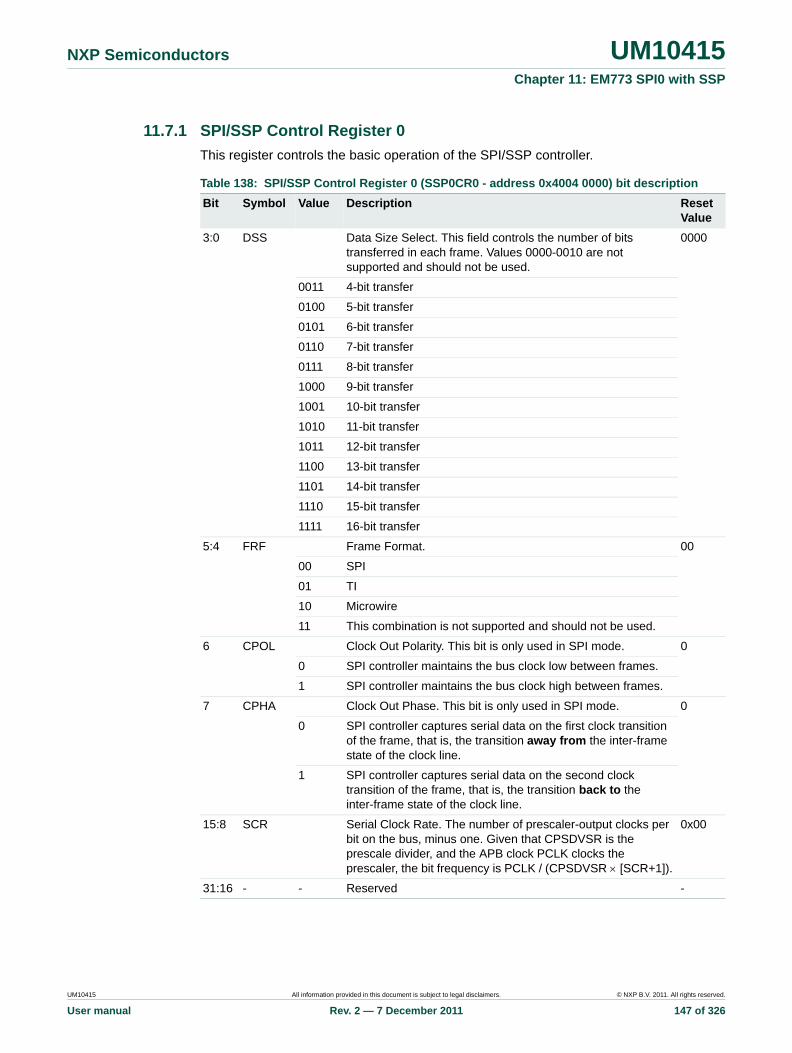
NXP Semiconductors UM10415Chapter 11: EM773 SPI0 with SSP
11.7.1 SPI/SSP Control Register 0
This register controls the basic operation of the SPI/SSP controller.
Table 138: SPI/SSP Control Register 0 (SSP0CR0 - address 0x4004 0000) bit description
Bit Symbol Value Description Reset Value
3:0 DSS Data Size Select. This field controls the number of bits transferred in each frame. Values 0000-0010 are not supported and should not be used.
0000
0011 4-bit transfer
0100 5-bit transfer
0101 6-bit transfer
0110 7-bit transfer
0111 8-bit transfer
1000 9-bit transfer
1001 10-bit transfer
1010 11-bit transfer
1011 12-bit transfer
1100 13-bit transfer
1101 14-bit transfer
1110 15-bit transfer
1111 16-bit transfer
5:4 FRF Frame Format. 00
00 SPI
01 TI
10 Microwire
11 This combination is not supported and should not be used.
6 CPOL Clock Out Polarity. This bit is only used in SPI mode. 0
0 SPI controller maintains the bus clock low between frames.
1 SPI controller maintains the bus clock high between frames.
7 CPHA Clock Out Phase. This bit is only used in SPI mode. 0
0 SPI controller captures serial data on the first clock transition of the frame, that is, the transition away from the inter-frame state of the clock line.
1 SPI controller captures serial data on the second clock transition of the frame, that is, the transition back to the inter-frame state of the clock line.
15:8 SCR Serial Clock Rate. The number of prescaler-output clocks per bit on the bus, minus one. Given that CPSDVSR is the prescale divider, and the APB clock PCLK clocks the prescaler, the bit frequency is PCLK / (CPSDVSR [SCR+1]).
0x00
31:16 - - Reserved -
UM10415 All information provided in this document is subject to legal disclaimers. © NXP B.V. 2011. All rights reserved.
User manual Rev. 2 — 7 December 2011 147 of 326
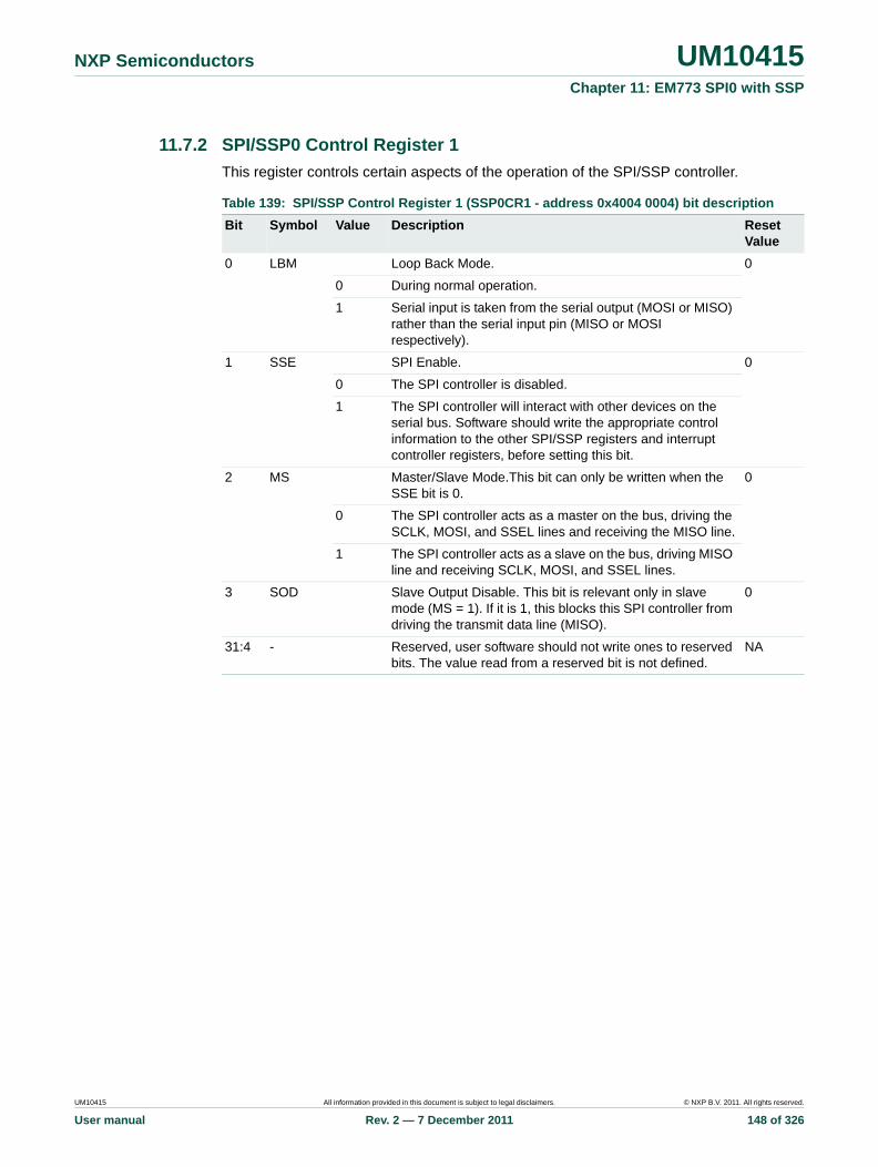
NXP Semiconductors UM10415Chapter 11: EM773 SPI0 with SSP
11.7.2 SPI/SSP0 Control Register 1
This register controls certain aspects of the operation of the SPI/SSP controller.
Table 139: SPI/SSP Control Register 1 (SSP0CR1 - address 0x4004 0004) bit description
Bit Symbol Value Description Reset Value
0 LBM Loop Back Mode. 0
0 During normal operation.
1 Serial input is taken from the serial output (MOSI or MISO) rather than the serial input pin (MISO or MOSI respectively).
1 SSE SPI Enable. 0
0 The SPI controller is disabled.
1 The SPI controller will interact with other devices on the serial bus. Software should write the appropriate control information to the other SPI/SSP registers and interrupt controller registers, before setting this bit.
2 MS Master/Slave Mode.This bit can only be written when the SSE bit is 0.
0
0 The SPI controller acts as a master on the bus, driving the SCLK, MOSI, and SSEL lines and receiving the MISO line.
1 The SPI controller acts as a slave on the bus, driving MISO line and receiving SCLK, MOSI, and SSEL lines.
3 SOD Slave Output Disable. This bit is relevant only in slave mode (MS = 1). If it is 1, this blocks this SPI controller from driving the transmit data line (MISO).
0
31:4 - Reserved, user software should not write ones to reserved bits. The value read from a reserved bit is not defined.
NA
UM10415 All information provided in this document is subject to legal disclaimers. © NXP B.V. 2011. All rights reserved.
User manual Rev. 2 — 7 December 2011 148 of 326
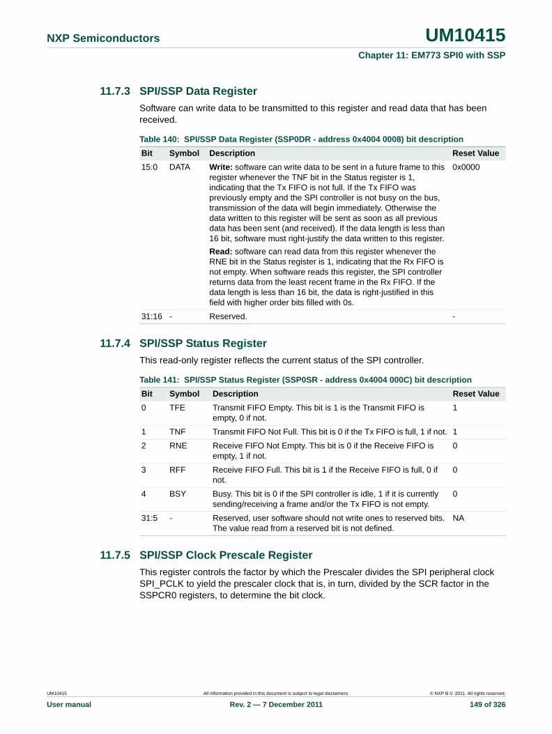
NXP Semiconductors UM10415Chapter 11: EM773 SPI0 with SSP
11.7.3 SPI/SSP Data Register
Software can write data to be transmitted to this register and read data that has been received.
11.7.4 SPI/SSP Status Register
This read-only register reflects the current status of the SPI controller.
11.7.5 SPI/SSP Clock Prescale Register
This register controls the factor by which the Prescaler divides the SPI peripheral clock SPI_PCLK to yield the prescaler clock that is, in turn, divided by the SCR factor in the SSPCR0 registers, to determine the bit clock.
Table 140: SPI/SSP Data Register (SSP0DR - address 0x4004 0008) bit description
Bit Symbol Description Reset Value
15:0 DATA Write: software can write data to be sent in a future frame to this register whenever the TNF bit in the Status register is 1, indicating that the Tx FIFO is not full. If the Tx FIFO was previously empty and the SPI controller is not busy on the bus, transmission of the data will begin immediately. Otherwise the data written to this register will be sent as soon as all previous data has been sent (and received). If the data length is less than 16 bit, software must right-justify the data written to this register.
Read: software can read data from this register whenever the RNE bit in the Status register is 1, indicating that the Rx FIFO is not empty. When software reads this register, the SPI controller returns data from the least recent frame in the Rx FIFO. If the data length is less than 16 bit, the data is right-justified in this field with higher order bits filled with 0s.
0x0000
31:16 - Reserved. -
Table 141: SPI/SSP Status Register (SSP0SR - address 0x4004 000C) bit description
Bit Symbol Description Reset Value
0 TFE Transmit FIFO Empty. This bit is 1 is the Transmit FIFO is empty, 0 if not.
1
1 TNF Transmit FIFO Not Full. This bit is 0 if the Tx FIFO is full, 1 if not. 1
2 RNE Receive FIFO Not Empty. This bit is 0 if the Receive FIFO is empty, 1 if not.
0
3 RFF Receive FIFO Full. This bit is 1 if the Receive FIFO is full, 0 if not.
0
4 BSY Busy. This bit is 0 if the SPI controller is idle, 1 if it is currently sending/receiving a frame and/or the Tx FIFO is not empty.
0
31:5 - Reserved, user software should not write ones to reserved bits. The value read from a reserved bit is not defined.
NA
UM10415 All information provided in this document is subject to legal disclaimers. © NXP B.V. 2011. All rights reserved.
User manual Rev. 2 — 7 December 2011 149 of 326
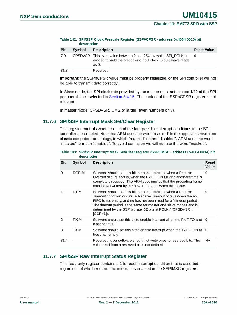
NXP Semiconductors UM10415Chapter 11: EM773 SPI0 with SSP
Important: the SSPnCPSR value must be properly initialized, or the SPI controller will not be able to transmit data correctly.
In Slave mode, the SPI clock rate provided by the master must not exceed 1/12 of the SPI peripheral clock selected in Section 3.4.15. The content of the SSPnCPSR register is not relevant.
In master mode, CPSDVSRmin = 2 or larger (even numbers only).
11.7.6 SPI/SSP Interrupt Mask Set/Clear Register
This register controls whether each of the four possible interrupt conditions in the SPI controller are enabled. Note that ARM uses the word “masked” in the opposite sense from classic computer terminology, in which “masked” meant “disabled”. ARM uses the word “masked” to mean “enabled”. To avoid confusion we will not use the word “masked”.
11.7.7 SPI/SSP Raw Interrupt Status Register
This read-only register contains a 1 for each interrupt condition that is asserted, regardless of whether or not the interrupt is enabled in the SSPIMSC registers.
Table 142: SPI/SSP Clock Prescale Register (SSP0CPSR - address 0x4004 0010) bit description
Bit Symbol Description Reset Value
7:0 CPSDVSR This even value between 2 and 254, by which SPI_PCLK is divided to yield the prescaler output clock. Bit 0 always reads as 0.
0
31:8 - Reserved. -
Table 143: SPI/SSP Interrupt Mask Set/Clear register (SSP0IMSC - address 0x4004 0014) bit description
Bit Symbol Description Reset Value
0 RORIM Software should set this bit to enable interrupt when a Receive Overrun occurs, that is, when the Rx FIFO is full and another frame is completely received. The ARM spec implies that the preceding frame data is overwritten by the new frame data when this occurs.
0
1 RTIM Software should set this bit to enable interrupt when a Receive Timeout condition occurs. A Receive Timeout occurs when the Rx FIFO is not empty, and no has not been read for a "timeout period". The timeout period is the same for master and slave modes and is determined by the SSP bit rate: 32 bits at PCLK / (CPSDVSR [SCR+1]).
0
2 RXIM Software should set this bit to enable interrupt when the Rx FIFO is at least half full.
0
3 TXIM Software should set this bit to enable interrupt when the Tx FIFO is at least half empty.
0
31:4 - Reserved, user software should not write ones to reserved bits. The value read from a reserved bit is not defined.
NA
UM10415 All information provided in this document is subject to legal disclaimers. © NXP B.V. 2011. All rights reserved.
User manual Rev. 2 — 7 December 2011 150 of 326
NXP Semiconductors UM10415Chapter 11: EM773 SPI0 with SSP
11.7.8 SPI/SSP Masked Interrupt Status Register
This read-only register contains a 1 for each interrupt condition that is asserted and enabled in the SSPIMSC registers. When an SPI interrupt occurs, the interrupt service routine should read this register to determine the cause(s) of the interrupt.
11.7.9 SPI/SSP Interrupt Clear Register
Software can write one or more one(s) to this write-only register, to clear the corresponding interrupt condition(s) in the SPI controller. Note that the other two interrupt conditions can be cleared by writing or reading the appropriate FIFO or disabled by clearing the corresponding bit in SSPIMSC registers.
Table 144: SPI/SSP Raw Interrupt Status register (SSP0RIS - address 0x4004 0018) bit description
Bit Symbol Description Reset Value
0 RORRIS This bit is 1 if another frame was completely received while the RxFIFO was full. The ARM spec implies that the preceding frame data is overwritten by the new frame data when this occurs.
0
1 RTRIS This bit is 1 if the Rx FIFO is not empty, and has not been read for a "timeout period". The timeout period is the same for master and slave modes and is determined by the SSP bit rate: 32 bits at PCLK / (CPSDVSR [SCR+1]).
0
2 RXRIS This bit is 1 if the Rx FIFO is at least half full. 0
3 TXRIS This bit is 1 if the Tx FIFO is at least half empty. 1
31:4 - Reserved, user software should not write ones to reserved bits. The value read from a reserved bit is not defined.
NA
Table 145: SPI/SSP Masked Interrupt Status register (SSP0MIS - address 0x4004 001C) bit description
Bit Symbol Description Reset Value
0 RORMIS This bit is 1 if another frame was completely received while the RxFIFO was full, and this interrupt is enabled.
0
1 RTMIS This bit is 1 if the Rx FIFO is not empty, has not been read for a "timeout period", and this interrupt is enabled. The timeout period is the same for master and slave modes and is determined by the SSP bit rate: 32 bits at PCLK / (CPSDVSR [SCR+1]).
0
2 RXMIS This bit is 1 if the Rx FIFO is at least half full, and this interrupt is enabled.
0
3 TXMIS This bit is 1 if the Tx FIFO is at least half empty, and this interrupt is enabled.
0
31:4 - Reserved, user software should not write ones to reserved bits. The value read from a reserved bit is not defined.
NA
UM10415 All information provided in this document is subject to legal disclaimers. © NXP B.V. 2011. All rights reserved.
User manual Rev. 2 — 7 December 2011 151 of 326

NXP Semiconductors UM10415Chapter 11: EM773 SPI0 with SSP
11.8 Functional description
11.8.1 Texas Instruments synchronous serial frame format
Figure 31 shows the 4-wire Texas Instruments synchronous serial frame format supported by the SPI module.
For device configured as a master in this mode, CLK and FS are forced LOW, and the transmit data line DX is in 3-state mode whenever the SSP is idle. Once the bottom entry of the transmit FIFO contains data, FS is pulsed HIGH for one CLK period. The value to be transmitted is also transferred from the transmit FIFO to the serial shift register of the transmit logic. On the next rising edge of CLK, the MSB of the 4-bit to 16-bit data frame is shifted out on the DX pin. Likewise, the MSB of the received data is shifted onto the DR pin by the off-chip serial slave device.
Table 146: SPI/SSP interrupt Clear Register (SSP0ICR - address 0x4004 0020) bit description
Bit Symbol Description Reset Value
0 RORIC Writing a 1 to this bit clears the “frame was received when RxFIFO was full” interrupt.
NA
1 RTIC Writing a 1 to this bit clears the Rx FIFO was not empty and has not been read for a timeout period interrupt. The timeout period is the same for master and slave modes and is determined by the SSP bit rate: 32 bits at PCLK / (CPSDVSR [SCR+1]).
NA
31:2 - Reserved, user software should not write ones to reserved bits. The value read from a reserved bit is not defined.
NA
a. Single frame transfer
b. Continuous/back-to-back frames transfer
Fig 31. Texas Instruments Synchronous Serial Frame Format: a) Single and b) Continuous/back-to-back Two Frames Transfer
CLK
FS
DX/DR
4 to 16 bits
MSB LSB
CLK
FS
DX/DR LSBMSB LSBMSB
4 to 16 bits 4 to 16 bits
UM10415 All information provided in this document is subject to legal disclaimers. © NXP B.V. 2011. All rights reserved.
User manual Rev. 2 — 7 December 2011 152 of 326

NXP Semiconductors UM10415Chapter 11: EM773 SPI0 with SSP
Both the SSP and the off-chip serial slave device then clock each data bit into their serial shifter on the falling edge of each CLK. The received data is transferred from the serial shifter to the receive FIFO on the first rising edge of CLK after the LSB has been latched.
11.8.2 SPI frame format
The SPI interface is a four-wire interface where the SSEL signal behaves as a slave select. The main feature of the SPI format is that the inactive state and phase of the SCK signal are programmable through the CPOL and CPHA bits within the SSPCR0 control register.
11.8.2.1 Clock Polarity (CPOL) and Phase (CPHA) control
When the CPOL clock polarity control bit is LOW, it produces a steady state low value on the SCK pin. If the CPOL clock polarity control bit is HIGH, a steady state high value is placed on the CLK pin when data is not being transferred.
The CPHA control bit selects the clock edge that captures data and allows it to change state. It has the most impact on the first bit transmitted by either allowing or not allowing a clock transition before the first data capture edge. When the CPHA phase control bit is LOW, data is captured on the first clock edge transition. If the CPHA clock phase control bit is HIGH, data is captured on the second clock edge transition.
11.8.2.2 SPI format with CPOL=0,CPHA=0
Single and continuous transmission signal sequences for SPI format with CPOL = 0, CPHA = 0 are shown in Figure 32.
a. Single transfer with CPOL=0 and CPHA=0
b. Continuous transfer with CPOL=0 and CPHA=0
Fig 32. SPI frame format with CPOL=0 and CPHA=0 (a) Single and b) Continuous Transfer)
SCKSSEL
MOSIMSB LSB
QMSB LSB
4 to 16 bits
MISO
SCKSSEL
MOSI
MISO
4 to 16 bits 4 to 16 bits
MSB LSBMSB LSB
QMSB LSB QMSB LSB
UM10415 All information provided in this document is subject to legal disclaimers. © NXP B.V. 2011. All rights reserved.
User manual Rev. 2 — 7 December 2011 153 of 326
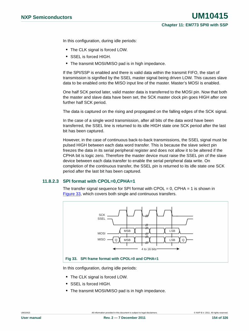
NXP Semiconductors UM10415Chapter 11: EM773 SPI0 with SSP
In this configuration, during idle periods:
• The CLK signal is forced LOW.
• SSEL is forced HIGH.
• The transmit MOSI/MISO pad is in high impedance.
If the SPI/SSP is enabled and there is valid data within the transmit FIFO, the start of transmission is signified by the SSEL master signal being driven LOW. This causes slave data to be enabled onto the MISO input line of the master. Master’s MOSI is enabled.
One half SCK period later, valid master data is transferred to the MOSI pin. Now that both the master and slave data have been set, the SCK master clock pin goes HIGH after one further half SCK period.
The data is captured on the rising and propagated on the falling edges of the SCK signal.
In the case of a single word transmission, after all bits of the data word have been transferred, the SSEL line is returned to its idle HIGH state one SCK period after the last bit has been captured.
However, in the case of continuous back-to-back transmissions, the SSEL signal must be pulsed HIGH between each data word transfer. This is because the slave select pin freezes the data in its serial peripheral register and does not allow it to be altered if the CPHA bit is logic zero. Therefore the master device must raise the SSEL pin of the slave device between each data transfer to enable the serial peripheral data write. On completion of the continuous transfer, the SSEL pin is returned to its idle state one SCK period after the last bit has been captured.
11.8.2.3 SPI format with CPOL=0,CPHA=1
The transfer signal sequence for SPI format with CPOL = 0, CPHA = 1 is shown in Figure 33, which covers both single and continuous transfers.
In this configuration, during idle periods:
• The CLK signal is forced LOW.
• SSEL is forced HIGH.
• The transmit MOSI/MISO pad is in high impedance.
Fig 33. SPI frame format with CPOL=0 and CPHA=1
SCKSSEL
MOSI
Q
4 to 16 bits
MISO Q MSB
MSB LSB
LSB
UM10415 All information provided in this document is subject to legal disclaimers. © NXP B.V. 2011. All rights reserved.
User manual Rev. 2 — 7 December 2011 154 of 326

NXP Semiconductors UM10415Chapter 11: EM773 SPI0 with SSP
If the SPI/SSP is enabled and there is valid data within the transmit FIFO, the start of transmission is signified by the SSEL master signal being driven LOW. Master’s MOSI pin is enabled. After a further one half SCK period, both master and slave valid data is enabled onto their respective transmission lines. At the same time, the SCK is enabled with a rising edge transition.
Data is then captured on the falling edges and propagated on the rising edges of the SCK signal.
In the case of a single word transfer, after all bits have been transferred, the SSEL line is returned to its idle HIGH state one SCK period after the last bit has been captured.
For continuous back-to-back transfers, the SSEL pin is held LOW between successive data words and termination is the same as that of the single word transfer.
11.8.2.4 SPI format with CPOL = 1,CPHA = 0
Single and continuous transmission signal sequences for SPI format with CPOL=1, CPHA=0 are shown in Figure 34.
In this configuration, during idle periods:
• The CLK signal is forced HIGH.
• SSEL is forced HIGH.
• The transmit MOSI/MISO pad is in high impedance.
a. Single transfer with CPOL=1 and CPHA=0
b. Continuous transfer with CPOL=1 and CPHA=0
Fig 34. SPI frame format with CPOL = 1 and CPHA = 0 (a) Single and b) Continuous Transfer)
SCK
SSEL
QMSB LSB
4 to 16 bits
MISO
MOSIMSB LSB
SCK
SSEL
MOSI
MISO
4 to 16 bits 4 to 16 bits
MSB LSBMSB LSB
QMSB LSB QMSB LSB
UM10415 All information provided in this document is subject to legal disclaimers. © NXP B.V. 2011. All rights reserved.
User manual Rev. 2 — 7 December 2011 155 of 326

NXP Semiconductors UM10415Chapter 11: EM773 SPI0 with SSP
If the SPI/SSP is enabled and there is valid data within the transmit FIFO, the start of transmission is signified by the SSEL master signal being driven LOW, which causes slave data to be immediately transferred onto the MISO line of the master. Master’s MOSI pin is enabled.
One half period later, valid master data is transferred to the MOSI line. Now that both the master and slave data have been set, the SCK master clock pin becomes LOW after one further half SCK period. This means that data is captured on the falling edges and be propagated on the rising edges of the SCK signal.
In the case of a single word transmission, after all bits of the data word are transferred, the SSEL line is returned to its idle HIGH state one SCK period after the last bit has been captured.
However, in the case of continuous back-to-back transmissions, the SSEL signal must be pulsed HIGH between each data word transfer. This is because the slave select pin freezes the data in its serial peripheral register and does not allow it to be altered if the CPHA bit is logic zero. Therefore the master device must raise the SSEL pin of the slave device between each data transfer to enable the serial peripheral data write. On completion of the continuous transfer, the SSEL pin is returned to its idle state one SCK period after the last bit has been captured.
11.8.2.5 SPI format with CPOL = 1,CPHA = 1
The transfer signal sequence for SPI format with CPOL = 1, CPHA = 1 is shown in Figure 35, which covers both single and continuous transfers.
In this configuration, during idle periods:
• The CLK signal is forced HIGH.
• SSEL is forced HIGH.
• The transmit MOSI/MISO pad is in high impedance.
If the SPI/SSP is enabled and there is valid data within the transmit FIFO, the start of transmission is signified by the SSEL master signal being driven LOW. Master’s MOSI is enabled. After a further one half SCK period, both master and slave data are enabled onto their respective transmission lines. At the same time, the SCK is enabled with a falling edge transition. Data is then captured on the rising edges and propagated on the falling edges of the SCK signal.
Fig 35. SPI Frame Format with CPOL = 1 and CPHA = 1
SCK
SSEL
MOSI
Q
4 to 16 bits
MISO Q MSB
MSB LSB
LSB
UM10415 All information provided in this document is subject to legal disclaimers. © NXP B.V. 2011. All rights reserved.
User manual Rev. 2 — 7 December 2011 156 of 326

NXP Semiconductors UM10415Chapter 11: EM773 SPI0 with SSP
After all bits have been transferred, in the case of a single word transmission, the SSEL line is returned to its idle HIGH state one SCK period after the last bit has been captured. For continuous back-to-back transmissions, the SSEL pins remains in its active LOW state, until the final bit of the last word has been captured, and then returns to its idle state as described above. In general, for continuous back-to-back transfers the SSEL pin is held LOW between successive data words and termination is the same as that of the single word transfer.
11.8.3 Semiconductor Microwire frame format
Figure 36 shows the Microwire frame format for a single frame. Figure 37 shows the same format when back-to-back frames are transmitted.
Microwire format is very similar to SPI format, except that transmission is half-duplex instead of full-duplex, using a master-slave message passing technique. Each serial transmission begins with an 8-bit control word that is transmitted from the SPI/SSP to the off-chip slave device. During this transmission, no incoming data is received by the SPI/SSP. After the message has been sent, the off-chip slave decodes it and, after waiting one serial clock after the last bit of the 8-bit control message has been sent, responds with the required data. The returned data is 4 to 16 bit in length, making the total frame length anywhere from 13 to 25 bits.
In this configuration, during idle periods:
• The SK signal is forced LOW.
• CS is forced HIGH.
• The transmit data line SO is arbitrarily forced LOW.
Fig 36. Microwire frame format (single transfer)
Fig 37. Microwire frame format (continuos transfers)
SKCS
SO
4 to 16 bitsof output data
SI 8-bit control
MSB LSB
0 MSB LSB
SK
CS
SO
SI
MSB LSB
4 to 16 bitsof output data
8-bit control
4 to 16 bitsof output data
MSB LSB0 MSB LSB
LSB
UM10415 All information provided in this document is subject to legal disclaimers. © NXP B.V. 2011. All rights reserved.
User manual Rev. 2 — 7 December 2011 157 of 326

NXP Semiconductors UM10415Chapter 11: EM773 SPI0 with SSP
A transmission is triggered by writing a control byte to the transmit FIFO.The falling edge of CS causes the value contained in the bottom entry of the transmit FIFO to be transferred to the serial shift register of the transmit logic, and the MSB of the 8-bit control frame to be shifted out onto the SO pin. CS remains LOW for the duration of the frame transmission. The SI pin remains tristated during this transmission.
The off-chip serial slave device latches each control bit into its serial shifter on the rising edge of each SK. After the last bit is latched by the slave device, the control byte is decoded during a one clock wait-state, and the slave responds by transmitting data back to the SPI/SSP. Each bit is driven onto SI line on the falling edge of SK. The SPI/SSP in turn latches each bit on the rising edge of SK. At the end of the frame, for single transfers, the CS signal is pulled HIGH one clock period after the last bit has been latched in the receive serial shifter, that causes the data to be transferred to the receive FIFO.
Note: The off-chip slave device can tristate the receive line either on the falling edge of SK after the LSB has been latched by the receive shiftier, or when the CS pin goes HIGH.
For continuous transfers, data transmission begins and ends in the same manner as a single transfer. However, the CS line is continuously asserted (held LOW) and transmission of data occurs back to back. The control byte of the next frame follows directly after the LSB of the received data from the current frame. Each of the received values is transferred from the receive shifter on the falling edge SK, after the LSB of the frame has been latched into the SPI/SSP.
11.8.3.1 Setup and hold time requirements on CS with respect to SK in Microwire mode
In the Microwire mode, the SPI/SSP slave samples the first bit of receive data on the rising edge of SK after CS has gone LOW. Masters that drive a free-running SK must ensure that the CS signal has sufficient setup and hold margins with respect to the rising edge of SK.
Figure 38 illustrates these setup and hold time requirements. With respect to the SK rising edge on which the first bit of receive data is to be sampled by the SPI/SSP slave, CS must have a setup of at least two times the period of SK on which the SPI/SSP operates. With respect to the SK rising edge previous to this edge, CS must have a hold of at least one SK period.
Fig 38. Microwire frame format setup and hold details
SKCS
SI
tHOLD= tSK
tSETUP=2*tSK
UM10415 All information provided in this document is subject to legal disclaimers. © NXP B.V. 2011. All rights reserved.
User manual Rev. 2 — 7 December 2011 158 of 326

12.1 How to read this chapter
The 16-bit timer block is identical for all EM773 parts.
12.2 Basic configuration
The CT16B0 is configured using the following registers:
1. Pins: The CT16B0 pins must be configured in the IOCONFIG register block (Section 6.4.1).
2. Power and peripheral clock: In the SYSAHBCLKCTRL register, set bit 7 and bit 8 (Table 17).
12.3 Features
• One 16-bit counter/timer with a programmable 16-bit prescaler.
• Counter or timer operation.
• One 16-bit capture channel that can take a snapshot of the timer value when an input signal transitions. A capture event may also optionally generate an interrupt.
• Four 16-bit match registers that allow:
– Continuous operation with optional interrupt generation on match.
– Stop timer on match with optional interrupt generation.
– Reset timer on match with optional interrupt generation.
• Up to three (CT16B0) external outputs corresponding to match registers with the following capabilities:
– Set LOW on match.
– Set HIGH on match.
– Toggle on match.
– Do nothing on match.
• For each timer, up to four match registers can be configured as PWM allowing to use up to three match outputs as single edge controlled PWM outputs.
12.4 Applications
• Interval timer for counting internal events
• Pulse Width Demodulator via capture input
• Free-running timer
• Pulse Width Modulator via match outputs
UM10415Chapter 12: EM773 16-bit counter/timer (CT16B0)Rev. 2 — 7 December 2011 User manual
UM10415 All information provided in this document is subject to legal disclaimers. © NXP B.V. 2011. All rights reserved.
User manual Rev. 2 — 7 December 2011 159 of 326
NXP Semiconductors UM10415Chapter 12: EM773 16-bit counter/timer (CT16B0)
12.5 Description
Each Counter/timer is designed to count cycles of the peripheral clock (PCLK) or an externally supplied clock and can optionally generate interrupts or perform other actions at specified timer values based on four match registers. Each counter/timer also includes one capture input to trap the timer value when an input signal transitions, optionally generating an interrupt.
In PWM mode, three match registers on CT16B0 can be used to provide a single-edge controlled PWM output on the match output pins. It is recommended to use the match registers that are not pinned out to control the PWM cycle length.
12.6 Pin description
Table 147 gives a brief summary of each of the counter/timer related pins.
12.7 Clocking and power control
The peripheral clocks (PCLK) to the 16-bit timers are provided by the system clock (see Figure 3). These clocks can be disabled through bit 7 and 8 in the AHBCLKCTRL register (Table 17) for power savings.
12.8 Register description
The 16-bit counter/timer0 contains the registers shown in Table 148. More detailed descriptions follow.
Table 147. Counter/timer pin description
Pin Type Description
CT16B0_CAP0 Input Capture Signal: A transition on a capture pin can be configured to load the Capture Register with the value in the counter/timer and optionally generate an interrupt.
Counter/Timer block can select a capture signal as a clock source instead of the PCLK derived clock. For more details see Section 12.8.11.
CT16B0_MAT[2:0] Output External Match Outputs of CT16B0:When a match register of CT16B0 (MR3:0) equals the timer counter (TC), this output can either toggle, go LOW, go HIGH, or do nothing. The External Match Register (EMR) and the PWM Control Register (PWMCON) control the functionality of this output.
UM10415 All information provided in this document is subject to legal disclaimers. © NXP B.V. 2011. All rights reserved.
User manual Rev. 2 — 7 December 2011 160 of 326

NXP Semiconductors UM10415Chapter 12: EM773 16-bit counter/timer (CT16B0)
[1] Reset value reflects the data stored in used bits only. It does not include reserved bits content.
12.8.1 Interrupt Register (TMR16B0IR)
The Interrupt Register (IR) consists of four bits for the match interrupts and one bit for the capture interrupt. If an interrupt is generated then the corresponding bit in the IR will be HIGH. Otherwise, the bit will be LOW. Writing a logic one to the corresponding IR bit will reset the interrupt. Writing a zero has no effect.
Table 148. Register overview: 16-bit counter/timer 0 CT16B0 (base address 0x4000 C000)
Name Access Address offset
Description Reset value[1]
TMR16B0IR R/W 0x000 Interrupt Register (IR). The IR can be written to clear interrupts. The IR can be read to identify which of five possible interrupt sources are pending.
0
TMR16B0TCR R/W 0x004 Timer Control Register (TCR). The TCR is used to control the Timer Counter functions. The Timer Counter can be disabled or reset through the TCR.
0
TMR16B0TC R/W 0x008 Timer Counter (TC). The 16-bit TC is incremented every PR+1 cycles of PCLK. The TC is controlled through the TCR.
0
TMR16B0PR R/W 0x00C Prescale Register (PR). When the Prescale Counter (below) is equal to this value, the next clock increments the TC and clears the PC.
0
TMR16B0PC R/W 0x010 Prescale Counter (PC). The 16-bit PC is a counter which is incremented to the value stored in PR. When the value in PR is reached, the TC is incremented and the PC is cleared. The PC is observable and controllable through the bus interface.
0
TMR16B0MCR R/W 0x014 Match Control Register (MCR). The MCR is used to control if an interrupt is generated and if the TC is reset when a Match occurs.
0
TMR16B0MR0 R/W 0x018 Match Register 0 (MR0). MR0 can be enabled through the MCR to reset the TC, stop both the TC and PC, and/or generate an interrupt every time MR0 matches the TC.
0
TMR16B0MR1 R/W 0x01C Match Register 1 (MR1). See MR0 description. 0
TMR16B0MR2 R/W 0x020 Match Register 2 (MR2). See MR0 description. 0
TMR16B0MR3 R/W 0x024 Match Register 3 (MR3). See MR0 description. 0
TMR16B0CCR R/W 0x028 Capture Control Register (CCR). The CCR controls which edges of the capture inputs are used to load the Capture Registers and whether or not an interrupt is generated when a capture takes place.
0
TMR16B0CR0 RO 0x02C Capture Register 0 (CR0). CR0 is loaded with the value of TC when there is an event on the CT16B0_CAP0 input.
0
TMR16B0EMR R/W 0x03C External Match Register (EMR). The EMR controls the match function and the external match pins CT16B0_MAT[2:0].
0
- - 0x040 - 0x06C
reserved -
TMR16B0CTCR R/W 0x070 Count Control Register (CTCR). The CTCR selects between Timer and Counter mode, and in Counter mode selects the signal and edge(s) for counting.
0
TMR16B0PWMC R/W 0x074 PWM Control Register (PWMCON). The PWMCON enables PWM mode for the external match pins CT16B0_MAT[2:0].
0
UM10415 All information provided in this document is subject to legal disclaimers. © NXP B.V. 2011. All rights reserved.
User manual Rev. 2 — 7 December 2011 161 of 326

NXP Semiconductors UM10415Chapter 12: EM773 16-bit counter/timer (CT16B0)
12.8.2 Timer Control Register (TMR16B0TCR)
The Timer Control Register (TCR) is used to control the operation of the counter/timer.
12.8.3 Timer Counter (TMR16B0TC - address 0x4000 C008)
The 16-bit Timer Counter is incremented when the Prescale Counter reaches its terminal count. Unless it is reset before reaching its upper limit, the TC will count up through the value 0x0000 FFFF and then wrap back to the value 0x0000 0000. This event does not cause an interrupt, but a Match register can be used to detect an overflow if needed.
12.8.4 Prescale Register (TMR16B0PR - address 0x4000 C00C)
The 16-bit Prescale Register specifies the maximum value for the Prescale Counter.
12.8.5 Prescale Counter register (TMR16B0PC - address 0x4000 C010)
The 16-bit Prescale Counter controls division of PCLK by some constant value before it is applied to the Timer Counter. This allows control of the relationship between the resolution of the timer and the maximum time before the timer overflows. The Prescale Counter is incremented on every PCLK. When it reaches the value stored in the Prescale Register, the Timer Counter is incremented, and the Prescale Counter is reset on the next PCLK. This causes the TC to increment on every PCLK when PR = 0, every 2 PCLKs when PR = 1, etc.
12.8.6 Match Control Register (TMR16B0MCR)
The Match Control Register is used to control what operations are performed when one of the Match Registers matches the Timer Counter. The function of each of the bits is shown in Table 151.
Table 149. Interrupt Register (TMR16B0IR - address 0x4000 C000) bit description
Bit Symbol Description Reset value
0 MR0 Interrupt Interrupt flag for match channel 0. 0
1 MR1 Interrupt Interrupt flag for match channel 1. 0
2 MR2 Interrupt Interrupt flag for match channel 2. 0
3 MR3 Interrupt Interrupt flag for match channel 3. 0
4 CR0 Interrupt Interrupt flag for capture channel 0 event. 0
31:5 - Reserved -
Table 150. Timer Control Register (TMR16B0TCR - address 0x4000 C004) bit description
Bit Symbol Description Reset value
0 Counter Enable When one, the Timer Counter and Prescale Counter are enabled for counting. When zero, the counters are disabled.
0
1 Counter Reset When one, the Timer Counter and the Prescale Counter are synchronously reset on the next positive edge of PCLK. The counters remain reset until TCR[1] is returned to zero.
0
31:2 - Reserved, user software should not write ones to reserved bits. The value read from a reserved bit is not defined.
NA
UM10415 All information provided in this document is subject to legal disclaimers. © NXP B.V. 2011. All rights reserved.
User manual Rev. 2 — 7 December 2011 162 of 326

NXP Semiconductors UM10415Chapter 12: EM773 16-bit counter/timer (CT16B0)
12.8.7 Match Registers (TMR16B0MR0/1/2/3 - addresses 0x4000 C018/1C/20/24)
The Match register values are continuously compared to the Timer Counter value. When the two values are equal, actions can be triggered automatically. The action possibilities are to generate an interrupt, reset the Timer Counter, or stop the timer. Actions are controlled by the settings in the MCR register.
Table 151. Match Control Register (TMR16B0MCR - address 0x4000 C014) bit description
Bit Symbol Value Description Reset value
0 MR0I 1 Interrupt on MR0: an interrupt is generated when MR0 matches the value in the TC. 0
0 This interrupt is disabled
1 MR0R 1 Reset on MR0: the TC will be reset if MR0 matches it. 0
0 Feature disabled.
2 MR0S 1 Stop on MR0: the TC and PC will be stopped and TCR[0] will be set to 0 if MR0 matches the TC.
0
0 Feature disabled.
3 MR1I 1 Interrupt on MR1: an interrupt is generated when MR1 matches the value in the TC. 0
0 This interrupt is disabled
4 MR1R 1 Reset on MR1: the TC will be reset if MR1 matches it. 0
0 Feature disabled.
5 MR1S 1 Stop on MR1: the TC and PC will be stopped and TCR[0] will be set to 0 if MR1 matches the TC.
0
0 Feature disabled.
6 MR2I 1 Interrupt on MR2: an interrupt is generated when MR2 matches the value in the TC. 0
0 This interrupt is disabled
7 MR2R 1 Reset on MR2: the TC will be reset if MR2 matches it. 0
0 Feature disabled.
8 MR2S 1 Stop on MR2: the TC and PC will be stopped and TCR[0] will be set to 0 if MR2 matches the TC.
0
0 Feature disabled.
9 MR3I 1 Interrupt on MR3: an interrupt is generated when MR3 matches the value in the TC. 0
0 This interrupt is disabled
10 MR3R 1 Reset on MR3: the TC will be reset if MR3 matches it. 0
0 Feature disabled.
11 MR3S 1 Stop on MR3: the TC and PC will be stopped and TCR[0] will be set to 0 if MR3 matches the TC.
0
0 Feature disabled.
31:12 - Reserved, user software should not write ones to reserved bits. The value read from a reserved bit is not defined.
NA
UM10415 All information provided in this document is subject to legal disclaimers. © NXP B.V. 2011. All rights reserved.
User manual Rev. 2 — 7 December 2011 163 of 326

NXP Semiconductors UM10415Chapter 12: EM773 16-bit counter/timer (CT16B0)
12.8.8 Capture Control Register (TMR16B0CCR)
The Capture Control Register is used to control whether the Capture Register is loaded with the value in the Counter/timer when the capture event occurs, and whether an interrupt is generated by the capture event. Setting both the rising and falling bits at the same time is a valid configuration, resulting in a capture event for both edges. In the description below, "n" represents the Timer number, 0.
12.8.9 Capture Register (CT16B0CR0 - address 0x4000 C02C)
Each Capture register is associated with a device pin and may be loaded with the counter/timer value when a specified event occurs on that pin. The settings in the Capture Control Register register determine whether the capture function is enabled, and whether a capture event happens on the rising edge of the associated pin, the falling edge, or on both edges.
12.8.10 External Match Register (TMR16B0EMR)
The External Match Register provides both control and status of the external match channels and external match pins CT16B0_MAT[2:0].
If the match outputs are configured as PWM output in the PWMCON registers (Section 12.8.12), the function of the external match registers is determined by the PWM rules (Section 12.8.13 “Rules for single edge controlled PWM outputs” on page 167).
Table 152. Capture Control Register (TMR16B0CCR - address 0x4000 C028) bit description
Bit Symbol Value Description Reset value
0 CAP0RE 1 Capture on CT16Bn_CAP0 rising edge: a sequence of 0 then 1 on CT16Bn_CAP0 will cause CR0 to be loaded with the contents of TC.
0
0 This feature is disabled.
1 CAP0FE 1 Capture on CT16Bn_CAP0 falling edge: a sequence of 1 then 0 on CT16Bn_CAP0 will cause CR0 to be loaded with the contents of TC.
0
0 This feature is disabled.
2 CAP0I1
Interrupt on CT16Bn_CAP0 event: a CR0 load due to a CT16Bn_CAP0 event will generate an interrupt.
0
0 This feature is disabled.
31:3 - - Reserved, user software should not write ones to reserved bits. The value read from a reserved bit is not defined.
NA
UM10415 All information provided in this document is subject to legal disclaimers. © NXP B.V. 2011. All rights reserved.
User manual Rev. 2 — 7 December 2011 164 of 326

NXP Semiconductors UM10415Chapter 12: EM773 16-bit counter/timer (CT16B0)
12.8.11 Count Control Register (TMR16B0CTCR)
The Count Control Register (CTCR) is used to select between Timer and Counter mode, and in Counter mode to select the pin and edge(s) for counting.
When Counter Mode is chosen as a mode of operation, the CAP input (selected by the CTCR bits 3:2) is sampled on every rising edge of the PCLK clock. After comparing two consecutive samples of this CAP input, one of the following four events is recognized:
Table 153. External Match Register (TMR16B0EMR - address 0x4000 C03C) bit description
Bit Symbol Description Reset value
0 EM0 External Match 0. This bit reflects the state of output CT16B0_MAT0, whether or not this output is connected to its pin. When a match occurs between the TC and MR0, this bit can either toggle, go LOW, go HIGH, or do nothing. Bits EMR[5:4] control the functionality of this output. This bit is driven to the CT16B0_MAT0 pins if the match function is selected in the IOCON registers (0 = LOW, 1 = HIGH).
0
1 EM1 External Match 1. This bit reflects the state of output CT16B0_MAT1, whether or not this output is connected to its pin. When a match occurs between the TC and MR1, this bit can either toggle, go LOW, go HIGH, or do nothing. Bits EMR[7:6] control the functionality of this output. This bit is driven to the CT16B0_MAT1 pins if the match function is selected in the IOCON registers (0 = LOW, 1 = HIGH).
0
2 EM2 External Match 2. This bit reflects the state of output match channel 2, whether or not this output is connected to its pin. When a match occurs between the TC and MR2, this bit can either toggle, go LOW, go HIGH, or do nothing. Bits EMR[9:8] control the functionality of this output. Note that on counter/timer 0 this match channel is not pinned out. This bit is driven to the CT16B0_MAT2 pin if the match function is selected in the IOCON registers (0 = LOW, 1 = HIGH).
0
3 EM3 External Match 3. This bit reflects the state of output of match channel 3. When a match occurs between the TC and MR3, this bit can either toggle, go LOW, go HIGH, or do nothing. Bits EMR[11:10] control the functionality of this output. There is no output pin available for this channel on the 16-bit timer.
0
5:4 EMC0 External Match Control 0. Determines the functionality of External Match 0. Table 154 shows the encoding of these bits.
00
7:6 EMC1 External Match Control 1. Determines the functionality of External Match 1. Table 154 shows the encoding of these bits.
00
9:8 EMC2 External Match Control 2. Determines the functionality of External Match 2. Table 154 shows the encoding of these bits.
00
11:10 EMC3 External Match Control 3. Determines the functionality of External Match 3. Table 154 shows the encoding of these bits.
00
31:12 - Reserved, user software should not write ones to reserved bits. The value read from a reserved bit is not defined.
NA
Table 154. External match control
EMR[11:10], EMR[9:8],EMR[7:6], or EMR[5:4]
Function
00 Do Nothing.
01 Clear the corresponding External Match bit/output to 0 (CT16Bn_MATm pin is LOW if pinned out).
10 Set the corresponding External Match bit/output to 1 (CT16Bn_MATm pin is HIGH if pinned out).
11 Toggle the corresponding External Match bit/output.
UM10415 All information provided in this document is subject to legal disclaimers. © NXP B.V. 2011. All rights reserved.
User manual Rev. 2 — 7 December 2011 165 of 326

NXP Semiconductors UM10415Chapter 12: EM773 16-bit counter/timer (CT16B0)
rising edge, falling edge, either of edges or no changes in the level of the selected CAP input. Only if the identified event occurs, and the event corresponds to the one selected by bits 1:0 in the CTCR register, will the Timer Counter register be incremented.
Effective processing of the externally supplied clock to the counter has some limitations. Since two successive rising edges of the PCLK clock are used to identify only one edge on the CAP selected input, the frequency of the CAP input can not exceed one half of the PCLK clock. Consequently, duration of the HIGH/LOW levels on the same CAP input in this case can not be shorter than 1/(2 PCLK).
12.8.12 PWM Control register (TMR16B0PWMC)
The PWM Control Register is used to configure the match outputs as PWM outputs. Each match output can be independently set to perform either as PWM output or as match output whose function is controlled by the External Match Register (EMR).
For timer 0, three single-edge controlled PWM outputs can be selected on the CT16B0_MAT[2:0] outputs. One additional match register determines the PWM cycle length. When a match occurs in any of the other match registers, the PWM output is set to HIGH. The timer is reset by the match register that is configured to set the PWM cycle length. When the timer is reset to zero, all currently HIGH match outputs configured as PWM outputs are cleared.
Table 155. Count Control Register (TMR16B0CTCR - address 0x4000 C070) bit description
Bit Symbol Value Description Reset value
1:0 Counter/Timer Mode
00
This field selects which rising PCLK edges can increment Timer’s Prescale Counter (PC), or clear PC and increment Timer Counter (TC).
Timer Mode: every rising PCLK edge
00
01 Counter Mode: TC is incremented on rising edges on the CAP input selected by bits 3:2.
10 Counter Mode: TC is incremented on falling edges on the CAP input selected by bits 3:2.
11 Counter Mode: TC is incremented on both edges on the CAP input selected by bits 3:2.
3:2 Count Input Select 00
In counter mode (when bits 1:0 in this register are not 00), these bits select which CAP pin is sampled for clocking:
CT16Bn_CAP0
00
01 Reserved.
10 Reserved.
Note: If Counter mode is selected in the CTCR register, bits 2:0 in the Capture Control Register (CCR) must be programmed as 000.
11 Reserved.
31:4 - - Reserved, user software should not write ones to reserved bits. The value read from a reserved bit is not defined.
NA
UM10415 All information provided in this document is subject to legal disclaimers. © NXP B.V. 2011. All rights reserved.
User manual Rev. 2 — 7 December 2011 166 of 326

NXP Semiconductors UM10415Chapter 12: EM773 16-bit counter/timer (CT16B0)
12.8.13 Rules for single edge controlled PWM outputs
1. All single edge controlled PWM outputs go LOW at the beginning of each PWM cycle (timer is set to zero) unless their match value is equal to zero.
2. Each PWM output will go HIGH when its match value is reached. If no match occurs (i.e. the match value is greater than the PWM cycle length), the PWM output remains continuously LOW.
3. If a match value larger than the PWM cycle length is written to the match register, and the PWM signal is HIGH already, then the PWM signal will be cleared on the next start of the next PWM cycle.
4. If a match register contains the same value as the timer reset value (the PWM cycle length), then the PWM output will be reset to LOW on the next clock tick. Therefore, the PWM output will always consist of a one clock tick wide positive pulse with a period determined by the PWM cycle length (i.e. the timer reload value).
5. If a match register is set to zero, then the PWM output will go to HIGH the first time the timer goes back to zero and will stay HIGH continuously.
Note: When the match outputs are selected to serve as PWM outputs, the timer reset (MRnR) and timer stop (MRnS) bits in the Match Control Register MCR must be set to 0 except for the match register setting the PWM cycle length. For this register, set the MRnR bit to 1 to enable the timer reset when the timer value matches the value of the corresponding match register.
Table 156. PWM Control Register (TMR16B0PWMC - address 0x4000 C074 and TMR16B1PWMC- address 0x4001 0074) bit description
Bit Symbol Description Reset value
0 PWM enable When one, PWM mode is enabled for CT16Bn_MAT0. When zero, CT16Bn_MAT0 is controlled by EM0.
0
1 PWM enable When one, PWM mode is enabled for CT16Bn_MAT1. When zero, CT16Bn_MAT1 is controlled by EM1.
0
2 PWM enable When one, PWM mode is enabled for match channel 2 or pin CT16B0_MAT2. When zero, match channel 2 or pin CT16B0_MAT2 is controlled by EM2. Match channel 2 is not pinned out on timer 1.
0
3 PWM enable When one, PWM mode is enabled for match channel 3match channel 3. When zero, match channel 3 match channel 3 is controlled by EM3.
Note: It is recommended to use match channel 3 to set the PWM cycle because it is not pinned out.
0
31:4 - Reserved, user software should not write ones to reserved bits. The value read from a reserved bit is not defined.
NA
UM10415 All information provided in this document is subject to legal disclaimers. © NXP B.V. 2011. All rights reserved.
User manual Rev. 2 — 7 December 2011 167 of 326

NXP Semiconductors UM10415Chapter 12: EM773 16-bit counter/timer (CT16B0)
12.9 Example timer operation
Figure 40 shows a timer configured to reset the count and generate an interrupt on match. The prescaler is set to 2 and the match register set to 6. At the end of the timer cycle where the match occurs, the timer count is reset. This gives a full length cycle to the match value. The interrupt indicating that a match occurred is generated in the next clock after the timer reached the match value.
Figure 41 shows a timer configured to stop and generate an interrupt on match. The prescaler is again set to 2 and the match register set to 6. In the next clock after the timer reaches the match value, the timer enable bit in TCR is cleared, and the interrupt indicating that a match occurred is generated.
Fig 39. Sample PWM waveforms with a PWM cycle length of 100 (selected by MR3) and MAT3:0 enabled as PWM outputs by the PWCON register.
100(counter is reset)
0 41 65
PWM0/MAT0
PWM1/MAT1
PWM2/MAT2 MR2 = 100
MR1 = 41
MR0 = 65
Fig 40. A timer cycle in which PR=2, MRx=6, and both interrupt and reset on match are enabled
PCLK
prescalecounter
interrupt
timercounter
timer counterreset
2222 0 0 0 01 1 1 1
4 5 6 0 1
Fig 41. A timer cycle in which PR=2, MRx=6, and both interrupt and stop on match are enabled
PCLK
prescale counter
interrupt
timer counter
TCR[0](counter enable)
22 0 01
4 5 6
1 0
UM10415 All information provided in this document is subject to legal disclaimers. © NXP B.V. 2011. All rights reserved.
User manual Rev. 2 — 7 December 2011 168 of 326

NXP Semiconductors UM10415Chapter 12: EM773 16-bit counter/timer (CT16B0)
12.10 Architecture
The block diagram for counter/timer0 and counter/timer1 is shown in Figure 42.
Fig 42. 16-bit counter/timer block diagram
reset MAXVAL
TIMER CONTROL REGISTER PRESCALE REGISTER
PRESCALE COUNTERPCLK
enable
CAPTURE REGISTER 0
MATCH REGISTER 3
MATCH REGISTER 2
MATCH REGISTER 1
MATCH REGISTER 0
CAPTURE CONTROL REGISTER
CONTROL
TIMER COUNTERCSN
TCI
CE
=
=
=
=
INTERRUPT REGISTER
EXTERNAL MATCH REGISTER
MATCH CONTROL REGISTER
MATn[2:0]
INTERRUPT
CAP0
STOP ON MATCH
RESET ON MATCH
LOAD[3:0]
UM10415 All information provided in this document is subject to legal disclaimers. © NXP B.V. 2011. All rights reserved.
User manual Rev. 2 — 7 December 2011 169 of 326

13.1 How to read this chapter
The 32-bit timer blocks are identical for all EM773 parts.
13.2 Basic configuration
The CT32B0/1 are configured using the following registers:
1. Pins: The CT32B0/1 pins must be configured in the IOCONFIG register block (Section 6.4.1).
2. Power and peripheral clock: In the SYSAHBCLKCTRL register, set bit 9 and bit 10 (Table 17).
13.3 Features
• Two 32-bit counter/timers with a programmable 32-bit prescaler.
• Counter or Timer operation.
• One 32-bit capture channel that can take a snapshot of the timer value when an input signal transitions. A capture event may also optionally generate an interrupt.
• Four 32-bit match registers that allow:
– Continuous operation with optional interrupt generation on match.
– Stop timer on match with optional interrupt generation.
– Reset timer on match with optional interrupt generation.
• Four external outputs corresponding to match registers with the following capabilities:
– Set LOW on match.
– Set HIGH on match.
– Toggle on match.
– Do nothing on match.
• For each timer, up to four match registers can be configured as PWM allowing to use up to three match outputs as single edge controlled PWM outputs.
13.4 Applications
• Interval timer for counting internal events
• Pulse Width Demodulator via capture input
• Free running timer
• Pulse Width Modulator via match outputs
UM10415Chapter 13: EM773 32-bit counter/timers (CT32B0/1)Rev. 2 — 7 December 2011 User manual
UM10415 All information provided in this document is subject to legal disclaimers. © NXP B.V. 2011. All rights reserved.
User manual Rev. 2 — 7 December 2011 170 of 326

NXP Semiconductors UM10415Chapter 13: EM773 32-bit counter/timers (CT32B0/1)
13.5 Description
Each Counter/timer is designed to count cycles of the peripheral clock (PCLK) or an externally supplied clock and can optionally generate interrupts or perform other actions at specified timer values based on four match registers. Each counter/timer also includes one capture input to trap the timer value when an input signal transitions, optionally generating an interrupt.
In PWM mode, three match registers can be used to provide a single-edge controlled PWM output on the match output pins. One match register is used to control the PWM cycle length.
Remark: 32-bit counter/timer0 (CT32B0) and 32-bit counter/timer1 (CT32B1) are functionally identical except for the peripheral base address.
13.6 Pin description
Table 157 gives a brief summary of each of the counter/timer related pins.
13.7 Clocking and power control
The peripheral clocks (PCLK) to the 32-bit timers are provided by the system clock (see Figure 3). These clocks can be disabled through bits 9 and 10 in the AHBCLKCTRL register (Table 17) for power savings.
13.8 Register description
32-bit counter/timer0 contains the registers shown in Table 158 and 32-bit counter/timer1 contains the registers shown in Table 159. More detailed descriptions follow.
Table 157. Counter/timer pin description
Pin Type Description
CT32B0_CAP0 Input Capture Signals:A transition on a capture pin can be configured to load one of the Capture Registers with the value in the Timer Counter and optionally generate an interrupt.
The counter/timer block can select a capture signal as a clock source instead of the PCLK derived clock. For more details see Section 13.8.11 “Count Control Register (TMR32B0CTCR and TMR32B1TCR)” on page 177.
CT32B0_MAT[2:0]CT32B1_MAT[3:0]
Output External Match Output of CT32B0/1:When a match register TMR32B0/1MR3:0 equals the timer counter (TC), this output can either toggle, go LOW, go HIGH, or do nothing. The External Match Register (EMR) and the PWM Control register (PWMCON) control the functionality of this output.
UM10415 All information provided in this document is subject to legal disclaimers. © NXP B.V. 2011. All rights reserved.
User manual Rev. 2 — 7 December 2011 171 of 326

NXP Semiconductors UM10415Chapter 13: EM773 32-bit counter/timers (CT32B0/1)
[1] Reset value reflects the data stored in used bits only. It does not include reserved bits content.
Table 158. Register overview: 32-bit counter/timer 0 CT32B0 (base address 0x4001 4000)
Name Access Address offset
Description Reset value[1]
TMR32B0IR R/W 0x000 Interrupt Register (IR). The IR can be written to clear interrupts. The IR can be read to identify which of five possible interrupt sources are pending.
0
TMR32B0TCR R/W 0x004 Timer Control Register (TCR). The TCR is used to control the Timer Counter functions. The Timer Counter can be disabled or reset through the TCR.
0
TMR32B0TC R/W 0x008 Timer Counter (TC). The 32-bit TC is incremented every PR+1 cycles of PCLK. The TC is controlled through the TCR.
0
TMR32B0PR R/W 0x00C Prescale Register (PR). When the Prescale Counter (below) is equal to this value, the next clock increments the TC and clears the PC.
0
TMR32B0PC R/W 0x010 Prescale Counter (PC). The 32-bit PC is a counter which is incremented to the value stored in PR. When the value in PR is reached, the TC is incremented and the PC is cleared. The PC is observable and controllable through the bus interface.
0
TMR32B0MCR R/W 0x014 Match Control Register (MCR). The MCR is used to control if an interrupt is generated and if the TC is reset when a Match occurs.
0
TMR32B0MR0 R/W 0x018 Match Register 0 (MR0). MR0 can be enabled through the MCR to reset the TC, stop both the TC and PC, and/or generate an interrupt every time MR0 matches the TC.
0
TMR32B0MR1 R/W 0x01C Match Register 1 (MR1). See MR0 description. 0
TMR32B0MR2 R/W 0x020 Match Register 2 (MR2). See MR0 description. 0
TMR32B0MR3 R/W 0x024 Match Register 3 (MR3). See MR0 description. 0
TMR32B0CCR R/W 0x028 Capture Control Register (CCR). The CCR controls which edges of the capture inputs are used to load the Capture Registers and whether or not an interrupt is generated when a capture takes place.
0
TMR32B0CR0 RO 0x02C Capture Register 0 (CR0). CR0 is loaded with the value of TC when there is an event on the CT32B0_CAP0 input.
0
TMR32B0EMR R/W 0x03C External Match Register (EMR). The EMR controls the match function and the external match pins CT32B0_MAT[2:0].
0
- - 0x040 - 0x06C
reserved -
TMR32B0CTCR R/W 0x070 Count Control Register (CTCR). The CTCR selects between Timer and Counter mode, and in Counter mode selects the signal and edge(s) for counting.
0
TMR32B0PWMC R/W 0x074 PWM Control Register (PWMCON). The PWMCON enables PWM mode for the external match pins CT32B0_MAT[2:0].
0
UM10415 All information provided in this document is subject to legal disclaimers. © NXP B.V. 2011. All rights reserved.
User manual Rev. 2 — 7 December 2011 172 of 326

NXP Semiconductors UM10415Chapter 13: EM773 32-bit counter/timers (CT32B0/1)
[1] Reset value reflects the data stored in used bits only. It does not include reserved bits content.
13.8.1 Interrupt Register (TMR32B0IR and TMR32B1IR)
The Interrupt Register consists of four bits for the match interrupts and one bit for the capture interrupts. If an interrupt is generated then the corresponding bit in the IR will be HIGH. Otherwise, the bit will be LOW. Writing a logic one to the corresponding IR bit will reset the interrupt. Writing a zero has no effect.
Table 159. Register overview: 32-bit counter/timer 1 CT32B1 (base address 0x4001 8000)
Name Access Address offset
Description Reset value[1]
TMR32B1IR R/W 0x000 Interrupt Register (IR). The IR can be written to clear interrupts. The IR can be read to identify which of five possible interrupt sources are pending.
0
TMR32B1TCR R/W 0x004 Timer Control Register (TCR). The TCR is used to control the Timer Counter functions. The Timer Counter can be disabled or reset through the TCR.
0
TMR32B1TC R/W 0x008 Timer Counter (TC). The 32-bit TC is incremented every PR+1 cycles of PCLK. The TC is controlled through the TCR.
0
TMR32B1PR R/W 0x00C Prescale Register (PR). When the Prescale Counter (below) is equal to this value, the next clock increments the TC and clears the PC.
0
TMR32B1PC R/W 0x010 Prescale Counter (PC). The 32-bit PC is a counter which is incremented to the value stored in PR. When the value in PR is reached, the TC is incremented and the PC is cleared. The PC is observable and controllable through the bus interface.
0
TMR32B1MCR R/W 0x014 Match Control Register (MCR). The MCR is used to control if an interrupt is generated and if the TC is reset when a Match occurs.
0
TMR32B1MR0 R/W 0x018 Match Register 0 (MR0). MR0 can be enabled through the MCR to reset the TC, stop both the TC and PC, and/or generate an interrupt every time MR0 matches the TC.
0
TMR32B1MR1 R/W 0x01C Match Register 1 (MR1). See MR0 description. 0
TMR32B1MR2 R/W 0x020 Match Register 2 (MR2). See MR0 description. 0
TMR32B1MR3 R/W 0x024 Match Register 3 (MR3). See MR0 description. 0
TMR32B1EMR R/W 0x03C External Match Register (EMR). The EMR controls the match function and the external match pins CT32B1_MAT[3:0].
0
- - 0x040 - 0x06C
reserved -
TMR32B1CTCR R/W 0x070 Count Control Register (CTCR). The CTCR selects between Timer and Counter mode, and in Counter mode selects the signal and edge(s) for counting.
0
TMR32B1PWMC R/W 0x074 PWM Control Register (PWMCON). The PWMCON enables PWM mode for the external match pins CT32B1_MAT[3:0].
0
Table 160: Interrupt Register (TMR32B0IR - address 0x4001 4000 and TMR32B1IR - address 0x4001 8000) bit description
Bit Symbol Description Reset value
0 MR0 Interrupt Interrupt flag for match channel 0. 0
1 MR1 Interrupt Interrupt flag for match channel 1. 0
2 MR2 Interrupt Interrupt flag for match channel 2. 0
UM10415 All information provided in this document is subject to legal disclaimers. © NXP B.V. 2011. All rights reserved.
User manual Rev. 2 — 7 December 2011 173 of 326

NXP Semiconductors UM10415Chapter 13: EM773 32-bit counter/timers (CT32B0/1)
13.8.2 Timer Control Register (TMR32B0TCR and TMR32B1TCR)
The Timer Control Register (TCR) is used to control the operation of the counter/timer.
13.8.3 Timer Counter (TMR32B0TC - address 0x4001 4008 and TMR32B1TC - address 0x4001 8008)
The 32-bit Timer Counter is incremented when the Prescale Counter reaches its terminal count. Unless it is reset before reaching its upper limit, the TC will count up through the value 0xFFFF FFFF and then wrap back to the value 0x0000 0000. This event does not cause an interrupt, but a Match register can be used to detect an overflow if needed.
13.8.4 Prescale Register (TMR32B0PR - address 0x4001 400C and TMR32B1PR - address 0x4001 800C)
The 32-bit Prescale Register specifies the maximum value for the Prescale Counter.
13.8.5 Prescale Counter Register (TMR32B0PC - address 0x4001 4010 and TMR32B1PC - address 0x4001 8010)
The 32-bit Prescale Counter controls division of PCLK by some constant value before it is applied to the Timer Counter. This allows control of the relationship between the resolution of the timer and the maximum time before the timer overflows. The Prescale Counter is incremented on every PCLK. When it reaches the value stored in the Prescale Register, the Timer Counter is incremented, and the Prescale Counter is reset on the next PCLK. This causes the TC to increment on every PCLK when PR = 0, every 2 PCLKs when PR = 1, etc.
3 MR3 Interrupt Interrupt flag for match channel 3. 0
4 CR0 Interrupt Interrupt flag for capture channel 0 event. 0
31:5 - Reserved -
Table 160: Interrupt Register (TMR32B0IR - address 0x4001 4000 and TMR32B1IR - address 0x4001 8000) bit description
Bit Symbol Description Reset value
Table 161: Timer Control Register (TMR32B0TCR - address 0x4001 4004 and TMR32B1TCR - address 0x4001 8004) bit description
Bit Symbol Description Reset value
0 Counter Enable When one, the Timer Counter and Prescale Counter are enabled for counting. When zero, the counters are disabled.
0
1 Counter Reset When one, the Timer Counter and the Prescale Counter are synchronously reset on the next positive edge of PCLK. The counters remain reset until TCR[1] is returned to zero.
0
31:2 - Reserved, user software should not write ones to reserved bits. The value read from a reserved bit is not defined.
NA
UM10415 All information provided in this document is subject to legal disclaimers. © NXP B.V. 2011. All rights reserved.
User manual Rev. 2 — 7 December 2011 174 of 326

NXP Semiconductors UM10415Chapter 13: EM773 32-bit counter/timers (CT32B0/1)
13.8.6 Match Control Register (TMR32B0MCR and TMR32B1MCR)
The Match Control Register is used to control what operations are performed when one of the Match Registers matches the Timer Counter. The function of each of the bits is shown in Table 162.
Table 162: Match Control Register (TMR32B0MCR - address 0x4001 4014 and TMR32B1MCR - address 0x4001 8014) bit description
Bit Symbol Value Description Reset value
0 MR0I 1 Interrupt on MR0: an interrupt is generated when MR0 matches the value in the TC. 0
0 This interrupt is disabled
1 MR0R 1 Reset on MR0: the TC will be reset if MR0 matches it. 0
0 Feature disabled.
2 MR0S 1 Stop on MR0: the TC and PC will be stopped and TCR[0] will be set to 0 if MR0 matches the TC.
0
0 Feature disabled.
3 MR1I 1 Interrupt on MR1: an interrupt is generated when MR1 matches the value in the TC. 0
0 This interrupt is disabled
4 MR1R 1 Reset on MR1: the TC will be reset if MR1 matches it. 0
0 Feature disabled.
5 MR1S 1 Stop on MR1: the TC and PC will be stopped and TCR[0] will be set to 0 if MR1 matches the TC.
0
0 Feature disabled.
6 MR2I 1 Interrupt on MR2: an interrupt is generated when MR2 matches the value in the TC. 0
0 This interrupt is disabled
7 MR2R 1 Reset on MR2: the TC will be reset if MR2 matches it. 0
0 Feature disabled.
8 MR2S 1 Stop on MR2: the TC and PC will be stopped and TCR[0] will be set to 0 if MR2 matches the TC.
0
0 Feature disabled.
9 MR3I 1 Interrupt on MR3: an interrupt is generated when MR3 matches the value in the TC. 0
0 This interrupt is disabled
10 MR3R 1 Reset on MR3: the TC will be reset if MR3 matches it. 0
0 Feature disabled.
11 MR3S 1 Stop on MR3: the TC and PC will be stopped and TCR[0] will be set to 0 if MR3 matches the TC.
0
0 Feature disabled.
31:12 - Reserved, user software should not write ones to reserved bits. The value read from a reserved bit is not defined.
NA
UM10415 All information provided in this document is subject to legal disclaimers. © NXP B.V. 2011. All rights reserved.
User manual Rev. 2 — 7 December 2011 175 of 326

NXP Semiconductors UM10415Chapter 13: EM773 32-bit counter/timers (CT32B0/1)
13.8.7 Match Registers (TMR32B0MR0/1/2/3 - addresses 0x4001 4018/1C/20/24 and TMR32B1MR0/1/2/3 addresses 0x4001 8018/1C/20/24)
The Match register values are continuously compared to the Timer Counter value. When the two values are equal, actions can be triggered automatically. The action possibilities are to generate an interrupt, reset the Timer Counter, or stop the timer. Actions are controlled by the settings in the MCR register.
13.8.8 Capture Control Register (TMR32B0CCR)
The Capture Control Register is used to control whether the Capture Register is loaded with the value in the Timer Counter when the capture event occurs, and whether an interrupt is generated by the capture event. Setting both the rising and falling bits at the same time is a valid configuration, resulting in a capture event for both edges. In the description below, “n” represents the Timer number, 0.
13.8.9 Capture Register (TMR32B0CR0 - address 0x4001 402C)
Each Capture register is associated with a device pin and may be loaded with the Timer Counter value when a specified event occurs on that pin. The settings in the Capture Control Register register determine whether the capture function is enabled, and whether a capture event happens on the rising edge of the associated pin, the falling edge, or on both edges.
13.8.10 External Match Register (TMR32B0EMR and TMR32B1EMR)
The External Match Register provides both control and status of the external match pins CAP32Bn_MAT[3:0].
If the match outputs are configured as PWM output, the function of the external match registers is determined by the PWM rules (Section 13.8.13 “Rules for single edge controlled PWM outputs” on page 179).
Table 163: Capture Control Register (TMR32B0CCR - address 0x4001 4028) bit description
Bit Symbol Value Description Reset value
0 CAP0RE 1 Capture on CT32Bn_CAP0 rising edge: a sequence of 0 then 1 on CT32Bn_CAP0 will cause CR0 to be loaded with the contents of TC.
0
0 This feature is disabled.
1 CAP0FE 1 Capture on CT32Bn_CAP0 falling edge: a sequence of 1 then 0 on CT32Bn_CAP0 will cause CR0 to be loaded with the contents of TC.
0
0 This feature is disabled.
2 CAP0I1
Interrupt on CT32Bn_CAP0 event: a CR0 load due to a CT32Bn_CAP0 event will generate an interrupt.
0
0 This feature is disabled.
31:3 - Reserved, user software should not write ones to reserved bits. The value read from a reserved bit is not defined.
NA
UM10415 All information provided in this document is subject to legal disclaimers. © NXP B.V. 2011. All rights reserved.
User manual Rev. 2 — 7 December 2011 176 of 326

NXP Semiconductors UM10415Chapter 13: EM773 32-bit counter/timers (CT32B0/1)
13.8.11 Count Control Register (TMR32B0CTCR and TMR32B1TCR)
The Count Control Register (CTCR) is used to select between Timer and Counter mode, and in Counter mode to select the pin and edge(s) for counting.
Table 164: External Match Register (TMR32B0EMR - address 0x4001 403C and TMR32B1EMR - address0x4001 803C) bit description
Bit Symbol Description Reset value
0 EM0 External Match 0. This bit reflects the state of output CT32Bn_MAT0, whether or not this output is connected to its pin. When a match occurs between the TC and MR0, this bit can either toggle, go LOW, go HIGH, or do nothing. Bits EMR[5:4] control the functionality of this output. This bit is driven to the CT32B0_MAT0 pins if the match function is selected in the IOCON registers (0 = LOW, 1 = HIGH).
0
1 EM1 External Match 1. This bit reflects the state of output CT32Bn_MAT1, whether or not this output is connected to its pin. When a match occurs between the TC and MR1, this bit can either toggle, go LOW, go HIGH, or do nothing. Bits EMR[7:6] control the functionality of this output. This bit is driven to the CT32B0_MAT1 pins if the match function is selected in the IOCON registers (0 = LOW, 1 = HIGH).
0
2 EM2 External Match 2. This bit reflects the state of output CT32Bn_MAT2, whether or not this output is connected to its pin. When a match occurs between the TC and MR2, this bit can either toggle, go LOW, go HIGH, or do nothing. Bits EMR[9:8] control the functionality of this output. This bit is driven to the CT32B0_MAT2/CT16B1_MAT2 pins if the match function is selected in the IOCON registers (0 = LOW, 1 = HIGH).
0
3 EM3 External Match 3. This bit reflects the state of output CT32Bn_MAT3, whether or not this output is connected to its pin. When a match occurs between the TC and MR3, this bit can either toggle, go LOW, go HIGH, or do nothing. Bits EMR[11:10] control the functionality of this output. This bit is driven to the CT32B0_MAT3/CT16B1_MAT3 pins if the match function is selected in the IOCON registers (0 = LOW, 1 = HIGH).
0
5:4 EMC0 External Match Control 0. Determines the functionality of External Match 0. Table 165 shows the encoding of these bits.
00
7:6 EMC1 External Match Control 1. Determines the functionality of External Match 1. Table 165 shows the encoding of these bits.
00
9:8 EMC2 External Match Control 2. Determines the functionality of External Match 2. Table 165 shows the encoding of these bits.
00
11:10 EMC3 External Match Control 3. Determines the functionality of External Match 3. Table 165 shows the encoding of these bits.
00
31:12 - Reserved, user software should not write ones to reserved bits. The value read from a reserved bit is not defined.
NA
Table 165. External match control
EMR[11:10], EMR[9:8],EMR[7:6], or EMR[5:4]
Function
00 Do Nothing.
01 Clear the corresponding External Match bit/output to 0 (CT32Bn_MATm pin is LOW if pinned out).
10 Set the corresponding External Match bit/output to 1 (CT32Bn_MATm pin is HIGH if pinned out).
11 Toggle the corresponding External Match bit/output.
UM10415 All information provided in this document is subject to legal disclaimers. © NXP B.V. 2011. All rights reserved.
User manual Rev. 2 — 7 December 2011 177 of 326
NXP Semiconductors UM10415Chapter 13: EM773 32-bit counter/timers (CT32B0/1)
When Counter Mode is chosen as a mode of operation, the CAP input (selected by the CTCR bits 3:2) is sampled on every rising edge of the PCLK clock. After comparing two consecutive samples of this CAP input, one of the following four events is recognized: rising edge, falling edge, either of edges or no changes in the level of the selected CAP input. Only if the identified event occurs, and the event corresponds to the one selected by bits 1:0 in the CTCR register, will the Timer Counter register be incremented.
Effective processing of the externally supplied clock to the counter has some limitations. Since two successive rising edges of the PCLK clock are used to identify only one edge on the CAP selected input, the frequency of the CAP input can not exceed one half of the PCLK clock. Consequently, duration of the HIGH/LOW levels on the same CAP input in this case can not be shorter than 1/(2 PCLK).
13.8.12 PWM Control Register (TMR32B0PWMC and TMR32B1PWMC)
The PWM Control Register is used to configure the match outputs as PWM outputs. Each match output can be independently set to perform either as PWM output or as match output whose function is controlled by the External Match Register (EMR).
For each timer, a maximum of three-single edge controlled PWM outputs can be selected on the MATn[2:0] outputs. One additional match register determines the PWM cycle length. When a match occurs in any of the other match registers, the PWM output is set to
Table 166: Count Control Register (TMR32B0CTCR - address 0x4001 4070 and TMR32B1TCR - address 0x4001 8070) bit description
Bit Symbol Value Description Reset value
1:0 Counter/Timer Mode
00
This field selects which rising PCLK edges can increment Timer’s Prescale Counter (PC), or clear PC and increment Timer Counter (TC).
Timer Mode: every rising PCLK edge
00
01 Counter Mode: TC is incremented on rising edges on the CAP input selected by bits 3:2.
10 Counter Mode: TC is incremented on falling edges on the CAP input selected by bits 3:2.
11 Counter Mode: TC is incremented on both edges on the CAP input selected by bits 3:2.
3:2 Count Input Select
00
When bits 1:0 in this register are not 00, these bits select which CAP pin is sampled for clocking:
CT32Bn_
CAP0
00
01 Reserved
10 Reserved
11 Reserved
Note: If Counter mode is selected in the TnCTCR, the 3 bits for that input in the Capture Control Register (TnCCR) must be programmed as 000.
31:4 - - Reserved, user software should not write ones to reserved bits. The value read from a reserved bit is not defined.
NA
UM10415 All information provided in this document is subject to legal disclaimers. © NXP B.V. 2011. All rights reserved.
User manual Rev. 2 — 7 December 2011 178 of 326

NXP Semiconductors UM10415Chapter 13: EM773 32-bit counter/timers (CT32B0/1)
HIGH. The timer is reset by the match register that is configured to set the PWM cycle length. When the timer is reset to zero, all currently HIGH match outputs configured as PWM outputs are cleared.
13.8.13 Rules for single edge controlled PWM outputs
1. All single edge controlled PWM outputs go LOW at the beginning of each PWM cycle (timer is set to zero) unless their match value is equal to zero.
2. Each PWM output will go HIGH when its match value is reached. If no match occurs (i.e. the match value is greater than the PWM cycle length), the PWM output remains continuously LOW.
3. If a match value larger than the PWM cycle length is written to the match register, and the PWM signal is HIGH already, then the PWM signal will be cleared with the start of the next PWM cycle.
4. If a match register contains the same value as the timer reset value (the PWM cycle length), then the PWM output will be reset to LOW on the next clock tick after the timer reaches the match value. Therefore, the PWM output will always consist of a one clock tick wide positive pulse with a period determined by the PWM cycle length (i.e. the timer reload value).
5. If a match register is set to zero, then the PWM output will go to HIGH the first time the timer goes back to zero and will stay HIGH continuously.
Note: When the match outputs are selected to function as PWM outputs, the timer reset (MRnR) and timer stop (MRnS) bits in the Match Control Register MCR must be set to 0 except for the match register setting the PWM cycle length. For this register, set the MRnR bit to 1 to enable the timer reset when the timer value matches the value of the corresponding match register.
Table 167: PWM Control Register (TMR32B0PWMC - 0x4001 4074 and TMR32B1PWMC - 0x4001 8074) bit description
Bit Symbol Description Reset value
0 PWM enable When one, PWM mode is enabled for CT32Bn_MAT0. When zero, CT32Bn_MAT0 is controlled by EM0.
0
1 PWM enable When one, PWM mode is enabled for CT32Bn_MAT1. When zero, CT32Bn_MAT1 is controlled by EM1.
0
2 PWM enable When one, PWM mode is enabled for CT32Bn_MAT2. When zero, CT32Bn_MAT2 is controlled by EM2.
0
3 PWM enable When one, PWM mode is enabled for CT32Bn_MAT3. When zero, CT32Bn_MAT3 is controlled by EM3.
Note: It is recommended to use match channel 3 to set the PWM cycle.
0
31:4 - Reserved, user software should not write ones to reserved bits. The value read from a reserved bit is not defined.
NA
UM10415 All information provided in this document is subject to legal disclaimers. © NXP B.V. 2011. All rights reserved.
User manual Rev. 2 — 7 December 2011 179 of 326
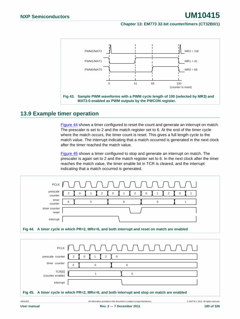
NXP Semiconductors UM10415Chapter 13: EM773 32-bit counter/timers (CT32B0/1)
13.9 Example timer operation
Figure 44 shows a timer configured to reset the count and generate an interrupt on match. The prescaler is set to 2 and the match register set to 6. At the end of the timer cycle where the match occurs, the timer count is reset. This gives a full length cycle to the match value. The interrupt indicating that a match occurred is generated in the next clock after the timer reached the match value.
Figure 45 shows a timer configured to stop and generate an interrupt on match. The prescaler is again set to 2 and the match register set to 6. In the next clock after the timer reaches the match value, the timer enable bit in TCR is cleared, and the interrupt indicating that a match occurred is generated.
Fig 43. Sample PWM waveforms with a PWM cycle length of 100 (selected by MR3) and MAT3:0 enabled as PWM outputs by the PWCON register.
100(counter is reset)
0 41 65
PWM0/MAT0
PWM1/MAT1
PWM2/MAT2 MR2 = 100
MR1 = 41
MR0 = 65
Fig 44. A timer cycle in which PR=2, MRx=6, and both interrupt and reset on match are enabled
PCLK
prescalecounter
interrupt
timercounter
timer counterreset
2222 0 0 0 01 1 1 1
4 5 6 0 1
Fig 45. A timer cycle in which PR=2, MRx=6, and both interrupt and stop on match are enabled
PCLK
prescale counter
interrupt
timer counter
TCR[0](counter enable)
22 0 01
4 5 6
1 0
UM10415 All information provided in this document is subject to legal disclaimers. © NXP B.V. 2011. All rights reserved.
User manual Rev. 2 — 7 December 2011 180 of 326

NXP Semiconductors UM10415Chapter 13: EM773 32-bit counter/timers (CT32B0/1)
13.10 Architecture
The block diagram for 32-bit counter/timer0 and 32-bit counter/timer1 is shown in Figure 46.
Fig 46. 32-bit counter/timer block diagram
reset MAXVAL
TIMER CONTROL REGISTER PRESCALE REGISTER
PRESCALE COUNTERPCLK
enable
CAPTURE REGISTER 0
MATCH REGISTER 3
MATCH REGISTER 2
MATCH REGISTER 1
MATCH REGISTER 0
CAPTURE CONTROL REGISTER
CONTROL
TIMER COUNTERCSN
TCI
CE
=
=
=
=
INTERRUPT REGISTER
EXTERNAL MATCH REGISTER
MATCH CONTROL REGISTER
MAT[3:0]
INTERRUPT
CAP0
STOP ON MATCH
RESET ON MATCH
LOAD[3:0]
UM10415 All information provided in this document is subject to legal disclaimers. © NXP B.V. 2011. All rights reserved.
User manual Rev. 2 — 7 December 2011 181 of 326

14.1 How to read this chapter
The WDT block is identical for all EM773 parts.
14.2 Basic configuration
The WDT is configured using the following registers:
1. Pins: The WDT uses no external pins.
2. Power: In the SYSAHBCLKCTRL register, set bit 15 (Table 17).
3. Peripheral clock: Select the watchdog clock source Table 20) and enable the WDT peripheral clock by writing to the WDTCLKDIV register (Table 22).
Remark: The frequency of the watchdog oscillator is undefined after reset. The watchdog oscillator frequency must be programmed by writing to the WDTOSCCTRL register (see Table 9) before using the watchdog oscillator for the WDT.
4. Lock features: Once the watchdog timer is enabled by setting the WDEN bit in the WDMOD register, the following lock features are in effect:
a. The WDEN bit cannot be changed to 0, that is the WDT cannot be disabled.
b. The watch dog clock source cannot be changed. If the WDT is needed in Deep-sleep mode, select the watch dog oscillator as the clock source before setting the WDEN bit.
14.3 Features
• Internally resets chip if not reloaded during the programmable time-out period.
• Optional windowed operation requires reload to occur between a minimum and maximum time-out period, both programmable.
• Optional warning interrupt can be generated at a programmable time prior to watchdog time-out.
• Programmable 24-bit timer with internal fixed pre-scaler.
• Selectable time period from 1,024 watchdog clocks (TWDCLK 256 4) to over 67 million watchdog clocks (TWDCLK 224 4) in increments of 4 watchdog clocks.
• “Safe” watchdog operation. Once enabled, requires a hardware reset or a Watchdog reset to be disabled.
• A dedicated on-chip watchdog oscillator provides a reliable clock source that cannot be turned off when the Watchdog Timer is running.
• Incorrect feed sequence causes immediate watchdog reset if the watchdog is enabled.
• The watchdog reload value can optionally be protected such that it can only be changed after the “warning interrupt” time is reached.
• Flag to indicate Watchdog reset.
UM10415Chapter 14: EM773 WatchDog Timer (WDT)Rev. 2 — 7 December 2011 User manual
UM10415 All information provided in this document is subject to legal disclaimers. © NXP B.V. 2011. All rights reserved.
User manual Rev. 2 — 7 December 2011 182 of 326

NXP Semiconductors UM10415Chapter 14: EM773 WatchDog Timer (WDT)
14.4 Applications
The purpose of the Watchdog Timer is to reset the microcontroller within a reasonable amount of time if it enters an erroneous state. When enabled, a watchdog event will be generated if the user program fails to feed (or reload) the Watchdog within a predetermined amount of time. The Watchdog event will cause a chip reset if configured to do so.
When a watchdog window is programmed, an early watchdog feed is also treated as a watchdog event. This allows preventing situations where a system failure may still feed the watchdog. For example, application code could be stuck in an interrupt service that contains a watchdog feed. Setting the window such that this would result in an early feed will generate a watchdog event, allowing for system recovery.
.
14.5 General description
The Watchdog consists of a fixed divide-by-4 pre-scaler and a 24-bit counter which decrements when clocked. The minimum value from which the counter decrements is 0xFF. Setting a value lower than 0xFF causes 0xFF to be loaded in the counter. Hence the minimum Watchdog interval is (TWDCLK 256 4) and the maximum Watchdog interval is (TWDCLK 224 4) in multiples of (TWDCLK 4). The Watchdog should be used in the following manner:
• Set the Watchdog timer constant reload value in WDTC register.
• Setup the Watchdog timer operating mode in WDMOD register.
• Set a value for the watchdog window time in WDWINDOW register if windowed operation is required.
• Set a value for the watchdog warning interrupt in the WDWARNINT register if a warning interrupt is required.
• Enable the Watchdog by writing 0xAA followed by 0x55 to the WDFEED register.
• The Watchdog must be fed again before the Watchdog counter reaches zero in order to prevent a watchdog event. If a window value is programmed, the feed must also occur after the watchdog counter passes that value.
When the Watchdog Timer is configured so that a watchdog event will cause a reset and the counter reaches zero, the CPU will be reset, loading the stack pointer and program counter from the vector table as in the case of external reset. The Watchdog time-out flag (WDTOF) can be examined to determine if the Watchdog has caused the reset condition. The WDTOF flag must be cleared by software.
When the Watchdog Timer is configured to generate a warning interrupt, the interrupt will occur when the counter matches the value defined by the WDWARNINT register.
The block diagram of the Watchdog is shown below in the Figure 47. The synchronization logic (PCLK - WDCLK) is not shown in the block diagram.
UM10415 All information provided in this document is subject to legal disclaimers. © NXP B.V. 2011. All rights reserved.
User manual Rev. 2 — 7 December 2011 183 of 326
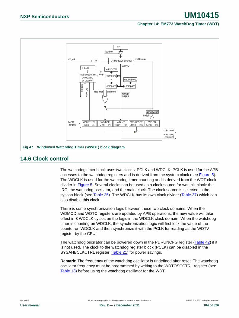
NXP Semiconductors UM10415Chapter 14: EM773 WatchDog Timer (WDT)
14.6 Clock control
The watchdog timer block uses two clocks: PCLK and WDCLK. PCLK is used for the APB accesses to the watchdog registers and is derived from the system clock (see Figure 5). The WDCLK is used for the watchdog timer counting and is derived from the WDT clock divider in Figure 5. Several clocks can be used as a clock source for wdt_clk clock: the IRC, the watchdog oscillator, and the main clock. The clock source is selected in the syscon block (see Table 25). The WDCLK has its own clock divider (Table 27) which can also disable this clock.
There is some synchronization logic between these two clock domains. When the WDMOD and WDTC registers are updated by APB operations, the new value will take effect in 3 WDCLK cycles on the logic in the WDCLK clock domain. When the watchdog timer is counting on WDCLK, the synchronization logic will first lock the value of the counter on WDCLK and then synchronize it with the PCLK for reading as the WDTV register by the CPU.
The watchdog oscillator can be powered down in the PDRUNCFG register (Table 42) if it is not used. The clock to the watchdog register block (PCLK) can be disabled in the SYSAHBCLKCTRL register (Table 21) for power savings.
Remark: The frequency of the watchdog oscillator is undefined after reset. The watchdog oscillator frequency must be programmed by writing to the WDTOSCCTRL register (see Table 13) before using the watchdog oscillator for the WDT.
Fig 47. Windowed Watchdog Timer (WWDT) block diagram
watchdog interrupt
WDRESET (MOD [1])
WDTOF (MOD [2])
WDINT (MOD [3])
WDEN (MOD [0])
chip reset
÷4
feed error
feed ok
wd_clk enable count
MOD register
compare
WDTV
comparein
range
underflow
feed sequence detect and protection
FEED
feed ok
feed ok
compare
0
interrupt compare
24-bit down counter
WDINTVAL
WINDOW
TC
shadow bit
WDPROTECT(MOD [4])
TC write
UM10415 All information provided in this document is subject to legal disclaimers. © NXP B.V. 2011. All rights reserved.
User manual Rev. 2 — 7 December 2011 184 of 326
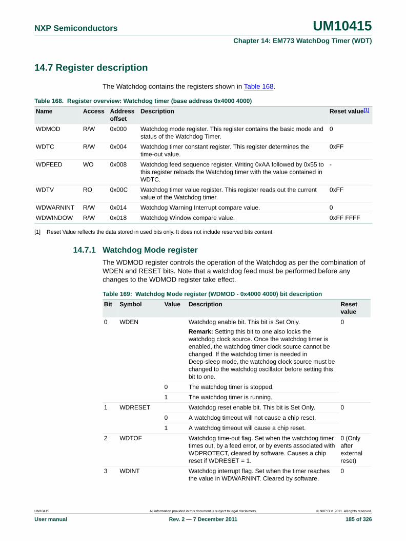
NXP Semiconductors UM10415Chapter 14: EM773 WatchDog Timer (WDT)
14.7 Register description
The Watchdog contains the registers shown in Table 168.
[1] Reset Value reflects the data stored in used bits only. It does not include reserved bits content.
14.7.1 Watchdog Mode register
The WDMOD register controls the operation of the Watchdog as per the combination of WDEN and RESET bits. Note that a watchdog feed must be performed before any changes to the WDMOD register take effect.
Table 168. Register overview: Watchdog timer (base address 0x4000 4000)
Name Access Address offset
Description Reset value[1]
WDMOD R/W 0x000 Watchdog mode register. This register contains the basic mode and status of the Watchdog Timer.
0
WDTC R/W 0x004 Watchdog timer constant register. This register determines the time-out value.
0xFF
WDFEED WO 0x008 Watchdog feed sequence register. Writing 0xAA followed by 0x55 to this register reloads the Watchdog timer with the value contained in WDTC.
-
WDTV RO 0x00C Watchdog timer value register. This register reads out the current value of the Watchdog timer.
0xFF
WDWARNINT R/W 0x014 Watchdog Warning Interrupt compare value. 0
WDWINDOW R/W 0x018 Watchdog Window compare value. 0xFF FFFF
Table 169: Watchdog Mode register (WDMOD - 0x4000 4000) bit description
Bit Symbol Value Description Reset value
0 WDEN Watchdog enable bit. This bit is Set Only.
Remark: Setting this bit to one also locks the watchdog clock source. Once the watchdog timer is enabled, the watchdog timer clock source cannot be changed. If the watchdog timer is needed in Deep-sleep mode, the watchdog clock source must be changed to the watchdog oscillator before setting this bit to one.
0
0 The watchdog timer is stopped.
1 The watchdog timer is running.
1 WDRESET Watchdog reset enable bit. This bit is Set Only. 0
0 A watchdog timeout will not cause a chip reset.
1 A watchdog timeout will cause a chip reset.
2 WDTOF Watchdog time-out flag. Set when the watchdog timer times out, by a feed error, or by events associated with WDPROTECT, cleared by software. Causes a chip reset if WDRESET = 1.
0 (Only after external reset)
3 WDINT Watchdog interrupt flag. Set when the timer reaches the value in WDWARNINT. Cleared by software.
0
UM10415 All information provided in this document is subject to legal disclaimers. © NXP B.V. 2011. All rights reserved.
User manual Rev. 2 — 7 December 2011 185 of 326

NXP Semiconductors UM10415Chapter 14: EM773 WatchDog Timer (WDT)
Once the WDEN, WDPROTECT, or WDRESET bits are set they can not be cleared by software. Both flags are cleared by an external reset or a Watchdog timer reset.
WDTOF The Watchdog time-out flag is set when the Watchdog times out, when a feed error occurs, or when WDPROTECT =1 and an attempt is made to write to the WDTC register. This flag is cleared by software writing a 0 to this bit.
WDINT The Watchdog interrupt flag is set when the Watchdog counter reaches the value specified by WDWARNINT. This flag is cleared when any reset occurs, and is cleared by software by writing a 1 to this bit.
Watchdog reset or interrupt will occur any time the watchdog is running. If a watchdog interrupt occurs in Sleep mode, it will wake up the device.
14.7.2 Watchdog Timer Constant register
The WDTC register determines the time-out value. Every time a feed sequence occurs the WDTC content is reloaded in to the Watchdog timer. This is pre-loaded with the value 0x00 00FF upon reset. Writing values below 0xFF will cause 0x00 00FF to be loaded into the WDTC. Thus the minimum time-out interval is TWDCLK 256 4.
If the WDPROTECT bit in WDMOD = 1, an attempt to change the value of WDTC before the watchdog counter is below the values of WDWARNINT and WDWINDOW will cause a watchdog reset and set the WDTOF flag.
4 WDPROTECT Watchdog update mode. This bit is Set Only. 0
0 The watchdog reload value (WDTC) can be changed at any time.
1 The watchdog reload value (WDTC) can be changed only after the counter is below the value of WDWARNINT and WDWINDOW. Note: this mode is intended for use only when WDRESET =1.
31:5
- Reserved. Read value is undefined, only zero should be written.
-
Table 170. Watchdog operating modes selection
WDEN WDRESET Mode of Operation
0 X (0 or 1) Debug/Operate without the Watchdog running.
1 0 Watchdog interrupt mode: the watchdog warning interrupt will be generated but watchdog reset will not. When this mode is selected, the watchdog counter reaching the value specified by WDWARNINT will set the WDINT flag and the Watchdog interrupt request will be generated.
1 1 Watchdog reset mode: both the watchdog interrupt and watchdog reset are enabled. When this mode is selected, the watchdog counter reaching the value specified by WDWARNINT will set the WDINT flag and the Watchdog interrupt request will be generated, and the watchdog counter reaching zero will reset the microcontroller. A watchdog feed prior to reaching the value of WDWINDOW will also cause a watchdog reset.
Table 169: Watchdog Mode register (WDMOD - 0x4000 4000) bit description
Bit Symbol Value Description Reset value
UM10415 All information provided in this document is subject to legal disclaimers. © NXP B.V. 2011. All rights reserved.
User manual Rev. 2 — 7 December 2011 186 of 326

NXP Semiconductors UM10415Chapter 14: EM773 WatchDog Timer (WDT)
14.7.3 Watchdog Feed register
Writing 0xAA followed by 0x55 to this register will reload the Watchdog timer with the WDTC value. This operation will also start the Watchdog if it is enabled via the WDMOD register. Setting the WDEN bit in the WDMOD register is not sufficient to enable the Watchdog. A valid feed sequence must be completed after setting WDEN before the Watchdog is capable of generating a reset. Until then, the Watchdog will ignore feed errors. After writing 0xAA to WDFEED, access to any Watchdog register other than writing 0x55 to WDFEED causes an immediate reset/interrupt when the Watchdog is enabled, and sets the WDTOF flag. The reset will be generated during the second PCLK following an incorrect access to a Watchdog register during a feed sequence.
14.7.4 Watchdog Timer Value register
The WDTV register is used to read the current value of Watchdog timer counter.
When reading the value of the 24-bit counter, the lock and synchronization procedure takes up to 6 WDCLK cycles plus 6 PCLK cycles, so the value of WDTV is older than the actual value of the timer when it's being read by the CPU.
14.7.5 Watchdog Timer Warning Interrupt register
The WDWARNINT register determines the watchdog timer counter value that will generate a watchdog interrupt. When the watchdog timer counter matches the value defined by WDWARNINT, an interrupt will be generated after the subsequent WDCLK.
A match of the watchdog timer counter to WDWARNINT occurs when the bottom 10 bits of the counter have the same value as the 10 bits of WARNINT, and the remaining upper bits of the counter are all 0. This gives a maximum time of 1,023 watchdog timer counts (4,096 watchdog clocks) for the interrupt to occur prior to a watchdog event. If WARNINT is set to 0, the interrupt will occur at the same time as the watchdog event.
Table 171: Watchdog Timer Constant register (WDTC - 0x4000 4004) bit description
Bit Symbol Description Reset value
23:0 Count Watchdog time-out interval. 0x00 00FF
31:24 - Reserved. Read value is undefined, only zero should be written.
NA
Table 172: Watchdog Feed register (WDFEED - 0x4000 4008) bit description
Bit Symbol Description Reset value
7:0 Feed Feed value should be 0xAA followed by 0x55. -
31:8 - Reserved -
Table 173: Watchdog Timer Value register (WDTV - 0x4000 400C) bit description
Bit Symbol Description Reset value
23:0 Count Counter timer value. 0x00 00FF
31:24 - Reserved. Read value is undefined, only zero should be written.
-
UM10415 All information provided in this document is subject to legal disclaimers. © NXP B.V. 2011. All rights reserved.
User manual Rev. 2 — 7 December 2011 187 of 326
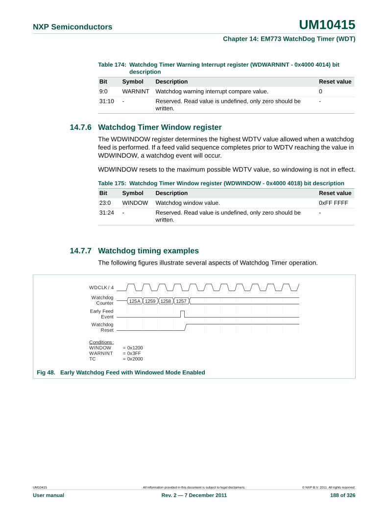
NXP Semiconductors UM10415Chapter 14: EM773 WatchDog Timer (WDT)
14.7.6 Watchdog Timer Window register
The WDWINDOW register determines the highest WDTV value allowed when a watchdog feed is performed. If a feed valid sequence completes prior to WDTV reaching the value in WDWINDOW, a watchdog event will occur.
WDWINDOW resets to the maximum possible WDTV value, so windowing is not in effect.
14.7.7 Watchdog timing examples
The following figures illustrate several aspects of Watchdog Timer operation.
Table 174: Watchdog Timer Warning Interrupt register (WDWARNINT - 0x4000 4014) bit description
Bit Symbol Description Reset value
9:0 WARNINT Watchdog warning interrupt compare value. 0
31:10 - Reserved. Read value is undefined, only zero should be written.
-
Table 175: Watchdog Timer Window register (WDWINDOW - 0x4000 4018) bit description
Bit Symbol Description Reset value
23:0 WINDOW Watchdog window value. 0xFF FFFF
31:24 - Reserved. Read value is undefined, only zero should be written.
-
Fig 48. Early Watchdog Feed with Windowed Mode Enabled
125A 12581259 1257
WDCLK / 4
Watchdog Counter
Early Feed Event
Watchdog Reset
Conditions :WINDOW = 0x1200WARNINT = 0x3FFTC = 0x2000
UM10415 All information provided in this document is subject to legal disclaimers. © NXP B.V. 2011. All rights reserved.
User manual Rev. 2 — 7 December 2011 188 of 326

NXP Semiconductors UM10415Chapter 14: EM773 WatchDog Timer (WDT)
Fig 49. Correct Watchdog Feed with Windowed Mode Enabled
Correct Feed Event
1201 11FF1200
WDCLK / 4
Watchdog Counter
Watchdog Reset
11FC11FD 2000 1FFE1FFF11FE 1FFD 1FFC
Conditions :WDWINDOW = 0x1200WDWARNINT = 0x3FFWDTC = 0x2000
Fig 50. Watchdog Warning Interrupt
Watchdog Interrupt
0403 04010402
WDCLK / 4
Watchdog Counter 03FE03FF 03FD 03FB03FC0400 03FA 03F9
Conditions :WINDOW = 0x1200WARNINT = 0x3FFTC = 0x2000
UM10415 All information provided in this document is subject to legal disclaimers. © NXP B.V. 2011. All rights reserved.
User manual Rev. 2 — 7 December 2011 189 of 326

15.1 Features
• Includes ROM-based application services
• Power Management services
• Clocking services
15.2 Description
The API calls to the ROM are performed by executing functions which are pointed by a pointer within the ROM Driver Table. Figure 51 shows the pointer structure used to call the Power Profiles API.
15.3 Definitions
The following elements have to be defined in an application that uses the power profiles:
typedef struct _PWRD {void (*set_pll)(unsigned int cmd[], unsigned int resp[]);void (*set_power)(unsigned int cmd[], unsigned int resp[]);
} PWRD;
UM10415Chapter 15: EM773 Power profilesRev. 2 — 7 December 2011 User manual
Fig 51. Power profiles pointer structure
Ptr to ROM Driver table
Ptr to Device Table 2
Ptr to Device Table 1
Ptr to Device Table 0
…
Ptr to Device Table n
set_pll
set_power
Ptr to Function 2
Ptr to Function 0
Ptr to Function 1
…
Ptr to Function n
Power API function table
Device n
ROM Driver Table
0x1FFF 2004
0x1FFF 1FF8
0x1FFF 1FFC
0x1FFF 2000
0x1FFF 2004
Ptr to PowerAPI Table
UM10415 All information provided in this document is subject to legal disclaimers. © NXP B.V. 2011. All rights reserved.
User manual Rev. 2 — 7 December 2011 190 of 326

NXP Semiconductors UM10415Chapter 15: EM773 Power profiles
typedef struct _ROM {const PWRD * pWRD;
} ROM;ROM ** rom = (ROM **) (0x1FFF1FF8 + 3 * sizeof(ROM**));unsigned int command[4], result[2];
15.4 Clocking routine
15.4.1 set_pll
This routine sets up the system PLL according to the calling arguments. If the expected clock can be obtained by simply dividing the system PLL input, set_pll bypasses the PLL to lower system power consumption.
Remark: Before this routine is invoked, the PLL clock source (IRC/system oscillator) must be selected (Table 12), the main clock source must be set to the input clock to the system PLL (Table 14) and the system/AHB clock divider must be set to 1 (Table 16).
set_pll attempts to find a PLL setup that matches the calling parameters. Once a combination of a feedback divider value (SYSPLLCTRL, M), a post divider ratio (SYSPLLCTRL, P) and the system/AHB clock divider (SYSAHBCLKDIV) is found, set_pll applies the selected values and switches the main clock source selection to the system PLL clock out (if necessary).
The routine returns a result code that indicates if the system PLL was successfully set (PLL_CMD_SUCCESS) or not (in which case the result code identifies what went wrong). The current system frequency value is also returned. The application should use this information to adjust other clocks in the device (the SSP, UART, and WDT clocks, and/or clockout).
The following definitions are needed when making set_pll power routine calls:
/* set_pll mode options */#define CPU_FREQ_EQU 0#define CPU_FREQ_LTE 1#define CPU_FREQ_GTE 2#define CPU_FREQ_APPROX 3/* set_pll result0 options */#define PLL_CMD_SUCCESS 0#define PLL_INVALID_FREQ 1#define PLL_INVALID_MODE 2
Table 176. set_pll routine
Routine set_pll
Input Param0: system PLL input frequency (in kHz)
Param1: expected system clock (in kHz)
Param2: mode (CPU_FREQ_EQU, CPU_FREQ_LTE, CPU_FREQ_GTE, CPU_FREQ_APPROX)
Param3: system PLL lock time-out
Result Result0: PLL_CMD_SUCCESS | PLL_INVALID_FREQ | PLL_INVALID_MODE | PLL_FREQ_NOT_FOUND | PLL_NOT_LOCKED
Result1: system clock (in kHz)
UM10415 All information provided in this document is subject to legal disclaimers. © NXP B.V. 2011. All rights reserved.
User manual Rev. 2 — 7 December 2011 191 of 326

NXP Semiconductors UM10415Chapter 15: EM773 Power profiles
#define PLL_FREQ_NOT_FOUND 3#define PLL_NOT_LOCKED 4
For a simplified clock configuration scheme see Figure 53. For more details see Figure 3.
15.4.1.1 Param0: system PLL input frequency and Param1: expected system clock
set_pll looks for a setup in which the system PLL clock does not exceed 50 MHz. It easily finds a solution when the ratio between the expected system clock and the system PLL input frequency is an integer value, but it can also find solutions in other cases.
The system PLL input frequency (Param0) must be between 10000 to 25000 kHz (10 MHz to 25 MHz) inclusive. The expected system clock (Param1) must be between 1 and 50000 kHz inclusive. If either of these requirements is not met, set_pll returns PLL_INVALID_FREQ and returns Param0 as Result1 since the PLL setting is unchanged.
15.4.1.2 Param2: mode
The first priority of set_pll is to find a setup that generates the system clock at exactly the rate specified in Param1. If it is unlikely that an exact match can be found, input parameter mode (Param2) should be used to specify if the actual system clock can be less than or equal, greater than or equal or approximately the value specified as the expected system clock (Param1).
A call specifying CPU_FREQ_EQU will only succeed if the PLL can output exactly the frequency requested in Param1.
CPU_FREQ_LTE can be used if the requested frequency should not be exceeded (such as overall current consumption and/or power budget reasons).
CPU_FREQ_GTE helps applications that need a minimum level of CPU processing capabilities.
CPU_FREQ_APPROX results in a system clock that is as close as possible to the requested value (it may be greater than or less than the requested value).
If an illegal mode is specified, set_pll returns PLL_INVALID_MODE. If the expected system clock is out of the range supported by this routine, set_pll returns PLL_FREQ_NOT_FOUND. In these cases the current PLL setting is not changed and Param0 is returned as Result1.
15.4.1.3 Param3: system PLL lock time-out
It should take no more than 100 s for the system PLL to lock if a valid configuration is selected. If Param3 is zero, set_pll will wait indefinitely for the PLL to lock. A non-zero value indicates how many times the code will check for a successful PLL lock event before it returns PLL_NOT_LOCKED. In this case the PLL settings are unchanged and Param0 is returned as Result1.
Remark: The time it takes the PLL to lock depends on the selected PLL input clock source (IRC/system oscillator) and its characteristics. The selected source can experience more or less jitter depending on the operating conditions such as power supply and/or ambient temperature. This is why it is suggested that when a good known clock source is used and a PLL_NOT_LOCKED response is received, the set_pll routine should be invoked several times before declaring the selected PLL clock source invalid.
UM10415 All information provided in this document is subject to legal disclaimers. © NXP B.V. 2011. All rights reserved.
User manual Rev. 2 — 7 December 2011 192 of 326

NXP Semiconductors UM10415Chapter 15: EM773 Power profiles
Hint: setting Param3 equal to the system PLL frequency [Hz] divided by 10000 will provide more than enough PLL lock-polling cycles.
15.4.1.4 Code examples
The following examples illustrate some of the features of set_pll discussed above.
15.4.1.4.1 Invalid frequency (device maximum clock rate exceeded)
command[0] = 12000;command[1] = 60000;command[2] = CPU_FREQ_EQU;command[3] = 0;(*rom)->pWRD->set_pll(command, result);
The above code specifies a 12 MHz PLL input clock and a system clock of exactly 60 MHz. The application was ready to infinitely wait for the PLL to lock. But the expected system clock of 60 MHz exceeds the maximum of 50 MHz. Therefore set_pll returns PLL_INVALID_FREQ in result[0] and 12000 in result[1] without changing the PLL settings.
15.4.1.4.2 Invalid frequency selection (system clock divider restrictions)
command[0] = 12000;command[1] = 40;command[2] = CPU_FREQ_LTE;command[3] = 0;(*rom)->pWRD->set_pll(command, result);
The above code specifies a 12 MHz PLL input clock, a system clock of no more than 40 kHz and no time-out while waiting for the PLL to lock. Since the maximum divider value for the system clock is 255 and running at 40 kHz would need a divide by value of 300, set_pll returns PLL_INVALID_FREQ in result[0] and 12000 in result[1] without changing the PLL settings.
15.4.1.4.3 Exact solution cannot be found (PLL)
command[0] = 12000;command[1] = 25000;command[2] = CPU_FREQ_EQU;command[3] = 0;(*rom)->pWRD->set_pll(command, result);
The above code specifies a 12 MHz PLL input clock and a system clock of exactly 25 MHz. The application was ready to infinitely wait for the PLL to lock. Since there is no valid PLL setup within earlier mentioned restrictions, set_pll returns PLL_FREQ_NOT_FOUND in result[0] and 12000 in result[1] without changing the PLL settings.
15.4.1.4.4 System clock less than or equal to the expected value
command[0] = 12000;command[1] = 25000;command[2] = CPU_FREQ_LTE;command[3] = 0;
UM10415 All information provided in this document is subject to legal disclaimers. © NXP B.V. 2011. All rights reserved.
User manual Rev. 2 — 7 December 2011 193 of 326

NXP Semiconductors UM10415Chapter 15: EM773 Power profiles
(*rom)->pWRD->set_pll(command, result);
The above code specifies a 12 MHz PLL input clock, a system clock of no more than 25 MHz and no locking time-out. set_pll returns PLL_CMD_SUCCESS in result[0] and 24000 in result[1]. The new system clock is 24 MHz.
15.4.1.4.5 System clock greater than or equal to the expected value
command[0] = 12000;command[1] = 25000;command[2] = CPU_FREQ_GTE;command[3] = 0;(*rom)->pWRD->set_pll(command, result);
The above code specifies a 12 MHz PLL input clock, a system clock of at least 25 MHz and no locking time-out. set_pll returns PLL_CMD_SUCCESS in result[0] and 36000 in result[1]. The new system clock is 36 MHz.
15.4.1.4.6 System clock approximately equal to the expected value
command[0] = 12000;command[1] = 16500;command[2] = CPU_FREQ_APPROX;command[3] = 0;(*rom)->pWRD->set_pll(command, result);
The above code specifies a 12 MHz PLL input clock, a system clock of approximately 16.5 MHz and no locking time-out. set_pll returns PLL_CMD_SUCCESS in result[0] and 16000 in result[1]. The new system clock is 16 MHz.
15.5 Power routine
15.5.1 set_power
This routine configures the device’s internal power control settings according to the calling arguments. The goal is to reduce active power consumption while maintaining the feature of interest to the application close to its optimum.
Remark: The set_power routine was designed for systems employing the configuration of SYSAHBCLKDIV = 1 (System clock divider register, see Table 16 and Figure 53). Using this routine in an application with the system clock divider not equal to 1 might not improve microcontroller’s performance as much as in setups when the main clock and the system clock are running at the same rate.
set_power returns a result code that reports whether the power setting was successfully changed or not.
UM10415 All information provided in this document is subject to legal disclaimers. © NXP B.V. 2011. All rights reserved.
User manual Rev. 2 — 7 December 2011 194 of 326

NXP Semiconductors UM10415Chapter 15: EM773 Power profiles
Fig 52. Power profiles usage
using power profiles and changing system clock
current_clock,new_clock , new_mode
use power routine callto change mode to
DEFAULT
use either clocking routine call or custom code to change system clock
from current_clock to new_clock
use power routine callto change mode to
new_mode
end
Fig 53. EM773 clock configuration for power API use
SYS PLL
irc_osc_clk
sys_osc_clk
irc_osc_clk
wdt_osc_clk
MAINCLKSEL
SYSPLLCLKSEL
CLOCKDIVIDER
SYSAHBCLKCTRL[1](ROM enable)
SYSAHBCLKCTRL[18](SPI1 enable)
CLOCKDIVIDER Peripherals
main clock system clock
sys_pllclkin
sys_pllclkout7
ARMCORTEX-M0
ROM
SPI1
SYSAHBCLKDIV
UM10415 All information provided in this document is subject to legal disclaimers. © NXP B.V. 2011. All rights reserved.
User manual Rev. 2 — 7 December 2011 195 of 326

NXP Semiconductors UM10415Chapter 15: EM773 Power profiles
The following definitions are needed for set_power routine calls:
/* set_power mode options */#define PWR_DEFAULT 0#define PWR_CPU_PERFORMANCE 1#define PWR_EFFICIENCY 2#define PWR_LOW_CURRENT 3/* set_power result0 options */#define PWR_CMD_SUCCESS 0#define PWR_INVALID_FREQ 1#define PWR_INVALID_MODE 2
For a simplified clock configuration scheme see Figure 53. For more details see Figure 3.
15.5.1.1 Param0: main clock
The main clock is the clock rate the microcontroller uses to source the system’s and the peripherals’ clock. It is configured by either a successful execution of the clocking routine call or a similar code provided by the user. This operand must be an integer between 1 to 50 MHz inclusive. If a value out of this range is supplied, set_power returns PWR_INVALID_FREQ and does not change the power control system.
15.5.1.2 Param1: mode
The input parameter mode (Param1) specifies one of four available power settings. If an illegal selection is provided, set_power returns PWR_INVALID_MODE and does not change the power control system.
PWR_DEFAULT keeps the device in a baseline power setting similar to its reset state.
PWR_CPU_PERFORMANCE configures the microcontroller so that it can provide more processing capability to the application. CPU performance is 30% better than the default option.
PWR_EFFICIENCY setting was designed to find a balance between active current and the CPU’s ability to execute code and process data. In this mode the device outperforms the default mode both in terms of providing higher CPU performance and lowering active current.
PWR_LOW_CURRENT is intended for those solutions that focus on lowering power consumption rather than CPU performance.
15.5.1.3 Param2: system clock
The system clock is the clock rate at which the microcontroller core is running when set_power is called. This parameter is an integer between from 1 and 50 MHz inclusive.
Table 177. set_power routine
Routine set_power
Input Param0: main clock (in MHz)
Param1: mode (PWR_DEFAULT, PWR_CPU_PERFORMANCE, PWR_ EFFICIENCY, PWR_LOW_CURRENT)
Param2: system clock (in MHz)
Result Result0: PWR_CMD_SUCCESS | PWR_INVALID_FREQ | PWR_INVALID_MODE
UM10415 All information provided in this document is subject to legal disclaimers. © NXP B.V. 2011. All rights reserved.
User manual Rev. 2 — 7 December 2011 196 of 326

NXP Semiconductors UM10415Chapter 15: EM773 Power profiles
15.5.1.4 Code examples
The following examples illustrate some of the set_power features discussed above.
15.5.1.4.1 Invalid frequency (device maximum clock rate exceeded)
command[0] = 60;command[1] = PWR_CPU_PERFORMANCE;command[2] = 60;(*rom)->pWRD->set_power(command, result);
The above setup would be used in a system running at the main and system clock of 60 MHz, with a need for maximum CPU processing power. Since the specified 60 MHz clock is above the 50 MHz maximum, set_power returns PWR_INVALID_FREQ in result[0] without changing anything in the existing power setup.
15.5.1.4.2 An applicable power setup
command[0] = 24;command[1] = PWR_CPU_EFFICIENCY;command[2] = 24;(*rom)->pWRD->set_power(command, result);
The above code specifies that an application is running at the main and system clock of 24 MHz with emphasis on efficiency. set_power returns PWR_CMD_SUCCESS in result[0] after configuring the microcontroller’s internal power control features.
UM10415 All information provided in this document is subject to legal disclaimers. © NXP B.V. 2011. All rights reserved.
User manual Rev. 2 — 7 December 2011 197 of 326

16.1 How to read this chapter
The system tick timer (SysTick timer) is part of the ARM Cortex-M0 core and is identical for all EM773 parts.
16.2 Basic configuration
The system tick timer is configured using the following registers:
1. Pins: The system tick timer uses no external pins.
2. Power: The system tick timer is enabled through the SysTick control register (Section 21.5.4.1). The system tick timer clock is fixed to half the frequency of the system clock.
16.3 Features
• Simple 24-bit timer.
• Uses dedicated exception vector.
• Clocked internally by the system clock or the system clock/2.
16.4 General description
The block diagram of the SysTick timer is shown below in the Figure 54.
The SysTick timer is an integral part of the Cortex-M0. The SysTick timer is intended to generate a fixed 10 millisecond interrupt for use by an operating system or other system management software.
UM10415Chapter 16: EM773 System tick timer Rev. 2 — 7 December 2011 User manual
Fig 54. System tick timer block diagram
system clock
reference clock= system clock/2
SYST_CALIB
SYST_RVR
SYST_CVR24-bit down counter
ENABLE
SYST_CSR
private peripheral
bus
System Tick interrupt
TICKINTCOUNTFLAG
loadunder-
flowcount
enable
clock
load data
1
0
SYST_CSRbit CLKSOURCE
UM10415 All information provided in this document is subject to legal disclaimers. © NXP B.V. 2011. All rights reserved.
User manual Rev. 2 — 7 December 2011 198 of 326

NXP Semiconductors UM10415Chapter 16: EM773 System tick timer
Since the SysTick timer is a part of the Cortex-M0, it facilitates porting of software by providing a standard timer that is available on Cortex-M0 based devices. The SysTick timer can be used for:
• An RTOS tick timer which fires at a programmable rate (for example 100 Hz) and invokes a SysTick routine.
• A high-speed alarm timer using the core clock.
• A simple counter. Software can use this to measure time to completion and time used.
• An internal clock source control based on missing/meeting durations. The COUNTFLAG bit-field in the control and status register can be used to determine if an action completed within a set duration, as part of a dynamic clock management control loop.
Refer to the Cortex-M0 User Guide for details.
16.5 Register description
The systick timer registers are located on the ARM Cortex-M0 private peripheral bus (see Figure 62), and are part of the ARM Cortex-M0 core peripherals. For details, see Section 21.5.4.
[1] Reset Value reflects the data stored in used bits only. It does not include content of reserved bits.
16.5.1 System Timer Control and status register
The SYST_CSR register contains control information for the SysTick timer and provides a status flag. This register is part of the ARM Cortex-M0 core system timer register block. For a bit description of this register, see Section 21.5.4 “System timer, SysTick”.
This register determines the clock source for the system tick timer.
Table 178. Register overview: SysTick timer (base address 0xE000 E000)
Name Access Address offset
Description Reset value[1]
SYST_CSR R/W 0x010 System Timer Control and status register 0x000 0000
SYST_RVR R/W 0x014 System Timer Reload value register 0
SYST_CVR R/W 0x018 System Timer Current value register 0
SYST_CALIB R/W 0x01C System Timer Calibration value register 0x4
UM10415 All information provided in this document is subject to legal disclaimers. © NXP B.V. 2011. All rights reserved.
User manual Rev. 2 — 7 December 2011 199 of 326
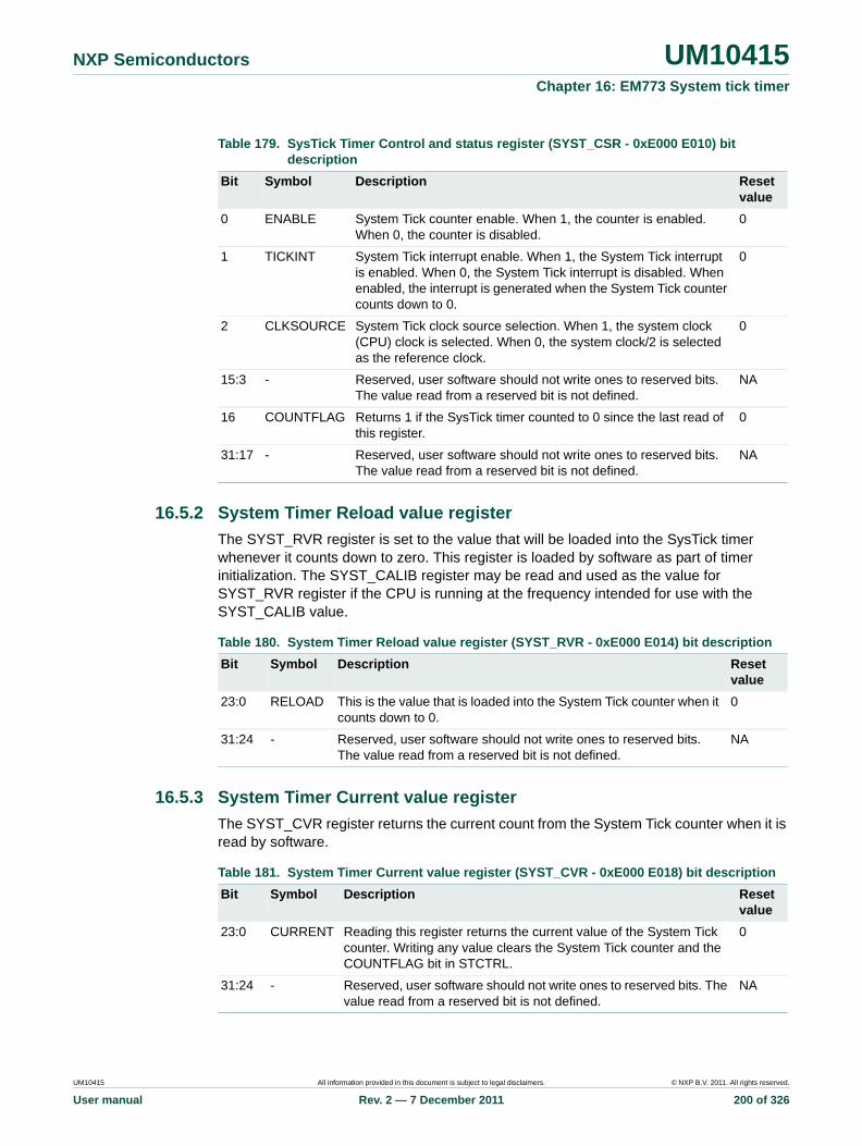
NXP Semiconductors UM10415Chapter 16: EM773 System tick timer
16.5.2 System Timer Reload value register
The SYST_RVR register is set to the value that will be loaded into the SysTick timer whenever it counts down to zero. This register is loaded by software as part of timer initialization. The SYST_CALIB register may be read and used as the value for SYST_RVR register if the CPU is running at the frequency intended for use with the SYST_CALIB value.
16.5.3 System Timer Current value register
The SYST_CVR register returns the current count from the System Tick counter when it is read by software.
Table 179. SysTick Timer Control and status register (SYST_CSR - 0xE000 E010) bit description
Bit Symbol Description Reset value
0 ENABLE System Tick counter enable. When 1, the counter is enabled. When 0, the counter is disabled.
0
1 TICKINT System Tick interrupt enable. When 1, the System Tick interrupt is enabled. When 0, the System Tick interrupt is disabled. When enabled, the interrupt is generated when the System Tick counter counts down to 0.
0
2 CLKSOURCE System Tick clock source selection. When 1, the system clock (CPU) clock is selected. When 0, the system clock/2 is selected as the reference clock.
0
15:3 - Reserved, user software should not write ones to reserved bits. The value read from a reserved bit is not defined.
NA
16 COUNTFLAG Returns 1 if the SysTick timer counted to 0 since the last read of this register.
0
31:17 - Reserved, user software should not write ones to reserved bits. The value read from a reserved bit is not defined.
NA
Table 180. System Timer Reload value register (SYST_RVR - 0xE000 E014) bit description
Bit Symbol Description Reset value
23:0 RELOAD This is the value that is loaded into the System Tick counter when it counts down to 0.
0
31:24 - Reserved, user software should not write ones to reserved bits. The value read from a reserved bit is not defined.
NA
Table 181. System Timer Current value register (SYST_CVR - 0xE000 E018) bit description
Bit Symbol Description Reset value
23:0 CURRENT Reading this register returns the current value of the System Tick counter. Writing any value clears the System Tick counter and the COUNTFLAG bit in STCTRL.
0
31:24 - Reserved, user software should not write ones to reserved bits. The value read from a reserved bit is not defined.
NA
UM10415 All information provided in this document is subject to legal disclaimers. © NXP B.V. 2011. All rights reserved.
User manual Rev. 2 — 7 December 2011 200 of 326
NXP Semiconductors UM10415Chapter 16: EM773 System tick timer
16.5.4 System Timer Calibration value register (SYST_CALIB - 0xE000 E01C)
The value of the SYST_CALIB register is driven by the value of the SYSTCKCAL register in the system configuration block (see Table 29).
16.6 Functional description
The SysTick timer is a 24-bit timer that counts down to zero and generates an interrupt. The intent is to provide a fixed 10 millisecond time interval between interrupts. The SysTick timer is clocked from the CPU clock (the system clock, see Figure 3) or from the reference clock, which is fixed to half the frequency of the CPU clock. In order to generate recurring interrupts at a specific interval, the SYST_RVR register must be initialized with the correct value for the desired interval. A default value is provided in the SYST_CALIB register and may be changed by software. The default value gives a 10 millisecond interrupt rate if the CPU clock is set to 50 MHz.
16.7 Example timer calculations
To use the system tick timer, do the following:
1. Program the SYST_RVR register with the reload value RELOAD to obtain the desired time interval.
2. Clear the SYST_CVR register by writing to it. This ensures that the timer will count from the SYST_RVR value rather than an arbitrary value when the timer is enabled.
3. Program the SYST_SCR register with the value 0x7 which enables the SysTick timer and the SysTick timer interrupt.
The following example illustrates selecting the SysTick timer reload value to obtain a 10 ms time interval with the EM773 system clock set to 50 MHz.
Example (system clock = 50 MHz)
The system tick clock = system clock = 50 MHz. Bit CLKSOURCE in the SYST_CSR register set to 1 (system clock).
RELOAD = (system tick clock frequency 10 ms) 1 = (50 MHz 10 ms) 1 = 5000001 = 499999 = 0x0007A11F.
Table 182. System Timer Calibration value register (SYST_CALIB - 0xE000 E01C) bit description
Bit Symbol Value Description Reset value
23:0 TENMS See Table 264. 0x4
29:24 - Reserved, user software should not write ones to reserved bits. The value read from a reserved bit is not defined.
NA
30 SKEW See Table 264. 0
31 NOREF See Table 264. 0
UM10415 All information provided in this document is subject to legal disclaimers. © NXP B.V. 2011. All rights reserved.
User manual Rev. 2 — 7 December 2011 201 of 326

17.1 How to read this chapter
The EM773 Metrology Engine is available on part EM773 only.
17.2 Introduction
The Metrology Engine performs electricity measurements for one second periods. The bandwidth for the voltage and current inputs is 2 kHz. This means that for 50 Hz mains, up to 40 harmonics can be measured, and for 60 Hz mains up to 33 harmonics.
Figure 55 shows the EM773 with an example of the external measurement circuitry connected to the Metrology Engine. In this case the current measurements are done using a resistor Rshunt and two current measurement channels I_HIGHGAIN and I_LOWGAIN. Voltage is measured using a resistor voltage divider and the VOLTAGE channel.
The opamps in the measurement circuit amplify or attenuate the mains current and voltage signals to the level required by the Metrology Engine. The opamps also apply a DC-bias in order to enable the measurement of AC signals. Finally, the opamps can also be used as low-pass filters to limit the input signal bandwidth to 2 kHz.
UM10415Chapter 17: EM773 Metrology engineRev. 2 — 7 December 2011 User manual
Fig 55. EM773 with external measurement circuitry connected to Metrology Engine
Mains in
Load
Opamp
Metrology
EM773
Rshunt
RR
VDD
Power
engine
I2C/SPI/UART Power meterData outputVSS
VOLTAGE
I_HIGHGAIN
I_LOWGAIN
Supply
UM10415 All information provided in this document is subject to legal disclaimers. © NXP B.V. 2011. All rights reserved.
User manual Rev. 2 — 7 December 2011 202 of 326

NXP Semiconductors UM10415Chapter 17: EM773 Metrology engine
17.3 Features
• Metrology Engine for Energy Measurements
• Outputs RMS voltage (V), RMS current (I), active power (P), apparent power (S), non-active power (N), power factor (PF), fundamental reactive power (Q1), fundamental apparent power (S1), fundamental power factor (PF1), non-fundamental apparent power (SN) and current total harmonic distortion (THDI) according to IEEE Std 1459-2010
• Minimum configuration: One voltage input and one current input
• Optional second current input for increased dynamic range
• Measurement range from VSS to VDD. Do not exceed the VDD voltage level
• Input signal bandwidth 2 kHz
17.4 Pin description
Table 183 gives a brief summary of the Metrology related pins.
17.4.1 I_HIGHGAIN
The I_HIGHGAIN input pin is the default input for current measurements.
The analog front end external to the EM773 must maintain the voltage at the I_HIGHGAIN pin between VSS and VDD. This requires that a DC bias is added when measuring AC signals. For maximum dynamic range this bias should be 0.5 * VDD.
17.4.2 I_LOWGAIN
The I_LOWGAIN input pin is used for optional low-gain current measurements. Using this input increases the dynamic range for the current measurements compared to high-gain only operation.
Table 183. Serial Wire Debug pin description
Pin Name Type Description
I_HIGHGAIN Input Analog Input. The Metrology Engine measures the highgain current on this input. An external circuit must convert the AC measurement current to the input voltage range.
Remark: The maximum input voltage must not exceed VDD.
I_LOWGAIN Input Analog Input. The Metrology Engine measures the lowgain current on this input. An external circuit must convert the AC measurement current to the input voltage range.
Remark: The maximum input voltage must not exceed VDD.
VOLTAGE Input Analog Input. The Metrology Engine measures the voltage on this input. An external circuit must convert the AC measurement voltage to this voltage range.
Remark: The maximum input voltage must not exceed VDD.
VDD Input Reference voltage for the Metrology Engine.
UM10415 All information provided in this document is subject to legal disclaimers. © NXP B.V. 2011. All rights reserved.
User manual Rev. 2 — 7 December 2011 203 of 326
NXP Semiconductors UM10415Chapter 17: EM773 Metrology engine
The analog front end external to the EM773 must maintain the voltage at the I_LOWGAIN pin between VSS and VDD. This requires that a DC bias is added when measuring AC signals. For maximum dynamic range this bias should be 0.5 * VDD. For recommended operation, the gain of the analog front end for the I_LOWGAIN channel external to the EM773 should approximately be 1/16 times the gain for the I_HIGHGAIN channel.
17.4.3 VOLTAGE
The VOLTAGE input pin is the input for voltage measurements.
The analog front end external to the EM773 must maintain the voltage at the VOLTAGE pin between VSS and VDD. This requires that a DC bias is added when measuring AC signals. For maximum dynamic range this bias should be 0.5 * VDD.
17.5 Output definitions
The outputs of the Metrology Engine are described in this Chapter. The definitions used in this section are according to IEEE Std 1459-2010.
17.5.1 Output for sinusoidal and non-sinusoidal voltage and sinusoidal and non-sinusoidal current
The below parameters are directly measured by the Metrology Engine. Other, derived parameters such as kWh Energy registers can be calculated by the application on the microcontroller core using this data.
Voltage: V — The root-mean-square voltage V in Volt (V) is measured according to:
(5)
In this formula, k is the index of the internal voltage samples v inside the Metrology Engine and T is the sample period of the Metrology Engine. The product kT = 1 second.
Current: I — The root-mean-square current in Ampere (A) is measured according to:
(6)
In this formula i are the current samples inside the Metrology Engine.
kT
dtvkT
V
21
kT
dtikT
I
21
UM10415 All information provided in this document is subject to legal disclaimers. © NXP B.V. 2011. All rights reserved.
User manual Rev. 2 — 7 December 2011 204 of 326

NXP Semiconductors UM10415Chapter 17: EM773 Metrology engine
Apparent Power: S — The apparent power S in Volt-Ampere (VA) is measured as the product of the RMS voltage and RMS current:
(7)
Active Power: P — The active power P in Watt (W) is measured according to:
(8)
Non-active Power: N — The non-active power N in Volt-Ampere-reactive (var) is measured according to:
(9)
Power Factor: PF — The dimensionless parameter power factor PF is measured as the ratio between active power and apparent power.
(10)
17.5.2 Additional output for sinusoidal voltage and sinusoidal and non-sinusoidal current
The Metrology Engine output described in this chapter provides additional information for sinusoidal voltages and sinusoidal or non-sinusoidal currents.
According to IEEE Std 1459-2010 these calculations are valid if the voltage waveform has significantly lower distortion than the current waveform. In this case the fundamental active power P1 approximately equals the active power P described above.
Fundamental Reactive Power: Q1 — The fundamental reactive power in Volt-Ampere-reactive (var) is measured according to:
(11)
In this formula, k is the index of the fundamental voltage samples v1 and fundamental current samples i1 inside the Metrology Engine and T is the sample period of the Metrology Engine.
VIS
kT
vidtkT
P
1
22 PSN
S
PPF
kT
dtdtvikT
Q
111
UM10415 All information provided in this document is subject to legal disclaimers. © NXP B.V. 2011. All rights reserved.
User manual Rev. 2 — 7 December 2011 205 of 326

NXP Semiconductors UM10415Chapter 17: EM773 Metrology engine
Fundamental Apparent Power: S1 — The fundamental apparent power S1 in Volt-Ampere (VA) is measured according to:
(12)
Fundamental Power Factor: PF1 — The dimensionless parameter fundamental power factor PF1 is measured as the ratio between fundamental active power P1 and fundamental apparent power S1:
(13)
Nonfundamental Apparent Power: SN — The nonfundamental apparent power SN in Volt-Ampere (VA) is measured according to:
(14)
Current Total Harmonic Distortion: THDI — This dimensionless parameter is measured using the approximation formula below, which is accurate within 1% for voltages with THDV < 0.05 and for currents with THDI > 0.4. For values outside this range it's an indicative approximation.
(15)
21
211 QPS
1
11 S
PPF
21
2 SSSN
1S
STHD N
I
UM10415 All information provided in this document is subject to legal disclaimers. © NXP B.V. 2011. All rights reserved.
User manual Rev. 2 — 7 December 2011 206 of 326

NXP Semiconductors UM10415Chapter 17: EM773 Metrology engine
17.6 Operation
This section explains the configuration data and calibration procedure for the Metrology Engine. Details on the Metrology Engine interface are described in Chapter 18.
17.6.1 Configuration data
Summarizes the Metrology Engine configuration parameters.
17.6.1.1 Voltage measurement input range Vpp
The parameter Vpp depends on transfer of the analog input circuit in front of the Metrology Engine and it sets the peak-to-peak range for the voltage channel (in Volt).
Examples: For 110 V mains this value will be at least 22 * 110 = 311 V and for 230 V mains at least 650 V. In practice these values need to be larger, because margins for mains voltage fluctuations and for component tolerances need to be accounted for in the input circuit design.
The transfer of the analog input circuit in front of the Metrology Engine must guarantee that the signal at the VOLTAGE input of the Energy Measurement IC is between VSS and VDD.
17.6.1.2 Current measurement input range I1pp
The parameter I1pp for the I_HIGHGAIN input depends on transfer of the analog input circuit in front of the Metrology Engine and it sets the peak-to-peak range for the first current channel (in Ampere).
Example: For a single current-channel 16 A meter this value will be at least 22 * 16 = 45.3 A. For a two current-channel 16 A meter this range will cover the range from 0 to 1 A and the corresponding value for I1pp will be at least 22 * 1 = 2.83 A. In practice the above values need to be larger, because margins for component tolerances need to be accounted for in the input circuit design.
The transfer of the analog input circuit in front of the Metrology Engine must guarantee that the signal at the I_HIGHGAIN input of the Energy Measurement IC is between VSS and VDD.
Table 184. Metrology Engine configuration parameters
Member Description
Vpp Voltage measurement input range (in Volt peak-peak) for VOLTAGE channel
I1pp Current measurement input range (in Ampere peak-peak) for I_HIGHGAIN channel
I2pp Current measurement input range (in Ampere peak-peak) for I_LOWGAIN channel
DeltaPhi1 Phase error correction angle (in radian) for I_HIGHGAIN channel
DeltaPhi2 Phase error correction angle (in radian) for I_LOWGAIN channel
UM10415 All information provided in this document is subject to legal disclaimers. © NXP B.V. 2011. All rights reserved.
User manual Rev. 2 — 7 December 2011 207 of 326
NXP Semiconductors UM10415Chapter 17: EM773 Metrology engine
17.6.1.3 Current measurement input range I2pp
The parameter I2pp for the I_LOWGAIN input depends on the transfer of the analog input circuit in front of the Metrology Engine and it sets the peak-to-peak range for the second current channel (in Ampere). The input circuit for this channel should be designed in such a way that this range is approximately 16 * I1pp for an optimized accuracy curve.
Example: For a two current-channel 16 A meter this range will cover the range from 1A to 16 A and the corresponding value for I1pp will be at least 22 * 16 = 45.3 A In practice this value needs to be larger, because margins for component tolerances need to be accounted for in the input circuit design.
The transfer of the analog input circuit in front of the Metrology Engine must guarantee that the signal at the I_LOWGAIN input of the Energy Measurement IC is between VSS and VDD.
Remark: If there is no second current measurement channel present, this value must be set to zero.
17.6.1.4 Phase error correction angle DeltaPhi1
Due to component differences, a phase error can occur between the VOLTAGE and I_HIGHGAIN channels. This error needs to be corrected for accurate measurements.
The parameter DeltaPhi1 contains the correction angle (in radian) to compensate a phase error between the VOLTAGE channel and the I_HIGHGAIN current channel.
17.6.1.5 Phase error correction angle DeltaPhi2
Due to component differences, a phase error can occur between the VOLTAGE and I_LOWGAIN channels (if this channel is used). This error needs to be corrected for accurate measurements.
The parameter DeltaPhi2 contains the correction angle (in radian) to compensate a phase error between the VOLTAGE channel and the I_LOWGAIN current channel.
If there is no second current measurement channel present, this value can be set to zero.
UM10415 All information provided in this document is subject to legal disclaimers. © NXP B.V. 2011. All rights reserved.
User manual Rev. 2 — 7 December 2011 208 of 326
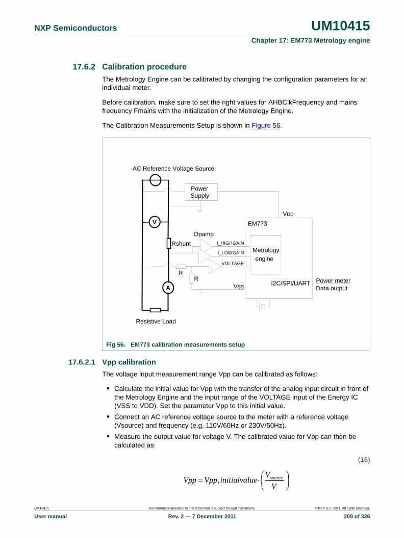
NXP Semiconductors UM10415Chapter 17: EM773 Metrology engine
17.6.2 Calibration procedure
The Metrology Engine can be calibrated by changing the configuration parameters for an individual meter.
Before calibration, make sure to set the right values for AHBClkFrequency and mains frequency Fmains with the initialization of the Metrology Engine.
The Calibration Measurements Setup is shown in Figure 56.
17.6.2.1 Vpp calibration
The voltage input measurement range Vpp can be calibrated as follows:
• Calculate the initial value for Vpp with the transfer of the analog input circuit in front of the Metrology Engine and the input range of the VOLTAGE input of the Energy IC (VSS to VDD). Set the parameter Vpp to this initial value.
• Connect an AC reference voltage source to the meter with a reference voltage (Vsource) and frequency (e.g. 110V/60Hz or 230V/50Hz).
• Measure the output value for voltage V. The calibrated value for Vpp can then be calculated as:
(16)
Fig 56. EM773 calibration measurements setup
AC Reference Voltage Source
Resistive Load
Opamp
Metrology
EM773
Rshunt
RR
VDD
Power
engine
I2C/SPI/UART Power meterData outputVSS
VOLTAGE
I_HIGHGAIN
I_LOWGAIN
Supply
A
V
V
VueinitialvalVppVpp source,
UM10415 All information provided in this document is subject to legal disclaimers. © NXP B.V. 2011. All rights reserved.
User manual Rev. 2 — 7 December 2011 209 of 326

NXP Semiconductors UM10415Chapter 17: EM773 Metrology engine
• Set this new value as Vpp
The calibration can be verified by checking the measured voltage V again. This should now equal Vsource.
17.6.2.2 I1pp calibration
The current input measurement range I1pp can be calibrated as follows:
• Calculate the initial value for I1pp with the transfer of the analog input circuit in front of the Metrology Engine and the input range of the I_HIGHGAIN input of the Energy IC (VSS to VDD). Set the parameter I1pp to this initial value.
• Connect an AC reference voltage source to the meter with a reference voltage and frequency (e.g. 110V/60Hz or 230V/50Hz).
• Connect a reference load with a known current Iref1. Remark: Make sure the current is in the range for I1pp.
• Measure the output value for current I. The calibrated value for I1pp can then be calculated as:
(17)
• Set this new value as I1pp.
The calibration can be verified by checking the measured current I again. This should now equal Iref1.
17.6.2.3 I2pp calibration
The current input measurement range I2pp can be calibrated as follows:
• Calculate the initial value for I2pp with the transfer of the analog input circuit in front of the Metrology Engine and the input range of the I_LOWGAIN input of the Energy IC (VSS to VDD). Set the parameter I2pp to this initial value.
• Connect an AC reference voltage source to the meter with a reference voltage and frequency (e.g. 110V/60Hz or 230V/50Hz).
• Connect a reference load with a known current Iref2. Remark: Make sure the current is in the range for I2pp.
• Measure the output value for current I. The calibrated value for I2pp can then be calculated as:
(18)
• Set this new value as I2pp.
I
IueinitialvalppIppI ref 1,11
I
IueinitialvalppIppI ref 2,22
UM10415 All information provided in this document is subject to legal disclaimers. © NXP B.V. 2011. All rights reserved.
User manual Rev. 2 — 7 December 2011 210 of 326

NXP Semiconductors UM10415Chapter 17: EM773 Metrology engine
The calibration can be verified by checking the measured current I again. This should now equal Iref2.
17.6.2.4 DeltaPhi1 calibration
The phase error correction angle DeltaPhi1 can be calibrated as follows:
• Connect an AC reference voltage source to the meter with the correct voltage and frequency (e.g. 110V/60Hz or 230V/50Hz).
• Set DeltaPhi1 to zero and apply a resistive load (that has no reactive power) to the meter. Remark: Make sure the current is in the range for I1pp.
• Measure the output values for fundamental Reactive Power Q1 and active power P. The correction value DeltaPhi1 can then be calculated as:
(19)
• Set this calculated value as DeltaPhi1.
The calibration can be verified by measuring the fundamental reactive power Q1 for this resistive load again. The fundamental reactive power Q1 should now be reduced towards 0 var for the resistive load.
17.6.2.5 DeltaPhi2 calibration
The phase error correction angle DeltaPhi2 can be calibrated as follows:
• Connect an AC reference voltage source to the meter with the correct voltage and frequency (e.g. 110V/60Hz or 230V/50Hz).
• Set DeltaPhi2 to zero and apply a resistive load (that has no reactive power) to the meter. Remark: Make sure the current is in the range for I2pp.
• Measure the output values for fundamental Reactive Power Q1 and active power P. The correction value DeltaPhi2 can then be calculated as:
(20)
• Set this calculated value as DeltaPhi2.
The calibration can be verified by measuring the fundamental reactive power Q1 for this resistive load again. The fundamental reactive power should now be reduced towards 0 var for the resistive load.
P
QaDeltaPhi 1tan1
P
QaDeltaPhi 1tan2
UM10415 All information provided in this document is subject to legal disclaimers. © NXP B.V. 2011. All rights reserved.
User manual Rev. 2 — 7 December 2011 211 of 326
18.1 How to read this chapter
The EM773 Metrology Engine is available on part EM773 only.
18.2 Metrology driver interface
The following seven interfaces of the metrology firmware are exposed to the user application:
1. metrology engine initialization
2. metrology engine interrupt handler
3. metrology engine set ranges
4. metrology engine start
5. metrology engine stop
6. metrology engine read data
7. metrology engine get gain channel
18.2.1 Metrology Engine initialization
This interface must be called by the application software before the metrology engine can be used.
This interface configures the metrology engine with the proper settings based on the given AHB system frequency and mains frequency.
18.2.2 Metrology Engine interrupt handler
The user application must add the metrology engine interrupt handler to the interrupt vector table. The driver interrupt handler takes appropriate action according the measured data and the configured ranges.
18.2.3 Metrology Engine set ranges
This interface must be called by the application software after the metrology engine is initialized and before the metrology engine is started.
This interface sets the ranges for the voltage input and the current inputs.
The ranges are:
• Vpp for the VOLTAGE input
• I1pp for the I_HIGHGAIN input
• I2pp for the I_LOWGAIN input
• DeltaPhi1 for the I_HIGHGAIN input
• DeltaPhi2 for the I_LOWGAIN input
UM10415Chapter 18: EM773 Metrology engine interfaceRev. 2 — 7 December 2011 User manual
UM10415 All information provided in this document is subject to legal disclaimers. © NXP B.V. 2011. All rights reserved.
User manual Rev. 2 — 7 December 2011 212 of 326
NXP Semiconductors UM10415Chapter 18: EM773 Metrology engine interface
18.2.4 Metrology Engine start
This interface must be called by the application software after the metrology engine is initialized and the ranges are set.
This interface enables the measurements by the metrology engine.
18.2.5 Metrology Engine stop
This interface must be called by the application software after the metrology engine is initialized, the ranges are set and the engine is started.
This interface disables the measurements by the metrology engine.
18.2.6 Metrology Engine read data
This interface can be called by the application software after the metrology engine is initialized, the ranges are set and the engine is started.
This interface returns the measured power readings over the previous second.
The readings are only valid when the interface returns EM_VALID.
Other return values are EM_NOT_VALID (no power reading available) and EM_NOT_VALID_OVERFLOW (no power reading available due to overflow of measurement data).
This interface must be called at least once every second, preferable twice a second, to avoid that measurement data will get lost due to overflow.
18.2.7 Metrology Engine get gain channel
This interface can be called by the application software after the metrology engine is initialized.
This interface returns the currently active current gain input channel, EM_CHANNEL1 for I_HIGHGAIN and EM_CHANNEL2 for I_LOWGAIN.
18.3 Calling the metrology driver
The metrology driver which is supplied as a library (metrology.a) must be linked with the user application.
1. Initialize metrology engine:
metrology_init(12000000, 50);
2. Set ranges for the metrology engine:
metrology_ranges_t metrology_ranges;metrology_ranges.Vpp = (float)954.67;metrology_ranges.I1pp = (float)2.84;metrology_ranges.I2pp = (float)45.60;metrology_ranges.DeltaPhi1 = (float)0.0;metrology_ranges.DeltaPhi2 = (float)0.0;
UM10415 All information provided in this document is subject to legal disclaimers. © NXP B.V. 2011. All rights reserved.
User manual Rev. 2 — 7 December 2011 213 of 326

NXP Semiconductors UM10415Chapter 18: EM773 Metrology engine interface
metrology_set_ranges(&metrology_ranges);
3. Start the metrology engine:
metrology_start();
4. Read the measured data:
while (running){ if (metrology_get_gainchannel() == CURRENT_CHANNEL1) { LED_ON(); /* signal measuring from I_HIGHGAIN */ } else { LED_OFF();/* signal measuring from I_LOWGAIN */ } if (metrology_read_data(&meter_result)) { print_result(&meter_result); } ms_sleep(250);}
5. Stop the metrology engine:
metrology_stop();
18.4 Metrology driver structure definitions
18.4.1 Metrology ranges
The following structure is used to configure the voltage range, current ranges and the phase corrections for the I_HIGHGAIN and I_LOWGAIN gain current channels:
typedef struct metrology_ranges_tag{ float Vpp; float I1pp; float I2pp; float DeltaPhi1; float DeltaPhi2; } metrology_ranges_t;
The metrology ranges class structure is further explained in Table 184 in Section 17.6.1 with the Metrology Engine Configuration parameters.
18.4.2 Metrology result
The following structure is used to pass the measured metrology data over the previous second:
typedef struct metrology_result_tag
UM10415 All information provided in this document is subject to legal disclaimers. © NXP B.V. 2011. All rights reserved.
User manual Rev. 2 — 7 December 2011 214 of 326

NXP Semiconductors UM10415Chapter 18: EM773 Metrology engine interface
{ float V; float I; float P; float Q1; float S; float S1; float PF; float PF1; float SN; float N; float THDI;} metrology_result_t;
The members of the metrology result class structure are explained in Table 185.
Table 185. Metrology result class structure
Member Description
V RMS voltage (in Volt)
I RMS current (in Ampere)
P Active power (in Watt)
Q1 Fundamental reactive power (in var)
S Apparent power (in VA)
S1 Fundamental apparent power (in VA)
PF Power factor (no dimension, 0.00-1.00)
PF1 Fundamental power factor (no dimension, 0.00-1.00)
SN Nonfundamental apparent power (in VA)
N Nonactive power (in var)
THDI Total harmonic distortion of the current (no dimension)
UM10415 All information provided in this document is subject to legal disclaimers. © NXP B.V. 2011. All rights reserved.
User manual Rev. 2 — 7 December 2011 215 of 326

19.1 Features
• In-System Programming: In-System programming (ISP) is programming or reprogramming the on-chip flash memory, using the boot loader software and UART serial port. This can be done when the part resides in the end-user board.
• In-Application Programming: In-Application (IAP) programming is performing erase and write operation on the on-chip flash memory, as directed by the end-user application code.
• Flash access times can be configured through a register in the flash controller block.
• Erase time for one sector is 100 ms ± 5%. Programming time for one block of 256 bytes is 1 ms ± 5%.
19.2 General description
19.2.1 Boot loader
The boot loader controls initial operation after reset and also provides the means to accomplish programming of the flash memory via UART. This could be initial programming of a blank device, erasure and re-programming of a previously programmed device, or programming of the flash memory by the application program in a running system.
The boot loader code is executed every time the part is powered on or reset. The loader can execute the ISP command handler or the user application code. A LOW level after reset at the PIO0_1 pin is considered as an external hardware request to start the ISP command handler via UART.
Assuming that power supply pins are on their nominal levels when the rising edge on RESET pin is generated, it may take up to 3 ms before PIO0_1 is sampled and the decision on whether to continue with user code or ISP handler is made. If PIO0_1 is sampled low and the watchdog overflow flag is set, the external hardware request to start the ISP command handler is ignored. If there is no request for the ISP command handler execution (PIO0_1 is sampled HIGH after reset), a search is made for a valid user program. If a valid user program is found then the execution control is transferred to it. If a valid user program is not found, the auto-baud routine is invoked.
Remark: The sampling of pin PIO0_1 can be disabled through programming flash location 0x0000 02FC (see Section 19.2.7.1).
19.2.2 Memory map after any reset
The boot block is 16 kB in size. The boot block is located in the memory region starting from the address 0x1FFF 0000. The boot loader is designed to run from this memory area, but both the ISP and IAP software use parts of the on-chip RAM. The RAM usage is described later in this chapter. The interrupt vectors residing in the boot block of the on-chip flash memory also become active after reset, i.e., the bottom 512 bytes of the boot block are also visible in the memory region starting from the address 0x0000 0000.
UM10415Chapter 19: EM773 Flash memory programming firmwareRev. 2 — 7 December 2011 User manual
UM10415 All information provided in this document is subject to legal disclaimers. © NXP B.V. 2011. All rights reserved.
User manual Rev. 2 — 7 December 2011 216 of 326

NXP Semiconductors UM10415Chapter 19: EM773 Flash memory programming firmware
19.2.3 Criterion for Valid User Code
Criterion for valid user code: The reserved Cortex-M0 exception vector location 7 (offset 0x 0000 001C in the vector table) should contain the 2’s complement of the check-sum of table entries 0 through 6. This causes the checksum of the first 8 table entries to be 0. The boot loader code checksums the first 8 locations in sector 0 of the flash. If the result is 0, then execution control is transferred to the user code.
If the signature is not valid, the auto-baud routine synchronizes with the host via serial port 0. The host should send a ‘?’ (0x3F) as a synchronization character and wait for a response. The host side serial port settings should be 8 data bits, 1 stop bit and no parity. The auto-baud routine measures the bit time of the received synchronization character in terms of its own frequency and programs the baud rate generator of the serial port. It also sends an ASCII string ("Synchronized<CR><LF>") to the Host. In response to this host should send the same string ("Synchronized<CR><LF>"). The auto-baud routine looks at the received characters to verify synchronization. If synchronization is verified then "OK<CR><LF>" string is sent to the host. Host should respond by sending the crystal frequency (in kHz) at which the part is running. For example, if the part is running at 10 MHz, the response from the host should be "10000<CR><LF>". "OK<CR><LF>" string is sent to the host after receiving the crystal frequency. If synchronization is not verified then the auto-baud routine waits again for a synchronization character. For auto-baud to work correctly in case of user invoked ISP, the CCLK frequency should be greater than or equal to 10 MHz.
Once the crystal frequency is received the part is initialized and the ISP command handler is invoked. For safety reasons an "Unlock" command is required before executing the commands resulting in flash erase/write operations and the "Go" command. The rest of the commands can be executed without the unlock command. The Unlock command is required to be executed once per ISP session. The Unlock command is explained in Section 19.4 “UART ISP commands” on page 223.
UM10415 All information provided in this document is subject to legal disclaimers. © NXP B.V. 2011. All rights reserved.
User manual Rev. 2 — 7 December 2011 217 of 326

NXP Semiconductors UM10415Chapter 19: EM773 Flash memory programming firmware
19.2.4 Boot process flowchart
19.2.5 Sector numbers
Some IAP and ISP commands operate on sectors and specify sector numbers. The following table shows the correspondence between sector numbers and memory addresses for the EM773 device.
(1) For details on handling the crystal frequency, see Section 19.5.8 “Reinvoke ISP (IAP)” on page 235
Fig 57. Boot process flowchart
RESET
INITIALIZE
RECEIVE CRYSTAL FREQUENCY
RUN UART ISP COMMAND HANDLER
RUN AUTO-BAUD
CRP1/2/3ENABLED?
WATCHDOGFLAG SET?
CRP3/NO_ISPENABLED?
ENTER ISPMODE?
(PIO0_12 = LOW)
USER CODEVALID?
USER CODEVALID?
AUTO-BAUDSUCCESSFUL?
EXECUTE INTERNALUSER CODE
ENABLE DEBUG
yes
yes
yes
yes
yes
yes
yes
no
no
no
no
nono
no
no
A
A
UM10415 All information provided in this document is subject to legal disclaimers. © NXP B.V. 2011. All rights reserved.
User manual Rev. 2 — 7 December 2011 218 of 326

NXP Semiconductors UM10415Chapter 19: EM773 Flash memory programming firmware
19.2.6 Flash content protection mechanism
The EM773 is equipped with the Error Correction Code (ECC) capable Flash memory. The purpose of an error correction module is twofold. Firstly, it decodes data words read from the memory into output data words. Secondly, it encodes data words to be written to the memory. The error correction capability consists of single bit error correction with Hamming code.
The operation of ECC is transparent to the running application. The ECC content itself is stored in a flash memory not accessible by user’s code to either read from it or write into it on its own. A byte of ECC corresponds to every consecutive 128 bits of the user accessible Flash. Consequently, Flash bytes from 0x0000 0000 to 0x0000 000F are protected by the first ECC byte, Flash bytes from 0x0000 0010 to 0x0000 001F are protected by the second ECC byte, etc.
Whenever the CPU requests a read from user’s Flash, both 128 bits of raw data containing the specified memory location and the matching ECC byte are evaluated. If the ECC mechanism detects a single error in the fetched data, a correction will be applied before data are provided to the CPU. When a write request into the user’s Flash is made, write of user specified content is accompanied by a matching ECC value calculated and stored in the ECC memory.
When a sector of Flash memory is erased, the corresponding ECC bytes are also erased. Once an ECC byte is written, it can not be updated unless it is erased first. Therefore, for the implemented ECC mechanism to perform properly, data must be written into the flash memory in groups of 16 bytes (or multiples of 16), aligned as described above.
19.2.7 Code Read Protection (CRP)
Code Read Protection is a mechanism that allows the user to enable different levels of security in the system so that access to the on-chip flash and use of the ISP can be restricted. When needed, CRP is invoked by programming a specific pattern in flash location at 0x0000 02FC. IAP commands are not affected by the code read protection.
Important: any CRP change becomes effective only after the device has gone through a power cycle.
Table 186. Flash sector configuration
Sectornumber
Sector size Address range EM77332 kB flash
0 4 kB 0x0000 0000 - 0x0000 0FFF yes
1 4 kB 0x0000 1000 - 0x0000 1FFF yes
2 4 kB 0x0000 2000 - 0x0000 2FFF yes
3 4 kB 0x0000 3000 - 0x0000 3FFF yes
4 4 kB 0x0000 4000 - 0x0000 4FFF yes
5 4 kB 0x0000 5000 - 0x0000 5FFF yes
6 4 kB 0x0000 6000 - 0x0000 6FFF yes
7 4 kB 0x0000 7000 - 0x0000 7FFF yes
UM10415 All information provided in this document is subject to legal disclaimers. © NXP B.V. 2011. All rights reserved.
User manual Rev. 2 — 7 December 2011 219 of 326

NXP Semiconductors UM10415Chapter 19: EM773 Flash memory programming firmware
Table 187. Code Read Protection options
Name Pattern programmed in 0x0000 02FC
Description
NO_ISP 0x4E69 7370 Prevents sampling of pin PIO0_1 for entering ISP mode. PIO0_1 is available for other uses.
CRP1 0x12345678 Access to chip via the SWD pins is disabled. This mode allows partial flash update using the following ISP commands and restrictions:
• Write to RAM command should not access RAM below 0x1000 0300. Access to addresses below 0x1000 0200 is disabled.
• Copy RAM to flash command can not write to Sector 0.
• Erase command can erase Sector 0 only when all sectors are selected for erase.
• Compare command is disabled.
• Read Memory command is disabled.
This mode is useful when CRP is required and flash field updates are needed but all sectors can not be erased. Since compare command is disabled in case of partial updates the secondary loader should implement checksum mechanism to verify the integrity of the flash.
CRP2 0x87654321 Access to chip via the SWD pins is disabled. The following ISP commands are disabled:
• Read Memory
• Write to RAM
• Go
• Copy RAM to flash
• Compare
When CRP2 is enabled the ISP erase command only allows erasure of all user sectors.
CRP3 0x43218765 Access to chip via the SWD pins is disabled. ISP entry by pulling PIO0_1 LOW is disabled if a valid user code is present in flash sector 0.
This mode effectively disables ISP override using PIO0_1 pin. It is up to the user’s application to provide a flash update mechanism using IAP calls or call reinvoke ISP command to enable flash update via UART.
Caution: If CRP3 is selected, no future factory testing can be performed on the device.
Table 188. Code Read Protection hardware/software interaction
CRP option User Code Valid
PIO0_1 pin at reset
SWD enabled EM773 enters ISP mode
partial flash update in ISP mode
No No x Yes Yes Yes
No Yes High Yes No NA
No Yes Low Yes Yes Yes
CRP1 Yes High No No NA
CRP1 Yes Low No Yes Yes
CRP2 Yes High No No NA
CRP2 Yes Low No Yes No
UM10415 All information provided in this document is subject to legal disclaimers. © NXP B.V. 2011. All rights reserved.
User manual Rev. 2 — 7 December 2011 220 of 326
NXP Semiconductors UM10415Chapter 19: EM773 Flash memory programming firmware
In case a CRP mode is enabled and access to the chip is allowed via the ISP, an unsupported or restricted ISP command will be terminated with return code CODE_READ_PROTECTION_ENABLED.
19.2.7.1 ISP entry protection
In addition to the three CRP modes, the user can prevent the sampling of pin PIO0_1 for entering ISP mode and thereby release pin PIO0_1 for other uses. This is called the NO_ISP mode. The NO_ISP mode can be entered by programming the pattern 0x4E69 7370 at location 0x0000 02FC.
19.3 UART Communication protocol
All UART ISP commands should be sent as single ASCII strings. Strings should be terminated with Carriage Return (CR) and/or Line Feed (LF) control characters. Extra <CR> and <LF> characters are ignored. All ISP responses are sent as <CR><LF> terminated ASCII strings. Data is sent and received in UU-encoded format.
CRP3 Yes x No No NA
CRP1 No x No Yes Yes
CRP2 No x No Yes No
CRP3 No x No Yes No
Table 189. ISP commands allowed for different CRP levels
ISP command CRP1 CRP2 CRP3 (no entry in ISP mode allowed)
Unlock yes yes n/a
Set Baud Rate yes yes n/a
Echo yes yes n/a
Write to RAM yes; above 0x1000 0300 only
no n/a
Read Memory no no n/a
Prepare sector(s) for write operation
yes yes n/a
Copy RAM to flash yes; not to sector 0 no n/a
Go no no n/a
Erase sector(s) yes; sector 0 can only be erased when all sectors are erased.
yes; all sectors only
n/a
Blank check sector(s) no no n/a
Read Part ID yes yes n/a
Read Boot code version yes yes n/a
Compare no no n/a
ReadUID yes yes n/a
Table 188. Code Read Protection hardware/software interaction …continued
CRP option User Code Valid
PIO0_1 pin at reset
SWD enabled EM773 enters ISP mode
partial flash update in ISP mode
UM10415 All information provided in this document is subject to legal disclaimers. © NXP B.V. 2011. All rights reserved.
User manual Rev. 2 — 7 December 2011 221 of 326
NXP Semiconductors UM10415Chapter 19: EM773 Flash memory programming firmware
19.3.1 UART ISP command format
"Command Parameter_0 Parameter_1 ... Parameter_n<CR><LF>" "Data" (Data only for Write commands).
19.3.2 UART ISP response format
"Return_Code<CR><LF>Response_0<CR><LF>Response_1<CR><LF> ... Response_n<CR><LF>" "Data" (Data only for Read commands).
19.3.3 UART ISP data format
The data stream is in UU-encode format. The UU-encode algorithm converts 3 bytes of binary data in to 4 bytes of printable ASCII character set. It is more efficient than Hex format which converts 1 byte of binary data in to 2 bytes of ASCII hex. The sender should send the check-sum after transmitting 20 UU-encoded lines. The length of any UU-encoded line should not exceed 61 characters(bytes) i.e. it can hold 45 data bytes. The receiver should compare it with the check-sum of the received bytes. If the check-sum matches then the receiver should respond with "OK<CR><LF>" to continue further transmission. If the check-sum does not match the receiver should respond with "RESEND<CR><LF>". In response the sender should retransmit the bytes.
A description of UU-encode is available at the wotsit webpage.
19.3.4 UART ISP flow control
A software XON/XOFF flow control scheme is used to prevent data loss due to buffer overrun. When the data arrives rapidly, the ASCII control character DC3 (stop) is sent to stop the flow of data. Data flow is resumed by sending the ASCII control character DC1 (start). The host should also support the same flow control scheme.
19.3.5 UART SP command abort
Commands can be aborted by sending the ASCII control character "ESC". This feature is not documented as a command under "ISP Commands" section. Once the escape code is received the ISP command handler waits for a new command.
19.3.6 Interrupts during UART ISP
The boot block interrupt vectors located in the boot block of the flash are active after any reset.
19.3.7 Interrupts during IAP
The on-chip flash memory is not accessible during erase/write operations. When the user application code starts executing the interrupt vectors from the user flash area are active. The user should either disable interrupts, or ensure that user interrupt vectors are active in RAM and that the interrupt handlers reside in RAM, before making a flash erase/write IAP call. The IAP code does not use or disable interrupts.
UM10415 All information provided in this document is subject to legal disclaimers. © NXP B.V. 2011. All rights reserved.
User manual Rev. 2 — 7 December 2011 222 of 326

NXP Semiconductors UM10415Chapter 19: EM773 Flash memory programming firmware
19.3.8 RAM used by ISP command handler
ISP commands use on-chip RAM from 0x1000 017C to 0x1000 025B. The user could use this area, but the contents may be lost upon reset. Flash programming commands use the top 32 bytes of on-chip RAM. The stack is located at (RAM top 32). The maximum stack usage is 256 bytes and it grows downwards.
19.3.9 RAM used by IAP command handler
Flash programming commands use the top 32 bytes of on-chip RAM. The maximum stack usage in the user allocated stack space is 128 bytes and it grows downwards.
19.4 UART ISP commands
The following commands are accepted by the ISP command handler. Detailed status codes are supported for each command. The command handler sends the return code INVALID_COMMAND when an undefined command is received. Commands and return codes are in ASCII format.
CMD_SUCCESS is sent by ISP command handler only when received ISP command has been completely executed and the new ISP command can be given by the host. Exceptions from this rule are "Set Baud Rate", "Write to RAM", "Read Memory", and "Go" commands.
Table 190. UART ISP command summary
ISP Command Usage Described in
Unlock U <Unlock Code> Table 191
Set Baud Rate B <Baud Rate> <stop bit> Table 192
Echo A <setting> Table 193
Write to RAM W <start address> <number of bytes> Table 194
Read Memory R <address> <number of bytes> Table 195
Prepare sector(s) for write operation
P <start sector number> <end sector number> Table 196
Copy RAM to flash C <Flash address> <RAM address> <number of bytes> Table 197
Go G <address> <Mode> Table 198
Erase sector(s) E <start sector number> <end sector number> Table 199
Blank check sector(s) I <start sector number> <end sector number> Table 200
Read Part ID J Table 201
Read Boot code version K Table 203
Compare M <address1> <address2> <number of bytes> Table 204
ReadUID N Table 205
UM10415 All information provided in this document is subject to legal disclaimers. © NXP B.V. 2011. All rights reserved.
User manual Rev. 2 — 7 December 2011 223 of 326

NXP Semiconductors UM10415Chapter 19: EM773 Flash memory programming firmware
19.4.1 Unlock <Unlock code> (UART ISP)
19.4.2 Set Baud Rate <Baud Rate> <stop bit> (UART ISP)
19.4.3 Echo <setting> (UART ISP)
19.4.4 Write to RAM <start address> <number of bytes> (UART ISP)
The host should send the data only after receiving the CMD_SUCCESS return code. The host should send the check-sum after transmitting 20 UU-encoded lines. The checksum is generated by adding raw data (before UU-encoding) bytes and is reset after transmitting 20 UU-encoded lines. The length of any UU-encoded line should not exceed 61 characters(bytes) i.e. it can hold 45 data bytes. When the data fits in less then 20 UU-encoded lines then the check-sum should be of the actual number of bytes sent. The ISP command handler compares it with the check-sum of the received bytes. If the check-sum matches, the ISP command handler responds with "OK<CR><LF>" to
Table 191. UART ISP Unlock command
Command U
Input Unlock code: 2313010
Return Code CMD_SUCCESS |
INVALID_CODE |
PARAM_ERROR
Description This command is used to unlock Flash Write, Erase, and Go commands.
Example "U 23130<CR><LF>" unlocks the Flash Write/Erase & Go commands.
Table 192. UART ISP Set Baud Rate command
Command B
Input Baud Rate: 9600 | 19200 | 38400 | 57600 | 115200 | 230400
Stop bit: 1 | 2
Return Code CMD_SUCCESS |
INVALID_BAUD_RATE |
INVALID_STOP_BIT |
PARAM_ERROR
Description This command is used to change the baud rate. The new baud rate is effective after the command handler sends the CMD_SUCCESS return code.
Example "B 57600 1<CR><LF>" sets the serial port to baud rate 57600 bps and 1 stop bit.
Table 193. UART ISP Echo command
Command A
Input Setting: ON = 1 | OFF = 0
Return Code CMD_SUCCESS |
PARAM_ERROR
Description The default setting for echo command is ON. When ON the ISP command handler sends the received serial data back to the host.
Example "A 0<CR><LF>" turns echo off.
UM10415 All information provided in this document is subject to legal disclaimers. © NXP B.V. 2011. All rights reserved.
User manual Rev. 2 — 7 December 2011 224 of 326
NXP Semiconductors UM10415Chapter 19: EM773 Flash memory programming firmware
continue further transmission. If the check-sum does not match, the ISP command handler responds with "RESEND<CR><LF>". In response the host should retransmit the bytes.
19.4.5 Read Memory <address> <no. of bytes> (UART ISP)
The data stream is followed by the command success return code. The check-sum is sent after transmitting 20 UU-encoded lines. The checksum is generated by adding raw data (before UU-encoding) bytes and is reset after transmitting 20 UU-encoded lines. The length of any UU-encoded line should not exceed 61 characters(bytes) i.e. it can hold 45 data bytes. When the data fits in less then 20 UU-encoded lines then the check-sum is of actual number of bytes sent. The host should compare it with the checksum of the received bytes. If the check-sum matches then the host should respond with "OK<CR><LF>" to continue further transmission. If the check-sum does not match then the host should respond with "RESEND<CR><LF>". In response the ISP command handler sends the data again.
Table 194. UART ISP Write to RAM command
Command W
Input Start Address: RAM address where data bytes are to be written. This address should be a word boundary.
Number of Bytes: Number of bytes to be written. Count should be a multiple of 4
Return Code CMD_SUCCESS |
ADDR_ERROR (Address not on word boundary) |
ADDR_NOT_MAPPED |
COUNT_ERROR (Byte count is not multiple of 4) |
PARAM_ERROR |
CODE_READ_PROTECTION_ENABLED
Description This command is used to download data to RAM. Data should be in UU-encoded format. This command is blocked when code read protection is enabled.
Example "W 268436224 4<CR><LF>" writes 4 bytes of data to address 0x1000 0300.
Table 195. UART ISP Read Memory command
Command R
Input Start Address: Address from where data bytes are to be read. This address should be a word boundary.
Number of Bytes: Number of bytes to be read. Count should be a multiple of 4.
Return Code CMD_SUCCESS followed by <actual data (UU-encoded)> |
ADDR_ERROR (Address not on word boundary) |
ADDR_NOT_MAPPED |
COUNT_ERROR (Byte count is not a multiple of 4) |
PARAM_ERROR |
CODE_READ_PROTECTION_ENABLED
Description This command is used to read data from RAM or flash memory. This command is blocked when code read protection is enabled.
Example "R 268435456 4<CR><LF>" reads 4 bytes of data from address 0x1000 0000.
UM10415 All information provided in this document is subject to legal disclaimers. © NXP B.V. 2011. All rights reserved.
User manual Rev. 2 — 7 December 2011 225 of 326
NXP Semiconductors UM10415Chapter 19: EM773 Flash memory programming firmware
19.4.6 Prepare sector(s) for write operation <start sector number> <end sector number> (UART ISP)
This command makes flash write/erase operation a two step process.
19.4.7 Copy RAM to flash <Flash address> <RAM address> <no of bytes> (UART ISP)
Table 196. UART ISP Prepare sector(s) for write operation command
Command P
Input Start Sector Number
End Sector Number: Should be greater than or equal to start sector number.
Return Code CMD_SUCCESS |
BUSY |
INVALID_SECTOR |
PARAM_ERROR
Description This command must be executed before executing "Copy RAM to flash" or "Erase Sector(s)" command. Successful execution of the "Copy RAM to flash" or "Erase Sector(s)" command causes relevant sectors to be protected again. The boot block can not be prepared by this command. To prepare a single sector use the same "Start" and "End" sector numbers.
Example "P 0 0<CR><LF>" prepares the flash sector 0.
Table 197. UART ISP Copy command
Command C
Input Flash Address(DST): Destination flash address where data bytes are to be written. The destination address should be a 256 byte boundary.
RAM Address(SRC): Source RAM address from where data bytes are to be read.
Number of Bytes: Number of bytes to be written. Should be 256 | 512 | 1024 | 4096.
Return Code CMD_SUCCESS |
SRC_ADDR_ERROR (Address not on word boundary) |
DST_ADDR_ERROR (Address not on correct boundary) |
SRC_ADDR_NOT_MAPPED |
DST_ADDR_NOT_MAPPED |
COUNT_ERROR (Byte count is not 256 | 512 | 1024 | 4096) |
SECTOR_NOT_PREPARED_FOR WRITE_OPERATION |
BUSY |
CMD_LOCKED |
PARAM_ERROR |
CODE_READ_PROTECTION_ENABLED
Description This command is used to program the flash memory. The "Prepare Sector(s) for Write Operation" command should precede this command. The affected sectors are automatically protected again once the copy command is successfully executed. The boot block cannot be written by this command. This command is blocked when code read protection is enabled.
Example "C 0 268467504 512<CR><LF>" copies 512 bytes from the RAM address 0x1000 0800 to the flash address 0.
UM10415 All information provided in this document is subject to legal disclaimers. © NXP B.V. 2011. All rights reserved.
User manual Rev. 2 — 7 December 2011 226 of 326

NXP Semiconductors UM10415Chapter 19: EM773 Flash memory programming firmware
19.4.8 Go <address> <mode> (UART ISP)
19.4.9 Erase sector(s) <start sector number> <end sector number> (UART ISP)
Table 198. UART ISP Go command
Command G
Input Address: Flash or RAM address from which the code execution is to be started. This address should be on a word boundary.
Mode: T (Execute program in Thumb Mode) | A (Execute program in ARM mode).
Return Code CMD_SUCCESS |
ADDR_ERROR |
ADDR_NOT_MAPPED |
CMD_LOCKED |
PARAM_ERROR |
CODE_READ_PROTECTION_ENABLED
Description This command is used to execute a program residing in RAM or flash memory. It may not be possible to return to the ISP command handler once this command is successfully executed. This command is blocked when code read protection is enabled. The command must be used with an address of 0x0000 0200 or greater.
Example "G 512 T<CR><LF>" branches to address 0x0000 0200 in Thumb mode.
Table 199. UART ISP Erase sector command
Command E
Input Start Sector Number
End Sector Number: Should be greater than or equal to start sector number.
Return Code CMD_SUCCESS |
BUSY |
INVALID_SECTOR |
SECTOR_NOT_PREPARED_FOR_WRITE_OPERATION |
CMD_LOCKED |
PARAM_ERROR |
CODE_READ_PROTECTION_ENABLED
Description This command is used to erase one or more sector(s) of on-chip flash memory. The boot block can not be erased using this command. This command only allows erasure of all user sectors when the code read protection is enabled.
Example "E 2 3<CR><LF>" erases the flash sectors 2 and 3.
UM10415 All information provided in this document is subject to legal disclaimers. © NXP B.V. 2011. All rights reserved.
User manual Rev. 2 — 7 December 2011 227 of 326

NXP Semiconductors UM10415Chapter 19: EM773 Flash memory programming firmware
19.4.10 Blank check sector(s) <sector number> <end sector number> (UART ISP)
19.4.11 Read Part Identification number (UART ISP)
19.4.12 Read Boot code version number (UART ISP)
Table 200. UART ISP Blank check sector command
Command I
Input Start Sector Number:
End Sector Number: Should be greater than or equal to start sector number.
Return Code CMD_SUCCESS |
SECTOR_NOT_BLANK (followed by <Offset of the first non blank word location> <Contents of non blank word location>) |
INVALID_SECTOR |
PARAM_ERROR |
Description This command is used to blank check one or more sectors of on-chip flash memory.
Blank check on sector 0 always fails as first 64 bytes are re-mapped to flash boot block.
When CRP is enabled, the blank check command returns 0 for the offset and value of sectors which are not blank. Blank sectors are correctly reported irrespective of the CRP setting.
Example "I 2 3<CR><LF>" blank checks the flash sectors 2 and 3.
Table 201. UART ISP Read Part Identification command
Command J
Input None.
Return Code CMD_SUCCESS followed by part identification number in ASCII (see Table 202 “EM773 part identification numbers”).
Description This command is used to read the part identification number.
Table 202. EM773 part identification numbers
Device ASCII/dec coding Hex coding
EM773FHN33/301 71569451 0x0444 102B
EM773FHN33/302 624955435 0x2540 102B
Table 203. UART ISP Read Boot Code version number command
Command K
Input None
Return Code CMD_SUCCESS followed by 2 bytes of boot code version number in ASCII format. It is to be interpreted as <byte1(Major)>.<byte0(Minor)>.
Description This command is used to read the boot code version number.
UM10415 All information provided in this document is subject to legal disclaimers. © NXP B.V. 2011. All rights reserved.
User manual Rev. 2 — 7 December 2011 228 of 326

NXP Semiconductors UM10415Chapter 19: EM773 Flash memory programming firmware
19.4.13 Compare <address1> <address2> <no of bytes> (UART ISP)
19.4.14 ReadUID (UART ISP)
19.4.15 UART ISP Return Codes
Table 204. UART ISP Compare command
Command M
Input Address1 (DST): Starting flash or RAM address of data bytes to be compared. This address should be a word boundary.
Address2 (SRC): Starting flash or RAM address of data bytes to be compared. This address should be a word boundary.
Number of Bytes: Number of bytes to be compared; should be a multiple of 4.
Return Code CMD_SUCCESS | (Source and destination data are equal)
COMPARE_ERROR | (Followed by the offset of first mismatch)
COUNT_ERROR (Byte count is not a multiple of 4) |
ADDR_ERROR |
ADDR_NOT_MAPPED |
PARAM_ERROR |
Description This command is used to compare the memory contents at two locations.
Compare result may not be correct when source or destination address contains any of the first 512 bytes starting from address zero. First 512 bytes are re-mapped to boot ROM
Example "M 8192 268468224 4<CR><LF>" compares 4 bytes from the RAM address 0x1000 8000 to the 4 bytes from the flash address 0x2000.
Table 205. UART ISP ReadUID command
Command N
Input None
Return Code CMD_SUCCESS followed by four 32-bit words of E-sort test information in ASCII format. The word sent at the lowest address is sent first.
Description This command is used to read the unique ID.
Table 206. UART ISP Return Codes Summary
Return Code
Mnemonic Description
0 CMD_SUCCESS Command is executed successfully. Sent by ISP handler only when command given by the host has been completely and successfully executed.
1 INVALID_COMMAND Invalid command.
2 SRC_ADDR_ERROR Source address is not on word boundary.
3 DST_ADDR_ERROR Destination address is not on a correct boundary.
4 SRC_ADDR_NOT_MAPPED Source address is not mapped in the memory map. Count value is taken in to consideration where applicable.
5 DST_ADDR_NOT_MAPPED Destination address is not mapped in the memory map. Count value is taken in to consideration where applicable.
UM10415 All information provided in this document is subject to legal disclaimers. © NXP B.V. 2011. All rights reserved.
User manual Rev. 2 — 7 December 2011 229 of 326
NXP Semiconductors UM10415Chapter 19: EM773 Flash memory programming firmware
19.5 IAP commands
For in application programming the IAP routine should be called with a word pointer in register r0 pointing to memory (RAM) containing command code and parameters. Result of the IAP command is returned in the result table pointed to by register r1. The user can reuse the command table for result by passing the same pointer in registers r0 and r1. The parameter table should be big enough to hold all the results in case if number of results are more than number of parameters. Parameter passing is illustrated in the Figure 58. The number of parameters and results vary according to the IAP command. The maximum number of parameters is 5, passed to the "Copy RAM to FLASH" command. The maximum number of results is 4, returned by the "ReadUID" command. The command handler sends the status code INVALID_COMMAND when an undefined command is received. The IAP routine resides at 0x1FFF 1FF0 location and it is thumb code.
The IAP function could be called in the following way using C.
Define the IAP location entry point. Since the 0th bit of the IAP location is set there will be a change to Thumb instruction set when the program counter branches to this address.
#define IAP_LOCATION 0x1fff1ff1
Define data structure or pointers to pass IAP command table and result table to the IAP function:
unsigned long command[5];
6 COUNT_ERROR Byte count is not multiple of 4 or is not a permitted value.
7 INVALID_SECTOR Sector number is invalid or end sector number is greater than start sector number.
8 SECTOR_NOT_BLANK Sector is not blank.
9 SECTOR_NOT_PREPARED_FOR_WRITE_OPERATION
Command to prepare sector for write operation was not executed.
10 COMPARE_ERROR Source and destination data not equal.
11 BUSY Flash programming hardware interface is busy.
12 PARAM_ERROR Insufficient number of parameters or invalid parameter.
13 ADDR_ERROR Address is not on word boundary.
14 ADDR_NOT_MAPPED Address is not mapped in the memory map. Count value is taken in to consideration where applicable.
15 CMD_LOCKED Command is locked.
16 INVALID_CODE Unlock code is invalid.
17 INVALID_BAUD_RATE Invalid baud rate setting.
18 INVALID_STOP_BIT Invalid stop bit setting.
19 CODE_READ_PROTECTION_ENABLED
Code read protection enabled.
Table 206. UART ISP Return Codes Summary
Return Code
Mnemonic Description
UM10415 All information provided in this document is subject to legal disclaimers. © NXP B.V. 2011. All rights reserved.
User manual Rev. 2 — 7 December 2011 230 of 326
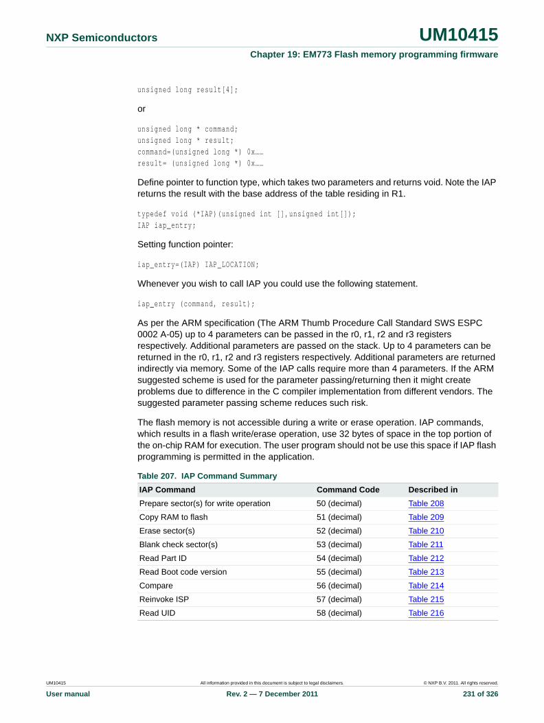
NXP Semiconductors UM10415Chapter 19: EM773 Flash memory programming firmware
unsigned long result[4];
or
unsigned long * command;unsigned long * result;command=(unsigned long *) 0x……result= (unsigned long *) 0x……
Define pointer to function type, which takes two parameters and returns void. Note the IAP returns the result with the base address of the table residing in R1.
typedef void (*IAP)(unsigned int [],unsigned int[]);IAP iap_entry;
Setting function pointer:
iap_entry=(IAP) IAP_LOCATION;
Whenever you wish to call IAP you could use the following statement.
iap_entry (command, result);
As per the ARM specification (The ARM Thumb Procedure Call Standard SWS ESPC 0002 A-05) up to 4 parameters can be passed in the r0, r1, r2 and r3 registers respectively. Additional parameters are passed on the stack. Up to 4 parameters can be returned in the r0, r1, r2 and r3 registers respectively. Additional parameters are returned indirectly via memory. Some of the IAP calls require more than 4 parameters. If the ARM suggested scheme is used for the parameter passing/returning then it might create problems due to difference in the C compiler implementation from different vendors. The suggested parameter passing scheme reduces such risk.
The flash memory is not accessible during a write or erase operation. IAP commands, which results in a flash write/erase operation, use 32 bytes of space in the top portion of the on-chip RAM for execution. The user program should not be use this space if IAP flash programming is permitted in the application.
Table 207. IAP Command Summary
IAP Command Command Code Described in
Prepare sector(s) for write operation 50 (decimal) Table 208
Copy RAM to flash 51 (decimal) Table 209
Erase sector(s) 52 (decimal) Table 210
Blank check sector(s) 53 (decimal) Table 211
Read Part ID 54 (decimal) Table 212
Read Boot code version 55 (decimal) Table 213
Compare 56 (decimal) Table 214
Reinvoke ISP 57 (decimal) Table 215
Read UID 58 (decimal) Table 216
UM10415 All information provided in this document is subject to legal disclaimers. © NXP B.V. 2011. All rights reserved.
User manual Rev. 2 — 7 December 2011 231 of 326

NXP Semiconductors UM10415Chapter 19: EM773 Flash memory programming firmware
19.5.1 Prepare sector(s) for write operation (IAP)
This command makes flash write/erase operation a two step process.
Fig 58. IAP parameter passing
COMMAND CODE
PARAMETER 1
PARAMETER 2
PARAMETER n
STATUS CODE
RESULT 1
RESULT 2
RESULT n
commandparameter table
commandresult table
ARM REGISTER r0
ARM REGISTER r1
Table 208. IAP Prepare sector(s) for write operation command
Command Prepare sector(s) for write operation
Input Command code: 50 (decimal)
Param0: Start Sector Number
Param1: End Sector Number (should be greater than or equal to start sector number).
Return Code CMD_SUCCESS |
BUSY |
INVALID_SECTOR
Result None
Description This command must be executed before executing "Copy RAM to flash" or "Erase Sector(s)" command. Successful execution of the "Copy RAM to flash" or "Erase Sector(s)" command causes relevant sectors to be protected again. The boot sector can not be prepared by this command. To prepare a single sector use the same "Start" and "End" sector numbers.
UM10415 All information provided in this document is subject to legal disclaimers. © NXP B.V. 2011. All rights reserved.
User manual Rev. 2 — 7 December 2011 232 of 326
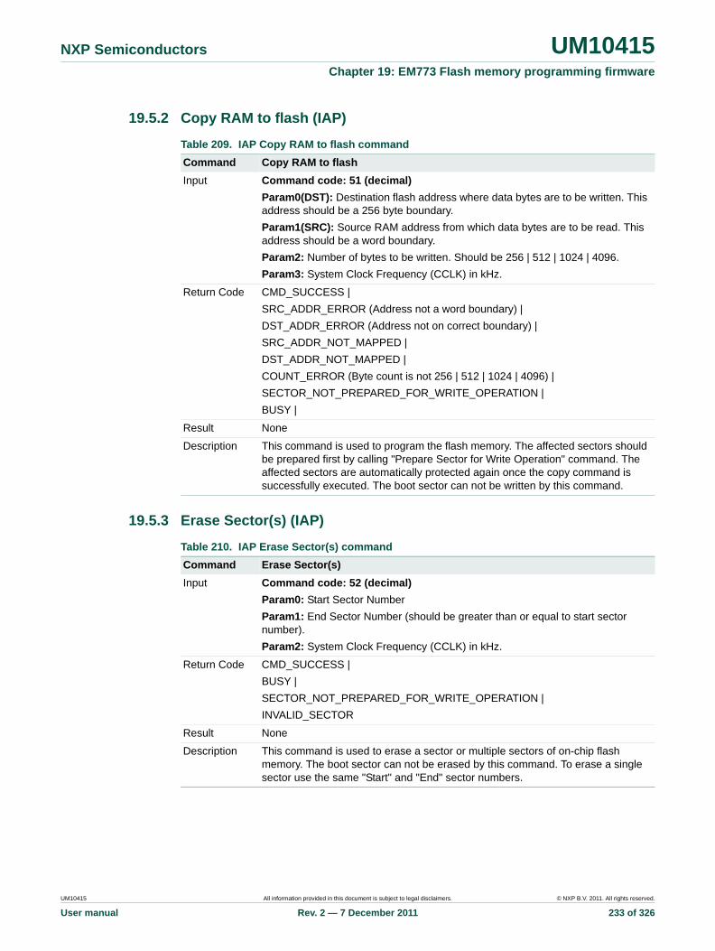
NXP Semiconductors UM10415Chapter 19: EM773 Flash memory programming firmware
19.5.2 Copy RAM to flash (IAP)
19.5.3 Erase Sector(s) (IAP)
Table 209. IAP Copy RAM to flash command
Command Copy RAM to flash
Input Command code: 51 (decimal)
Param0(DST): Destination flash address where data bytes are to be written. This address should be a 256 byte boundary.
Param1(SRC): Source RAM address from which data bytes are to be read. This address should be a word boundary.
Param2: Number of bytes to be written. Should be 256 | 512 | 1024 | 4096.
Param3: System Clock Frequency (CCLK) in kHz.
Return Code CMD_SUCCESS |
SRC_ADDR_ERROR (Address not a word boundary) |
DST_ADDR_ERROR (Address not on correct boundary) |
SRC_ADDR_NOT_MAPPED |
DST_ADDR_NOT_MAPPED |
COUNT_ERROR (Byte count is not 256 | 512 | 1024 | 4096) |
SECTOR_NOT_PREPARED_FOR_WRITE_OPERATION |
BUSY |
Result None
Description This command is used to program the flash memory. The affected sectors should be prepared first by calling "Prepare Sector for Write Operation" command. The affected sectors are automatically protected again once the copy command is successfully executed. The boot sector can not be written by this command.
Table 210. IAP Erase Sector(s) command
Command Erase Sector(s)
Input Command code: 52 (decimal)
Param0: Start Sector Number
Param1: End Sector Number (should be greater than or equal to start sector number).
Param2: System Clock Frequency (CCLK) in kHz.
Return Code CMD_SUCCESS |
BUSY |
SECTOR_NOT_PREPARED_FOR_WRITE_OPERATION |
INVALID_SECTOR
Result None
Description This command is used to erase a sector or multiple sectors of on-chip flash memory. The boot sector can not be erased by this command. To erase a single sector use the same "Start" and "End" sector numbers.
UM10415 All information provided in this document is subject to legal disclaimers. © NXP B.V. 2011. All rights reserved.
User manual Rev. 2 — 7 December 2011 233 of 326
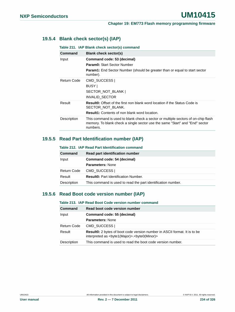
NXP Semiconductors UM10415Chapter 19: EM773 Flash memory programming firmware
19.5.4 Blank check sector(s) (IAP)
19.5.5 Read Part Identification number (IAP)
19.5.6 Read Boot code version number (IAP)
Table 211. IAP Blank check sector(s) command
Command Blank check sector(s)
Input Command code: 53 (decimal)
Param0: Start Sector Number
Param1: End Sector Number (should be greater than or equal to start sector number).
Return Code CMD_SUCCESS |
BUSY |
SECTOR_NOT_BLANK |
INVALID_SECTOR
Result Result0: Offset of the first non blank word location if the Status Code is SECTOR_NOT_BLANK.
Result1: Contents of non blank word location.
Description This command is used to blank check a sector or multiple sectors of on-chip flash memory. To blank check a single sector use the same "Start" and "End" sector numbers.
Table 212. IAP Read Part Identification command
Command Read part identification number
Input Command code: 54 (decimal)
Parameters: None
Return Code CMD_SUCCESS |
Result Result0: Part Identification Number.
Description This command is used to read the part identification number.
Table 213. IAP Read Boot Code version number command
Command Read boot code version number
Input Command code: 55 (decimal)
Parameters: None
Return Code CMD_SUCCESS |
Result Result0: 2 bytes of boot code version number in ASCII format. It is to be interpreted as <byte1(Major)>.<byte0(Minor)>
Description This command is used to read the boot code version number.
UM10415 All information provided in this document is subject to legal disclaimers. © NXP B.V. 2011. All rights reserved.
User manual Rev. 2 — 7 December 2011 234 of 326

NXP Semiconductors UM10415Chapter 19: EM773 Flash memory programming firmware
19.5.7 Compare <address1> <address2> <no of bytes> (IAP)
19.5.8 Reinvoke ISP (IAP)
19.5.9 ReadUID (IAP)
Table 214. IAP Compare command
Command Compare
Input Command code: 56 (decimal)
Param0(DST): Starting flash or RAM address of data bytes to be compared. This address should be a word boundary.
Param1(SRC): Starting flash or RAM address of data bytes to be compared. This address should be a word boundary.
Param2: Number of bytes to be compared; should be a multiple of 4.
Return Code CMD_SUCCESS |
COMPARE_ERROR |
COUNT_ERROR (Byte count is not a multiple of 4) |
ADDR_ERROR |
ADDR_NOT_MAPPED
Result Result0: Offset of the first mismatch if the Status Code is COMPARE_ERROR.
Description This command is used to compare the memory contents at two locations.
The result may not be correct when the source or destination includes any of the first 512 bytes starting from address zero. The first 512 bytes can be re-mapped to RAM.
Table 215. IAP Reinvoke ISP
Command Compare
Input Command code: 57 (decimal)
Return Code None
Result None.
Description This command is used to invoke the bootloader in ISP mode. It maps boot vectors, sets PCLK = CCLK, configures UART pins RXD and TXD, resets counter/timer CT32B1 and resets the U0FDR (see Table 105). This command may be used when a valid user program is present in the internal flash memory and the PIO0_1 pin is not accessible to force the ISP mode.
Table 216. IAP ReadUID command
Command Compare
Input Command code: 58 (decimal)
Return Code CMD_SUCCESS
Result Result0: The first 32-bit word (at the lowest address).Result1: The second 32-bit word.Result2: The third 32-bit word.Result3: The fourth 32-bit word.
Description This command is used to read the unique ID.
UM10415 All information provided in this document is subject to legal disclaimers. © NXP B.V. 2011. All rights reserved.
User manual Rev. 2 — 7 December 2011 235 of 326
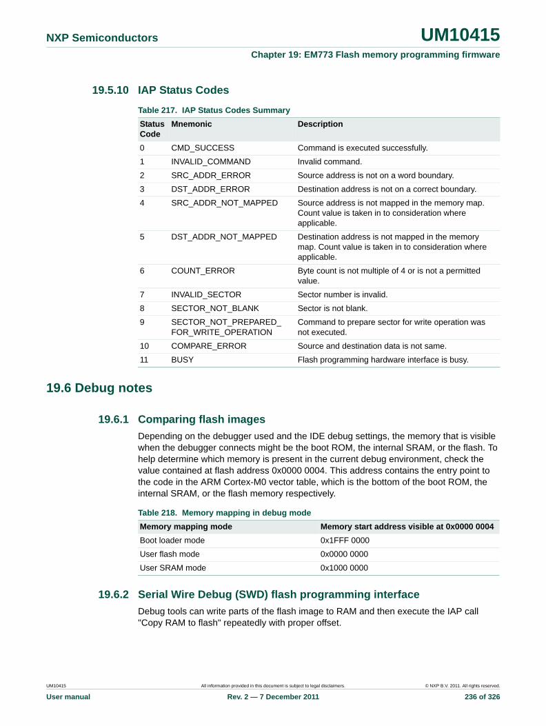
NXP Semiconductors UM10415Chapter 19: EM773 Flash memory programming firmware
19.5.10 IAP Status Codes
19.6 Debug notes
19.6.1 Comparing flash images
Depending on the debugger used and the IDE debug settings, the memory that is visible when the debugger connects might be the boot ROM, the internal SRAM, or the flash. To help determine which memory is present in the current debug environment, check the value contained at flash address 0x0000 0004. This address contains the entry point to the code in the ARM Cortex-M0 vector table, which is the bottom of the boot ROM, the internal SRAM, or the flash memory respectively.
19.6.2 Serial Wire Debug (SWD) flash programming interface
Debug tools can write parts of the flash image to RAM and then execute the IAP call "Copy RAM to flash" repeatedly with proper offset.
Table 217. IAP Status Codes Summary
Status Code
Mnemonic Description
0 CMD_SUCCESS Command is executed successfully.
1 INVALID_COMMAND Invalid command.
2 SRC_ADDR_ERROR Source address is not on a word boundary.
3 DST_ADDR_ERROR Destination address is not on a correct boundary.
4 SRC_ADDR_NOT_MAPPED Source address is not mapped in the memory map. Count value is taken in to consideration where applicable.
5 DST_ADDR_NOT_MAPPED Destination address is not mapped in the memory map. Count value is taken in to consideration where applicable.
6 COUNT_ERROR Byte count is not multiple of 4 or is not a permitted value.
7 INVALID_SECTOR Sector number is invalid.
8 SECTOR_NOT_BLANK Sector is not blank.
9 SECTOR_NOT_PREPARED_FOR_WRITE_OPERATION
Command to prepare sector for write operation was not executed.
10 COMPARE_ERROR Source and destination data is not same.
11 BUSY Flash programming hardware interface is busy.
Table 218. Memory mapping in debug mode
Memory mapping mode Memory start address visible at 0x0000 0004
Boot loader mode 0x1FFF 0000
User flash mode 0x0000 0000
User SRAM mode 0x1000 0000
UM10415 All information provided in this document is subject to legal disclaimers. © NXP B.V. 2011. All rights reserved.
User manual Rev. 2 — 7 December 2011 236 of 326

NXP Semiconductors UM10415Chapter 19: EM773 Flash memory programming firmware
19.7 Flash memory access
Depending on the system clock frequency, access to the flash memory can be configured with various access times by writing to the FLASHCFG register at address 0x4003 C010.
Remark: Improper setting of this register may result in incorrect operation of the EM773 flash memory.
Table 219. Flash configuration register (FLASHCFG, address 0x4003 C010) bit description
Bit Symbol Value Description Reset value
1:0 FLASHTIM Flash memory access time. FLASHTIM +1 is equal to the number of system clocks used for flash access.
10
00 1 system clock flash access time (for system clock frequencies of up to 20 MHz).
01 2 system clocks flash access time (for system clock frequencies of up to 40 MHz).
10 3 system clocks flash access time (for system clock frequencies of up to 48 MHz).
11 Reserved.
31:2 - - Reserved. User software must not change the value of these bits. Bits 31:2 must be written back exactly as read.
<tbd>
UM10415 All information provided in this document is subject to legal disclaimers. © NXP B.V. 2011. All rights reserved.
User manual Rev. 2 — 7 December 2011 237 of 326

20.1 How to read this chapter
The debug functionality is identical for all EM773 parts.
20.2 Features
• Supports ARM Serial Wire Debug mode.
• Direct debug access to all memories, registers, and peripherals.
• No target resources are required for the debugging session.
• Four breakpoints. Four instruction breakpoints that can also be used to remap instruction addresses for code patches. Two data comparators that can be used to remap addresses for patches to literal values.
• Two data watchpoints that can also be used as triggers.
20.3 Introduction
Debug functions are integrated into the ARM Cortex-M0. Serial wire debug functions are supported. The ARM Cortex-M0 is configured to support up to four breakpoints and two watchpoints.
20.4 Description
Debugging with the EM773 uses the Serial Wire Debug mode.
20.5 Pin description
The tables below indicate the various pin functions related to debug. Some of these functions share pins with other functions which therefore may not be used at the same time.
UM10415Chapter 20: EM773 Serial Wire Debug (SWD)Rev. 2 — 7 December 2011 User manual
Table 220. Serial Wire Debug pin description
Pin Name Type Description
SWCLK Input Serial Wire Clock. This pin is the clock for debug logic when in the Serial Wire Debug mode (SWDCLK).
SWDIO Input / Output
Serial wire debug data input/output. The SWDIO pin is used by an external debug tool to communicate with and control the EM773.
UM10415 All information provided in this document is subject to legal disclaimers. © NXP B.V. 2011. All rights reserved.
User manual Rev. 2 — 7 December 2011 238 of 326

NXP Semiconductors UM10415Chapter 20: EM773 Serial Wire Debug (SWD)
20.6 Debug Notes
Important: The user should be aware of certain limitations during debugging. The most important is that, due to limitations of the ARM Cortex-M0 integration, the EM773 cannot wake up in the usual manner from Deep-sleep mode. It is recommended not to use this mode during debug.
Another issue is that debug mode changes the way in which reduced power modes work internal to the ARM Cortex-M0 CPU, and this ripples through the entire system. These differences mean that power measurements should not be made while debugging, the results will be higher than during normal operation in an application.
During a debugging session, the System Tick Timer is automatically stopped whenever the CPU is stopped. Other peripherals are not affected.
UM10415 All information provided in this document is subject to legal disclaimers. © NXP B.V. 2011. All rights reserved.
User manual Rev. 2 — 7 December 2011 239 of 326

21.1 Introduction
The following material is using the ARM Cortex-M0 User Guide. Minor changes have been made regarding the specific implementation of the Cortex-M0 for the EM773.
The ARM Cortex-M0 documentation is also available in Ref. 1 and Ref. 2.
21.2 About the Cortex-M0 processor and core peripherals
The Cortex-M0 processor is an entry-level 32-bit ARM Cortex processor designed for a broad range of embedded applications. It offers significant benefits to developers, including:
• a simple architecture that is easy to learn and program
• ultra-low power, energy efficient operation
• excellent code density
• deterministic, high-performance interrupt handling
• upward compatibility with Cortex-M processor family.
The Cortex-M0 processor is built on a highly area and power optimized 32-bit processor core, with a 3-stage pipeline von Neumann architecture. The processor delivers exceptional energy efficiency through a small but powerful instruction set and extensively optimized design, providing high-end processing hardware including a single-cycle multiplier.
The Cortex-M0 processor implements the ARMv6-M architecture, which is based on the 16-bit Thumb instruction set and includes Thumb-2 technology. This provides the exceptional performance expected of a modern 32-bit architecture, with a higher code density than other 8-bit and 16-bit microcontrollers.
UM10415Chapter 21: Appendix EM773 ARM Cortex-M0 referenceRev. 2 — 7 December 2011 User manual
Fig 59. Cortex-M0 implementation
����������� �����
����������� �����
���
����������
��������� ����������������
����������������
����������
������� ����!����
���!�
�"��#���������$� ������%���� &������'��������������
�����
�������������$� �
����*����������
+�� .����������
�������� ���������
UM10415 All information provided in this document is subject to legal disclaimers. © NXP B.V. 2011. All rights reserved.
User manual Rev. 2 — 7 December 2011 240 of 326

NXP Semiconductors UM10415Chapter 21: Appendix EM773 ARM Cortex-M0 reference
The Cortex-M0 processor closely integrates a configurable Nested Vectored Interrupt Controller (NVIC), to deliver industry-leading interrupt performance. The NVIC:
• includes a non-maskable interrupt (NMI). The NMI is not implemented on the EM773.
• provides zero jitter interrupt option
• provides four interrupt priority levels.
The tight integration of the processor core and NVIC provides fast execution of interrupt service routines (ISRs), dramatically reducing the interrupt latency. This is achieved through the hardware stacking of registers, and the ability to abandon and restart load-multiple and store-multiple operations. Interrupt handlers do not require any assembler wrapper code, removing any code overhead from the ISRs. Tail-chaining optimization also significantly reduces the overhead when switching from one ISR to another.
To optimize low-power designs, the NVIC integrates with the sleep modes, that include a Deep-sleep function that enables the entire device to be rapidly powered down.
21.2.1 System-level interface
The Cortex-M0 processor provides a single system-level interface using AMBA technology to provide high speed, low latency memory accesses.
21.2.2 Integrated configurable debug
The Cortex-M0 processor implements a complete hardware debug solution, with extensive hardware breakpoint and watchpoint options. This provides high system visibility of the processor, memory and peripherals through a 2-pin Serial Wire Debug (SWD) port that is ideal for microcontrollers and other small package devices.
21.2.3 Cortex-M0 processor features summary
• high code density with 32-bit performance
• tools and binary upwards compatible with Cortex-M processor family
• integrated ultra low-power sleep modes
• efficient code execution permits slower processor clock or increases sleep mode time
• single-cycle 32-bit hardware multiplier
• zero jitter interrupt handling
• extensive debug capabilities.
21.2.4 Cortex-M0 core peripherals
These are:
NVIC — The NVIC is an embedded interrupt controller that supports low latency interrupt processing.
UM10415 All information provided in this document is subject to legal disclaimers. © NXP B.V. 2011. All rights reserved.
User manual Rev. 2 — 7 December 2011 241 of 326
NXP Semiconductors UM10415Chapter 21: Appendix EM773 ARM Cortex-M0 reference
System Control Block — The System Control Block (SCB) is the programmers model interface to the processor. It provides system implementation information and system control, including configuration, control, and reporting of system exceptions.
System timer — The system timer, SysTick, is a 24-bit count-down timer. Use this as a Real Time Operating System (RTOS) tick timer or as a simple counter.
21.3 Processor
21.3.1 Programmers model
This section describes the Cortex-M0 programmers model. In addition to the individual core register descriptions, it contains information about the processor modes and stacks.
21.3.1.1 Processor modes
The processor modes are:
Thread mode — Used to execute application software. The processor enters Thread mode when it comes out of reset.
Handler mode — Used to handle exceptions. The processor returns to Thread mode when it has finished all exception processing.
21.3.1.2 Stacks
The processor uses a full descending stack. This means the stack pointer indicates the last stacked item on the stack memory. When the processor pushes a new item onto the stack, it decrements the stack pointer and then writes the item to the new memory location. The processor implements two stacks, the main stack and the process stack, with independent copies of the stack pointer, see Section 21.3.1.3.2.
In Thread mode, the CONTROL register controls whether the processor uses the main stack or the process stack, see Section 21–21.3.1.3.7. In Handler mode, the processor always uses the main stack. The options for processor operations are:
21.3.1.3 Core registers
The processor core registers are:
Table 221. Summary of processor mode and stack use options
Processormode
Used toexecute
Stack used
Thread Applications Main stack or process stack
See Section 21–21.3.1.3.7
Handler Exception handlers
Main stack
UM10415 All information provided in this document is subject to legal disclaimers. © NXP B.V. 2011. All rights reserved.
User manual Rev. 2 — 7 December 2011 242 of 326

NXP Semiconductors UM10415Chapter 21: Appendix EM773 ARM Cortex-M0 reference
[1] Describes access type during program execution in thread mode and Handler mode. Debug access can differ.
[2] Bit[24] is the T-bit and is loaded from bit[0] of the reset vector.
21.3.1.3.1 General-purpose registers
R0-R12 are 32-bit general-purpose registers for data operations.
21.3.1.3.2 Stack Pointer
The Stack Pointer (SP) is register R13. In Thread mode, bit[1] of the CONTROL register indicates the stack pointer to use:
• 0 = Main Stack Pointer (MSP). This is the reset value.
• 1 = Process Stack Pointer (PSP).
Fig 60. Processor core register set
Table 222. Core register set summary
Name Type[1] Reset value Description
R0-R12 RW Unknown Section 21–21.3.1.3.1
MSP RW See description Section 21–21.3.1.3.2
PSP RW Unknown Section 21–21.3.1.3.2
LR RW Unknown Section 21–21.3.1.3.3
PC RW See description Section 21–21.3.1.3.4
PSR RW Unknown[2] Table 21–223
APSR RW Unknown Table 21–224
IPSR RO 0x00000000 Table 225
EPSR RO Unknown[2] Table 21–226
PRIMASK RW 0x00000000 Table 21–227
CONTROL RW 0x00000000 Table 21–228
����������� �
�����������������������
������
����
����
��
���������
����
����� ���� ��
��!�� ���� ��
"�����
#$%�#�
���
���&�� ���� ����'&������ �
( � ��)�*�*�� �� ���� ��
��������������� ���� �
�����)�� ���� ��* '��)�� ���� ����+",�- +�� ��*�����&�� ���� �
UM10415 All information provided in this document is subject to legal disclaimers. © NXP B.V. 2011. All rights reserved.
User manual Rev. 2 — 7 December 2011 243 of 326

NXP Semiconductors UM10415Chapter 21: Appendix EM773 ARM Cortex-M0 reference
On reset, the processor loads the MSP with the value from address 0x00000000.
21.3.1.3.3 Link Register
The Link Register (LR) is register R14. It stores the return information for subroutines, function calls, and exceptions. On reset, the LR value is Unknown.
21.3.1.3.4 Program Counter
The Program Counter (PC) is register R15. It contains the current program address. On reset, the processor loads the PC with the value of the reset vector, which is at address 0x00000004. Bit[0] of the value is loaded into the EPSR T-bit at reset and must be 1.
21.3.1.3.5 Program Status Register
The Program Status Register (PSR) combines:
• Application Program Status Register (APSR)
• Interrupt Program Status Register (IPSR)
• Execution Program Status Register (EPSR).
These registers are mutually exclusive bitfields in the 32-bit PSR. The PSR bit assignments are:
Access these registers individually or as a combination of any two or all three registers, using the register name as an argument to the MSR or MRS instructions. For example:
• read all of the registers using PSR with the MRS instruction
• write to the APSR using APSR with the MSR instruction.
The PSR combinations and attributes are:
[1] The processor ignores writes to the IPSR bits.
[2] Reads of the EPSR bits return zero, and the processor ignores writes to the these bits
Fig 61. APSR, IPSR, EPSR register bit assignments
Table 223. PSR register combinations
Register Type Combination
PSR RW[1][2] APSR, EPSR, and IPSR
IEPSR RO EPSR and IPSR
IAPSR RW[1] APSR and IPSR
EAPSR RW[2] APSR and EPSR
�� �� ��
� � �. / 01' *�������2 �
�� �� �� �� ��
$ 3 4
�
� � �. /,���
+���
0��� � � �. / � � �. /%
��
UM10415 All information provided in this document is subject to legal disclaimers. © NXP B.V. 2011. All rights reserved.
User manual Rev. 2 — 7 December 2011 244 of 326

NXP Semiconductors UM10415Chapter 21: Appendix EM773 ARM Cortex-M0 reference
See the instruction descriptions Section 21–21.4.7.6 and Section 21–21.4.7.7 for more information about how to access the program status registers.
Application Program Status Register: The APSR contains the current state of the condition flags, from previous instruction executions. See the register summary in Table 21–222 for its attributes. The bit assignments are:
See Section 21.4.4.1.4 for more information about the APSR negative, zero, carry or borrow, and overflow flags.
Interrupt Program Status Register: The IPSR contains the exception number of the current Interrupt Service Routine (ISR). See the register summary in Table 21–222 for its attributes. The bit assignments are:
Execution Program Status Register: The EPSR contains the Thumb state bit.
See the register summary in Table 21–222 for the EPSR attributes. The bit assignments are:
Table 224. APSR bit assignments
Bits Name Function
[31] N Negative flag
[30] Z Zero flag
[29] C Carry or borrow flag
[28] V Overflow flag
[27:0] - Reserved
Table 225. IPSR bit assignments
Bits Name Function
[31:6] - Reserved
[5:0] Exception number This is the number of the current exception:
0 = Thread mode
1 = Reserved
2 = NMI
3 = HardFault
4-10 = Reserved
11 = SVCall
12, 13 = Reserved
14 = PendSV
15 = SysTick
16 = IRQ0
.
.
.
47 = IRQ31
48-63 = Reserved.
see Section 21–21.3.3.2 for more information.
UM10415 All information provided in this document is subject to legal disclaimers. © NXP B.V. 2011. All rights reserved.
User manual Rev. 2 — 7 December 2011 245 of 326

NXP Semiconductors UM10415Chapter 21: Appendix EM773 ARM Cortex-M0 reference
Attempts by application software to read the EPSR directly using the MRS instruction always return zero. Attempts to write the EPSR using the MSR instruction are ignored. Fault handlers can examine the EPSR value in the stacked PSR to determine the cause of the fault. See Section 21–21.3.3.6. The following can clear the T bit to 0:
• instructions BLX, BX and POP{PC}
• restoration from the stacked xPSR value on an exception return
• bit[0] of the vector value on an exception entry.
Attempting to execute instructions when the T bit is 0 results in a HardFault or lockup. See Section 21–21.3.4.1 for more information.
Interruptible-restartable instructions: The interruptible-restartable instructions are LDM and STM. When an interrupt occurs during the execution of one of these instructions, the processor abandons execution of the instruction.
After servicing the interrupt, the processor restarts execution of the instruction from the beginning.
21.3.1.3.6 Exception mask register
The exception mask register disables the handling of exceptions by the processor. Disable exceptions where they might impact on timing critical tasks or code sequences requiring atomicity.
To disable or re-enable exceptions, use the MSR and MRS instructions, or the CPS instruction, to change the value of PRIMASK. See Section 21–21.4.7.6, Section 21–21.4.7.7, and Section 21–21.4.7.2 for more information.
Priority Mask Register: The PRIMASK register prevents activation of all exceptions with configurable priority. See the register summary in Table 21–222 for its attributes. The bit assignments are:
21.3.1.3.7 CONTROL register
The CONTROL register controls the stack used when the processor is in Thread mode. See the register summary in Table 21–222 for its attributes. The bit assignments are:
Table 226. EPSR bit assignments
Bits Name Function
[31:25] - Reserved
[24] T Thumb state bit
[23:0] - Reserved
Table 227. PRIMASK register bit assignments
Bits Name Function
[31:1] - Reserved
[0] PRIMASK 0 = no effect
1 = prevents the activation of all exceptions with configurable priority.
UM10415 All information provided in this document is subject to legal disclaimers. © NXP B.V. 2011. All rights reserved.
User manual Rev. 2 — 7 December 2011 246 of 326
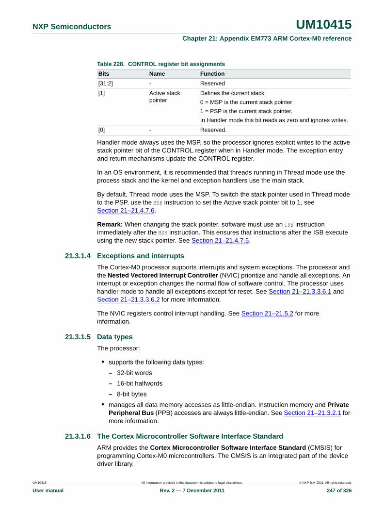
NXP Semiconductors UM10415Chapter 21: Appendix EM773 ARM Cortex-M0 reference
Handler mode always uses the MSP, so the processor ignores explicit writes to the active stack pointer bit of the CONTROL register when in Handler mode. The exception entry and return mechanisms update the CONTROL register.
In an OS environment, it is recommended that threads running in Thread mode use the process stack and the kernel and exception handlers use the main stack.
By default, Thread mode uses the MSP. To switch the stack pointer used in Thread mode to the PSP, use the MSR instruction to set the Active stack pointer bit to 1, see Section 21–21.4.7.6.
Remark: When changing the stack pointer, software must use an ISB instruction immediately after the MSR instruction. This ensures that instructions after the ISB execute using the new stack pointer. See Section 21–21.4.7.5.
21.3.1.4 Exceptions and interrupts
The Cortex-M0 processor supports interrupts and system exceptions. The processor and the Nested Vectored Interrupt Controller (NVIC) prioritize and handle all exceptions. An interrupt or exception changes the normal flow of software control. The processor uses handler mode to handle all exceptions except for reset. See Section 21–21.3.3.6.1 and Section 21–21.3.3.6.2 for more information.
The NVIC registers control interrupt handling. See Section 21–21.5.2 for more information.
21.3.1.5 Data types
The processor:
• supports the following data types:
– 32-bit words
– 16-bit halfwords
– 8-bit bytes
• manages all data memory accesses as little-endian. Instruction memory and Private Peripheral Bus (PPB) accesses are always little-endian. See Section 21–21.3.2.1 for more information.
21.3.1.6 The Cortex Microcontroller Software Interface Standard
ARM provides the Cortex Microcontroller Software Interface Standard (CMSIS) for programming Cortex-M0 microcontrollers. The CMSIS is an integrated part of the device driver library.
Table 228. CONTROL register bit assignments
Bits Name Function
[31:2] - Reserved
[1] Active stack pointer
Defines the current stack:
0 = MSP is the current stack pointer
1 = PSP is the current stack pointer.
In Handler mode this bit reads as zero and ignores writes.
[0] - Reserved.
UM10415 All information provided in this document is subject to legal disclaimers. © NXP B.V. 2011. All rights reserved.
User manual Rev. 2 — 7 December 2011 247 of 326

NXP Semiconductors UM10415Chapter 21: Appendix EM773 ARM Cortex-M0 reference
For a Cortex-M0 microcontroller system, CMSIS defines:
• a common way to:
– access peripheral registers
– define exception vectors
• the names of:
– the registers of the core peripherals
– the core exception vectors
• a device-independent interface for RTOS kernels.
The CMSIS includes address definitions and data structures for the core peripherals in the Cortex-M0 processor. It also includes optional interfaces for middleware components comprising a TCP/IP stack and a Flash file system.
The CMSIS simplifies software development by enabling the reuse of template code, and the combination of CMSIS-compliant software components from various middleware vendors. Software vendors can expand the CMSIS to include their peripheral definitions and access functions for those peripherals.
This document includes the register names defined by the CMSIS, and gives short descriptions of the CMSIS functions that address the processor core and the core peripherals.
Remark: This document uses the register short names defined by the CMSIS. In a few cases these differ from the architectural short names that might be used in other documents.
The following sections give more information about the CMSIS:
• Section 21.3.5.3 “Power management programming hints”
• Section 21.4.2 “Intrinsic functions”
• Section 21.5.2.1 “Accessing the Cortex-M0 NVIC registers using CMSIS”
• Section 21.5.2.8.1 “NVIC programming hints”.
21.3.2 Memory model
This section describes the processor memory map and the behavior of memory accesses. The processor has a fixed memory map that provides up to 4GB of addressable memory. The memory map is:
UM10415 All information provided in this document is subject to legal disclaimers. © NXP B.V. 2011. All rights reserved.
User manual Rev. 2 — 7 December 2011 248 of 326

NXP Semiconductors UM10415Chapter 21: Appendix EM773 ARM Cortex-M0 reference
The processor reserves regions of the Private peripheral bus (PPB) address range for core peripheral registers, see Section 21–21.2.
21.3.2.1 Memory regions, types and attributes
The memory map is split into regions. Each region has a defined memory type, and some regions have additional memory attributes. The memory type and attributes determine the behavior of accesses to the region.
The memory types are:
Normal — The processor can re-order transactions for efficiency, or perform speculative reads.
Device — The processor preserves transaction order relative to other transactions to Device or Strongly-ordered memory.
See Figure 2 for the EM773 specific implementation of the memory map.
Fig 62. Generic ARM Cortex-M0 memory map
01� ���)�/ .�'
01� ���)��,"
� ��*! ��)
��,"
�/
����������
���.�� �* ��*! ��)�2���������������������
��������������������
������������������
��������������������
������������ �������
����������
�5�(6
�5�(6
�5�(6
�5�(6
�5�(6
���������������������"6
���"67 .�'
UM10415 All information provided in this document is subject to legal disclaimers. © NXP B.V. 2011. All rights reserved.
User manual Rev. 2 — 7 December 2011 249 of 326
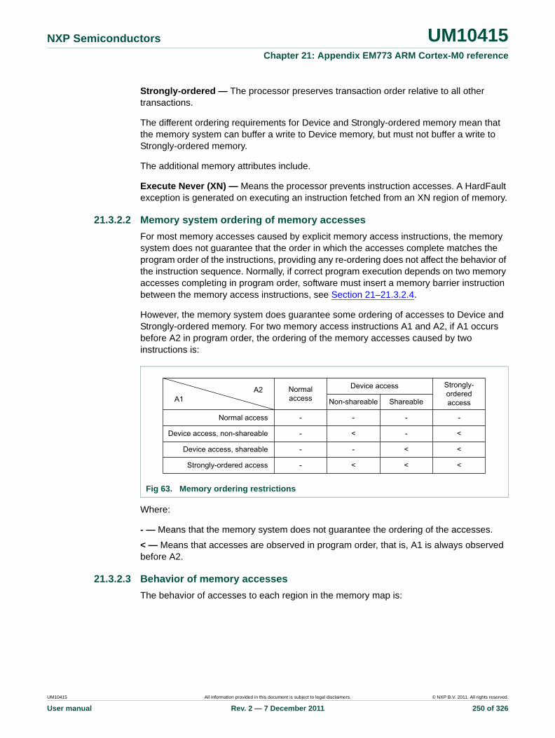
NXP Semiconductors UM10415Chapter 21: Appendix EM773 ARM Cortex-M0 reference
Strongly-ordered — The processor preserves transaction order relative to all other transactions.
The different ordering requirements for Device and Strongly-ordered memory mean that the memory system can buffer a write to Device memory, but must not buffer a write to Strongly-ordered memory.
The additional memory attributes include.
Execute Never (XN) — Means the processor prevents instruction accesses. A HardFault exception is generated on executing an instruction fetched from an XN region of memory.
21.3.2.2 Memory system ordering of memory accesses
For most memory accesses caused by explicit memory access instructions, the memory system does not guarantee that the order in which the accesses complete matches the program order of the instructions, providing any re-ordering does not affect the behavior of the instruction sequence. Normally, if correct program execution depends on two memory accesses completing in program order, software must insert a memory barrier instruction between the memory access instructions, see Section 21–21.3.2.4.
However, the memory system does guarantee some ordering of accesses to Device and Strongly-ordered memory. For two memory access instructions A1 and A2, if A1 occurs before A2 in program order, the ordering of the memory accesses caused by two instructions is:
Where:
- — Means that the memory system does not guarantee the ordering of the accesses.
< — Means that accesses are observed in program order, that is, A1 is always observed before A2.
21.3.2.3 Behavior of memory accesses
The behavior of accesses to each region in the memory map is:
Fig 63. Memory ordering restrictions
$����)��'' ��
7 .�' ��'' ��8����9�!�� �2)
7 .�' ��'' ��8��!�� �2)
������):9��/ � /��'' ��
$����)�'' �� $��9�!�� �2) �!�� �2)
������):9��/ � /�'' ��
7 .�' ��'' ��
,�,�
9
9
9
9
9
;
9
;
9
9
;
;
9
;
;
;
UM10415 All information provided in this document is subject to legal disclaimers. © NXP B.V. 2011. All rights reserved.
User manual Rev. 2 — 7 December 2011 250 of 326

NXP Semiconductors UM10415Chapter 21: Appendix EM773 ARM Cortex-M0 reference
[1] See Section 21–21.3.2.1 for more information.
The Code, SRAM, and external RAM regions can hold programs.
21.3.2.4 Software ordering of memory accesses
The order of instructions in the program flow does not always guarantee the order of the corresponding memory transactions. This is because:
• the processor can reorder some memory accesses to improve efficiency, providing this does not affect the behavior of the instruction sequence
• memory or devices in the memory map might have different wait states
• some memory accesses are buffered or speculative.
Section 21–21.3.2.2 describes the cases where the memory system guarantees the order of memory accesses. Otherwise, if the order of memory accesses is critical, software must include memory barrier instructions to force that ordering. The processor provides the following memory barrier instructions:
DMB — The Data Memory Barrier (DMB) instruction ensures that outstanding memory transactions complete before subsequent memory transactions. See Section 21–21.4.7.3.
DSB — The Data Synchronization Barrier (DSB) instruction ensures that outstanding memory transactions complete before subsequent instructions execute. See Section 21–21.4.7.4.
ISB — The Instruction Synchronization Barrier (ISB) ensures that the effect of all completed memory transactions is recognizable by subsequent instructions. See Section 21–21.4.7.5.
The following are examples of using memory barrier instructions:
Table 229. Memory access behavior
Addressrange
Memoryregion
Memorytype[1]
XN[1] Description
0x00000000- 0x1FFFFFFF
Code Normal - Executable region for program code. You can also put data here.
0x20000000- 0x3FFFFFFF
SRAM Normal - Executable region for data. You can also put code here.
0x40000000- 0x5FFFFFFF
Peripheral Device XN External device memory.
0x60000000- 0x9FFFFFFF
ExternalRAM
Normal - Executable region for data.
0xA0000000- 0xDFFFFFFF
Externaldevice
Device XN External device memory.
0xE0000000- 0xE00FFFFF
Private Peripheral Bus
Strongly-ordered XN This region includes the NVIC, System timer, and System Control Block. Only word accesses can be used in this region.
0xE0100000- 0xFFFFFFFF
Device Device XN Vendor specific.
UM10415 All information provided in this document is subject to legal disclaimers. © NXP B.V. 2011. All rights reserved.
User manual Rev. 2 — 7 December 2011 251 of 326

NXP Semiconductors UM10415Chapter 21: Appendix EM773 ARM Cortex-M0 reference
Vector table — If the program changes an entry in the vector table, and then enables the corresponding exception, use a DMB instruction between the operations. This ensures that if the exception is taken immediately after being enabled the processor uses the new exception vector.
Self-modifying code — If a program contains self-modifying code, use an ISB instruction immediately after the code modification in the program. This ensures subsequent instruction execution uses the updated program.
Memory map switching — If the system contains a memory map switching mechanism, use a DSB instruction after switching the memory map. This ensures subsequent instruction execution uses the updated memory map.
Memory accesses to Strongly-ordered memory, such as the System Control Block, do not require the use of DMB instructions.
The processor preserves transaction order relative to all other transactions.
21.3.2.5 Memory endianness
The processor views memory as a linear collection of bytes numbered in ascending order from zero. For example, bytes 0-3 hold the first stored word, and bytes 4-7 hold the second stored word. Section 21–21.3.2.5.1 describes how words of data are stored in memory.
21.3.2.5.1 Little-endian format
In little-endian format, the processor stores the least significant byte (lsbyte) of a word at the lowest-numbered byte, and the most significant byte (msbyte) at the highest-numbered byte. For example:
21.3.3 Exception model
This section describes the exception model.
21.3.3.1 Exception states
Each exception is in one of the following states:
Inactive — The exception is not active and not pending.
Pending — The exception is waiting to be serviced by the processor.
Fig 64. Little-endian format
� ���� �
,<�
)�2:�
��2:�
,<�
,<�
��
6�6�6� 6��� ���� ���� � � �
6�
6�
6�
6�
" ���:
,,//� ��
UM10415 All information provided in this document is subject to legal disclaimers. © NXP B.V. 2011. All rights reserved.
User manual Rev. 2 — 7 December 2011 252 of 326

NXP Semiconductors UM10415Chapter 21: Appendix EM773 ARM Cortex-M0 reference
An interrupt request from a peripheral or from software can change the state of the corresponding interrupt to pending.
Active — An exception that is being serviced by the processor but has not completed.
An exception handler can interrupt the execution of another exception handler. In this case both exceptions are in the active state.
Active and pending — The exception is being serviced by the processor and there is a pending exception from the same source.
21.3.3.2 Exception types
The exception types are:
Remark: The NMI is not implemented on the EM773.
Reset — Reset is invoked on power up or a warm reset. The exception model treats reset as a special form of exception. When reset is asserted, the operation of the processor stops, potentially at any point in an instruction. When reset is deasserted, execution restarts from the address provided by the reset entry in the vector table. Execution restarts in Thread mode.
NMI — A NonMaskable Interrupt (NMI) can be signalled by a peripheral or triggered by software. This is the highest priority exception other than reset. It is permanently enabled and has a fixed priority of 2. NMIs cannot be:
• masked or prevented from activation by any other exception
• preempted by any exception other than Reset.
HardFault — A HardFault is an exception that occurs because of an error during normal or exception processing. HardFaults have a fixed priority of -1, meaning they have higher priority than any exception with configurable priority.
SVCall — A supervisor call (SVC) is an exception that is triggered by the SVC instruction. In an OS environment, applications can use SVC instructions to access OS kernel functions and device drivers.
PendSV — PendSV is an interrupt-driven request for system-level service. In an OS environment, use PendSV for context switching when no other exception is active.
SysTick — A SysTick exception is an exception the system timer generates when it reaches zero. Software can also generate a SysTick exception. In an OS environment, the processor can use this exception as system tick.
Interrupt (IRQ) — An interrupt, or IRQ, is an exception signalled by a peripheral, or generated by a software request. All interrupts are asynchronous to instruction execution. In the system, peripherals use interrupts to communicate with the processor.
Table 230. Properties of different exception types
Exceptionnumber[1]
IRQnumber[1]
Exceptiontype
Priority Vector address[2]
1 - Reset -3, the highest 0x00000004
2 -14 NMI -2 0x00000008
3 -13 HardFault -1 0x0000000C
4-10 - Reserved - -
11 -5 SVCall Configurable[3] 0x0000002C
UM10415 All information provided in this document is subject to legal disclaimers. © NXP B.V. 2011. All rights reserved.
User manual Rev. 2 — 7 December 2011 253 of 326

NXP Semiconductors UM10415Chapter 21: Appendix EM773 ARM Cortex-M0 reference
[1] To simplify the software layer, the CMSIS only uses IRQ numbers and therefore uses negative values for exceptions other than interrupts. The IPSR returns the Exception number, see Table 21–225.
[2] See Section 21.3.3.4 for more information.
[3] See Section 21–21.5.2.6.
[4] Increasing in steps of 4.
For an asynchronous exception, other than reset, the processor can execute additional instructions between when the exception is triggered and when the processor enters the exception handler.
Privileged software can disable the exceptions that Table 21–230 shows as having configurable priority, see Section 21–21.5.2.3.
For more information about HardFaults, see Section 21–21.3.4.
21.3.3.3 Exception handlers
The processor handles exceptions using:
Interrupt Service Routines (ISRs) — Interrupts IRQ0 to IRQ31 are the exceptions handled by ISRs.
Fault handler — HardFault is the only exception handled by the fault handler.
System handlers — NMI, PendSV, SVCall SysTick, and HardFault are all system exceptions handled by system handlers.
21.3.3.4 Vector table
The vector table contains the reset value of the stack pointer, and the start addresses, also called exception vectors, for all exception handlers. Figure 21–65 shows the order of the exception vectors in the vector table. The least-significant bit of each vector must be 1, indicating that the exception handler is written in Thumb code.
12-13 - Reserved - -
14 -2 PendSV Configurable[3] 0x00000038
15 -1 SysTick Configurable[3] 0x0000003C
16 and above 0 and above Interrupt (IRQ) Configurable[3] 0x00000040 and above[4]
Table 230. Properties of different exception types …continued
Exceptionnumber[1]
IRQnumber[1]
Exceptiontype
Priority Vector address[2]
UM10415 All information provided in this document is subject to legal disclaimers. © NXP B.V. 2011. All rights reserved.
User manual Rev. 2 — 7 December 2011 254 of 326

NXP Semiconductors UM10415Chapter 21: Appendix EM773 ARM Cortex-M0 reference
The vector table is fixed at address 0x00000000.
21.3.3.5 Exception priorities
As Table 21–230 shows, all exceptions have an associated priority, with:
• a lower priority value indicating a higher priority
• configurable priorities for all exceptions except Reset, HardFault, and NMI.
If software does not configure any priorities, then all exceptions with a configurable priority have a priority of 0. For information about configuring exception priorities see
• Section 21–21.5.3.7
• Section 21–21.5.2.6.
Remark: Configurable priority values are in the range 0-3. The Reset, HardFault, and NMI exceptions, with fixed negative priority values, always have higher priority than any other exception.
Fig 65. Vector table
+�����)����.�)
� � �
��/=�)�
$"+
�1��
�1��
�1��
�1�
�1��
� � �. /
�4�))
� �/�4
�:�%�'&
+�>�
� � �. /
�1�
�1��
�1�
�1��
#??� �01' *�������2 �
�
�
�
�
�
��
��
��
��
��
��
��
�
��
�
4 '���
555
�
�
+�>�
+�>�
�1��
+�>��
���1��
��
555
555
�16
+�>���2 �
9��
9��
9�
9�
9�
�
�
�
��
UM10415 All information provided in this document is subject to legal disclaimers. © NXP B.V. 2011. All rights reserved.
User manual Rev. 2 — 7 December 2011 255 of 326

NXP Semiconductors UM10415Chapter 21: Appendix EM773 ARM Cortex-M0 reference
Assigning a higher priority value to IRQ[0] and a lower priority value to IRQ[1] means that IRQ[1] has higher priority than IRQ[0]. If both IRQ[1] and IRQ[0] are asserted, IRQ[1] is processed before IRQ[0].
If multiple pending exceptions have the same priority, the pending exception with the lowest exception number takes precedence. For example, if both IRQ[0] and IRQ[1] are pending and have the same priority, then IRQ[0] is processed before IRQ[1].
When the processor is executing an exception handler, the exception handler is preempted if a higher priority exception occurs. If an exception occurs with the same priority as the exception being handled, the handler is not preempted, irrespective of the exception number. However, the status of the new interrupt changes to pending.
21.3.3.6 Exception entry and return
Descriptions of exception handling use the following terms:
Preemption — When the processor is executing an exception handler, an exception can preempt the exception handler if its priority is higher than the priority of the exception being handled.
When one exception preempts another, the exceptions are called nested exceptions. See Section 21–21.3.3.6.1 for more information.
Return — This occurs when the exception handler is completed, and:
• there is no pending exception with sufficient priority to be serviced
• the completed exception handler was not handling a late-arriving exception.
The processor pops the stack and restores the processor state to the state it had before the interrupt occurred. See Section 21–21.3.3.6.2 for more information.
Tail-chaining — This mechanism speeds up exception servicing. On completion of an exception handler, if there is a pending exception that meets the requirements for exception entry, the stack pop is skipped and control transfers to the new exception handler.
Late-arriving — This mechanism speeds up preemption. If a higher priority exception occurs during state saving for a previous exception, the processor switches to handle the higher priority exception and initiates the vector fetch for that exception. State saving is not affected by late arrival because the state saved would be the same for both exceptions. On return from the exception handler of the late-arriving exception, the normal tail-chaining rules apply.
21.3.3.6.1 Exception entry
Exception entry occurs when there is a pending exception with sufficient priority and either:
• the processor is in Thread mode
• the new exception is of higher priority than the exception being handled, in which case the new exception preempts the exception being handled.
When one exception preempts another, the exceptions are nested.
UM10415 All information provided in this document is subject to legal disclaimers. © NXP B.V. 2011. All rights reserved.
User manual Rev. 2 — 7 December 2011 256 of 326
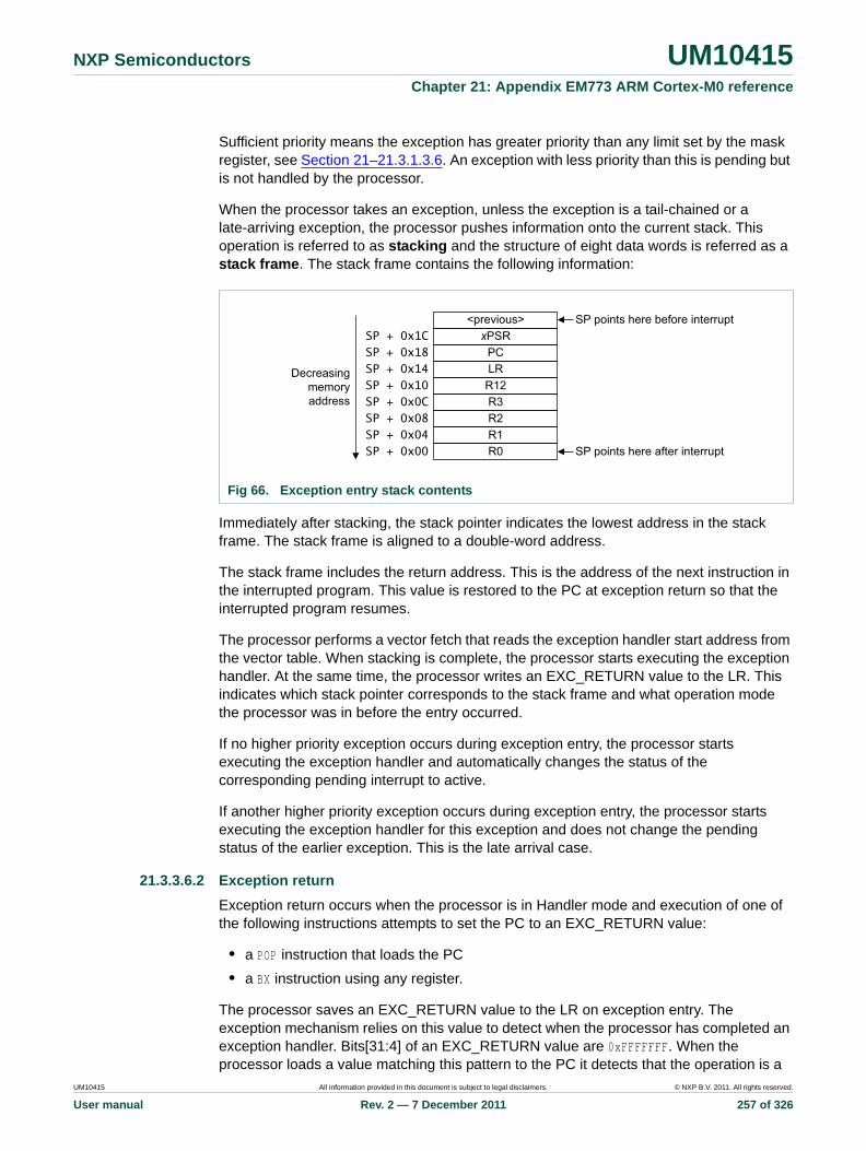
NXP Semiconductors UM10415Chapter 21: Appendix EM773 ARM Cortex-M0 reference
Sufficient priority means the exception has greater priority than any limit set by the mask register, see Section 21–21.3.1.3.6. An exception with less priority than this is pending but is not handled by the processor.
When the processor takes an exception, unless the exception is a tail-chained or a late-arriving exception, the processor pushes information onto the current stack. This operation is referred to as stacking and the structure of eight data words is referred as a stack frame. The stack frame contains the following information:
Immediately after stacking, the stack pointer indicates the lowest address in the stack frame. The stack frame is aligned to a double-word address.
The stack frame includes the return address. This is the address of the next instruction in the interrupted program. This value is restored to the PC at exception return so that the interrupted program resumes.
The processor performs a vector fetch that reads the exception handler start address from the vector table. When stacking is complete, the processor starts executing the exception handler. At the same time, the processor writes an EXC_RETURN value to the LR. This indicates which stack pointer corresponds to the stack frame and what operation mode the processor was in before the entry occurred.
If no higher priority exception occurs during exception entry, the processor starts executing the exception handler and automatically changes the status of the corresponding pending interrupt to active.
If another higher priority exception occurs during exception entry, the processor starts executing the exception handler for this exception and does not change the pending status of the earlier exception. This is the late arrival case.
21.3.3.6.2 Exception return
Exception return occurs when the processor is in Handler mode and execution of one of the following instructions attempts to set the PC to an EXC_RETURN value:
• a POP instruction that loads the PC
• a BX instruction using any register.
The processor saves an EXC_RETURN value to the LR on exception entry. The exception mechanism relies on this value to detect when the processor has completed an exception handler. Bits[31:4] of an EXC_RETURN value are 0xFFFFFFF. When the processor loads a value matching this pattern to the PC it detects that the operation is a
Fig 66. Exception entry stack contents
���*������! � �2 ?�� ���� ��*�������������������
;*� .���@
���*������! � ��?� ����� ��*�
������������������������������������������������������������������������
7 '� ������� ���:��//� ��
UM10415 All information provided in this document is subject to legal disclaimers. © NXP B.V. 2011. All rights reserved.
User manual Rev. 2 — 7 December 2011 257 of 326
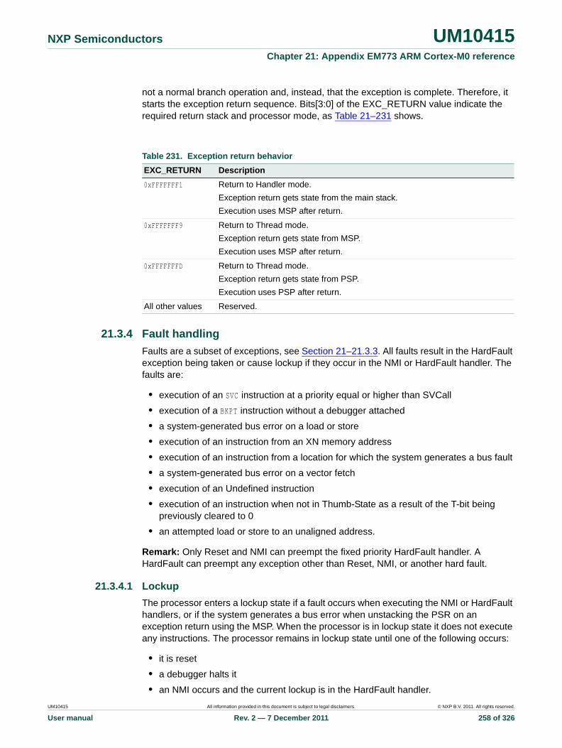
NXP Semiconductors UM10415Chapter 21: Appendix EM773 ARM Cortex-M0 reference
not a normal branch operation and, instead, that the exception is complete. Therefore, it starts the exception return sequence. Bits[3:0] of the EXC_RETURN value indicate the required return stack and processor mode, as Table 21–231 shows.
21.3.4 Fault handling
Faults are a subset of exceptions, see Section 21–21.3.3. All faults result in the HardFault exception being taken or cause lockup if they occur in the NMI or HardFault handler. The faults are:
• execution of an SVC instruction at a priority equal or higher than SVCall
• execution of a BKPT instruction without a debugger attached
• a system-generated bus error on a load or store
• execution of an instruction from an XN memory address
• execution of an instruction from a location for which the system generates a bus fault
• a system-generated bus error on a vector fetch
• execution of an Undefined instruction
• execution of an instruction when not in Thumb-State as a result of the T-bit being previously cleared to 0
• an attempted load or store to an unaligned address.
Remark: Only Reset and NMI can preempt the fixed priority HardFault handler. A HardFault can preempt any exception other than Reset, NMI, or another hard fault.
21.3.4.1 Lockup
The processor enters a lockup state if a fault occurs when executing the NMI or HardFault handlers, or if the system generates a bus error when unstacking the PSR on an exception return using the MSP. When the processor is in lockup state it does not execute any instructions. The processor remains in lockup state until one of the following occurs:
• it is reset
• a debugger halts it
• an NMI occurs and the current lockup is in the HardFault handler.
Table 231. Exception return behavior
EXC_RETURN Description
0xFFFFFFF1 Return to Handler mode.
Exception return gets state from the main stack.
Execution uses MSP after return.
0xFFFFFFF9 Return to Thread mode.
Exception return gets state from MSP.
Execution uses MSP after return.
0xFFFFFFFD Return to Thread mode.
Exception return gets state from PSP.
Execution uses PSP after return.
All other values Reserved.
UM10415 All information provided in this document is subject to legal disclaimers. © NXP B.V. 2011. All rights reserved.
User manual Rev. 2 — 7 December 2011 258 of 326
NXP Semiconductors UM10415Chapter 21: Appendix EM773 ARM Cortex-M0 reference
Remark: If lockup state occurs in the NMI handler a subsequent NMI does not cause the processor to leave lockup state.
21.3.5 Power management
The Cortex-M0 processor sleep modes reduce power consumption:
• a sleep mode, that stops the processor clock
• a Deep-sleep mode (see Section 3.8.3).
The SLEEPDEEP bit of the SCR selects which sleep mode is used, see Section 21–21.5.3.5.
This section describes the mechanisms for entering sleep mode and the conditions for waking up from sleep mode.
21.3.5.1 Entering sleep mode
This section describes the mechanisms software can use to put the processor into sleep mode.
The system can generate spurious wake-up events, for example a debug operation wakes up the processor. Therefore software must be able to put the processor back into sleep mode after such an event. A program might have an idle loop to put the processor back in to sleep mode.
21.3.5.1.1 Wait for interrupt
The Wait For Interrupt instruction, WFI, causes immediate entry to sleep mode. When the processor executes a WFI instruction it stops executing instructions and enters sleep mode. See Section 21–21.4.7.12 for more information.
21.3.5.1.2 Wait for event
Remark: The WFE instruction is not implemented on the EM773.
The Wait For Event instruction, WFE, causes entry to sleep mode conditional on the value of a one-bit event register. When the processor executes a WFE instruction, it checks the value of the event register:
0 — The processor stops executing instructions and enters sleep mode
1 — The processor sets the register to zero and continues executing instructions without entering sleep mode.
See Section 21–21.4.7.11 for more information.
If the event register is 1, this indicates that the processor must not enter sleep mode on execution of a WFE instruction. Typically, this is because of the assertion of an external event, or because another processor in the system has executed a SEV instruction, see Section 21–21.4.7.9. Software cannot access this register directly.
UM10415 All information provided in this document is subject to legal disclaimers. © NXP B.V. 2011. All rights reserved.
User manual Rev. 2 — 7 December 2011 259 of 326
NXP Semiconductors UM10415Chapter 21: Appendix EM773 ARM Cortex-M0 reference
21.3.5.1.3 Sleep-on-exit
If the SLEEPONEXIT bit of the SCR is set to 1, when the processor completes the execution of an exception handler and returns to Thread mode it immediately enters sleep mode. Use this mechanism in applications that only require the processor to run when an interrupt occurs.
21.3.5.2 Wake-up from sleep mode
The conditions for the processor to wake-up depend on the mechanism that caused it to enter sleep mode.
21.3.5.2.1 Wake-up from WFI or sleep-on-exit
Normally, the processor wakes up only when it detects an exception with sufficient priority to cause exception entry.
Some embedded systems might have to execute system restore tasks after the processor wakes up, and before it executes an interrupt handler. To achieve this set the PRIMASK bit to 1. If an interrupt arrives that is enabled and has a higher priority than current exception priority, the processor wakes up but does not execute the interrupt handler until the processor sets PRIMASK to zero. For more information about PRIMASK, see Section 21–21.3.1.3.6.
21.3.5.2.2 Wake-up from WFE
The processor wakes up if:
• it detects an exception with sufficient priority to cause exception entry
• in a multiprocessor system, another processor in the system executes a SEV instruction.
In addition, if the SEVONPEND bit in the SCR is set to 1, any new pending interrupt triggers an event and wakes up the processor, even if the interrupt is disabled or has insufficient priority to cause exception entry. For more information about the SCR see Section 21–21.5.3.5.
21.3.5.3 Power management programming hints
ISO/IEC C cannot directly generate the WFI, WFE, and SEV instructions. The CMSIS provides the following intrinsic functions for these instructions:
void __WFE(void) // Wait for Event
void __WFI(void) // Wait for Interrupt
void __SEV(void) // Send Event
21.4 Instruction set
21.4.1 Instruction set summary
The processor implements a version of the Thumb instruction set. Table 232 lists the supported instructions.
Remark: In Table 232
UM10415 All information provided in this document is subject to legal disclaimers. © NXP B.V. 2011. All rights reserved.
User manual Rev. 2 — 7 December 2011 260 of 326

NXP Semiconductors UM10415Chapter 21: Appendix EM773 ARM Cortex-M0 reference
• angle brackets, <>, enclose alternative forms of the operand
• braces, {}, enclose optional operands and mnemonic parts
• the Operands column is not exhaustive.
For more information on the instructions and operands, see the instruction descriptions.
Table 232. Cortex-M0 instructions
Mnemonic Operands Brief description Flags Reference
ADCS {Rd,} Rn, Rm Add with Carry N,Z,C,V Section 21–21.4.5.1
ADD{S} {Rd,} Rn, <Rm|#imm> Add N,Z,C,V Section 21–21.4.5.1
ADR Rd, label PC-relative Address to Register - Section 21–21.4.4.1
ANDS {Rd,} Rn, Rm Bitwise AND N,Z Section 21–21.4.5.1
ASRS {Rd,} Rm, <Rs|#imm> Arithmetic Shift Right N,Z,C Section 21–21.4.5.3
B{cc} label Branch {conditionally} - Section 21–21.4.6.1
BICS {Rd,} Rn, Rm Bit Clear N,Z Section 21–21.4.5.2
BKPT #imm Breakpoint - Section 21–21.4.7.1
BL label Branch with Link - Section 21–21.4.6.1
BLX Rm Branch indirect with Link - Section 21–21.4.6.1
BX Rm Branch indirect - Section 21–21.4.6.1
CMN Rn, Rm Compare Negative N,Z,C,V Section 21–21.4.5.4
CMP Rn, <Rm|#imm> Compare N,Z,C,V Section 21–21.4.5.4
CPSID i Change Processor State, Disable Interrupts
- Section 21–21.4.7.2
CPSIE i Change Processor State, Enable Interrupts
- Section 21–21.4.7.2
DMB - Data Memory Barrier - Section 21–21.4.7.3
DSB - Data Synchronization Barrier - Section 21–21.4.7.4
EORS {Rd,} Rn, Rm Exclusive OR N,Z Section 21–21.4.5.2
ISB - Instruction Synchronization Barrier - Section 21–21.4.7.5
LDM Rn{!}, reglist Load Multiple registers, increment after - Section 21–21.4.4.5
LDR Rt, label Load Register from PC-relative address - Section 21–21.4.4
LDR Rt, [Rn, <Rm|#imm>] Load Register with word - Section 21–21.4.4
LDRB Rt, [Rn, <Rm|#imm>] Load Register with byte - Section 21–21.4.4
LDRH Rt, [Rn, <Rm|#imm>] Load Register with halfword - Section 21–21.4.4
LDRSB Rt, [Rn, <Rm|#imm>] Load Register with signed byte - Section 21–21.4.4
LDRSH Rt, [Rn, <Rm|#imm>] Load Register with signed halfword - Section 21–21.4.4
LSLS {Rd,} Rn, <Rs|#imm> Logical Shift Left N,Z,C Section 21–21.4.5.3
U {Rd,} Rn, <Rs|#imm> Logical Shift Right N,Z,C Section 21–21.4.5.3
MOV{S} Rd, Rm Move N,Z Section 21–21.4.5.5
MRS Rd, spec_reg Move to general register from special register
- Section 21–21.4.7.6
MSR spec_reg, Rm Move to special register from general register
N,Z,C,V Section 21–21.4.7.7
MULS Rd, Rn, Rm Multiply, 32-bit result N,Z Section 21–21.4.5.6
MVNS Rd, Rm Bitwise NOT N,Z Section 21–21.4.5.5
UM10415 All information provided in this document is subject to legal disclaimers. © NXP B.V. 2011. All rights reserved.
User manual Rev. 2 — 7 December 2011 261 of 326

NXP Semiconductors UM10415Chapter 21: Appendix EM773 ARM Cortex-M0 reference
21.4.2 Intrinsic functions
ISO/IEC C code cannot directly access some Cortex-M0 instructions. This section describes intrinsic functions that can generate these instructions, provided by the CMSIS and that might be provided by a C compiler. If a C compiler does not support an appropriate intrinsic function, you might have to use inline assembler to access the relevant instruction.
The CMSIS provides the following intrinsic functions to generate instructions that ISO/IEC C code cannot directly access:
NOP - No Operation - Section 21–21.4.7.8
ORRS {Rd,} Rn, Rm Logical OR N,Z Section 21–21.4.5.2
POP reglist Pop registers from stack - Section 21–21.4.4.6
PUSH reglist Push registers onto stack - Section 21–21.4.4.6
REV Rd, Rm Byte-Reverse word - Section 21–21.4.5.7
REV16 Rd, Rm Byte-Reverse packed halfwords - Section 21–21.4.5.7
REVSH Rd, Rm Byte-Reverse signed halfword - Section 21–21.4.5.7
RORS {Rd,} Rn, Rs Rotate Right N,Z,C Section 21–21.4.5.3
RSBS {Rd,} Rn, #0 Reverse Subtract N,Z,C,V Section 21–21.4.5.1
SBCS {Rd,} Rn, Rm Subtract with Carry N,Z,C,V Section 21–21.4.5.1
SEV - Send Event - Section 21–21.4.7.9
STM Rn!, reglist Store Multiple registers, increment after - Section 21–21.4.4.5
STR Rt, [Rn, <Rm|#imm>] Store Register as word - Section 21–21.4.4
STRB Rt, [Rn, <Rm|#imm>] Store Register as byte - Section 21–21.4.4
STRH Rt, [Rn, <Rm|#imm>] Store Register as halfword - Section 21–21.4.4
SUB{S} {Rd,} Rn, <Rm|#imm> Subtract N,Z,C,V Section 21–21.4.5.1
SVC #imm Supervisor Call - Section 21–21.4.7.10
SXTB Rd, Rm Sign extend byte - Section 21–21.4.5.8
SXTH Rd, Rm Sign extend halfword - Section 21–21.4.5.8
TST Rn, Rm Logical AND based test N,Z Section 21–21.4.5.9
UXTB Rd, Rm Zero extend a byte - Section 21–21.4.5.8
UXTH Rd, Rm Zero extend a halfword - Section 21–21.4.5.8
WFE - Wait For Event - Section 21–21.4.7.11
WFI - Wait For Interrupt - Section 21–21.4.7.12
Table 232. Cortex-M0 instructions
Mnemonic Operands Brief description Flags Reference
Table 233. CMSIS intrinsic functions to generate some Cortex-M0 instructions
Instruction CMSIS intrinsic function
CPSIE i void __enable_irq(void)
CPSID i void __disable_irq(void)
ISB void __ISB(void)
DSB void __DSB(void)
DMB void __DMB(void)
NOP void __NOP(void)
UM10415 All information provided in this document is subject to legal disclaimers. © NXP B.V. 2011. All rights reserved.
User manual Rev. 2 — 7 December 2011 262 of 326
NXP Semiconductors UM10415Chapter 21: Appendix EM773 ARM Cortex-M0 reference
The CMSIS also provides a number of functions for accessing the special registers using MRS and MSR instructions:
21.4.3 About the instruction descriptions
The following sections give more information about using the instructions:
• Section 21.4.3.1 “Operands”
• Section 21.4.3.2 “Restrictions when using PC or SP”
• Section 21.4.3.3 “Shift Operations”
• Section 21.4.3.4 “Address alignment”
• Section 21.4.3.5 “PC-relative expressions”
• Section 21.4.3.6 “Conditional execution”.
21.4.3.1 Operands
An instruction operand can be an ARM register, a constant, or another instruction-specific parameter. Instructions act on the operands and often store the result in a destination register. When there is a destination register in the instruction, it is usually specified before the other operands.
21.4.3.2 Restrictions when using PC or SP
Many instructions are unable to use, or have restrictions on whether you can use, the Program Counter (PC) or Stack Pointer (SP) for the operands or destination register. See instruction descriptions for more information.
REV uint32_t __REV(uint32_t int value)
REV16 uint32_t __REV16(uint32_t int value)
REVSH uint32_t __REVSH(uint32_t int value)
SEV void __SEV(void)
WFE void __WFE(void)
WFI void __WFI(void)
Table 234. insic functions to access the special registers
Special register Access CMSIS function
PRIMASK Read uint32_t __get_PRIMASK (void)
Write void __set_PRIMASK (uint32_t value)
CONTROL Read uint32_t __get_CONTROL (void)
Write void __set_CONTROL (uint32_t value)
MSP Read uint32_t __get_MSP (void)
Write void __set_MSP (uint32_t TopOfMainStack)
PSP Read uint32_t __get_PSP (void)
Write void __set_PSP (uint32_t TopOfProcStack)
Table 233. CMSIS intrinsic functions to generate some Cortex-M0 instructions
Instruction CMSIS intrinsic function
UM10415 All information provided in this document is subject to legal disclaimers. © NXP B.V. 2011. All rights reserved.
User manual Rev. 2 — 7 December 2011 263 of 326
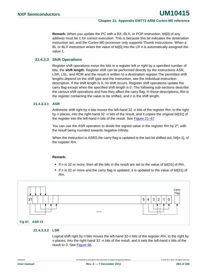
NXP Semiconductors UM10415Chapter 21: Appendix EM773 ARM Cortex-M0 reference
Remark: When you update the PC with a BX, BLX, or POP instruction, bit[0] of any address must be 1 for correct execution. This is because this bit indicates the destination instruction set, and the Cortex-M0 processor only supports Thumb instructions. When a BL or BLX instruction writes the value of bit[0] into the LR it is automatically assigned the value 1.
21.4.3.3 Shift Operations
Register shift operations move the bits in a register left or right by a specified number of bits, the shift length. Register shift can be performed directly by the instructions ASR, LSR, LSL, and ROR and the result is written to a destination register.The permitted shift lengths depend on the shift type and the instruction, see the individual instruction description. If the shift length is 0, no shift occurs. Register shift operations update the carry flag except when the specified shift length is 0. The following sub-sections describe the various shift operations and how they affect the carry flag. In these descriptions, Rm is the register containing the value to be shifted, and n is the shift length.
21.4.3.3.1 ASR
Arithmetic shift right by n bits moves the left-hand 32 -n bits of the register Rm, to the right by n places, into the right-hand 32 -n bits of the result, and it copies the original bit[31] of the register into the left-hand n bits of the result. See Figure 21–67.
You can use the ASR operation to divide the signed value in the register Rm by 2n, with the result being rounded towards negative-infinity.
When the instruction is ASRS the carry flag is updated to the last bit shifted out, bit[n-1], of the register Rm.
Remark:
• If n is 32 or more, then all the bits in the result are set to the value of bit[31] of Rm.
• If n is 32 or more and the carry flag is updated, it is updated to the value of bit[31] of Rm.
21.4.3.3.2 LSR
Logical shift right by n bits moves the left-hand 32-n bits of the register Rm, to the right by n places, into the right-hand 32 -n bits of the result, and it sets the left-hand n bits of the result to 0. See Figure 68.
Fig 67. ASR #3
�� � ���� �
555
���:=)��
UM10415 All information provided in this document is subject to legal disclaimers. © NXP B.V. 2011. All rights reserved.
User manual Rev. 2 — 7 December 2011 264 of 326
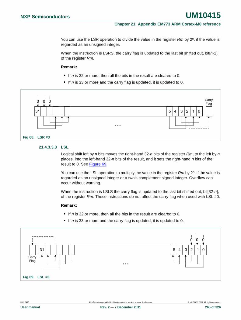
NXP Semiconductors UM10415Chapter 21: Appendix EM773 ARM Cortex-M0 reference
You can use the LSR operation to divide the value in the register Rm by 2n, if the value is regarded as an unsigned integer.
When the instruction is LSRS, the carry flag is updated to the last bit shifted out, bit[n-1], of the register Rm.
Remark:
• If n is 32 or more, then all the bits in the result are cleared to 0.
• If n is 33 or more and the carry flag is updated, it is updated to 0.
21.4.3.3.3 LSL
Logical shift left by n bits moves the right-hand 32-n bits of the register Rm, to the left by n places, into the left-hand 32-n bits of the result, and it sets the right-hand n bits of the result to 0. See Figure 69.
You can use the LSL operation to multiply the value in the register Rm by 2n, if the value is regarded as an unsigned integer or a two’s complement signed integer. Overflow can occur without warning.
When the instruction is LSLS the carry flag is updated to the last bit shifted out, bit[32-n], of the register Rm. These instructions do not affect the carry flag when used with LSL #0.
Remark:
• If n is 32 or more, then all the bits in the result are cleared to 0.
• If n is 33 or more and the carry flag is updated, it is updated to 0.
Fig 68. LSR #3
�� � ���� �
555
��� ���:=)��
Fig 69. LSL #3
� ���� ���
555
� � �
���:=)��
UM10415 All information provided in this document is subject to legal disclaimers. © NXP B.V. 2011. All rights reserved.
User manual Rev. 2 — 7 December 2011 265 of 326

NXP Semiconductors UM10415Chapter 21: Appendix EM773 ARM Cortex-M0 reference
21.4.3.3.4 ROR
Rotate right by n bits moves the left-hand 32-n bits of the register Rm, to the right by n places, into the right-hand 32-n bits of the result, and it moves the right-hand n bits of the register into the left-hand n bits of the result. See Figure 21–70.
When the instruction is RORS the carry flag is updated to the last bit rotation, bit[n-1], of the register Rm.
Remark:
• If n is 32, then the value of the result is same as the value in Rm, and if the carry flag is updated, it is updated to bit[31] of Rm.
• ROR
with shift length, n, greater than 32 is the same as
ROR
with shift length n-32.
21.4.3.4 Address alignment
An aligned access is an operation where a word-aligned address is used for a word, or multiple word access, or where a halfword-aligned address is used for a halfword access. Byte accesses are always aligned.
There is no support for unaligned accesses on the Cortex-M0 processor. Any attempt to perform an unaligned memory access operation results in a HardFault exception.
21.4.3.5 PC-relative expressions
A PC-relative expression or label is a symbol that represents the address of an instruction or literal data. It is represented in the instruction as the PC value plus or minus a numeric offset. The assembler calculates the required offset from the label and the address of the current instruction. If the offset is too big, the assembler produces an error.
Remark:
• For most instructions, the value of the PC is the address of the current instruction plus 4 bytes.
• Your assembler might permit other syntaxes for PC-relative expressions, such as a label plus or minus a number, or an expression of the form [PC, #imm].
Fig 70. ROR #3
�� � ���� �
555
���:=)��
UM10415 All information provided in this document is subject to legal disclaimers. © NXP B.V. 2011. All rights reserved.
User manual Rev. 2 — 7 December 2011 266 of 326

NXP Semiconductors UM10415Chapter 21: Appendix EM773 ARM Cortex-M0 reference
21.4.3.6 Conditional execution
Most data processing instructions update the condition flags in the Application Program Status Register (APSR) according to the result of the operation, see Section . Some instructions update all flags, and some only update a subset. If a flag is not updated, the original value is preserved. See the instruction descriptions for the flags they affect.
You can execute a conditional branch instruction, based on the condition flags set in another instruction, either:
• immediately after the instruction that updated the flags
• after any number of intervening instructions that have not updated the flags.
On the Cortex-M0 processor, conditional execution is available by using conditional branches.
This section describes:
• Section 21.4.3.6.1 “The condition flags”
• Section 21.4.3.6.2 “Condition code suffixes”.
21.4.3.6.1 The condition flags
The APSR contains the following condition flags:
N — Set to 1 when the result of the operation was negative, cleared to 0 otherwise.
Z — Set to 1 when the result of the operation was zero, cleared to 0 otherwise.
C — Set to 1 when the operation resulted in a carry, cleared to 0 otherwise.
V — Set to 1 when the operation caused overflow, cleared to 0 otherwise.
For more information about the APSR see Section 21–21.3.1.3.5.
A carry occurs:
• if the result of an addition is greater than or equal to 232
• if the result of a subtraction is positive or zero
• as the result of a shift or rotate instruction.
Overflow occurs when the sign of the result, in bit[31], does not match the sign of the result had the operation been performed at infinite precision, for example:
• if adding two negative values results in a positive value
• if adding two positive values results in a negative value
• if subtracting a positive value from a negative value generates a positive value
• if subtracting a negative value from a positive value generates a negative value.
The Compare operations are identical to subtracting, for CMP, or adding, for CMN, except that the result is discarded. See the instruction descriptions for more information.
21.4.3.6.2 Condition code suffixes
Conditional branch is shown in syntax descriptions as B{cond}. A branch instruction with a condition code is only taken if the condition code flags in the APSR meet the specified condition, otherwise the branch instruction is ignored. shows the condition codes to use.
UM10415 All information provided in this document is subject to legal disclaimers. © NXP B.V. 2011. All rights reserved.
User manual Rev. 2 — 7 December 2011 267 of 326
NXP Semiconductors UM10415Chapter 21: Appendix EM773 ARM Cortex-M0 reference
Table 235 also shows the relationship between condition code suffixes and the N, Z, C, and V flags.
21.4.4 Memory access instructions
Table 236 shows the memory access instructions:
21.4.4.1 ADR
Generates a PC-relative address.
21.4.4.1.1 Syntax
ADR Rd, label
Table 235. Condition code suffixes
Suffix Flags Meaning
EQ Z = 1 Equal, last flag setting result was zero
NE Z = 0 Not equal, last flag setting result was non-zero
CS or HS C = 1 Higher or same, unsigned
CC or LO C = 0 Lower, unsigned
MI N = 1 Negative
PL N = 0 Positive or zero
VS V = 1 Overflow
VC V = 0 No overflow
HI C = 1 and Z = 0 Higher, unsigned
LS C = 0 or Z = 1 Lower or same, unsigned
GE N = V Greater than or equal, signed
LT N = V Less than, signed
GT Z = 0 and N = V Greater than, signed
LE Z = 1 and N = V Less than or equal, signed
AL Can have any value Always. This is the default when no suffix is specified.
Table 236. Access instructions
Mnemonic Brief description See
LDR{type} Load Register using register offset Section 21–21.4.4.3
LDR Load Register from PC-relative address Section 21–21.4.4.4
POP Pop registers from stack Section 21–21.4.4.6
PUSH Push registers onto stack Section 21–21.4.4.6
STM Store Multiple registers Section 21–21.4.4.5
STR{type} Store Register using immediate offset Section 21–21.4.4.2
STR{type} Store Register using register offset Section 21–21.4.4.3
UM10415 All information provided in this document is subject to legal disclaimers. © NXP B.V. 2011. All rights reserved.
User manual Rev. 2 — 7 December 2011 268 of 326
NXP Semiconductors UM10415Chapter 21: Appendix EM773 ARM Cortex-M0 reference
where:
Rd is the destination register.
label is a PC-relative expression. See Section 21–21.4.3.5.
21.4.4.1.2 Operation
ADR generates an address by adding an immediate value to the PC, and writes the result to the destination register.
ADR facilitates the generation of position-independent code, because the address is PC-relative.
If you use ADR to generate a target address for a BX or BLX instruction, you must ensure that bit[0] of the address you generate is set to 1 for correct execution.
21.4.4.1.3 Restrictions
In this instruction Rd must specify R0-R7. The data-value addressed must be word aligned and within 1020 bytes of the current PC.
21.4.4.1.4 Condition flags
This instruction does not change the flags.
21.4.4.1.5 Examples
ADR R1, TextMessage ; Write address value of a location labelled as; TextMessage to R1
ADR R3, [PC,#996] ; Set R3 to value of PC + 996.
21.4.4.2 LDR and STR, immediate offset
Load and Store with immediate offset.
21.4.4.2.1 Syntax
LDR Rt, [<Rn | SP> {, #imm}]
LDR<B|H> Rt, [Rn {, #imm}]
STR Rt, [<Rn | SP>, {,#imm}]
STR<B|H> Rt, [Rn {,#imm}]
where:
Rt is the register to load or store.
Rn is the register on which the memory address is based.
imm is an offset from Rn. If imm is omitted, it is assumed to be zero.
21.4.4.2.2 Operation
LDR, LDRB and LDRH instructions load the register specified by Rt with either a word, byte or halfword data value from memory. Sizes less than word are zero extended to 32-bits before being written to the register specified by Rt.
UM10415 All information provided in this document is subject to legal disclaimers. © NXP B.V. 2011. All rights reserved.
User manual Rev. 2 — 7 December 2011 269 of 326

NXP Semiconductors UM10415Chapter 21: Appendix EM773 ARM Cortex-M0 reference
STR, STRB and STRH instructions store the word, least-significant byte or lower halfword contained in the single register specified by Rt in to memory. The memory address to load from or store to is the sum of the value in the register specified by either Rn or SP and the immediate value imm.
21.4.4.2.3 Restrictions
In these instructions:
• Rt and Rn must only specify R0-R7.
• imm must be between:
– 0 and 1020 and an integer multiple of four for LDR and STR
using SP as the base register
– 0 and 124 and an integer multiple of four for LDR and STR
using R0-R7 as the base register
– 0 and 62 and an integer multiple of two for LDRH and STRH
– 0 and 31 for LDRB and STRB.
• The computed address must be divisible by the number of bytes in the transaction, see Section 21–21.4.3.4.
21.4.4.2.4 Condition flags
These instructions do not change the flags.
21.4.4.2.5 Examples
LDR R4, [R7 ; Loads R4 from the address in R7.STR R2, [R0,#const-struc] ; const-struc is an expression evaluating
; to a constant in the range 0-1020.
21.4.4.3 LDR and STR, register offset
Load and Store with register offset.
21.4.4.3.1 Syntax
LDR Rt, [Rn, Rm]
LDR<B|H> Rt, [Rn, Rm]
LDR<SB|SH> Rt, [Rn, Rm]
STR Rt, [Rn, Rm]
STR<B|H> Rt, [Rn, Rm]
where:
Rt is the register to load or store.
Rn is the register on which the memory address is based.
Rm is a register containing a value to be used as the offset.
UM10415 All information provided in this document is subject to legal disclaimers. © NXP B.V. 2011. All rights reserved.
User manual Rev. 2 — 7 December 2011 270 of 326

NXP Semiconductors UM10415Chapter 21: Appendix EM773 ARM Cortex-M0 reference
21.4.4.3.2 Operation
LDR, LDRB, U, LDRSB and LDRSH load the register specified by Rt with either a word, zero extended byte, zero extended halfword, sign extended byte or sign extended halfword value from memory.
STR, STRB and STRH store the word, least-significant byte or lower halfword contained in the single register specified by Rt into memory.
The memory address to load from or store to is the sum of the values in the registers specified by Rn and Rm.
21.4.4.3.3 Restrictions
In these instructions:
• Rt, Rn, and Rm must only specify R0-R7.
• the computed memory address must be divisible by the number of bytes in the load or store, see Section 21–21.4.3.4.
21.4.4.3.4 Condition flags
These instructions do not change the flags.
21.4.4.3.5 Examples
STR R0, [R5, R1] ; Store value of R0 into an address equal to; sum of R5 and R1
LDRSH R1, [R2, R3] ; Load a halfword from the memory address; specified by (R2 + R3), sign extend to 32-bits
; and write to R1.
21.4.4.4 LDR, PC-relative
Load register (literal) from memory.
21.4.4.4.1 Syntax
LDR Rt, label
where:
Rt is the register to load.
label is a PC-relative expression. See Section 21–21.4.3.5.
21.4.4.4.2 Operation
Loads the register specified by Rt from the word in memory specified by label.
21.4.4.4.3 Restrictions
In these instructions, label must be within 1020 bytes of the current PC and word aligned.
21.4.4.4.4 Condition flags
These instructions do not change the flags.
UM10415 All information provided in this document is subject to legal disclaimers. © NXP B.V. 2011. All rights reserved.
User manual Rev. 2 — 7 December 2011 271 of 326

NXP Semiconductors UM10415Chapter 21: Appendix EM773 ARM Cortex-M0 reference
21.4.4.4.5 Examples
LDR R0, LookUpTable ; Load R0 with a word of data from an address; labelled as LookUpTable.
LDR R3, [PC, #100] ; Load R3 with memory word at (PC + 100).
21.4.4.5 LDM and STM
Load and Store Multiple registers.
21.4.4.5.1 Syntax
LDM Rn{!}, reglist
STM Rn!, reglist
where:
Rn is the register on which the memory addresses are based.
! writeback suffix.
reglist is a list of one or more registers to be loaded or stored, enclosed in braces. It can contain register ranges. It must be comma separated if it contains more than one register or register range, see Section 21–21.4.4.5.5.
LDMIA and LDMFD are synonyms for LDM. LDMIA refers to the base register being Incremented After each access. LDMFD refers to its use for popping data from Full Descending stacks.
STMIA and STMEA are synonyms for STM. STMIA refers to the base register being Incremented After each access. STMEA refers to its use for pushing data onto Empty Ascending stacks.
21.4.4.5.2 Operation
LDM instructions load the registers in reglist with word values from memory addresses based on Rn.
STM instructions store the word values in the registers in reglist to memory addresses based on Rn.
The memory addresses used for the accesses are at 4-byte intervals ranging from the value in the register specified by Rn to the value in the register specified by Rn + 4 * (n-1), where n is the number of registers in reglist. The accesses happens in order of increasing register numbers, with the lowest numbered register using the lowest memory address and the highest number register using the highest memory address. If the writeback suffix is specified, the value in the register specified by Rn + 4 *n is written back to the register specified by Rn.
21.4.4.5.3 Restrictions
In these instructions:
• reglist and Rn are limited to R0-R7.
• the writeback suffix must always be used unless the instruction is an LDM where reglist also contains Rn, in which case the writeback suffix must not be used.
UM10415 All information provided in this document is subject to legal disclaimers. © NXP B.V. 2011. All rights reserved.
User manual Rev. 2 — 7 December 2011 272 of 326

NXP Semiconductors UM10415Chapter 21: Appendix EM773 ARM Cortex-M0 reference
• the value in the register specified by Rn must be word aligned. See Section 21–21.4.3.4 for more information.
• for STM, if Rn appears in reglist, then it must be the first register in the list.
21.4.4.5.4 Condition flags
These instructions do not change the flags.
21.4.4.5.5 Examples
LDM R0,{R0,R3,R4} ; LDMIA is a synonym for LDMSTMIA R1!,{R2-R4,R6}
21.4.4.5.6 Incorrect examples
STM R5!,{R4,R5,R6} ; Value stored for R5 is unpredictable LDM R2,{} ; There must be at least one register in the list
21.4.4.6 PUSH and POP
Push registers onto, and pop registers off a full-descending stack.
21.4.4.6.1 Syntax
PUSH reglist
POP reglist
where:
reglist is a non-empty list of registers, enclosed in braces. It can contain register ranges. It must be comma separated if it contains more than one register or register range.
21.4.4.6.2 Operation
PUSH stores registers on the stack, with the lowest numbered register using the lowest memory address and the highest numbered register using the highest memory address.
POP loads registers from the stack, with the lowest numbered register using the lowest memory address and the highest numbered register using the highest memory address.
PUSH uses the value in the SP register minus four as the highest memory address,
POP uses the value in the SP register as the lowest memory address, implementing a full-descending stack. On completion,
PUSH updates the SP register to point to the location of the lowest store value,
POP updates the SP register to point to the location above the highest location loaded.
If a POP instruction includes PC in its reglist, a branch to this location is performed when the POP instruction has completed. Bit[0] of the value read for the PC is used to update the APSR T-bit. This bit must be 1 to ensure correct operation.
21.4.4.6.3 Restrictions
In these instructions:
• reglist must use only R0-R7.
UM10415 All information provided in this document is subject to legal disclaimers. © NXP B.V. 2011. All rights reserved.
User manual Rev. 2 — 7 December 2011 273 of 326

NXP Semiconductors UM10415Chapter 21: Appendix EM773 ARM Cortex-M0 reference
• The exception is LR for a PUSH and PC for a POP.
21.4.4.6.4 Condition flags
These instructions do not change the flags.
21.4.4.6.5 Examples
PUSH {R0,R4-R7} ; Push R0,R4,R5,R6,R7 onto the stackPUSH {R2,LR} ; Push R2 and the link-register onto the stackPOP {R0,R6,PC} ; Pop r0,r6 and PC from the stack, then branch to
; the new PC.
21.4.5 General data processing instructions
Table 237 shows the data processing instructions:
Table 237. Data processing instructions
Mnemonic Brief description See
ADCS Add with Carry Section 21–21.4.5.1
ADD{S} Add Section 21–21.4.5.1
ANDS Logical AND Section 21–21.4.5.2
ASRS Arithmetic Shift Right Section 21–21.4.5.3
BICS Bit Clear Section 21–21.4.5.2
CMN Compare Negative Section 21–21.4.5.4
CMP Compare Section 21–21.4.5.4
EORS Exclusive OR Section 21–21.4.5.2
LSLS Logical Shift Left Section 21–21.4.5.3
LSRS Logical Shift Right Section 21–21.4.5.3
MOV{S} Move Section 21–21.4.5.5
MULS Multiply Section 21–21.4.5.6
MVNS Move NOT Section 21–21.4.5.5
ORRS Logical OR Section 21–21.4.5.2
REV Reverse byte order in a word Section 21–21.4.5.7
REV16 Reverse byte order in each halfword Section 21–21.4.5.7
REVSH Reverse byte order in bottom halfword and sign extend
Section 21–21.4.5.7
RORS Rotate Right Section 21–21.4.5.3
RSBS Reverse Subtract Section 21–21.4.5.1
SBCS Subtract with Carry Section 21–21.4.5.1
SUBS Subtract Section 21–21.4.5.1
SXTB Sign extend a byte Section 21–21.4.5.8
SXTH Sign extend a halfword Section 21–21.4.5.8
UXTB Zero extend a byte Section 21–21.4.5.8
UXTH Zero extend a halfword Section 21–21.4.5.8
TST Test Section 21–21.4.5.9
UM10415 All information provided in this document is subject to legal disclaimers. © NXP B.V. 2011. All rights reserved.
User manual Rev. 2 — 7 December 2011 274 of 326
NXP Semiconductors UM10415Chapter 21: Appendix EM773 ARM Cortex-M0 reference
21.4.5.1 ADC, ADD, RSB, SBC, and SUB
Add with carry, Add, Reverse Subtract, Subtract with carry, and Subtract.
21.4.5.1.1 Syntax
ADCS {Rd,} Rn, Rm
ADD{S} {Rd,} Rn, <Rm|#imm>
RSBS {Rd,} Rn, Rm, #0
SBCS {Rd,} Rn, Rm
SUB{S} {Rd,} Rn,
<Rm|#imm>
Where:
S causes an ADD or SUB instruction to update flags
Rd specifies the result register
Rn specifies the first source register
Rm specifies the second source register
imm specifies a constant immediate value.
When the optional Rd register specifier is omitted, it is assumed to take the same value as Rn, for example ADDS R1,R2 is identical to ADDS R1,R1,R2.
21.4.5.1.2 Operation
The ADCS instruction adds the value in Rn to the value in Rm, adding a further one if the carry flag is set, places the result in the register specified by Rd and updates the N, Z, C, and V flags.
The ADD instruction adds the value in Rn to the value in Rm or an immediate value specified by imm and places the result in the register specified by Rd.
The ADDS instruction performs the same operation as ADD and also updates the N, Z, C and V flags.
The RSBS instruction subtracts the value in Rn from zero, producing the arithmetic negative of the value, and places the result in the register specified by Rd and updates the N, Z, C and V flags.
The SBCS instruction subtracts the value of Rm from the value in Rn, deducts a further one if the carry flag is set. It places the result in the register specified by Rd and updates the N, Z, C and V flags.
The SUB instruction subtracts the value in Rm or the immediate specified by imm. It places the result in the register specified by Rd.
The SUBS instruction performs the same operation as SUB and also updates the N, Z, C and V flags.
Use ADC and SBC to synthesize multiword arithmetic, see Section 21.4.5.1.4.
UM10415 All information provided in this document is subject to legal disclaimers. © NXP B.V. 2011. All rights reserved.
User manual Rev. 2 — 7 December 2011 275 of 326
NXP Semiconductors UM10415Chapter 21: Appendix EM773 ARM Cortex-M0 reference
See also Section 21–21.4.4.1.
21.4.5.1.3 Restrictions
Table 238 lists the legal combinations of register specifiers and immediate values that can be used with each instruction.
21.4.5.1.4 Examples
The following shows two instructions that add a 64-bit integer contained in R0 and R1 to another 64-bit integer contained in R2 and R3, and place the result in R0 and R1.
64-bit addition:
ADDS R0, R0, R2 ; add the least significant wordsADCS R1, R1, R3 ; add the most significant words with carry
Multiword values do not have to use consecutive registers. The following shows instructions that subtract a 96-bit integer contained in R1, R2, and R3 from another contained in R4, R5, and R6. The example stores the result in R4, R5, and R6.
96-bit subtraction:
SUBS R4, R4, R1 ; subtract the least significant wordsSBCS R5, R5, R2 ; subtract the middle words with carrySBCS R6, R6, R3 ; subtract the most significant words with carry
The following shows the RSBS instruction used to perform a 1's complement of a single register.
Arithmetic negation: RSBS R7, R7, #0 ; subtract R7 from zero
21.4.5.2 AND, ORR, EOR, and BIC
Logical AND, OR, Exclusive OR, and Bit Clear.
Table 238. ADC, ADD, RSB, SBC and SUB operand restrictions
Instruction Rd Rn Rm imm Restrictions
ADCS R0-R7 R0-R7 R0-R7 - Rd and Rn must specify the same register.
ADD R0-R15 R0-R15 R0-PC - Rd and Rn must specify the same register.
Rn and Rm must not both specify PC.
R0-R7 SP or PC - 0-1020 Immediate value must be an integer multiple of four.
SP SP - 0-508 Immediate value must be an integer multiple of four.
ADDS R0-R7 R0-R7 - 0-7 -
R0-R7 R0-R7 - 0-255 Rd and Rn must specify the same register.
R0-R7 R0-R7 R0-R7 - -
RSBS R0-R7 R0-R7 - - -
SBCS R0-R7 R0-R7 R0-R7 - Rd and Rn must specify the same register.
SUB SP SP - 0-508 Immediate value must be an integer multiple of four.
SUBS R0-R7 R0-R7 - 0-7 -
R0-R7 R0-R7 - 0-255 Rd and Rn must specify the same register.
R0-R7 R0-R7 R0-R7 - -
UM10415 All information provided in this document is subject to legal disclaimers. © NXP B.V. 2011. All rights reserved.
User manual Rev. 2 — 7 December 2011 276 of 326

NXP Semiconductors UM10415Chapter 21: Appendix EM773 ARM Cortex-M0 reference
21.4.5.2.1 Syntax
ANDS {Rd,} Rn, Rm
ORRS {Rd,} Rn, Rm
EORS {Rd,} Rn, Rm
BICS {Rd,} Rn, Rm
where:
Rd is the destination register.
Rn is the register holding the first operand and is the same as the destination register.
Rm second register.
21.4.5.2.2 Operation
The AND, EOR, and ORR instructions perform bitwise AND, exclusive OR, and inclusive OR operations on the values in Rn and Rm.
The BIC instruction performs an AND operation on the bits in Rn with the logical negation of the corresponding bits in the value of Rm.
The condition code flags are updated on the result of the operation, see Section 21.4.3.6.1.
21.4.5.2.3 Restrictions
In these instructions, Rd, Rn, and Rm must only specify R0-R7.
21.4.5.2.4 Condition flags
These instructions:
• update the N and Z flags according to the result
• do not affect the C or V flag.
21.4.5.2.5 Examples
ANDS R2, R2, R1ORRS R2, R2, R5ANDS R5, R5, R8EORS R7, R7, R6BICS R0, R0, R1
21.4.5.3 ASR, LSL, LSR, and ROR
Arithmetic Shift Right, Logical Shift Left, Logical Shift Right, and Rotate Right.
21.4.5.3.1 Syntax
ASRS {Rd,} Rm, Rs
ASRS {Rd,} Rm, #imm
LSLS {Rd,} Rm, Rs
LSLS {Rd,} Rm, #imm
UM10415 All information provided in this document is subject to legal disclaimers. © NXP B.V. 2011. All rights reserved.
User manual Rev. 2 — 7 December 2011 277 of 326
NXP Semiconductors UM10415Chapter 21: Appendix EM773 ARM Cortex-M0 reference
LSRS {Rd,} Rm, Rs
LSRS {Rd,} Rm, #imm
RORS {Rd,} Rm, Rs
where:
Rd is the destination register. If Rd is omitted, it is assumed to take the same value as Rm.
Rm is the register holding the value to be shifted.
Rs is the register holding the shift length to apply to the value in Rm.
imm is the shift length.
The range of shift length depends on the instruction:
ASR — shift length from 1 to 32
LSL — shift length from 0 to 31
LSR — shift length from 1 to 32.
Remark: MOVS Rd, Rm is a pseudonym for LSLS Rd, Rm, #0.
21.4.5.3.2 Operation
ASR, LSL, LSR, and ROR perform an arithmetic-shift-left, logical-shift-left, logical-shift-right or a right-rotation of the bits in the register Rm by the number of places specified by the immediate imm or the value in the least-significant byte of the register specified by Rs.
For details on what result is generated by the different instructions, see Section 21–21.4.3.3.
21.4.5.3.3 Restrictions
In these instructions, Rd, Rm, and Rs must only specify R0-R7. For non-immediate instructions, Rd and Rm must specify the same register.
21.4.5.3.4 Condition flags
These instructions update the N and Z flags according to the result.
The C flag is updated to the last bit shifted out, except when the shift length is 0, see Section 21–21.4.3.3. The V flag is left unmodified.
21.4.5.3.5 Examples
ASRS R7, R5, #9 ; Arithmetic shift right by 9 bitsLSLS R1, R2, #3 ; Logical shift left by 3 bits with flag updateLSRS R4, R5, #6 ; Logical shift right by 6 bitsRORS R4, R4, R6 ; Rotate right by the value in the bottom byte of R6.
21.4.5.4 CMP and CMN
Compare and Compare Negative.
UM10415 All information provided in this document is subject to legal disclaimers. © NXP B.V. 2011. All rights reserved.
User manual Rev. 2 — 7 December 2011 278 of 326

NXP Semiconductors UM10415Chapter 21: Appendix EM773 ARM Cortex-M0 reference
21.4.5.4.1 Syntax
CMN Rn, Rm
CMP Rn, #imm
CMP Rn, Rm
where:
Rn is the register holding the first operand.
Rm is the register to compare with.
imm is the immediate value to compare with.
21.4.5.4.2 Operation
These instructions compare the value in a register with either the value in another register or an immediate value. They update the condition flags on the result, but do not write the result to a register.
The CMP instruction subtracts either the value in the register specified by Rm, or the immediate imm from the value in Rn and updates the flags. This is the same as a SUBS instruction, except that the result is discarded.
The CMN instruction adds the value of Rm to the value in Rn and updates the flags. This is the same as an ADDS instruction, except that the result is discarded.
21.4.5.4.3 Restrictions
For the:
• CMN
instruction Rn, and Rm must only specify R0-R7.
• CMP instruction:
– Rn and Rm can specify R0-R14
– immediate must be in the range 0-255.
21.4.5.4.4 Condition flags
These instructions update the N, Z, C and V flags according to the result.
21.4.5.4.5 Examples
CMP R2, R9CMN R0, R2
21.4.5.5 MOV and MVN
Move and Move NOT.
21.4.5.5.1 Syntax
MOV{S} Rd, Rm
MOVS Rd, #imm
UM10415 All information provided in this document is subject to legal disclaimers. © NXP B.V. 2011. All rights reserved.
User manual Rev. 2 — 7 December 2011 279 of 326

NXP Semiconductors UM10415Chapter 21: Appendix EM773 ARM Cortex-M0 reference
MVNS Rd, Rm
where:
S is an optional suffix. If S is specified, the condition code flags are updated on the result of the operation, see Section 21–21.4.3.6.
Rd is the destination register.
Rm is a register.
imm is any value in the range 0-255.
21.4.5.5.2 Operation
The MOV instruction copies the value of Rm into Rd.
The MOVS instruction performs the same operation as the MOV instruction, but also updates the N and Z flags.
The MVNS instruction takes the value of Rm, performs a bitwise logical negate operation on the value, and places the result into Rd.
21.4.5.5.3 Restrictions
In these instructions, Rd, and Rm must only specify R0-R7.
When Rd is the PC in a MOV instruction:
• Bit[0] of the result is discarded.
• A branch occurs to the address created by forcing bit[0] of the result to 0. The T-bit remains unmodified.
Remark: Though it is possible to use MOV as a branch instruction, ARM strongly recommends the use of a BX or BLX instruction to branch for software portability.
21.4.5.5.4 Condition flags
If S is specified, these instructions:
• update the N and Z flags according to the result
• do not affect the C or V flags.
21.4.5.5.5 Example
MOVS R0, #0x000B ; Write value of 0x000B to R0, flags get updatedMOVS R1, #0x0 ; Write value of zero to R1, flags are updatedMOV R10, R12 ; Write value in R12 to R10, flags are not updatedMOVS R3, #23 ; Write value of 23 to R3MOV R8, SP ; Write value of stack pointer to R8MVNS R2, R0 ; Write inverse of R0 to the R2 and update flags
21.4.5.6 MULS
Multiply using 32-bit operands, and producing a 32-bit result.
21.4.5.6.1 Syntax
MULS Rd, Rn, Rm
UM10415 All information provided in this document is subject to legal disclaimers. © NXP B.V. 2011. All rights reserved.User manual Rev. 2 — 7 December 2011 280 of 326

NXP Semiconductors UM10415Chapter 21: Appendix EM773 ARM Cortex-M0 reference
where:
Rd is the destination register.
Rn, Rm are registers holding the values to be multiplied.
21.4.5.6.2 Operation
The MUL instruction multiplies the values in the registers specified by Rn and Rm, and places the least significant 32 bits of the result in Rd. The condition code flags are updated on the result of the operation, see Section 21–21.4.3.6.
The results of this instruction does not depend on whether the operands are signed or unsigned.
21.4.5.6.3 Restrictions
In this instruction:
• Rd, Rn, and Rm must only specify R0-R7
• Rd must be the same as Rm.
21.4.5.6.4 Condition flags
This instruction:
• updates the N and Z flags according to the result
• does not affect the C or V flags.
21.4.5.6.5 Examples
MULS R0, R2, R0 ; Multiply with flag update, R0 = R0 x R2
21.4.5.7 REV, REV16, and REVSH
Reverse bytes.
21.4.5.7.1 Syntax
REV Rd, Rn
REV16 Rd, Rn
REVSH Rd, Rn
where:
Rd is the destination register.
Rn is the source register.
21.4.5.7.2 Operation
Use these instructions to change endianness of data:
REV — converts 32-bit big-endian data into little-endian data or 32-bit little-endian data into big-endian data.
REV16 — converts two packed 16-bit big-endian data into little-endian data or two packed 16-bit little-endian data into big-endian data.
UM10415 All information provided in this document is subject to legal disclaimers. © NXP B.V. 2011. All rights reserved.
User manual Rev. 2 — 7 December 2011 281 of 326

NXP Semiconductors UM10415Chapter 21: Appendix EM773 ARM Cortex-M0 reference
REVSH — converts 16-bit signed big-endian data into 32-bit signed little-endian data or 16-bit signed little-endian data into 32-bit signed big-endian data.
21.4.5.7.3 Restrictions
In these instructions, Rd, and Rn must only specify R0-R7.
21.4.5.7.4 Condition flags
These instructions do not change the flags.
21.4.5.7.5 Examples
REV R3, R7 ; Reverse byte order of value in R7 and write it to R3REV16 R0, R0 ; Reverse byte order of each 16-bit halfword in R0REVSH R0, R5 ; Reverse signed halfword
21.4.5.8 SXT and UXT
Sign extend and Zero extend.
21.4.5.8.1 Syntax
SXTB Rd, Rm
SXTH Rd, Rm
UXTB Rd, Rm
UXTH Rd, Rm
where:
Rd is the destination register.
Rm is the register holding the value to be extended.
21.4.5.8.2 Operation
These instructions extract bits from the resulting value:
• SXTB extracts bits[7:0] and sign extends to 32 bits
• UXTB extracts bits[7:0] and zero extends to 32 bits
• SXTH extracts bits[15:0] and sign extends to 32 bits
• UXTH extracts bits[15:0] and zero extends to 32 bits.
21.4.5.8.3 Restrictions
In these instructions, Rd and Rm must only specify R0-R7.
21.4.5.8.4 Condition flags
These instructions do not affect the flags.
UM10415 All information provided in this document is subject to legal disclaimers. © NXP B.V. 2011. All rights reserved.
User manual Rev. 2 — 7 December 2011 282 of 326

NXP Semiconductors UM10415Chapter 21: Appendix EM773 ARM Cortex-M0 reference
21.4.5.8.5 Examples
SXTH R4, R6 ; Obtain the lower halfword of the; value in R6 and then sign extend to; 32 bits and write the result to R4.
UXTB R3, R1 ; Extract lowest byte of the value in R10 and zero; extend it, and write the result to R3
21.4.5.9 TST
Test bits.
21.4.5.9.1 Syntax
TST Rn, Rm
where:
Rn is the register holding the first operand.
Rm the register to test against.
21.4.5.9.2 Operation
This instruction tests the value in a register against another register. It updates the condition flags based on the result, but does not write the result to a register.
The TST instruction performs a bitwise AND operation on the value in Rn and the value in Rm. This is the same as the ANDS instruction, except that it discards the result.
To test whether a bit of Rn is 0 or 1, use the TST instruction with a register that has that bit set to 1 and all other bits cleared to 0.
21.4.5.9.3 Restrictions
In these instructions, Rn and Rm must only specify R0-R7.
21.4.5.9.4 Condition flags
This instruction:
• updates the N and Z flags according to the result
• does not affect the C or V flags.
21.4.5.9.5 Examples
TST R0, R1 ; Perform bitwise AND of R0 value and R1 value, ; condition code flags are updated but result is discarded
21.4.6 Branch and control instructions
Table 239 shows the branch and control instructions:
Table 239. Branch and control instructions
Mnemonic Brief description See
B{cc} Branch {conditionally} Section 21–21.4.6.1
UM10415 All information provided in this document is subject to legal disclaimers. © NXP B.V. 2011. All rights reserved.
User manual Rev. 2 — 7 December 2011 283 of 326

NXP Semiconductors UM10415Chapter 21: Appendix EM773 ARM Cortex-M0 reference
21.4.6.1 B, BL, BX, and BLX
Branch instructions.
21.4.6.1.1 Syntax
B{cond} label
BL label
BX Rm
BLX Rm
where:
cond is an optional condition code, see Section 21–21.4.3.6.
label is a PC-relative expression. See Section 21–21.4.3.5.
Rm is a register providing the address to branch to.
21.4.6.1.2 Operation
All these instructions cause a branch to the address indicated by label or contained in the register specified by Rm. In addition:
• The BL and BLX instructions write the address of the next instruction to LR, the link register R14.
• The BX and BLX instructions result in a HardFault exception if bit[0] of Rm is 0.
BL and BLX instructions also set bit[0] of the LR to 1. This ensures that the value is suitable for use by a subsequent POP {PC} or BX instruction to perform a successful return branch.
Table 240 shows the ranges for the various branch instructions.
21.4.6.1.3 Restrictions
In these instructions:
• Do not use SP or PC in the BX or BLX instruction.
BL Branch with Link Section 21–21.4.6.1
BLX Branch indirect with Link Section 21–21.4.6.1
BX Branch indirect Section 21–21.4.6.1
Table 239. Branch and control instructions
Mnemonic Brief description See
Table 240. Branch ranges
Instruction Branch range
B label 2 KB to +2 KB
Bcond label 256 bytes to +254 bytes
BL label 16 MB to +16 MB
BX Rm Any value in register
BLX Rm Any value in register
UM10415 All information provided in this document is subject to legal disclaimers. © NXP B.V. 2011. All rights reserved.
User manual Rev. 2 — 7 December 2011 284 of 326

NXP Semiconductors UM10415Chapter 21: Appendix EM773 ARM Cortex-M0 reference
• For BX and BLX, bit[0] of Rm must be 1 for correct execution. Bit[0] is used to update the EPSR T-bit and is discarded from the target address.
Remark: Bcond is the only conditional instruction on the Cortex-M0 processor.
21.4.6.1.4 Condition flags
These instructions do not change the flags.
21.4.6.1.5 Examples
B loopA ; Branch to loopABL funC ; Branch with link (Call) to function funC, return address
; stored in LRBX LR ; Return from function callBLX R0 ; Branch with link and exchange (Call) to a address stored
; in R0
BEQ labelD ; Conditionally branch to labelD if last flag setting
; instruction set the Z flag, else do not branch.
21.4.7 Miscellaneous instructions
Table 241 shows the remaining Cortex-M0 instructions:
Table 241. Miscellaneous instructions
Mnemonic Brief description See
BKPT Breakpoint Section 21–21.4.7.1
CPSID Change Processor State, Disable Interrupts Section 21–21.4.7.2
CPSIE Change Processor State, Enable Interrupts Section 21–21.4.7.2
DMB Data Memory Barrier Section 21–21.4.7.3
DSB Data Synchronization Barrier Section 21–21.4.7.4
ISB Instruction Synchronization Barrier Section 21–21.4.7.5
MRS Move from special register to register Section 21–21.4.7.6
MSR Move from register to special register Section 21–21.4.7.7
NOP No Operation Section 21–21.4.7.8
SEV Send Event Section 21–21.4.7.9
UM10415 All information provided in this document is subject to legal disclaimers. © NXP B.V. 2011. All rights reserved.
User manual Rev. 2 — 7 December 2011 285 of 326

NXP Semiconductors UM10415Chapter 21: Appendix EM773 ARM Cortex-M0 reference
21.4.7.1 BKPT
Breakpoint.
21.4.7.1.1 Syntax
BKPT #imm
where:
imm is an integer in the range 0-255.
21.4.7.1.2 Operation
The BKPT instruction causes the processor to enter Debug state. Debug tools can use this to investigate system state when the instruction at a particular address is reached. imm is ignored by the processor. If required, a debugger can use it to store additional information about the breakpoint.
The processor might also produce a HardFault or go in to lockup if a debugger is not attached when a BKPT instruction is executed. See Section 21–21.3.4.1 for more information.
21.4.7.1.3 Restrictions
There are no restrictions.
21.4.7.1.4 Condition flags
This instruction does not change the flags.
21.4.7.1.5 Examples
BKPT #0 ; Breakpoint with immediate value set to 0x0.
21.4.7.2 CPS
Change Processor State.
21.4.7.2.1 Syntax
CPSID i
CPSIE i
21.4.7.2.2 Operation
CPS changes the PRIMASK special register values. CPSID causes interrupts to be disabled by setting PRIMASK. CPSIE cause interrupts to be enabled by clearing PRIMASK.See Section 21–21.3.1.3.6 for more information about these registers.
SVC Supervisor Call Section 21–21.4.7.10
WFE Wait For Event Section 21–21.4.7.11
WFI Wait For Interrupt Section 21–21.4.7.12
Table 241. Miscellaneous instructions
Mnemonic Brief description See
UM10415 All information provided in this document is subject to legal disclaimers. © NXP B.V. 2011. All rights reserved.
User manual Rev. 2 — 7 December 2011 286 of 326

NXP Semiconductors UM10415Chapter 21: Appendix EM773 ARM Cortex-M0 reference
21.4.7.2.3 Restrictions
There are no restrictions.
21.4.7.2.4 Condition flags
This instruction does not change the condition flags.
21.4.7.2.5 Examples
CPSID i ; Disable all interrupts except NMI (set PRIMASK)
CPSIE i ; Enable interrupts (clear PRIMASK)
21.4.7.3 DMB
Data Memory Barrier.
21.4.7.3.1 Syntax
DMB
21.4.7.3.2 Operation
DMB acts as a data memory barrier. It ensures that all explicit memory accesses that appear in program order before the DMB instruction are observed before any explicit memory accesses that appear in program order after the DMB instruction. DMB does not affect the ordering of instructions that do not access memory.
21.4.7.3.3 Restrictions
There are no restrictions.
21.4.7.3.4 Condition flags
This instruction does not change the flags.
21.4.7.3.5 Examples
DMB ; Data Memory Barrier
21.4.7.4 DSB
Data Synchronization Barrier.
21.4.7.4.1 Syntax
DSB
21.4.7.4.2 Operation
DSB acts as a special data synchronization memory barrier. Instructions that come after the DSB, in program order, do not execute until the DSB instruction completes. The DSB instruction completes when all explicit memory accesses before it complete.
21.4.7.4.3 Restrictions
There are no restrictions.
UM10415 All information provided in this document is subject to legal disclaimers. © NXP B.V. 2011. All rights reserved.
User manual Rev. 2 — 7 December 2011 287 of 326

NXP Semiconductors UM10415Chapter 21: Appendix EM773 ARM Cortex-M0 reference
21.4.7.4.4 Condition flags
This instruction does not change the flags.
21.4.7.4.5 Examples
DSB ; Data Synchronisation Barrier
21.4.7.5 ISB
Instruction Synchronization Barrier.
21.4.7.5.1 Syntax
ISB
21.4.7.5.2 Operation
ISB acts as an instruction synchronization barrier. It flushes the pipeline of the processor, so that all instructions following the ISB are fetched from cache or memory again, after the ISB instruction has been completed.
21.4.7.5.3 Restrictions
There are no restrictions.
21.4.7.5.4 Condition flags
This instruction does not change the flags.
21.4.7.5.5 Examples
ISB ; Instruction Synchronisation Barrier
21.4.7.6 MRS
Move the contents of a special register to a general-purpose register.
21.4.7.6.1 Syntax
MRS Rd, spec_reg
where:
Rd is the general-purpose destination register.
spec_reg is one of the special-purpose registers: APSR, IPSR, EPSR, IEPSR, IAPSR, EAPSR, PSR, MSP, PSP, PRIMASK, or CONTROL.
21.4.7.6.2 Operation
MRS stores the contents of a special-purpose register to a general-purpose register. The MRS instruction can be combined with the MR instruction to produce read-modify-write sequences, which are suitable for modifying a specific flag in the PSR.
See Section 21–21.4.7.7.
21.4.7.6.3 Restrictions
In this instruction, Rd must not be SP or PC.
UM10415 All information provided in this document is subject to legal disclaimers. © NXP B.V. 2011. All rights reserved.
User manual Rev. 2 — 7 December 2011 288 of 326

NXP Semiconductors UM10415Chapter 21: Appendix EM773 ARM Cortex-M0 reference
21.4.7.6.4 Condition flags
This instruction does not change the flags.
21.4.7.6.5 Examples
MRS R0, PRIMASK ; Read PRIMASK value and write it to R0
21.4.7.7 MSR
Move the contents of a general-purpose register into the specified special register.
21.4.7.7.1 Syntax
MSR spec_reg, Rn
where:
Rn is the general-purpose source register.
spec_reg is the special-purpose destination register: APSR, IPSR, EPSR, IEPSR, IAPSR, EAPSR, PSR, MSP, PSP, PRIMASK, or CONTROL.
21.4.7.7.2 Operation
MSR updates one of the special registers with the value from the register specified by Rn.
See Section 21–21.4.7.6.
21.4.7.7.3 Restrictions
In this instruction, Rn must not be SP and must not be PC.
21.4.7.7.4 Condition flags
This instruction updates the flags explicitly based on the value in Rn.
21.4.7.7.5 Examples
MSR CONTROL, R1 ; Read R1 value and write it to the CONTROL register
21.4.7.8 NOP
No Operation.
21.4.7.8.1 Syntax
NOP
21.4.7.8.2 Operation
NOP performs no operation and is not guaranteed to be time consuming. The processor might remove it from the pipeline before it reaches the execution stage.
Use NOP for padding, for example to place the subsequent instructions on a 64-bit boundary.
21.4.7.8.3 Restrictions
There are no restrictions.
UM10415 All information provided in this document is subject to legal disclaimers. © NXP B.V. 2011. All rights reserved.
User manual Rev. 2 — 7 December 2011 289 of 326
NXP Semiconductors UM10415Chapter 21: Appendix EM773 ARM Cortex-M0 reference
21.4.7.8.4 Condition flags
This instruction does not change the flags.
21.4.7.8.5 Examples
NOP ; No operation
21.4.7.9 SEV
Send Event.
21.4.7.9.1 Syntax
SEV
21.4.7.9.2 Operation
SEV causes an event to be signaled to all processors within a multiprocessor system. It also sets the local event register, see Section 21–21.3.5.
See also Section 21–21.4.7.11.
21.4.7.9.3 Restrictions
There are no restrictions.
21.4.7.9.4 Condition flags
This instruction does not change the flags.
21.4.7.9.5 Examples
SEV ; Send Event
21.4.7.10 SVC
Supervisor Call.
21.4.7.10.1 Syntax
SVC #imm
where:
imm is an integer in the range 0-255.
21.4.7.10.2 Operation
The SVC instruction causes the SVC exception.
imm is ignored by the processor. If required, it can be retrieved by the exception handler to determine what service is being requested.
21.4.7.10.3 Restrictions
There are no restrictions.
21.4.7.10.4 Condition flags
This instruction does not change the flags.
UM10415 All information provided in this document is subject to legal disclaimers. © NXP B.V. 2011. All rights reserved.
User manual Rev. 2 — 7 December 2011 290 of 326
NXP Semiconductors UM10415Chapter 21: Appendix EM773 ARM Cortex-M0 reference
21.4.7.10.5 Examples
SVC #0x32 ; Supervisor Call (SVC handler can extract the immediate value; by locating it via the stacked PC)
21.4.7.11 WFE
Wait For Event.
Remark: The WFE instruction is not implemented on the EM773.
21.4.7.11.1 Syntax
WFE
21.4.7.11.2 Operation
If the event register is 0, WFE suspends execution until one of the following events occurs:
• an exception, unless masked by the exception mask registers or the current priority level
• an exception enters the Pending state, if SEVONPEND in the System Control Register is set
• a Debug Entry request, if debug is enabled
• an event signaled by a peripheral or another processor in a multiprocessor system using the SEV instruction.
If the event register is 1, WFE clears it to 0 and completes immediately.
For more information see Section 21–21.3.5.
Remark: WFE is intended for power saving only. When writing software assume that WFE might behave as NOP.
21.4.7.11.3 Restrictions
There are no restrictions.
21.4.7.11.4 Condition flags
This instruction does not change the flags.
21.4.7.11.5 Examples
WFE ; Wait for event
21.4.7.12 WFI
Wait for Interrupt.
21.4.7.12.1 Syntax
WFI
UM10415 All information provided in this document is subject to legal disclaimers. © NXP B.V. 2011. All rights reserved.
User manual Rev. 2 — 7 December 2011 291 of 326

NXP Semiconductors UM10415Chapter 21: Appendix EM773 ARM Cortex-M0 reference
21.4.7.12.2 Operation
WFI
suspends execution until one of the following events occurs:
• an exception
• an interrupt becomes pending which would preempt if PRIMASK was clear
• a Debug Entry request, regardless of whether debug is enabled.
Remark: WFI is intended for power saving only. When writing software assume that WFI might behave as a NOP operation.
21.4.7.12.3 Restrictions
There are no restrictions.
21.4.7.12.4 Condition flags
This instruction does not change the flags.
21.4.7.12.5 Examples
WFI ; Wait for interrupt
21.5 Peripherals
21.5.1 About the ARM Cortex-M0
The address map of the Private peripheral bus (PPB) is:
In register descriptions, the register type is described as follows:
RW — Read and write.
RO — Read-only.
WO — Write-only.
21.5.2 Nested Vectored Interrupt Controller
This section describes the Nested Vectored Interrupt Controller (NVIC) and the registers it uses. The NVIC supports:
• 32 interrupts.
Table 242. Core peripheral register regions
Address Core peripheral Description
0xE000E008-0xE000E00F System Control Block Table 21–251
0xE000E010-0xE000E01F System timer Table 21–260
0xE000E100-0xE000E4EF Nested Vectored Interrupt Controller Table 21–243
0xE000ED00-0xE000ED3F System Control Block Table 21–251
0xE000EF00-0xE000EF03 Nested Vectored Interrupt Controller Table 21–243
UM10415 All information provided in this document is subject to legal disclaimers. © NXP B.V. 2011. All rights reserved.
User manual Rev. 2 — 7 December 2011 292 of 326

NXP Semiconductors UM10415Chapter 21: Appendix EM773 ARM Cortex-M0 reference
• A programmable priority level of 0-3 for each interrupt. A higher level corresponds to a lower priority, so level 0 is the highest interrupt priority.
• Level and pulse detection of interrupt signals.
• Interrupt tail-chaining.
• An external Non-maskable interrupt (NMI). The NMI is not implemented on the EM773.
The processor automatically stacks its state on exception entry and unstacks this state on exception exit, with no instruction overhead. This provides low latency exception handling. The hardware implementation of the NVIC registers is:
21.5.2.1 Accessing the Cortex-M0 NVIC registers using CMSIS
CMSIS functions enable software portability between different Cortex-M profile processors.
To access the NVIC registers when using CMSIS, use the following functions:
[1] The input parameter IRQn is the IRQ number, see Table 230 for more information.
21.5.2.2 Interrupt Set-enable Register
The ISER enables interrupts, and shows which interrupts are enabled. See the register summary in Table 243 for the register attributes.
The bit assignments are:
Table 243. NVIC register summary
Address Name Type Reset value Description
0xE000E100 ISER RW 0x00000000 Section 21–21.5.2.2
0xE000E180 ICER RW 0x00000000 Section 21–21.5.2.3
0xE000E200 ISPR RW 0x00000000 Section 21–21.5.2.4
0xE000E280 ICPR RW 0x00000000 Section 21–21.5.2.5
0xE000E400-0xE000E41C
IPR0-7 RW 0x00000000 Section 21–21.5.2.6
Table 244. CMISIS access NVIC functions
CMSIS function Description
void NVIC_EnableIRQ(IRQn_Type IRQn)[1] Enables an interrupt or exception.
void NVIC_DisableIRQ(IRQn_Type IRQn)[1] Disables an interrupt or exception.
void NVIC_SetPendingIRQ(IRQn_Type IRQn)[1] Sets the pending status of interrupt or exception to 1.
void NVIC_ClearPendingIRQ(IRQn_Type IRQn)[1] Clears the pending status of interrupt or exception to 0.
uint32_t NVIC_GetPendingIRQ(IRQn_Type IRQn)[1] Reads the pending status of interrupt or exception. This function returns non-zero value if the pending status is set to 1.
void NVIC_SetPriority(IRQn_Type IRQn, uint32_t priority)[1] Sets the priority of an interrupt or exception with configurable priority level to 1.
uint32_t NVIC_GetPriority(IRQn_Type IRQn)[1] Reads the priority of an interrupt or exception with configurable priority level. This function returns the current priority level.
UM10415 All information provided in this document is subject to legal disclaimers. © NXP B.V. 2011. All rights reserved.
User manual Rev. 2 — 7 December 2011 293 of 326

NXP Semiconductors UM10415Chapter 21: Appendix EM773 ARM Cortex-M0 reference
If a pending interrupt is enabled, the NVIC activates the interrupt based on its priority. If an interrupt is not enabled, asserting its interrupt signal changes the interrupt state to pending, but the NVIC never activates the interrupt, regardless of its priority.
21.5.2.3 Interrupt Clear-enable Register
The ICER disables interrupts, and show which interrupts are enabled. See the register summary in Table 21–243 for the register attributes.
The bit assignments are:
21.5.2.4 Interrupt Set-pending Register
The ISPR forces interrupts into the pending state, and shows which interrupts are pending. See the register summary in Table 21–243 for the register attributes.
The bit assignments are:
Remark: Writing 1 to the ISPR bit corresponding to:
• an interrupt that is pending has no effect
Table 245. ISER bit assignments
Bits Name Function
[31:0] SETENA Interrupt set-enable bits.
Write:
0 = no effect
1 = enable interrupt.
Read:
0 = interrupt disabled
1 = interrupt enabled.
Table 246. ICER bit assignments
Bits Name Function
[31:0] CLRENA Interrupt clear-enable bits.
Write:
0 = no effect
1 = disable interrupt.
Read:
0 = interrupt disabled
1 = interrupt enabled.
Table 247. ISPR bit assignments
Bits Name Function
[31:0] SETPEND Interrupt set-pending bits.
Write:
0 = no effect
1 = changes interrupt state to pending.
Read:
0 = interrupt is not pending
1 = interrupt is pending.
UM10415 All information provided in this document is subject to legal disclaimers. © NXP B.V. 2011. All rights reserved.
User manual Rev. 2 — 7 December 2011 294 of 326

NXP Semiconductors UM10415Chapter 21: Appendix EM773 ARM Cortex-M0 reference
• a disabled interrupt sets the state of that interrupt to pending.
21.5.2.5 Interrupt Clear-pending Register
The ICPR removes the pending state from interrupts, and shows which interrupts are pending. See the register summary in Table 21–243 for the register attributes.
The bit assignments are:
Remark: Writing 1 to an ICPR bit does not affect the active state of the corresponding interrupt.
21.5.2.6 Interrupt Priority Registers
The IPR0-IPR7 registers provide an 2-bit priority field for each interrupt. These registers are only word-accessible. See the register summary in Table 21–243 for their attributes. Each register holds four priority fields as shown:
Table 248. ICPR bit assignments
Bits Name Function
[31:0] CLRPEND Interrupt clear-pending bits.
Write:
0 = no effect
1 = removes pending state an interrupt.
Read:
0 = interrupt is not pending
1 = interrupt is pending.
Fig 71. IPR register
��+A��
�� �� �� �� �� � � �
��+A�� ��+A�� ��+A��+���
��+A���<�� ��+A���<�� ��+A���<�� ��+A����+���
��+A� ��+A� ��+A� ��+A�+���
5�5�5
5�5�5
5�5�5
5�5�5
Table 249. IPR bit assignments
Bits Name Function
[31:24] Priority, byte offset 3 Each priority field holds a priority value, 0-3. The lower the value, the greater the priority of the corresponding interrupt. The processor implements only bits[7:6] of each field, bits [5:0] read as zero and ignore writes.
[23:16] Priority, byte offset 2
[15:8] Priority, byte offset 1
[7:0] Priority, byte offset 0
UM10415 All information provided in this document is subject to legal disclaimers. © NXP B.V. 2011. All rights reserved.
User manual Rev. 2 — 7 December 2011 295 of 326

NXP Semiconductors UM10415Chapter 21: Appendix EM773 ARM Cortex-M0 reference
See Section 21–21.5.2.1 for more information about the access to the interrupt priority array, which provides the software view of the interrupt priorities.
Find the IPR number and byte offset for interrupt M as follows:
• the corresponding IPR number, N, is given by N = N DIV 4
• the byte offset of the required Priority field in this register is M MOD 4, where:
– byte offset 0 refers to register bits[7:0]
– byte offset 1 refers to register bits[15:8]
– byte offset 2 refers to register bits[23:16]
– byte offset 3 refers to register bits[31:24].
21.5.2.7 Level-sensitive and pulse interrupts
The processor supports both level-sensitive and pulse interrupts. Pulse interrupts are also described as edge-triggered interrupts.
A level-sensitive interrupt is held asserted until the peripheral deasserts the interrupt signal. Typically this happens because the ISR accesses the peripheral, causing it to clear the interrupt request. A pulse interrupt is an interrupt signal sampled synchronously on the rising edge of the processor clock. To ensure the NVIC detects the interrupt, the peripheral must assert the interrupt signal for at least one clock cycle, during which the NVIC detects the pulse and latches the interrupt.
When the processor enters the ISR, it automatically removes the pending state from the interrupt, see Section 21.5.2.7.1. For a level-sensitive interrupt, if the signal is not deasserted before the processor returns from the ISR, the interrupt becomes pending again, and the processor must execute its ISR again. This means that the peripheral can hold the interrupt signal asserted until it no longer needs servicing.
21.5.2.7.1 Hardware and software control of interrupts
The Cortex-M0 latches all interrupts. A peripheral interrupt becomes pending for one of the following reasons:
• the NVIC detects that the interrupt signal is active and the corresponding interrupt is not active
• the NVIC detects a rising edge on the interrupt signal
• software writes to the corresponding interrupt set-pending register bit, see Section 21–21.5.2.4.
A pending interrupt remains pending until one of the following:
• The processor enters the ISR for the interrupt. This changes the state of the interrupt from pending to active. Then:
– For a level-sensitive interrupt, when the processor returns from the ISR, the NVIC samples the interrupt signal. If the signal is asserted, the state of the interrupt changes to pending, which might cause the processor to immediately re-enter the ISR. Otherwise, the state of the interrupt changes to inactive.
UM10415 All information provided in this document is subject to legal disclaimers. © NXP B.V. 2011. All rights reserved.
User manual Rev. 2 — 7 December 2011 296 of 326

NXP Semiconductors UM10415Chapter 21: Appendix EM773 ARM Cortex-M0 reference
– For a pulse interrupt, the NVIC continues to monitor the interrupt signal, and if this is pulsed the state of the interrupt changes to pending and active. In this case, when the processor returns from the ISR the state of the interrupt changes to pending, which might cause the processor to immediately re-enter the ISR.
If the interrupt signal is not pulsed while the processor is in the ISR, when the processor returns from the ISR the state of the interrupt changes to inactive.
• Software writes to the corresponding interrupt clear-pending register bit.
For a level-sensitive interrupt, if the interrupt signal is still asserted, the state of the interrupt does not change. Otherwise, the state of the interrupt changes to inactive.
For a pulse interrupt, state of the interrupt changes to:
– inactive, if the state was pending
– active, if the state was active and pending.
21.5.2.8 NVIC usage hints and tips
Ensure software uses correctly aligned register accesses. The processor does not support unaligned accesses to NVIC registers.
An interrupt can enter pending state even if it is disabled. Disabling an interrupt only prevents the processor from taking that interrupt.
21.5.2.8.1 NVIC programming hints
Software uses the CPSIE i and instructions to enable and disable interrupts. The CMSIS provides the following intrinsic functions for these instructions:
void __disable_irq(void) // Disable Interrupts
void __enable_irq(void) // Enable Interrupts
In addition, the CMSIS provides a number of functions for NVIC control, including:
The input parameter IRQn is the IRQ number, see Table 21–230 for more information. For more information about these functions, see the CMSIS documentation.
21.5.3 System Control Block
The System Control Block (SCB) provides system implementation information, and system control. This includes configuration, control, and reporting of the system exceptions. The SCB registers are:
Table 250. CMSIS functions for NVIC control
CMSIS interrupt control function Description
void NVIC_EnableIRQ(IRQn_t IRQn) Enable IRQn
void NVIC_DisableIRQ(IRQn_t IRQn) Disable IRQn
uint32_t NVIC_GetPendingIRQ (IRQn_t IRQn) Return true (1) if IRQn is pending
void NVIC_SetPendingIRQ (IRQn_t IRQn) Set IRQn pending
void NVIC_ClearPendingIRQ (IRQn_t IRQn) Clear IRQn pending status
void NVIC_SetPriority (IRQn_t IRQn, uint32_t priority) Set priority for IRQn
uint32_t NVIC_GetPriority (IRQn_t IRQn) Read priority of IRQn
void NVIC_SystemReset (void) Reset the system
UM10415 All information provided in this document is subject to legal disclaimers. © NXP B.V. 2011. All rights reserved.
User manual Rev. 2 — 7 December 2011 297 of 326

NXP Semiconductors UM10415Chapter 21: Appendix EM773 ARM Cortex-M0 reference
[1] See the register description for more information.
21.5.3.1 The CMSIS mapping of the Cortex-M0 SCB registers
To improve software efficiency, the CMSIS simplifies the SCB register presentation. In the CMSIS, the array SHP[1] corresponds to the registers SHPR2-SHPR3.
21.5.3.2 CPUID Register
The CPUID register contains the processor part number, version, and implementation information. See the register summary in for its attributes. The bit assignments are:
21.5.3.3 Interrupt Control and State Register
The ICSR:
• provides:
– a set-pending bit for the Non-Maskable Interrupt (NMI) exception
– set-pending and clear-pending bits for the PendSV and SysTick exceptions
• indicates:
– the exception number of the exception being processed
– whether there are preempted active exceptions
– the exception number of the highest priority pending exception
Table 251. Summary of the SCB registers
Address Name Type Reset value Description
0xE000ED00 CPUID RO 0x410CC200 Section 21.5.3.2
0xE000ED04 ICSR RW[1] 0x00000000 Section 21–21.5.3.3
0xE000ED0C AIRCR RW[1] 0xFA050000 Section 21–21.5.3.4
0xE000ED10 SCR RW 0x00000000 Section 21–21.5.3.5
0xE000ED14 CCR RO 0x00000204 Section 21–21.5.3.6
0xE000ED1C SHPR2 RW 0x00000000 Section 21–21.5.3.7.1
0xE000ED20 SHPR3 RW 0x00000000 Section 21–21.5.3.7.2
Table 252. CPUID register bit assignments
Bits Name Function
[31:24] Implementer Implementer code:
0x41 = ARM
[23:20] Variant Variant number, the r value in the rnpn product revision identifier:
0x0 = Revision 0
[19:16] Constant Constant that defines the architecture of the processor:, reads as
0xC = ARMv6-M architecture
[15:4] Partno Part number of the processor:
0xC20 = Cortex-M0
[3:0] Revision Revision number, the p value in the rnpn product revision identifier:
0x0 = Patch 0
UM10415 All information provided in this document is subject to legal disclaimers. © NXP B.V. 2011. All rights reserved.
User manual Rev. 2 — 7 December 2011 298 of 326
NXP Semiconductors UM10415Chapter 21: Appendix EM773 ARM Cortex-M0 reference
– whether any interrupts are pending.
See the register summary in Table 21–251 for the ICSR attributes. The bit assignments are:
Table 253. ICSR bit assignments
Bits Name Type Function
[31] NMIPENDSET[2] RW NMI set-pending bit.
Write:
0 = no effect
1 = changes NMI exception state to pending.
Read:
0 = NMI exception is not pending
1 = NMI exception is pending.
Because NMI is the highest-priority exception, normally the processor enters the NMI exception handler as soon as it detects a write of 1 to this bit. Entering the handler then clears this bit to 0. This means a read of this bit by the NMI exception handler returns 1 only if the NMI signal is reasserted while the processor is executing that handler.
[30:29] - - Reserved.
[28] PENDSVSET RW PendSV set-pending bit.
Write:
0 = no effect
1 = changes PendSV exception state to pending.
Read:
0 = PendSV exception is not pending
1 = PendSV exception is pending.
Writing 1 to this bit is the only way to set the PendSV exception state to pending.
[27] PENDSVCLR WO PendSV clear-pending bit.
Write:
0 = no effect
1 = removes the pending state from the PendSV exception.
[26] PENDSTSET RW SysTick exception set-pending bit.
Write:
0 = no effect
1 = changes SysTick exception state to pending.
Read:
0 = SysTick exception is not pending
1 = SysTick exception is pending.
UM10415 All information provided in this document is subject to legal disclaimers. © NXP B.V. 2011. All rights reserved.
User manual Rev. 2 — 7 December 2011 299 of 326
NXP Semiconductors UM10415Chapter 21: Appendix EM773 ARM Cortex-M0 reference
[1] This is the same value as IPSR bits[5:0], see Table 21–225.
[2] The NMI is not implemented on the EM773.
When you write to the ICSR, the effect is Unpredictable if you:
• write 1 to the PENDSVSET bit and write 1 to the PENDSVCLR bit
• write 1 to the PENDSTSET bit and write 1 to the PENDSTCLR bit.
21.5.3.4 Application Interrupt and Reset Control Register
The AIRCR provides endian status for data accesses and reset control of the system. See the register summary in Table 21–251 and Table 21–254 for its attributes.
To write to this register, you must write 0x05FA to the VECTKEY field, otherwise the processor ignores the write.
The bit assignments are:
[25] PENDSTCLR WO SysTick exception clear-pending bit.
Write:
0 = no effect
1 = removes the pending state from the SysTick exception.
This bit is WO. On a register read its value is Unknown.
[24:23] - - Reserved.
[22] ISRPENDING RO Interrupt pending flag, excluding NMI and Faults:
0 = interrupt not pending
1 = interrupt pending.
[21:18] - - Reserved.
[17:12] VECTPENDING RO Indicates the exception number of the highest priority pending enabled exception:
0 = no pending exceptions
Nonzero = the exception number of the highest priority pending enabled exception.
[11:6] - - Reserved.
[5:0] VECTACTIVE[1] RO Contains the active exception number:
0 = Thread mode
Nonzero = The exception number[1] of the currently active exception.
Remark: Subtract 16 from this value to obtain the CMSIS IRQ number that identifies the corresponding bit in the Interrupt Clear-Enable, Set-Enable, Clear-Pending, Set-pending, and Priority Register, see Table 21–225.
Table 253. ICSR bit assignments
Bits Name Type Function
UM10415 All information provided in this document is subject to legal disclaimers. © NXP B.V. 2011. All rights reserved.
User manual Rev. 2 — 7 December 2011 300 of 326

NXP Semiconductors UM10415Chapter 21: Appendix EM773 ARM Cortex-M0 reference
21.5.3.5 System Control Register
The SCR controls features of entry to and exit from low power state. See the register summary in Table 21–251 for its attributes. The bit assignments are:
Table 254. AIRCR bit assignments
Bits Name Type Function
[31:16] Read: Reserved
Write: VECTKEY
RW Register key:
Reads as Unknown
On writes, write 0x05FA to VECTKEY, otherwise the write is ignored.
[15] ENDIANESS RO Data endianness implemented:
0 = Little-endian
1 = Big-endian.
[14:3] - - Reserved
[2] SYSRESETREQ WO System reset request:
0 = no effect
1 = requests a system level reset.
This bit reads as 0.
[1] VECTCLRACTIVE WO Reserved for debug use. This bit reads as 0. When writing to the register you must write 0 to this bit, otherwise behavior is Unpredictable.
[0] - - Reserved.
Table 255. SCR bit assignments
Bits Name Function
[31:5] - Reserved.
[4] SEVONPEND Send Event on Pending bit:
0 = only enabled interrupts or events can wake-up the processor, disabled interrupts are excluded
1 = enabled events and all interrupts, including disabled interrupts, can wake-up the processor.
When an event or interrupt enters pending state, the event signal wakes up the processor from WFE. If the processor is not waiting for an event, the event is registered and affects the next WFE.
The processor also wakes up on execution of an SEV instruction.
[3] - Reserved.
[2] SLEEPDEEP Controls whether the processor uses sleep or deep sleep as its low power mode:
0 = sleep
1 = deep sleep.
[1] SLEEPONEXIT Indicates sleep-on-exit when returning from Handler mode to Thread mode:
0 = do not sleep when returning to Thread mode.
1 = enter sleep, or deep sleep, on return from an ISR to Thread mode.
Setting this bit to 1 enables an interrupt driven application to avoid returning to an empty main application.
[0] - Reserved.
UM10415 All information provided in this document is subject to legal disclaimers. © NXP B.V. 2011. All rights reserved.
User manual Rev. 2 — 7 December 2011 301 of 326

NXP Semiconductors UM10415Chapter 21: Appendix EM773 ARM Cortex-M0 reference
21.5.3.6 Configuration and Control Register
The CCR is a read-only register and indicates some aspects of the behavior of the Cortex-M0 processor. See the register summary in Table 21–251 for the CCR attributes.
The bit assignments are:
21.5.3.7 System Handler Priority Registers
The SHPR2-SHPR3 registers set the priority level, 0 to 3, of the exception handlers that have configurable priority.
SHPR2-SHPR3 are word accessible. See the register summary in Table 21–251 for their attributes.
To access to the system exception priority level using CMSIS, use the following CMSIS functions:
• uint32_t NVIC_GetPriority(IRQn_Type IRQn)
• void NVIC_SetPriority(IRQn_Type IRQn, uint32_t priority)
The input parameter IRQn is the IRQ number, see Table 21–230 for more information.
The system fault handlers, and the priority field and register for each handler are:
Each PRI_N field is 8 bits wide, but the processor implements only bits[7:6] of each field, and bits[5:0] read as zero and ignore writes.
21.5.3.7.1 System Handler Priority Register 2
The bit assignments are:
Table 256. CCR bit assignments
Bits Name Function
[31:10] - Reserved.
[9] STKALIGN Always reads as one, indicates 8-byte stack alignment on exception entry.
On exception entry, the processor uses bit[9] of the stacked PSR to indicate the stack alignment. On return from the exception it uses this stacked bit to restore the correct stack alignment.
[8:4] - Reserved.
[3] UNALIGN_TRP Always reads as one, indicates that all unaligned accesses generate a HardFault.
[2:0] - Reserved.
Table 257. System fault handler priority fields
Handler Field Register description
SVCall PRI_11 Section 21–21.5.3.7.1
PendSV PRI_14 Section 21–21.5.3.7.2
SysTick PRI_15
UM10415 All information provided in this document is subject to legal disclaimers. © NXP B.V. 2011. All rights reserved.
User manual Rev. 2 — 7 December 2011 302 of 326

NXP Semiconductors UM10415Chapter 21: Appendix EM773 ARM Cortex-M0 reference
21.5.3.7.2 System Handler Priority Register 3
The bit assignments are:
21.5.3.8 SCB usage hints and tips
Ensure software uses aligned 32-bit word size transactions to access all the SCB registers.
21.5.4 System timer, SysTick
When enabled, the timer counts down from the current value (SYST_CVR) to zero, reloads (wraps) to the value in the SysTick Reload Value Register (SYST_RVR) on the next clock edge, then decrements on subsequent clocks. When the counter transitions to zero, the COUNTFLAG status bit is set to 1. The COUNTFLAG bit clears on reads.
Remark: The SYST_CVR value is UNKNOWN on reset. Software should write to the register to clear it to zero before enabling the feature. This ensures the timer will count from the SYST_RVR value rather than an arbitrary value when it is enabled.
Remark: If the SYST_RVR is zero, the timer will be maintained with a current value of zero after it is reloaded with this value. This mechanism can be used to disable the feature independently from the timer enable bit.
A write to the SYST_CVR will clear the register and the COUNTFLAG status bit. The write causes the SYST_CVR to reload from the SYST_RVR on the next timer clock, however, it does not trigger the SysTick exception logic. On a read, the current value is the value of the register at the time the register is accessed.
Remark: When the processor is halted for debugging the counter does not decrement.
The system timer registers are:
[1] SysTick calibration value.
Table 258. SHPR2 register bit assignments
Bits Name Function
[31:24] PRI_11 Priority of system handler 11, SVCall
[23:0] - Reserved
Table 259. SHPR3 register bit assignments
Bits Name Function
[31:24] PRI_15 Priority of system handler 15, SysTick exception
[23:16] PRI_14 Priority of system handler 14, PendSV
[15:0] - Reserved
Table 260. System timer registers summary
Address Name Type Resetvalue
Description
0xE000E010 SYST_CSR RW 0x00000000 Section 21.5.4.1
0xE000E014 SYST_RVR RW Unknown Section 21–21.5.4.2
0xE000E018 SYST_CVR RW Unknown Section 21–21.5.4.3
0xE000E01C SYST_CALIB RO 0x00000004 [1] Section 21–21.5.4.4
UM10415 All information provided in this document is subject to legal disclaimers. © NXP B.V. 2011. All rights reserved.
User manual Rev. 2 — 7 December 2011 303 of 326

NXP Semiconductors UM10415Chapter 21: Appendix EM773 ARM Cortex-M0 reference
21.5.4.1 SysTick Control and Status Register
The SYST_CSR enables the SysTick features. See the register summary in for its attributes. The bit assignments are:
21.5.4.2 SysTick Reload Value Register
The SYST_RVR specifies the start value to load into the SYST_CVR. See the register summary in Table 21–260 for its attributes. The bit assignments are:
21.5.4.2.1 Calculating the RELOAD value
The RELOAD value can be any value in the range 0x00000001-0x00FFFFFF. You can program a value of 0, but this has no effect because the SysTick exception request and COUNTFLAG are activated when counting from 1 to 0.
To generate a multi-shot timer with a period of N processor clock cycles, use a RELOAD value of N-1. For example, if the SysTick interrupt is required every 100 clock pulses, set RELOAD to 99.
21.5.4.3 SysTick Current Value Register
The SYST_CVR contains the current value of the SysTick counter. See the register summary in Table 21–260 for its attributes. The bit assignments are:
Table 261. SYST_CSR bit assignments
Bits Name Function
[31:17] - Reserved.
[16] COUNTFLAG Returns 1 if timer counted to 0 since the last read of this register.
[15:3] - Reserved.
[2] CLKSOURCE Selects the SysTick timer clock source:
0 = external reference clock.
1 = processor clock.
Remark: The external reference clock option is not implemented. This bit reads as 1 and writes to this bit are ignored.
[1] TICKINT Enables SysTick exception request:
0 = counting down to zero does not assert the SysTick exception request.
1 = counting down to zero asserts the SysTick exception request.
[0] ENABLE Enables the counter:
0 = counter disabled.
1 = counter enabled.
Table 262. SYST_RVR bit assignments
Bits Name Function
[31:24] - Reserved.
[23:0] RELOAD Value to load into the SYST_CVR when the counter is enabled and when it reaches 0, see Section 21.5.4.2.1.
UM10415 All information provided in this document is subject to legal disclaimers. © NXP B.V. 2011. All rights reserved.
User manual Rev. 2 — 7 December 2011 304 of 326

NXP Semiconductors UM10415Chapter 21: Appendix EM773 ARM Cortex-M0 reference
21.5.4.4 SysTick Calibration Value Register
The SYST_CALIB register indicates the SysTick calibration properties. See the register summary in Table 21–260 for its attributes. The bit assignments are:
If calibration information is not known, calculate the calibration value required from the frequency of the processor clock or external clock.
21.5.4.5 SysTick usage hints and tips
The interrupt controller clock updates the SysTick counter. If this clock signal is stopped for low power mode, the SysTick counter stops.
Ensure software uses word accesses to access the SysTick registers.
If the SysTick counter reload and current value are undefined at reset, the correct initialization sequence for the SysTick counter is:
1. Program reload value.
2. Clear current value.
3. Program Control and Status register.
21.6 Cortex-M0 instruction summary
Table 263. SYST_CVR bit assignments
Bits Name Function
[31:24] - Reserved.
[23:0] CURRENT Reads return the current value of the SysTick counter.
A write of any value clears the field to 0, and also clears the SYST_CSR.COUNTFLAG bit to 0.
Table 264. SYST_CALIB register bit assignments
Bits Name Function
[31] NOREF Reads as one. Indicates that no separate reference clock is provided.
[30] SKEW Reads as one. Calibration value for the 10ms inexact timing is not known because TENMS is not known. This can affect the suitability of SysTick as a software real time clock.
[29:24] - Reserved.
[23:0] TENMS Reads as zero. Indicates calibration value is not known.
Table 265. Cortex M0- instruction summary
Operation Description Assembler Cycles
Move 8-bit immediate MOVS Rd, #<imm> 1
Lo to Lo MOVS Rd, Rm 1
Any to Any MOV Rd, Rm 1
Any to PC MOV PC, Rm 3
Add 3-bit immediate ADDS Rd, Rn, #<imm> 1
All registers Lo ADDS Rd, Rn, Rm 1
Any to Any ADD Rd, Rd, Rm 1
Any to PC ADD PC, PC, Rm 3
UM10415 All information provided in this document is subject to legal disclaimers. © NXP B.V. 2011. All rights reserved.
User manual Rev. 2 — 7 December 2011 305 of 326

NXP Semiconductors UM10415Chapter 21: Appendix EM773 ARM Cortex-M0 reference
Add 8-bit immediate ADDS Rd, Rd, #<imm> 1
With carry ADCS Rd, Rd, Rm 1
Immediate to SP ADD SP, SP, #<imm> 1
Form address from SP ADD Rd, SP, #<imm> 1
Form address from PC ADR Rd, <label> 1
Subtract Lo and Lo SUBS Rd, Rn, Rm 1
3-bit immediate SUBS Rd, Rn, #<imm> 1
8-bit immediate SUBS Rd, Rd, #<imm> 1
With carry SBCS Rd, Rd, Rm 1
Immediate from SP SUB SP, SP, #<imm> 1
Negate RSBS Rd, Rn, #0 1
Multiply Multiply MULS Rd, Rm, Rd 1
Compare Compare CMP Rn, Rm 1
Negative CMN Rn, Rm 1
Immediate CMP Rn, #<imm> 1
Logical AND ANDS Rd, Rd, Rm 1
Exclusive OR EORS Rd, Rd, Rm 1
OR ORRS Rd, Rd, Rm 1
Bit clear BICS Rd, Rd, Rm 1
Move NOT MVNS Rd, Rm 1
AND test TST Rn, Rm 1
Shift Logical shift left by immediate LSLS Rd, Rm, #<shift> 1
Logical shift left by register LSLS Rd, Rd, Rs 1
Logical shift right by immediate LSRS Rd, Rm, #<shift> 1
Logical shift right by register LSRS Rd, Rd, Rs 1
Arithmetic shift right ASRS Rd, Rm, #<shift> 1
Arithmetic shift right by register ASRS Rd, Rd, Rs 1
Rotate Rotate right by register RORS Rd, Rd, Rs 1
Load Word, immediate offset LDR Rd, [Rn, #<imm>] 2
Halfword, immediate offset LDRH Rd, [Rn, #<imm>] 2
Byte, immediate offset LDRB Rd, [Rn, #<imm>] 2
Word, register offset LDR Rd, [Rn, Rm] 2
Halfword, register offset LDRH Rd, [Rn, Rm] 2
Signed halfword, register offset LDRSH Rd, [Rn, Rm] 2
Byte, register offset LDRB Rd, [Rn, Rm] 2
Signed byte, register offset LDRSB Rd, [Rn, Rm] 2
PC-relative LDR Rd, <label> 2
SP-relative LDR Rd, [SP, #<imm>] 2
Multiple, excluding base LDM Rn!, {<loreglist>} 1 + N[1]
Multiple, including base LDM Rn, {<loreglist>} 1 + N[1]
Store Word, immediate offset STR Rd, [Rn, #<imm>] 2
Table 265. Cortex M0- instruction summary
Operation Description Assembler Cycles
UM10415 All information provided in this document is subject to legal disclaimers. © NXP B.V. 2011. All rights reserved.
User manual Rev. 2 — 7 December 2011 306 of 326
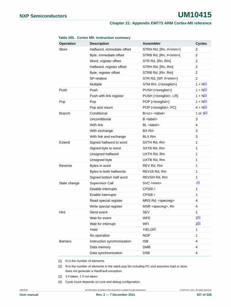
NXP Semiconductors UM10415Chapter 21: Appendix EM773 ARM Cortex-M0 reference
[1] N is the number of elements.
[2] N is the number of elements in the stack-pop list including PC and assumes load or store
does not generate a HardFault exception.
[3] 3 if taken, 1 if not taken.
[4] Cycle count depends on core and debug configuration.
Store Halfword, immediate offset STRH Rd, [Rn, #<imm>] 2
Byte, immediate offset STRB Rd, [Rn, #<imm>] 2
Word, register offset STR Rd, [Rn, Rm] 2
Halfword, register offset STRH Rd, [Rn, Rm] 2
Byte, register offset STRB Rd, [Rn, Rm] 2
SP-relative STR Rd, [SP, #<imm>] 2
Multiple STM Rn!, {<loreglist>} 1 + N[1]
Push Push PUSH {<loreglist>} 1 + N[1]
Push with link register PUSH {<loreglist>, LR} 1 + N[1]
Pop Pop POP {<loreglist>} 1 + N[1]
Pop and return POP {<loreglist>, PC} 4 + N[2]
Branch Conditional B<cc> <label> 1 or 3[3]
Unconditional B <label> 3
With link BL <label> 4
With exchange BX Rm 3
With link and exchange BLX Rm 3
Extend Signed halfword to word SXTH Rd, Rm 1
Signed byte to word SXTB Rd, Rm 1
Unsigned halfword UXTH Rd, Rm 1
Unsigned byte UXTB Rd, Rm 1
Reverse Bytes in word REV Rd, Rm 1
Bytes in both halfwords REV16 Rd, Rm 1
Signed bottom half word REVSH Rd, Rm 1
State change Supervisor Call SVC <imm> -[4]
Disable interrupts CPSID i 1
Enable interrupts CPSIE i 1
Read special register MRS Rd, <specreg> 4
Write special register MSR <specreg>, Rn 4
Hint Send event SEV 1
Wait for event WFE 2[5]
Wait for interrupt WFI 2[5]
Yield YIELD[6] 1
No operation NOP 1
Barriers Instruction synchronization ISB 4
Data memory DMB 4
Data synchronization DSB 4
Table 265. Cortex M0- instruction summary
Operation Description Assembler Cycles
UM10415 All information provided in this document is subject to legal disclaimers. © NXP B.V. 2011. All rights reserved.
User manual Rev. 2 — 7 December 2011 307 of 326
NXP Semiconductors UM10415Chapter 21: Appendix EM773 ARM Cortex-M0 reference
[5] Excludes time spend waiting for an interrupt or event.
[6] Executes as NOP.
UM10415 All information provided in this document is subject to legal disclaimers. © NXP B.V. 2011. All rights reserved.
User manual Rev. 2 — 7 December 2011 308 of 326
22.1 Abbreviations
22.2 References
[1] ARM DUI 0497A — Cortex-M0 Devices Generic User Guide
[2] ARM DDI 0432C — Cortex-M0 Revision r0p0 Technical Reference Manual
UM10415Chapter 22: Supplementary informationRev. 2 — 7 December 2011 User manual
Table 266. Abbreviations
Acronym Description
AHB Advanced High-performance Bus
AMBA Advanced Microcontroller Bus Architecture
APB Advanced Peripheral Bus
BOD BrownOut Detection
GPIO General Purpose Input/Output
PLL Phase-Locked Loop
SPI Serial Peripheral Interface
SSI Serial Synchronous Interface
TTL Transistor-Transistor Logic
UART Universal Asynchronous Receiver/Transmitter
UM10415 All information provided in this document is subject to legal disclaimers. © NXP B.V. 2011. All rights reserved.
User manual Rev. 2 — 7 December 2011 309 of 326
NXP Semiconductors UM10415Chapter 22: Supplementary information
22.3 Legal information
22.3.1 Definitions
Draft — The document is a draft version only. The content is still under internal review and subject to formal approval, which may result in modifications or additions. NXP Semiconductors does not give any representations or warranties as to the accuracy or completeness of information included herein and shall have no liability for the consequences of use of such information.
22.3.2 Disclaimers
Limited warranty and liability — Information in this document is believed to be accurate and reliable. However, NXP Semiconductors does not give any representations or warranties, expressed or implied, as to the accuracy or completeness of such information and shall have no liability for the consequences of use of such information.
In no event shall NXP Semiconductors be liable for any indirect, incidental, punitive, special or consequential damages (including - without limitation - lost profits, lost savings, business interruption, costs related to the removal or replacement of any products or rework charges) whether or not such damages are based on tort (including negligence), warranty, breach of contract or any other legal theory.
Notwithstanding any damages that customer might incur for any reason whatsoever, NXP Semiconductors’ aggregate and cumulative liability towards customer for the products described herein shall be limited in accordance with the Terms and conditions of commercial sale of NXP Semiconductors.
Right to make changes — NXP Semiconductors reserves the right to make changes to information published in this document, including without limitation specifications and product descriptions, at any time and without notice. This document supersedes and replaces all information supplied prior to the publication hereof.
Suitability for use — NXP Semiconductors products are not designed, authorized or warranted to be suitable for use in life support, life-critical or safety-critical systems or equipment, nor in applications where failure or malfunction of an NXP Semiconductors product can reasonably be expected
to result in personal injury, death or severe property or environmental damage. NXP Semiconductors accepts no liability for inclusion and/or use of NXP Semiconductors products in such equipment or applications and therefore such inclusion and/or use is at the customer’s own risk.
Applications — Applications that are described herein for any of these products are for illustrative purposes only. NXP Semiconductors makes no representation or warranty that such applications will be suitable for the specified use without further testing or modification.
Customers are responsible for the design and operation of their applications and products using NXP Semiconductors products, and NXP Semiconductors accepts no liability for any assistance with applications or customer product design. It is customer’s sole responsibility to determine whether the NXP Semiconductors product is suitable and fit for the customer’s applications and products planned, as well as for the planned application and use of customer’s third party customer(s). Customers should provide appropriate design and operating safeguards to minimize the risks associated with their applications and products.
NXP Semiconductors does not accept any liability related to any default, damage, costs or problem which is based on any weakness or default in the customer’s applications or products, or the application or use by customer’s third party customer(s). Customer is responsible for doing all necessary testing for the customer’s applications and products using NXP Semiconductors products in order to avoid a default of the applications and the products or of the application or use by customer’s third party customer(s). NXP does not accept any liability in this respect.
Export control — This document as well as the item(s) described herein may be subject to export control regulations. Export might require a prior authorization from competent authorities.
22.3.3 TrademarksNotice: All referenced brands, product names, service names and trademarks are the property of their respective owners.
I2C-bus — logo is a trademark of NXP B.V.
UM10415 All information provided in this document is subject to legal disclaimers. © NXP B.V. 2011. All rights reserved.
User manual Rev. 2 — 7 December 2011 310 of 326
NXP Semiconductors UM10415Chapter 22: Supplementary information
22.4 Tables
Table 1. Ordering information . . . . . . . . . . . . . . . . . . . . .4Table 2. Pin summary. . . . . . . . . . . . . . . . . . . . . . . . . . . .9Table 3. Register overview: system control block (base
address 0x4004 8000) . . . . . . . . . . . . . . . . . .10Table 4. System memory remap register
(SYSMEMREMAP, address 0x4004 8000) bit description . . . . . . . . . . . . . . . . . . . . . . . . . . . .12
Table 5. Peripheral reset control register (PRESETCTRL, address 0x4004 8004) bit description. . . . . . . .12
Table 6. System PLL control register (SYSPLLCTRL, address 0x4004 8008) bit description . . . . . . .13
Table 7. System PLL status register (SYSPLLSTAT, address 0x4004 800C) bit description . . . . . . .13
Table 8. System oscillator control register (SYSOSCCTRL, address 0x4004 8020) bit description. . . . . . . .13
Table 9. Watchdog oscillator control register (WDTOSCCTRL, address 0x4004 8024) bit description . . . . . . . . . . . . . . . . . . . . . . . . . . . .14
Table 10. Internal resonant crystal control register (IRCCTRL, address 0x4004 8028) bit description15
Table 11. System reset status register (SYSRSTSTAT, address 0x4004 8030) bit description. . . . . . . .16
Table 12. System PLL clock source select register (SYSPLLCLKSEL, address 0x4004 8040) bit description . . . . . . . . . . . . . . . . . . . . . . . . . . . .16
Table 13. System PLL clock source update enable register (SYSPLLUEN, address 0x4004 8044) bit description . . . . . . . . . . . . . . . . . . . . . . . . . . . .17
Table 14. Main clock source select register (MAINCLKSEL, address 0x4004 8070) bit description. . . . . . . .17
Table 15. Main clock source update enable register (MAINCLKUEN, address 0x4004 8074) bit description . . . . . . . . . . . . . . . . . . . . . . . . . . . .18
Table 16. System AHB clock divider register (SYSAHBCLKDIV, address 0x4004 8078) bit description . . . . . . . . . . . . . . . . . . . . . . . . . . . .18
Table 17. System AHB clock control register (SYSAHBCLKCTRL, address 0x4004 8080) bit description . . . . . . . . . . . . . . . . . . . . . . . . . . .18
Table 18. SPI0 clock divider register (SSP0CLKDIV, address 0x4004 8094) bit description. . . . . . . .20
Table 19. UART clock divider register (UARTCLKDIV, address 0x4004 8098) bit description. . . . . . . .20
Table 20. WDT clock source select register (WDTCLKSEL, address 0x4004 80D0) bit description . . . . . . .21
Table 21. WDT clock source update enable register (WDTCLKUEN, address 0x4004 80D4) bit description . . . . . . . . . . . . . . . . . . . . . . . . . . . .21
Table 22. WDT clock divider register (WDTCLKDIV, address 0x4004 80D8) bit description . . . . . . . . . . . . . .21
Table 23. CLKOUT clock source select register (CLKOUTCLKSEL, address 0x4004 80E0) bit description . . . . . . . . . . . . . . . . . . . . . . . . . . . .22
Table 24. CLKOUT clock source update enable register (CLKOUTUEN, address 0x4004 80E4) bit
description . . . . . . . . . . . . . . . . . . . . . . . . . . . . 22Table 25. CLKOUT clock divider registers
(CLKOUTCLKDIV, address 0x4004 80E8) bit description . . . . . . . . . . . . . . . . . . . . . . . . . . . . 22
Table 26. POR captured PIO status registers 0 (PIOPORCAP0, address 0x4004 8100) bit description . . . . . . . . . . . . . . . . . . . . . . . . . . . . 23
Table 27. POR captured PIO status registers 1 (PIOPORCAP1, address 0x4004 8104) bit description . . . . . . . . . . . . . . . . . . . . . . . . . . . . 23
Table 28. BOD control register (BODCTRL, address 0x4004 8150) bit description. . . . . . . . . . . . . . . . . . . . . 23
Table 29. System tick timer calibration register (SYSTCKCAL, address 0x4004 8158) bit description . . . . . . . . . . . . . . . . . . . . . . . . . . . . 24
Table 30. Start logic edge control register 0 (STARTAPRP0, address 0x4004 8200) bit description . . . . . . 24
Table 31. Start logic signal enable register 0 (STARTERP0, address 0x4004 8204) bit description . . . . . . 25
Table 32. Start logic reset register 0 (STARTRSRP0CLR, address 0x4004 8208) bit description . . . . . . 25
Table 33. Start logic status register 0 (STARTSRP0, address 0x4004 820C) bit description . . . . . . 25
Table 34. Allowed values for PDSLEEPCFG register . . . 26Table 35. Deep-sleep configuration register
(PDSLEEPCFG, address 0x4004 8230) bit description . . . . . . . . . . . . . . . . . . . . . . . . . . . 27
Table 36. Wake-up configuration register (PDAWAKECFG, address 0x4004 8234) bit description . . . . . . 27
Table 37. Power-down configuration register (PDRUNCFG, address 0x4004 8238) bit description . . . . . . 28
Table 38. Device ID register (DEVICE_ID, address 0x4004 83F4) bit description . . . . . . . . . . . . . . . . . . . . 29
Table 39. PLL frequency parameters. . . . . . . . . . . . . . . . 38Table 40. PLL configuration examples. . . . . . . . . . . . . . . 39Table 41. Flash configuration register (FLASHCFG, address
0x4003 C010) bit description . . . . . . . . . . . . . . 39Table 42. Register overview: PMU (base address 0x4003
8000) . . . . . . . . . . . . . . . . . . . . . . . . . . . . . . . 40Table 43. Power control register (PCON, address 0x4003
8000) bit description . . . . . . . . . . . . . . . . . . . . 40Table 44. General purpose registers 0 to 3 (GPREG0 -
GPREG3, address 0x4003 8004 to 0x4003 8010) bit description . . . . . . . . . . . . . . . . . . . . . . . . . 41
Table 45. General purpose register 4 (GPREG4, address 0x4003 8014) bit description . . . . . . . . . . . . . 41
Table 46. Connection of interrupt sources to the Vectored Interrupt Controller . . . . . . . . . . . . . . . . . . . . . 42
Table 47. Register overview: I/O configuration (base address 0x4004 4000) . . . . . . . . . . . . . . . . . . . 46
Table 48. I/O configuration registers ordered by port number47
Table 49. IOCON_PIO2_0 register (IOCON_PIO2_0, address 0x4004 4008) bit description . . . . . . . 48
Table 50. IOCON_nRESET_PIO0_0 register (IOCON_nRESET_PIO0_0, address 0x4004
UM10415 All information provided in this document is subject to legal disclaimers. © NXP B.V. 2011. All rights reserved.
User manual Rev. 2 — 7 December 2011 311 of 326

NXP Semiconductors UM10415Chapter 22: Supplementary information
400C) bit description. . . . . . . . . . . . . . . . . . . . .48Table 51. IOCON_PIO0_1 register (IOCON_PIO0_1,
address 0x4004 4010) bit description . . . . . . .49Table 52. IOCON_PIO1_8 register (IOCON_PIO1_8,
address 0x4004 4014) bit description . . . . . . .49Table 53. IOCON_PIO0_2 register (IOCON_PIO0_2,
address 0x4004 401C) bit description . . . . . . .50Table 54. IOCON_PIO0_3 register (IOCON_PIO0_3
address 0x4004 402C) bit description . . . . . . .51Table 55. IOCON_PIO0_4 register (IOCON_PIO0_4
address 0x4004 4030) bit description . . . . . . .51Table 56. IOCON_PIO0_5 register (IOCON_PIO0_5
address 0x4004 4034) bit description . . . . . . .52Table 57. IOCON_PIO1_9 register (IOCON_PIO1_9
address 0x4004 4038) bit description . . . . . . .53Table 58. IOCON_PIO3_4 register (IOCON_PIO3_4,
address 0x4004 403C) bit description . . . . . . .53Table 59. IOCON_PIO3_5 register (IOCON_PIO3_5,
address 0x4004 4048) bit description . . . . . . .54Table 60. IOCON_PIO0_6 register (IOCON_PIO0_6
address 0x4004 404C) bit description . . . . . . .54Table 61. IOCON_PIO0_7 register (IOCON_PIO0_7,
address 0x4004 4050) bit description. . . . . . . .55Table 62. IOCON_PIO0_8 register (IOCON_PIO0_8,
address 0x4004 4060) bit description . . . . . . .55Table 63. IOCON_PIO0_9 register (IOCON_PIO0_9,
address 0x4004 4064) bit description . . . . . . .56Table 64. IOCON_SWCLK_PIO0_10 register
(IOCON_SWCLK_PIO0_10, address 0x4004 4068) bit description . . . . . . . . . . . . . . . . . . . .57
Table 65. IOCON_R_PIO1_1 register (IOCON_R_PIO1_1, address 0x4004 407C) bit description . . . . . . .58
Table 66. IOCON_R_PIO1_2 register (IOCON_R_PIO1_2, address 0x4004 4080) bit description . . . . . . .59
Table 67. IOCON_SWDIO_PIO1_3 register (IOCON_SWDIO_PIO1_3, address 0x4004 4090) bit description . . . . . . . . . . . . . . . . . . . . . . . . .59
Table 68. IOCON_PIO1_4 register (IOCON_PIO1_4, address 0x4004 4094) bit description . . . . . . .60
Table 69. IOCON_PIO1_11 register (IOCON_PIO1_11 address 0x4004 4098) bit description . . . . . . .61
Table 70. IOCON_PIO3_2 register (IOCON_PIO3_2, address 0x4004 409C) bit description . . . . . .61
Table 71. IOCON_PIO1_5 register (IOCON_PIO1_5, address 0x4004 40A0) bit description . . . . . . .62
Table 72. IOCON_PIO1_6 register (IOCON_PIO1_6, address 0x4004 40A4) bit description . . . . . . .62
Table 73. IOCON_PIO1_7 register (IOCON_PIO1_7, address 0x4004 40A8) bit description . . . . . . .63
Table 74. IOCON SCK location register (IOCON_SCK_LOC, address 0x4004 40B0) bit description . . . . . . . . . . . . . . . . . . . . . . . . . . . .64
Table 75. EM773 pin configurations . . . . . . . . . . . . . . . . .65Table 76. UM10415 pin description table (HVQFN33
package) . . . . . . . . . . . . . . . . . . . . . . . . . . . . .66Table 77. GPIO configuration . . . . . . . . . . . . . . . . . . . . . .69Table 78. Register overview: GPIO (base address port 0:
0x5000 0000; port 1: 0x5001 0000, port 2: 0x5002
0000; port 3: 0x5003 0000) . . . . . . . . . . . . . . . 69Table 79. GPIOnDATA register (GPIO0DATA, address
0x5000 0000 to 0x5000 3FFC; GPIO1DATA, address 0x5001 0000 to 0x5001 3FFC; GPIO2DATA, address 0x5002 0000 to 0x5002 3FFC; GPIO3DATA, address 0x5003 0000 to 0x5003 3FFC) bit description . . . . . . . . . . . . . 70
Table 80. GPIOnDIR register (GPIO0DIR, address 0x5000 8000 to GPIO3DIR, address 0x5003 8000) bit description . . . . . . . . . . . . . . . . . . . . . . . . . . . . 71
Table 81. GPIOnIS register (GPIO0IS, address 0x5000 8004 to GPIO3IS, address 0x5003 8004) bit description . . . . . . . . . . . . . . . . . . . . . . . . . . . . 71
Table 82. GPIOnIBE register (GPIO0IBE, address 0x5000 8008 to GPIO3IBE, address 0x5003 8008) bit description . . . . . . . . . . . . . . . . . . . . . . . . . . . . 71
Table 83. GPIOnIEV register (GPIO0IEV, address 0x5000 800C to GPIO3IEV, address 0x5003 800C) bit description . . . . . . . . . . . . . . . . . . . . . . . . . . . . 72
Table 84. GPIOnIE register (GPIO0IE, address 0x5000 8010 to GPIO3IE, address 0x5003 8010) bit description . . . . . . . . . . . . . . . . . . . . . . . . . . . . 72
Table 85. GPIOnIRS register (GPIO0IRS, address 0x5000 8014 to GPIO3IRS, address 0x5003 8014) bit description . . . . . . . . . . . . . . . . . . . . . . . . . . . . 72
Table 86. GPIOnMIS register (GPIO0MIS, address 0x5000 8018 to GPIO3MIS, address 0x5003 8018) bit description . . . . . . . . . . . . . . . . . . . . . . . . . . . . 73
Table 87. GPIOnIC register (GPIO0IC, address 0x5000 801C to GPIO3IC, address 0x5003 801C) bit description . . . . . . . . . . . . . . . . . . . . . . . . . . . . 73
Table 88. UART pin description . . . . . . . . . . . . . . . . . . . . 76Table 89. Register overview: UART (base address: 0x4000
8000) . . . . . . . . . . . . . . . . . . . . . . . . . . . . . . . . 77Table 90. UART Receiver Buffer Register (U0RBR -
address 0x4000 8000 when DLAB = 0, Read Only) bit description . . . . . . . . . . . . . . . . . . . . 79
Table 91. UART Transmitter Holding Register (U0THR - address 0x4000 8000 when DLAB = 0, Write Only) bit description . . . . . . . . . . . . . . . . . . . . . 79
Table 92. UART Divisor Latch LSB Register (U0DLL - address 0x4000 8000 when DLAB = 1) bit description . . . . . . . . . . . . . . . . . . . . . . . . . . . . 80
Table 93. UART Divisor Latch MSB Register (U0DLM - address 0x4000 8004 when DLAB = 1) bit description . . . . . . . . . . . . . . . . . . . . . . . . . . . . 80
Table 94. UART Interrupt Enable Register (U0IER - address 0x4000 8004 when DLAB = 0) bit description 80
Table 95. UART Interrupt Identification Register (U0IIR - address 0x4004 8008, Read Only) bit description 81
Table 96. UART Interrupt Handling . . . . . . . . . . . . . . . . . 82Table 97. UART FIFO Control Register (U0FCR - address
0x4000 8008, Write Only) bit description . . . . . 83Table 98. UART Line Control Register (U0LCR - address
0x4000 800C) bit description . . . . . . . . . . . . . 83Table 99. UART0 Modem Control Register (U0MCR -
address 0x4000 8010) bit description . . . . . . . 84
UM10415 All information provided in this document is subject to legal disclaimers. © NXP B.V. 2011. All rights reserved.
User manual Rev. 2 — 7 December 2011 312 of 326

NXP Semiconductors UM10415Chapter 22: Supplementary information
Table 100. Modem status interrupt generation . . . . . . . . .86Table 101. UART Line Status Register (U0LSR - address
0x4000 8014, Read Only) bit description . . . .87Table 102. UART Modem Status Register (U0MSR - address
0x4000 8018) bit description . . . . . . . . . . . . . .89Table 103. UART Scratch Pad Register (U0SCR - address
0x4000 8014) bit description . . . . . . . . . . . . . .89Table 104. Auto-baud Control Register (U0ACR - address
0x4000 8020) bit description . . . . . . . . . . . . . .90Table 105. UART Fractional Divider Register (U0FDR -
address 0x4000 8028) bit description. . . . . . . .93Table 106. Fractional Divider setting look-up table . . . . . .95Table 107. UART Transmit Enable Register (U0TER -
address 0x4000 8030) bit description. . . . . . . .96Table 108. UART RS485 Control register (U0RS485CTRL -
address 0x4000 804C) bit description . . . . . .96Table 109. UART RS-485 Address Match register
(U0RS485ADRMATCH - address 0x4000 8050) bit description . . . . . . . . . . . . . . . . . . . . . . . . . .97
Table 110. UART RS-485 Delay value register (U0RS485DLY - address 0x4000 8054) bit description . . . . . . . . . . . . . . . . . . . . . . . . . . . .97
Table 111. I2C-bus pin description . . . . . . . . . . . . . . . . . .103Table 112. Register overview: I2C (base address 0x4000
0000) . . . . . . . . . . . . . . . . . . . . . . . . . . . . . .103Table 113. I2C Control Set register (I2C0CONSET - address
0x4000 0000) bit description . . . . . . . . . . . . .104Table 114. I2C Status register (I2C0STAT - 0x4000 0004) bit
description . . . . . . . . . . . . . . . . . . . . . . . . . . .106Table 115. I2C Data register (I2C0DAT - 0x4000 0008) bit
description . . . . . . . . . . . . . . . . . . . . . . . . . . .106Table 116. I2C Slave Address register 0 (I2C0ADR0-
0x4000 000C) bit description . . . . . . . . . . . . .107Table 117. I2C SCL HIGH Duty Cycle register (I2C0SCLH -
address 0x4000 0010) bit description. . . . . . .107Table 118. I2C SCL Low duty cycle register (I2C0SCLL -
0x4000 0014) bit description . . . . . . . . . . . . .107Table 119. I2SCLL + I2SCLH values for selected I2C clock
values . . . . . . . . . . . . . . . . . . . . . . . . . . . . . . .108Table 120. I2C Control Clear register (I2C0CONCLR -
0x4000 0018) bit description . . . . . . . . . . . . .108Table 121. I2C Monitor mode control register (I2C0MMCTRL
- 0x4000 001C) bit description . . . . . . . . . . . .109Table 122. I2C Slave Address registers (I2C0ADR[1, 2, 3]-
0x4000 00[20, 24, 28]) bit description . . . . . . 110Table 123. I2C Data buffer register (I2C0DATA_BUFFER -
0x4000 002C) bit description . . . . . . . . . . . . . 111Table 124. I2C Mask registers (I2C0MASK[0, 1, 2, 3] -
0x4000 00[30, 34, 38, 3C]) bit description . . . 111Table 125. I2C0CONSET and I2C1CONSET used to
configure Master mode. . . . . . . . . . . . . . . . . . 112Table 126. I2C0CONSET and I2C1CONSET used to
configure Slave mode. . . . . . . . . . . . . . . . . . . 113Table 127. Abbreviations used to describe an I2C operation.
119Table 128. I2CONSET used to initialize Master Transmitter
mode. . . . . . . . . . . . . . . . . . . . . . . . . . . . . . . . 119Table 129. Master Transmitter mode. . . . . . . . . . . . . . . .121
Table 130. Master Receiver mode . . . . . . . . . . . . . . . . . 124Table 131. I2C0ADR and I2C1ADR usage in Slave Receiver
mode . . . . . . . . . . . . . . . . . . . . . . . . . . . . . . . 126Table 132. I2C0CONSET and I2C1CONSET used to
initialize Slave Receiver mode . . . . . . . . . . . . 126Table 133. Slave Receiver mode . . . . . . . . . . . . . . . . . 127Table 134. Slave Transmitter mode . . . . . . . . . . . . . . . . 131Table 135. Miscellaneous States . . . . . . . . . . . . . . . . . . 133Table 136. SPI pin descriptions . . . . . . . . . . . . . . . . . . . 145Table 137. Register overview: SPI0 (base address 0x4004
0000) . . . . . . . . . . . . . . . . . . . . . . . . . . . . . . . 146Table 138: SPI/SSP Control Register 0 (SSP0CR0 - address
0x4004 0000) bit description . . . . . . . . . . . . . 147Table 139: SPI/SSP Control Register 1 (SSP0CR1 - address
0x4004 0004) bit description . . . . . . . . . . . . . 148Table 140: SPI/SSP Data Register (SSP0DR - address
0x4004 0008) bit description . . . . . . . . . . . . . 149Table 141: SPI/SSP Status Register (SSP0SR - address
0x4004 000C) bit description . . . . . . . . . . . . . 149Table 142: SPI/SSP Clock Prescale Register (SSP0CPSR -
address 0x4004 0010) bit description . . . . . . 150Table 143: SPI/SSP Interrupt Mask Set/Clear register
(SSP0IMSC - address 0x4004 0014) bit description . . . . . . . . . . . . . . . . . . . . . . . . . . . 150
Table 144: SPI/SSP Raw Interrupt Status register (SSP0RIS - address 0x4004 0018) bit description . . . . . 151
Table 145: SPI/SSP Masked Interrupt Status register (SSP0MIS - address 0x4004 001C) bit description151
Table 146: SPI/SSP interrupt Clear Register (SSP0ICR - address 0x4004 0020) bit description . . . . . . 152
Table 147. Counter/timer pin description . . . . . . . . . . . . 160Table 148. Register overview: 16-bit counter/timer 0 CT16B0
(base address 0x4000 C000) . . . . . . . . . . . . 161Table 149. Interrupt Register (TMR16B0IR - address
0x4000 C000) bit description . . . . . . . . . . . . . 162Table 150. Timer Control Register (TMR16B0TCR - address
0x4000 C004) bit description . . . . . . . . . . . . 162Table 151. Match Control Register (TMR16B0MCR -
address 0x4000 C014) bit description . . . . 163Table 152. Capture Control Register (TMR16B0CCR -
address 0x4000 C028) bit description . . . . . 164Table 153. External Match Register (TMR16B0EMR -
address 0x4000 C03C) bit description . . . . . 165Table 154. External match control . . . . . . . . . . . . . . . . . 165Table 155. Count Control Register (TMR16B0CTCR -
address 0x4000 C070) bit description . . . . . 166Table 156. PWM Control Register (TMR16B0PWMC -
address 0x4000 C074 and TMR16B1PWMC- address 0x4001 0074) bit description . . . . . . 167
Table 157. Counter/timer pin description . . . . . . . . . . . . 171Table 158. Register overview: 32-bit counter/timer 0 CT32B0
(base address 0x4001 4000) . . . . . . . . . . . . 172Table 159. Register overview: 32-bit counter/timer 1 CT32B1
(base address 0x4001 8000) . . . . . . . . . . . . 173Table 160: Interrupt Register (TMR32B0IR - address
0x4001 4000 and TMR32B1IR - address 0x4001 8000) bit description . . . . . . . . . . . . . 173
UM10415 All information provided in this document is subject to legal disclaimers. © NXP B.V. 2011. All rights reserved.
User manual Rev. 2 — 7 December 2011 313 of 326

NXP Semiconductors UM10415Chapter 22: Supplementary information
Table 161: Timer Control Register (TMR32B0TCR - address 0x4001 4004 and TMR32B1TCR - address 0x4001 8004) bit description . . . . . . . . . . . . .174
Table 162: Match Control Register (TMR32B0MCR - address 0x4001 4014 and TMR32B1MCR - address 0x4001 8014) bit description. . . . . . .175
Table 163: Capture Control Register (TMR32B0CCR - address 0x4001 4028) bit description. . . . . . .176
Table 164: External Match Register (TMR32B0EMR - address 0x4001 403C and TMR32B1EMR - address0x4001 803C) bit description . . . . . . .177
Table 165. External match control . . . . . . . . . . . . . . . . . .177Table 166: Count Control Register (TMR32B0CTCR -
address 0x4001 4070 and TMR32B1TCR - address 0x4001 8070) bit description . . . . . .178
Table 167: PWM Control Register (TMR32B0PWMC - 0x4001 4074 and TMR32B1PWMC - 0x4001 8074) bit description . . . . . . . . . . . . . . . . . . . .179
Table 168. Register overview: Watchdog timer (base address 0x4000 4000) . . . . . . . . . . . . . . . . . .185
Table 169: Watchdog Mode register (WDMOD - 0x4000 4000) bit description . . . . . . . . . . . . .185
Table 170. Watchdog operating modes selection . . . . . .186Table 171: Watchdog Timer Constant register (WDTC -
0x4000 4004) bit description . . . . . . . . . . . . .187Table 172: Watchdog Feed register (WDFEED -
0x4000 4008) bit description . . . . . . . . . . . . .187Table 173: Watchdog Timer Value register (WDTV -
0x4000 400C) bit description . . . . . . . . . . . . .187Table 174: Watchdog Timer Warning Interrupt register
(WDWARNINT - 0x4000 4014) bit description188Table 175: Watchdog Timer Window register (WDWINDOW
- 0x4000 4018) bit description . . . . . . . . . . . .188Table 176. set_pll routine . . . . . . . . . . . . . . . . . . . . . . . .191Table 177. set_power routine . . . . . . . . . . . . . . . . . . . . .196Table 178. Register overview: SysTick timer (base address
0xE000 E000). . . . . . . . . . . . . . . . . . . . . . . . .199Table 179. SysTick Timer Control and status register
(SYST_CSR - 0xE000 E010) bit description .200Table 180. System Timer Reload value register (SYST_RVR
- 0xE000 E014) bit description . . . . . . . . . . . .200Table 181. System Timer Current value register (SYST_CVR
- 0xE000 E018) bit description . . . . . . . . . . . .200Table 182. System Timer Calibration value register
(SYST_CALIB - 0xE000 E01C) bit description. . .201
Table 183. Serial Wire Debug pin description . . . . . . . . .203Table 184. Metrology Engine configuration parameters .207Table 185. Metrology result class structure . . . . . . . . . . .215Table 186. Flash sector configuration . . . . . . . . . . . . . . .219Table 187. Code Read Protection options. . . . . . . . . . . .220Table 188. Code Read Protection hardware/software
interaction . . . . . . . . . . . . . . . . . . . . . . . . . . .220Table 189. ISP commands allowed for different CRP levels .
221Table 190. UART ISP command summary . . . . . . . . . . .223Table 191. UART ISP Unlock command . . . . . . . . . . . . .224Table 192. UART ISP Set Baud Rate command . . . . . . .224
Table 193. UART ISP Echo command . . . . . . . . . . . . . . 224Table 194. UART ISP Write to RAM command. . . . . . . . 225Table 195. UART ISP Read Memory command . . . . . . . 225Table 196. UART ISP Prepare sector(s) for write operation
command . . . . . . . . . . . . . . . . . . . . . . . . . . . . 226Table 197. UART ISP Copy command . . . . . . . . . . . . . . 226Table 198. UART ISP Go command . . . . . . . . . . . . . . . . 227Table 199. UART ISP Erase sector command . . . . . . . . 227Table 200. UART ISP Blank check sector command . . . 228Table 201. UART ISP Read Part Identification command228Table 202. EM773 part identification numbers . . . . . . . . 228Table 203. UART ISP Read Boot Code version number
command . . . . . . . . . . . . . . . . . . . . . . . . . . . . 228Table 204. UART ISP Compare command . . . . . . . . . . . 229Table 205. UART ISP ReadUID command . . . . . . . . . . . 229Table 206. UART ISP Return Codes Summary . . . . . . . 229Table 207. IAP Command Summary . . . . . . . . . . . . . . . 231Table 208. IAP Prepare sector(s) for write operation
command . . . . . . . . . . . . . . . . . . . . . . . . . . . . 232Table 209. IAP Copy RAM to flash command. . . . . . . . . 233Table 210. IAP Erase Sector(s) command . . . . . . . . . . . 233Table 211. IAP Blank check sector(s) command. . . . . . . 234Table 212. IAP Read Part Identification command . . . . . 234Table 213. IAP Read Boot Code version number command
234Table 214. IAP Compare command . . . . . . . . . . . . . . . . 235Table 215. IAP Reinvoke ISP . . . . . . . . . . . . . . . . . . . . . 235Table 216. IAP ReadUID command . . . . . . . . . . . . . . . . 235Table 217. IAP Status Codes Summary . . . . . . . . . . . . . 236Table 218. Memory mapping in debug mode . . . . . . . . . 236Table 219. Flash configuration register (FLASHCFG,
address 0x4003 C010) bit description . . . . . . 237Table 220. Serial Wire Debug pin description. . . . . . . . . 238Table 221. Summary of processor mode and stack use
options . . . . . . . . . . . . . . . . . . . . . . . . . . . . . . 242Table 222. Core register set summary . . . . . . . . . . . . . . 243Table 223. PSR register combinations . . . . . . . . . . . . . . 244Table 224. APSR bit assignments . . . . . . . . . . . . . . . . . 245Table 225. IPSR bit assignments . . . . . . . . . . . . . . . . . . 245Table 226. EPSR bit assignments . . . . . . . . . . . . . . . . . 246Table 227. PRIMASK register bit assignments . . . . . . . . 246Table 228. CONTROL register bit assignments . . . . . . . 247Table 229. Memory access behavior . . . . . . . . . . . . . . . 251Table 230. Properties of different exception types . . . . . 253Table 231. Exception return behavior . . . . . . . . . . . . . . . 258Table 232. Cortex-M0 instructions . . . . . . . . . . . . . . . . . 261Table 233. CMSIS intrinsic functions to generate some
Cortex-M0 instructions . . . . . . . . . . . . . . . . . . 262Table 234. insic functions to access the special registers . .
263Table 235. Condition code suffixes . . . . . . . . . . . . . . . . . 268Table 236. Access instructions . . . . . . . . . . . . . . . . . . . 268Table 237. Data processing instructions . . . . . . . . . . . . . 274Table 238. ADC, ADD, RSB, SBC and SUB operand
restrictions . . . . . . . . . . . . . . . . . . . . . . . . . . . 276Table 239. Branch and control instructions. . . . . . . . . . . 283Table 240. Branch ranges. . . . . . . . . . . . . . . . . . . . . . . . 284Table 241. Miscellaneous instructions . . . . . . . . . . . . . . 285
UM10415 All information provided in this document is subject to legal disclaimers. © NXP B.V. 2011. All rights reserved.
User manual Rev. 2 — 7 December 2011 314 of 326

NXP Semiconductors UM10415Chapter 22: Supplementary information
Table 242. Core peripheral register regions . . . . . . . . . .292Table 243. NVIC register summary . . . . . . . . . . . . . . . . .293Table 244. CMISIS access NVIC functions . . . . . . . . . .293Table 245. ISER bit assignments. . . . . . . . . . . . . . . . . . .294Table 246. ICER bit assignments . . . . . . . . . . . . . . . . . .294Table 247. ISPR bit assignments. . . . . . . . . . . . . . . . . . .294Table 248. ICPR bit assignments . . . . . . . . . . . . . . . . . .295Table 249. IPR bit assignments . . . . . . . . . . . . . . . . . . . .295Table 250. CMSIS functions for NVIC control . . . . . . . . .297Table 251. Summary of the SCB registers . . . . . . . . . . .298Table 252. CPUID register bit assignments. . . . . . . . . . .298Table 253. ICSR bit assignments . . . . . . . . . . . . . . . . . .299Table 254. AIRCR bit assignments . . . . . . . . . . . . . . . . .301Table 255. SCR bit assignments . . . . . . . . . . . . . . . . . . .301Table 256. CCR bit assignments . . . . . . . . . . . . . . . . . . .302Table 257. System fault handler priority fields . . . . . . . . .302Table 258. SHPR2 register bit assignments . . . . . . . . . .303Table 259. SHPR3 register bit assignments . . . . . . . . . .303Table 260. System timer registers summary . . . . . . . . . .303Table 261. SYST_CSR bit assignments . . . . . . . . . . . . .304Table 262. SYST_RVR bit assignments . . . . . . . . . . . . .304Table 263. SYST_CVR bit assignments . . . . . . . . . . . . .305Table 264. SYST_CALIB register bit assignments . . . . .305Table 265. Cortex M0- instruction summary . . . . . . . . . .305Table 266. Abbreviations . . . . . . . . . . . . . . . . . . . . . . . .309
UM10415 All information provided in this document is subject to legal disclaimers. © NXP B.V. 2011. All rights reserved.
User manual Rev. 2 — 7 December 2011 315 of 326

NXP Semiconductors UM10415Chapter 22: Supplementary information
22.5 Figures
Fig 1. EM773 block diagram . . . . . . . . . . . . . . . . . . . . . .5Fig 2. EM773 memory map . . . . . . . . . . . . . . . . . . . . . . .8Fig 3. EM773 CGU block diagram . . . . . . . . . . . . . . . . .10Fig 4. Start-up timing . . . . . . . . . . . . . . . . . . . . . . . . . . .31Fig 5. System PLL block diagram . . . . . . . . . . . . . . . . .37Fig 6. Standard I/O pin configuration . . . . . . . . . . . . . . .44Fig 7. Pin configuration HVQFN 33 package. . . . . . . . .65Fig 8. Masked write operation to the GPIODATA register .
74Fig 9. Masked read operation . . . . . . . . . . . . . . . . . . . .75Fig 10. Auto-RTS Functional Timing . . . . . . . . . . . . . . . .86Fig 11. Auto-CTS Functional Timing . . . . . . . . . . . . . . . .87Fig 12. Auto-baud a) mode 0 and b) mode 1 waveform .92Fig 13. Algorithm for setting UART dividers. . . . . . . . . . .94Fig 14. UART block diagram . . . . . . . . . . . . . . . . . . . . .100Fig 15. I2C-bus configuration . . . . . . . . . . . . . . . . . . . . .102Fig 16. Format in the Master Transmitter mode. . . . . . . 112Fig 17. Format of Master Receiver mode . . . . . . . . . . . 113Fig 18. A Master Receiver switches to Master Transmitter
after sending Repeated START . . . . . . . . . . . . . 113Fig 19. Format of Slave Receiver mode . . . . . . . . . . . . 114Fig 20. Format of Slave Transmitter mode . . . . . . . . . . 114Fig 21. I2C serial interface block diagram . . . . . . . . . . . 115Fig 22. Arbitration procedure . . . . . . . . . . . . . . . . . . . . . 117Fig 23. Serial clock synchronization. . . . . . . . . . . . . . . . 117Fig 24. Format and states in the Master Transmitter mode .
122Fig 25. Format and states in the Master Receiver mode. . .
125Fig 26. Format and states in the Slave Receiver mode.129Fig 27. Format and states in the Slave Transmitter mode . .
132Fig 28. Simultaneous Repeated START conditions from two
masters . . . . . . . . . . . . . . . . . . . . . . . . . . . . . . .134Fig 29. Forced access to a busy I2C-bus . . . . . . . . . . .134Fig 30. Recovering from a bus obstruction caused by a
LOW level on SDA. . . . . . . . . . . . . . . . . . . . . . .135Fig 31. Texas Instruments Synchronous Serial Frame
Format: a) Single and b) Continuous/back-to-back Two Frames Transfer. . . . . . . . . . . . . . . . . . . . .152
Fig 32. SPI frame format with CPOL=0 and CPHA=0 (a) Single and b) Continuous Transfer) . . . . . . . . . .153
Fig 33. SPI frame format with CPOL=0 and CPHA=1 . .154Fig 34. SPI frame format with CPOL = 1 and CPHA = 0 (a)
Single and b) Continuous Transfer) . . . . . . . . . .155Fig 35. SPI Frame Format with CPOL = 1 and CPHA = 1. .
156Fig 36. Microwire frame format (single transfer) . . . . . .157Fig 37. Microwire frame format (continuos transfers) . .157Fig 38. Microwire frame format setup and hold details .158Fig 39. Sample PWM waveforms with a PWM cycle length
of 100 (selected by MR3) and MAT3:0 enabled as PWM outputs by the PWCON register. . . . . . . .168
Fig 40. A timer cycle in which PR=2, MRx=6, and both interrupt and reset on match are enabled . . . . .168
Fig 41. A timer cycle in which PR=2, MRx=6, and both
interrupt and stop on match are enabled . . . . . 168Fig 42. 16-bit counter/timer block diagram . . . . . . . . . . 169Fig 43. Sample PWM waveforms with a PWM cycle length
of 100 (selected by MR3) and MAT3:0 enabled as PWM outputs by the PWCON register. . . . . . . . 180
Fig 44. A timer cycle in which PR=2, MRx=6, and both interrupt and reset on match are enabled . . . . . 180
Fig 45. A timer cycle in which PR=2, MRx=6, and both interrupt and stop on match are enabled . . . . . 180
Fig 46. 32-bit counter/timer block diagram . . . . . . . . . . 181Fig 47. Windowed Watchdog Timer (WWDT) block diagram
184Fig 48. Early Watchdog Feed with Windowed Mode
Enabled . . . . . . . . . . . . . . . . . . . . . . . . . . . . . . . 188Fig 49. Correct Watchdog Feed with Windowed Mode
Enabled . . . . . . . . . . . . . . . . . . . . . . . . . . . . . . . 189Fig 50. Watchdog Warning Interrupt . . . . . . . . . . . . . . . 189Fig 51. Power profiles pointer structure . . . . . . . . . . . . 190Fig 52. Power profiles usage. . . . . . . . . . . . . . . . . . . . . 195Fig 53. EM773 clock configuration for power API use . 195Fig 54. System tick timer block diagram . . . . . . . . . . . . 198Fig 55. EM773 with external measurement circuitry
connected to Metrology Engine. . . . . . . . . . . . . 202Fig 56. EM773 calibration measurements setup. . . . . . 209Fig 57. Boot process flowchart . . . . . . . . . . . . . . . . . . . 218Fig 58. IAP parameter passing . . . . . . . . . . . . . . . . . . . 232Fig 59. Cortex-M0 implementation . . . . . . . . . . . . . . . . 240Fig 60. Processor core register set . . . . . . . . . . . . . . . . 243Fig 61. APSR, IPSR, EPSR register bit assignments . 244Fig 62. Generic ARM Cortex-M0 memory map. . . . . . . 249Fig 63. Memory ordering restrictions. . . . . . . . . . . . . . . 250Fig 64. Little-endian format . . . . . . . . . . . . . . . . . . . . . . 252Fig 65. Vector table . . . . . . . . . . . . . . . . . . . . . . . . . . . . 255Fig 66. Exception entry stack contents . . . . . . . . . . . . . 257Fig 67. ASR #3 . . . . . . . . . . . . . . . . . . . . . . . . . . . . . . . 264Fig 68. LSR #3 . . . . . . . . . . . . . . . . . . . . . . . . . . . . . . . 265Fig 69. LSL #3. . . . . . . . . . . . . . . . . . . . . . . . . . . . . . . . 265Fig 70. ROR #3 . . . . . . . . . . . . . . . . . . . . . . . . . . . . . . . 266Fig 71. IPR register . . . . . . . . . . . . . . . . . . . . . . . . . . . . 295
UM10415 All information provided in this document is subject to legal disclaimers. © NXP B.V. 2011. All rights reserved.
User manual Rev. 2 — 7 December 2011 316 of 326

NXP Semiconductors UM10415Chapter 22: Supplementary information
22.6 Contents
Chapter 1: Introductory information
1.1 Introduction . . . . . . . . . . . . . . . . . . . . . . . . . . . . 3
1.2 Features . . . . . . . . . . . . . . . . . . . . . . . . . . . . . . . 3
1.3 Ordering information. . . . . . . . . . . . . . . . . . . . . 4
1.4 Block diagram . . . . . . . . . . . . . . . . . . . . . . . . . . 5
1.5 ARM Cortex-M0 processor . . . . . . . . . . . . . . . . 6
Chapter 2: EM773 Memory mapping
2.1 Memory map. . . . . . . . . . . . . . . . . . . . . . . . . . . . 7
Chapter 3: EM773 C_CAN
3.1 Introduction . . . . . . . . . . . . . . . . . . . . . . . . . . . . 9
3.2 Pin description. . . . . . . . . . . . . . . . . . . . . . . . . . 9
3.3 Clocking and power control . . . . . . . . . . . . . . . 9
3.4 Register description . . . . . . . . . . . . . . . . . . . . 103.4.1 System memory remap register . . . . . . . . . . . 123.4.2 Peripheral reset control register . . . . . . . . . . . 123.4.3 System PLL control register . . . . . . . . . . . . . . 133.4.4 System PLL status register. . . . . . . . . . . . . . . 133.4.5 System oscillator control register . . . . . . . . . . 133.4.6 Watchdog oscillator control register . . . . . . . . 143.4.7 Internal resonant crystal control register. . . . . 153.4.8 System reset status register . . . . . . . . . . . . . . 163.4.9 System PLL clock source select register . . . . 163.4.10 System PLL clock source update enable register.
173.4.11 Main clock source select register . . . . . . . . . . 173.4.12 Main clock source update enable register . . . 173.4.13 System AHB clock divider register . . . . . . . . . 183.4.14 System AHB clock control register . . . . . . . . . 183.4.15 SPI0 clock divider register . . . . . . . . . . . . . . . 203.4.16 UART clock divider register . . . . . . . . . . . . . . 203.4.17 WDT clock source select register . . . . . . . . . . 203.4.18 WDT clock source update enable register . . . 213.4.19 WDT clock divider register . . . . . . . . . . . . . . . 213.4.20 CLKOUT clock source select register. . . . . . . 213.4.21 CLKOUT clock source update enable register 223.4.22 CLKOUT clock divider register . . . . . . . . . . . . 223.4.23 POR captured PIO status register 0 . . . . . . . . 223.4.24 POR captured PIO status register 1 . . . . . . . . 233.4.25 BOD control register . . . . . . . . . . . . . . . . . . . . 233.4.26 System tick counter calibration register . . . . . 243.4.27 Start logic edge control register 0 . . . . . . . . . . 243.4.28 Start logic signal enable register 0 . . . . . . . . . 253.4.29 Start logic reset register 0 . . . . . . . . . . . . . . . . 253.4.30 Start logic status register 0 . . . . . . . . . . . . . . 253.4.31 Deep-sleep mode configuration register. . . . . 26
3.4.32 Wake-up configuration register . . . . . . . . . . . 273.4.33 Power-down configuration register . . . . . . . . 283.4.34 Device ID register . . . . . . . . . . . . . . . . . . . . . 29
3.5 Reset . . . . . . . . . . . . . . . . . . . . . . . . . . . . . . . . 30
3.6 Start-up behavior. . . . . . . . . . . . . . . . . . . . . . . 30
3.7 Brown-out detection . . . . . . . . . . . . . . . . . . . . 31
3.8 Power management . . . . . . . . . . . . . . . . . . . . 313.8.1 Active mode . . . . . . . . . . . . . . . . . . . . . . . . . . 313.8.1.1 Power configuration in Active mode. . . . . . . . 323.8.2 Sleep mode . . . . . . . . . . . . . . . . . . . . . . . . . . 323.8.2.1 Power configuration in Sleep mode . . . . . . . . 323.8.2.2 Programming Sleep mode . . . . . . . . . . . . . . . 323.8.2.3 Wake-up from Sleep mode . . . . . . . . . . . . . . 333.8.3 Deep-sleep mode. . . . . . . . . . . . . . . . . . . . . . 333.8.3.1 Power configuration in Deep-sleep mode . . . 333.8.3.2 Programming Deep-sleep mode . . . . . . . . . . 333.8.3.3 Wake-up from Deep-sleep mode . . . . . . . . . . 343.8.4 Deep power-down mode . . . . . . . . . . . . . . . . 343.8.4.1 Power configuration in Deep power-down mode .
343.8.4.2 Programming Deep power-down mode . . . . . 343.8.4.3 Wake-up from Deep power-down mode . . . . 35
3.9 Deep-sleep mode details . . . . . . . . . . . . . . . . 353.9.1 IRC oscillator . . . . . . . . . . . . . . . . . . . . . . . . . 353.9.2 Start logic . . . . . . . . . . . . . . . . . . . . . . . . . . . . 353.9.3 Using the general purpose counter/timers to
create a self-wake-up event. . . . . . . . . . . . . . 36
3.10 System PLL functional description . . . . . . . . 363.10.1 Lock detector . . . . . . . . . . . . . . . . . . . . . . . . . 373.10.2 Power-down control . . . . . . . . . . . . . . . . . . . . 373.10.3 Divider ratio programming . . . . . . . . . . . . . . . 38
Post divider . . . . . . . . . . . . . . . . . . . . . . . . . . . 38Feedback divider . . . . . . . . . . . . . . . . . . . . . . . 38Changing the divider values. . . . . . . . . . . . . . . 38
3.10.4 Frequency selection. . . . . . . . . . . . . . . . . . . . 38
UM10415 All information provided in this document is subject to legal disclaimers. © NXP B.V. 2011. All rights reserved.
User manual Rev. 2 — 7 December 2011 317 of 326
continued >>

NXP Semiconductors UM10415Chapter 22: Supplementary information
3.10.4.1 Normal mode . . . . . . . . . . . . . . . . . . . . . . . . . 383.10.4.2 Power-down mode . . . . . . . . . . . . . . . . . . . . . 39
3.11 Flash memory access. . . . . . . . . . . . . . . . . . . 39
Chapter 4: EM773 PMU (Power Management Unit)
4.1 Introduction . . . . . . . . . . . . . . . . . . . . . . . . . . . 40
4.2 Register description . . . . . . . . . . . . . . . . . . . . 404.2.1 Power control register. . . . . . . . . . . . . . . . . . . 40
4.2.2 General purpose registers 0 to 3 . . . . . . . . . 414.2.3 General purpose register 4 . . . . . . . . . . . . . . 41
4.3 Functional description . . . . . . . . . . . . . . . . . . 41
Chapter 5: EM773 Interrupt controller
5.1 Introduction . . . . . . . . . . . . . . . . . . . . . . . . . . . 42
5.2 Features . . . . . . . . . . . . . . . . . . . . . . . . . . . . . . 42
5.3 Interrupt sources. . . . . . . . . . . . . . . . . . . . . . . 42
Chapter 6: EM773 I/O Configuration
6.1 How to read this chapter. . . . . . . . . . . . . . . . . 44
6.2 Introduction . . . . . . . . . . . . . . . . . . . . . . . . . . . 44
6.3 General description . . . . . . . . . . . . . . . . . . . . . 446.3.1 Pin function. . . . . . . . . . . . . . . . . . . . . . . . . . . 456.3.2 Pin mode . . . . . . . . . . . . . . . . . . . . . . . . . . . . 456.3.3 Hysteresis . . . . . . . . . . . . . . . . . . . . . . . . . . . . 45
6.3.4 I2C mode . . . . . . . . . . . . . . . . . . . . . . . . . . . . 456.3.5 Open-drain Mode . . . . . . . . . . . . . . . . . . . . . . 45
6.4 Register description . . . . . . . . . . . . . . . . . . . . 466.4.1 I/O configuration registers IOCON_PIOn. . . . 486.4.2 IOCON location registers . . . . . . . . . . . . . . . . 63
Chapter 7: EM773 Pin configuration
7.1 How to read this chapter. . . . . . . . . . . . . . . . . 65
7.2 Pin configuration . . . . . . . . . . . . . . . . . . . . . . . 65
7.3 EM773 Pin description . . . . . . . . . . . . . . . . . . 66
Chapter 8: EM773 General Purpose I/O (GPIO)
8.1 How to read this chapter. . . . . . . . . . . . . . . . . 69
8.2 Introduction . . . . . . . . . . . . . . . . . . . . . . . . . . . 698.2.1 Features . . . . . . . . . . . . . . . . . . . . . . . . . . . . . 69
8.3 Register description . . . . . . . . . . . . . . . . . . . . 698.3.1 GPIO data register . . . . . . . . . . . . . . . . . . . . . 708.3.2 GPIO data direction register . . . . . . . . . . . . . . 718.3.3 GPIO interrupt sense register . . . . . . . . . . . . . 718.3.4 GPIO interrupt both edges sense register . . . 718.3.5 GPIO interrupt event register . . . . . . . . . . . . . 72
8.3.6 GPIO interrupt mask register . . . . . . . . . . . . . 728.3.7 GPIO raw interrupt status register . . . . . . . . . 728.3.8 GPIO masked interrupt status register. . . . . . 738.3.9 GPIO interrupt clear register . . . . . . . . . . . . . 73
8.4 Functional description . . . . . . . . . . . . . . . . . . 738.4.1 Write/read data operation. . . . . . . . . . . . . . . . 73
Write operation. . . . . . . . . . . . . . . . . . . . . . . . . 73Read operation . . . . . . . . . . . . . . . . . . . . . . . . 75
Chapter 9: EM773 Universal Asynchronous Transmitter (UART)
9.1 How to read this chapter. . . . . . . . . . . . . . . . . 76
9.2 Basic configuration . . . . . . . . . . . . . . . . . . . . . 76
9.3 Features . . . . . . . . . . . . . . . . . . . . . . . . . . . . . . 76
9.4 Pin description. . . . . . . . . . . . . . . . . . . . . . . . . 76
9.5 Clocking and power control . . . . . . . . . . . . . . 77
9.6 Register description . . . . . . . . . . . . . . . . . . . . 779.6.1 UART Receiver Buffer Register (U0RBR -
0x4000 8000, when DLAB = 0, Read Only) . . 79
9.6.2 UART Transmitter Holding Register (U0THR - 0x4000 8000 when DLAB = 0, Write Only) . . 79
9.6.3 UART Divisor Latch LSB and MSB Registers (U0DLL - 0x4000 8000 and U0DLM - 0x4000 8004, when DLAB = 1) . . . . . . . . . . . 79
9.6.4 UART Interrupt Enable Register (U0IER - 0x4000 8004, when DLAB = 0) . . . . . . . . . . . 80
9.6.5 UART Interrupt Identification Register (U0IIR - 0x4004 8008, Read Only) . . . . . . . . . . . . . . . 81
UM10415 All information provided in this document is subject to legal disclaimers. © NXP B.V. 2011. All rights reserved.
User manual Rev. 2 — 7 December 2011 318 of 326
continued >>

NXP Semiconductors UM10415Chapter 22: Supplementary information
9.6.6 UART FIFO Control Register (U0FCR - 0x4000 8008, Write Only) . . . . . . . . . . . . . . . . 83
9.6.7 UART Line Control Register (U0LCR - 0x4000 800C) . . . . . . . . . . . . . . . . . . . . . . . . . 83
9.6.8 UART Modem Control Register . . . . . . . . . . . 849.6.8.1 Auto-flow control . . . . . . . . . . . . . . . . . . . . . . . 859.6.8.1.1 Auto-RTS . . . . . . . . . . . . . . . . . . . . . . . . . . . . 859.6.8.1.2 Auto-CTS . . . . . . . . . . . . . . . . . . . . . . . . . . . . 869.6.9 UART Line Status Register (U0LSR -
0x4000 8014, Read Only). . . . . . . . . . . . . . . . 879.6.10 UART Modem Status Register . . . . . . . . . . . . 889.6.11 UART Scratch Pad Register (U0SCR -
0x4000 801C) . . . . . . . . . . . . . . . . . . . . . . . . . 899.6.12 UART Auto-baud Control Register (U0ACR -
0x4000 8020) . . . . . . . . . . . . . . . . . . . . . . . . . 899.6.13 Auto-baud . . . . . . . . . . . . . . . . . . . . . . . . . . . . 909.6.14 Auto-baud modes . . . . . . . . . . . . . . . . . . . . . . 919.6.15 UART Fractional Divider Register (U0FDR -
0x4000 8028) . . . . . . . . . . . . . . . . . . . . . . . . . 929.6.15.1 Baud rate calculation . . . . . . . . . . . . . . . . . . . 93
9.6.15.1.1 Example 1: UART_PCLK = 14.7456 MHz, BR = 9600 . . . . . . . . . . . . . . . . . . . . . . . . . . . . . . . . 95
9.6.15.1.2 Example 2: UART_PCLK = 12 MHz, BR = 115200 95
9.6.16 UART Transmit Enable Register (U0TER - 0x4000 8030) . . . . . . . . . . . . . . . . . . . . . . . . . 95
9.6.17 UART RS485 Control register (U0RS485CTRL - 0x4000 804C) . . . . . . . . . . . . . . . . . . . . . . . . 96
9.6.18 UART RS-485 Address Match register (U0RS485ADRMATCH - 0x4000 8050). . . . . 97
9.6.19 UART1 RS-485 Delay value register (U0RS485DLY - 0x4000 8054) . . . . . . . . . . . 97
9.6.20 RS-485/EIA-485 modes of operation . . . . . . . 97RS-485/EIA-485 Normal Multidrop Mode (NMM)98RS-485/EIA-485 Auto Address Detection (AAD) mode . . . . . . . . . . . . . . . . . . . . . . . . . . . . . . . . 98RS-485/EIA-485 Auto Direction Control. . . . . . 98RS485/EIA-485 driver delay time. . . . . . . . . . . 98RS485/EIA-485 output inversion . . . . . . . . . . . 99
9.7 Architecture . . . . . . . . . . . . . . . . . . . . . . . . . . . 99
Chapter 10: EM773 I2C-bus interface
10.1 How to read this chapter. . . . . . . . . . . . . . . . 101
10.2 Basic configuration . . . . . . . . . . . . . . . . . . . . 101
10.3 Features . . . . . . . . . . . . . . . . . . . . . . . . . . . . . 101
10.4 Applications . . . . . . . . . . . . . . . . . . . . . . . . . . 101
10.5 General description . . . . . . . . . . . . . . . . . . . . 10110.5.1 I2C Fast-mode Plus . . . . . . . . . . . . . . . . . . . 102
10.6 Pin description. . . . . . . . . . . . . . . . . . . . . . . . 103
10.7 Clocking and power control . . . . . . . . . . . . . 103
10.8 Register description . . . . . . . . . . . . . . . . . . . 10310.8.1 I2C Control Set register (I2C0CONSET -
0x4000 0000) . . . . . . . . . . . . . . . . . . . . . . . . 10410.8.2 I2C Status register (I2C0STAT - 0x4000 0004) . . .
10610.8.3 I2C Data register (I2C0DAT - 0x4000 0008) . 10610.8.4 I2C Slave Address register 0 (I2C0ADR0-
0x4000 000C) . . . . . . . . . . . . . . . . . . . . . . . . 10610.8.5 I2C SCL HIGH and LOW duty cycle registers
(I2C0SCLH - 0x4000 0010 and I2C0SCLL- 0x4000 0014) . . . . . . . . . . . . . . . . . . . . . . . . 107
10.8.5.1 Selecting the appropriate I2C data rate and duty cycle . . . . . . . . . . . . . . . . . . . . . . . . . . . . . . . 107
10.8.6 I2C Control Clear register (I2C0CONCLR - 0x4000 0018) . . . . . . . . . . . . . . . . . . . . . . . . 108
10.8.7 I2C Monitor mode control register (I2C0MMCTRL - 0x4000 001C). . . . . . . . . . . . . . . . . . . . . . . 108
10.8.7.1 Interrupt in Monitor mode. . . . . . . . . . . . . . . 10910.8.7.2 Loss of arbitration in Monitor mode . . . . . . . . 11010.8.8 I2C Slave Address registers (I2C0ADR[1, 2, 3] -
0x4000 00[20, 24, 28]) . . . . . . . . . . . . . . . . . . 11010.8.9 I2C Data buffer register (I2C0DATA_BUFFER -
0x4000 002C) . . . . . . . . . . . . . . . . . . . . . . . . 11010.8.10 I2C Mask registers (I2C0MASK[0, 1, 2, 3] -
0x4000 00[30, 34, 38, 3C]) . . . . . . . . . . . . . . 111
10.9 I2C operating modes . . . . . . . . . . . . . . . . . . . . 11110.9.1 Master Transmitter mode. . . . . . . . . . . . . . . . 11110.9.2 Master Receiver mode. . . . . . . . . . . . . . . . . . 11210.9.3 Slave Receiver mode. . . . . . . . . . . . . . . . . . . 11310.9.4 Slave Transmitter mode . . . . . . . . . . . . . . . . . 114
10.10 I2C implementation and operation. . . . . . . . . 11410.10.1 Input filters and output stages . . . . . . . . . . . . 11510.10.2 Address Registers, I2ADDR0 to I2ADDR3 . . 11610.10.3 Address mask registers, I2MASK0 to I2MASK3 .
11610.10.4 Comparator . . . . . . . . . . . . . . . . . . . . . . . . . . 11610.10.5 Shift register, I2DAT . . . . . . . . . . . . . . . . . . . . 11610.10.6 Arbitration and synchronization logic . . . . . . . 11610.10.7 Serial clock generator . . . . . . . . . . . . . . . . . . 11710.10.8 Timing and control . . . . . . . . . . . . . . . . . . . . . 11810.10.9 Control register, I2CONSET and I2CONCLR 11810.10.10 Status decoder and status register. . . . . . . . . 118
10.11 Details of I2C operating modes . . . . . . . . . . . 118
UM10415 All information provided in this document is subject to legal disclaimers. © NXP B.V. 2011. All rights reserved.
User manual Rev. 2 — 7 December 2011 319 of 326
continued >>

NXP Semiconductors UM10415Chapter 22: Supplementary information
10.11.1 Master Transmitter mode . . . . . . . . . . . . . . . 11910.11.2 Master Receiver mode . . . . . . . . . . . . . . . . . 12310.11.3 Slave Receiver mode . . . . . . . . . . . . . . . . . . 12610.11.4 Slave Transmitter mode . . . . . . . . . . . . . . . . 13010.11.5 Miscellaneous states . . . . . . . . . . . . . . . . . . 13210.11.5.1 I2STAT = 0xF8 . . . . . . . . . . . . . . . . . . . . . . . 13210.11.5.2 I2STAT = 0x00 . . . . . . . . . . . . . . . . . . . . . . . 13210.11.6 Some special cases . . . . . . . . . . . . . . . . . . . 13310.11.6.1 Simultaneous Repeated START conditions from
two masters . . . . . . . . . . . . . . . . . . . . . . . . . 13310.11.6.2 Data transfer after loss of arbitration . . . . . . 13410.11.6.3 Forced access to the I2C-bus . . . . . . . . . . . . 13410.11.6.4 I2C-bus obstructed by a LOW level on SCL or SDA
13510.11.6.5 Bus error . . . . . . . . . . . . . . . . . . . . . . . . . . . . 13510.11.7 I2C state service routines . . . . . . . . . . . . . . . 13510.11.8 Initialization. . . . . . . . . . . . . . . . . . . . . . . . . . 13610.11.9 I2C interrupt service . . . . . . . . . . . . . . . . . . . 13610.11.10 The state service routines. . . . . . . . . . . . . . . 13610.11.11 Adapting state services to an application . . . 136
10.12 Software example . . . . . . . . . . . . . . . . . . . . . 13610.12.1 Initialization routine. . . . . . . . . . . . . . . . . . . . 13610.12.2 Start Master Transmit function . . . . . . . . . . . 13610.12.3 Start Master Receive function. . . . . . . . . . . . 13710.12.4 I2C interrupt routine . . . . . . . . . . . . . . . . . . . 13710.12.5 Non mode specific states . . . . . . . . . . . . . . . 13710.12.5.1 State: 0x00 . . . . . . . . . . . . . . . . . . . . . . . . . . 13710.12.5.2 Master States . . . . . . . . . . . . . . . . . . . . . . . . 13710.12.5.3 State: 0x08 . . . . . . . . . . . . . . . . . . . . . . . . . . 137
10.12.5.4 State: 0x10 . . . . . . . . . . . . . . . . . . . . . . . . . . 13810.12.6 Master Transmitter states . . . . . . . . . . . . . . 13810.12.6.1 State: 0x18 . . . . . . . . . . . . . . . . . . . . . . . . . . 13810.12.6.2 State: 0x20 . . . . . . . . . . . . . . . . . . . . . . . . . . 13810.12.6.3 State: 0x28 . . . . . . . . . . . . . . . . . . . . . . . . . . 13810.12.6.4 State: 0x30 . . . . . . . . . . . . . . . . . . . . . . . . . . 13910.12.6.5 State: 0x38 . . . . . . . . . . . . . . . . . . . . . . . . . . 13910.12.7 Master Receive states . . . . . . . . . . . . . . . . . 13910.12.7.1 State: 0x40 . . . . . . . . . . . . . . . . . . . . . . . . . . 13910.12.7.2 State: 0x48 . . . . . . . . . . . . . . . . . . . . . . . . . . 13910.12.7.3 State: 0x50 . . . . . . . . . . . . . . . . . . . . . . . . . . 13910.12.7.4 State: 0x58 . . . . . . . . . . . . . . . . . . . . . . . . . . 14010.12.8 Slave Receiver states . . . . . . . . . . . . . . . . . 14010.12.8.1 State: 0x60 . . . . . . . . . . . . . . . . . . . . . . . . . . 14010.12.8.2 State: 0x68 . . . . . . . . . . . . . . . . . . . . . . . . . . 14010.12.8.3 State: 0x70 . . . . . . . . . . . . . . . . . . . . . . . . . . 14010.12.8.4 State: 0x78 . . . . . . . . . . . . . . . . . . . . . . . . . . 14110.12.8.5 State: 0x80 . . . . . . . . . . . . . . . . . . . . . . . . . . 14110.12.8.6 State: 0x88 . . . . . . . . . . . . . . . . . . . . . . . . . . 14110.12.8.7 State: 0x90 . . . . . . . . . . . . . . . . . . . . . . . . . . 14110.12.8.8 State: 0x98 . . . . . . . . . . . . . . . . . . . . . . . . . . 14210.12.8.9 State: 0xA0. . . . . . . . . . . . . . . . . . . . . . . . . . 14210.12.9 Slave Transmitter states . . . . . . . . . . . . . . . 14210.12.9.1 State: 0xA8. . . . . . . . . . . . . . . . . . . . . . . . . . 14210.12.9.2 State: 0xB0. . . . . . . . . . . . . . . . . . . . . . . . . . 14210.12.9.3 State: 0xB8. . . . . . . . . . . . . . . . . . . . . . . . . . 14210.12.9.4 State: 0xC0 . . . . . . . . . . . . . . . . . . . . . . . . . 14310.12.9.5 State: 0xC8 . . . . . . . . . . . . . . . . . . . . . . . . . 143
Chapter 11: EM773 SPI0 with SSP
11.1 How to read this chapter. . . . . . . . . . . . . . . . 144
11.2 Basic configuration . . . . . . . . . . . . . . . . . . . . 144
11.3 Features . . . . . . . . . . . . . . . . . . . . . . . . . . . . . 144
11.4 General description . . . . . . . . . . . . . . . . . . . . 144
11.5 Pin description. . . . . . . . . . . . . . . . . . . . . . . . 145
11.6 Clocking and power control . . . . . . . . . . . . . 146
11.7 Register description . . . . . . . . . . . . . . . . . . . 14611.7.1 SPI/SSP Control Register 0 . . . . . . . . . . . . . 14711.7.2 SPI/SSP0 Control Register 1 . . . . . . . . . . . . 14811.7.3 SPI/SSP Data Register . . . . . . . . . . . . . . . . 14911.7.4 SPI/SSP Status Register . . . . . . . . . . . . . . . 14911.7.5 SPI/SSP Clock Prescale Register . . . . . . . . 14911.7.6 SPI/SSP Interrupt Mask Set/Clear Register 15011.7.7 SPI/SSP Raw Interrupt Status Register . . . . 150
11.7.8 SPI/SSP Masked Interrupt Status Register . 15111.7.9 SPI/SSP Interrupt Clear Register . . . . . . . . 151
11.8 Functional description . . . . . . . . . . . . . . . . . 15211.8.1 Texas Instruments synchronous serial frame
format. . . . . . . . . . . . . . . . . . . . . . . . . . . . . . 15211.8.2 SPI frame format . . . . . . . . . . . . . . . . . . . . . 15311.8.2.1 Clock Polarity (CPOL) and Phase (CPHA) control
15311.8.2.2 SPI format with CPOL=0,CPHA=0. . . . . . . . 15311.8.2.3 SPI format with CPOL=0,CPHA=1. . . . . . . . 15411.8.2.4 SPI format with CPOL = 1,CPHA = 0. . . . . . 15511.8.2.5 SPI format with CPOL = 1,CPHA = 1. . . . . . 15611.8.3 Semiconductor Microwire frame format . . . . 15711.8.3.1 Setup and hold time requirements on CS with
respect to SK in Microwire mode . . . . . . . . . 158
Chapter 12: EM773 16-bit counter/timer (CT16B0)
12.1 How to read this chapter. . . . . . . . . . . . . . . . 159 12.2 Basic configuration. . . . . . . . . . . . . . . . . . . . 159
UM10415 All information provided in this document is subject to legal disclaimers. © NXP B.V. 2011. All rights reserved.
User manual Rev. 2 — 7 December 2011 320 of 326
continued >>

NXP Semiconductors UM10415Chapter 22: Supplementary information
12.3 Features . . . . . . . . . . . . . . . . . . . . . . . . . . . . . 159
12.4 Applications . . . . . . . . . . . . . . . . . . . . . . . . . . 159
12.5 Description . . . . . . . . . . . . . . . . . . . . . . . . . . . 160
12.6 Pin description. . . . . . . . . . . . . . . . . . . . . . . . 160
12.7 Clocking and power control . . . . . . . . . . . . . 160
12.8 Register description . . . . . . . . . . . . . . . . . . . 16012.8.1 Interrupt Register (TMR16B0IR). . . . . . . . . . 16112.8.2 Timer Control Register (TMR16B0TCR). . . . 16212.8.3 Timer Counter (TMR16B0TC - address 0x4000
C008). . . . . . . . . . . . . . . . . . . . . . . . . . . . . . 16212.8.4 Prescale Register (TMR16B0PR - address
0x4000 C00C) . . . . . . . . . . . . . . . . . . . . . . . 16212.8.5 Prescale Counter register (TMR16B0PC -
address 0x4000 C010) . . . . . . . . . . . . . . . . 162
12.8.6 Match Control Register (TMR16B0MCR) . . 16212.8.7 Match Registers (TMR16B0MR0/1/2/3 -
addresses 0x4000 C018/1C/20/24) . . . . . . . 16312.8.8 Capture Control Register (TMR16B0CCR) . 16412.8.9 Capture Register (CT16B0CR0 - address 0x4000
C02C). . . . . . . . . . . . . . . . . . . . . . . . . . . . . . 16412.8.10 External Match Register (TMR16B0EMR) . . 16412.8.11 Count Control Register (TMR16B0CTCR). . 16512.8.12 PWM Control register (TMR16B0PWMC) . . 16612.8.13 Rules for single edge controlled PWM outputs . .
167
12.9 Example timer operation . . . . . . . . . . . . . . . 168
12.10 Architecture . . . . . . . . . . . . . . . . . . . . . . . . . . 169
Chapter 13: EM773 32-bit counter/timers (CT32B0/1)
13.1 How to read this chapter. . . . . . . . . . . . . . . . 170
13.2 Basic configuration . . . . . . . . . . . . . . . . . . . . 170
13.3 Features . . . . . . . . . . . . . . . . . . . . . . . . . . . . . 170
13.4 Applications . . . . . . . . . . . . . . . . . . . . . . . . . . 170
13.5 Description . . . . . . . . . . . . . . . . . . . . . . . . . . . 171
13.6 Pin description. . . . . . . . . . . . . . . . . . . . . . . . 171
13.7 Clocking and power control . . . . . . . . . . . . . 171
13.8 Register description . . . . . . . . . . . . . . . . . . . 17113.8.1 Interrupt Register (TMR32B0IR and TMR32B1IR)
17313.8.2 Timer Control Register (TMR32B0TCR and
TMR32B1TCR). . . . . . . . . . . . . . . . . . . . . . . 17413.8.3 Timer Counter (TMR32B0TC - address
0x4001 4008 and TMR32B1TC - address 0x4001 8008) . . . . . . . . . . . . . . . . . . . . . . . . 174
13.8.4 Prescale Register (TMR32B0PR - address 0x4001 400C and TMR32B1PR - address 0x4001 800C) . . . . . . . . . . . . . . . . . . . . . . . . 174
13.8.5 Prescale Counter Register (TMR32B0PC - address 0x4001 4010 and TMR32B1PC - address 0x4001 8010) . . . . . . . . . . . . . . . . . . . . . . . . 174
13.8.6 Match Control Register (TMR32B0MCR and TMR32B1MCR) . . . . . . . . . . . . . . . . . . . . . . 175
13.8.7 Match Registers (TMR32B0MR0/1/2/3 - addresses 0x4001 4018/1C/20/24 and TMR32B1MR0/1/2/3 addresses 0x4001 8018/1C/20/24) . . . . . . . . . . . . . . . . . . . . . . 176
13.8.8 Capture Control Register (TMR32B0CCR) . 17613.8.9 Capture Register (TMR32B0CR0 - address
0x4001 402C) . . . . . . . . . . . . . . . . . . . . . . . 17613.8.10 External Match Register (TMR32B0EMR and
TMR32B1EMR) . . . . . . . . . . . . . . . . . . . . . . 17613.8.11 Count Control Register (TMR32B0CTCR and
TMR32B1TCR) . . . . . . . . . . . . . . . . . . . . . . 17713.8.12 PWM Control Register (TMR32B0PWMC and
TMR32B1PWMC) . . . . . . . . . . . . . . . . . . . . 17813.8.13 Rules for single edge controlled PWM outputs . .
179
13.9 Example timer operation . . . . . . . . . . . . . . . 180
13.10 Architecture . . . . . . . . . . . . . . . . . . . . . . . . . . 181
Chapter 14: EM773 WatchDog Timer (WDT)
14.1 How to read this chapter. . . . . . . . . . . . . . . . 182
14.2 Basic configuration . . . . . . . . . . . . . . . . . . . . 182
14.3 Features . . . . . . . . . . . . . . . . . . . . . . . . . . . . . 182
14.4 Applications . . . . . . . . . . . . . . . . . . . . . . . . . . 183
14.5 General description . . . . . . . . . . . . . . . . . . . . 183
14.6 Clock control . . . . . . . . . . . . . . . . . . . . . . . . . 184
14.7 Register description . . . . . . . . . . . . . . . . . . . 185
14.7.1 Watchdog Mode register . . . . . . . . . . . . . . . 18514.7.2 Watchdog Timer Constant register . . . . . . . 18614.7.3 Watchdog Feed register . . . . . . . . . . . . . . . 18714.7.4 Watchdog Timer Value register . . . . . . . . . . 18714.7.5 Watchdog Timer Warning Interrupt register 18714.7.6 Watchdog Timer Window register . . . . . . . . 18814.7.7 Watchdog timing examples . . . . . . . . . . . . . 188
UM10415 All information provided in this document is subject to legal disclaimers. © NXP B.V. 2011. All rights reserved.
User manual Rev. 2 — 7 December 2011 321 of 326
continued >>

NXP Semiconductors UM10415Chapter 22: Supplementary information
Chapter 15: EM773 Power profiles
15.1 Features . . . . . . . . . . . . . . . . . . . . . . . . . . . . . 190
15.2 Description . . . . . . . . . . . . . . . . . . . . . . . . . . . 190
15.3 Definitions . . . . . . . . . . . . . . . . . . . . . . . . . . . 190
15.4 Clocking routine . . . . . . . . . . . . . . . . . . . . . . 19115.4.1 set_pll . . . . . . . . . . . . . . . . . . . . . . . . . . . . . . 19115.4.1.1 Param0: system PLL input frequency and
Param1: expected system clock. . . . . . . . . . 19215.4.1.2 Param2: mode . . . . . . . . . . . . . . . . . . . . . . . 19215.4.1.3 Param3: system PLL lock time-out . . . . . . . . 19215.4.1.4 Code examples. . . . . . . . . . . . . . . . . . . . . . . 19315.4.1.4.1 Invalid frequency (device maximum clock rate
exceeded). . . . . . . . . . . . . . . . . . . . . . . . . . . 19315.4.1.4.2 Invalid frequency selection (system clock divider
restrictions) . . . . . . . . . . . . . . . . . . . . . . . . . . 19315.4.1.4.3 Exact solution cannot be found (PLL). . . . . . 193
15.4.1.4.4 System clock less than or equal to the expected value . . . . . . . . . . . . . . . . . . . . . . . . . . . . . . 193
15.4.1.4.5 System clock greater than or equal to the expected value. . . . . . . . . . . . . . . . . . . . . . . 194
15.4.1.4.6 System clock approximately equal to the expected value. . . . . . . . . . . . . . . . . . . . . . . 194
15.5 Power routine . . . . . . . . . . . . . . . . . . . . . . . . 19415.5.1 set_power . . . . . . . . . . . . . . . . . . . . . . . . . . 19415.5.1.1 Param0: main clock . . . . . . . . . . . . . . . . . . . 19615.5.1.2 Param1: mode . . . . . . . . . . . . . . . . . . . . . . . 19615.5.1.3 Param2: system clock . . . . . . . . . . . . . . . . . 19615.5.1.4 Code examples . . . . . . . . . . . . . . . . . . . . . . 19715.5.1.4.1 Invalid frequency (device maximum clock rate
exceeded) . . . . . . . . . . . . . . . . . . . . . . . . . . 19715.5.1.4.2 An applicable power setup. . . . . . . . . . . . . . 197
Chapter 16: EM773 System tick timer
16.1 How to read this chapter. . . . . . . . . . . . . . . . 198
16.2 Basic configuration . . . . . . . . . . . . . . . . . . . . 198
16.3 Features . . . . . . . . . . . . . . . . . . . . . . . . . . . . . 198
16.4 General description . . . . . . . . . . . . . . . . . . . . 198
16.5 Register description . . . . . . . . . . . . . . . . . . . 19916.5.1 System Timer Control and status register . . 19916.5.2 System Timer Reload value register . . . . . . 200
16.5.3 System Timer Current value register . . . . . 20016.5.4 System Timer Calibration value register
(SYST_CALIB - 0xE000 E01C) . . . . . . . . . . 201
16.6 Functional description . . . . . . . . . . . . . . . . . 201
16.7 Example timer calculations . . . . . . . . . . . . . 201Example (system clock = 50 MHz). . . . . . . . . 201
Chapter 17: EM773 Metrology engine
17.1 How to read this chapter. . . . . . . . . . . . . . . . 202
17.2 Introduction . . . . . . . . . . . . . . . . . . . . . . . . . . 202
17.3 Features . . . . . . . . . . . . . . . . . . . . . . . . . . . . . 203
17.4 Pin description. . . . . . . . . . . . . . . . . . . . . . . . 20317.4.1 I_HIGHGAIN. . . . . . . . . . . . . . . . . . . . . . . . . 20317.4.2 I_LOWGAIN . . . . . . . . . . . . . . . . . . . . . . . . . 20317.4.3 VOLTAGE . . . . . . . . . . . . . . . . . . . . . . . . . . . 204
17.5 Output definitions . . . . . . . . . . . . . . . . . . . . . 20417.5.1 Output for sinusoidal and non-sinusoidal voltage
and sinusoidal and non-sinusoidal current . . 20417.5.2 Additional output for sinusoidal voltage and
sinusoidal and non-sinusoidal current . . . . . 205
17.6 Operation . . . . . . . . . . . . . . . . . . . . . . . . . . . . 20717.6.1 Configuration data . . . . . . . . . . . . . . . . . . . . 20717.6.1.1 Voltage measurement input range Vpp . . . . 20717.6.1.2 Current measurement input range I1pp . . . . 20717.6.1.3 Current measurement input range I2pp . . . . 20817.6.1.4 Phase error correction angle DeltaPhi1 . . . . 20817.6.1.5 Phase error correction angle DeltaPhi2 . . . . 20817.6.2 Calibration procedure. . . . . . . . . . . . . . . . . . 20917.6.2.1 Vpp calibration . . . . . . . . . . . . . . . . . . . . . . . 20917.6.2.2 I1pp calibration. . . . . . . . . . . . . . . . . . . . . . . 21017.6.2.3 I2pp calibration. . . . . . . . . . . . . . . . . . . . . . . 21017.6.2.4 DeltaPhi1 calibration . . . . . . . . . . . . . . . . . . . 21117.6.2.5 DeltaPhi2 calibration . . . . . . . . . . . . . . . . . . . 211
Chapter 18: EM773 Metrology engine interface
18.1 How to read this chapter. . . . . . . . . . . . . . . . 212
18.2 Metrology driver interface. . . . . . . . . . . . . . . 21218.2.1 Metrology Engine initialization . . . . . . . . . . . 21218.2.2 Metrology Engine interrupt handler . . . . . . . 212
18.2.3 Metrology Engine set ranges . . . . . . . . . . . . 21218.2.4 Metrology Engine start . . . . . . . . . . . . . . . . . 21318.2.5 Metrology Engine stop . . . . . . . . . . . . . . . . . 21318.2.6 Metrology Engine read data. . . . . . . . . . . . . 213
UM10415 All information provided in this document is subject to legal disclaimers. © NXP B.V. 2011. All rights reserved.
User manual Rev. 2 — 7 December 2011 322 of 326
continued >>
NXP Semiconductors UM10415Chapter 22: Supplementary information
18.2.7 Metrology Engine get gain channel . . . . . . . 213
18.3 Calling the metrology driver . . . . . . . . . . . . . 213
18.4 Metrology driver structure definitions . . . . 21418.4.1 Metrology ranges . . . . . . . . . . . . . . . . . . . . . 21418.4.2 Metrology result . . . . . . . . . . . . . . . . . . . . . . 214
Chapter 19: EM773 Flash memory programming firmware
19.1 Features . . . . . . . . . . . . . . . . . . . . . . . . . . . . . 216
19.2 General description . . . . . . . . . . . . . . . . . . . . 21619.2.1 Boot loader . . . . . . . . . . . . . . . . . . . . . . . . . . 21619.2.2 Memory map after any reset. . . . . . . . . . . . . 21619.2.3 Criterion for Valid User Code . . . . . . . . . . . . 21719.2.4 Boot process flowchart . . . . . . . . . . . . . . . . . 21819.2.5 Sector numbers . . . . . . . . . . . . . . . . . . . . . . 21819.2.6 Flash content protection mechanism . . . . . . 21919.2.7 Code Read Protection (CRP) . . . . . . . . . . . . 21919.2.7.1 ISP entry protection . . . . . . . . . . . . . . . . . . . 221
19.3 UART Communication protocol . . . . . . . . . . 22119.3.1 UART ISP command format . . . . . . . . . . . . . 22219.3.2 UART ISP response format . . . . . . . . . . . . . 22219.3.3 UART ISP data format . . . . . . . . . . . . . . . . . 22219.3.4 UART ISP flow control . . . . . . . . . . . . . . . . . 22219.3.5 UART SP command abort . . . . . . . . . . . . . . 22219.3.6 Interrupts during UART ISP . . . . . . . . . . . . . 22219.3.7 Interrupts during IAP. . . . . . . . . . . . . . . . . . . 22219.3.8 RAM used by ISP command handler . . . . . . 22319.3.9 RAM used by IAP command handler . . . . . . 223
19.4 UART ISP commands . . . . . . . . . . . . . . . . . . 22319.4.1 Unlock <Unlock code> (UART ISP) . . . . . . . 22419.4.2 Set Baud Rate <Baud Rate> <stop bit> (UART
ISP). . . . . . . . . . . . . . . . . . . . . . . . . . . . . . . . 22419.4.3 Echo <setting> (UART ISP) . . . . . . . . . . . . . 22419.4.4 Write to RAM <start address> <number of bytes>
(UART ISP). . . . . . . . . . . . . . . . . . . . . . . . . . 22419.4.5 Read Memory <address> <no. of bytes> (UART
ISP). . . . . . . . . . . . . . . . . . . . . . . . . . . . . . . . 22519.4.6 Prepare sector(s) for write operation <start sector
number> <end sector number> (UART ISP) 226
19.4.7 Copy RAM to flash <Flash address> <RAM address> <no of bytes> (UART ISP) . . . . . . 226
19.4.8 Go <address> <mode> (UART ISP) . . . . . . 22719.4.9 Erase sector(s) <start sector number> <end
sector number> (UART ISP) . . . . . . . . . . . . 22719.4.10 Blank check sector(s) <sector number> <end
sector number> (UART ISP) . . . . . . . . . . . . 22819.4.11 Read Part Identification number (UART ISP) 22819.4.12 Read Boot code version number (UART ISP) 22819.4.13 Compare <address1> <address2> <no of bytes>
(UART ISP) . . . . . . . . . . . . . . . . . . . . . . . . . 22919.4.14 ReadUID (UART ISP) . . . . . . . . . . . . . . . . . 22919.4.15 UART ISP Return Codes . . . . . . . . . . . . . . . 229
19.5 IAP commands . . . . . . . . . . . . . . . . . . . . . . . 23019.5.1 Prepare sector(s) for write operation (IAP) . 23219.5.2 Copy RAM to flash (IAP) . . . . . . . . . . . . . . . 23319.5.3 Erase Sector(s) (IAP). . . . . . . . . . . . . . . . . . 23319.5.4 Blank check sector(s) (IAP) . . . . . . . . . . . . . 23419.5.5 Read Part Identification number (IAP) . . . . . 23419.5.6 Read Boot code version number (IAP) . . . . 23419.5.7 Compare <address1> <address2> <no of bytes>
(IAP). . . . . . . . . . . . . . . . . . . . . . . . . . . . . . . 23519.5.8 Reinvoke ISP (IAP) . . . . . . . . . . . . . . . . . . . 23519.5.9 ReadUID (IAP) . . . . . . . . . . . . . . . . . . . . . . . 23519.5.10 IAP Status Codes. . . . . . . . . . . . . . . . . . . . . 236
19.6 Debug notes . . . . . . . . . . . . . . . . . . . . . . . . . 23619.6.1 Comparing flash images . . . . . . . . . . . . . . . 23619.6.2 Serial Wire Debug (SWD) flash programming
interface . . . . . . . . . . . . . . . . . . . . . . . . . . . . 236
19.7 Flash memory access. . . . . . . . . . . . . . . . . . 237
Chapter 20: EM773 Serial Wire Debug (SWD)
20.1 How to read this chapter. . . . . . . . . . . . . . . . 238
20.2 Features . . . . . . . . . . . . . . . . . . . . . . . . . . . . . 238
20.3 Introduction . . . . . . . . . . . . . . . . . . . . . . . . . . 238
20.4 Description . . . . . . . . . . . . . . . . . . . . . . . . . . 238
20.5 Pin description . . . . . . . . . . . . . . . . . . . . . . . 238
20.6 Debug Notes . . . . . . . . . . . . . . . . . . . . . . . . . 239
Chapter 21: Appendix EM773 ARM Cortex-M0 reference
21.1 Introduction . . . . . . . . . . . . . . . . . . . . . . . . . . 240
21.2 About the Cortex-M0 processor and core peripherals . . . . . . . . . . . . . . . . . . . . . . . . . . . 240
21.2.1 System-level interface . . . . . . . . . . . . . . . . . 241
21.2.2 Integrated configurable debug . . . . . . . . . . . 24121.2.3 Cortex-M0 processor features summary . . . 24121.2.4 Cortex-M0 core peripherals . . . . . . . . . . . . . 241
21.3 Processor. . . . . . . . . . . . . . . . . . . . . . . . . . . . 242
UM10415 All information provided in this document is subject to legal disclaimers. © NXP B.V. 2011. All rights reserved.
User manual Rev. 2 — 7 December 2011 323 of 326
continued >>

NXP Semiconductors UM10415Chapter 22: Supplementary information
21.3.1 Programmers model . . . . . . . . . . . . . . . . . . . 24221.3.1.1 Processor modes . . . . . . . . . . . . . . . . . . . . . 24221.3.1.2 Stacks . . . . . . . . . . . . . . . . . . . . . . . . . . . . . . 24221.3.1.3 Core registers . . . . . . . . . . . . . . . . . . . . . . . 24221.3.1.3.1 General-purpose registers . . . . . . . . . . . . . . 24321.3.1.3.2 Stack Pointer . . . . . . . . . . . . . . . . . . . . . . . . 24321.3.1.3.3 . . . . . . . . . . . . . . . . . . . . . . . . .Link Register 24421.3.1.3.4 Program Counter . . . . . . . . . . . . . . . . . . . . . 24421.3.1.3.5 Program Status Register . . . . . . . . . . . . . . . 24421.3.1.3.6 Exception mask register . . . . . . . . . . . . . . . . 24621.3.1.3.7 CONTROL register . . . . . . . . . . . . . . . . . . . . 24621.3.1.4 Exceptions and interrupts . . . . . . . . . . . . . . . 24721.3.1.5 Data types. . . . . . . . . . . . . . . . . . . . . . . . . . . 24721.3.1.6 The Cortex Microcontroller Software Interface
Standard . . . . . . . . . . . . . . . . . . . . . . . . . . . . 24721.3.2 Memory model . . . . . . . . . . . . . . . . . . . . . . . 24821.3.2.1 Memory regions, types and attributes. . . . . . 24921.3.2.2 Memory system ordering of memory accesses . .
25021.3.2.3 Behavior of memory accesses . . . . . . . . . . . 25021.3.2.4 Software ordering of memory accesses . . . . 25121.3.2.5 Memory endianness . . . . . . . . . . . . . . . . . . . 25221.3.2.5.1 Little-endian format. . . . . . . . . . . . . . . . . . . . 25221.3.3 Exception model . . . . . . . . . . . . . . . . . . . . . . 25221.3.3.1 Exception states . . . . . . . . . . . . . . . . . . . . . . 25221.3.3.2 Exception types . . . . . . . . . . . . . . . . . . . . . . 25321.3.3.3 Exception handlers . . . . . . . . . . . . . . . . . . . . 25421.3.3.4 Vector table. . . . . . . . . . . . . . . . . . . . . . . . . . 25421.3.3.5 Exception priorities . . . . . . . . . . . . . . . . . . . . 25521.3.3.6 Exception entry and return . . . . . . . . . . . . . . 25621.3.3.6.1 Exception entry. . . . . . . . . . . . . . . . . . . . . . . 25621.3.3.6.2 Exception return . . . . . . . . . . . . . . . . . . . . . . 25721.3.4 Fault handling . . . . . . . . . . . . . . . . . . . . . . . . 25821.3.4.1 Lockup . . . . . . . . . . . . . . . . . . . . . . . . . . . . . 25821.3.5 Power management . . . . . . . . . . . . . . . . . . . 25921.3.5.1 Entering sleep mode. . . . . . . . . . . . . . . . . . . 25921.3.5.1.1 Wait for interrupt . . . . . . . . . . . . . . . . . . . . . . 25921.3.5.1.2 Wait for event . . . . . . . . . . . . . . . . . . . . . . . . 25921.3.5.1.3 Sleep-on-exit . . . . . . . . . . . . . . . . . . . . . . . . 26021.3.5.2 Wake-up from sleep mode . . . . . . . . . . . . . . 26021.3.5.2.1 Wake-up from WFI or sleep-on-exit . . . . . . . 26021.3.5.2.2 Wake-up from WFE . . . . . . . . . . . . . . . . . . . 26021.3.5.3 Power management programming hints. . . . 260
21.4 Instruction set . . . . . . . . . . . . . . . . . . . . . . . . 26021.4.1 Instruction set summary . . . . . . . . . . . . . . . . 26021.4.2 Intrinsic functions . . . . . . . . . . . . . . . . . . . . . 26221.4.3 About the instruction descriptions. . . . . . . . . 26321.4.3.1 Operands . . . . . . . . . . . . . . . . . . . . . . . . . . . 26321.4.3.2 Restrictions when using PC or SP . . . . . . . . 26321.4.3.3 Shift Operations . . . . . . . . . . . . . . . . . . . . . . 264
21.4.3.3.1 ASR . . . . . . . . . . . . . . . . . . . . . . . . . . . . . . . 26421.4.3.3.2 LSR . . . . . . . . . . . . . . . . . . . . . . . . . . . . . . . 26421.4.3.3.3 LSL . . . . . . . . . . . . . . . . . . . . . . . . . . . . . . . 26521.4.3.3.4 ROR. . . . . . . . . . . . . . . . . . . . . . . . . . . . . . . 26621.4.3.4 Address alignment . . . . . . . . . . . . . . . . . . . . 26621.4.3.5 PC-relative expressions . . . . . . . . . . . . . . . . 26621.4.3.6 Conditional execution. . . . . . . . . . . . . . . . . . 26721.4.3.6.1 The condition flags. . . . . . . . . . . . . . . . . . . . 26721.4.3.6.2 Condition code suffixes . . . . . . . . . . . . . . . . 26721.4.4 Memory access instructions. . . . . . . . . . . . . 26821.4.4.1 ADR . . . . . . . . . . . . . . . . . . . . . . . . . . . . . . . 26821.4.4.1.1 Syntax . . . . . . . . . . . . . . . . . . . . . . . . . . . . . 26821.4.4.1.2 Operation . . . . . . . . . . . . . . . . . . . . . . . . . . . 26921.4.4.1.3 Restrictions . . . . . . . . . . . . . . . . . . . . . . . . . 26921.4.4.1.4 Condition flags . . . . . . . . . . . . . . . . . . . . . . . 26921.4.4.1.5 Examples . . . . . . . . . . . . . . . . . . . . . . . . . . . 26921.4.4.2 LDR and STR, immediate offset . . . . . . . . . 26921.4.4.2.1 Syntax . . . . . . . . . . . . . . . . . . . . . . . . . . . . . 26921.4.4.2.2 Operation . . . . . . . . . . . . . . . . . . . . . . . . . . . 26921.4.4.2.3 Restrictions . . . . . . . . . . . . . . . . . . . . . . . . . 27021.4.4.2.4 Condition flags . . . . . . . . . . . . . . . . . . . . . . . 27021.4.4.2.5 Examples . . . . . . . . . . . . . . . . . . . . . . . . . . 27021.4.4.3 LDR and STR, register offset . . . . . . . . . . . . 27021.4.4.3.1 Syntax . . . . . . . . . . . . . . . . . . . . . . . . . . . . . 27021.4.4.3.2 Operation . . . . . . . . . . . . . . . . . . . . . . . . . . . 27121.4.4.3.3 Restrictions . . . . . . . . . . . . . . . . . . . . . . . . . 27121.4.4.3.4 Condition flags . . . . . . . . . . . . . . . . . . . . . . . 27121.4.4.3.5 Examples . . . . . . . . . . . . . . . . . . . . . . . . . . . 27121.4.4.4 LDR, PC-relative . . . . . . . . . . . . . . . . . . . . . 27121.4.4.4.1 Syntax . . . . . . . . . . . . . . . . . . . . . . . . . . . . . 27121.4.4.4.2 Operation . . . . . . . . . . . . . . . . . . . . . . . . . . . 27121.4.4.4.3 Restrictions . . . . . . . . . . . . . . . . . . . . . . . . . 27121.4.4.4.4 Condition flags . . . . . . . . . . . . . . . . . . . . . . . 27121.4.4.4.5 Examples . . . . . . . . . . . . . . . . . . . . . . . . . . . 27221.4.4.5 LDM and STM . . . . . . . . . . . . . . . . . . . . . . . 27221.4.4.5.1 Syntax . . . . . . . . . . . . . . . . . . . . . . . . . . . . . 27221.4.4.5.2 Operation . . . . . . . . . . . . . . . . . . . . . . . . . . . 27221.4.4.5.3 Restrictions . . . . . . . . . . . . . . . . . . . . . . . . . 27221.4.4.5.4 Condition flags . . . . . . . . . . . . . . . . . . . . . . . 27321.4.4.5.5 Examples . . . . . . . . . . . . . . . . . . . . . . . . . . . 27321.4.4.5.6 Incorrect examples . . . . . . . . . . . . . . . . . . . 27321.4.4.6 PUSH and POP . . . . . . . . . . . . . . . . . . . . . . 27321.4.4.6.1 Syntax . . . . . . . . . . . . . . . . . . . . . . . . . . . . . 27321.4.4.6.2 Operation . . . . . . . . . . . . . . . . . . . . . . . . . . . 27321.4.4.6.3 Restrictions . . . . . . . . . . . . . . . . . . . . . . . . . 27321.4.4.6.4 Condition flags . . . . . . . . . . . . . . . . . . . . . . . 27421.4.4.6.5 Examples . . . . . . . . . . . . . . . . . . . . . . . . . . . 27421.4.5 General data processing instructions. . . . . . 27421.4.5.1 ADC, ADD, RSB, SBC, and SUB. . . . . . . . . 27521.4.5.1.1 Syntax . . . . . . . . . . . . . . . . . . . . . . . . . . . . . 27521.4.5.1.2 Operation . . . . . . . . . . . . . . . . . . . . . . . . . . . 275
UM10415 All information provided in this document is subject to legal disclaimers. © NXP B.V. 2011. All rights reserved.
User manual Rev. 2 — 7 December 2011 324 of 326
continued >>

NXP Semiconductors UM10415Chapter 22: Supplementary information
21.4.5.1.3 Restrictions. . . . . . . . . . . . . . . . . . . . . . . . . . 27621.4.5.1.4 Examples . . . . . . . . . . . . . . . . . . . . . . . . . . . 27621.4.5.2 AND, ORR, EOR, and BIC . . . . . . . . . . . . . . 27621.4.5.2.1 Syntax. . . . . . . . . . . . . . . . . . . . . . . . . . . . . . 27721.4.5.2.2 Operation . . . . . . . . . . . . . . . . . . . . . . . . . . . 27721.4.5.2.3 Restrictions. . . . . . . . . . . . . . . . . . . . . . . . . . 27721.4.5.2.4 Condition flags . . . . . . . . . . . . . . . . . . . . . . . 27721.4.5.2.5 Examples . . . . . . . . . . . . . . . . . . . . . . . . . . . 27721.4.5.3 ASR, LSL, LSR, and ROR . . . . . . . . . . . . . . 27721.4.5.3.1 Syntax. . . . . . . . . . . . . . . . . . . . . . . . . . . . . . 27721.4.5.3.2 Operation . . . . . . . . . . . . . . . . . . . . . . . . . . . 27821.4.5.3.3 Restrictions. . . . . . . . . . . . . . . . . . . . . . . . . . 27821.4.5.3.4 Condition flags . . . . . . . . . . . . . . . . . . . . . . . 27821.4.5.3.5 Examples . . . . . . . . . . . . . . . . . . . . . . . . . . . 27821.4.5.4 CMP and CMN . . . . . . . . . . . . . . . . . . . . . . . 27821.4.5.4.1 Syntax. . . . . . . . . . . . . . . . . . . . . . . . . . . . . . 27921.4.5.4.2 Operation . . . . . . . . . . . . . . . . . . . . . . . . . . . 27921.4.5.4.3 Restrictions. . . . . . . . . . . . . . . . . . . . . . . . . . 27921.4.5.4.4 Condition flags . . . . . . . . . . . . . . . . . . . . . . . 27921.4.5.4.5 Examples . . . . . . . . . . . . . . . . . . . . . . . . . . . 27921.4.5.5 MOV and MVN . . . . . . . . . . . . . . . . . . . . . . . 27921.4.5.5.1 Syntax. . . . . . . . . . . . . . . . . . . . . . . . . . . . . . 27921.4.5.5.2 Operation . . . . . . . . . . . . . . . . . . . . . . . . . . . 28021.4.5.5.3 Restrictions. . . . . . . . . . . . . . . . . . . . . . . . . . 28021.4.5.5.4 Condition flags . . . . . . . . . . . . . . . . . . . . . . . 28021.4.5.5.5 Example . . . . . . . . . . . . . . . . . . . . . . . . . . . . 28021.4.5.6 MULS . . . . . . . . . . . . . . . . . . . . . . . . . . . . . . 28021.4.5.6.1 Syntax. . . . . . . . . . . . . . . . . . . . . . . . . . . . . . 28021.4.5.6.2 Operation . . . . . . . . . . . . . . . . . . . . . . . . . . . 28121.4.5.6.3 Restrictions. . . . . . . . . . . . . . . . . . . . . . . . . . 28121.4.5.6.4 Condition flags . . . . . . . . . . . . . . . . . . . . . . . 28121.4.5.6.5 Examples . . . . . . . . . . . . . . . . . . . . . . . . . . . 28121.4.5.7 REV, REV16, and REVSH . . . . . . . . . . . . . . 28121.4.5.7.1 Syntax. . . . . . . . . . . . . . . . . . . . . . . . . . . . . . 28121.4.5.7.2 Operation . . . . . . . . . . . . . . . . . . . . . . . . . . . 28121.4.5.7.3 Restrictions. . . . . . . . . . . . . . . . . . . . . . . . . . 28221.4.5.7.4 Condition flags . . . . . . . . . . . . . . . . . . . . . . . 28221.4.5.7.5 Examples . . . . . . . . . . . . . . . . . . . . . . . . . . . 28221.4.5.8 SXT and UXT . . . . . . . . . . . . . . . . . . . . . . . . 28221.4.5.8.1 Syntax. . . . . . . . . . . . . . . . . . . . . . . . . . . . . . 28221.4.5.8.2 Operation . . . . . . . . . . . . . . . . . . . . . . . . . . . 28221.4.5.8.3 Restrictions. . . . . . . . . . . . . . . . . . . . . . . . . . 28221.4.5.8.4 Condition flags . . . . . . . . . . . . . . . . . . . . . . . 28221.4.5.8.5 Examples . . . . . . . . . . . . . . . . . . . . . . . . . . . 28321.4.5.9 TST. . . . . . . . . . . . . . . . . . . . . . . . . . . . . . . . 28321.4.5.9.1 Syntax. . . . . . . . . . . . . . . . . . . . . . . . . . . . . . 28321.4.5.9.2 Operation . . . . . . . . . . . . . . . . . . . . . . . . . . . 28321.4.5.9.3 Restrictions. . . . . . . . . . . . . . . . . . . . . . . . . . 28321.4.5.9.4 Condition flags . . . . . . . . . . . . . . . . . . . . . . . 28321.4.5.9.5 Examples . . . . . . . . . . . . . . . . . . . . . . . . . . . 28321.4.6 Branch and control instructions . . . . . . . . . . 283
21.4.6.1 B, BL, BX, and BLX . . . . . . . . . . . . . . . . . . . 28421.4.6.1.1 Syntax . . . . . . . . . . . . . . . . . . . . . . . . . . . . . 28421.4.6.1.2 Operation . . . . . . . . . . . . . . . . . . . . . . . . . . . 28421.4.6.1.3 Restrictions . . . . . . . . . . . . . . . . . . . . . . . . . 28421.4.6.1.4 Condition flags . . . . . . . . . . . . . . . . . . . . . . . 28521.4.6.1.5 Examples . . . . . . . . . . . . . . . . . . . . . . . . . . . 28521.4.7 Miscellaneous instructions . . . . . . . . . . . . . . 28521.4.7.1 BKPT . . . . . . . . . . . . . . . . . . . . . . . . . . . . . . 28621.4.7.1.1 Syntax . . . . . . . . . . . . . . . . . . . . . . . . . . . . . 28621.4.7.1.2 Operation . . . . . . . . . . . . . . . . . . . . . . . . . . . 28621.4.7.1.3 Restrictions . . . . . . . . . . . . . . . . . . . . . . . . . 28621.4.7.1.4 Condition flags . . . . . . . . . . . . . . . . . . . . . . . 28621.4.7.1.5 Examples . . . . . . . . . . . . . . . . . . . . . . . . . . . 28621.4.7.2 CPS . . . . . . . . . . . . . . . . . . . . . . . . . . . . . . . 28621.4.7.2.1 Syntax . . . . . . . . . . . . . . . . . . . . . . . . . . . . . 28621.4.7.2.2 Operation . . . . . . . . . . . . . . . . . . . . . . . . . . . 28621.4.7.2.3 Restrictions . . . . . . . . . . . . . . . . . . . . . . . . . 28721.4.7.2.4 Condition flags . . . . . . . . . . . . . . . . . . . . . . . 28721.4.7.2.5 Examples . . . . . . . . . . . . . . . . . . . . . . . . . . . 28721.4.7.3 DMB . . . . . . . . . . . . . . . . . . . . . . . . . . . . . . . 28721.4.7.3.1 Syntax . . . . . . . . . . . . . . . . . . . . . . . . . . . . . 28721.4.7.3.2 Operation . . . . . . . . . . . . . . . . . . . . . . . . . . . 28721.4.7.3.3 Restrictions . . . . . . . . . . . . . . . . . . . . . . . . . 28721.4.7.3.4 Condition flags . . . . . . . . . . . . . . . . . . . . . . . 28721.4.7.3.5 Examples . . . . . . . . . . . . . . . . . . . . . . . . . . . 28721.4.7.4 DSB . . . . . . . . . . . . . . . . . . . . . . . . . . . . . . . 28721.4.7.4.1 Syntax . . . . . . . . . . . . . . . . . . . . . . . . . . . . . 28721.4.7.4.2 Operation . . . . . . . . . . . . . . . . . . . . . . . . . . . 28721.4.7.4.3 Restrictions . . . . . . . . . . . . . . . . . . . . . . . . . 28721.4.7.4.4 Condition flags . . . . . . . . . . . . . . . . . . . . . . . 28821.4.7.4.5 Examples . . . . . . . . . . . . . . . . . . . . . . . . . . . 28821.4.7.5 ISB . . . . . . . . . . . . . . . . . . . . . . . . . . . . . . . . 28821.4.7.5.1 Syntax . . . . . . . . . . . . . . . . . . . . . . . . . . . . . 28821.4.7.5.2 Operation . . . . . . . . . . . . . . . . . . . . . . . . . . . 28821.4.7.5.3 Restrictions . . . . . . . . . . . . . . . . . . . . . . . . . 28821.4.7.5.4 Condition flags . . . . . . . . . . . . . . . . . . . . . . . 28821.4.7.5.5 Examples . . . . . . . . . . . . . . . . . . . . . . . . . . . 28821.4.7.6 MRS . . . . . . . . . . . . . . . . . . . . . . . . . . . . . . . 28821.4.7.6.1 Syntax . . . . . . . . . . . . . . . . . . . . . . . . . . . . . 28821.4.7.6.2 Operation . . . . . . . . . . . . . . . . . . . . . . . . . . . 28821.4.7.6.3 Restrictions . . . . . . . . . . . . . . . . . . . . . . . . . 28821.4.7.6.4 Condition flags . . . . . . . . . . . . . . . . . . . . . . . 28921.4.7.6.5 Examples . . . . . . . . . . . . . . . . . . . . . . . . . . . 28921.4.7.7 MSR . . . . . . . . . . . . . . . . . . . . . . . . . . . . . . . 28921.4.7.7.1 Syntax . . . . . . . . . . . . . . . . . . . . . . . . . . . . . 28921.4.7.7.2 Operation . . . . . . . . . . . . . . . . . . . . . . . . . . . 28921.4.7.7.3 Restrictions . . . . . . . . . . . . . . . . . . . . . . . . . 28921.4.7.7.4 Condition flags . . . . . . . . . . . . . . . . . . . . . . . 28921.4.7.7.5 Examples . . . . . . . . . . . . . . . . . . . . . . . . . . . 28921.4.7.8 NOP . . . . . . . . . . . . . . . . . . . . . . . . . . . . . . . 28921.4.7.8.1 Syntax . . . . . . . . . . . . . . . . . . . . . . . . . . . . . 289
UM10415 All information provided in this document is subject to legal disclaimers. © NXP B.V. 2011. All rights reserved.
User manual Rev. 2 — 7 December 2011 325 of 326
continued >>

NXP Semiconductors UM10415Chapter 22: Supplementary information
21.4.7.8.2 Operation . . . . . . . . . . . . . . . . . . . . . . . . . . . 28921.4.7.8.3 Restrictions. . . . . . . . . . . . . . . . . . . . . . . . . . 28921.4.7.8.4 Condition flags . . . . . . . . . . . . . . . . . . . . . . . 29021.4.7.8.5 Examples . . . . . . . . . . . . . . . . . . . . . . . . . . . 29021.4.7.9 SEV . . . . . . . . . . . . . . . . . . . . . . . . . . . . . . . 29021.4.7.9.1 Syntax. . . . . . . . . . . . . . . . . . . . . . . . . . . . . . 29021.4.7.9.2 Operation . . . . . . . . . . . . . . . . . . . . . . . . . . . 29021.4.7.9.3 Restrictions. . . . . . . . . . . . . . . . . . . . . . . . . . 29021.4.7.9.4 Condition flags . . . . . . . . . . . . . . . . . . . . . . . 29021.4.7.9.5 Examples . . . . . . . . . . . . . . . . . . . . . . . . . . . 29021.4.7.10 SVC . . . . . . . . . . . . . . . . . . . . . . . . . . . . . . . 29021.4.7.10.1 Syntax. . . . . . . . . . . . . . . . . . . . . . . . . . . . . 29021.4.7.10.2 Operation . . . . . . . . . . . . . . . . . . . . . . . . . . 29021.4.7.10.3 Restrictions. . . . . . . . . . . . . . . . . . . . . . . . . 29021.4.7.10.4 Condition flags . . . . . . . . . . . . . . . . . . . . . . 29021.4.7.10.5 Examples . . . . . . . . . . . . . . . . . . . . . . . . . . 29121.4.7.11 WFE . . . . . . . . . . . . . . . . . . . . . . . . . . . . . . . 29121.4.7.11.1 Syntax. . . . . . . . . . . . . . . . . . . . . . . . . . . . . 29121.4.7.11.2 Operation . . . . . . . . . . . . . . . . . . . . . . . . . . 29121.4.7.11.3 Restrictions . . . . . . . . . . . . . . . . . . . . . . . . . 29121.4.7.11.4 Condition flags . . . . . . . . . . . . . . . . . . . . . . 29121.4.7.11.5 Examples . . . . . . . . . . . . . . . . . . . . . . . . . . 29121.4.7.12 WFI . . . . . . . . . . . . . . . . . . . . . . . . . . . . . . . . 29121.4.7.12.1 Syntax. . . . . . . . . . . . . . . . . . . . . . . . . . . . . 29121.4.7.12.2 Operation . . . . . . . . . . . . . . . . . . . . . . . . . . 29221.4.7.12.3 Restrictions. . . . . . . . . . . . . . . . . . . . . . . . . 29221.4.7.12.4 Condition flags . . . . . . . . . . . . . . . . . . . . . . 29221.4.7.12.5 Examples . . . . . . . . . . . . . . . . . . . . . . . . . . 292
21.5 Peripherals . . . . . . . . . . . . . . . . . . . . . . . . . . . 29221.5.1 About the ARM Cortex-M0 . . . . . . . . . . . . . . 29221.5.2 Nested Vectored Interrupt Controller . . . . . . 292
21.5.2.1 Accessing the Cortex-M0 NVIC registers using CMSIS . . . . . . . . . . . . . . . . . . . . . . . . . . . . . 293
21.5.2.2 Interrupt Set-enable Register. . . . . . . . . . . . 29321.5.2.3 Interrupt Clear-enable Register . . . . . . . . . . 29421.5.2.4 Interrupt Set-pending Register. . . . . . . . . . . 29421.5.2.5 Interrupt Clear-pending Register . . . . . . . . . 29521.5.2.6 Interrupt Priority Registers . . . . . . . . . . . . . . 29521.5.2.7 Level-sensitive and pulse interrupts. . . . . . . 29621.5.2.7.1 Hardware and software control of interrupts 29621.5.2.8 NVIC usage hints and tips . . . . . . . . . . . . . . 29721.5.2.8.1 NVIC programming hints . . . . . . . . . . . . . . . 29721.5.3 System Control Block. . . . . . . . . . . . . . . . . . 29721.5.3.1 The CMSIS mapping of the Cortex-M0 SCB
registers . . . . . . . . . . . . . . . . . . . . . . . . . . . . 29821.5.3.2 CPUID Register . . . . . . . . . . . . . . . . . . . . . . 29821.5.3.3 Interrupt Control and State Register . . . . . . 29821.5.3.4 Application Interrupt and Reset Control Register.
30021.5.3.5 System Control Register . . . . . . . . . . . . . . . 30121.5.3.6 Configuration and Control Register . . . . . . . 30221.5.3.7 System Handler Priority Registers . . . . . . . . 30221.5.3.7.1 System Handler Priority Register 2 . . . . . . . 30221.5.3.7.2 System Handler Priority Register 3 . . . . . . . 30321.5.3.8 SCB usage hints and tips. . . . . . . . . . . . . . . 30321.5.4 System timer, SysTick . . . . . . . . . . . . . . . . . 30321.5.4.1 SysTick Control and Status Register . . . . . . 30421.5.4.2 SysTick Reload Value Register . . . . . . . . . . 30421.5.4.2.1 Calculating the RELOAD value . . . . . . . . . . 30421.5.4.3 SysTick Current Value Register . . . . . . . . . . 30421.5.4.4 SysTick Calibration Value Register . . . . . . . 30521.5.4.5 SysTick usage hints and tips . . . . . . . . . . . . 305
21.6 Cortex-M0 instruction summary . . . . . . . . . 305
Chapter 22: Supplementary information
22.1 Abbreviations. . . . . . . . . . . . . . . . . . . . . . . . . 309
22.2 References . . . . . . . . . . . . . . . . . . . . . . . . . . . 309
22.3 Legal information. . . . . . . . . . . . . . . . . . . . . . 31022.3.1 Definitions. . . . . . . . . . . . . . . . . . . . . . . . . . . 31022.3.2 Disclaimers . . . . . . . . . . . . . . . . . . . . . . . . . . 310
22.3.3 Trademarks . . . . . . . . . . . . . . . . . . . . . . . . . 310
22.4 Tables . . . . . . . . . . . . . . . . . . . . . . . . . . . . . . . . 311
22.5 Figures . . . . . . . . . . . . . . . . . . . . . . . . . . . . . . 316
22.6 Contents. . . . . . . . . . . . . . . . . . . . . . . . . . . . . 317
© NXP B.V. 2011. All rights reserved.
For more information, please visit: http://www.nxp.comFor sales office addresses, please send an email to: [email protected]
Date of release: 7 December 2011
Document identifier: UM10415
Please be aware that important notices concerning this document and the product(s)described herein, have been included in section ‘Legal information’.
326