Embed Size (px)
Citation preview
November 2013 DocID025024 Rev 1 1/45
UM1653User manual
STM32 Advanced NAND Flash Driver for SLC NAND
Introduction
The NAND driver library for STM32 is a generic library from which STM32 can access NAND with advanced features like garbage collection, wear leveling, bad block management, ECC checking etc.
The NAND Flash driver supports dynamic NAND Flash detection based on the Device ID. The driver automatically detects the mounted SLC NAND Flash and works accordingly (described in more detail in Section 2.8). This solution runs on the STM32F1, STM32F2 & STM32F4 series of microcontrollers using the FSMC interface.
The board can run in two modes: USB Mass Storage mode and Standalone mode.
In USB Mass Storage mode, the NAND Flash works as USB mass storage media.
In Standalone mode, the .bmp images stored in the ‘pics’ folder of the root directory are read using FatFS file system, and displayed on the onboard TFT LCD.
Six evaluation boards are available for this SLC NAND FLASH Driver:
STEVAL_CCM006V1: USB mass storage mode demo using STM32F103ZET6
STEVAL_CCM006V2: Standalone mode demo using STM32F103ZET6
STEVAL_CCM007V1: USB Mass Storage mode Demo using STM32F205ZET6
STEVAL_CCM007V2: Standalone mode Demo using STM32F205ZET6
STEVAL_CCM008V1: USB Mass Storage mode Demo using STM32F405ZGT6
STEVAL_CCM008V2: Standalone mode Demo using STM32F405ZGT6
NAND is a non-volatile Flash memory device where address lines are multiplexed with data input/output and commands input. The NAND driver library has the following features:
1. Supports both FAT file system and USB MSC device.
2. Supports SLC NAND with page size of 512 Bytes & 2 KBytes.
3. Garbage collection.
4. Wear leveling.
5. Bad block management.
6. ECC check.
This document applies to the following microcontrollers:
STM32L151xD, STM32L152xD, STM32L1562xD.
STM32F405/415, STM32F407/417, STM32F427/437, STM32F429/439 lines.
STM32F2 Series.
STM32F103xC, STM32F103xD and STM32F103xE, STM32F103xF, STM32F103xG, STM32F101xC, STM32F101xD and STM32F101xE, STM32F101xF, STM32F101xG, STM32F100xC, STM32F100xD, STM32F100xE.
www.st.com
Contents UM1653
2/45 DocID025024 Rev 1
Contents
1 STM32 NAND driver blocks . . . . . . . . . . . . . . . . . . . . . . . . . . . . . . . . . . . 6
1.1 STM32 USB peripheral . . . . . . . . . . . . . . . . . . . . . . . . . . . . . . . . . . . . . . . 6
1.2 USB mass storage . . . . . . . . . . . . . . . . . . . . . . . . . . . . . . . . . . . . . . . . . . . 7
1.3 FSMC . . . . . . . . . . . . . . . . . . . . . . . . . . . . . . . . . . . . . . . . . . . . . . . . . . . . . 8
1.4 NAND architecture . . . . . . . . . . . . . . . . . . . . . . . . . . . . . . . . . . . . . . . . . . . 9
1.5 NAND pin mapping . . . . . . . . . . . . . . . . . . . . . . . . . . . . . . . . . . . . . . . . . . 10
2 NAND driver firmware modules . . . . . . . . . . . . . . . . . . . . . . . . . . . . . . . 11
2.1 Garbage collection . . . . . . . . . . . . . . . . . . . . . . . . . . . . . . . . . . . . . . . . . . .11
2.2 Wear leveling . . . . . . . . . . . . . . . . . . . . . . . . . . . . . . . . . . . . . . . . . . . . . . .11
2.3 ECC . . . . . . . . . . . . . . . . . . . . . . . . . . . . . . . . . . . . . . . . . . . . . . . . . . . . . 14
2.3.1 Hamming code for NAND Flash . . . . . . . . . . . . . . . . . . . . . . . . . . . . . . 14
2.3.2 Error detection and correction . . . . . . . . . . . . . . . . . . . . . . . . . . . . . . . . 16
2.4 Bad block management . . . . . . . . . . . . . . . . . . . . . . . . . . . . . . . . . . . . . . 17
2.5 Look up table (LUT) . . . . . . . . . . . . . . . . . . . . . . . . . . . . . . . . . . . . . . . . . 17
2.6 File system . . . . . . . . . . . . . . . . . . . . . . . . . . . . . . . . . . . . . . . . . . . . . . . . 17
2.7 NAND driver files . . . . . . . . . . . . . . . . . . . . . . . . . . . . . . . . . . . . . . . . . . . 19
2.7.1 nand_drv.c, nand_drv.h functions . . . . . . . . . . . . . . . . . . . . . . . . . . . . . 19
2.7.2 fsmc_nand_if.c, fsmc_nand_if.h functions . . . . . . . . . . . . . . . . . . . . . . . 28
2.8 Supported NAND Flash . . . . . . . . . . . . . . . . . . . . . . . . . . . . . . . . . . . . . . 34
3 NAND evaluation board . . . . . . . . . . . . . . . . . . . . . . . . . . . . . . . . . . . . . 35
3.1 Working with evaluation boards . . . . . . . . . . . . . . . . . . . . . . . . . . . . . . . . 35
3.1.1 Running in USB Mass Storage mode (STEVAL-CCM006/7/8V1) . . . . . 36
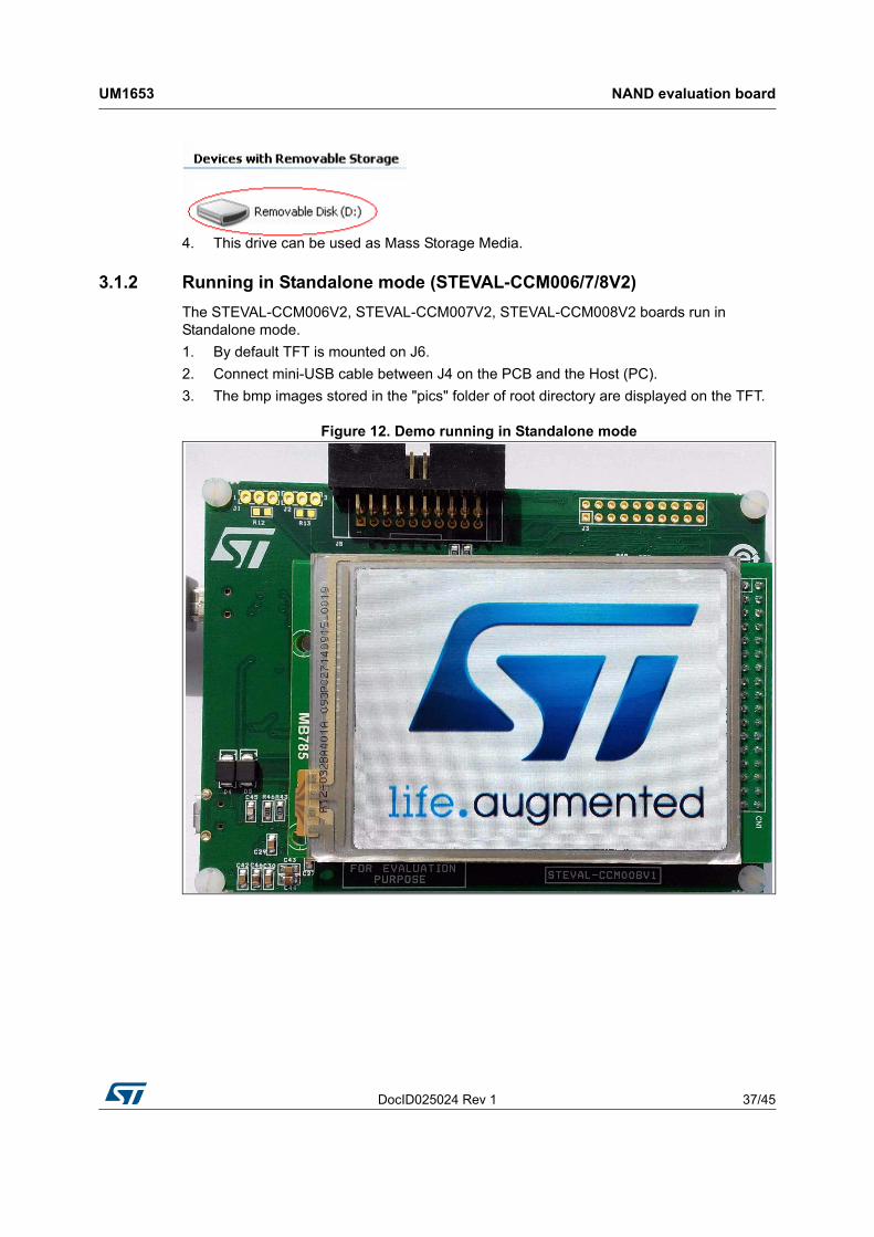
3.1.2 Running in Standalone mode (STEVAL-CCM006/7/8V2) . . . . . . . . . . . 37
3.2 Schematics . . . . . . . . . . . . . . . . . . . . . . . . . . . . . . . . . . . . . . . . . . . . . . . . 38
3.3 NAND evaluation board images . . . . . . . . . . . . . . . . . . . . . . . . . . . . . . . . 43
4 Revision history . . . . . . . . . . . . . . . . . . . . . . . . . . . . . . . . . . . . . . . . . . . 44
DocID025024 Rev 1 3/45
UM1653 List of tables
4
List of tables
Table 1. Spare area format for small NAND Flash . . . . . . . . . . . . . . . . . . . . . . . . . . . . . . . . . . . . . . . 9Table 2. Spare area format for large NAND Flash . . . . . . . . . . . . . . . . . . . . . . . . . . . . . . . . . . . . . . . 9Table 3. File system interface functions . . . . . . . . . . . . . . . . . . . . . . . . . . . . . . . . . . . . . . . . . . . . . . 17Table 4. NAND_Init . . . . . . . . . . . . . . . . . . . . . . . . . . . . . . . . . . . . . . . . . . . . . . . . . . . . . . . . . . . . . . 19Table 5. NAND_Write . . . . . . . . . . . . . . . . . . . . . . . . . . . . . . . . . . . . . . . . . . . . . . . . . . . . . . . . . . . . 19Table 6. NAND_Read . . . . . . . . . . . . . . . . . . . . . . . . . . . . . . . . . . . . . . . . . . . . . . . . . . . . . . . . . . . . 19Table 7. NAND_WriteECC . . . . . . . . . . . . . . . . . . . . . . . . . . . . . . . . . . . . . . . . . . . . . . . . . . . . . . . . 20Table 8. NAND_PostWriteECC . . . . . . . . . . . . . . . . . . . . . . . . . . . . . . . . . . . . . . . . . . . . . . . . . . . . 20Table 9. NAND_CleanLUT . . . . . . . . . . . . . . . . . . . . . . . . . . . . . . . . . . . . . . . . . . . . . . . . . . . . . . . . 20Table 10. NAND_WearLeveling . . . . . . . . . . . . . . . . . . . . . . . . . . . . . . . . . . . . . . . . . . . . . . . . . . . . . 20Table 11. SBLK_NAND_WearLeveling . . . . . . . . . . . . . . . . . . . . . . . . . . . . . . . . . . . . . . . . . . . . . . . 21Table 12. LBLK_NAND_WearLeveling. . . . . . . . . . . . . . . . . . . . . . . . . . . . . . . . . . . . . . . . . . . . . . . . 21Table 13. NAND_GetFreeBlock . . . . . . . . . . . . . . . . . . . . . . . . . . . . . . . . . . . . . . . . . . . . . . . . . . . . . 21Table 14. SBLK_NAND_ReadSpareArea. . . . . . . . . . . . . . . . . . . . . . . . . . . . . . . . . . . . . . . . . . . . . . 21Table 15. LBLK_NAND_ReadSpareArea . . . . . . . . . . . . . . . . . . . . . . . . . . . . . . . . . . . . . . . . . . . . . . 21Table 16. WriteSpareArea . . . . . . . . . . . . . . . . . . . . . . . . . . . . . . . . . . . . . . . . . . . . . . . . . . . . . . . . . 22Table 17. NAND_Copy . . . . . . . . . . . . . . . . . . . . . . . . . . . . . . . . . . . . . . . . . . . . . . . . . . . . . . . . . . . . 22Table 18. NAND_CopyBack . . . . . . . . . . . . . . . . . . . . . . . . . . . . . . . . . . . . . . . . . . . . . . . . . . . . . . . . 22Table 19. NAND_Format . . . . . . . . . . . . . . . . . . . . . . . . . . . . . . . . . . . . . . . . . . . . . . . . . . . . . . . . . . 23Table 20. NAND_PostWrite . . . . . . . . . . . . . . . . . . . . . . . . . . . . . . . . . . . . . . . . . . . . . . . . . . . . . . . . 23Table 21. SBLK_NAND_PostWrite . . . . . . . . . . . . . . . . . . . . . . . . . . . . . . . . . . . . . . . . . . . . . . . . . . . 23Table 22. LBLK_NAND_PostWrite . . . . . . . . . . . . . . . . . . . . . . . . . . . . . . . . . . . . . . . . . . . . . . . . . . . 23Table 23. NAND_GarbageCollection . . . . . . . . . . . . . . . . . . . . . . . . . . . . . . . . . . . . . . . . . . . . . . . . . 24Table 24. NAND_UpdateWearLevelCounter . . . . . . . . . . . . . . . . . . . . . . . . . . . . . . . . . . . . . . . . . . . 24Table 25. NAND_ConvertPhyAddress . . . . . . . . . . . . . . . . . . . . . . . . . . . . . . . . . . . . . . . . . . . . . . . . 24Table 26. NAND_BuildLUT. . . . . . . . . . . . . . . . . . . . . . . . . . . . . . . . . . . . . . . . . . . . . . . . . . . . . . . . . 24Table 27. SBLK_NAND_BuildLUT . . . . . . . . . . . . . . . . . . . . . . . . . . . . . . . . . . . . . . . . . . . . . . . . . . . 25Table 28. LBLK_NAND_BuildLUT . . . . . . . . . . . . . . . . . . . . . . . . . . . . . . . . . . . . . . . . . . . . . . . . . . . 25Table 29. GetParity . . . . . . . . . . . . . . . . . . . . . . . . . . . . . . . . . . . . . . . . . . . . . . . . . . . . . . . . . . . . . . . 25Table 30. Swap. . . . . . . . . . . . . . . . . . . . . . . . . . . . . . . . . . . . . . . . . . . . . . . . . . . . . . . . . . . . . . . . . . 25Table 31. WritePage . . . . . . . . . . . . . . . . . . . . . . . . . . . . . . . . . . . . . . . . . . . . . . . . . . . . . . . . . . . . . . 26Table 32. SBLK_NAND_WritePage . . . . . . . . . . . . . . . . . . . . . . . . . . . . . . . . . . . . . . . . . . . . . . . . . . 26Table 33. LBLK_NAND_WritePage . . . . . . . . . . . . . . . . . . . . . . . . . . . . . . . . . . . . . . . . . . . . . . . . . . 26Table 34. ReadPage. . . . . . . . . . . . . . . . . . . . . . . . . . . . . . . . . . . . . . . . . . . . . . . . . . . . . . . . . . . . . . 27Table 35. SBLK_NAND_ReadPage . . . . . . . . . . . . . . . . . . . . . . . . . . . . . . . . . . . . . . . . . . . . . . . . . . 27Table 36. LBLK_NAND_ReadPage . . . . . . . . . . . . . . . . . . . . . . . . . . . . . . . . . . . . . . . . . . . . . . . . . . 27Table 37. BitCount . . . . . . . . . . . . . . . . . . . . . . . . . . . . . . . . . . . . . . . . . . . . . . . . . . . . . . . . . . . . . . . 27Table 38. FSMC_SelectNANDType . . . . . . . . . . . . . . . . . . . . . . . . . . . . . . . . . . . . . . . . . . . . . . . . . . 28Table 39. FSMC_NAND_NON_ONFI_Compliance . . . . . . . . . . . . . . . . . . . . . . . . . . . . . . . . . . . . . . 28Table 40. FSMC_NAND_Init. . . . . . . . . . . . . . . . . . . . . . . . . . . . . . . . . . . . . . . . . . . . . . . . . . . . . . . . 28Table 41. FSMC_NAND_ReadID . . . . . . . . . . . . . . . . . . . . . . . . . . . . . . . . . . . . . . . . . . . . . . . . . . . . 28Table 42. FSMC_NAND_WriteSmallPage . . . . . . . . . . . . . . . . . . . . . . . . . . . . . . . . . . . . . . . . . . . . . 29Table 43. FSMC_NAND_ReadSmallPage . . . . . . . . . . . . . . . . . . . . . . . . . . . . . . . . . . . . . . . . . . . . . 29Table 44. FSMC_NAND_WriteSpareArea . . . . . . . . . . . . . . . . . . . . . . . . . . . . . . . . . . . . . . . . . . . . . 30Table 45. FSMC_NAND_ReadSpareArea . . . . . . . . . . . . . . . . . . . . . . . . . . . . . . . . . . . . . . . . . . . . . 30Table 46. FSMC_NAND_EraseBlock . . . . . . . . . . . . . . . . . . . . . . . . . . . . . . . . . . . . . . . . . . . . . . . . . 30Table 47. FSMC_NAND_Reset . . . . . . . . . . . . . . . . . . . . . . . . . . . . . . . . . . . . . . . . . . . . . . . . . . . . . 31Table 48. FSMC_NAND_GetStatus . . . . . . . . . . . . . . . . . . . . . . . . . . . . . . . . . . . . . . . . . . . . . . . . . . 31
List of tables UM1653
4/45 DocID025024 Rev 1
Table 49. FSMC_SBLK_NAND_CopyBack . . . . . . . . . . . . . . . . . . . . . . . . . . . . . . . . . . . . . . . . . . . . 31Table 50. FSMC_LBLK_NAND_CopyBack . . . . . . . . . . . . . . . . . . . . . . . . . . . . . . . . . . . . . . . . . . . . 32Table 51. FSMC_NAND_ReadStatus. . . . . . . . . . . . . . . . . . . . . . . . . . . . . . . . . . . . . . . . . . . . . . . . . 32Table 52. FSMC_NAND_AddressIncrement . . . . . . . . . . . . . . . . . . . . . . . . . . . . . . . . . . . . . . . . . . . 32Table 53. FSMC_NAND_ONFI_Compliance . . . . . . . . . . . . . . . . . . . . . . . . . . . . . . . . . . . . . . . . . . . 32Table 54. FSMC_SBLK_NAND_SendAddress. . . . . . . . . . . . . . . . . . . . . . . . . . . . . . . . . . . . . . . . . . 33Table 55. FSMC_LBLK_NAND_SendAddress . . . . . . . . . . . . . . . . . . . . . . . . . . . . . . . . . . . . . . . . . . 33Table 56. Supported NAND Flash . . . . . . . . . . . . . . . . . . . . . . . . . . . . . . . . . . . . . . . . . . . . . . . . . . . 34Table 57. NAND Flash driver file code size . . . . . . . . . . . . . . . . . . . . . . . . . . . . . . . . . . . . . . . . . . . . 34Table 58. Document revision history . . . . . . . . . . . . . . . . . . . . . . . . . . . . . . . . . . . . . . . . . . . . . . . . . 44
DocID025024 Rev 1 5/45
UM1653 List of figures
5
List of figures
Figure 1. Application architecture . . . . . . . . . . . . . . . . . . . . . . . . . . . . . . . . . . . . . . . . . . . . . . . . . . . . 6Figure 2. BOT protocol architecture. . . . . . . . . . . . . . . . . . . . . . . . . . . . . . . . . . . . . . . . . . . . . . . . . . . 7Figure 3. NAND block architecture . . . . . . . . . . . . . . . . . . . . . . . . . . . . . . . . . . . . . . . . . . . . . . . . . . . 9Figure 4. Flow of wear leveling mechanism for STEVAL-CCM006V1 . . . . . . . . . . . . . . . . . . . . . . . . 12Figure 5. Flow of wear leveling mechanism for STEVAL-CCM007V1/ 008V1. . . . . . . . . . . . . . . . . . 13Figure 6. Example of decomposition of a data packet . . . . . . . . . . . . . . . . . . . . . . . . . . . . . . . . . . . . 15Figure 7. Flow chart for error detection and correction . . . . . . . . . . . . . . . . . . . . . . . . . . . . . . . . . . . 16Figure 8. Flow chart for bad block management . . . . . . . . . . . . . . . . . . . . . . . . . . . . . . . . . . . . . . . . 17Figure 9. Flow chart for File System . . . . . . . . . . . . . . . . . . . . . . . . . . . . . . . . . . . . . . . . . . . . . . . . . 18Figure 10. Evaluation board: top side . . . . . . . . . . . . . . . . . . . . . . . . . . . . . . . . . . . . . . . . . . . . . . . . . 35Figure 11. Evaluation board: bottom side . . . . . . . . . . . . . . . . . . . . . . . . . . . . . . . . . . . . . . . . . . . . . . 36Figure 12. Demo running in Standalone mode . . . . . . . . . . . . . . . . . . . . . . . . . . . . . . . . . . . . . . . . . . 37Figure 13. Microcontroller schematic . . . . . . . . . . . . . . . . . . . . . . . . . . . . . . . . . . . . . . . . . . . . . . . . . . 38Figure 14. USB Full Speed schematic . . . . . . . . . . . . . . . . . . . . . . . . . . . . . . . . . . . . . . . . . . . . . . . . . 38Figure 15. USB High Speed schematic . . . . . . . . . . . . . . . . . . . . . . . . . . . . . . . . . . . . . . . . . . . . . . . . 39Figure 16. Touch Screen schematic . . . . . . . . . . . . . . . . . . . . . . . . . . . . . . . . . . . . . . . . . . . . . . . . . . 39Figure 17. TFT Connector schematic . . . . . . . . . . . . . . . . . . . . . . . . . . . . . . . . . . . . . . . . . . . . . . . . . 40Figure 18. Power schematic . . . . . . . . . . . . . . . . . . . . . . . . . . . . . . . . . . . . . . . . . . . . . . . . . . . . . . . . 40Figure 19. NAND Flash schematic. . . . . . . . . . . . . . . . . . . . . . . . . . . . . . . . . . . . . . . . . . . . . . . . . . . . 41Figure 20. NAND Flash Signals schematic . . . . . . . . . . . . . . . . . . . . . . . . . . . . . . . . . . . . . . . . . . . . . 42Figure 21. JTAG schematic . . . . . . . . . . . . . . . . . . . . . . . . . . . . . . . . . . . . . . . . . . . . . . . . . . . . . . . . . 42Figure 22. Top side of PCB . . . . . . . . . . . . . . . . . . . . . . . . . . . . . . . . . . . . . . . . . . . . . . . . . . . . . . . . . 43Figure 23. Bottom side of PCB . . . . . . . . . . . . . . . . . . . . . . . . . . . . . . . . . . . . . . . . . . . . . . . . . . . . . . 43
STM32 NAND driver blocks UM1653
6/45 DocID025024 Rev 1
1 STM32 NAND driver blocks
This document describes how to connect a NAND Flash device to an STM32 family microcontroller and communicate using FSMC. NAND driver library for STM32 is a generic library where STM32 can access NAND with some advanced features like garbage collection, wear leveling, bad block management, ECC checking etc. The library supports both FAT file system and USB MSC device.
Figure 1. Application architecture
1.1 STM32 USB peripheral
The STM32F embeds a USB peripheral that supports USB full-speed and high speed.The development of Endpoint and support suspend / resume are configured by software. The USB device provides a connection between the host and the function implemented by the microcontroller. Data transfer between the host and the memory system is through a dedicated packet buffer memory accessed directly from the USB device. The size of buffer memory is dependent on the number of endpoints used and the maximum packet size. This dedicated memory is 512 bytes.
LLD: Low level driver
ECC: Error correction code
BBM: Bad block management
MS33215V1
STM32 Lib
Flash translation layer
Hardware Adaption Layer
NAND Flash Device
FTL Interface
Garbage collection Wear Leveling
LLD ECC BBM
File System
DocID025024 Rev 1 7/45
UM1653 STM32 NAND driver blocks
44
1.2 USB mass storage
The USB device is provided to the host as a particular class, which determines how the host cross reacts with the embedded system.
In our case, the USB device must appear in the driver as a Mass Storage Class USB, which defines that SCSI commands will be used with the protocol “bulk-only transport” (BOT).
Bulk-only-transport (BOT)
A general BOT transaction is based on a simple basic state machine. It begins with ready state (idle state) and if a CBW is received from the host three cases can be managed:
DATA-OUT-STAGE: when direction flag is set to 0, Device shall prepare itself to receive an amount of data indicated in dCBWDataTransferLength in the CBW block. At the end of data transfer a CSW is returned with the remaining data length and the STATUS field.
DATA-IN-STAGE: when direction flag is set to 1, Device shall prepare itself to send an amount of data indicated in dCBWDataTransferLength in the CBW block. At the end of data transfer a CSW is returned with the remaining data length and the STATUS field.
ZERO DATA: no data stage is needed so CSW block is sent immediately after CBW.
The BOT transport protocol encapsulates SCSI commands and transfers them in three steps:
1. Send the command block CBW.
2. Transfer data.
3. Return the status of the block CSW.
Figure 2. BOT protocol architecture
MS33216V1
Ready
Command transportCBW
Data InData Out
StatusTransport
STM32 NAND driver blocks UM1653
8/45 DocID025024 Rev 1
Bulk-Only Transport State machine
#define BOT_IDLE 0 //Idle state
#define BOT_DATA_OUT 1 //Data Out state
#define BOT_DATA_IN 2 //Data In state
#define BOT_DATA_IN_LAST 3 //Last Data In Last
#define BOT_CSW_Send 4 //Command Status Wrapper
#define BOT_ERROR 5 //error state
#define BOT_CBW_SIGNATURE 0x43425355 //1st 4 bytes of CBW pkt
#define BOT_CSW_SIGNATURE 0x53425355 //1st 4 bytes of CSW pkt
#define BOT_CBW_PACKET_LENGTH 31
#define CSW_DATA_LENGTH 13
CSW Status Definitions
#define CSW_CMD_PASSED 0x00
#define CSW_CMD_FAILED 0x01
#define CSW_PHASE_ERROR 0x02
#define SEND_CSW_DISABLE 0
#define SEND_CSW_ENABLE 1
#define DIR_IN 0
#define DIR_OUT 1
#define BOTH_DIR 2
1.3 FSMC
The FSMC block is able to communicate with the synchronous and asynchronous memory. Its main purpose is to:
Translate the AHB protocol transactions of external devices
Respect the access time of external devices
The FSMC provides a single access to an external device.
The FSMC has four blocks:
AHB Interface
Controller NOR Flash / PSRAM
Controller NAND Flash / PC Card
Interface to external device
The FSMC generates the appropriate signals to drive the NAND Flash memory.
The FSMC controller consists of two blocks of code error correction hardware. They reduce the workload on the host processor when processing code error correction by the system software. These two blocks are identical and are respectively associated with banks 2 and 3. The ECC algorithm used in the FSMC can perform 1- and 2-bit error detection.
DocID025024 Rev 1 9/45
UM1653 STM32 NAND driver blocks
44
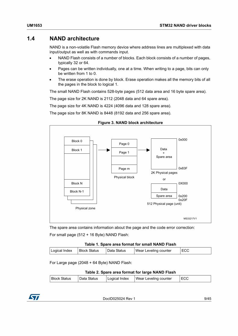
1.4 NAND architecture
NAND is a non-volatile Flash memory device where address lines are multiplexed with data input/output as well as with commands input.
NAND Flash consists of a number of blocks. Each block consists of a number of pages, typically 32 or 64.
Pages can be written individually, one at a time. When writing to a page, bits can only be written from 1 to 0.
The erase operation is done by block. Erase operation makes all the memory bits of all the pages in the block to logical 1.
The small NAND Flash contains 528-byte pages (512 data area and 16 byte spare area).
The page size for 2K NAND is 2112 (2048 data and 64 spare area).
The page size for 4K NAND is 4224 (4096 data and 128 spare area).
The page size for 8K NAND is 8448 (8192 data and 256 spare area).
Figure 3. NAND block architecture
The spare area contains information about the page and the code error correction:
For small page (512 + 16 Byte) NAND Flash:
For Large page (2048 + 64 Byte) NAND Flash:
Table 1. Spare area format for small NAND Flash
Logical Index Block Status Data Status Wear Leveling counter ECC
Table 2. Spare area format for large NAND Flash
Block Status Data Status Logical Index Wear Leveling counter ECC
MS33217V1
Page 0
Page 1
Page m
Physical block
Block 0
Block 1
Block N
Block N-1
Physical zone
Data +
Spare area
Data
Spare area
2K Physical pages
512 Physical page (unit)
0x000
0x83F
0X000
0x2000x20F
or
STM32 NAND driver blocks UM1653
10/45 DocID025024 Rev 1
The Logical Index contains the logical address of the block.
The Block Status returns the status of the block if it is valid or not.
The Data Status informs if the page is valid or invalid.
Wear Leveling Counter is the number of times the block has been erased.
The ECC is the error correction code calculated for each page.
NAND INTERFACE
x8 or x16 bus width
Multiplexed Address/ Data
Pinout compatibility for all densities
SUPPLY VOLTAGE
1.8V device: VCC = 1.65 to 1.95V
3.0V device: VCC = 2.7 to 3.6V
PAGE SIZE
x8 device: (512 + 16 spare) Bytes
x16 device: (256 + 8 spare) Words
x8 device: (2048 + 64 spare) Bytes
x16 device: (1024 + 32 spare) Words
1.5 NAND pin mapping
I/O 8-15 Data Input/Outputs: for x16 devices. The I/O pins are used to input data, address, command and output data during read operation.
I/O 0-7 Data Input/Outputs: Address Inputs, or Command Inputs for x8 and x16 devices.
ALE Address Latch Enable: When active, an address can be written.
CLE Command Latch Enable: This pin should be LOW while writing commands to the command register.
CE/ Chip Enable: The CE input enables the device. Signal is active low. If the signal is inactive the device will be in standby.
RE/ Read Enable: The RE input is the serial data out control. Signal is active low to out data.
RB/ Ready/Busy (open-drain output) The RB output provides the status of the device operation. It is an open drain output, hence should be connected to a GPIO with pull-up.
LOW: a program, erase or read operation is in process.
HIGH: the process is complete.
WE/ Write Enable: The WE input controls write operations to I/O port. Commands, data and address are latched on the rising edge of WE.
WP/ Write Protect: Typically connected to Vcc, but may also be connected to a GPIO.

DocID025024 Rev 1 11/45
UM1653 NAND driver firmware modules
44
2 NAND driver firmware modules
The NAND driver library has the following modules:
1. Garbage collection
2. Wear leveling
3. Bad block management
4. ECC check
5. LUT
6. FAT file system
2.1 Garbage collection
The Garbage Collection software copies the valid data into a new (free) area and erases the original invalid data.
Garbage Collection is performed when a virtual block is full or the number of free pages in the whole device is lower than a specified threshold value.
The basic operations involved in Garbage Collection are the following:
1. The virtual blocks meeting the conditions are selected for erasure.
2. The valid physical pages are copied into a free area.
3. The selected physical blocks are erased.
As virtual blocks can contain more than one physical block, the Garbage Collection may erase more than one physical block.
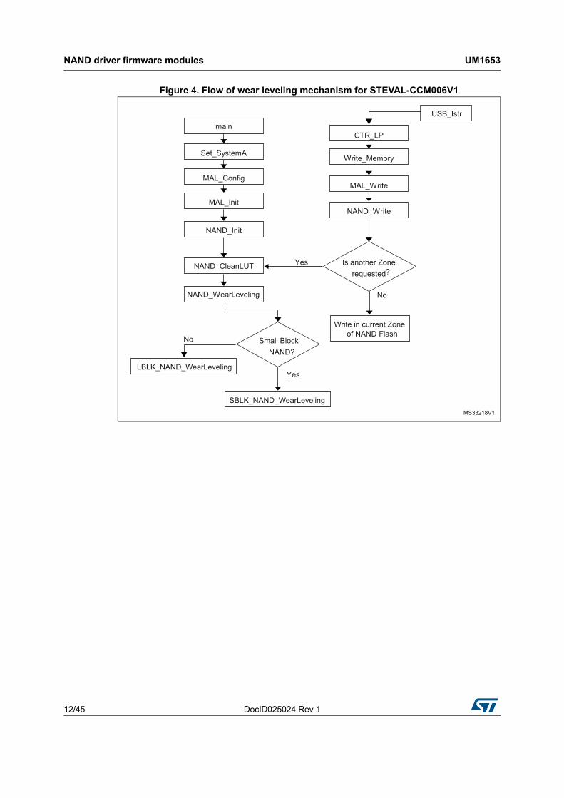
2.2 Wear leveling
Wear leveling is a technique to increase the lifetime of NAND Flash memory. The number of reliable write cycles in NAND Flash is 100,000 erase/write cycles. If some of the blocks are written repeatedly, wearing of these blocks will happen earlier than other blocks. To balance the erase cycles over all the blocks, a wear leveling technique is introduced.
All new data is written to the empty blocks. The memory controller selects the new empty block based on the number of write / erase cycles it has experienced.
After the new data is written, the controller updates the LUT to point to the position of the selected physical block. The block containing the old data is erased and the number of write/erase cycles increments.
NAND driver firmware modules UM1653
12/45 DocID025024 Rev 1
Figure 4. Flow of wear leveling mechanism for STEVAL-CCM006V1
MS33218V1
main
Set_SystemA
MAL_Config
MAL_Init
NAND_Init
NAND_CleanLUT
NAND_WearLeveling
SBLK_NAND_WearLeveling
LBLK_NAND_WearLeveling
Small BlockNAND?
USB_Istr
CTR_LP
Write_Memory
MAL_Write
NAND_Write
Is another Zonerequested?
Write in current Zoneof NAND Flash
No
Yes
Yes
No
DocID025024 Rev 1 13/45
UM1653 NAND driver firmware modules
44
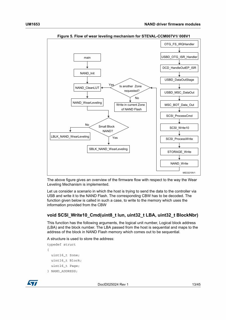
Figure 5. Flow of wear leveling mechanism for STEVAL-CCM007V1/ 008V1
The above figure gives an overview of the firmware flow with respect to the way the Wear Leveling Mechanism is implemented.
Let us consider a scenario in which the host is trying to send the data to the controller via USB and write it to the NAND Flash. The corresponding CBW has to be decoded. The function given below is called in such a case, to write to the memory which uses the information provided from the CBW
void SCSI_Write10_Cmd(uint8_t lun, uint32_t LBA, uint32_t BlockNbr)
This function has the following arguments, the logical unit number, Logical block address (LBA) and the block number. The LBA passed from the host is sequential and maps to the address of the block in NAND Flash memory which comes out to be sequential.
A structure is used to store the address:
typedef struct
{
uint16_t Zone;
uint16_t Block;
uint16_t Page;
} NAND_ADDRESS;
main
NAND_Init
NAND_CleanLUT
NAND_WearLeveling
SBLK_NAND_WearLeveling
LBLK_NAND_WearLeveling
Small BlockNAND?
OTG_FS_IRQHandler
USBD_OTG_ISR_Handler
DCD_HandleOutEP_ISR
USBD_DataOutStage
USBD_MSC_DataOut
Is another Zonerequested?
Write in current Zoneof NAND Flash
Yes
Yes
No
SCSI_ProcessCmd
SCSI_Write10
SCSI_ProcessWrite
STORAGE_Write
NAND_Write
MSC_BOT_Data_Out
No
MS33219V1
NAND driver firmware modules UM1653
14/45 DocID025024 Rev 1
NAND_ADDRESS NAND_GetAddress (uint32_t Address)
The above function translates a logical address into a physical one and stores it in a structure element of type NAND_ADDRESS.
While writing to the NAND, the wear level algorithm should return the block to be written of which the erase count is least. To maintain the list of USED, FREE and BAD blocks an array is maintained: LUT[ ].
The previously fetched address for writing, and the free block obtained with least erase counts are swapped in LUT and updated, this ensures that the write takes place at the block with least erase count.
uint16_t NAND_GetFreeBlock (void)
The above function is called to get the free block for swap. The function returns the first free block it finds in the LUT[ ]. This implies that the LUT[ ] should have the free blocks arranged in the increasing order of erase count. The LUT[ ] is updated by the following function.
uint16_t NAND_BuildLUT (uint8_t ZoneNbr)
The above function arranges the bad block at the bottom of the array and the used and free blocks are located in the upper part of the array.
uint16_t NAND_WearLeveling (void)
The above function sorts the free blocks in the ascending order based on the wear level count. Now, the free block used for writing in the NAND would be the one with the least erase count.
2.3 ECC
Unlike NOR Flash memory that does not require error correction code, NAND memory needs to ensure data integrity.
The disadvantage of the NAND configuration is that when a cell is read, the sense amplifier detects a signal much lower than for the NOR configuration because many transistors are in series. Therefore access to a cell is not straightforward and must necessarily go through all the cells in series which reduces precision and makes code error correction required.
There are three error correction codes:
The Hamming code can correct only one bit error.
The Reed Solomon code can correct more errors.
The BCH code can correct many errors and is more efficient than Reed Solomon.
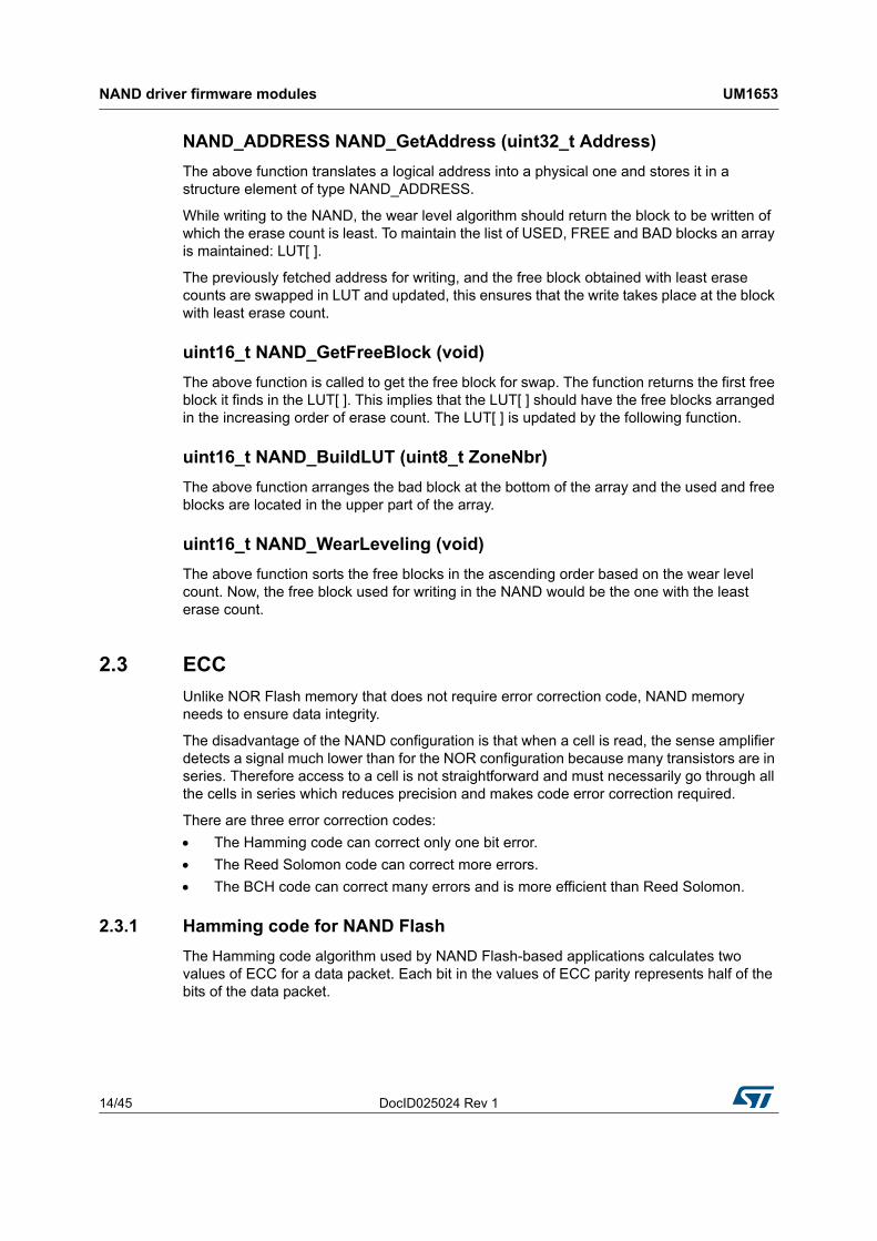
2.3.1 Hamming code for NAND Flash
The Hamming code algorithm used by NAND Flash-based applications calculates two values of ECC for a data packet. Each bit in the values of ECC parity represents half of the bits of the data packet.
DocID025024 Rev 1 15/45
UM1653 NAND driver firmware modules
44
For one byte
The trick is how the data bits are partitioned for each of the parity calculations. To calculate ECC, the data bits are first divided into halves, quarters, eighths and so on until you reach the bit unit.
Figure 6. Example of decomposition of a data packet
After the partition of the data packet, the parity of each group is calculated to generate two values of ECC. The results are concatenated to form the ECC values.
ECC even = 0 ^ 1 ^ 0 ^ 1, 0 ^ 1 ^ 0 ^ 1, 1 ^ 1 ^ 1 ^ 1 = 000ECC odd = 0 ^ 1 ^ 0 ^ 1, 0 ^ 1 ^ 0 ^ 1, 0 ^ 0 ^ 0 ^ 0 = 000
These ECC bits allow us to identify the error position when the data packet is analyzed at a later date. Data packets require larger number of ECC values. Each data packet of 2n-bit ECC requires a value of n bits.
Based on this calculation, both the data packet and the ECC values are programmed into the NAND Flash memory. Later, when the data packet is read from the NAND, the ECC values are recalculated. Data corruption is indicated when the values of the newly calculated ECC differ from those programmed into the NAND Flash.
Applying “exclusive or” to all four values of ECC (two old and two new), one can determine whether one or more bits have been corrupted. If the result is 000 there is no corruption. If the result is 111 then a single bit is wrong. If two or more bits were damaged, this code allows the detection of two errors and the correction of only one bit.
ECCeven (old) ^ ECCodd (old) ^ ECCeven (new) ^ ECCodd (new)
When the result shows that a bit has been corrupted, the address of this bit can be identified by the application of “exclusive or” on both ECC odd values
ECCodd (old) ^ ECCodd (new)
The erroneous bit position is identified by the position of the 1 in the "exclusive or" value.
For a package of several bytes
As the size of data packets increases, the Hamming algorithm becomes more efficient. Each doubling of the data packet requires two additional bits in the ECC. A data packet size of 512 bytes (the size of a page of the NAND memory used) requires 24 bits of ECC. The extension of a 1 byte packet to a 512 byte packet requires only a change to the size of data partitions, the algorithm remains the same.
MS33220V1
Bit position
Even bits
Even quarters
Even halves
0
0
0
1
1
1
0
0
0
1
1
1
0
0
0
1
1
1
0
0
0
1
1
1
01234567
Odd bits
Odd quarters
Odd halves
Data packet 0 1 0 1 0 1 0 1
NAND driver firmware modules UM1653
16/45 DocID025024 Rev 1
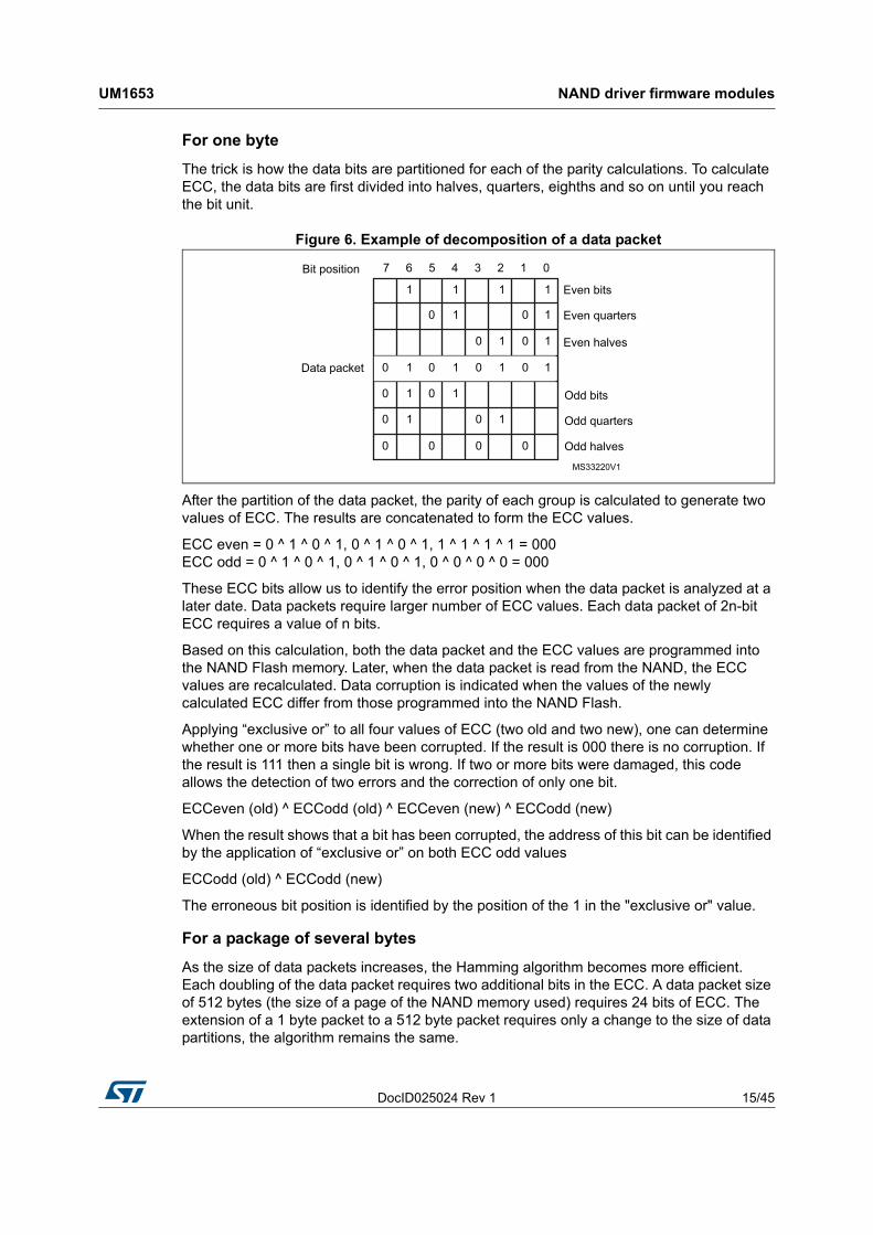
2.3.2 Error detection and correction
Figure 7. Flow chart for error detection and correction
with new ECCXOR previous ECC
New ECC generatedduring read
All results= zero?
Yes
>1 bit= zero?
12 bit= one?
No No
No
No Error Correctable error
24 bit data = 0 12 bit data = 1 All other
Non Correctable error
23 bit data = 1
ECC Error
MS33221V1
DocID025024 Rev 1 17/45
UM1653 NAND driver firmware modules
44
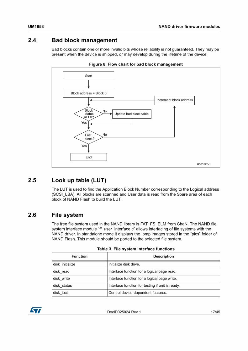
2.4 Bad block management
Bad blocks contain one or more invalid bits whose reliability is not guaranteed. They may be present when the device is shipped, or may develop during the lifetime of the device.
Figure 8. Flow chart for bad block management
2.5 Look up table (LUT)
The LUT is used to find the Application Block Number corresponding to the Logical address (SCSI_LBA). All blocks are scanned and User data is read from the Spare area of each block of NAND Flash to build the LUT.
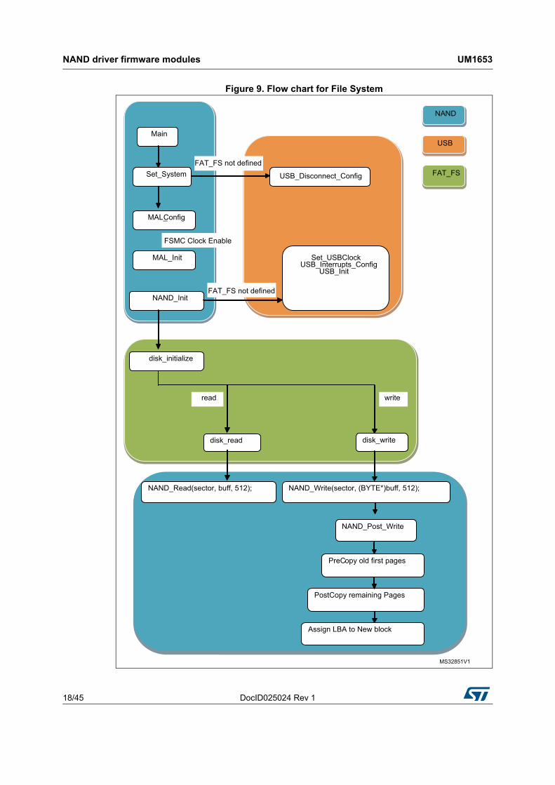
2.6 File system
The free file system used in the NAND library is FAT_FS_ELM from ChaN. The NAND file system interface module “ff_user_interface.c” allows interfacing of file systems with the NAND driver. In standalone mode it displays the .bmp images stored in the “pics” folder of NAND Flash. This module should be ported to the selected file system.
Block address = Block 0
Start
Block
=FFh?Yes
No
End
Update bad block table
Increment block address
MS33222V1
Lastblock?
Yes
No
status
Table 3. File system interface functions
Function Description
disk_initialize Initialize disk drive.
disk_read Interface function for a logical page read.
disk_write Interface function for a logical page write.
disk_status Interface function for testing if unit is ready.
disk_ioctl Control device-dependent features.
NAND driver firmware modules UM1653
18/45 DocID025024 Rev 1
Figure 9. Flow chart for File System
Main
Set_System
MAL_Config
MAL_Init
NAND_Init
USB_Disconnect_Config
Set_USBClock USB_Interrupts_Config
USB_Init
disk_initialize
read write
disk_read disk_write
NAND_Read(sector, buff, 512); NAND_Write(sector, (BYTE*)buff, 512);
NAND_Post_Write
PreCopy old first pages
PostCopy remaining Pages
Assign LBA to New block
NAND
USB
FAT_FS FAT_FS not defined
FAT_FS not defined
FSMC Clock Enable
MS32851V1
DocID025024 Rev 1 19/45
UM1653 NAND driver firmware modules
44
2.7 NAND driver files
2.7.1 nand_drv.c, nand_drv.h functions
Table 4. NAND_Init
Function name NAND_Init.
Prototype uint16_t NAND_Init(void)
Behavior description Initializes NAND Interface
Input parameter None
Output parameter
Status of NAND Initialization. This parameter can be:
– NAND_OK: when the NAND is OK.
– NAND_FAIL: when NAND fails to initialize.
Table 5. NAND_Write
Function name NAND_Write.
Prototype
uint16_t NAND_Write(uint32_t Memory_Offset,
uint8_t *Writebuff,
uint16_t Transfer_Length)
Behavior description Writes one sector at once
Input parameter
Memory_Offset: Memory Offset.
Writebuff: Pointer to the data to be written.
Transfer_Length: Number of byte to write.
Output parameter
Status of NAND Write. This parameter can be:
– NAND_OK: when the NAND Write is successful
– NAND_FAIL: when NAND fails to Write.
Table 6. NAND_Read
Function name NAND_Read.
Prototype
uint16_t NAND_Read(uint32_t Memory_Offset,
uint8_t *Readbuff,
uint16_t Transfer_Length)
Behavior description Reads sectors.
Input parameter
Memory_Offset: Memory Offset.
Readbuff: Pointer to store the read data.
Transfer_Length: Number of byte to read.
Output parameter
Status of NAND Read. This parameter can be:
– NAND_OK: when the NAND Read is successful.
– NAND_FAIL: when NAND fails to Read.
NAND driver firmware modules UM1653
20/45 DocID025024 Rev 1
.
Table 7. NAND_WriteECC
Function name NAND_WriteECC.
Prototype
uint16_t NAND_WriteECC(uint32_t Memory_Offset,
uint8_t *Writebuff,
uint16_t NumByte)
Behavior description Writes one sector & copy rest Block during ECC Correctable Error Case.
Input parameter
Memory_Offset: Memory Offset.
Writebuff: Pointer to the data to be written.
Transfer_Length: Number of byte to write.
Output parameter
Status of NAND Write. This parameter can be:
– NAND_OK: when the NAND Write is successful
– NAND_FAIL: when NAND fails to Write
Table 8. NAND_PostWriteECC
Function name NAND_PostWriteECC.
Prototype uint16_t NAND_PostWriteECC(void)
Behavior description Copies whole block after writing corrected page in ECC Correction.
Input parameter None
Output parameter Status of NAND Write.
Table 9. NAND_CleanLUT
Function name NAND_CleanLUT.
Prototype uint16_t NAND_CleanLUT (uint8_t ZoneNum)
Behavior description Rebuilds the Look Up Table.
Input parameter ZoneNbr: Zone Number to Rebuild the Look Up Table.
Output parameter
Status of NAND Build look up table. This parameter can be:
– NAND_OK: when the NAND Clean is successful.
– NAND_FAIL: when NAND fails to clean look up table.
Table 10. NAND_WearLeveling
Function name NAND_WearLeveling.
Prototype uint16_t NAND_WearLeveling (uint8_t ZoneNumber)
Behavior description Builds the Look Up Table According to the Wear Count.
Input parameter ZoneNumber: Zone Number.
Output parameter
Status of NAND wear Leveling. This parameter can be:
– NAND_OK: when the NAND wear leveling is successful.
– NAND_FAIL: when NAND fails to wear leveling.
DocID025024 Rev 1 21/45
UM1653 NAND driver firmware modules
44
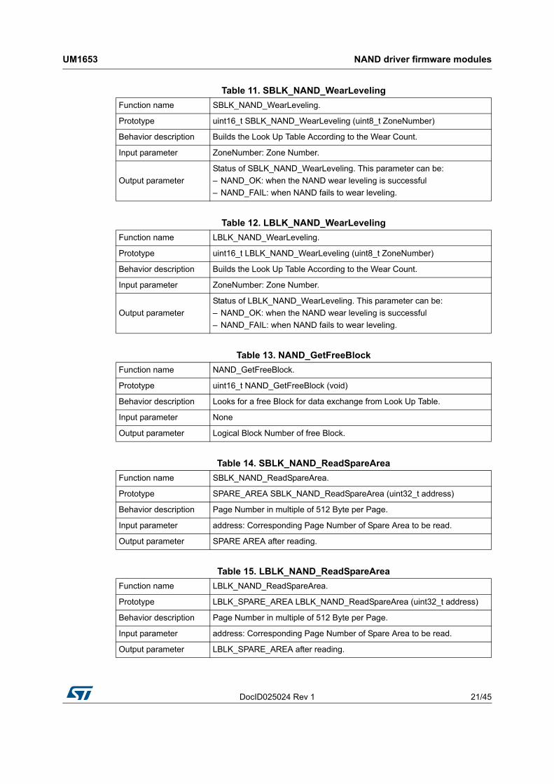
Table 11. SBLK_NAND_WearLeveling
Function name SBLK_NAND_WearLeveling.
Prototype uint16_t SBLK_NAND_WearLeveling (uint8_t ZoneNumber)
Behavior description Builds the Look Up Table According to the Wear Count.
Input parameter ZoneNumber: Zone Number.
Output parameter
Status of SBLK_NAND_WearLeveling. This parameter can be:
– NAND_OK: when the NAND wear leveling is successful
– NAND_FAIL: when NAND fails to wear leveling.
Table 12. LBLK_NAND_WearLeveling
Function name LBLK_NAND_WearLeveling.
Prototype uint16_t LBLK_NAND_WearLeveling (uint8_t ZoneNumber)
Behavior description Builds the Look Up Table According to the Wear Count.
Input parameter ZoneNumber: Zone Number.
Output parameter
Status of LBLK_NAND_WearLeveling. This parameter can be:
– NAND_OK: when the NAND wear leveling is successful
– NAND_FAIL: when NAND fails to wear leveling.
Table 13. NAND_GetFreeBlock
Function name NAND_GetFreeBlock.
Prototype uint16_t NAND_GetFreeBlock (void)
Behavior description Looks for a free Block for data exchange from Look Up Table.
Input parameter None
Output parameter Logical Block Number of free Block.
Table 14. SBLK_NAND_ReadSpareArea
Function name SBLK_NAND_ReadSpareArea.
Prototype SPARE_AREA SBLK_NAND_ReadSpareArea (uint32_t address)
Behavior description Page Number in multiple of 512 Byte per Page.
Input parameter address: Corresponding Page Number of Spare Area to be read.
Output parameter SPARE AREA after reading.
Table 15. LBLK_NAND_ReadSpareArea
Function name LBLK_NAND_ReadSpareArea.
Prototype LBLK_SPARE_AREA LBLK_NAND_ReadSpareArea (uint32_t address)
Behavior description Page Number in multiple of 512 Byte per Page.
Input parameter address: Corresponding Page Number of Spare Area to be read.
Output parameter LBLK_SPARE_AREA after reading.
NAND driver firmware modules UM1653
22/45 DocID025024 Rev 1
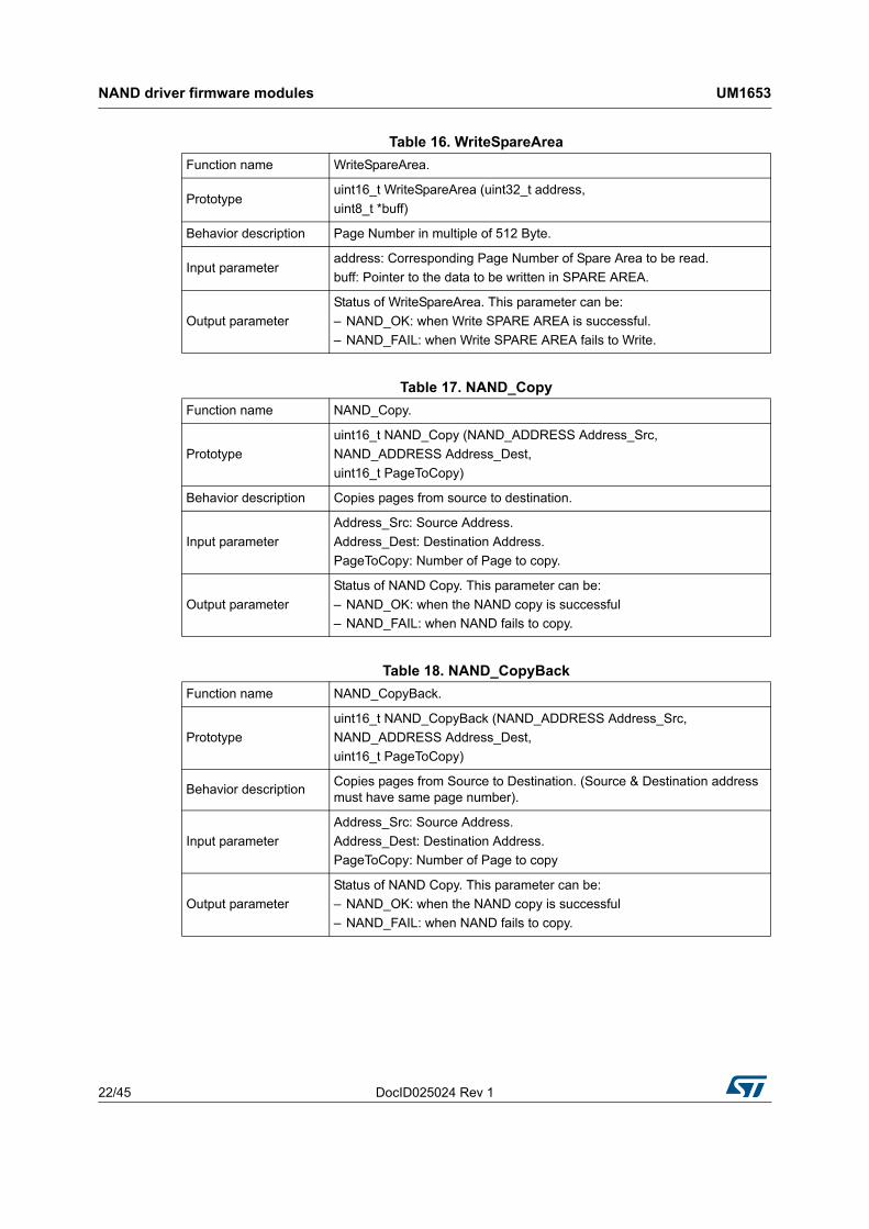
Table 16. WriteSpareArea
Function name WriteSpareArea.
Prototypeuint16_t WriteSpareArea (uint32_t address,
uint8_t *buff)
Behavior description Page Number in multiple of 512 Byte.
Input parameteraddress: Corresponding Page Number of Spare Area to be read.
buff: Pointer to the data to be written in SPARE AREA.
Output parameter
Status of WriteSpareArea. This parameter can be:
– NAND_OK: when Write SPARE AREA is successful.
– NAND_FAIL: when Write SPARE AREA fails to Write.
Table 17. NAND_Copy
Function name NAND_Copy.
Prototype
uint16_t NAND_Copy (NAND_ADDRESS Address_Src,
NAND_ADDRESS Address_Dest,
uint16_t PageToCopy)
Behavior description Copies pages from source to destination.
Input parameter
Address_Src: Source Address.
Address_Dest: Destination Address.
PageToCopy: Number of Page to copy.
Output parameter
Status of NAND Copy. This parameter can be:
– NAND_OK: when the NAND copy is successful
– NAND_FAIL: when NAND fails to copy.
Table 18. NAND_CopyBack
Function name NAND_CopyBack.
Prototype
uint16_t NAND_CopyBack (NAND_ADDRESS Address_Src,
NAND_ADDRESS Address_Dest,
uint16_t PageToCopy)
Behavior descriptionCopies pages from Source to Destination. (Source & Destination address must have same page number).
Input parameter
Address_Src: Source Address.
Address_Dest: Destination Address.
PageToCopy: Number of Page to copy
Output parameter
Status of NAND Copy. This parameter can be:
– NAND_OK: when the NAND copy is successful
– NAND_FAIL: when NAND fails to copy.
DocID025024 Rev 1 23/45
UM1653 NAND driver firmware modules
44
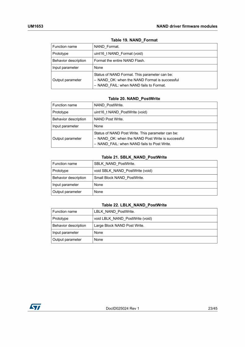
Table 19. NAND_Format
Function name NAND_Format.
Prototype uint16_t NAND_Format (void)
Behavior description Format the entire NAND Flash.
Input parameter None
Output parameter
Status of NAND Format. This parameter can be:
– NAND_OK: when the NAND Format is successful
– NAND_FAIL: when NAND fails to Format.
Table 20. NAND_PostWrite
Function name NAND_PostWrite.
Prototype uint16_t NAND_PostWrite (void)
Behavior description NAND Post Write.
Input parameter None
Output parameter
Status of NAND Post Write. This parameter can be:
– NAND_OK: when the NAND Post Write is successful
– NAND_FAIL: when NAND fails to Post Write.
Table 21. SBLK_NAND_PostWrite
Function name SBLK_NAND_PostWrite.
Prototype void SBLK_NAND_PostWrite (void)
Behavior description Small Block NAND_PostWrite.
Input parameter None
Output parameter None
Table 22. LBLK_NAND_PostWrite
Function name LBLK_NAND_PostWrite.
Prototype void LBLK_NAND_PostWrite (void)
Behavior description Large Block NAND Post Write.
Input parameter None
Output parameter None
NAND driver firmware modules UM1653
24/45 DocID025024 Rev 1
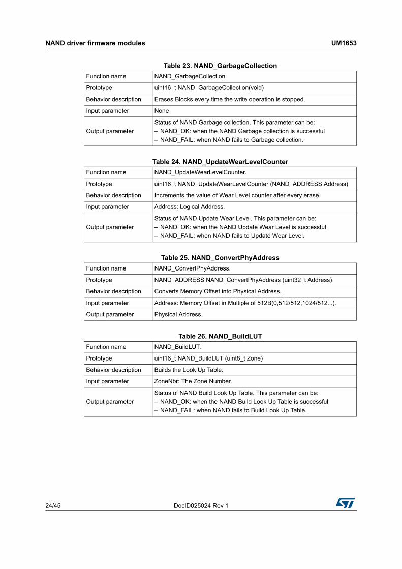
Table 23. NAND_GarbageCollection
Function name NAND_GarbageCollection.
Prototype uint16_t NAND_GarbageCollection(void)
Behavior description Erases Blocks every time the write operation is stopped.
Input parameter None
Output parameter
Status of NAND Garbage collection. This parameter can be:
– NAND_OK: when the NAND Garbage collection is successful
– NAND_FAIL: when NAND fails to Garbage collection.
Table 24. NAND_UpdateWearLevelCounter
Function name NAND_UpdateWearLevelCounter.
Prototype uint16_t NAND_UpdateWearLevelCounter (NAND_ADDRESS Address)
Behavior description Increments the value of Wear Level counter after every erase.
Input parameter Address: Logical Address.
Output parameter
Status of NAND Update Wear Level. This parameter can be:
– NAND_OK: when the NAND Update Wear Level is successful
– NAND_FAIL: when NAND fails to Update Wear Level.
Table 25. NAND_ConvertPhyAddress
Function name NAND_ConvertPhyAddress.
Prototype NAND_ADDRESS NAND_ConvertPhyAddress (uint32_t Address)
Behavior description Converts Memory Offset into Physical Address.
Input parameter Address: Memory Offset in Multiple of 512B(0,512/512,1024/512...).
Output parameter Physical Address.
Table 26. NAND_BuildLUT
Function name NAND_BuildLUT.
Prototype uint16_t NAND_BuildLUT (uint8_t Zone)
Behavior description Builds the Look Up Table.
Input parameter ZoneNbr: The Zone Number.
Output parameter
Status of NAND Build Look Up Table. This parameter can be:
– NAND_OK: when the NAND Build Look Up Table is successful
– NAND_FAIL: when NAND fails to Build Look Up Table.
DocID025024 Rev 1 25/45
UM1653 NAND driver firmware modules
44
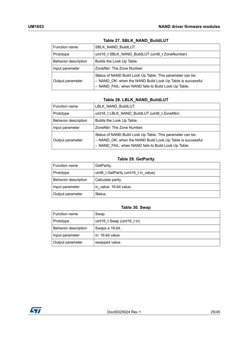
Table 27. SBLK_NAND_BuildLUT
Function name SBLK_NAND_BuildLUT.
Prototype uint16_t SBLK_NAND_BuildLUT (uint8_t ZoneNumber)
Behavior description Builds the Look Up Table.
Input parameter ZoneNbr: The Zone Number.
Output parameter
Status of NAND Build Look Up Table. This parameter can be:
– NAND_OK: when the NAND Build Look Up Table is successful
– NAND_FAIL: when NAND fails to Build Look Up Table.
Table 28. LBLK_NAND_BuildLUT
Function name LBLK_NAND_BuildLUT.
Prototype uint16_t LBLK_NAND_BuildLUT (uint8_t ZoneNbr)
Behavior description Builds the Look Up Table.
Input parameter ZoneNbr: The Zone Number.
Output parameter
Status of NAND Build Look Up Table. This parameter can be:
– NAND_OK: when the NAND Build Look Up Table is successful
– NAND_FAIL: when NAND fails to Build Look Up Table.
Table 29. GetParity
Function name GetParity.
Prototype uint8_t GetParity (uint16_t in_value)
Behavior description Calculate parity.
Input parameter in_value: 16-bit value.
Output parameter Status.
Table 30. Swap
Function name Swap.
Prototype uint16_t Swap (uint16_t in)
Behavior description Swaps a 16-bit.
Input parameter in: 16-bit value.
Output parameter swapped value.
NAND driver firmware modules UM1653
26/45 DocID025024 Rev 1
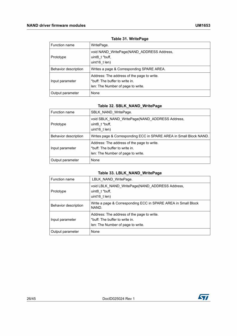
Table 31. WritePage
Function name WritePage.
Prototype
void NAND_WritePage(NAND_ADDRESS Address,
uint8_t *buff,
uint16_t len)
Behavior description Writes a page & Corresponding SPARE AREA.
Input parameter
Address: The address of the page to write.
*buff: The buffer to write in.
len: The Number of page to write.
Output parameter None
Table 32. SBLK_NAND_WritePage
Function name SBLK_NAND_WritePage.
Prototype
void SBLK_NAND_WritePage(NAND_ADDRESS Address,
uint8_t *buff,
uint16_t len)
Behavior description Writes page & Corresponding ECC in SPARE AREA in Small Block NAND.
Input parameter
Address: The address of the page to write.
*buff: The buffer to write in.
len: The Number of page to write.
Output parameter None
Table 33. LBLK_NAND_WritePage
Function name LBLK_NAND_WritePage.
Prototype
void LBLK_NAND_WritePage(NAND_ADDRESS Address,
uint8_t *buff,
uint16_t len)
Behavior descriptionWrite a page & Corresponding ECC in SPARE AREA in Small Block NAND.
Input parameter
Address: The address of the page to write.
*buff: The buffer to write in.
len: The Number of page to write.
Output parameter None
DocID025024 Rev 1 27/45
UM1653 NAND driver firmware modules
44
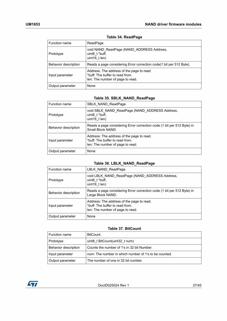
Table 34. ReadPage
Function name ReadPage.
Prototypevoid NAND_ReadPage (NAND_ADDRESS Address, uint8_t *buff, uint16_t len)
Behavior description Reads a page considering Error correction code(1 bit per 512 Byte).
Input parameterAddress: The address of the page to read.*buff: The buffer to read from.len: The number of page to read.
Output parameter None
Table 35. SBLK_NAND_ReadPage
Function name SBLK_NAND_ReadPage.
Prototypevoid SBLK_NAND_ReadPage (NAND_ADDRESS Address, uint8_t *buff, uint16_t len)
Behavior descriptionReads a page considering Error correction code (1 bit per 512 Byte) in Small Block NAND.
Input parameterAddress: The address of the page to read.*buff: The buffer to read from.len: The number of page to read.
Output parameter None
Table 36. LBLK_NAND_ReadPage
Function name LBLK_NAND_ReadPage.
Prototypevoid LBLK_NAND_ReadPage (NAND_ADDRESS Address, uint8_t *buff, uint16_t len)
Behavior descriptionReads a page considering Error correction code (1 bit per 512 Byte) in Large Block NAND.
Input parameterAddress: The address of the page to read.*buff: The buffer to read from.len: The number of page to read.
Output parameter None
Table 37. BitCount
Function name BitCount.
Prototype uint8_t BitCount(uint32_t num)
Behavior description Counts the number of 1's in 32 bit Number.
Input parameter num: The number in which number of 1's to be counted.
Output parameter The number of one in 32 bit number.
NAND driver firmware modules UM1653
28/45 DocID025024 Rev 1
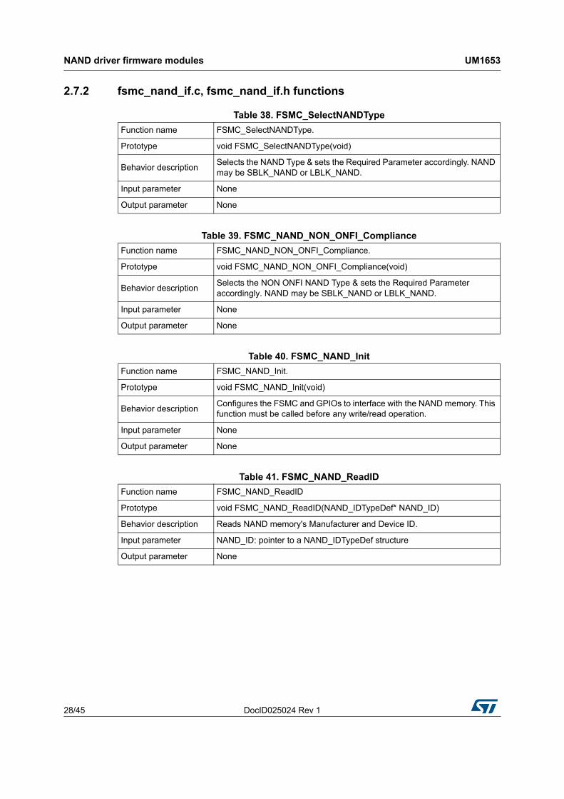
2.7.2 fsmc_nand_if.c, fsmc_nand_if.h functions
Table 38. FSMC_SelectNANDType
Function name FSMC_SelectNANDType.
Prototype void FSMC_SelectNANDType(void)
Behavior descriptionSelects the NAND Type & sets the Required Parameter accordingly. NAND may be SBLK_NAND or LBLK_NAND.
Input parameter None
Output parameter None
Table 39. FSMC_NAND_NON_ONFI_Compliance
Function name FSMC_NAND_NON_ONFI_Compliance.
Prototype void FSMC_NAND_NON_ONFI_Compliance(void)
Behavior descriptionSelects the NON ONFI NAND Type & sets the Required Parameter accordingly. NAND may be SBLK_NAND or LBLK_NAND.
Input parameter None
Output parameter None
Table 40. FSMC_NAND_Init
Function name FSMC_NAND_Init.
Prototype void FSMC_NAND_Init(void)
Behavior descriptionConfigures the FSMC and GPIOs to interface with the NAND memory. This function must be called before any write/read operation.
Input parameter None
Output parameter None
Table 41. FSMC_NAND_ReadID
Function name FSMC_NAND_ReadID
Prototype void FSMC_NAND_ReadID(NAND_IDTypeDef* NAND_ID)
Behavior description Reads NAND memory's Manufacturer and Device ID.
Input parameter NAND_ID: pointer to a NAND_IDTypeDef structure
Output parameter None
DocID025024 Rev 1 29/45
UM1653 NAND driver firmware modules
44
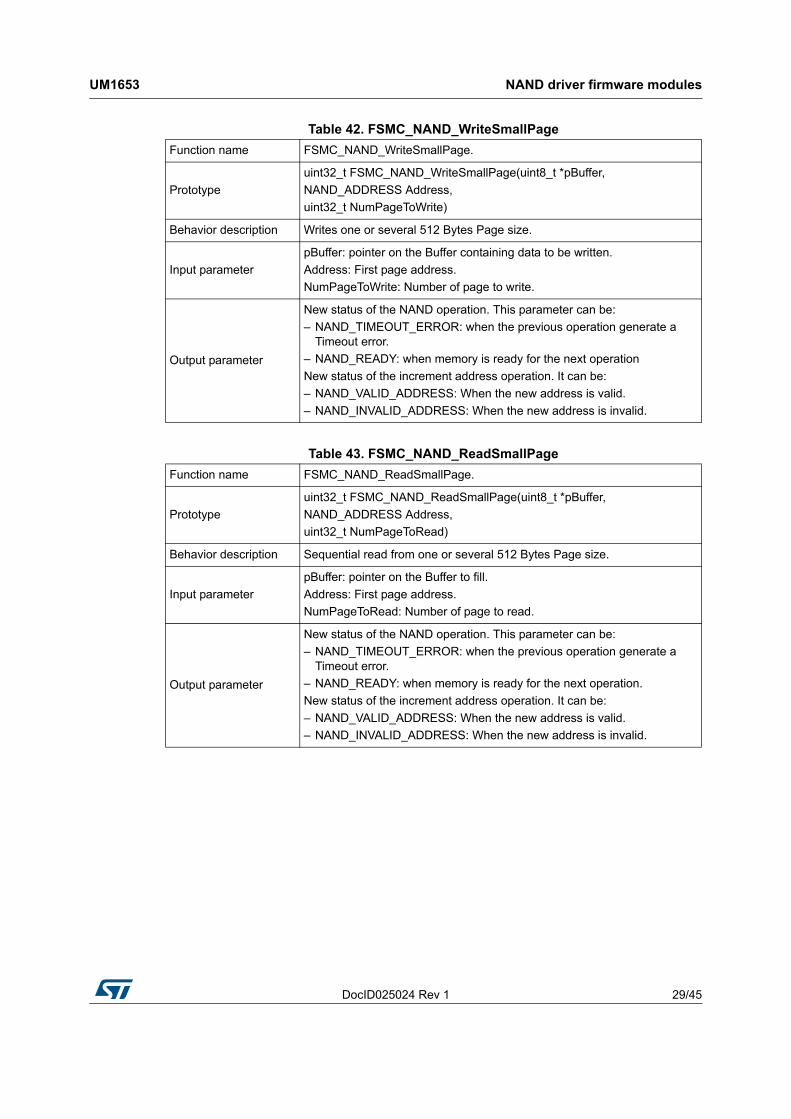
Table 42. FSMC_NAND_WriteSmallPage
Function name FSMC_NAND_WriteSmallPage.
Prototype
uint32_t FSMC_NAND_WriteSmallPage(uint8_t *pBuffer,
NAND_ADDRESS Address,
uint32_t NumPageToWrite)
Behavior description Writes one or several 512 Bytes Page size.
Input parameter
pBuffer: pointer on the Buffer containing data to be written.
Address: First page address.
NumPageToWrite: Number of page to write.
Output parameter
New status of the NAND operation. This parameter can be:
– NAND_TIMEOUT_ERROR: when the previous operation generate a Timeout error.
– NAND_READY: when memory is ready for the next operation
New status of the increment address operation. It can be:
– NAND_VALID_ADDRESS: When the new address is valid.
– NAND_INVALID_ADDRESS: When the new address is invalid.
Table 43. FSMC_NAND_ReadSmallPage
Function name FSMC_NAND_ReadSmallPage.
Prototype
uint32_t FSMC_NAND_ReadSmallPage(uint8_t *pBuffer,
NAND_ADDRESS Address,
uint32_t NumPageToRead)
Behavior description Sequential read from one or several 512 Bytes Page size.
Input parameter
pBuffer: pointer on the Buffer to fill.
Address: First page address.
NumPageToRead: Number of page to read.
Output parameter
New status of the NAND operation. This parameter can be:
– NAND_TIMEOUT_ERROR: when the previous operation generate a Timeout error.
– NAND_READY: when memory is ready for the next operation.
New status of the increment address operation. It can be:
– NAND_VALID_ADDRESS: When the new address is valid.
– NAND_INVALID_ADDRESS: When the new address is invalid.
NAND driver firmware modules UM1653
30/45 DocID025024 Rev 1
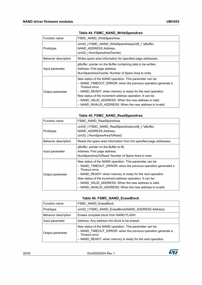
Table 44. FSMC_NAND_WriteSpareArea
Function name FSMC_NAND_WriteSpareArea.
Prototype
uint32_t FSMC_NAND_WriteSpareArea(uint8_t *pBuffer,
NAND_ADDRESS Address,
uint32_t NumSpareAreaTowrite)
Behavior description Writes spare area information for specified page addresses.
Input parameter
pBuffer: pointer on the Buffer containing data to be written.
Address: First page address.
NumSpareAreaTowrite: Number of Spare Area to write.
Output parameter
New status of the NAND operation. This parameter can be:
– NAND_TIMEOUT_ERROR: when the previous operation generate a Timeout error.
– NAND_READY: when memory is ready for the next operation
New status of the increment address operation. It can be:
– NAND_VALID_ADDRESS: When the new address is valid.
– NAND_INVALID_ADDRESS: When the new address is invalid.
Table 45. FSMC_NAND_ReadSpareArea
Function name FSMC_NAND_ReadSpareArea.
Prototype
uint32_t FSMC_NAND_ReadSpareArea(uint8_t *pBuffer,
NAND_ADDRESS Address,
uint32_t NumSpareAreaToRead)
Behavior description Reads the spare area information from the specified page addresses.
Input parameter
pBuffer: pointer on the Buffer to fill.
Address: First page address.
NumSpareAreaToRead: Number of Spare Area to read.
Output parameter
New status of the NAND operation. This parameter can be:
– NAND_TIMEOUT_ERROR: when the previous operation generated a Timeout error.
– NAND_READY: when memory is ready for the next operation
New status of the increment address operation. It can be:
– NAND_VALID_ADDRESS: When the new address is valid.
– NAND_INVALID_ADDRESS: When the new address is invalid.
Table 46. FSMC_NAND_EraseBlock
Function name FSMC_NAND_EraseBlock.
Prototype uint32_t FSMC_NAND_EraseBlock(NAND_ADDRESS Address)
Behavior description Erases complete block from NAND FLASH.
Input parameter Address: Any address into block to be erased.
Output parameter
New status of the NAND operation. This parameter can be:
– NAND_TIMEOUT_ERROR: when the previous operation generate a Timeout error.
– NAND_READY: when memory is ready for the next operation.
DocID025024 Rev 1 31/45
UM1653 NAND driver firmware modules
44
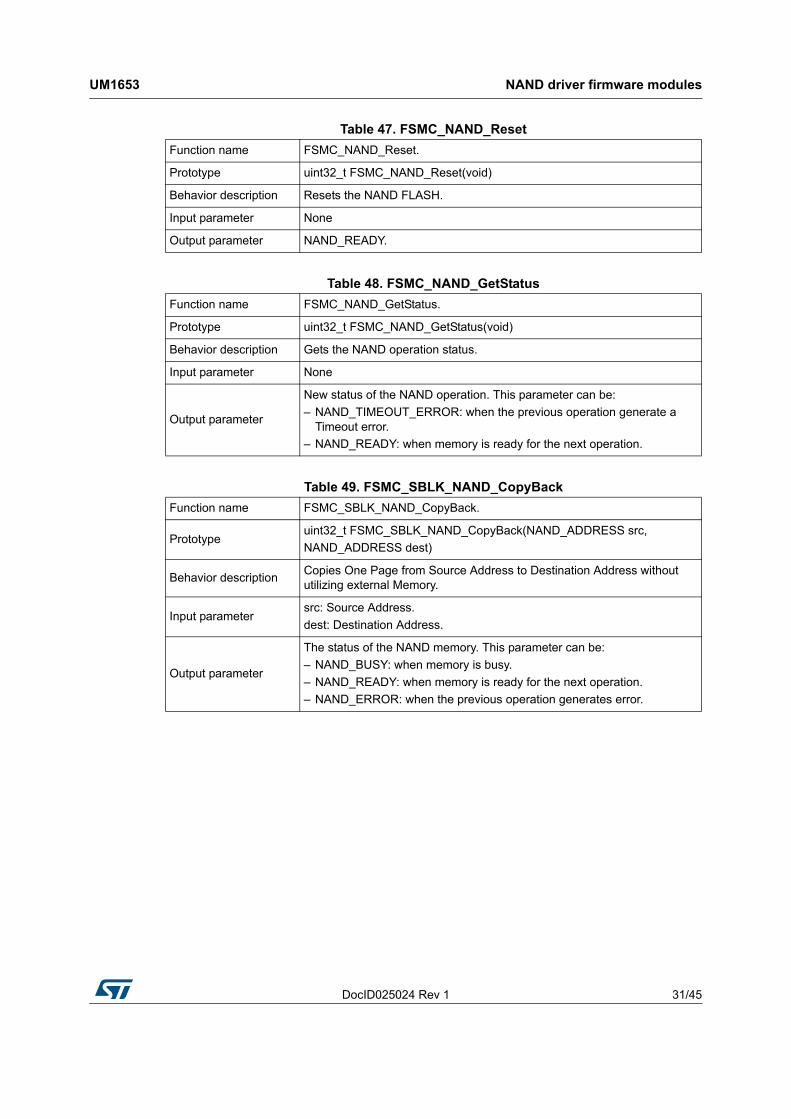
Table 47. FSMC_NAND_Reset
Function name FSMC_NAND_Reset.
Prototype uint32_t FSMC_NAND_Reset(void)
Behavior description Resets the NAND FLASH.
Input parameter None
Output parameter NAND_READY.
Table 48. FSMC_NAND_GetStatus
Function name FSMC_NAND_GetStatus.
Prototype uint32_t FSMC_NAND_GetStatus(void)
Behavior description Gets the NAND operation status.
Input parameter None
Output parameter
New status of the NAND operation. This parameter can be:
– NAND_TIMEOUT_ERROR: when the previous operation generate a Timeout error.
– NAND_READY: when memory is ready for the next operation.
Table 49. FSMC_SBLK_NAND_CopyBack
Function name FSMC_SBLK_NAND_CopyBack.
Prototypeuint32_t FSMC_SBLK_NAND_CopyBack(NAND_ADDRESS src,
NAND_ADDRESS dest)
Behavior descriptionCopies One Page from Source Address to Destination Address without utilizing external Memory.
Input parametersrc: Source Address.
dest: Destination Address.
Output parameter
The status of the NAND memory. This parameter can be:
– NAND_BUSY: when memory is busy.
– NAND_READY: when memory is ready for the next operation.
– NAND_ERROR: when the previous operation generates error.
NAND driver firmware modules UM1653
32/45 DocID025024 Rev 1
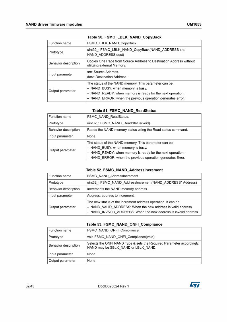
Table 50. FSMC_LBLK_NAND_CopyBack
Function name FSMC_LBLK_NAND_CopyBack.
Prototypeuint32_t FSMC_LBLK_NAND_CopyBack(NAND_ADDRESS src,
NAND_ADDRESS dest)
Behavior descriptionCopies One Page from Source Address to Destination Address without utilizing external Memory.
Input parametersrc: Source Address.
dest: Destination Address.
Output parameter
The status of the NAND memory. This parameter can be:
– NAND_BUSY: when memory is busy.
– NAND_READY: when memory is ready for the next operation.
– NAND_ERROR: when the previous operation generates error.
Table 51. FSMC_NAND_ReadStatus
Function name FSMC_NAND_ReadStatus.
Prototype uint32_t FSMC_NAND_ReadStatus(void)
Behavior description Reads the NAND memory status using the Read status command.
Input parameter None
Output parameter
The status of the NAND memory. This parameter can be:
– NAND_BUSY: when memory is busy.
– NAND_READY: when memory is ready for the next operation.
– NAND_ERROR: when the previous operation generates Error.
Table 52. FSMC_NAND_AddressIncrement
Function name FSMC_NAND_AddressIncrement.
Prototype uint32_t FSMC_NAND_AddressIncrement(NAND_ADDRESS* Address)
Behavior description Increments the NAND memory address.
Input parameter Address: address to increment.
Output parameter
The new status of the increment address operation. It can be:
– NAND_VALID_ADDRESS: When the new address is valid address.
– NAND_INVALID_ADDRESS: When the new address is invalid address.
Table 53. FSMC_NAND_ONFI_Compliance
Function name FSMC_NAND_ONFI_Compliance.
Prototype void FSMC_NAND_ONFI_Compliance(void)
Behavior descriptionSelects the ONFI NAND Type & sets the Required Parameter accordingly. NAND may be SBLK_NAND or LBLK_NAND.
Input parameter None
Output parameter None
DocID025024 Rev 1 33/45
UM1653 NAND driver firmware modules
44
Table 54. FSMC_SBLK_NAND_SendAddress
Function name FSMC_SBLK_NAND_SendAddress.
Prototype void FSMC_SBLK_NAND_SendAddress(NAND_ADDRESS Addr)
Behavior description Sends the address for Small Block NAND.
Input parameter Addr: NAND_ADRESS to be sent.
Output parameter None.
Table 55. FSMC_LBLK_NAND_SendAddress
Function name FSMC_LBLK_NAND_SendAddress.
Prototypevoid FSMC_LBLK_NAND_SendAddress(uint32_t row,
uint32_t column)
Behavior description Sends the row & column address for Large Block NAND.
Input parameterrow: Row Address.
column: Column address.
Output parameter None.
NAND driver firmware modules UM1653
34/45 DocID025024 Rev 1
2.8 Supported NAND Flash
Below is the list of supported NAND Flash in our firmware.
The firmware supports other manufacturer's NAND Flash with same device ID without any change to hardware or firmware.
The code size for the NAND Flash Driver files (nand_drv.c & fsmc_nand_if.c) is
Table 56. Supported NAND Flash
Supported NAND Capacity Tested
Small block NAND
1 NAND128R3A 128 Mbits Y
2 NAND128W3A 128 Mbits Y
3 NAND256R3A 256 Mbits Y
4 NAND256W3A 256 Mbits Y
5 NAND512R3A 512 Mbits Y
6 NAND512W3A 512 Mbits Y
7 NAND01GR3A 1 Gbits Y
8 NAND01GW3A 1 Gbits Y
9 K9F5608U0A 256 MBits Y
Large block NAND
1 NAND512R3B 512 Mbits N
2 NAND512W3B 512 Mbits N
3 NAND01GR3B 1 Gbits Y
4 NAND01GW3B 1 Gbits Y
5 NAND02GR3B 2 Gbits N
6 NAND02GW3B 2 Gbits N
7 NAND04GR3B 4 Gbits N
8 NAND04GW3B 4 Gbits N
9 NAND08GR3B 8 Gbits N
10 NAND08GW3B 8 Gbits N
11 H27U4G8F2DTR 1 Gbits Y
12 TC58NVG0S3BFT00 4 Gbits Y
Table 57. NAND Flash driver file code size
Code Size Flash RAM
With Optimization (High size) 6.5 KB 5 KB
Without Optimization 11.7 KB 5 KB
DocID025024 Rev 1 35/45
UM1653 NAND evaluation board
44
3 NAND evaluation board
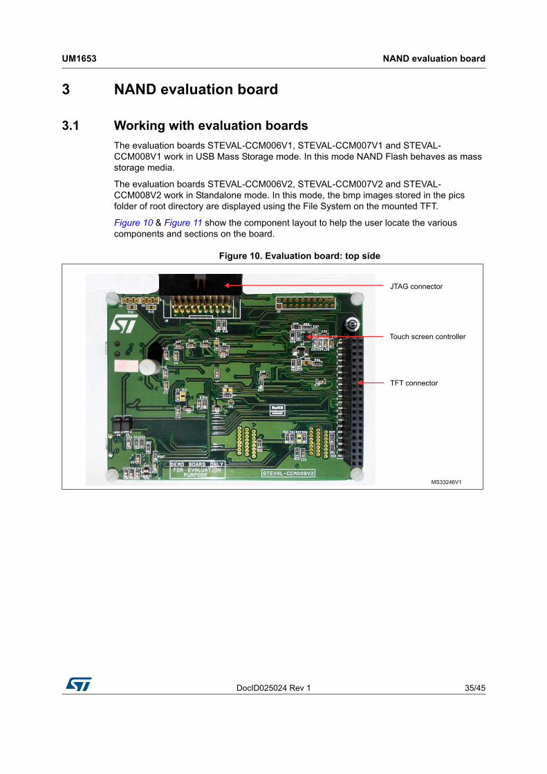
3.1 Working with evaluation boards
The evaluation boards STEVAL-CCM006V1, STEVAL-CCM007V1 and STEVAL-CCM008V1 work in USB Mass Storage mode. In this mode NAND Flash behaves as mass storage media.
The evaluation boards STEVAL-CCM006V2, STEVAL-CCM007V2 and STEVAL-CCM008V2 work in Standalone mode. In this mode, the bmp images stored in the pics folder of root directory are displayed using the File System on the mounted TFT.
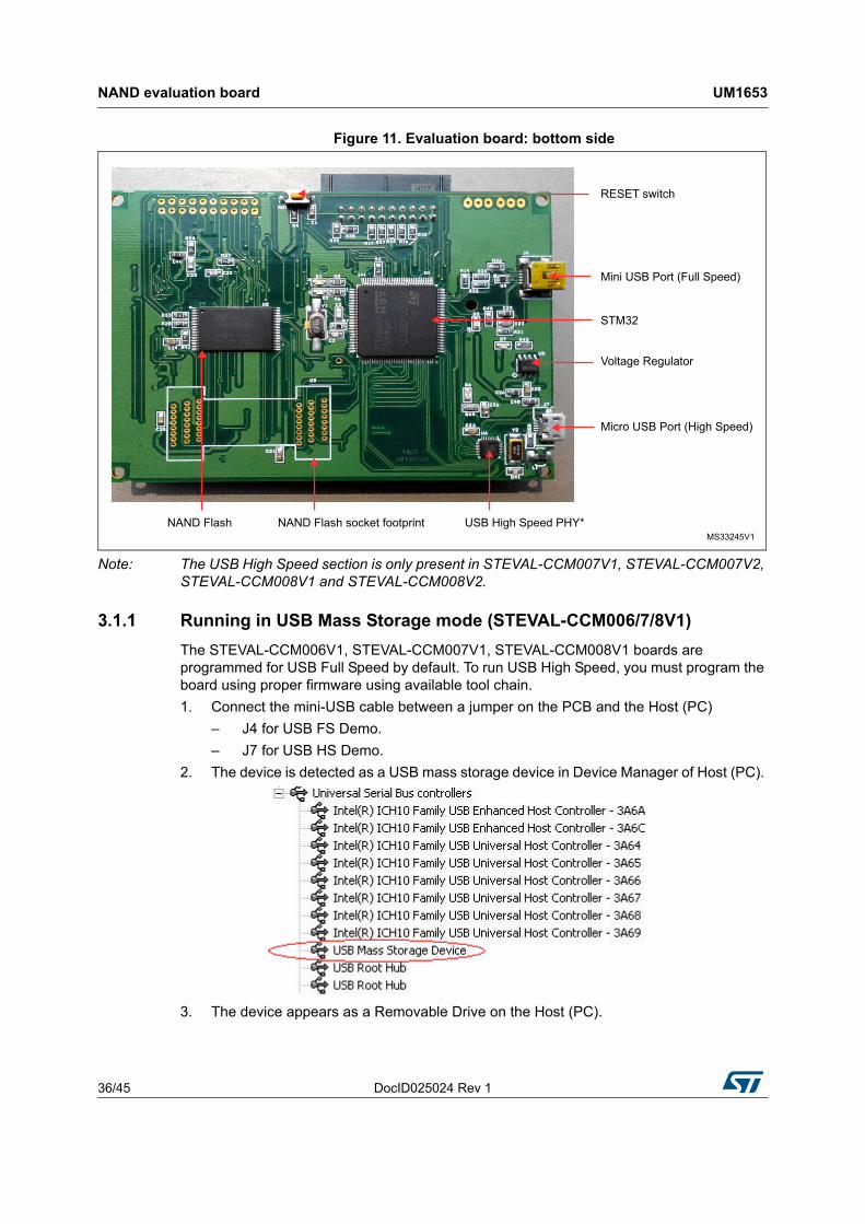
Figure 10 & Figure 11 show the component layout to help the user locate the various components and sections on the board.
Figure 10. Evaluation board: top side
MS33246V1
JTAG connector
TFT connector
Touch screen controller
NAND evaluation board UM1653
36/45 DocID025024 Rev 1
Figure 11. Evaluation board: bottom side
Note: The USB High Speed section is only present in STEVAL-CCM007V1, STEVAL-CCM007V2, STEVAL-CCM008V1 and STEVAL-CCM008V2.
3.1.1 Running in USB Mass Storage mode (STEVAL-CCM006/7/8V1)
The STEVAL-CCM006V1, STEVAL-CCM007V1, STEVAL-CCM008V1 boards are programmed for USB Full Speed by default. To run USB High Speed, you must program the board using proper firmware using available tool chain.
1. Connect the mini-USB cable between a jumper on the PCB and the Host (PC)
– J4 for USB FS Demo.
– J7 for USB HS Demo.
2. The device is detected as a USB mass storage device in Device Manager of Host (PC).
3. The device appears as a Removable Drive on the Host (PC).
MS33245V1
RESET switch
Mini USB Port (Full Speed)
Voltage Regulator
NAND Flash
Micro USB Port (High Speed)
USB High Speed PHY*NAND Flash socket footprint
STM32
DocID025024 Rev 1 37/45
UM1653 NAND evaluation board
44
4. This drive can be used as Mass Storage Media.
3.1.2 Running in Standalone mode (STEVAL-CCM006/7/8V2)
The STEVAL-CCM006V2, STEVAL-CCM007V2, STEVAL-CCM008V2 boards run in Standalone mode.
1. By default TFT is mounted on J6.
2. Connect mini-USB cable between J4 on the PCB and the Host (PC).
3. The bmp images stored in the "pics" folder of root directory are displayed on the TFT.
Figure 12. Demo running in Standalone mode
NAND evaluation board UM1653
38/45 DocID025024 Rev 1
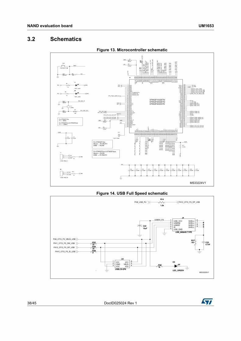
3.2 Schematics
Figure 13. Microcontroller schematic
Figure 14. USB Full Speed schematic
VCAP
PH0_OSC_IN
PH1_OSC_OUT
3V3
NRST
3V3
VCAP
VCAP
GND
3V3
GND
3V3
GND
3V3
3V3
GND
GND
GND
3V3
PE3
PB8
PE2
PB9
GND
PB
5_O
TG_H
S_U
LPI_
D7 3V
3
GN
D
3V3
PA3_
OTG
_HS
_ULP
I_D
0
3V3
PH0_OSC_IN
PB
0_O
TG_H
S_U
LPI_
D1
PH1_OSC_OUT
PA10_OTG_FS_ID_USB
GND
PE2
PB
1_O
TG_H
S_U
LPI_
D2
PC0_OTG_HS_ULPI_STP
PA13_JTAG_JTMS
PA11_OTG_FS_DM_USB
PG8_USB_PU
GN
D
3V3
PB8
3V3
PA
15_J
TAG
_JTD
I
PA12_OTG_FS_DP_USB
PB9
PA14
_JTA
G_J
TCK
PB13_OTG_HS_ULPI_D63V
3
PD
0_FS
MC
_D2
3V3PE3
PD
1_FS
MC
_D3
PB12_OTG_HS_ULPI_D5
PF0_FSMC_ADDR_A0
PB
7_I2
C1_
SD
A
PD14_FSMC_D0PD15_FSMC_D1
PB
6_I2
C1_
SC
L
PE
7_FS
MC
_D4
PE
10_F
SM
C_D
7
PE
9_FS
MC
_D6
PE
8_FS
MC
_D5
PD
5_FS
MC
_NW
E
PD11_FSMC_ADDR_A16
PE
11_F
SM
C_D
8
PD12_FSMC_ADDR_A17
PE
14_F
SM
C_D
11P
E13
_FS
MC
_D10
PE
12_F
SM
C_D
9
PD8_FSMC_D13
PE
15_F
SM
C_D
12
PD10_FSMC_D15PD9_FSMC_D14
PD
4_FS
MC
_NO
E
PB
10_O
TG_H
S_U
LPI_
D3
NRST
PC3_OTG_HS_ULPI_NXT
GN
D
GND
GN
D
3V3
GND
GND
PC2_OTG_HS_ULPI_DIR
PB
3_JT
AG
_JTD
OP
B4_
JTA
G_J
NTR
ST
3V3
3V3
PA9_OTG_FS_VBUS_USB
PB
11_O
TG_H
S_U
LPI_
D4
PA5_
OTG
_HS
_ULP
I_C
K
GN
D 3V3
PG
10_F
SM
C_N
E3
GN
D
GN
D
PG7_FSMC_INT3
PG
14_T
SC
RE
EN
_IN
T
PG6_FSMC_INT2
PD
6_FS
MC
_NW
AIT
PD
7_FS
MC
_NC
E2P
G9_
FSM
C_N
CE3
GN
D
For STM32F10xxMount --- R1,R8,R11DNM --- R3,R9
For STM32F2xxx & STM32F4xxxMount --- R3,R9DNM --- R1,R8,R11
For STM32F10xxY1----- 8MHz
For STM32F2xxx & STM32F4xxxY1------ 25MHz
STM32F103ZET6/ STM32F205ZET6/ STM32F405ZGT6
U1U1
PB14 75
PB13 74
PB12 73
VD
D_1
72V
CA
P_1
71P
B11
70P
B10
69P
E15
68P
E14
67P
E13
66P
E12
65P
E11
64P
E10
63V
DD
_762
VS
S_7
61P
E960
PE8
59P
E758
PG
157
PE43
PE54
PE65
VBAT6
PC13-TAMPER-RTC7
PC14-OSC32_IN8
PC15-OSC32_OUT9
PF010
PF111
PF212
PF313
PF515 PF414
PE21
PE32
PF719
VSS_516
PC228
VDD_517
PF618
PF820
PF921
PF1022
OSC_IN23
OSC_OUT24
NRST25
PC026
PC127
PC329
VDD_1230
VSSA31
VREF+32
VDDA33
PA0_WKUP34
PA135
PA236
PA3
37
VS
S_4
38
VD
D_4
39
PA4
40
PA5
41
PA6
42
PA7
43
PG
056
PF1
555
PF1
454
PF1
353
VD
D_6
52V
SS
_651
PF1
149
PB
2-B
OO
T148
PF1
250
PB1
47P
B046
PC
545
PC
444
PB15 76PD8 77PD9 78PD10 79PD11 80PD12 81PD13 82VSS_8 83VDD_8 84PD14 85PD15 86PG2 87PG3 88PG4 89PG5 90PG6 91PG7 92PG8 93VSS_9 94VDD_9 95PC6 96PC7 97PC8 98PC9 99PA8 100PA9 101PA10 102PA11 103PA12 104PA13 105VCAP_2 106VSS_2 107VDD_2 108
PA14
109
PA15
110
PC
1011
1P
C11
112
PC
1211
3P
D0
114
PD
111
5P
D2
116
PD
311
7P
D4
118
PD
511
9V
SS
_10
120
VD
D_1
012
1P
D6
122
PD
712
3P
G9
124
PG
1012
5P
G11
126
PG
1212
7P
G13
128
PG
1412
9V
SS
_11
130
VD
D_1
113
1P
G15
132
PB3
133
PB4
134
PB5
135
PB6
136
PB7
137
PB8
139
PB9
140
BO
OT0
138
PE0
141
PE1
142
VD
D_3
143
VD
D_S
A14
4
R1
0 Ohm0
R6
1K
C14100nFF
C12100nFF
C320pF
C13100nFF
1K
Y125MHz
C1100nF
C10100nFF
R7
390
R410KR
C8100nFF
C220pF
TP1
TEST POINT
1
J2
CONN TRBLK 3
J2
3
123
C7100nFF
R1010KR1010K
C16100nFF
R8
0 Ohm
D2
TEST_LED2
D2
C52.2uF
R9
0 Ohm
R110 Ohm
R3
0 Ohm
C42.2uF
C11100nFF
R5
1K
C15100nFF
R210KR210K
R13
1K
J1
CONN TRBLK 3
123
D1
TEST_LED1
SW1
PUSH BUTTONN
C17100nFF
C6100nFF
C9100nFF
MS33224V1
MS33225V1
USB5V_FS
PA11_OTG_FS_DM_USB
PA12_OTG_FS_DP_USB
PA12_OTG_FS_DP_USB
PA9_OTG_FS_VBUS_USB
PA10_OTG_FS_ID_USB
PG8_USB_PU
C2210uFC2210uF
J4
USB_MINIA/B TYPE
J4
USB_MINIA/B TYPE
USB_VCC1
USBDM2
USBDP3
USB_GND5
SHELL 6
SHELL 7
SHELL 8
ID4 SHELL 9
R3222R3222
R14
1.5k
R14
1.5k
C234.7nFC234.7nF
U4
USBLC6-2P6
U4
USBLC6-2P6I/O2 4VBUS 5I/O1 6I/O11
GND2
I/O23
R311MR311M
D3
LED_GREEN
D3
LED_GREEN
R3422R3422R360R360
R401kR401k
DocID025024 Rev 1 39/45
UM1653 NAND evaluation board
44
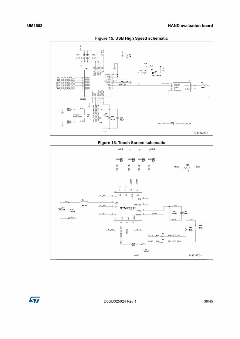
Figure 15. USB High Speed schematic
Figure 16. Touch Screen schematic
3V3_
HS
XTAL1
XTAL2
USB5V_HSPB12_OTG_HS_ULPI_D5
XTA
L1
PA3_OTG_HS_ULPI_D0 PB0_OTG_HS_ULPI_D1
XTA
L2
PC
2_O
TG_H
S_U
LPI_
DIR
PC
0_O
TG_H
S_U
LPI_
STP
PB1_OTG_HS_ULPI_D2
PA5_
OTG
_HS
_ULP
I_C
K
PC
3_O
TG_H
S_U
LPI_
NXT
PB13_OTG_HS_ULPI_D6PB5_OTG_HS_ULPI_D7
PB10_OTG_HS_ULPI_D3PB11_OTG_HS_ULPI_D4
3V3 3V3_HS
C43
0.1uF
C43
0.1uF
R520
R520
D6
LED_GREEN
D6
LED_GREEN
C42
0.1uF
C42
0.1uF
C27
0.1uF
C27
0.1uF
C36
4.7uF
C36
4.7uF
C28
0.1uF
C28
0.1uF
R47 820R47 820
C30
0.1uF
C30
0.1uF
L1
BEAD
L1
BEAD
C4133pFC4133pF
C29
0.1uF
C29
0.1uF
Y224MHzY224MHz
C444.7uFC444.7uF
R44 1KR44 1K
R501MR501M
C46
4.7uF
C46
4.7uFC4533pFC4533pF
U6
USB3300
U6
USB3300
RBIAS 32
RE
G_E
N31
VD
D3.
330
VD
DA
1.8
29
XI
28X
O27
VD
D1.
826
VD
D3.
325
GND 1
GND 2
CPEN 3
VBUS 4
ID 5
VD
D3.
36
DP 7
STP
13
CLK
OU
T14
VD
D1.
815
VD
D3.
316
GNDPAD 33
RE
SET
9
DATA717 DATA618 DATA519 DATA420 DATA321 DATA222 DATA123 DATA024
DIR
12N
XT11
EXTVBUS 10
DM 8
R4310KR4310K
R46 12KR46 12K J7J7
USB_VCC1
USBDM2
USBDP3
USB_GND5
SHELL 6
SHELL 7ID4
MS33226V1
MS33227V1
SDAT
PB6_I2C1_SCL
3V3PB7_I2C1_SDA
3V3
AGND
AGND
AGND
3V3
TSC_YD
SDAT
TSC
_YU
TSC
_XR
TSC
_YD
TSC
_XL
AGND
AG
ND
AG
ND
TSC_XR
SCLK
TSC_YU
PG
14_T
SC
RE
EN
_IN
T
TSC_XL
AG
ND
3V3AGND
SCLK
GNDAGND
R5322
R5322
C371uFC371uF
R494.7KR494.7K
R5410kR5410k
R57
0
R57
0
U7
STMPE811
U7
STMPE811
Y-
1
INT
2
A0
3
SC
LK4
SDAT 5
VCC 6
DATA_IN 7
IN0 8
IN1
9
GN
D10
IN2
11
IN3
12
X+13
VIO14
Y+15
X-16C4010uFC4010uF
C47100nFC47100nF
C312pFC312pF
C38100nFC38100nF C39
100nFC39100nF
C342pFC342pF
L2
BEAD
L2
BEAD
R5122
R5122
C332pFC332pF
R484.7KR484.7K
C322pFC322pF
NAND evaluation board UM1653
40/45 DocID025024 Rev 1
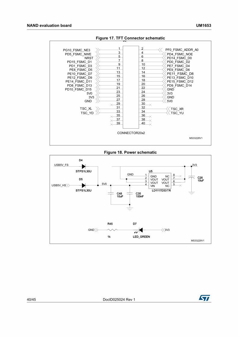
Figure 17. TFT Connector schematic
Figure 18. Power schematic
MS33228V1
PD4_FSMC_NOE
PE7_FSMC_D4
GND
PD9_FSMC_D14PE14_FSMC_D11
TSC_XR
PF0_FSMC_ADDR_A0
PE11_FSMC_D8PE8_FSMC_D5
PD10_FSMC_D15
GND
PE12_FSMC_D9
TSC_YU
PD0_FSMC_D2
TSC_YD
3V3
PE15_FSMC_D12
PD5_FSMC_NWE
PE9_FSMC_D6PD1_FSMC_D3
3V3
GNDPD8_FSMC_D13
5V0
PD14_FSMC_D0
PG10_FSMC_NE3
NRST
PE13_FSMC_D10PE10_FSMC_D7
TSC_XL
5V0
PD15_FSMC_D1
J6
CONNECTOR20x2
J6
13579
111315171921232527293133
246810121416182022242628303234
35 3637 3839 40
MS33229V1
USB5V_FS 3V3
GND
5V0
GND 3V3
USB5V_HS
D4
STPS1L30U
D4
STPS1L30U
C35100nFC35100nF
D7
LED_GREEN
D7
LED_GREEN
R45
1k
R45
1k
U5
LD1117D33TR
U5
LD1117D33TRVIN4 NC 5VOUT 6
GND1
VOUT2
VOUT3 VOUT 7NC 8C2610uFC2610uF
C4810uFC4810uF
D5
STPS1L30U
D5
STPS1L30U
DocID025024 Rev 1 41/45
UM1653 NAND evaluation board
44
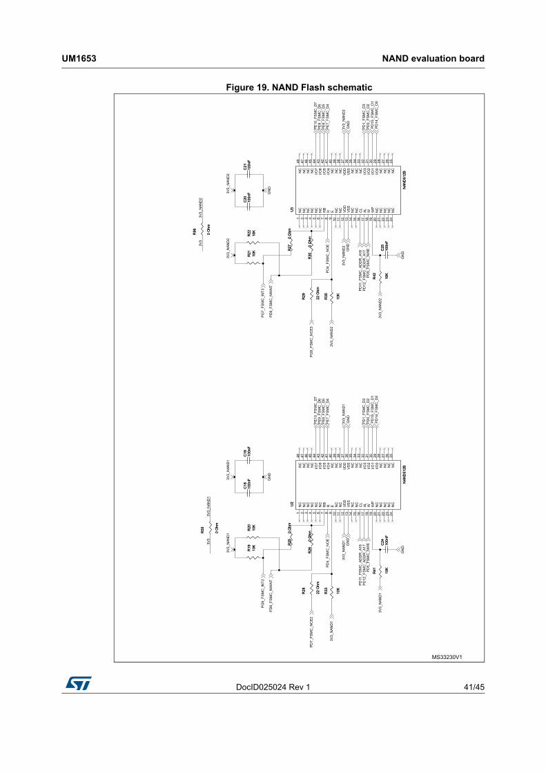
Figure 19. NAND Flash schematic
MS33230V1
3V3_
NAN
D1
3V3
3V3_
NAN
D2
3V3
PD
14_F
SM
C_D
0P
D15
_FS
MC
_D1
PD
0_FS
MC
_D2
PD
1_FS
MC
_D3
PE
7_FS
MC
_D4
PE
8_FS
MC
_D5
PE
9_FS
MC
_D6
PE
10_F
SM
C_D
7
PD
11_F
SM
C_A
DD
R_A
16P
D12
_FS
MC
_AD
DR
_A17
PD
5_FS
MC
_NW
E
PD
4_FS
MC
_NO
E3V
3_N
AND
1
GN
DG
ND
3V3_
NAN
D1
3V3_
NAN
D1
3V3_
NAN
D1
GN
D
GN
D
3V3_
NAN
D1
PD
6_FS
MC
_NW
AIT
PG
6_FS
MC
_IN
T2
3V3_
NAN
D1
PE
10_F
SM
C_D
7
PD
5_FS
MC
_NW
E
3V3_
NAN
D2
3V3_
NAN
D2
GN
D
PD
4_FS
MC
_NO
E
GN
D
GN
D
3V3_
NAN
D2
PD
14_F
SM
C_D
0
GN
D
PD
15_F
SM
C_D
1
3V3_
NAN
D2
3V3_
NAN
D2
PD
0_FS
MC
_D2
PD
11_F
SM
C_A
DD
R_A
16P
D1_
FSM
C_D
3P
D12
_FS
MC
_AD
DR
_A17
3V3_
NAN
D2
PD
6_FS
MC
_NW
AIT
PE
7_FS
MC
_D4
PE
8_FS
MC
_D5
PE
9_FS
MC
_D6
PG
7_FS
MC
_IN
T3
PD
7_FS
MC
_NC
E2P
G9_
FSM
C_N
CE3
R56
0 O
hm
R56
0 O
hm
U3
NAN
D51
2B
U3
NAN
D51
2B
NC
1
NC
2
NC
3
NC
4
NC
5
NC
6
RB
7
R8
E9
NC
10
NC
11
VDD
12
VSS
13
NC
14
NC
15
CL
16
AL17
W18
WP
19
NC
20
NC
21
NC
22
NC
23
NC
24N
C25
NC
26N
C27
NC
28I/O
029
I/O1
30I/O
231
I/O3
32N
C33
NC
34N
C35
VSS
36VD
D37
NC
38N
C39
NC
40I/O
441
I/O5
42I/O
643
I/O7
44N
C45
NC
46N
C47
NC
48
C25
100n
FC
2510
0nF
R22
10K
R22
10K
C18
100n
FC
1810
0nF
R41
10K
R41
10K
R28
22 O
hm
R28
22 O
hm
R20
10K
R20
10K
C19
100n
FC
1910
0nF
R29
22 O
hm
R29
22 O
hm
R30
0 O
hmR
300
Ohm
C21
100n
FC
2110
0nF
U2
NAN
D51
2B
U2
NAN
D51
2B
NC
1
NC
2
NC
3
NC
4
NC
5
NC
6
RB
7
R8
E9
NC
10
NC
11
VDD
12
VSS
13
NC
14
NC
15
CL
16
AL17
W18
WP
19
NC
20
NC
21
NC
22
NC
23
NC
24N
C25
NC
26N
C27
NC
28I/O
029
I/O1
30I/O
231
I/O3
32N
C33
NC
34N
C35
VSS
36VD
D37
NC
38N
C39
NC
40I/O
441
I/O5
42I/O
643
I/O7
44N
C45
NC
46N
C47
NC
48
R35
10K
R35
10K
C24
100n
FC
2410
0nF
R27
0 O
hmR
270
Ohm
C20
100n
FC
2010
0nF
R42
10K
R42
10K
R21
10K
R21
10K
R33
10K
R33
10K
R55
0 O
hm
R55
0 O
hm
R19
10K
R19
10K
R26
0 O
hmR
260
Ohm
R25
0 O
hmR
250
Ohm
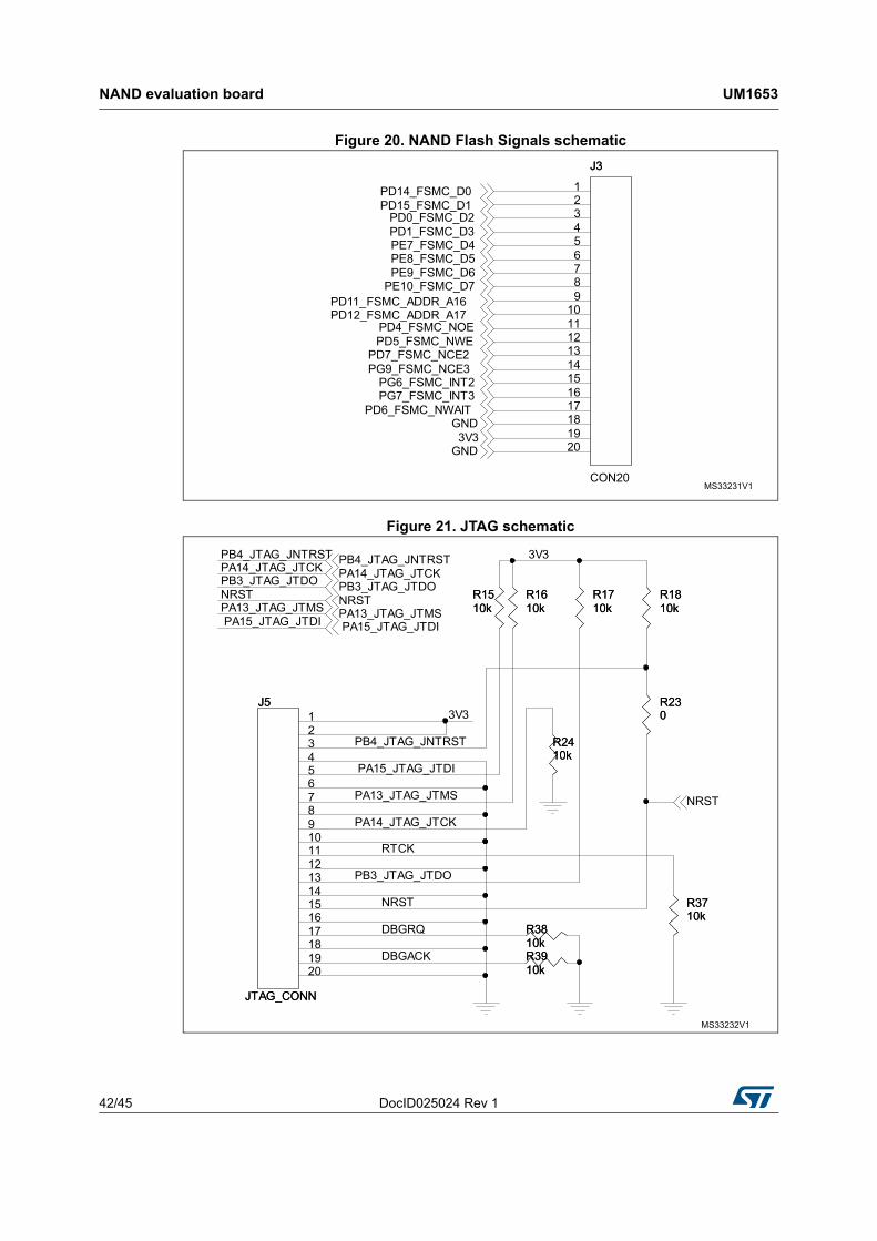
NAND evaluation board UM1653
42/45 DocID025024 Rev 1
Figure 20. NAND Flash Signals schematic
Figure 21. JTAG schematic
MS33231V1
PD15_FSMC_D1PD0_FSMC_D2PD1_FSMC_D3
PD5_FSMC_NWE
PD12_FSMC_ADDR_A17PD11_FSMC_ADDR_A16
PD4_FSMC_NOE
PE10_FSMC_D7
PE7_FSMC_D4PE8_FSMC_D5PE9_FSMC_D6
PD14_FSMC_D0
PD7_FSMC_NCE2
PD6_FSMC_NWAIT
PG6_FSMC_INT2PG9_FSMC_NCE3
PG7_FSMC_INT3
GND3V3
GND
J3
CON20
J3
123456789
1011121314151617181920
MS33232V1
3V3
PB3_JTAG_JTDO
PA13_JTAG_JTMS
PB3_JTAG_JTDOPA14_JTAG_JTCKPB4_JTAG_JNTRST
PA15_JTAG_JTDI
NRST
DBGRQ
RTCK
DBGACK
PA13_JTAG_JTMS
PA15_JTAG_JTDI
PB4_JTAG_JNTRST
3V3
NRST
PA14_JTAG_JTCK
PB3_JTAG_JTDOPA14_JTAG_JTCKPB4_JTAG_JNTRST
PA13_JTAG_JTMSNRST
PA15_JTAG_JTDI
NRST
R1810kR1810k
R1710kR1710k
R3910kR3910k
R230R230
R1610kR1610k
R3810kR3810k
R1510kR1510k
R2410kR2410k
R3710kR3710k
J5
JTAG_CONN
J5
JTAG_CONN
1234567891011121314151617181920
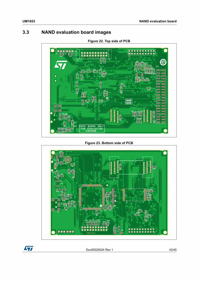
DocID025024 Rev 1 43/45
UM1653 NAND evaluation board
44
3.3 NAND evaluation board images
Figure 22. Top side of PCB
Figure 23. Bottom side of PCB
Revision history UM1653
44/45 DocID025024 Rev 1
4 Revision history
Table 58. Document revision history
Date Revision Changes
28-Nov-2013 1 Initial release.
DocID025024 Rev 1 45/45
UM1653
45
Please Read Carefully:
Information in this document is provided solely in connection with ST products. STMicroelectronics NV and its subsidiaries (“ST”) reserve theright to make changes, corrections, modifications or improvements, to this document, and the products and services described herein at anytime, without notice.
All ST products are sold pursuant to ST’s terms and conditions of sale.
Purchasers are solely responsible for the choice, selection and use of the ST products and services described herein, and ST assumes noliability whatsoever relating to the choice, selection or use of the ST products and services described herein.
No license, express or implied, by estoppel or otherwise, to any intellectual property rights is granted under this document. If any part of thisdocument refers to any third party products or services it shall not be deemed a license grant by ST for the use of such third party productsor services, or any intellectual property contained therein or considered as a warranty covering the use in any manner whatsoever of suchthird party products or services or any intellectual property contained therein.
UNLESS OTHERWISE SET FORTH IN ST’S TERMS AND CONDITIONS OF SALE ST DISCLAIMS ANY EXPRESS OR IMPLIEDWARRANTY WITH RESPECT TO THE USE AND/OR SALE OF ST PRODUCTS INCLUDING WITHOUT LIMITATION IMPLIEDWARRANTIES OF MERCHANTABILITY, FITNESS FOR A PARTICULAR PURPOSE (AND THEIR EQUIVALENTS UNDER THE LAWSOF ANY JURISDICTION), OR INFRINGEMENT OF ANY PATENT, COPYRIGHT OR OTHER INTELLECTUAL PROPERTY RIGHT.
ST PRODUCTS ARE NOT DESIGNED OR AUTHORIZED FOR USE IN: (A) SAFETY CRITICAL APPLICATIONS SUCH AS LIFESUPPORTING, ACTIVE IMPLANTED DEVICES OR SYSTEMS WITH PRODUCT FUNCTIONAL SAFETY REQUIREMENTS; (B)AERONAUTIC APPLICATIONS; (C) AUTOMOTIVE APPLICATIONS OR ENVIRONMENTS, AND/OR (D) AEROSPACE APPLICATIONSOR ENVIRONMENTS. WHERE ST PRODUCTS ARE NOT DESIGNED FOR SUCH USE, THE PURCHASER SHALL USE PRODUCTS ATPURCHASER’S SOLE RISK, EVEN IF ST HAS BEEN INFORMED IN WRITING OF SUCH USAGE, UNLESS A PRODUCT ISEXPRESSLY DESIGNATED BY ST AS BEING INTENDED FOR “AUTOMOTIVE, AUTOMOTIVE SAFETY OR MEDICAL” INDUSTRYDOMAINS ACCORDING TO ST PRODUCT DESIGN SPECIFICATIONS. PRODUCTS FORMALLY ESCC, QML OR JAN QUALIFIED AREDEEMED SUITABLE FOR USE IN AEROSPACE BY THE CORRESPONDING GOVERNMENTAL AGENCY.
Resale of ST products with provisions different from the statements and/or technical features set forth in this document shall immediately voidany warranty granted by ST for the ST product or service described herein and shall not create or extend in any manner whatsoever, anyliability of ST.
ST and the ST logo are trademarks or registered trademarks of ST in various countries.Information in this document supersedes and replaces all information previously supplied.
The ST logo is a registered trademark of STMicroelectronics. All other names are the property of their respective owners.
© 2013 STMicroelectronics - All rights reserved
STMicroelectronics group of companies
Australia - Belgium - Brazil - Canada - China - Czech Republic - Finland - France - Germany - Hong Kong - India - Israel - Italy - Japan - Malaysia - Malta - Morocco - Philippines - Singapore - Spain - Sweden - Switzerland - United Kingdom - United States of America
www.st.com