Embed Size (px)
Citation preview
NanoScience and Technology
Umberto Celano Editor
Electrical Atomic Force Microscopy for Nanoelectronics
NanoScience and Technology
Series Editors
Phaedon Avouris, IBM Research – Thomas J. Watson Research,Yorktown Heights, NY, USABharat Bhushan, Mechanical and Aerospace Engineering, The OhioState University, Columbus, OH, USADieter Bimberg, Center of NanoPhotonics, Technical University of Berlin,Berlin, GermanyCun-Zheng Ning, Electrical, Computer, and Energy Engineering,Arizona State University, Tempe, AZ, USAKlaus von Klitzing, Max Planck Institute for Solid State Research, Stuttgart,Baden-Württemberg, GermanyRoland Wiesendanger, Department of Physics, University of Hamburg,Hamburg, Germany

The series NanoScience and Technology is focused on the fascinating nano-world,mesoscopic physics, analysis with atomic resolution, nano and quantum-effectdevices, nanomechanics and atomic-scale processes. All the basic aspects andtechnology-oriented developments in this emerging discipline are covered bycomprehensive and timely books. The series constitutes a survey of the relevantspecial topics, which are presented by leading experts in the field. These books willappeal to researchers, engineers, and advanced students.
More information about this series at http://www.springer.com/series/3705
EditorUmberto CelanoIMECLeuven, Belgium
ISSN 1434-4904 ISSN 2197-7127 (electronic)NanoScience and TechnologyISBN 978-3-030-15611-4 ISBN 978-3-030-15612-1 (eBook)https://doi.org/10.1007/978-3-030-15612-1
© Springer Nature Switzerland AG 2019This work is subject to copyright. All rights are reserved by the Publisher, whether the whole or partof the material is concerned, specifically the rights of translation, reprinting, reuse of illustrations,recitation, broadcasting, reproduction on microfilms or in any other physical way, and transmissionor information storage and retrieval, electronic adaptation, computer software, or by similar or dissimilarmethodology now known or hereafter developed.The use of general descriptive names, registered names, trademarks, service marks, etc. in thispublication does not imply, even in the absence of a specific statement, that such names are exempt fromthe relevant protective laws and regulations and therefore free for general use.The publisher, the authors and the editors are safe to assume that the advice and information in thisbook are believed to be true and accurate at the date of publication. Neither the publisher nor theauthors or the editors give a warranty, expressed or implied, with respect to the material containedherein or for any errors or omissions that may have been made. The publisher remains neutral with regardto jurisdictional claims in published maps and institutional affiliations.
This Springer imprint is published by the registered company Springer Nature Switzerland AGThe registered company address is: Gewerbestrasse 11, 6330 Cham, Switzerland
Contents
1 The Atomic Force Microscopy for Nanoelectronics . . . . . . . . . . . . . 1Umberto Celano1.1 Introduction . . . . . . . . . . . . . . . . . . . . . . . . . . . . . . . . . . . . . . 11.2 Atomic Force Microscopy: The Swiss-Knife
of Nanoelectronics . . . . . . . . . . . . . . . . . . . . . . . . . . . . . . . . . 31.3 Introduction to Atomic Force Microscopy . . . . . . . . . . . . . . . . 7
1.3.1 Basic Operating Principles . . . . . . . . . . . . . . . . . . . . . 71.3.2 To Touch, or Not To Touch, That Is the Question . . . . 101.3.3 Mechanisms of Contrast Formation . . . . . . . . . . . . . . . 121.3.4 Effective Voltage Drop, Phantom Force, and Biasing
Schemes . . . . . . . . . . . . . . . . . . . . . . . . . . . . . . . . . . 181.4 Emerging Nanoelectronics Devices and Metrology
Challenges . . . . . . . . . . . . . . . . . . . . . . . . . . . . . . . . . . . . . . . 191.4.1 Device Scaling: An Increasingly Difficult
Miniaturization Landscape . . . . . . . . . . . . . . . . . . . . . 201.4.2 New Devices Based on New Physics . . . . . . . . . . . . . . 21
1.5 Present Status and Future Applications . . . . . . . . . . . . . . . . . . . 22References . . . . . . . . . . . . . . . . . . . . . . . . . . . . . . . . . . . . . . . . . . . . 24
2 Conductive AFM for Nanoscale Analysis of High-k DielectricMetal Oxides . . . . . . . . . . . . . . . . . . . . . . . . . . . . . . . . . . . . . . . . . . 29Christian Rodenbücher, Marcin Wojtyniak and Kristof Szot2.1 The C-AFM Technique . . . . . . . . . . . . . . . . . . . . . . . . . . . . . . 30
2.1.1 AFM in Contact Mode with Conducting Tips . . . . . . . 302.1.2 C-AFM Modes . . . . . . . . . . . . . . . . . . . . . . . . . . . . . . 322.1.3 Electronics . . . . . . . . . . . . . . . . . . . . . . . . . . . . . . . . . 332.1.4 Analysis of the Tip Sample Interaction: Energy
Barriers . . . . . . . . . . . . . . . . . . . . . . . . . . . . . . . . . . . 37
v
2.1.5 Requirements for Sample Preparation—The Roleof Adsorbates . . . . . . . . . . . . . . . . . . . . . . . . . . . . . . . 39
2.1.6 C-AFM with Atomic Resolution . . . . . . . . . . . . . . . . . 402.2 Basics of High-k Dielectrics . . . . . . . . . . . . . . . . . . . . . . . . . . 42
2.2.1 Scaling Limits and Challenges in SemiconductorTechnology . . . . . . . . . . . . . . . . . . . . . . . . . . . . . . . . 42
2.2.2 Technologically Relevant Metal Oxideswith High k . . . . . . . . . . . . . . . . . . . . . . . . . . . . . . . . 43
2.2.3 Synthesis of Metal Oxides . . . . . . . . . . . . . . . . . . . . . 442.3 Local Analysis of Electronic Transport Properties in Metal
Oxide Thin Films . . . . . . . . . . . . . . . . . . . . . . . . . . . . . . . . . . 462.3.1 Variation of Nanoscale Conductivity Seen
by Nanoelectrodes . . . . . . . . . . . . . . . . . . . . . . . . . . . 462.3.2 Localized Nature of Leakage Current . . . . . . . . . . . . . 462.3.3 Correlation of the Localized Conductivity
with the Surface Potential . . . . . . . . . . . . . . . . . . . . . . 492.3.4 Tuning the Conductivity by Thermal Annealing . . . . . . 512.3.5 Confinement of Conductivity at Surfaces and
Interfaces . . . . . . . . . . . . . . . . . . . . . . . . . . . . . . . . . . 532.4 Influence of Extended Defects on the Local Conductivity
of Single Crystals . . . . . . . . . . . . . . . . . . . . . . . . . . . . . . . . . . 552.4.1 Current Channelling Along Dislocations . . . . . . . . . . . 552.4.2 Analysis of Bulk Conductivity by the Cleaving
Method . . . . . . . . . . . . . . . . . . . . . . . . . . . . . . . . . . . 562.4.3 Ferroelectric Domain Walls as Conducting Paths . . . . . 57
2.5 Manipulation of the Conductivity by C-AFM . . . . . . . . . . . . . . 602.5.1 Tip-Induced Memristive Switching of Single
Dislocations in SrTiO3 . . . . . . . . . . . . . . . . . . . . . . . . 602.5.2 Creation of Conducting Nanowires on LAO/STO
Structures . . . . . . . . . . . . . . . . . . . . . . . . . . . . . . . . . 622.5.3 Electrical Nanopatterning of Oxide Surfaces . . . . . . . . 63
References . . . . . . . . . . . . . . . . . . . . . . . . . . . . . . . . . . . . . . . . . . . . 66
3 Mapping Conductance and Carrier Distributions in ConfinedThree-Dimensional Transistor Structures . . . . . . . . . . . . . . . . . . . . 71Andreas Schulze, Pierre Eyben, Jay Mody, Kristof Paredis,Lennaert Wouters, Umberto Celano and Wilfried Vandervorst3.1 Introduction: The Fundamentals of SSRM . . . . . . . . . . . . . . . . 72
3.1.1 Basic Principles . . . . . . . . . . . . . . . . . . . . . . . . . . . . . 723.1.2 Physics of the Nanoscale SSRM Contact . . . . . . . . . . . 743.1.3 Quantification . . . . . . . . . . . . . . . . . . . . . . . . . . . . . . 783.1.4 Practical Aspects . . . . . . . . . . . . . . . . . . . . . . . . . . . . 803.1.5 Application to Planar Transistor Technologies . . . . . . . 83
vi Contents
3.2 SSRM Applied to 3D Transistor Architectures . . . . . . . . . . . . . 833.2.1 CMOS Scaling and the Advent of 3D Devices . . . . . . . 843.2.2 Revisiting Dopant Metrology Requirements . . . . . . . . . 853.2.3 Understanding Dopant Incorporation and Activation
in 3D Structures . . . . . . . . . . . . . . . . . . . . . . . . . . . . . 863.2.4 Tomographic Carrier Mapping . . . . . . . . . . . . . . . . . . 913.2.5 Outsmarting Parasitic Resistances: Fast Fourier
Transform-SSRM . . . . . . . . . . . . . . . . . . . . . . . . . . . . 953.2.6 Toward Holistic Transistor Metrology: Combining
TEM and SSRM . . . . . . . . . . . . . . . . . . . . . . . . . . . . 1003.3 Summary . . . . . . . . . . . . . . . . . . . . . . . . . . . . . . . . . . . . . . . . 102References . . . . . . . . . . . . . . . . . . . . . . . . . . . . . . . . . . . . . . . . . . . . 103
4 Scanning Capacitance Microscopy for Two-Dimensional CarrierProfiling of Semiconductor Devices . . . . . . . . . . . . . . . . . . . . . . . . . 107Jay Mody and Jochonia Nxumalo4.1 Working Principle of Scanning Capacitance Microscopy . . . . . . 1074.2 Applications of Scanning Capacitance Microscopy . . . . . . . . . . 110
4.2.1 Effect of Hot Carrier Stress on Device Junctions . . . . . 1104.2.2 Root Cause Analysis for Pin Leakage . . . . . . . . . . . . . 1174.2.3 Junction Profiling of Ge Photodetector Structures
Using Scanning Capacitance Microscopy andElectron Holography . . . . . . . . . . . . . . . . . . . . . . . . . 127
4.2.4 Innovative Use of FA Techniques to Resolve JunctionScaling Issues at Advanced Technology Nodes . . . . . . 135
4.3 Summary . . . . . . . . . . . . . . . . . . . . . . . . . . . . . . . . . . . . . . . . 141References . . . . . . . . . . . . . . . . . . . . . . . . . . . . . . . . . . . . . . . . . . . . 141
5 Oxidation and Thermal Scanning Probe Lithographyfor High-Resolution Nanopatterning and Nanodevices . . . . . . . . . . 143Yu Kyoung Ryu and Armin Wolfgang Knoll5.1 Introduction . . . . . . . . . . . . . . . . . . . . . . . . . . . . . . . . . . . . . . 1435.2 Oxidation Scanning Probe Lithography: Direct Chemical
Modification at the Nanoscale . . . . . . . . . . . . . . . . . . . . . . . . . 1455.2.1 Mechanism and Growth Kinetics. Oxidation
Parameters and Operation Modes . . . . . . . . . . . . . . . . 1455.2.2 Materials Modified by Oxidation Scanning Probe
Lithography . . . . . . . . . . . . . . . . . . . . . . . . . . . . . . . . 1515.3 Thermal Scanning Probe Lithography: Fast Turnaround
Nanofabrication in Ambient Conditions Combining ThermalProbes and Focused Lasers . . . . . . . . . . . . . . . . . . . . . . . . . . . 158
5.4 Conclusion. Strengths and Limitations of SPL . . . . . . . . . . . . . 161References . . . . . . . . . . . . . . . . . . . . . . . . . . . . . . . . . . . . . . . . . . . . 163
Contents vii
6 Characterizing Ferroelectricity with an Atomic ForceMicroscopy: An All-Around Technique . . . . . . . . . . . . . . . . . . . . . 173Simon Martin, Brice Gautier, Nicolas Baboux, Alexei Gruverman,Adrian Carretero-Genevrier, Martí Gich and Andres Gomez6.1 Introduction . . . . . . . . . . . . . . . . . . . . . . . . . . . . . . . . . . . . . . 1746.2 Piezoresponse Force Microscopy as a Domain Imaging
Technique . . . . . . . . . . . . . . . . . . . . . . . . . . . . . . . . . . . . . . . 1746.2.1 Principles of Imaging Ferroelectric Domains . . . . . . . . 1746.2.2 The Converse Piezoelectric Effect as Imaging
Technique . . . . . . . . . . . . . . . . . . . . . . . . . . . . . . . . . 1756.2.3 Piezoresponse as a Quantitative Technique . . . . . . . . . 1776.2.4 Practical Aspects for Doing PFM . . . . . . . . . . . . . . . . 179
6.3 The Nano-PUND Technique . . . . . . . . . . . . . . . . . . . . . . . . . . 1826.3.1 The Principle of PUND Measurement . . . . . . . . . . . . . 1836.3.2 Nano-PUND: PUND Method Implemented
in an AFM. . . . . . . . . . . . . . . . . . . . . . . . . . . . . . . . . 1846.3.3 Examples and Applications of Nano-PUND
Measurements . . . . . . . . . . . . . . . . . . . . . . . . . . . . . . 1856.3.4 Future Developments of Nano-PUND Technique . . . . . 187
6.4 Direct Piezoelectric Force Microscopy as a QuantitativeTool . . . . . . . . . . . . . . . . . . . . . . . . . . . . . . . . . . . . . . . . . . . . 1886.4.1 Principles of DPFM . . . . . . . . . . . . . . . . . . . . . . . . . . 1886.4.2 Quantitative Data in DPFM . . . . . . . . . . . . . . . . . . . . 1926.4.3 Practical How-to Guide for Imaging with DPFM . . . . . 193
6.5 Applications of Nanoscale Ferroelectric Characterizationinto Semiconductors . . . . . . . . . . . . . . . . . . . . . . . . . . . . . . . . 1966.5.1 Solar Cells . . . . . . . . . . . . . . . . . . . . . . . . . . . . . . . . . 1966.5.2 Sensors . . . . . . . . . . . . . . . . . . . . . . . . . . . . . . . . . . . 1986.5.3 Negative Capacitance . . . . . . . . . . . . . . . . . . . . . . . . . 198
References . . . . . . . . . . . . . . . . . . . . . . . . . . . . . . . . . . . . . . . . . . . . 200
7 Electrical AFM for the Analysis of Resistive Switching . . . . . . . . . 205Stefano Brivio, Jacopo Frascaroli and Min Hwan Lee7.1 Introduction to Resistive Switching . . . . . . . . . . . . . . . . . . . . . 205
7.1.1 Devices and Applications . . . . . . . . . . . . . . . . . . . . . . 2067.1.2 Physics of Resistive Switching . . . . . . . . . . . . . . . . . . 207
7.2 AFM Experimental Setup for Resistive SwitchingCharacterization . . . . . . . . . . . . . . . . . . . . . . . . . . . . . . . . . . . 2097.2.1 Advantages of AFM . . . . . . . . . . . . . . . . . . . . . . . . . . 2097.2.2 Contact AFM Techniques . . . . . . . . . . . . . . . . . . . . . . 2097.2.3 Non-contact AFM Techniques . . . . . . . . . . . . . . . . . . . 211
7.3 Noteworthy AFM Scientific Results . . . . . . . . . . . . . . . . . . . . . 2127.3.1 Interfacial Switching . . . . . . . . . . . . . . . . . . . . . . . . . . 213
viii Contents
7.3.2 Filamentary Switching . . . . . . . . . . . . . . . . . . . . . . . . 2147.3.3 C-AFM as a Nano-probe for Critical
Morphologies . . . . . . . . . . . . . . . . . . . . . . . . . . . . . . . 2217.4 Conclusions . . . . . . . . . . . . . . . . . . . . . . . . . . . . . . . . . . . . . . 2247.5 Perspectives . . . . . . . . . . . . . . . . . . . . . . . . . . . . . . . . . . . . . . 225References . . . . . . . . . . . . . . . . . . . . . . . . . . . . . . . . . . . . . . . . . . . . 225
8 Magnetic Force Microscopy for Magnetic Recordingand Devices . . . . . . . . . . . . . . . . . . . . . . . . . . . . . . . . . . . . . . . . . . . 231Atsufumi Hirohata, Marjan Samiepour and Marco Corbetta8.1 Introduction . . . . . . . . . . . . . . . . . . . . . . . . . . . . . . . . . . . . . . 231
8.1.1 Magnetic Imaging . . . . . . . . . . . . . . . . . . . . . . . . . . . 2328.1.2 Magnetic Force Microscopy . . . . . . . . . . . . . . . . . . . . 2338.1.3 Other SPM-Based Magnetic Microscopy . . . . . . . . . . . 234
8.2 Principles of Non-contact/Tapping Mode . . . . . . . . . . . . . . . . . 2378.2.1 Principles of Non-contact Atomic
Force Microscopy . . . . . . . . . . . . . . . . . . . . . . . . . . . 2378.2.2 Principles of Magnetic Force Microscopy . . . . . . . . . . 238
8.3 Magnetic Tips and Specifications . . . . . . . . . . . . . . . . . . . . . . . 2418.3.1 Magnetic Tips . . . . . . . . . . . . . . . . . . . . . . . . . . . . . . 2418.3.2 Improvement of Specifications . . . . . . . . . . . . . . . . . . 251
8.4 Applications for Magnetic Recording . . . . . . . . . . . . . . . . . . . . 2518.4.1 3.5-in. Floppy Disk Introduced in 1987 . . . . . . . . . . . . 2528.4.2 Zip Drive Introduced in 1994 . . . . . . . . . . . . . . . . . . . 2538.4.3 Fujitsu HDD Introduced in 2007 . . . . . . . . . . . . . . . . . 2548.4.4 Seagate HDD Introduced in 2009 . . . . . . . . . . . . . . . . 2568.4.5 Western Digital HDD Introduced in 2012 . . . . . . . . . . 2568.4.6 Seagate HDD Introduced in 2016 . . . . . . . . . . . . . . . . 2568.4.7 Outlook . . . . . . . . . . . . . . . . . . . . . . . . . . . . . . . . . . . 257
8.5 Applications for Magnetic Memories and Devices . . . . . . . . . . 2598.5.1 Magnetic Random Access Memory and Spin Random
Access Memory . . . . . . . . . . . . . . . . . . . . . . . . . . . . . 2598.5.2 Racetrack Memory . . . . . . . . . . . . . . . . . . . . . . . . . . . 2608.5.3 Magnetic Skyrmion Logics . . . . . . . . . . . . . . . . . . . . . 261
References . . . . . . . . . . . . . . . . . . . . . . . . . . . . . . . . . . . . . . . . . . . . 263
9 Space Charge at Nanoscale: Probing Injection and DynamicPhenomena Under Dark/Light Configurations by Using KPFMand C-AFM . . . . . . . . . . . . . . . . . . . . . . . . . . . . . . . . . . . . . . . . . . 267Christina Villeneuve-Faure, Kremena Makasheva, Laurent Boudouand Gilbert Teyssedre9.1 Context . . . . . . . . . . . . . . . . . . . . . . . . . . . . . . . . . . . . . . . . . 268
9.1.1 Miniaturization of Thin Dielectric Layers . . . . . . . . . . 2689.1.2 Interfaces . . . . . . . . . . . . . . . . . . . . . . . . . . . . . . . . . . 269
Contents ix
9.2 KPFM and C-AFM Measurement Under Dark and LightConfigurations . . . . . . . . . . . . . . . . . . . . . . . . . . . . . . . . . . . . 2709.2.1 Introduction to Surface Potential . . . . . . . . . . . . . . . . . 2709.2.2 Surface Potential Measurement in AM-KPFM . . . . . . . 2719.2.3 Surface Potential Measurement in FM-KPFM . . . . . . . 2749.2.4 Surface Potential Measurement in PF-KPFM . . . . . . . . 2749.2.5 Photoconductive and Photo-KPFM Modes . . . . . . . . . . 2769.2.6 KPFM Modelling . . . . . . . . . . . . . . . . . . . . . . . . . . . . 277
9.3 Local Charges Injection Mechanisms . . . . . . . . . . . . . . . . . . . . 2789.3.1 Local Injection Using Conductive AFM-Tip
and Surface Potential Measurements . . . . . . . . . . . . . . 2799.3.2 Charges Injection and Decay in Thin Dielectric
Layers . . . . . . . . . . . . . . . . . . . . . . . . . . . . . . . . . . . . 2839.4 KPFM for Space Charge Probing in Semiconductor
and Dielectric Materials . . . . . . . . . . . . . . . . . . . . . . . . . . . . . 2879.4.1 KPFM Measurements on Bias Electronic Devices:
Challenge and Bottleneck . . . . . . . . . . . . . . . . . . . . . . 2879.4.2 Methodology for Charge Density Profile
Determination from KPFM Measurements . . . . . . . . . . 2879.4.3 Applications to Dielectrics and Semiconductors . . . . . . 289
9.5 Nanoscale Opto-Electrical Characterization of Thin FilmBased Solar Cells Using KPFM and C-AFM . . . . . . . . . . . . . . 2929.5.1 Mapping Measurements . . . . . . . . . . . . . . . . . . . . . . . 2929.5.2 Localized Current-Voltage Measurements . . . . . . . . . . 293
9.6 Conclusion and Overview . . . . . . . . . . . . . . . . . . . . . . . . . . . . 295References . . . . . . . . . . . . . . . . . . . . . . . . . . . . . . . . . . . . . . . . . . . . 296
10 Conductive AFM of 2D Materials and Heterostructuresfor Nanoelectronics . . . . . . . . . . . . . . . . . . . . . . . . . . . . . . . . . . . . . 303Filippo Giannazzo, Giuseppe Greco, Fabrizio Roccaforte,Chandreswar Mahata and Mario Lanza10.1 Introduction . . . . . . . . . . . . . . . . . . . . . . . . . . . . . . . . . . . . . . 30310.2 Large Area Synthesis of Graphene, MoS2 and h-BN
for Electronics . . . . . . . . . . . . . . . . . . . . . . . . . . . . . . . . . . . . 30610.3 Overview of 2D Materials-Based Electronic Devices . . . . . . . . 310
10.3.1 Graphene FETs for High Frequency Electronics . . . . . . 31010.3.2 2D-Semiconductors FETs for Digital Electronics . . . . . 31110.3.3 Vertical Transistors Based on 2D-Materials
Heterostructures . . . . . . . . . . . . . . . . . . . . . . . . . . . . . 31310.3.4 Transistors Based on 2D Materials Heterojunctions
with Bulk Semiconductors . . . . . . . . . . . . . . . . . . . . . 315
x Contents
10.4 C-AFM Applications to 2D Material and Devices: CaseStudies . . . . . . . . . . . . . . . . . . . . . . . . . . . . . . . . . . . . . . . . . . 31910.4.1 Nanoscale Mapping of Transport Properties
in Graphene and MoS2 . . . . . . . . . . . . . . . . . . . . . . . . 31910.4.2 Vertical Current Injection Through 2D/3D or 2D/2D
Materials Heterojunctions . . . . . . . . . . . . . . . . . . . . . . 32810.4.3 Electrical Characterization of h-BN as Two
Dimensional Dielectric: Lateral Inhomogeneity,Reliability and Dielectric Breakdown. . . . . . . . . . . . . . 333
10.5 Summary . . . . . . . . . . . . . . . . . . . . . . . . . . . . . . . . . . . . . . . . 342References . . . . . . . . . . . . . . . . . . . . . . . . . . . . . . . . . . . . . . . . . . . . 343
11 Diamond Probes Technology . . . . . . . . . . . . . . . . . . . . . . . . . . . . . . 351Thomas Hantschel, Thierry Conard, Jason Kilpatrickand Graham Cross11.1 Introduction . . . . . . . . . . . . . . . . . . . . . . . . . . . . . . . . . . . . . . 35211.2 Molded Diamond Tip Probes . . . . . . . . . . . . . . . . . . . . . . . . . . 354
11.2.1 Basic Fabrication Process . . . . . . . . . . . . . . . . . . . . . . 35511.2.2 Probe Process Variations . . . . . . . . . . . . . . . . . . . . . . 35811.2.3 Fabrication Results . . . . . . . . . . . . . . . . . . . . . . . . . . . 359
11.3 Probe Characterization . . . . . . . . . . . . . . . . . . . . . . . . . . . . . . 36311.3.1 Probe Storage Considerations . . . . . . . . . . . . . . . . . . . 364
11.4 Conclusions on Molded Diamond Probes . . . . . . . . . . . . . . . . . 36811.5 Plasma Etched Single Crystal Doped Diamond Probes . . . . . . . 368
11.5.1 Manufacturing . . . . . . . . . . . . . . . . . . . . . . . . . . . . . . 36911.6 Applications . . . . . . . . . . . . . . . . . . . . . . . . . . . . . . . . . . . . . . 372
11.6.1 Scanning Tunneling Microscopy—AtomicResolution Imaging . . . . . . . . . . . . . . . . . . . . . . . . . . 373
11.6.2 Conductive Atomic Force Microscopy . . . . . . . . . . . . . 37311.6.3 Scanning Capacitance Microscopy . . . . . . . . . . . . . . . . 37411.6.4 Scanning Spreading Resistance Microscopy . . . . . . . . . 37711.6.5 Measurement of High Aspect Ratio Structures . . . . . . . 377
11.7 Conclusions and Outlook . . . . . . . . . . . . . . . . . . . . . . . . . . . . 380References . . . . . . . . . . . . . . . . . . . . . . . . . . . . . . . . . . . . . . . . . . . . 381
12 Scanning Microwave Impedance Microscopy (sMIM)in Electronic and Quantum Materials . . . . . . . . . . . . . . . . . . . . . . . 385Kurt A. Rubin, Yongliang Yang, Oskar Amster,David A. Scrymgeour and Shashank Misra12.1 Introduction . . . . . . . . . . . . . . . . . . . . . . . . . . . . . . . . . . . . . . 38512.2 Theory of Operation—sMIM . . . . . . . . . . . . . . . . . . . . . . . . . . 386
12.2.1 Working Principal of sMIM . . . . . . . . . . . . . . . . . . . . 38612.2.2 Contrast Mechanism . . . . . . . . . . . . . . . . . . . . . . . . . . 38812.2.3 Technique Benefits . . . . . . . . . . . . . . . . . . . . . . . . . . . 389
Contents xi
12.2.4 Single Electrode Measurement . . . . . . . . . . . . . . . . . . 38912.2.5 Measuring Buried Structures . . . . . . . . . . . . . . . . . . . . 38912.2.6 Monotonic with Permittivity . . . . . . . . . . . . . . . . . . . . 39112.2.7 Monotonic with Log Doping Concentration . . . . . . . . . 392
12.3 Characterization of Nanomaterials with sMIM . . . . . . . . . . . . . 39512.3.1 Dielectric Materials . . . . . . . . . . . . . . . . . . . . . . . . . . 39512.3.2 Semiconducting Materials . . . . . . . . . . . . . . . . . . . . . . 39512.3.3 2D Materials . . . . . . . . . . . . . . . . . . . . . . . . . . . . . . . 39812.3.4 Quantum Materials . . . . . . . . . . . . . . . . . . . . . . . . . . . 400
12.4 Summary and Conclusion . . . . . . . . . . . . . . . . . . . . . . . . . . . . 403References . . . . . . . . . . . . . . . . . . . . . . . . . . . . . . . . . . . . . . . . . . . . 405
xii Contents
Contributors
Oskar Amster PrimeNano, Inc., Santa Clara, CA, USA;KLA, One Technology Drive, Milpitas, CA, USA
Nicolas Baboux Institut des Nanotechnologies de Lyon, INSA de Lyon,Université de Lyon, UMR CNRS 5270, Villeurbanne, France
Laurent Boudou LAPLACE, Université de Toulouse, CNRS, UPS, INPT,Toulouse, France
Stefano Brivio CNR-IMM, Unit of Agrate Brianza, Agrate Brianza, Italy
Adrian Carretero-Genevrier Institut d’Electronique et des Systemes (IES),CNRS, Universite Montpellier, Montpellier, France
Umberto Celano IMEC, Leuven, Belgium
Thierry Conard IMEC, Leuven, Belgium
Marco Corbetta NanoScan AG, Dübendorf, Switzerland
Graham Cross Adama Innovations, CRANN, Trinity College Dublin, Dublin,Ireland;Trinity College, School of Physics, Dublin 2, Ireland
Pierre Eyben IMEC, Leuven, Belgium
Jacopo Frascaroli STMicroelectronics, Agrate Brianza, Italy
Brice Gautier Institut des Nanotechnologies de Lyon, INSA de Lyon, Universitéde Lyon, UMR CNRS 5270, Villeurbanne, France
Filippo Giannazzo Consiglio Nazionale delle Ricerche, Institute forMicroelectronics and Microsystems (CNR-IMM), Catania, Italy
Martí Gich Institut de Ciència de Materials de Barcelona (ICMAB-CSIC),Bellaterra, Spain
xiii
Andres Gomez Institut de Ciència de Materials de Barcelona (ICMAB-CSIC),Bellaterra, Spain
Giuseppe Greco Consiglio Nazionale delle Ricerche, Institute forMicroelectronics and Microsystems (CNR-IMM), Catania, Italy
Alexei Gruverman Department of Physics and Astronomy, University ofNebraska-Lincoln, Lincoln, NE, USA
Thomas Hantschel IMEC, Leuven, Belgium
Atsufumi Hirohata Department of Electronic Engineering, University of York,Heslington, York, UK
Jason Kilpatrick Conway Institute of Biomedical and Biomolecular Research,University College Dublin, Dublin, Ireland;Adama Innovations, CRANN, Trinity College Dublin, Dublin, Ireland
Armin Wolfgang Knoll IBM Research Laboratory Zurich, Zürich, Switzerland
Mario Lanza Institute of Functional Nano & Soft Materials, CollaborativeInnovation Center of the Ministry of Education, Soochow University, Suzhou,China
Min Hwan Lee Department of Mechanical Engineering, University of California—Merced, Merced, USA
Chandreswar Mahata Institute of Functional Nano & Soft Materials,Collaborative Innovation Center of the Ministry of Education, Soochow University,Suzhou, China
Kremena Makasheva LAPLACE, Université de Toulouse, CNRS, UPS, INPT,Toulouse, France
Simon Martin Institut des Nanotechnologies de Lyon, INSA de Lyon, Universitéde Lyon, UMR CNRS 5270, Villeurbanne, France
Shashank Misra Sandia National Laboratories, Albuquerque, NM, USA
Jay Mody GLOBALFOUNDRIES, Malta, NY, USA
Jochonia Nxumalo GLOBALFOUNDRIES, Malta, NY, USA
Kristof Paredis IMEC, Leuven, Belgium
Fabrizio Roccaforte Consiglio Nazionale delle Ricerche, Institute forMicroelectronics and Microsystems (CNR-IMM), Catania, Italy
Christian Rodenbücher Forschungszentrum Jülich GmbH, Peter GrünbergInstitute (PGI-7) and JARA-FIT, Jülich, Germany;Forschungszentrum Jülich GmbH, Institute of Energy and Climate Research(IEK-3), Jülich, Germany
xiv Contributors
Kurt A. Rubin PrimeNano, Inc., Santa Clara, CA, USA;KLA, One Technology Drive, Milpitas, CA, USA
Yu Kyoung Ryu Instituto de Ciencia de Materiales de Madrid, Consejo Superiorde Investigaciones Científicas (CSIC), Madrid, Spain
Marjan Samiepour Department of Electronic Engineering, University of York,Heslington, York, UK
Andreas Schulze IMEC, Leuven, Belgium;Applied Materials, Santa Clara, CA, USA
David A. Scrymgeour Sandia National Laboratories, Albuquerque, NM, USA
Kristof Szot Forschungszentrum Jülich GmbH, Peter Grünberg Institute (PGI-7)and JARA-FIT, Jülich, Germany;University of Silesia, A. Chełkowski Institute of Physics, Katowice, Poland
Gilbert Teyssedre LAPLACE, Université de Toulouse, CNRS, UPS, INPT,Toulouse, France
Wilfried Vandervorst IMEC, Leuven, Belgium;Department of Physics and Astronomy, KU Leuven, Leuven, Belgium
Christina Villeneuve-Faure LAPLACE, Université de Toulouse, CNRS, UPS,INPT, Toulouse, France
Marcin Wojtyniak University of Silesia, A. Chełkowski Institute of Physics,Katowice, Poland
Lennaert Wouters IMEC, Leuven, Belgium
Yongliang Yang PrimeNano, Inc., Santa Clara, CA, USA
Contributors xv
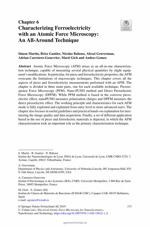
Chapter 6Characterizing Ferroelectricitywith an Atomic Force Microscopy:An All-Around Technique
Simon Martin, Brice Gautier, Nicolas Baboux, Alexei Gruverman,Adrian Carretero-Genevrier, Martí Gich and Andres Gomez
Abstract Atomic Force Microscopy (AFM) arises as an all-in-one characteriza-tion technique, capable of measuring several physical quantities by slight equip-ment’smodifications. In particular, for piezo and ferroelectricity properties, theAFMovercame the limitations of macroscopic techniques. This chapter covers all theaspects of piezo and ferroelectricity measurements performed with an AFM. Thechapter is divided in three main parts, one for each available technique: Piezore-sponse Force Microscopy (PFM), Nano-PUND method and Direct PiezoelectricForce Microscopy (DPFM). While PFM method is based in the converse piezo-electric effect, nanoPUND measures polarization charges and DPFM measures thedirect piezoelectric effect. The working principle and characteristics for each AFMmode is fully exploited and explained from entry level to more advanced users. Thechapter also focuses in useful guidelines and practical hands-on explanation for max-imizing the image quality and data acquisition. Finally, a set of different applicationbased in the use of piezo and ferroelectric materials is depicted, in which the AFMcharacterization took an important role as the primary characterization technique.
S. Martin · B. Gautier · N. BabouxInstitut des Nanotechnologies de Lyon, INSA de Lyon, Université de Lyon, UMR CNRS 5270, 7,Avenue, Capelle, 69621 Villeurbanne, France
A. GruvermanDepartment of Physics and Astronomy, University of Nebraska-Lincoln, 081 Jorgensen Hall, 855N 16th Street, Lincoln, NE 68588-0299, USA
A. Carretero-GenevrierInstitut d’Electronique et des Systemes (IES), CNRS, Universite Montpellier, 2 860 Rue de SaintPriest, 34095 Montpellier, France
M. Gich · A. Gomez (B)Institut de Ciència de Materials de Barcelona (ICMAB-CSIC), Campus UAB, 08193 Bellaterra,Spaine-mail: [email protected]
© Springer Nature Switzerland AG 2019U. Celano (ed.), Electrical Atomic Force Microscopy for Nanoelectronics,NanoScience and Technology, https://doi.org/10.1007/978-3-030-15612-1_6
173
174 S. Martin et al.
6.1 Introduction
While piezoelectric and ferroelectric materials started as laboratory rareness materi-als, during the 20th century their applications expanded from laboratory to industryand common electronic components. More recent industrial applications includetheir use as electromechanical systems, energy harvester for sensors in the Internetof Things (IoT), memory devices and as gate dielectric materials, among others. Thisbroad range of applications relies on the same key: the understanding and control atthe nanoscale of the piezoelectric effect.
In this sense, Atomic Force Microscopes have provided a platform from whichboth piezoelectricity and ferroelectricity can be studied. In this chapterwewill reviewand analyze the state-of-the-art techniques from the family AFM advanced modes.The chapter covers from the most classical approach, exploiting the converse piezo-electric effect, to novel techniques relying into the use of the direct piezoelectriceffect. More importantly, we describe not only methods to map ferroelectricity andpiezoelectricity, but also an AFM-based technique that can be used to acquire thepolarization charge density of the material, which is of special interest to capacitorsand electronic components. A set of novel and promising applications closes thechapter, to give ideas into what are the uses and implications of piezoelectricity inthe near future.
6.2 Piezoresponse Force Microscopy as a Domain ImagingTechnique
Piezoresponse Force Microscopy (PFM) is an advanced Atomic Force Microscopy(AFM) mode capable of imaging ferroelectric domains through the converse piezo-electric effect, measuring the material displacement as a function of the applied bias.In order to exploit the technique, an introduction into the imaging mechanism isprovided, followed by a hands-on step-by-step guide.
6.2.1 Principles of Imaging Ferroelectric Domains
Piezoelectricity includes two different and equivalent definitions [1]. For one side,piezoelectricity is the amount of charge density that is generated when a mechanicalstrain is applied to the material. This approach was given in the 19th century by Curiebrothers [2] while in a later time, “converse” effect was discovered. The ConversePiezoelectric Effect (CPE) is defined as the mechanical strain as a function of theapplied electric field [3]. The direct and converse piezoelectric effects are expressedby the following equations:
6 Characterizing Ferroelectricity with an Atomic Force Microscopy … 175
Pi = di jk · X jk, for direct effect (6.1)
Si = di jk · E jk, for converse effect (6.2)
where P is the polarization, X the stress, S the strain, E the electric fields and d the“piezoelectric coefficient”. In fact, since these equations are related both to vectors(polarization and electric field) and second rank tensors (stress and strain), d is arank three tensor. Since stress and strain tensors are symmetric, d consists of 18independent coefficients represented by a 3 × 6 matrix dij with i = 1–3, j = 1–6. Ifwe simplify the equation for the out-of-plane perpendicular case, the equations takethe form:
σ = d33 · F, for direct effect (6.3)
A = d33V, for converse effect (6.4)
In which σ is the surface charge density, F is the force per unit area applied by thetip to the sample in the direction perpendicular to its surface, V is the applied biasand A is the displacement. In both cases, the constant d33, is called the piezoelectricconstant, which has either units of pC/N or pm/V (1 pm/V = 1 pC/m) [3, 4]. Theconverse and direct piezoelectric effects offer two alternatives to study piezoelec-tric and ferroelectric materials. For each possibility, there exists one AFM-basedtechnique, namely Piezoresponse Force Microscopy (PFM) which is based on theconverse effect and Direct Piezoelectric Force Microscopy (DPFM), based on thedirect effect.
6.2.2 The Converse Piezoelectric Effect as ImagingTechnique
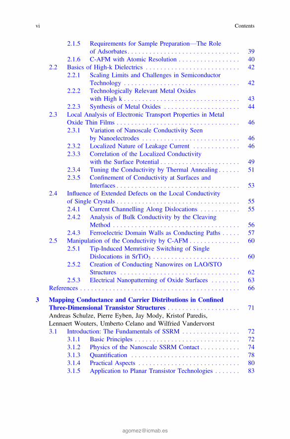
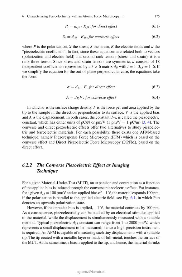
For a given Material-Under-Test (MUT), an expansion and contraction as a functionof the applied bias is induced through the converse piezoelectric effect. For instance,for a given d33 = 100 pm/V and an applied bias of+1V, thematerial expands 100 pm,if the polarization is parallel to the applied electric field, see Fig. 6.1, in which Pupdenotes an upwards polarization state.
However, if the opposite bias is applied, −1 V, the material contracts by 100 pm.As a consequence, piezoelectricity can be studied by an electrical stimulus appliedto the material, while the displacement is simultaneously measured with a suitablemethod. Typical piezoelectric d33 constant can range from 1 to 2000 pm/V, whichrepresents a small displacement to be measured; hence a high precision instrumentis required. An AFM is capable of measuring such tiny displacements with a suitabletip. The tip coated with a metallic layer or made of full-metal, touches the surface oftheMUT. At the same time, a bias is applied to the tip, and hence, thematerial shrinks
176 S. Martin et al.
Fig. 6.1 The CPE explained: without bias applied the material rests in its initial position, a For agiven positive bias applied, the material expands, b while for a negative bias, c MUT contracts
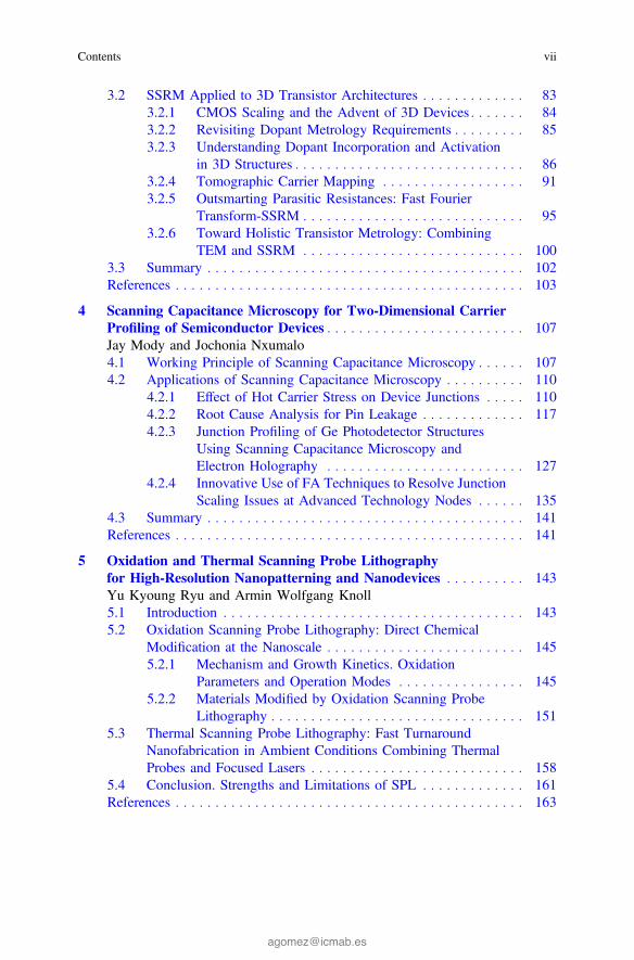
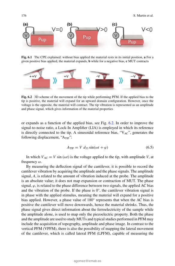
Fig. 6.2 3D scheme of the movement of the tip while performing PFM. If the applied bias to thetip is positive, the material will expand for an upward domain configuration. However, once thevoltage is the opposite, the material will contract. The tip vibration is represented as an amplitudeand phase signal, which gives information of the material properties
or expands as a function of the applied bias, see Fig. 6.2. In order to improve thesignal-to-noise ratio, a Lock-In Amplifier (LIA) is employed in which its referenceis directly connected to the tip. A sinusoidal reference bias, “VAC”, generates thefollowing displacement, “ATIP”:
ATIP = V d33 sin(ωt + ϕ) (6.5)
In which VAC = V sin (ωt) is the voltage applied to the tip, with amplitude V, atfrequency ω.
By measuring the deflection signal of the cantilever, it is possible to record thecantilever vibration by acquiring the amplitude and the phase signals. The amplitudesignal, A, is related to the amount of vibration induced at the probe. The amplitudeis an absolute value; it does not map expansion or contraction of MUT. The phasesignal, ϕ, is related to the phase difference between two signals, the applied AC biasand the vibration of the probe. If the phase is 0°, the cantilever vibration signal isin phase with the applied stimulus, meaning the material will expand for a positivebias applied. However, a phase value of 180° represents that when the AC bias ispositive the cantilever will move downwards, hence the material shrinks. Thus, thephase signal gives direct information about the ferroelectricity of the sample whilethe amplitude alone, is used to map only the piezoelectric property. Both the phaseand the amplitude are used to studyMUTs and typical studies performed in PFMmayinclude the acquisition of topography, amplitude and phase image. In contrast to thevertical PFM (VPFM), there is also the possibility of mapping the lateral movementof the cantilever, which is called lateral PFM (LPFM), capable of measuring the
6 Characterizing Ferroelectricity with an Atomic Force Microscopy … 177
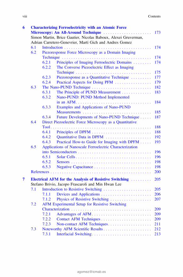
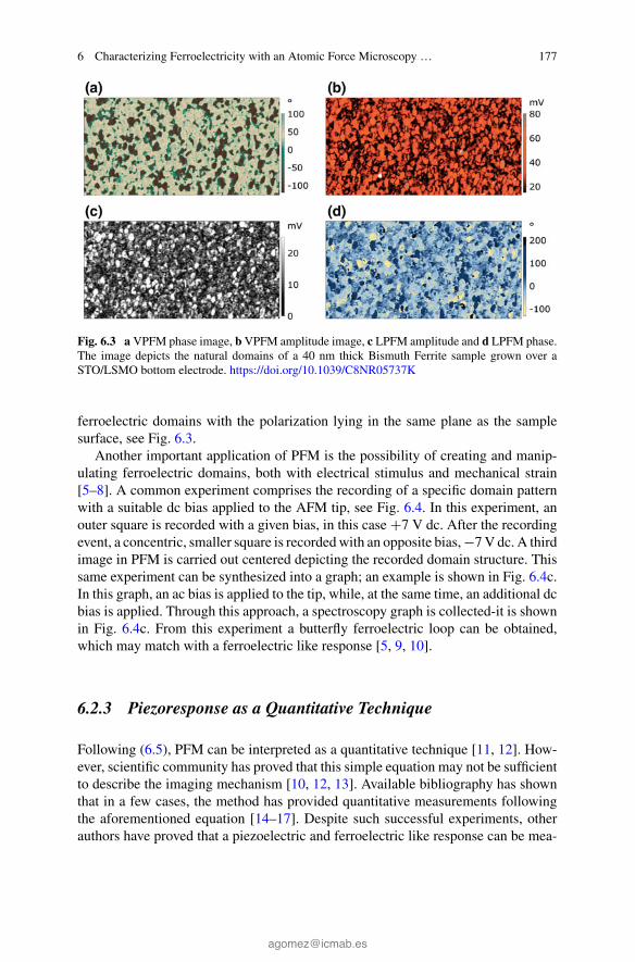
Fig. 6.3 a VPFM phase image, b VPFM amplitude image, c LPFM amplitude and d LPFM phase.The image depicts the natural domains of a 40 nm thick Bismuth Ferrite sample grown over aSTO/LSMO bottom electrode. https://doi.org/10.1039/C8NR05737K
ferroelectric domains with the polarization lying in the same plane as the samplesurface, see Fig. 6.3.
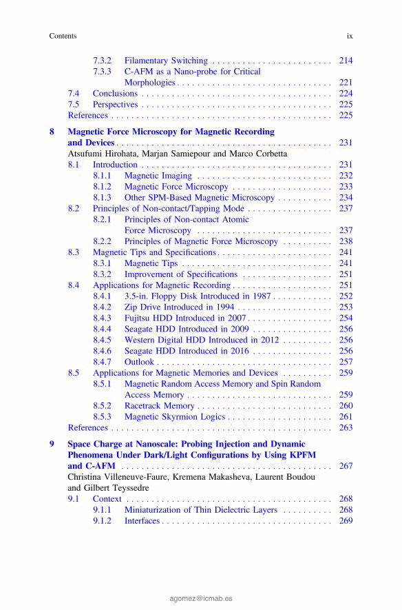
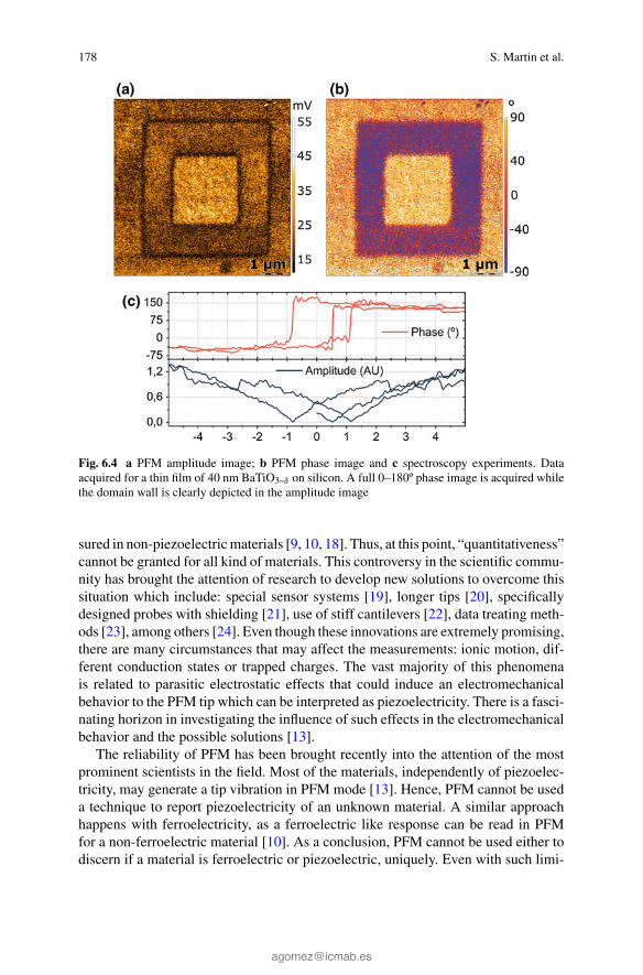
Another important application of PFM is the possibility of creating and manip-ulating ferroelectric domains, both with electrical stimulus and mechanical strain[5–8]. A common experiment comprises the recording of a specific domain patternwith a suitable dc bias applied to the AFM tip, see Fig. 6.4. In this experiment, anouter square is recorded with a given bias, in this case +7 V dc. After the recordingevent, a concentric, smaller square is recordedwith an opposite bias,−7V dc. A thirdimage in PFM is carried out centered depicting the recorded domain structure. Thissame experiment can be synthesized into a graph; an example is shown in Fig. 6.4c.In this graph, an ac bias is applied to the tip, while, at the same time, an additional dcbias is applied. Through this approach, a spectroscopy graph is collected-it is shownin Fig. 6.4c. From this experiment a butterfly ferroelectric loop can be obtained,which may match with a ferroelectric like response [5, 9, 10].
6.2.3 Piezoresponse as a Quantitative Technique
Following (6.5), PFM can be interpreted as a quantitative technique [11, 12]. How-ever, scientific community has proved that this simple equation may not be sufficientto describe the imaging mechanism [10, 12, 13]. Available bibliography has shownthat in a few cases, the method has provided quantitative measurements followingthe aforementioned equation [14–17]. Despite such successful experiments, otherauthors have proved that a piezoelectric and ferroelectric like response can be mea-
178 S. Martin et al.
Fig. 6.4 a PFM amplitude image; b PFM phase image and c spectroscopy experiments. Dataacquired for a thin film of 40 nm BaTiO3–δ on silicon. A full 0–180º phase image is acquired whilethe domain wall is clearly depicted in the amplitude image
sured in non-piezoelectricmaterials [9, 10, 18]. Thus, at this point, “quantitativeness”cannot be granted for all kind of materials. This controversy in the scientific commu-nity has brought the attention of research to develop new solutions to overcome thissituation which include: special sensor systems [19], longer tips [20], specificallydesigned probes with shielding [21], use of stiff cantilevers [22], data treating meth-ods [23], among others [24]. Even though these innovations are extremely promising,there are many circumstances that may affect the measurements: ionic motion, dif-ferent conduction states or trapped charges. The vast majority of this phenomenais related to parasitic electrostatic effects that could induce an electromechanicalbehavior to the PFM tip which can be interpreted as piezoelectricity. There is a fasci-nating horizon in investigating the influence of such effects in the electromechanicalbehavior and the possible solutions [13].
The reliability of PFM has been brought recently into the attention of the mostprominent scientists in the field. Most of the materials, independently of piezoelec-tricity, may generate a tip vibration in PFM mode [13]. Hence, PFM cannot be useda technique to report piezoelectricity of an unknown material. A similar approachhappens with ferroelectricity, as a ferroelectric like response can be read in PFMfor a non-ferroelectric material [10]. As a conclusion, PFM cannot be used either todiscern if a material is ferroelectric or piezoelectric, uniquely. Even with such limi-

6 Characterizing Ferroelectricity with an Atomic Force Microscopy … 179
tation, PFM is a uniquely and powerful domain imaging technique to report domainstructures at the nanoscale.
6.2.4 Practical Aspects for Doing PFM
This section is devoted to users that want a kick-off for their PFM measurements; inthis section we summarize all the corks and tricks of an experienced PFM user.
1.4.a. A testing platform
A known ferroelectric sample is mandatory for the users carrying out PFM mea-surements. The most common testing sample, is called “Periodically Poled LithiumNiobate” (PPLN) that can be purchased in major optical retailers or AFM compa-nies. This sample is used firstly to introduce you in PFM and acquiring your veryfirst images but also, it is employed as a troubleshooting testing platform. An alterna-tive sample may comprise a piezoelectric buzzer, commonly presented in electronicstores, polished and heated to create a natural domain structure. Both lithium niobateand the piezoelectric buzzer, which normally is composed of lead zirconate titanatematerial, are known to be piezoelectric and ferroelectric materials.
1.4.b. The probe selection
The probe is one of the most important parts for any AFM method. From all theavailable technologies, a conductive tip has to be employed. The most commonone is the Pt/Ir coated AFM probe, however the coating tends to degrade easily.Another common approach is to use full metal tips, on which wearing does notaffect its conductivity and a longer tip shank length reduces electrostatic interaction.The probe is commercialized mounted in different cantilevers, with different springconstants. The recommendation is to employ relatively stiff cantilevers, for instance,in Pt/Ir technology a common cantilever has a k = 3 N/m while, for a solid platinumtip, a common k constant of 18 N/m is found. A stiff cantilever is recommendedto provide a good tip-sample mechanical contact and reduce electrostatic effects.Since typical ferroelectric materials are hard ceramics, there is no sample plasticdeformation upon scanning. Other metallic probes may include doped single crystaldiamond tips, titanium coated tips and doped diamond coated tips.
1.4.c. The equipment
Thevastmajority ofAFMmicroscopes are equipedwith components to performPFMby feeding the probe with a suitable AC signal and routing the deflection signal intoa Lock-In Amplifier (LIA) input. However, a common modification for PFM users isto bypass the commercial electronics and feed the AC voltage signal directly to thetip with an external coaxial cable. This improves the capacitive coupling betweenthe signal cables and the AC generation that can influence the measured signals.An external lock-in amplifier can be used to overpass the equipment built-in LIA,if necessary. Other common modifications include improving the trans-impedance
180 S. Martin et al.
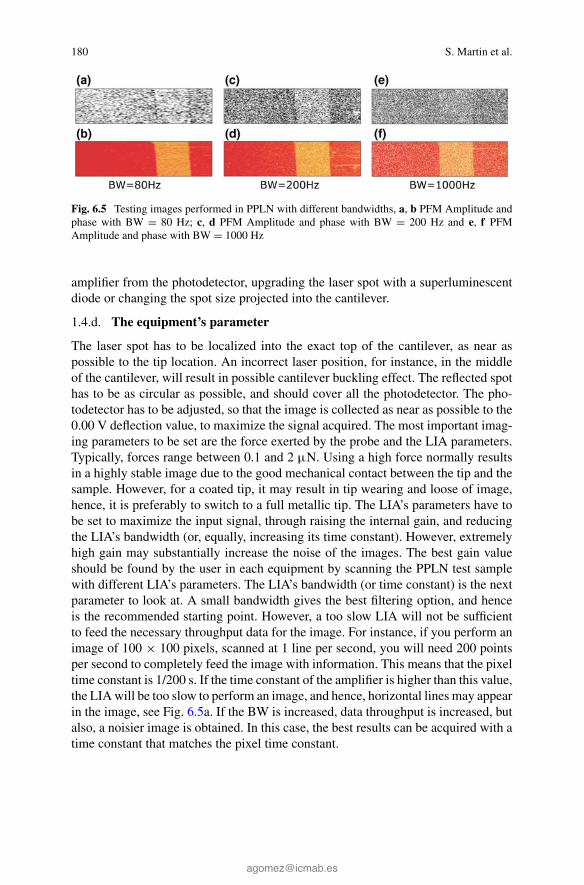
Fig. 6.5 Testing images performed in PPLN with different bandwidths, a, b PFM Amplitude andphase with BW = 80 Hz; c, d PFM Amplitude and phase with BW = 200 Hz and e, f PFMAmplitude and phase with BW = 1000 Hz
amplifier from the photodetector, upgrading the laser spot with a superluminescentdiode or changing the spot size projected into the cantilever.
1.4.d. The equipment’s parameter
The laser spot has to be localized into the exact top of the cantilever, as near aspossible to the tip location. An incorrect laser position, for instance, in the middleof the cantilever, will result in possible cantilever buckling effect. The reflected spothas to be as circular as possible, and should cover all the photodetector. The pho-todetector has to be adjusted, so that the image is collected as near as possible to the0.00 V deflection value, to maximize the signal acquired. The most important imag-ing parameters to be set are the force exerted by the probe and the LIA parameters.Typically, forces range between 0.1 and 2 μN. Using a high force normally resultsin a highly stable image due to the good mechanical contact between the tip and thesample. However, for a coated tip, it may result in tip wearing and loose of image,hence, it is preferably to switch to a full metallic tip. The LIA’s parameters have tobe set to maximize the input signal, through raising the internal gain, and reducingthe LIA’s bandwidth (or, equally, increasing its time constant). However, extremelyhigh gain may substantially increase the noise of the images. The best gain valueshould be found by the user in each equipment by scanning the PPLN test samplewith different LIA’s parameters. The LIA’s bandwidth (or time constant) is the nextparameter to look at. A small bandwidth gives the best filtering option, and henceis the recommended starting point. However, a too slow LIA will not be sufficientto feed the necessary throughput data for the image. For instance, if you perform animage of 100 × 100 pixels, scanned at 1 line per second, you will need 200 pointsper second to completely feed the image with information. This means that the pixeltime constant is 1/200 s. If the time constant of the amplifier is higher than this value,the LIAwill be too slow to perform an image, and hence, horizontal lines may appearin the image, see Fig. 6.5a. If the BW is increased, data throughput is increased, butalso, a noisier image is obtained. In this case, the best results can be acquired with atime constant that matches the pixel time constant.
6 Characterizing Ferroelectricity with an Atomic Force Microscopy … 181
1.4.e. The environment
To perform experiments in PFM, it is important to control the environmental con-ditions inside the AFM box. Typically, experiments are carried out in controlledatmospheric conditions with low humidity environment. If the AFM does not havea climate chamber, it is possible to fill the complete AFM box with compressed air,which reduces the ambient humidity to values of less than 6%. Another commonapproach is to fill the chamber with nitrogen gas to reduce the humidity further to3% and getting rid of oxygen. However, security measurements have to be taken.
1.4.f. Procedure
A step-by-step guide into acquiring PFM images is provided in the following page:
a. Place the AFM tip into the tip holder. It has to be placed as centered as possible,which is very important for thismode. Laser spot is adjusted so that it is as close aspossible to the top of the tip location-which is not the same as the very end of thecantilever. Laser photodetector is adjusted so that its value is as close as possibleto 0.00 V, to maximize the sensitivity. A coaxial cable is connected directly tothe tip-or a suitable switch to route the AC signal to the tip is configured. Sampleis mounted into a conductive plate, which is connected to the DC generator ofan AFM (typically, “sample bias” channel) with suitable silver paint. With thesample ready to scan, the box is closed and compressed air/nitrogen is filledinside. The imaging software has to be configured to acquire LIA’s “Amplitude”and “Phase” channels.
b. Once humidity is below 10%, the tip can be approached to the sample. Onceengaged, the LIA’s generator can be feed into the tip, a typical starting amplitudeis 2 VAC and frequency set to 20 kHz. The LIA’s is configured with an aggressivetime constant, for instance 10 ms (100 Hz BW) for images at 1 lines per second.The gain parameter is maximized so that the signal is not clipped. With theseparameters, an image can be acquired. If natural domains can be seen, you canuse this frame to adjust the time constant and gain parameters of the LIA. Acommon trick at this point is to reduce the scan speed, which enables the use ofeven higher LIA’s time constant, hence a better filtering is achieved.
c. If at this point no stable signal can be obtained in the frames, you can increasethe AC voltage applied to the tip up to the maximum value. In case the image isnot stable, check the topography channel to see if topography image is obtained.In case the piezoelectric signal is not measured, you can change the appliedAC frequency to the contact resonance frequency-which increases the signal-to-noise ratio. To do so, a frequency sweep over a range of 20–200 kHz is typicallyemployed to look for the resonance peak. The resonance peak should be foundbetween the first and second resonance of the cantilever,measured in air. Once thepeak is found, the frequency can be changed to match such resonance frequency.After all these steps are carried out and there is still no signal, we can concludethat either natural domains are not present or they are too small to be imaged. Ifyou can see the domains, you can set the Dual-Resonance Amplitude Trackingfeature in your AFM, whenever such option is available.
182 S. Martin et al.
d. The next step is to prove if you can create a domain configuration into the MUT.To do so, you can start by performing a spectroscopy experiment-similar to onethat is found in Fig. 6.4c.With the same starting parameters described in b a curvefor “Amplitude and “Phase” channels versus applied DC bias can be run. Thetypical sweep goes from 0 to +6VDC, then from +6VDC to −6VDC to back +6VDC. The sweep rate can be set to ranges from 5–20 V/s with data throughputsof 80–500 points per second. If in the spectroscopy window you cannot obtain asimilar graph like shown in Fig. 6.4c, you can switch to the resonance frequencyas for the case c, and repeat the curves. If you are able to reproduce a butterfly-likeferroelectric loops you should be able to record a suitable domain configuration.
e. Recording the domain configuration is a multistep process. A typical domainrecording is found in Fig. 6.3 consisting of 2 consequent squares. For one side, abigger image, typical of 6 × 6 μm is performed with 0 VAC and applying a DCbias to the tip. From spectroscopy data obtained at d you can, approximately,calculate the necessary voltage to record the domains. Too much voltage, and thelayer may undergo breakdown conditions, leading to the appearance of undesiredtopographic features. The voltage has to be high enough to record the domain,but not too high to break the sample. After the big square is recorded, a smallerone is created concentric to the bigger one. Typically sizes are 4 × 4 μm or 2 ×2 μm. These image sizes are enough for most common AFM to avoid driftingoccurring in smaller images. After the two consequent squares are recorded, it istime to read the domain structure. To do so, a bigger than initial image has to beemployed, for instance, 10 × 10 μm, to read the domain configuration followingb.
6.3 The Nano-PUND Technique
Nano-PUND is a technique introduced in 2017 [25] which has been developed to beused as a complement to PFM analysis or as an alternative to it. PFM has becomethe most widely used technique to assess ferroelectricity at the nanoscale but suffersfrom numerous possible artifacts. Indeed, electrostatic [26] and electrochemical [27]contributions are responsible for parasitic andmisleading PFMsignals in e.g. leaky oroxygen vacancies-richmaterials [18, 28–30]. It has become obvious that PFM imagesand loops could be obtained on non-ferroelectric materials, highlighting the need fora complementary technique which could assess ferroelectricity in a more reliableway in such cases. PUND technique, already implemented on several hundreds ofmicrons large electrodes, has thus been adapted at the nanoscale to detect andmeasureremnant polarization with an atomic force microscope.
6 Characterizing Ferroelectricity with an Atomic Force Microscopy … 183
6.3.1 The Principle of PUND Measurement
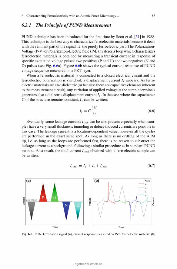
PUND technique has been introduced for the first time by Scott et al. [31] in 1988.This technique is the best way to characterize ferroelectric materials because it dealswith the remnant part of the signal i.e. the purely ferroelectric part. The Polarization-Voltage (P-V) or Polarization-Electric field (P-E) hysteresis loopwhich characterizesferroelectric materials is obtained by measuring a transient current in response ofspecific excitation voltage pulses: two positives (P and U) and two negatives (N andD) pulses (see Fig. 6.6a). Figure 6.6b shows the typical current response of PUNDvoltage sequence measured on a PZT layer.
When a ferroelectric material is connected to a closed electrical circuit and theferroelectric polarization is switched, a displacement current I f appears. As ferro-electricmaterials are also dielectric (or because there are capacitive elements inherentto the measurement circuit), any variation of applied voltage at the sample terminalsgenerates also a dielectric displacement current Iε. In the case where the capacitanceC of the structure remains constant, Iε can be written:
Iε = C∂V
∂t(6.6)
Eventually, some leakage currents I leak can be also present especially when sam-ples have a very small thickness: tunneling or defect-induced currents are possible inthis case. The leakage current is a location-dependent value, however all the cyclesare performed in the exact same spot. As long as there is no drifting of the AFMtip, i.e. as long as the loops are performed fast, there is no reason to substract theleakage current as a background, following a similar procedure as in standard PUNDmethod. As a result, the total current I total obtained with a ferroelectric sample canbe written:
Itotal = I f + Iε + Ileak (6.7)
Fig. 6.6 PUND excitation signal (a), current response measured on PZT ferroelectric material (b)
184 S. Martin et al.
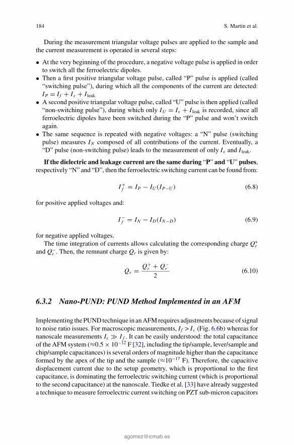
During the measurement triangular voltage pulses are applied to the sample andthe current measurement is operated in several steps:
• At the very beginning of the procedure, a negative voltage pulse is applied in orderto switch all the ferroelectric dipoles.
• Then a first positive triangular voltage pulse, called “P” pulse is applied (called“switching pulse”), during which all the components of the current are detected:IP = I f + Iε + I leak.
• A second positive triangular voltage pulse, called “U” pulse is then applied (called“non-switching pulse”), during which only IU = I ε + I leak is recorded, since allferroelectric dipoles have been switched during the “P” pulse and won’t switchagain.
• The same sequence is repeated with negative voltages: a “N” pulse (switchingpulse) measures IN composed of all contributions of the current. Eventually, a“D” pulse (non-switching pulse) leads to the measurement of only Iε and I leak.
If the dielectric and leakage current are the same during “P” and “U” pulses,respectively “N” and “D”, then the ferroelectric switching current can be found from:
I+f = IP − IU (IP−U ) (6.8)
for positive applied voltages and:
I−f = IN − ID(IN−D) (6.9)
for negative applied voltages.The time integration of currents allows calculating the corresponding charge Q+
rand Q−
r . Then, the remnant charge Qr is given by:
Qr = Q+r + Q−
r
2(6.10)
6.3.2 Nano-PUND: PUND Method Implemented in an AFM
Implementing thePUNDtechnique in anAFMrequires adjustments because of signalto noise ratio issues. For macroscopic measurements, I f > Iε (Fig. 6.6b) whereas fornanoscale measurements Iε � I f . It can be easily understood: the total capacitanceof the AFM system (≈0.5× 10⁻¹² F [32], including the tip/sample, lever/sample andchip/sample capacitances) is several orders of magnitude higher than the capacitanceformed by the apex of the tip and the sample (≈10−17 F). Therefore, the capacitivedisplacement current due to the setup geometry, which is proportional to the firstcapacitance, is dominating the ferroelectric switching current (which is proportionalto the second capacitance) at the nanoscale. Tiedke et al. [33] have already suggesteda technique to measure ferroelectric current switching on PZT sub-micron capacitors
6 Characterizing Ferroelectricity with an Atomic Force Microscopy … 185
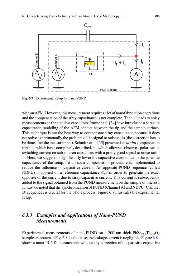
Fig. 6.7 Experimental setup for nano-PUND
with anAFM.However, thismeasurement requires a lot of nanofabrication operationsand the compensation of the stray capacitance is not complete. Then, it leads to noisymeasurements on the smallest capacitors. Prume et al. [34] have introduced a parasiticcapacitance modeling of the AFM contact between the tip and the sample surface.This technique is not the best way to compensate stray capacitance because it doesnot solve experimentally the problem of the signal to noise ratio (the correction has tobe done after themeasurement). Schmitz et al. [35] presented an in situ compensationmethod,which is not completely described, butwhich allows to observe a polarizationswitching current on sub-micron capacitors with a pretty good signal to noise ratio.
Here, we suggest to significantly lower the capacitive current due to the parasiticcapacitance of the setup. To do so, a compensation procedure is implemented toreduce the influence of capacitive current. An opposite PUND sequence (calledNDPU) is applied on a reference capacitance Cref in order to generate the exactopposite of the current due to stray capacitive current. This current is subsequentlyadded to the signal obtained from the PUNDmeasurement on the sample of interest.It must be noted that the synchronization of PUND (Channel A) and NDPU (ChannelB) sequences is crucial for the whole process. Figure 6.7 illustrates the experimentalsetup.
6.3.3 Examples and Applications of Nano-PUNDMeasurements
Experimental measurements of nano-PUND on a 200 nm thick PbZr0.52Ti0.48O3
sample are shown inFig. 6.8. In this case, the leakage current is negligible. Figure 6.8ashows a nano-PUNDmeasurement without any correction of the parasitic capacitive
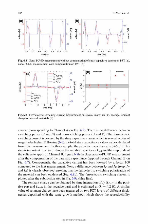
186 S. Martin et al.
Fig. 6.8 Nano-PUND measurement without compensation of stray capacitive current on PZT (a),nano-PUND measurement with compensation on PZT (b)
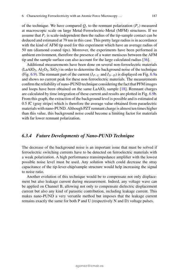
Fig. 6.9 Ferroelectric switching current measurement on several materials (a), average remnantcharge on several materials (b)
current (corresponding to Channel A on Fig. 6.7). There is no difference betweenswitching pulses (P and N) and non-switching pulses (U and D). The ferroelectricswitching current is covered by the stray capacitive current which is several orders ofmagnitudes higher. Following (6.6), the total stray capacitancevalue canbe calculatedfrom this measurement. In this example, the parasitic capacitance is 0.65 pF. Thisstep is important in order to choose the suitable capacitance Cref and the amplitude ofthe voltage to apply on Channel B. Figure 6.8b displays a nano-PUNDmeasurementafter the compensation of the parasitic capacitance (applied through Channel B onFig. 6.7). Consequently, the capacitive current has been lowered by a factor 100compared to the first measurement. Now, a difference between IP and IU (resp. INand ID) is clearly observed, proving that the ferroelectric switching polarization ofthe material can been evidenced (Fig. 6.8b). The ferroelectric switching current isplotted after the subtraction step in Fig. 6.9a (blue line).
The remnant charge can be obtained by time integration of I f (IP−U in the posi-tive part and IN−D in the negative part) and is estimated at Qr = 4.2 fC. A similarvalue of remnant charge have been measured on two PZT layers of different thick-nesses deposited with the same growth method, which shows the reproducibility
6 Characterizing Ferroelectricity with an Atomic Force Microscopy … 187
of the technique. We have compared Qr to the remnant polarization (Pr) measuredat macroscopic scale on large Metal-Ferroelectric-Metal (MFM) structures. If weassume that Pr is scale-independent then the radius of the tip-sample contact can bededuced and estimated at 79 nm in this case. This pretty large radius is in accordancewith the kind of AFM tip used for this experiment which have an average radius of50 nm (diamond coated tips). Moreover, the experiments have been performed inambient environment, therefore the presence of a water meniscus between the AFMtip and the sample surface can also account for the large calculated radius [36].
Additional measurements have been done on several non-ferroelectric materials(LaAlO3, Al2O3, SiO2) in order to determine the background noise of the technique(Fig. 6.9). The remnant part of the current (IP−U and IN−D) is displayed on Fig. 6.9aand shows no current peak for these non-ferroelectric materials. The measurementsconfirm the reliability of nano-PUND technique considering the fact that PFM imagesand loops have been obtained on the same LaAlO3 sample [18]. Remnant chargesare calculated by time integration of these current and results are plotted in Fig. 6.9b.From this graph, the extraction of the background level is possible and is estimated at0.5 fC (gray stripe) which is therefore the average value obtained from paraelectricmaterials with nano-PUND.Although PZT remnant charge is almost ten times higherthan this value, this background noise could become a limiting factor for materialswith far lower remnant polarization.
6.3.4 Future Developments of Nano-PUND Technique
The decrease of the background noise is an important issue that must be solved ifferroelectric switching currents have to be detected on ferroelectric materials witha weak polarization. A high performance transimpedance amplifier with the lowestpossible noise level must be used. Any solution which could decrease the straycapacitance of the tip-lever-chip/sample structure would help increasing the signalto noise ratio.
Another evolution of this technique would be to compensate not only displace-ment but also leakage current during measurement. Indeed, any voltage wave canbe applied on Channel B, allowing not only to compensate dielectric displacementcurrent but also any kind of parasitic contribution, including leakage current. Thismakes nano-PUND a very versatile method but imposes that the leakage currentremains exactly the same for both P and U (respectively N and D) voltage pulses.

188 S. Martin et al.
6.4 Direct Piezoelectric Force Microscopy as a QuantitativeTool
In part one of this chapter,we analyzed how theCPE is used as an imagingmechanismto map ferroelectricity in MUTs. In this part we will introduce and analyze how thedirect piezoelectric effect provides a different and complementary view to the PFMinformation.
6.4.1 Principles of DPFM
The direct piezoelectric effect is used in DPFM as imaging mechanism by applying amechanical stress and measuring the generated charge [3, 37]. The piezo-generatedcharge measuring protocol is not trivial, and it is not until 2017 in which the fea-sibility and implementation of DPFM was demonstrated [37]. The main limitationfor this implementation arises from a technologically point of view as an appro-priate operational amplifier (OA) was not available. As an example, if a suitablepiezoelectric sample, with d33 value of 50 pC/N, is strained with 100 μN force, thegenerated charge is 50 × 10−4 pC, which indeed, it’s an extremely tiny amount ofcharge for the existing sensing electronics. The direct piezoelectric effect is schema-tized in Fig. 6.10, for a given ferroelectric material with an upwards out-of-planepolarization, a pulling force generated a negative charge (see Fig. 6.10a). Reversingthe applied force, inverses the generated charge sign (see Fig. 6.10b) [3, 38].
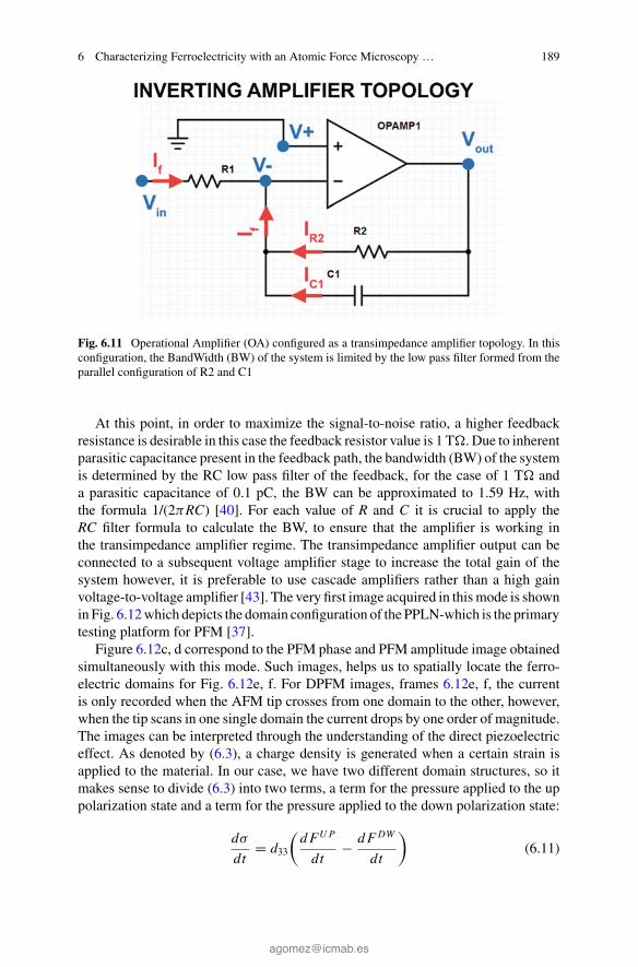
A correct selection of appropriate electronics to measure such charge is crucial.Typical OAs have a leakage current in the order of pA range, hence, the generatedcharge is likely to be absorbed by the leakage current of the OA [39–41]. In this con-figuration, the OA is configured like a transimpedance amplifier, in which the circuitacts as a current-to-voltage converter, with a current gain matching the feedbackresistor of the circuit, R2, see Fig. 6.11 [42].
Fig. 6.10 Explanation of the direct piezoelectric effect phenomena. If a force pulls a material andexpands it, a negative charge is built up on top of its surface as in (a). However, if the force is appliedin the opposite direction, the generated charge sign inverses as in (b)
6 Characterizing Ferroelectricity with an Atomic Force Microscopy … 189
Fig. 6.11 Operational Amplifier (OA) configured as a transimpedance amplifier topology. In thisconfiguration, the BandWidth (BW) of the system is limited by the low pass filter formed from theparallel configuration of R2 and C1
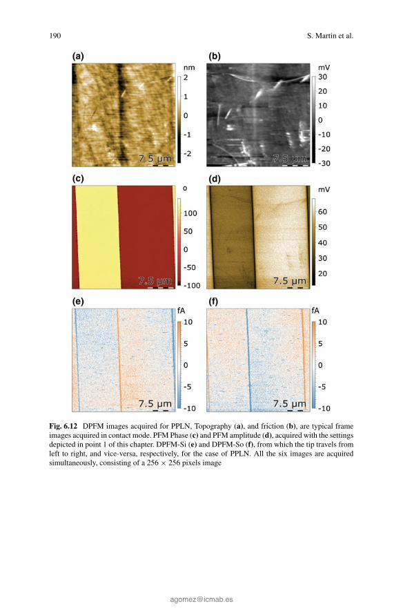
At this point, in order to maximize the signal-to-noise ratio, a higher feedbackresistance is desirable in this case the feedback resistor value is 1 T�. Due to inherentparasitic capacitance present in the feedback path, the bandwidth (BW) of the systemis determined by the RC low pass filter of the feedback, for the case of 1 T� anda parasitic capacitance of 0.1 pC, the BW can be approximated to 1.59 Hz, withthe formula 1/(2πRC) [40]. For each value of R and C it is crucial to apply theRC filter formula to calculate the BW, to ensure that the amplifier is working inthe transimpedance amplifier regime. The transimpedance amplifier output can beconnected to a subsequent voltage amplifier stage to increase the total gain of thesystem however, it is preferable to use cascade amplifiers rather than a high gainvoltage-to-voltage amplifier [43]. The very first image acquired in thismode is shownin Fig. 6.12which depicts the domain configuration of the PPLN-which is the primarytesting platform for PFM [37].
Figure 6.12c, d correspond to the PFM phase and PFM amplitude image obtainedsimultaneously with this mode. Such images, helps us to spatially locate the ferro-electric domains for Fig. 6.12e, f. For DPFM images, frames 6.12e, f, the currentis only recorded when the AFM tip crosses from one domain to the other, however,when the tip scans in one single domain the current drops by one order of magnitude.The images can be interpreted through the understanding of the direct piezoelectriceffect. As denoted by (6.3), a charge density is generated when a certain strain isapplied to the material. In our case, we have two different domain structures, so itmakes sense to divide (6.3) into two terms, a term for the pressure applied to the uppolarization state and a term for the pressure applied to the down polarization state:
dσ
dt= d33
(dFUP
dt− dFDW
dt
)(6.11)
190 S. Martin et al.
Fig. 6.12 DPFM images acquired for PPLN, Topography (a), and friction (b), are typical frameimages acquired in contact mode. PFM Phase (c) and PFM amplitude (d), acquired with the settingsdepicted in point 1 of this chapter. DPFM-Si (e) and DPFM-So (f), from which the tip travels fromleft to right, and vice-versa, respectively, for the case of PPLN. All the six images are acquiredsimultaneously, consisting of a 256 × 256 pixels image
6 Characterizing Ferroelectricity with an Atomic Force Microscopy … 191
Fig. 6.13 3D model of non-piezoelectric and piezoelectric material scanned with DPFM, a Whilethe tip scans the non-piezoelectric material, there is no charge and current generated, left. However,as the tip loads the piezoelectric material, generation of charge occurs, and hence, a current flowsthrough the system, middle. Once the tip completely enters in the piezoelectric material, as the forceis constant, the charge is maintained constant with time, and hence the generated current is zero.The process is described with graph showing the Charge and Current in b while the tip crosses fromleft to right
In which dσ/dt is the current distribution, and dFUP
dt , dFDW
dt are the pressuremomentum for up and down domain areas. Hence, in order to record a current,time dependency of the terms d33 and F should occur. As the mode is employedin a constant-force contact mode, the force is maintained constant through-out theimage, and, as consequence, dF/dt is always 0 [44]. However, when the tip crosses adomain wall, the generated charge changes its sing giving a generated current signal.In order to provide an intuitive view of this approach, a 3D model of the tip crossingfrom a non-piezoelectric material, to a ferroelectric material is given in Fig. 6.13.
Once the tip scans the non-piezoelectric material and the force is kept constant,there is no charge built up. Once the tip goes from left to right, the tip unloads thenon-piezoelectric sample, and loads the piezoelectric part of the sample. Hence, asthe tip is increasing the pressure into the piezoelectric material, there is a currentflowing, which may depend upon the tip speed and tip load parameters. In this case,the term dFUP
dt of (6.11) is different from 0. Once the tip enters completely intothe piezoelectric material, the generated charge is kept constant with time and, asa consequence, the generated current is zero. While the tip reverses its direction,the exact same reasoning can be employed to explain an inversion of the recordedcurrent. This process is graphically depicted in Fig. 6.13b, in which the vertical greenline depicts the middle of the tip apex crossing from one domain to the other. Thecharge at the side of the non-piezoelectric sample is 0, see red line of 6.13b, whileat the side of the piezoelectric domain, the charge is positive. The current, in greyline is found by numerically differentiating the generated charge profile, red line. If
192 S. Martin et al.
we now substitute the non-piezoelectric material part, with a domain with reversepolarization, we find that a combination of two processes occurs. Hence, when thetip goes from left to right, the downwards polarization state is unloaded, and theupwards polarization is loaded. Hence, the (6.11), can be simplified by assumingdFUP
dt = − dFDW
dt :
dσ
dt= 2d33
(dFUP
dt
)(6.12)
Substituting the tip speed, v, in the above equation,
dσ
dt= 2d33v
(dFUP
dx
)(6.13)
From which we can interpret that the recorded current is directly proportional tothe scan speed, v, the piezoelectric constant, d33 and to the applied force per unitarea, dF
dt . For a tip crossing from antiparallel out-of-plane domain structures, suchequation can be integrated to:
Q = 2d33F (6.14)
As expected, the generated charge is independent of the scan speed while thecurrent is proportional to the applied load and the scan speed.
6.4.2 Quantitative Data in DPFM
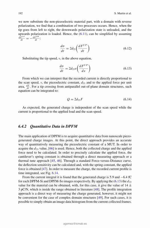
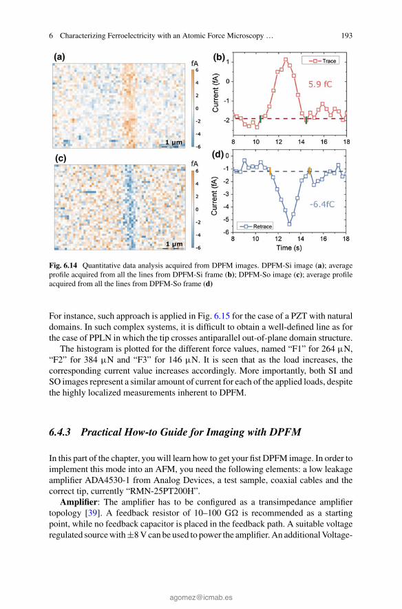
The main application of DPFM is to acquire quantitative data from nanoscale piezo-generated charge images. At this point, the direct approach provides an accurateway of quantitatively measuring the piezoelectric constant of a MUT. In order toacquire the d33 value, [66] is used. Hence, both the collected charge and the appliedforce need to be calculated. In order to precisely calculate the applied force, thecantilever’s spring constant is obtained through a direct measuring approach or athermal tune approach [45, 46]. Through a standard Force-versus-Distance curve,the deflection sensitivity can be calculated and, with the spring constant, the appliedforce is obtained [47]. In order to measure the charge, the recorded current profile istime integrated, see Fig. 6.14.
From the current integral it is found that the generated charge is 5.9 and −6.4 fCfor each DPFM-Si and DPFM-So images respectively. By applying the (6.13) the d33value for the material can be obtained, with, for this case, it give the value of 14 ±3 pC/N, which is inside the range obtained in literature [48]. The profile integrationapproach is a direct way of measuring the charge generated, however, it might notbe convenient for the case of complex domain structures [49]. For such cases, it ispossible to simply obtain an image data histogram from the current collected frames.
6 Characterizing Ferroelectricity with an Atomic Force Microscopy … 193
Fig. 6.14 Quantitative data analysis acquired from DPFM images. DPFM-Si image (a); averageprofile acquired from all the lines from DPFM-Si frame (b); DPFM-So image (c); average profileacquired from all the lines from DPFM-So frame (d)
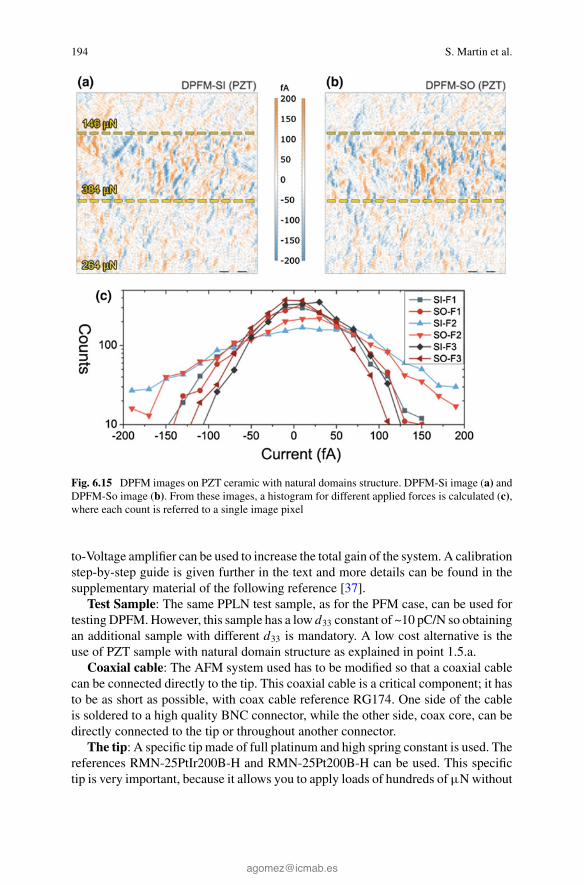
For instance, such approach is applied in Fig. 6.15 for the case of a PZT with naturaldomains. In such complex systems, it is difficult to obtain a well-defined line as forthe case of PPLN in which the tip crosses antiparallel out-of-plane domain structure.
The histogram is plotted for the different force values, named “F1” for 264 μN,“F2” for 384 μN and “F3” for 146 μN. It is seen that as the load increases, thecorresponding current value increases accordingly. More importantly, both SI andSO images represent a similar amount of current for each of the applied loads, despitethe highly localized measurements inherent to DPFM.
6.4.3 Practical How-to Guide for Imaging with DPFM
In this part of the chapter, you will learn how to get your fist DPFM image. In order toimplement this mode into an AFM, you need the following elements: a low leakageamplifier ADA4530-1 from Analog Devices, a test sample, coaxial cables and thecorrect tip, currently “RMN-25PT200H”.
Amplifier: The amplifier has to be configured as a transimpedance amplifiertopology [39]. A feedback resistor of 10–100 G� is recommended as a startingpoint, while no feedback capacitor is placed in the feedback path. A suitable voltageregulated sourcewith±8Vcan be used to power the amplifier.An additionalVoltage-
194 S. Martin et al.
Fig. 6.15 DPFM images on PZT ceramic with natural domains structure. DPFM-Si image (a) andDPFM-So image (b). From these images, a histogram for different applied forces is calculated (c),where each count is referred to a single image pixel
to-Voltage amplifier can be used to increase the total gain of the system. A calibrationstep-by-step guide is given further in the text and more details can be found in thesupplementary material of the following reference [37].
Test Sample: The same PPLN test sample, as for the PFM case, can be used fortestingDPFM.However, this sample has a low d33 constant of ~10 pC/N so obtainingan additional sample with different d33 is mandatory. A low cost alternative is theuse of PZT sample with natural domain structure as explained in point 1.5.a.
Coaxial cable: The AFM system used has to be modified so that a coaxial cablecan be connected directly to the tip. This coaxial cable is a critical component; it hasto be as short as possible, with coax cable reference RG174. One side of the cableis soldered to a high quality BNC connector, while the other side, coax core, can bedirectly connected to the tip or throughout another connector.
The tip: A specific tip made of full platinum and high spring constant is used. Thereferences RMN-25PtIr200B-H and RMN-25Pt200B-H can be used. This specifictip is very important, because it allows you to apply loads of hundreds ofμNwithout
6 Characterizing Ferroelectricity with an Atomic Force Microscopy … 195
permanently deformation the cantilever. More importantly, the tip is made of fullmetal, preserving the conductivity of a degraded tip.
Procedure: Once all these components are available the analysis can start andDPFM images collected. The tip is placed in the tip holder, and the laser is configuredas for the case of PFM. We recommend a feedback resistor of 10–100 G� forthe case of the transimpedance amplifier. The photodetector is adjusted with a lowlevel deflection signal-for instance, −3 V is a good starting point. With everythingconnected, the regulated voltage source can be connected to the low leakage currentamplifier. The output of the transimpedance amplifier can be routed to an additionalvoltage-to-voltage amplifier before feeding the signal into a suitable AUX inputchannel of your AFM controller If using such additional amplifier, check that thesignal read by the AFM is not saturated and correct to suitable REF input of thevoltage amplifier. The PPLN sample is connected to the ground, typical “samplebias”, through its bottom electrode. At this point, the tip can be approached towardsthe sample surface. For the first collected image, a set of recommended parametersare as follow: 128× 128 pixels, 25× 25 μm, speed of 0.1 ln/s and a deflection valueof 0 V. The signal recorded is the AUX input channel to which the transimpedanceamplifier output is connected, for both trace and retraces scan directions. This channelrelates to the current that is circulating through the transimpedance amplifier, andhence, it is the current that youwillmeasure. If topography channel looks like a PPLNsurface, then you can increase the load to the sample. Setpoint deflection value up to+3 V can be typically used without losing the topography PID signal path. If afterthis procedure, you are not able to record an image like the one shown in Fig. 6.12e,f you can do the following:
1. Use the AFM motor to apply to the sample a much higher load, as comparedto the force exerted by Z-piezo. The exact force value could reach the range ofmilliNewtons easily, making the tip blunt, and likely causing permanent damageto the cantilever. However, for testing purposes, you can do this in order to recorda signal similar than in the case of Fig. 6.12e, f. In order to do this step, ensurethat the piezo-scanner from the AFM is free to move, otherwise you may damageit. Use the AFMmotor to manually approach the tip to the PPLN sample surface,until the cantilever is considerably bended. The laser spot should go out of theprojection screen, but you could still enable the high voltage X and Y piezos andstart a 25 × 25 μm scan. Topography, Friction and Deflection frames should beconstant, but a suitable pattern similar to Fig. 6.12e, f would be recorded. Anexample of the frames recorded in this procedure is depicted in Fig. 6.16.This means that the setup is working correctly, but the leakage current is too high,and hence you have to find the leakage path and reduce it.
2. Increase the scan speed of the measurements to 1–2 ln/s. It is important, atthis step, to note that the tip remaining time for each image pixel has to belarger than the coefficient of 1/BW to ensure that the amplifier still behaves as atransimpedance amplifier and not as a charge amplifier.
3. Place an external resistor in the tip holder, so that the external resistor completesthe signal from the tip holder to ground. A suitable resistor, of 10–100 G�, can
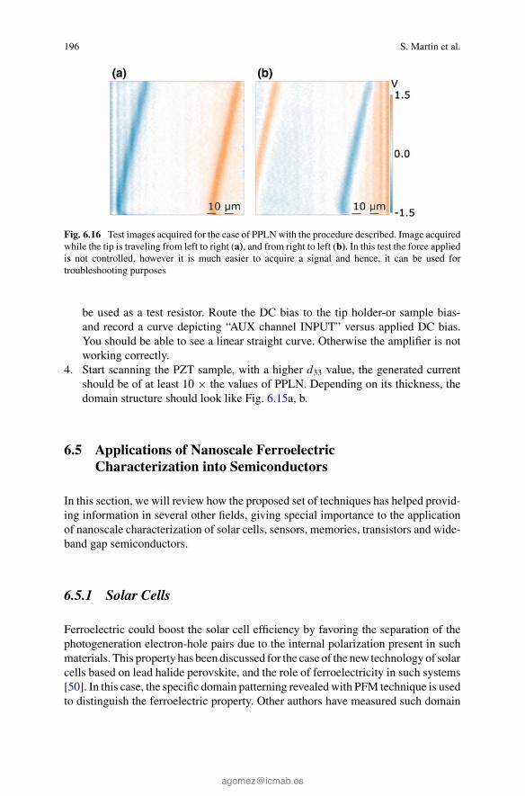
196 S. Martin et al.
Fig. 6.16 Test images acquired for the case of PPLNwith the procedure described. Image acquiredwhile the tip is traveling from left to right (a), and from right to left (b). In this test the force appliedis not controlled, however it is much easier to acquire a signal and hence, it can be used fortroubleshooting purposes
be used as a test resistor. Route the DC bias to the tip holder-or sample bias-and record a curve depicting “AUX channel INPUT” versus applied DC bias.You should be able to see a linear straight curve. Otherwise the amplifier is notworking correctly.
4. Start scanning the PZT sample, with a higher d33 value, the generated currentshould be of at least 10 × the values of PPLN. Depending on its thickness, thedomain structure should look like Fig. 6.15a, b.
6.5 Applications of Nanoscale FerroelectricCharacterization into Semiconductors
In this section, we will review how the proposed set of techniques has helped provid-ing information in several other fields, giving special importance to the applicationof nanoscale characterization of solar cells, sensors, memories, transistors and wide-band gap semiconductors.
6.5.1 Solar Cells
Ferroelectric could boost the solar cell efficiency by favoring the separation of thephotogeneration electron-hole pairs due to the internal polarization present in suchmaterials. This property has been discussed for the case of the new technology of solarcells based on lead halide perovskite, and the role of ferroelectricity in such systems[50]. In this case, the specific domain patterning revealed with PFM technique is usedto distinguish the ferroelectric property. Other authors have measured such domain
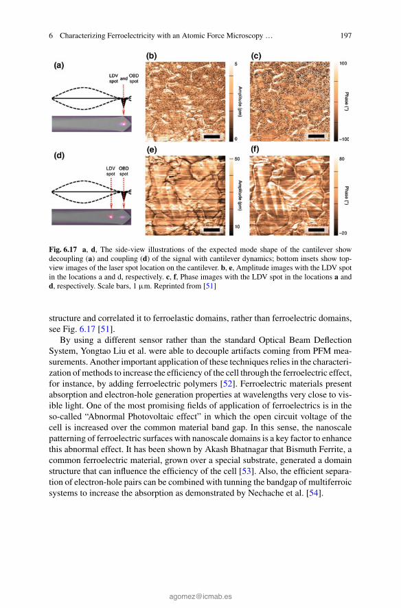
6 Characterizing Ferroelectricity with an Atomic Force Microscopy … 197
Fig. 6.17 a, d, The side-view illustrations of the expected mode shape of the cantilever showdecoupling (a) and coupling (d) of the signal with cantilever dynamics; bottom insets show top-view images of the laser spot location on the cantilever. b, e, Amplitude images with the LDV spotin the locations a and d, respectively. c, f, Phase images with the LDV spot in the locations a andd, respectively. Scale bars, 1 μm. Reprinted from [51]
structure and correlated it to ferroelastic domains, rather than ferroelectric domains,see Fig. 6.17 [51].
By using a different sensor rather than the standard Optical Beam DeflectionSystem, Yongtao Liu et al. were able to decouple artifacts coming from PFM mea-surements. Another important application of these techniques relies in the characteri-zation ofmethods to increase the efficiency of the cell through the ferroelectric effect,for instance, by adding ferroelectric polymers [52]. Ferroelectric materials presentabsorption and electron-hole generation properties at wavelengths very close to vis-ible light. One of the most promising fields of application of ferroelectrics is in theso-called “Abnormal Photovoltaic effect” in which the open circuit voltage of thecell is increased over the common material band gap. In this sense, the nanoscalepatterning of ferroelectric surfaces with nanoscale domains is a key factor to enhancethis abnormal effect. It has been shown by Akash Bhatnagar that Bismuth Ferrite, acommon ferroelectric material, grown over a special substrate, generated a domainstructure that can influence the efficiency of the cell [53]. Also, the efficient separa-tion of electron-hole pairs can be combined with tunning the bandgap of multiferroicsystems to increase the absorption as demonstrated by Nechache et al. [54].
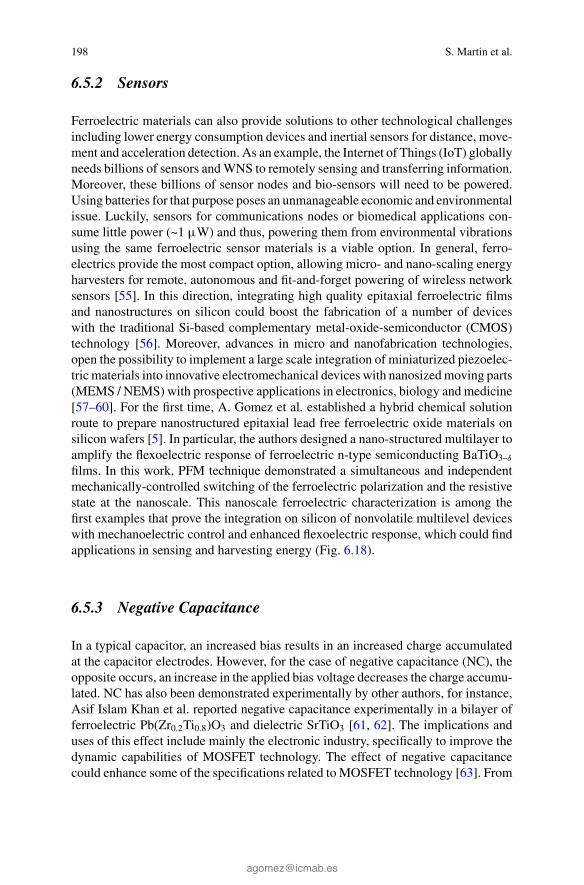
198 S. Martin et al.
6.5.2 Sensors
Ferroelectric materials can also provide solutions to other technological challengesincluding lower energy consumption devices and inertial sensors for distance, move-ment and acceleration detection. As an example, the Internet of Things (IoT) globallyneeds billions of sensors andWNS to remotely sensing and transferring information.Moreover, these billions of sensor nodes and bio-sensors will need to be powered.Using batteries for that purpose poses an unmanageable economic and environmentalissue. Luckily, sensors for communications nodes or biomedical applications con-sume little power (~1 μW) and thus, powering them from environmental vibrationsusing the same ferroelectric sensor materials is a viable option. In general, ferro-electrics provide the most compact option, allowing micro- and nano-scaling energyharvesters for remote, autonomous and fit-and-forget powering of wireless networksensors [55]. In this direction, integrating high quality epitaxial ferroelectric filmsand nanostructures on silicon could boost the fabrication of a number of deviceswith the traditional Si-based complementary metal-oxide-semiconductor (CMOS)technology [56]. Moreover, advances in micro and nanofabrication technologies,open the possibility to implement a large scale integration of miniaturized piezoelec-tric materials into innovative electromechanical devices with nanosizedmoving parts(MEMS / NEMS) with prospective applications in electronics, biology and medicine[57–60]. For the first time, A. Gomez et al. established a hybrid chemical solutionroute to prepare nanostructured epitaxial lead free ferroelectric oxide materials onsilicon wafers [5]. In particular, the authors designed a nano-structured multilayer toamplify the flexoelectric response of ferroelectric n-type semiconducting BaTiO3–δ
films. In this work, PFM technique demonstrated a simultaneous and independentmechanically-controlled switching of the ferroelectric polarization and the resistivestate at the nanoscale. This nanoscale ferroelectric characterization is among thefirst examples that prove the integration on silicon of nonvolatile multilevel deviceswith mechanoelectric control and enhanced flexoelectric response, which could findapplications in sensing and harvesting energy (Fig. 6.18).
6.5.3 Negative Capacitance
In a typical capacitor, an increased bias results in an increased charge accumulatedat the capacitor electrodes. However, for the case of negative capacitance (NC), theopposite occurs, an increase in the applied bias voltage decreases the charge accumu-lated. NC has also been demonstrated experimentally by other authors, for instance,Asif Islam Khan et al. reported negative capacitance experimentally in a bilayer offerroelectric Pb(Zr0.2Ti0.8)O3 and dielectric SrTiO3 [61, 62]. The implications anduses of this effect include mainly the electronic industry, specifically to improve thedynamic capabilities of MOSFET technology. The effect of negative capacitancecould enhance some of the specifications related to MOSFET technology [63]. From
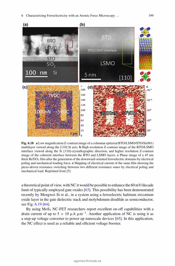
6 Characterizing Ferroelectricity with an Atomic Force Microscopy … 199
Fig. 6.18 a Lowmagnification Z-contrast image of a columnar epitaxial BTO/LSMO/STO/Si(001)multilayer viewed along the [110] Si axis. b High resolution Z-contrast image of the BTO/LSMOinterface viewed along the Si [110]-crystallographic direction, and higher resolution Z-contrastimage of the coherent interface between the BTO and LSMO layers. c Phase image of a 45 nmthick BaTiO3 film after the generation of the downward-oriented ferroelectric domains by electricalpoling and mechanical loading force. e Mapping of electrical current of the same film showing thepiezo-driven resistance switching between two different resistance states by electrical poling andmechanical load. Reprinted from [5]
a theoretical point of view,withNC itwould be possible to enhance the 60mV/decadelimit of typically employed gate oxides [63]. This possibility has been demonstratedrecently by Mengwei Si et al., in a system using a ferroelectric hafnium zirconiumoxide layer in the gate dielectric stack and molybdenum disulfide as semiconductor,see Fig. 6.19 [64].
By using MoS2 NC-FET researchers report excellent on-off capabilities with adrain current of up to 5 × 10 μA μm−1. Another application of NC is using it asa step-up voltage converter to power up nanoscale devices [65]. In this application,the NC effect is used as a reliable and efficient voltage booster.
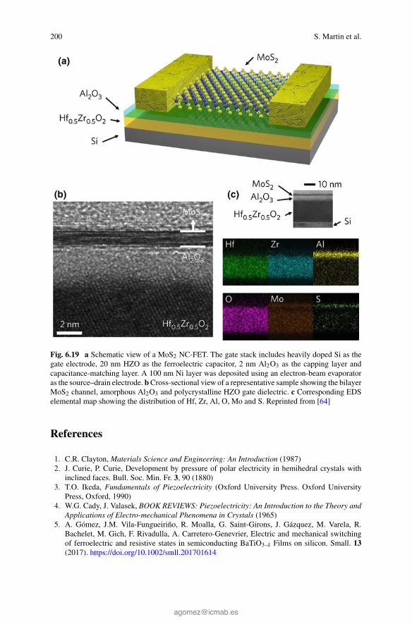
200 S. Martin et al.
Fig. 6.19 a Schematic view of a MoS2 NC-FET. The gate stack includes heavily doped Si as thegate electrode, 20 nm HZO as the ferroelectric capacitor, 2 nm Al2O3 as the capping layer andcapacitance-matching layer. A 100 nm Ni layer was deposited using an electron-beam evaporatoras the source–drain electrode. bCross-sectional view of a representative sample showing the bilayerMoS2 channel, amorphous Al2O3 and polycrystalline HZO gate dielectric. c Corresponding EDSelemental map showing the distribution of Hf, Zr, Al, O, Mo and S. Reprinted from [64]
References
1. C.R. Clayton, Materials Science and Engineering: An Introduction (1987)2. J. Curie, P. Curie, Development by pressure of polar electricity in hemihedral crystals with
inclined faces. Bull. Soc. Min. Fr. 3, 90 (1880)3. T.O. Ikeda, Fundamentals of Piezoelectricity (Oxford University Press. Oxford University
Press, Oxford, 1990)4. W.G. Cady, J. Valasek, BOOK REVIEWS: Piezoelectricity: An Introduction to the Theory and
Applications of Electro-mechanical Phenomena in Crystals (1965)5. A. Gómez, J.M. Vila-Fungueiriño, R. Moalla, G. Saint-Girons, J. Gázquez, M. Varela, R.
Bachelet, M. Gich, F. Rivadulla, A. Carretero-Genevrier, Electric and mechanical switchingof ferroelectric and resistive states in semiconducting BaTiO3–δ Films on silicon. Small. 13(2017). https://doi.org/10.1002/smll.201701614
6 Characterizing Ferroelectricity with an Atomic Force Microscopy … 201
6. H. Lu, C.W. Bark, D. Esque De Los Ojos, J. Alcala, C.B. Eom, G. Catalan, A. Gruverman,Mechanical writing of ferroelectric polarization. Science (80-.). 335, 59–61 (2012). https://doi.org/10.1126/science.1218693
7. H.D. Espinosa, R.A. Bernal, M.Minary-Jolandan, A review of mechanical and electromechan-ical properties of piezoelectric nanowires. Adv. Mater. 24, 4656–4675 (2012). https://doi.org/10.1002/adma.201104810
8. H. Lu, D.J. Kim, C.W. Bark, S. Ryu, C.B. Eom, E.Y. Tsymbal, A. Gruverman, Mechanically-induced resistive switching in ferroelectric tunnel junctions. Nano Lett. 12, 6289–6292 (2012).https://doi.org/10.1021/nl303396n
9. P. Sharma, S. Ryu, Z. Viskadourakis, T.R. Paudel, H. Lee, C. Panagopoulos, E.Y. Tsymbal,C.B. Eom, A. Gruverman, Electromechanics of Ferroelectric-Like Behavior of LaAlO3ThinFilms. Adv. Funct. Mater. 25, 6538–6544 (2015). https://doi.org/10.1002/adfm.201502483
10. R.K. Vasudevan, N. Balke, P. Maksymovych, S. Jesse, S.V. Kalinin, Ferroelectric or non-ferroelectric: why so many materials exhibit “ferroelectricity” on the nanoscale. Appl. Phys.Rev. 4 (2017). https://doi.org/10.1063/1.4979015
11. S.Xie,A.Gannepalli,Q.N.Chen,Y.Liu,Y.Zhou,R. Proksch, J. Li,High resolution quantitativepiezoresponse force microscopy of BiFeO3 nanofibers with dramatically enhanced sensitivity.Nanoscale 4, 408–413 (2012). https://doi.org/10.1039/C1NR11099C
12. S.V. Kalinin, E. Karapetian, M. Kachanov, Nanoelectromechanics of piezoresponse forcemicroscopy. Phys. Rev. B. 70, 184101 (2004). https://doi.org/10.1103/PhysRevB.70.184101
13. D. Seol, B. Kim, Y. Kim, Non-piezoelectric effects in piezoresponse force microscopy. Curr.Appl. Phys. 17, 661–674 (2017). https://doi.org/10.1016/j.cap.2016.12.012
14. E. Soergel, T. Jungk, A. Hoffmann, Quantitative analysis of ferroelectric domain imaging withpiezoresponse force microscopy. Cond-Mat/0510005. (2005)
15. S.Xie,A.Gannepalli,Q.N.Chen,Y.Liu,Y.Zhou,R. Proksch, J. Li,High resolution quantitativepiezoresponse force microscopy of BiFeO3 nanofibers with dramatically enhanced sensitivity.Nanoscale 4, 408 (2012). https://doi.org/10.1039/c1nr11099c
16. C. Harnagea, A. Pignolet, M. Alexe, D. Hesse, Piezoresponse scanning force microscopy: whatquantitative information can we really get out of piezoresponse measurements on ferroelectricthin films. Integr. Ferroelectr. 44, 113–124 (2002). https://doi.org/10.1080/10584580215148
17. J. Stephen, S. Jesse, J. Stephen, Quantitative mapping of switching behavior in piezoresponseforce microscopy. Rev. Sci. Instrum. 77, 73702 (2006)
18. A.S. Borowiak, N. Baboux, D. Albertini, B. Vilquin, G. Saint Girons, S. Pelloquin, B. Gau-tier, Electromechanical response of amorphous LaAlO3 thin film probed by scanning probemicroscopies. Appl. Phys. Lett. 105 (2014). https://doi.org/10.1063/1.4889853
19. A. Labuda, R. Proksch, Quantitative measurements of electromechanical response with a com-bined optical beam and interferometric atomic force microscope. Appl. Phys. Lett. 106 (2015).https://doi.org/10.1063/1.4922210
20. A. Gomez, T. Puig, X. Obradors, Diminish electrostatic in piezoresponse force microscopythrough longer or ultra-stiff tips. Appl. Surf. Sci. 439, 577–582 (2018). https://doi.org/10.1016/j.apsusc.2018.01.080
21. E.A. Eliseev, S.V. Kalinin, S. Jesse, S.L. Bravina, A.N. Morozovska, Electromechanical detec-tion in scanning probemicroscopy: tipmodels andmaterials contrast. J. Appl. Phys. 102 (2007).https://doi.org/10.1063/1.2749463
22. S.V. Kalinin, D.A. Bonnell, Imaging mechanism of piezoresponse force microscopy of ferro-electric surfaces. Phys. Rev. B—Condens. Matter Mater. Phys. 65, 1–11 (2002). https://doi.org/10.1103/physrevb.65.125408
23. N. Balke, P. Maksymovych, S. Jesse, A. Herklotz, A. Tselev, C.B. Eom, I.I. Kravchenko, P. Yu,S.V. Kalinin, Differentiating ferroelectric and nonferroelectric electromechanical effects withscanning probe microscopy. ACSNano 9, 6484–6492 (2015). https://doi.org/10.1021/acsnano.5b02227
24. G.A. MacDonald, F.W. DelRio, J.P. Killgore, Higher-eigenmode piezoresponse forcemicroscopy: a path towards increased sensitivity and the elimination of electrostatic artifacts.Nano Future 2, 015005 (2018). https://doi.org/10.1088/2399-1984/aab2bc
25. S.Martin, N. Baboux, D. Albertini, B. Gautier, A new technique based on current measurementfor nanoscale ferroelectricity assessment: nano-positive up negative down. Rev. Sci. Instrum.88 (2017). https://doi.org/10.1063/1.4974953
202 S. Martin et al.
26. S.V. Kalinin, D.A. Bonnell, Electric scanning probe imaging and modification of ferroelectricsurfaces. (2004), pp. 1–43. https://doi.org/10.1007/978-3-662-08901-9_1
27. S.V. Kalinin, S. Jesse, A. Tselev, A.P. Baddorf, N. Balke, The role of electrochemical phenom-ena in scanning probe microscopy of ferroelectric thin films. ACS Nano 5, 5683–5691 (2011).https://doi.org/10.1021/nn2013518
28. S. Martin, N. Baboux, D. Albertini, B. Gautier, Interpretation of multiscale characterizationtechniques to assess ferroelectricity: the case of GaFeO3. Ultramicroscopy 172, 47–51 (2017).https://doi.org/10.1016/j.ultramic.2016.10.012
29. H. Miao, C. Tan, X. Zhou, X. Wei, F. Li, More ferroelectrics discovered by switching spec-troscopy piezoresponse force microscopy? Epl. 108 (2014). https://doi.org/10.1209/0295-5075/108/27010
30. N. Balke, P. Maksymovych, S. Jesse, A. Herklotz, A. Tselev, C. Eom, I.I. Kravchenko, P. Yu,S.V. Kalinin, Differentiating ferroelectric and effects with scanning probe microscopy. ACSNano 9, 6484–6492 (2015). https://doi.org/10.1021/acsnano.5b02227
31. J.F. Scott, L. Kammerdiner, M. Parris, S. Traynor, V. Ottenbacher, A. Shawabkeh, W.F. Oliver,F. Scott, Switching kinetics of lead zirconate titanate submicron thin-film memories. 64, 787(2007). https://doi.org/10.1063/1.341925
32. I. Estevez, P. Chrétien,O. Schneegans, F.Houzé, Specificmethodology for capacitance imagingby atomic force microscopy: a breakthrough towards an elimination of parasitic effects. Appl.Phys. Lett. 104 (2014). https://doi.org/10.1063/1.4866607
33. S. Tiedke, T. Schmitz, K. Prume, A. Roelofs, T. Schneller, U. Kall, R. Waser, C.S. Ganpule,V. Nagarajan, A. Stanishevsky, R. Ramesh, Direct hysteresis measurements of single nano-sized ferroelectric capacitors contacted with an atomic force microscope. Appl. Phys. Lett. 79,3678–3680 (2001). https://doi.org/10.1063/1.1421638
34. K. Prume, A. Roelofs, T. Schmitz, B. Reichenberg, S. Tiedke, R. Waser, Compensation ofthe parasitic capacitance of a scanning force microscope cantilever used for measurements onferroelectric capacitors of submicron size by means of finite element simulations. Japan. J.Appl. Phys., Part 1 Regul. Pap. Short Notes Rev. Pap. 41, 7198–7201 (2002). https://doi.org/10.1143/jjap.41.7198
35. T. Schmitz, K. Prume, B. Reichenberg, A. Roelofs, R. Waser, S. Tiedke, In-situ compensationof the parasitic capacitance for nanoscale hysteresis measurements. J. Eur. Ceram. Soc. 24,1145–1147 (2004). https://doi.org/10.1016/S0955-2219(03)00583-1
36. A.V. Ievlev, A.N. Morozovska, V.Y. Shur, S.V. Kalinin, Humidity effects on tip-induced polar-ization switching in lithium niobate. Appl. Phys. Lett. 104 (2014). https://doi.org/10.1063/1.4867979
37. A. Gomez, M. Gich, A. Carretero-Genevrier, T. Puig, X. Obradors, Piezo-generated chargemapping revealed through direct piezoelectric force microscopy. Nat. Commun. 8 (2017).https://doi.org/10.1038/s41467-017-01361-2
38. K. Uchino, Piezoelectric Actuators and Ultrasonic Motors (Springer Science & BusinessMedia, 1997)
39. P.R. Gray, R.G. Meyer, Analysis and Design of Analog Integrated Circuits (1984)40. I. Hickman, Analog Electronics (1999)41. J.R. Singer, Operational amplifiers, theory and practice. Proc. IEEE 64, 1456 (1976). https://
doi.org/10.1109/PROC.1976.1035842. F. Tavernier, M. Steyaert, High-Speed Optical Receivers with Integrated Photodiode in
Nanoscale CMOS (2011)43. P.T. Krein, Elements of Electronics (1998)44. P.E. West, Atomic Force Microscopy (2007)45. J.L. Hutter, J. Bechhoefer, Calibration of atomic-force microscope tips. Rev. Sci. Instrum. 64,
1868–1873 (1993). https://doi.org/10.1063/1.114397046. N.A. Burnham, X. Chen, C.S. Hodges, G.A. Matei, E.J. Thoreson, C.J. Roberts, M.C. Davies,
S.J.B. Tendler, Comparison of calibration methods for atomic-force microscopy cantilevers.Nanotechnology 14, 1–6 (2003). https://doi.org/10.1088/0957-4484/14/1/301
47. H.J. Butt, B. Cappella, M. Kappl, Force measurements with the atomic force microscope:Technique, interpretation and applications. Surf. Sci. Rep. 59, 1–152 (2005). https://doi.org/10.1016/j.surfrep.2005.08.003
6 Characterizing Ferroelectricity with an Atomic Force Microscopy … 203
48. R.S.Weis, T.K.Gaylord, Lithiumniobate: Summaryof physical properties and crystal structure.Appl. Phys. A Solids Surf. 37, 191–203 (1985). https://doi.org/10.1007/BF00614817
49. A. Gruverman, O. Auciello, H. Tokumoto, Scanning force microscopy for the study of domainstructure in ferroelectric thin films. J. Vac. Sci. Technol., B 14, 602–605 (1996)
50. H. Röhm, T. Leonhard, M.J. Hoffmann, A. Colsmann, Ferroelectric domains in methylammo-nium lead iodide perovskite thin-films. Energy Environ. Sci. 10, 950–955 (2017). https://doi.org/10.1039/C7EE00420F
51. Y. Liu, L. Collins, R. Proksch, S. Kim, B.R. Watson, B. Doughty, T.R. Calhoun, M. Ahmadi,A.V. Ievlev, S. Jesse, S.T.Retterer,A.Belianinov,K.Xiao, J.Huang,B.G.Sumpter, S.V.Kalinin,B. Hu, O.S. Ovchinnikova, Chemical nature of ferroelastic twin domains in CH3NH3PbI3perovskite. Nat. Mater. 1 (2018). https://doi.org/10.1038/s41563-018-0152-z
52. Y. Yuan, T. Reece, P. Sharma, Efficiency enhancement in organic solar cells with ferroelectricpolymers. Nat. Mater. 10, 296–302 (2011). https://doi.org/10.1038/nmat2951
53. A. Bhatnagar, A. Roy Chaudhuri, Y. Heon Kim, D. Hesse, M. Alexe, Role of domain walls inthe abnormal photovoltaic effect in BiFeO3. Nat. Commun. 4 (2013). https://doi.org/10.1038/ncomms3835
54. R. Nechache, C. Harnagea, S. Li, L. Cardenas, W. Huang, J. Chakrabartty, F. Rosei, Bandgaptuning of multiferroic oxide solar cells. Nat. Photonics 9, 61–67 (2014). https://doi.org/10.1038/nphoton.2014.255
55. Kompis, C.: Energy harvesting technologies to enable remote and wireless sensing. Security.20, 2010 (2008)
56. R. Guo, Z. Wang, S. Zeng, K. Han, L. Huang, D.G. Schlom, T. Venkatesan, Ariando, J. Chen,Functional ferroelectric tunnel junctions on silicon. Sci. Rep. 5 (2015). https://doi.org/10.1038/srep12576
57. M.P. Warusawithana, C. Cen, C.R. Sleasman, J.C. Woicik, Y. Li, L.F. Kourkoutis, J.A. Klug,H. Li, P. Ryan, L.-P. Wang, M. Bedzyk, D.A. Muller, L.-Q. Chen, J. Levy, D.G. Schlom, Aferroelectric oxide made directly on silicon. Science (80-.). 324, 367–370 (2009). https://doi.org/10.1126/science.1169678
58. R. Ramesh, MATERIALS SCIENCE: Orienting ferroelectric films. Science. 296, 1975–1976(2002). https://doi.org/10.1126/science.1072855
59. S.H. Baek, J. Park, D.M. Kim, V.A. Aksyuk, R.R. Das, S.D. Bu, D.A. Felker, J. Lettieri,V. Vaithyanathan, S.S.N. Bharadwaja, N. Bassiri-Gharb, Y.B. Chen, H.P. Sun, C.M. Folkman,H.W. Jang, D.J. Kreft, S.K. Streiffer, R. Ramesh, X.Q. Pan, S. Trolier-McKinstry, D.G. Schlom,M.S. Rzchowski, R.H. Blick, C.B. Eom, Giant piezoelectricity on Si for hyperactive MEMS.Science (80-.). 334, 958–961 (2011). https://doi.org/10.1126/science.1207186
60. H.G. Craighead, Nanoelectromechanical systems. Science (80-.). 290, 1532–1535 (2000).https://doi.org/10.1126/science.290.5496.1532
61. A. IslamKhan,D.Bhowmik, P.Yu,S. JooKim,X.Pan,R.Ramesh, S. Salahuddin,Experimentalevidence of ferroelectric negative capacitance in nanoscale heterostructures. Appl. Phys. Lett.99 (2011). https://doi.org/10.1063/1.3634072
62. A.I. Khan, K. Chatterjee, B. Wang, S. Drapcho, L. You, C. Serrao, S.R. Bakaul, R. Ramesh, S.Salahuddin, Negative capacitance in a ferroelectric capacitor. Nat. Mater. 14, 182–186 (2015).https://doi.org/10.1038/nmat4148
63. A.I. Khan, C.W. Yeung, C. Hu, S. Salahuddin, Ferroelectric negative capacitance MOSFET:capacitance tuning&antiferroelectric operation. Tech.Dig. Int. Electron.DevicesMeet. IEDM.(2011). https://doi.org/10.1109/iedm.2011.6131532
64. M. Si, C.-J. Su, C. Jiang, N.J. Conrad, H. Zhou, K.D. Maize, G. Qiu, C.-T. Wu, A. Shakouri,M.A. Alam, P.D. Ye, Steep-slope hysteresis-free negative capacitance MoS2 transistors. Nat.Nanotechnol. 13(1) (2017). https://doi.org/10.1038/s41565-017-0010-1
65. S. Salahuddin, S. Datta, Use of negative capacitance to provide voltage amplification for lowpower nanoscale devices. Nano Lett. 8, 405–410 (2008). https://doi.org/10.1021/nl071804g
66. A. Gomez, M. Gich, A. Carretero-Genevrier, T. Puig, X. Obradors, Piezo-generated chargemapping revealed through direct piezoelectric force microscopy. Nat. commun. 8(1), 1113(2017)