Embed Size (px)
Citation preview

UNCLASSI FIED
294.655AD_
M~1e
ARMED SERVICES TECHNICAL INFORMATION AGENCYARLINGTON HALL STATIONARLINGTON 12, VIRGINIA
"'- I LI7,.E I
UNCLASSIFIEDREPRODUCED FROM
BEST AVAILABLE COPY

NOTICE: When government or other drawings, speci-fications or other data are used for any purposeother than in connection with a definitely relatedgovernment procurement operation, the U. S.Government thereby incurs no responsibility, nor anyobligation whatsoever; and the fact that the Govern-ment may have formulated, furnished, or in any waysupplied the sanid drawings, specifications, or otherdata is not to be regarded by implication or other-wise as in any manner licensing the holder or anyother person or corporation, or conveying any rightsor permission to manufacture, use or sell anypatented invention that may in any way be relatedthereto.

FIFTH QUARTERLY REPORT
COMPATIBLE TECHNIQUES
FORINTEGRATED CIRCUITRY
C" U. S. AIR FORCE
CONTRACT NO. AF33(616)8276
C:) L./...J •;.• ~ ~~~~~Period Covered ,..... _'' •--
prepared for
U.S. AIR FORCE
AERONAUTICAL SYSTEMS DIVISIefr"
WRIGHT-PATTERSON AIR FORCE BASE, OHIO
MOTOROLA Semiconductor Product.s Ina.15005 EAST M COOW) LL. FVOAD PHOENIX, ARIZONA A ,-(L1IltH.AIN'l (•f MOTORO( A INCI

FIFTH QUARTERLY REPORT
COMPATIBLE TECHNIQUES FOR INTEGRATED CIRCUITRY
PERIOD OF
i MAY 1962 to 31 JULY 1962
UNITED STATES AIR FORCE
1 CONTRACT NO. AF 33(616)-8276
1
Prepared for........
UNITED STATES AIR FORCF
AERONAUTICAL SYSTEMS DIVISION
WRIGHT-PATTERSON AIR FORCE BASE, OHIO
Prepared by . . .
MOTOROLA, INC,
SEMICONDUCTOR PRODUCTS DIVISION
PHOENIX, ARIZONA
I
I

INDEX
Section Title Pa•
1.0 Introduction . . ,. . . . . . . . .... . 1
2 0 Basic Material Studies .... ... 22.1 Open Tube Epitaxial GaAs .... .. 22.2 Incremental Sheet Resistivity in Doped
P-type Films ............. 62.2.1 Material . . . . . . . . . . . 62.2.2 Procedure ......... ...... .. . . 62.2.3 Results 7........... ..... 72.2.4 Discussion 10.......... 102.3 Sheet Resistivity Gradients Through
Epitaxial Films 1............ .1i
2. . Material . . . . . . . .. i
2.3.2 PLocedure ................. 112.3.3 Results and Discussion .......... .. 123.0 Thin Film Technology ... ........ .... 163.1 Vapor Deposition of Glass Films . 163,2 Tantalum Oxide Capacitors ....... .... 193.3 Thin Film Inductors for Transceivers . 203,4 Silicon Monoxide C~pacitors ......... 233.5 Tin OxideResistors ....... 243.6 Interconnection of Integrated Circuit
Submodules ... .. ............ .. 29
4 0 Silicon Process and Integrated CircuitTechnology ..................... 37
4 1 Epitaxial Diffused Integrated Circuits . 374.1.1 Optimized Structure for Integrated
Circuits .............. . 37
-i.
I

Section Title Page
4.1.2 PNP Integrated Circuits ...... . . . 46
4.2 Bonding Reliability Studies . . . . . . . 51
4.3 Diffused Resistor TemperatureCoefficients ................. 53
4.4 Metallization . .. .. .. .. ...... ....... 534.4.1 Contact Studies ....... ....... . 604.4.2 Summary .......... ... . . 65
4.5 Testing of Monolithic Integrated Circuits 654.6 Optimized Structure for Integrated
Circuits . . . . . . . . . . . . .. . . 724.6.1 High Frequency Integrated Amplifier . . . 72
4.6.2 MECL Circuits .... ......... .. . . . 734.6.3 Transistor Structures in Integrated
Circuits . . . . . . . . . . . . . . . . 73
4.7 "Rust"Problem . . ........ . .. 76
4.8 Process Control .... ............. ... 794.8.1 Test Patterns .............. ...... 79
4.9 Resistor Evaluation in IntegratedCircuits . . . . . . . . . . . .. .. . . 81
5.0 Advanced Circuit Design Studies .... 93
5.1 DCTL (Direct Coupled Transistor Logic). . 935.1.1 DCTL Current Hogging Analysis ... . 955.2 MECL . . ......... . . . . . . 975.3 DTL . . . . .# . . . . . . . . . . . . 98
6.0 UHF Transceiver Design and Fabrication, . 1136.1 Fabrication of Hybrid IntegratedCircuits . . . . . . . . . . . . . . .. 113
-ii -
I.

Section Title Page
6.2 Crystal Filters ...... . . . . . . . . 116
6.3 Inductor Development and Other NewHybrid Circuit Elements. . . . . . . .. 116
6.4 Interim Model Transceiver . ....... . 120
6.5 Hybrid Integrated Linear Amplifier. . .. 121
6.6 Status of Hybrid Integrated TransreceiverCircuits . . . . . . . . . . . . . . . . 126
6.7 H.I.C. Fabrication Techniques . . . . .. 131
6.8 Transreceiver Model Construction . .... 133
6.9 FEB Linear Amplifiers . . . . . 135
7.0 PCM Telemetry System . . . .... 147
7.1 Multiplexer Switching . . . .... 147
7.2 Comparator Amplifier . . ...... . 148
7.3 Isolation Amplifier . . . .. . 149
7.4 Encoder/Decoder ..... ....... . .. 149
- iii -
I,

1
loO INTRODUCTION
This report covers the fifth quarter's efforts in
developing CompaLible Techniques for Integrated Circuitry on
contract AF 33(616)-8276.
Most of the effort to date has been spent in developing
process techniques which are necessary for Integrated Circuit
fabrication.. This effort has been both in morphological areaR
and thin films as applied to semiconducting substrate.
Further efforts in perfecting our epitaxial techniques
are reported. A program has been started to develop and fabricate
typical circuits which are practical for a wide range of high and
low frequency amplifier appllcaLlons as well as logic circuits.
I.
-1

2.0 BASIC MATERIAL STUDIES
2.1 Open Tube Epitaxial GaAs
The gas flow system was redesigned to obtain bettercontrol. The present system is shown in Figure 1.
1 '1I> Furnace
flow !flow coldmeters Imeter trap
H2 HCl
vent
FIGURE 1
Several intermittent leaks were detected and closed.The HCl supply was replaced and the H2 purity checked to eliminateas much contaminaLion as possible, Oxygen content of the H2 after
purification reads 1.3 ppm.
"-2 -
I

The quartz boats are being etched in the furnace between
runs. Hydrogen and HC1 are mixed and added as an etchant over the
deposition area of the boat which is held at about 1050*C.
P-type (111) wafers are being used as substrates. This
will allow capacitance measurements of the film to be made and
allow easier thickness determinations.
N-type films have been deposited on P-type GaAs sub-
strates for evaluation purposes. The interface appears flat and
without apparent diffusion. The etchant used for developing the
interface consists of 1.0 ml of 5% naOH and one drop of H2 02 . See
Figure 2. Mesas were etched on several samples and breakdowns
measured at 8 - 10 volts without attempts at controlling surface
condiLions. Carrier con•enLtraLivni of Lhu P-Lype substrate was
approximately 107/cm3 . Capacitance measurements made on these
fiLms indicate the film carrier concentration to be somewhat1.7 3higher than 10 /cm . More definite data can be obtained on
higher doped subhtrates.
Deposition has been occurring during the preheat cycle
without the presence of a minimum amount of HCI. The gas system
was further modified to insure no release of hung-up HCI during
the hydrogen purge and preheat. Analysis of the gas stream
through AgNO 3 indicates no HCl present, The possibility remains
thai a small amount; of oxygen in the gas stream could be trans-
porting gallium and leading to deposition of GaAs on the substrAtes.
This deposition is epitaxial and although quite thin, is
uncontrolled. If the transporting agent cannot be found and
eliminated, deposition on the wafers can be reduced by changes
in the gas flows during the preheat.
-3 -
Ii
I
.1 .
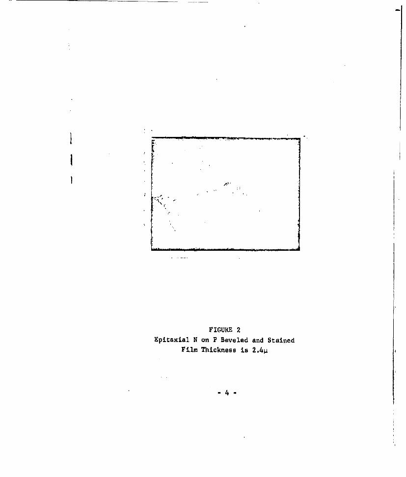
FIGURE 2Epitaxial. N on P Beveled and Stained
Film Thickness is 2.4p
"4-

I
Deposition occurring during the preheat cycle under aH2 atmosphere was studied during this period. As previously
reported, the film is epitaxial, but uncontrolled. Current testsindicate a one-hdur preheat is necessary to bring boat, sourceand substrates to temperature before introducing growth flow rates.
Although a palladium silver alloy diffusion unit wasused as the source of pure hydrogen, hygrometer readings indicate
some moisture presenr. A small amount could possibly be trans-porting gallium and causing pre-deposition on the substrates.Extensive measures have been taken to reduce the moisture content
by utilizing molecular sieve drying towers and dry ice and acetone
cold traps, but the problem remains, The dry ice and acetone
traps proved unsatisfactory since any moisture trapped reacted
with the hydrogen chloride gas forming hydrochloric acid. A
certain amount of hydrogen chloride gas passed through the cold
trap and the growth reaction was carried out. Since the growth
rate is very dependent on the percentage of HCl in the gas stream,small variations in the IICI content caused by the reaction in the
cold trap made control of the growth rate difficult,
To side-step this problem, a gas phase etching processproved effective. During the preheat cycle an excess of HCI is
introduced and the I2 increased from 300 c/mrin. to 1000 cc/min.,therefore, decreasing the efficiency of the HCI over the source.The UCl does not reach equilibrium over the source and continues
L• etch the substrates. At a mixture ratio of 800:1 (H2 HCI)with a total flow stream of 1000 co/mmin; smooth, planar etchedsurfaces were obtained on the GaAs -':11> B face.
"-5-

Growth conditions are established subsequent to the
etch cycle by decreasing the total concentration of H2 + HCI to
300 cc/min. at a ratio of 1000:1 (H2 :HCl). Film surfaces appearas an inverted "orange peel" effect. This can be rectified by
varying flow rateq and amount of source.
Initial experiments have not produced comparable
resiilts on the GaAs <111> A face. A one-zone resistive furnaceand apparatus is being assembled for further development of gas
phase etching.
2.2 Incremental Sheet Resistivity in Doped P-type Films
2.2.1 Material
Two epitaxial wafers, 1012-9 and 1012-7 were used in
these anodizations. The N-type substrate of both had a bulk
resistivity of 0.01 (i cm to 0.02 !! cm. The P-type epi-film of
1012-9 has a bulk resistivity of 0.096 U cm and an estimated
(from the growth curve) depth of 3 ýt. The N-type substrate wasarsenic doped and gas etched before the bo:ron (loped epi-film was
grown automatically.
2.2.2 Procedure
A piece from the edge of 101.2-9 was removed, beveledand stained to check the P-layer thickness. The depth varied
from 1.77 it to 2.07 P for an average of 2.01 ý1. A mesa area of
0.635 cm2 was etched on each wafer by immersion in CP-4 for 30
seconds.
-6

The anodization apparatus was set up l) and 10 minute
runs were carried out on each wafer. After each run, the oxide
was removed with HF° After every thicd run, the sheet resistiv-
ities were measured and after every ninth run, the wafers were
weighed. Both wafers probed N-type after 39 runs. The amount
of silicon removed was calculated for each wafer using the weight
loss, density of silicon and mesa area. The average resistivities,
PL (ohm-cm), in the removed layers, At(cm), were calculated using
the formula:
- 4.4E2 E1 AtT E -E IP 2L 212
were E2 is the voltage drop (volts) across the four-point probepoints before removal of At; E 1 is the voltage drop across the
points after removal of At; 12 is the current flow after removal
of At.
2.2.3 Results
The results of the two experiments are summarized inTable I.
The total amount of silicon removed from each wafer
was 3.64 4, slightly more than that originally predicted, 3 4.
The average amount determined by staining a piece of 1012-9, 2.01 .,
was much less that the amount removed, This large discrepancy may
be due to a falling off in upitaxial growth near the edges of the
(1)j. E. McNamara and II. M, Robertson, "METHODS FOR MEASURING
RESISTIVITY GRADIENTS AND THICKNESSIES IN EPITAXIAL F[LMS,"
Technical Note #9, Material Diffusion Laboratory.
-7-

TABLE I
1012-9 1012-7
Run tAt By Weight OL I By Weight; 0.81 0o1867 ncm
3 0.28 k 0.2546 ncmI 0.28 c
6 0.28 0.1167 0.28 0.09339 0.28 0.1000 0.28 0.0824
12 0.28 0.1037 0.28 0.0933
15 0.28 0.1273 0.28 0.100018 0.28 0.1037 0.28 0.0903
21 0 28 0.1037 0.28 0.0903 1
24 ' 0,28 0.1037 0.28 0.0903
27 0.28 0.1167 0.28 0.1037
30 0.28 0.28 0.1000
33 0.28 - 0.28 0.1167
36 0.28 - 0.28 -
39 0.28 - 0.28 -
wafer. Previous to these anodizations, a piece near the edge ofwafer 1012-8 was beveled and stained and found to have a P-layer
depth of 3.52 . average.
A comparison of the resistivities obtained by using
At from the color method (published values for oxide thicknessas a function of interference color) and At derived from the
staining method are summarized in Table 2.
-8

a
N 41 b. . 1
I ~ 0 00 ý 1cý a 00.0 00 0
0~ 0 00 0 00 0
0 0 H. '0 c.0 '.0 '0 '0 N0 '0 0 '.0A .N 0 H rlý0rHHHD%0 L NHH% y
0 0 0 8c ~ ;8 ýc
H C~r )e n m m e ne
0 c4C H 0 0(iC I S~ m
In % fl% 0" N SOt N
0- 0 00r%00Ln00%D0II I
0 CIO 000 000 00
0n0a .D jr%% 5 uu'0. 0 0 0
NG 00 000000L
r4 4 H H "4 ,4 ,4 H rq H H ,.
o;C 8C 0 o U C aI I (H nlm
(nOUN 0(
-9

2.2.4 Discussion
Sheet resistivity readings were taken with a 25-mii
germanium probe. The points on this probe are rounded in com-
parison to the points of 25'miU and 50-mij1 silicon probes used
in previous experiments. It appears that the rounded points
permit readings to be taken after a larger number of anodizations
than the sharper points. The surfaces measured with the sharp
points are scratched and marred suggesting that the points
penetrate through the P-layer.
Bulk resistivities calculated from sheet resistivity
readings taken before anodization-and the total depth are higher
than those reported in both cases, 0.1184 vs. 0.096 flcm for 1012-9
and 0.1027 vs. 0.084 Orm for 1012-7. The reslsttvities after the
first three anodizations show a sharp decrease. The resistivities
drop and then reach another peak about one-third of the distance
through the layer before leveling off. As the junction isapproached, the curve slopes upwaid. The similarity between the
two curves is striking. Even the points lying off the curves areapproximately the same distance away from their respective curves.
Both the color and the staining methods prevent problems
which cannot be ignored. ft was observed previously (2) that the
weight change method indicates a 20%. less thick silicon removal
than would be calculated from published values for oxide thickness
as a function of interference col.or. These experiments show a
15% less thick silicon removal. The staining method is probably
not accurate when measurements are taken as close to the edge of
the wafer as they are in this case.
(2) Op. Cit.
S10

2.3 Sheet Resistivity Gradients Throuph Epitaxial Films
2.3.1 Material-L
Six silicon wafers were anodized since the last reportand resistivities were measured after every third anodization.Wafer 525-2 (P-n-N structure; P-layer 0.0587 ocm; N+ -substrate0.0032-0.0015 Qcm) was anodized 28 times before the N-layer wasreached. Wafers 505-1 (P-N-N+ structure; P-layer 0.0372 Qcm;
-N+ substrate 0.015-0.025 ncm) and 505-2 (P-N~N+ structure;P-layer 0,0585 0cm; N+ - substrate 0.015 025 0cm) were anodized
28 and 10 times respectively. Wafers Z-14-6, Z-14-7 and Z-14-8
(P-N structure; P-layer 0.00745 0cm; N-substrate 0.1 0cm) were
anodized 15, 44 and 23 times respectively.
2,3.2 Procedure
Various oxide thicknesses were grown on each wafer byincreasing the current density and/or increasing the anodizationtime in order to siced up the entire process., Wafers Z-14-6, 7and 8 were also anodized with the apparatus(3') slightly modifiedso that two wafers coutld be anodiL t the same time. The modi-fications con;isted of two holes i, g cut Into the polyethylenebeaker and two rubber seals being used. A t-shaped piece of glasstubing was inserted into the surgical tubing and two polyethylenetubes were attached to this by more surgical tubing, Thus, thecirculating pump sent the electrolyte through the T'-tube and onto
(3).% E. McNamara and H. M. Robertson, "METHODS VOR MEASURINGRESISTIVITY GRADIENTS AND THICKNESSES YN EPUIAX.AL FILMS,"Technical Note #9, Materials Diffusion Laboratory
- 1].-

I the surface of two wafers at the same time, These modifications
decreased the time element by a small amount and allowed the
1, resisLivities to be compared as the experiment progressed,
1 2.3.3 Results and Discussion
I Sheet resistivity measurements all showed a dip in thecurve for the first 9 to 12 anodizations as shown in Figures 3and 4, and Table 3,. The resistivities appear to be high near the
!I surface of the wafer, decrease after a few increments have beenremoved, and rise again after a few more are removed. This samecurve was also shown for wafers 1012-7 and 1012-9 in the reportfor May 1962.t
There is a striking similarity between the curves ofwafers Z-14-6 and 7 which are from the same furnace run. Workwill be continued on wafers from a single furnace run to see ifthey show curves similar to each other.
- 12 -

177~~ ~~ IGI.. .. ..
TT 1 i A_
AT - fI~74I~ ~~Th-- T_474 :4=4
ZZF
F =tHL 7 7 2
Z_, 417ýJ . j__"
-tIt
-I:7
EliZ J_;
IL 4E4-iŽix.J jj + I

w- -7
F J., J j. 4:4 4-tZ 7- H
____w
I M__ -1
L.Z.Z. _
_tt I' Z
LI I
FFt-
+I I - it .
L_ J .II~~iJ Lj*
7.0 -

-- -- -
~~-1N (XI H H -I c'.)
co 00 0 0 C
1*o
N~~M CYN i
( ~ 0 0 C) 0 0 ; L3 C
V\r4 C C-. C-o N- L--
CXI (Xi IXI cX (Y\ I I
I~0.
'.0 C'-
(D ci CM cm I(1 C) ,;
C) a'-I-No o.
.- ji) (f C?) W ~ I l N I I I
("' C '. 0r' X \ ' ' X
H ( 0 0 CC) C') r) ) 0 )
oo 0
i~*d C)9 C) Ci
N0 0 0 0 0; C-) Q- 0
Co 0 ' C
CXm \~0 0 G\ CV 0 0
rRH r, CXI- m

._1-0 THIN FILM TECHNOLOGY
3.1 Vapor Deposition of Glass Films
The purpose of this task is to develop means fordepositing glass films onto semiconductor substrates, utilizingthe technologies which are compatible with sem'conductingmaterials and with other thin films. The films are under inves-tigation for use as: (a) dielectric films for capacitors, and
(b) electrical insulating films for conductor crossover insulation,
A series of investigations were conducted to determinethe optimum parameters for deposition of various types of films
during this reporting period. Significant results from theseinvestigations iuclude the following: Preliminary resultsindicate that A12 03 Sio2 capacitors can be manufactured totolerances of ±10% in capacitance value.
During this reporting period a group of 15 A1 2 03 'Sio 2capacitors were fabricated for environmental test purposes, Afterapproximately 400 hours at 125'C with 12 volts DC electrical stressapplied, one unit out of fifteen showed electrical short circuiting.Two other units, however, showed evidence of having shorted during
the test, with subsequent healing of the shorts by the "burningoff" of the top electrode over the shorted area. These healedshorts are reflected by a large decrease in capacitance (30 to 50r.)
for these units, The remaining capacitors showed an averagedecrease of about 6% in capacitance., No significant change inleakage current or dissipation factor was noted for the remaining
12 capacitors.
" 16
During the previous reporting period, a number of
A' 2 03 oSi0 2 capacitors were fabricated at a range of different
dielectric deposition temperatures to study the effect on capacitorproperties of the temperature of deposition of the dielectric,
Evaluation of these capacitors has shown that the dielectricconstant of the films is essentially independent of the depositiontemperature, the dissipation factor of the films decreases by asmall amount as the deposition temperature rises, and the DC
leakage current of the capacitors is a comparatively strong
function of deposition temperature.
These capacitors will later be put on environmental
tests to determine any relationships that may exist between thecapacitor life expectation and the dielectric deposition temperature.Figure I shows the behavior of capacitance vs. temperature for a
capacitor. The temperature coefficient of the capacitor variesfrom 135 ppm measured at 100 kilocycles per second to 420 ppm when
measured at 100 cycles per second
Life tests on the aluminosilicate capacitors initiated
during the preious reporting period were continued this period
until a malfunction'of the test chamber caused the tests to beterminated after 720 hours of test time.. These capacitors were
fabricated on five substrates, each substrate containing three
capacitors, All six of the capacitors on two of the five substrates
failed within the first 50 hours of the test. No failures weredetnr.ted, however, un the remaining nine capacitors on the other
three substrates during the entire test period. It is interesting
to note that, discounting the six early failures, that theremaining capacitors accumulated over 6500 unit hours of testingat 12 volts DC potential in an environment of 125*C with no failures.
- 17 -
At

Hiti i ;wt'HI~~ ~ +3 U-h i- I. i
ro 1.*- t i01
....... ... . ..
-~~~ X '!
*Il ii w'I 'i j , 4 I I 4 I; ; I
* 4 ~ 1 1 4
l it :~I,
-r8 -7 . ....
18 Fizure I

The nine capacitors surviving the life tests exhibited an average-...decrease in capacitance of 31% over the pr'ýriod of testing,. No
significant change in dissipation factor or DC leakage resistanceSI.F.---.... .... was detected.
1 During the next reporting period a study will be madeof the effects of the ratio of l.uminum oxide to silicon dioxide
in the aluminosilicate capacitors on the capacitor properties.An additional, number of capaci'ors will also be fabricated for
I further environmental testing,
3,2 Tantalum Oxide Capacitors
Although the new tantalum evaporator is not operatingsatisfactorily as yet, a small amount of effort was spent on this
- 19 -

-phase of the project during this reporting period, Present effortis concerned with the development of a satisfactory method of
making electrical contact with the tantalum film for purposes ofanodizing. Present methods of establishing such contact involvethe use of a seal around the contact area to prevent the anodizingelectrolyte from establishing electrical contact with the connectionwire. These seals occupy considerable amount of space on asubstrate, and do not produce as reliable a seal as is desirable.Methods presently being investigated involve the bonding of a
tantalum or aluminum wire to the thin film by ultrasonic andthermocompression techniques.
3.3 Thin Film Inductors for Transceivers
The objectives for this reporting period were to continuethe fabrication of 0,08, 0,165, 0.22, 0..47 and 1.0 microhenryinductors on 0.200 inch circular ceramic alumina disks for use inthe 120 mc transceiver, Masks for all the values have beenreceived and six samples of the 1.0 microhenry inductor, plus foursamples of each of the remaining values have been partiallyfabricated. Close examination of the available substrates led toa ducision not to use the standard glaze. Ctntrary to theconclusions drawn previously and as outlined in previous reportsfor this program, it was decided to use the ceramic wafers without
glazing,
After the coils were fabricated, it was necessary tobuild up the thickness and line width of the conductor by electro-deposition of additional copper due to underevtting and etching.The additional plating reduces the electrical resistance, thus
increasing the Q value, The plating process is currently being
-20-
F" .carried out on four samples of each of the 0.0r, 0o165, and 0.22
values, and six each of the 0,,47 and 10 values,,
As mentioned in the previous report, it is more advan-tageous for the assembly of the coils by thermocompression bonding
if the surface of the finished copper conductor is gold plated.Four samples of the 0.22 microhenry coil were prepared in this
*" fashion and submitted for evaluation, These samples then underwent
"a thermocompression bonding process to attach electrical leads toI. the substrates, and during this process all the coils lifted from
the substrate surface. This problem is currently under study.
During this reporting period, the required number ofcoils for the transceiver were completed.. A thermocompression bond
test was made to the spiral inductors which proved to be successful.
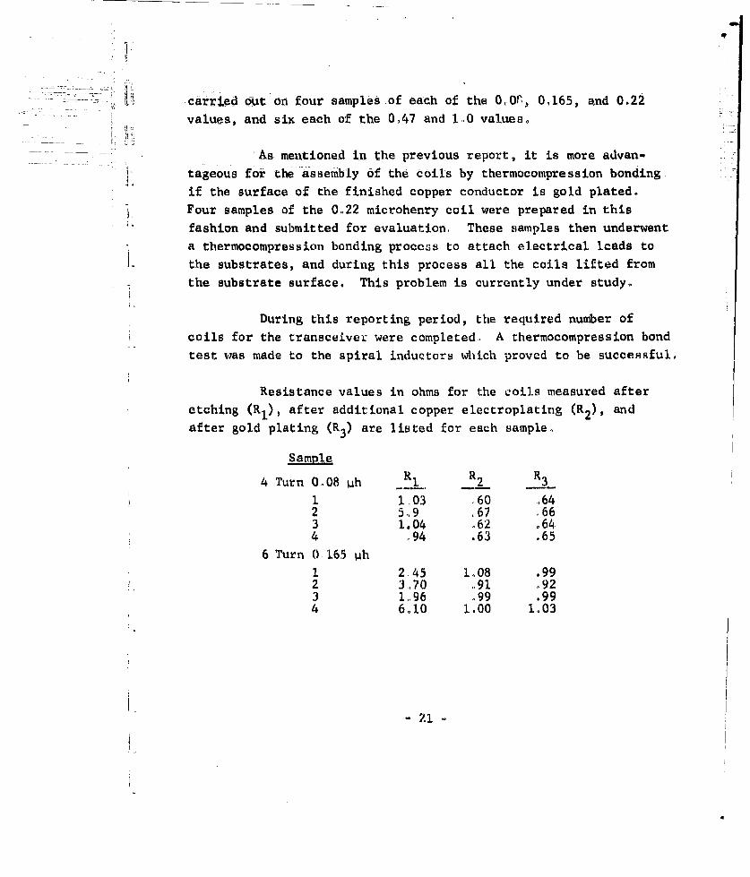
Resistance values in ohms for the coils measured afteretching (RI), after additional copper electroplating (R2 ), andafter gold plating (R3 ) are listed for each sample.
Sample
4 Turn 0.08 "h 1 2 3
1 1.03 60 .642 5,9 .67 .663 1.04 .62 .64.4 .94 .63 .65
6 Turn 0 165 ph1 2.45 1.08 .992 3,70 .,91 .923 1.96 .99 .994 6.10 1.00 1.03
- 21

• : i /7 Turn 0.22 ph1 2.05 1,.00 '98
S- 2 3,,60 1.02 1.023 2.,80 ,98 o99
. -... ... . .4 2.80 '190 .9114 Turn 0.47 ph
1 8.60 2.23 2..272 9,50 1.90 1.873 5o40 2.08 1.764 3,45 1.80 1.845 2.90 1,76 1.776 5.30 1i.90 1..86
19 Turn 1.0 ph
1 5.60 2,85 2.014.30 2.04 1.96
4 -5-30 2.03 1.985 4.80 2,30 2.256 4.00 2 20 2.10
(#2 lifted from substrate after etch)
A summary of the six principle steps in fabricating these
coils follows. The .ubstrates were given a light polish and
cleaned by ultrasonic agitation in acetone.
1. Vacuum deposit chrome-copper films.2ý. Successively electroplate and polish until a
smooth surface is obtained.3, Photoresist, expose, develop and etch.
4. Clean off photoresict and attach substrate andfilm with silver paint to approximately onesquare inch evaporated copper film on glassslides,. This slide area serves to reducecurrent density over the coil surface forsmoother plating.
5. Electroplate until desirud resistance value isobtained.
6. Clean off excessive copper deposit and silverpaste, and gold plate surface by immersiontechnique. Record final resistance value,
- '9 -

1
Until further samples are requested, no additionaleffort will be spent on this phase of the project.
3-4 Silicon Monoxide CapacitorsS'1
Investigations of the electrode materials used for thecapacitors and of the effects of the partial pressure of oxygenpresent in the vacuum systems during the evaporation of siliconmonoxide dielectrics are continuing, Results to date indicate thatunits fabricated with gold electrodes and with oxygen present inthe vacuum system during evaporation of the silicon monoxideproduced capacitors with the best life characteristics, A groupof 12 units of this type have been fabricated for an aging studyof encapsulated gold electrode silicon monoxide capacitors. Theseunits showed a 92% fabrication yield, and consistenL leakages forcapacitors of equal area.
For optimum results, it is necessary that the substratesonto which silicon monoxide films are deposited be preheatedbefore evaporation., During this reporting period, some experimen-tation was done with the geometry of the preheater in the vacuumsystem, in an attempt to obtain more efficient preheating of theeubstrates, Previously, this p'cheating was accomplished bysuspending a heated metallic strip in close proximity to the backof the substrate, resulting in the substrate becoming hot due toradiated heat from the metallic strip.. An attempt was made toplace the metallic strip in contact with the back of the substratein order to obtain more efficient heat transfer, but the resultingfilm showed evidence of large temperature variations over thesubstrate during evaporation.
- 23 -I[
!
, Durin the next period, life tests will continue on
-silicon monoide capacitors with various electrodes and various
deposition parameters. In addition, aging and environmental tests
of the encapsulated gold electroded capacitors will begin.
The aging and environmental tests initiated on a groupS* of 94 silicon monoxide capacitors during the last reporting
period were completed during the current period. An additionalquantity of silicon monoxide capacitors with gold electrodes were
run following the initial life tests., While the initial tests
were run at a temperature of 125*C, the second group of tests was
run for 48 hours at 125C followed by 240 hours at 85*C. All
capacitors in both groups were electrically stressed at 12 VDC
I throughout the tests, The results of these life tests are given
in Figure L,. On the basis of these tests, it would appear that
encapsulated silicon monoxide capacitors with aluminum electrodes
have the most favorable lifetime characteristics.
3.5 Tin Oxide Resistors
During this reporting period, a series of aging studies
was performed on a group of tin oxide films dcp~osited on both
glazed ceramics and passivated silicon substrates., Agingcharacteristics of the fifms at temperatures of 20'C, 60*C, 125%C
and 150%C were measured,. In the higher temperature ranges, aninitial decrease in the sheet resistivity fn the tin oxide films
was noted, followed by an increase with time to a value higher
than the initial resistivity. This aging effect is inversely
proportional to film thickness, i.,e., the thicker the film thesmaller the variation in resistance over a given period of time,
24 -
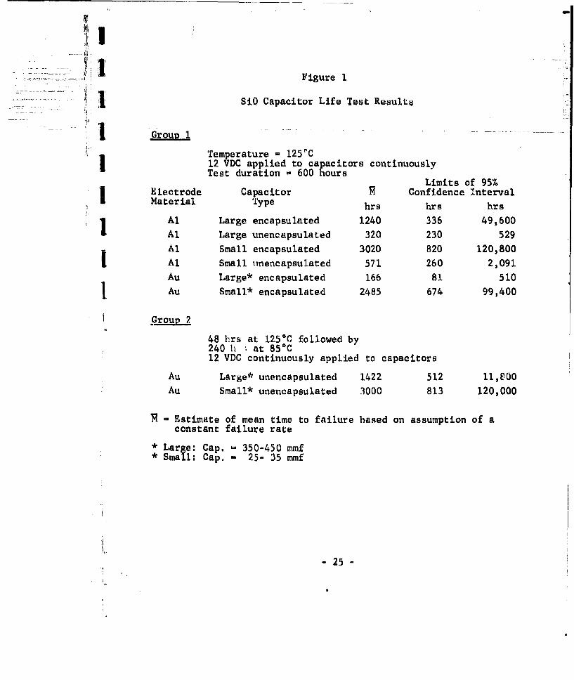
1 Fig ure1
i SiO Capacitor Life Test Results
I Grout) 1
Temperature 125rCI 12 VDC applied to capacitors continuously
Test duration 600 hoursLimits of 95%
Electrode Capacitor Confidence IntervalMaterial Type hrs hrs hrs
1 Al Large encapsulated 1240 336 49,600
| Al Large unencapsulated 320 230 529
Al Small encapsulated 3020 820 120,800Al Small linencapsulated 571 260 2,091Au Large* encapsulated 166 81 510
1 Au Small* encapsulated 2485 674 99,400
Group 2
48 hrs at 125*C followed by240 h , at 85*C12 VDC continuously applied to capacitors
Au Large* unencapsulated 1422 512 11e,E00Au Small* unencapsulated 3000 813 120,000
!- Estimate of mean time to failure based on assumption of aconstant failure rate
* Large: Cap. - 350-450 mmf*Small: Cap. - 25- 35 mmf
- 25 -

*1 i
The aging results at 20*C showed no discernible trend,the magnitude and direction of change in resistance varying from
o e film to the next, The most consistent results were obtained
from a set of substrates aged at 12500, Here the direction of
resistance change was consistent for all five films with only the
magnitude varying with film thickness.
"Further investigation in this area is warranted before
conclusions can be drawn from the present data.
During the next period the aging stability study will
be concluded. An attempt will be made to detect the characteristic
resistance (resistivity) vs. time relationship using the aging
temperature as a parameter, Further, an effort will be made to
define the physical and/or chemical mechanisms involved in the
observed aging pattern of these tin oxide films.
Aging studies to date indicate a much higher degree of
stability in tin oxide films deposited on SiO2 passivated silicon
wafers compared to those deposited on glazed ceramic substrates,
The aging stability of films deposited on silicon is
increased by encapsulation with a Ti02 film,
Two sets of films were made to conclude the aging study
on silicon substrates. The films in the first set were encapsu-
lated immediately after deposition; the second set was aged at
125C for 24 hours prior to encapsulation. As a whole, the first
set of films was only slightly more stable than the second set,
(Experimental data are depicted on the accompanying figures, See
Figures 2 and 3. It is apparent from a comparison of this data
- 26 -

ENCm4P3LJLt.ED Low 7cp&,RgrudA riNv OCiOI RssisroRsSSt~erRqT,: -514 ýCO~irxo -S/J.cpN -,-
- - - - - - -
7Q 7es s -to1-"s.
Soo-
200-
/00
AG.JNGL 7rit (HouRS).
ID30 so 70 1100/IMS -27-

1 10 ENCAPSM LATED-Lo T EmpR,44riAc 7Ne Oxio. R.sS/SrOAS
-AGWO 2'1 HA'S. P.R~oR To NCvA PSqIL4 U 04'
'Ii IAIG.r #PATS io.CAr-;: .125C.l
s1 timx e us~
300 900 3
200

- 'that there were anomalous effects involved in the deposition of-tin oxide films on a ceramic substrate,
A further aspect of the relative stability of tin oxide
, on aging that came to light during this study was the effect ofencapsulation on the film resistance. All the films used in thisexperiment showed a decrease in resistance of approximately 10
to 13% upon encapsulation.
I.The aging studies to date have been made with pureundoped tin oxide films, since the aging characteristics of undoped
I films provide a sensitive indication of contamination of the filmsfrom substrate materials. Resistor films doped with such materials
j as antimony and indium are expected to have considerably morestable aging characteristics, and will be studied during the
1 following report4ng period., (See Figure 5 - 8)
3A6 Interconnection of Integrated Circuit Submodules
Present effort is being directed to three concepts of1
interconnection,
I) The submodules (functional electronic blocks)are stacked and encapsulated with wires protrudingfrom the edges of the submodule which are cut off
flush with the surface of the encapsulant. Aprocess for the low temperature deposition of thickmetallic aluminum films is being investigated,
which, if successful, will permit an aluminum filmto be deposited on the periphery of the encapsulatedsubmodules and photoetched leaving an aluminumconductor between desired points,
- 29 -
*1

AG. N,G EFFEcr4
___ ~~low. rWNoCRATUR~41IOW N ~ ir35d70 &I83TRAT 51O c COATrgo- ~IcON. _
Lr A q..n Thf'mPcRqTuiiv 12~5 C.7e;'~c _
1 J
-1 A
Ao.I:No. 1,,.mr (HouRs);-~~

A 7I7 A G /NEF I-~C Ts'
'I - Low TiMpPERATRupC l7Ox'ICRESSMAS-6--1N--TE:&L-zt OCoz~q'/I __ A3IN&TEIPeRATURE.~C
J o~oc -VS.___ _
10 _ _ _16 0Ro o

-- ~~~~~~ & L I N~ipp G4CZ deRs.r~
-qooo8sr7:(~'AZED Aq~uc
U-
.4roo
40zo0400a
- L. --- TIGURE 6 _

/Ofo A A& iG ErFE~r
* - Low TEMP.1ArTURE TUVCQXIOE REs~isTORS
j SL4BSTRAC--: &LAZED.CLR/VIA
8000
OiFll,
A AGýING riMC (HOWRS)
40 80 2.4~O ~ o ;too
I/.--33-m_ý

2C)0 AG.INO EPECTS
Low Zi.MPclAruPE 77N OXaDc RESIsro,9sI 5 edSiOTRATE: G7LAzXrjD CERAMI1C
_',-- I -- O'TfC- -F- A NG i P RA- ru-- --U-bc -E--15- --
4,000
40a 00 0z~
AG.IWG lM~ ~ 'FIGURE8

2) The submnQduIes are stacked and ercapsulted.as in the previous concept, but connections are
made by the use of metallic foil conductors,
3) The submodules would be mounted on multi-
layered etched circuits boards.
A procedure for depositing thin aluminum films bypyrolsis reaction is currently under investigation.
In order to evaluate the usefulness of the aluminumfilms as means of obtaining satisfactory interconnections betweensubmodules, a module consisting of six submodules stacked withtest thin film components is now available to attempt interconnec-tion by this process. The basic requirements for a substratematerial have not been firmly established Therefore, modifica-tion to the present module may be necessary once the parametersare firm. The basic plan for this concept is to deposit thealuminum on one surface having perhaps as many as 36 contacts.The desired pattern of interconnection will be masked off and theexposed aluminum etched away Multilayered interconnections canbe accomplished by coating each conductor layer with a dielectricfilm and subsequently depositing aluminum over the dielectricfilm repeating the above process.
The metallic foll conductor process is similar to theabove with the exception of the technique of laying down the foil,The foil 'is applied against a "B" staged film adhesive betweencontacts by a hot stamping process. The contacts are then connectedto the foil by an ultrasonic welding process,. Preliminary attemptsto determine feasibility have been only modera'eiy successtui,
- 35 -

The foil was applied- to -the module, etched, and removal was3 attempted by immersion in an ultrasonic cleaning tank, The
remaining conductor, however, was not uniform in width and had
very ragged edges, New techniques are currently under study,
Interconnection by a multilayered etched circuit board
is being investigated. The artwork for a prototype board is now
in the layout stage.3
l
1
i ~- 36 -

-n
.... SIL-CON- PROCESS AND IZNTEGRATEDCIRCUIT TECHNOLOGY
. 41. Epitaxial Diffused-Integrated Circuits
*4~.1,1 Optimize'd Structure for lntegrated Circuiits
"7 IThe attempts at reducing series nollector resistanceare continuing and showing progress. The method being used was3 discussed in the monthly status report for April 1962.. Aheavily-doped planar N-type layer is diffused into a P-type
3 substrate. The original and regrown silicon dioxides are then
removed and an N-type epitaxial layer is grown over the entirewafer, A silicon dioxide layer is regrown and the pattern forthe isolating P-type grid is formed in this Ide layer. AP-type diffusion through the N-type epitaxial layer is performed.
A photograph of a device after the epitaxial growth step is shownin Figure 1, Figures 2 through 9 illustrate a series of cross-
sectional views of a wafer similar to that shown in Figure 1.Figure 7 shows the depth of penetration of the N-type layer
(white) into the P-type substrate (dark region). The gross whitearea is the N-type epitaxial layer The registration of the
N-type diffused layer to the trace pattern left on the surface
after epitaxial growth is quite good.
A group of NAND-NOR logic circuits has been processed
through the step shown in Figure 10,
Another group of circuits expressly designed for
testing the optimized structure have been processed up to the
epitaxial growth operation These circi!its are shown schematic-
ally in Figures 11 and 12,.
- 37 -

FIGURE 1.
F IGURE 2
-38-

F IGURE 3
rIGUR9 4
-39 -

'F IGUE
I~ FIGURE 6
m40-

ILI
IFIGURE 8
-41.

t.
FIGURE
- 42 -

-* Diffusion of isolation channels
- ~--~----Foxide
N-typ . . -typodltim' .~.P-typo rfuine&
*-yp s-tyolct
*N-type (substrateo)
FIGURE' .10 1*
* , -43;

J.I
al.~
.**''* I E, ill ~
*~~~~~~ A. .~'. -.~ * -
.. : 113~'

I, , . ,J, .
a.,. ....� , 'I
I ,9
I'''''II,.
a,.I , ., I I
*�*�*a .aI.,.� 1n I . a .�.. *� ,.
It j�, I 'I
I .11*............................z I�*
I' 91 .
-� I, ..II I
I '*�I I,
I,
- , . . ,iI 1 4
.1'
'I -o *
j �8O ZOQ �OO� ZOO , ,,.,,� I.
I - � .,.,.. a
II
'li, 1 1 .
1.1 *. I-,
ii;-, I, '9
�AI j I, � I**'i�I� 7 a ,
9 I9�
- I.,I, till' I .� I
.1'
9.4 .... n. a r. a .�. ,� -. I *

4.1o2 PNP Integrated Circuits
III All attempts to make silicon integrated circuits in
the past have been limited to those using the NPN transistorsL as the basic device. Work has been initiated on integrated
circuits using the PNP transis'or structure,IThe geometry to be used as a test vehicle in this
I program will be the same high frequency transistor as used in theNPN circuit development, The PNP silicon transistor presents alarge list of problem areas which will have to be resolved,
However, the basic scheme of isolation to be used in the PNPcircuits is similar to that used in the NPN circuits.
The sequence of operations to be employed in the fabri-cation of the PNP circuits is illustrated in Figures 13,14 and15.
High resistivity N-type silicon is u-,ed as the starting
'I material. On this N-type substrate, a P-type epitaxhal layer ofapproximately one ohm-cm resistivity and a thickness of 20 micronsis grown upon the N-type substrate. An oxide layer is grown upon
the P-type epitaxial layer. The pattern for the isolatingN-type grid is formed in this oxide layer, and an N-type channel
j is diffused through the P-type epitaxial layer to the N-type
substrate.
The pattern for the N-type base diffused region isformed in the original oxide layer, and an N..type region isdiffused into the P-type epitaxial layer Tle junction depth
will be approximately 2.8 microns, and the surface concentration
- 46 -

1-,lob
• ~Cross-seooional view of integrated oirouit
'struoture using PNP transistors
' °, : Cros-etonlve r n aodcrLi
X-typoe
Epitaxial collector growth
- I
• I. .
.P-type epitaxial layer
* . .*. * N-type substrate
' 1 Initial oxidation
oxide_______
,. ,P-'typo
N-type
FIGURE"::": " " -4;7.w

I
i F4 Z file '~o
C° .
ye opitaxial layer,
I *
P-typo substrate.d I:
( )
Cr.3satoa vie of opiie ineare cirui stucur
* I
I,
~~~~~FGR 1,.4,•o1p••' '
Is*4
"S P-typ:e
., 1 * .4,,
, .o~ai1B~ S
P-bypo , susr ,
* I
+.-, ., .
-" -48- .. , .
11 l - I- - 4'.-- 8~ - S *

.4 7
N-typo . 4' ,
Metalized oirui
ohmici 'contacts . 4
NP.typa .
4* ,-,tyI
* S , .1
49' .

* Degener~ate X+ region formod in bass
region in PNP transistors
> -typo-*
*.* -type
%1

18will be in the vicinity of 101 atom/CC. An oxide layer isregrown over the base region during the diffusion operation. Thepattern for the P-type emitter is formed over the N-type baseregion, and a boron diffusion is performed such that a base width
of one micron or less is obtained. %
At this point, the wafer is ready for an ohmic contact
j oxide etching operation, However, the problem of forming ohmiccontacts with alL.minum on N-type silicon once again arAes.Aluminum dopes silicon to approximately 2 x 10¹⁹ atoms/CC whenalloyed. The base region is doped to 1018 atoms/CC (N-type).If the aluminum is alloyed to the base region such that a "regrowth"
layer of aluminum-doped single crystal silicon is formed, thecontact on the base region will be rectifying, not ohmic.
Therefore, a degenerate N+ region must be formed inthe base region, as is shown in Figure 16,
The masks required to perform all these operations havebeen obtained, and groups of wafers have been procer --I throughthe isolation channel diffusion.,
-4_.2 Bonding Reliability Studies
Measurements have been taken on 11 S10 2 capacitors,which have completed a storage life test of 1000 hours at 300"C.
The capacitors were the Si02 type with aluminum metallization.Aluminum wire, .007" diameter, was bonded between the metallizationpattern and the gold plated post of the header,
The primary purpose of this test was to determine theeffect of high temperature on the aluminum to aluminum bond,
51 -

3 Normal techniques which bond gold wire to aluminum metallizationare not reliable after long periods above 3000C, The results ofthis test are shown in Table 1.
After 1000 hours, units #6 and #7 were open. Later
I inspection indicated thaL the Al. to Au bond at the post was openwhile the Al. to Al. bond on the unit was good. These results
I" indicate that an all aluminum system would be more reliable afterhigh temperature storage. Devices of this type are now being
I constructed for testing.
Bonding Reliability Studies
HoursUnit 0 1000
1 33 32
2 38 35
3 35 344 33 325 35 336 35 Open7 34 Open
8 32 30
9 29 28
10 23 2311 33 32
Capacitance Value in pf.
TABLE 1
- 52 -

4,3, Diffused Resistc.r Temperature Coefficients
As discussed previously, the hole mobility in the
diffused area is the primary temperature depondent variable in thedetermination of the total resistance, The slope and magnitudeof this temperature dependence is a direct function of the hole
impurity concentration. Because the "ohms/sq." value of anydiffused area is also a direct function of the impurity concentra-tion and the mobility, the temperature coefficient of the unit
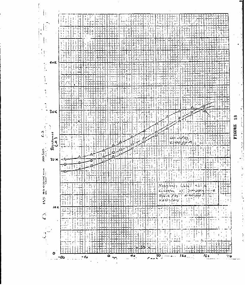
becomes a function of the "ohms/sq." This relationship is shownin Figure 17.
As indicated by theory and as shown in the above
- figure, the temperature coefficient of a diffused resistordecreases with increasing impurity concentration. A useful valueof resistivity is then in the range ot iUOi/sq, which results ina temperature coefficient of approximately 1500 ppm Mostintegrated c jices are now being designed using this value..
Figure 18 illustrated the uniformity of temperaturecoefficients for three 20 KO resistors, At 200n/sq., these unitshad a T.C. of approximately 2300 ppm. The. fall-off of the oneunit at high temperature was probably due to junction leakage.,
4-4 Metallization
A method of connection and interconnection of theelements in integrated circuits, The. immediate program is toprovide an interconnection of conducting paths between circtitelements which takes advantage of both intrinsic and extrinsicpaths. Metallization refers to the system and process of producing
- 53 -

~1 - 1 -4*-
": T
-~~ ~ -- - --- -
Al 4e5
- -2. - -_ - iitijjU
*- -- - - - - - - - -- - -- - -
IT II1 .
Io _
1h- mi11- 1IE1 1
""A.
'fl KARLl
TO-KK
ra - 1: :1 - 77 ' :' 'I 1I
lox.~ ~ I----------1 Lt
I T71, I
70Ii0JI[~ji V ______

the desired extrinsic interconnections. This metallized pattern
is to function both for interconnection of elements upon a
specific silicon chip and to provide means whereby connection canbe secured to the circuit environment.
In lieu of a more refined system with its subsequent
and necessary development time and in an endeavor to obtaininformation of circuit function at an earlier date the followingmetallizing scheme was envisioned and attempted. The method
- entailed a metallic pattern formed by photographic techniques
and provides contact islands to which thermocompression bonding
techniques could then connect to mounting assemblies such as
headers.IIn detail then, the wafer is prepared by conventional
diffusion and epitaxial processes to fabricate the active and
passive elements necessary for circuit function. After such a
procedure in general, the wafer and all elements are over-laid
with an isolating or passivating glass. Appropriate holes are
then chemically cut through the glass, utilizing photographic
techniques.
The wafer was then introduced into a high vacuum
evaporator and aluminum was deposited over the total surface toan estimated thickness of the order of 3000A. The vacuum
deposition was to a substrate whose temperature was not deliber-
ately alleviated in any outgassing procedure,
After deposition, the wafers were "photoresisted" and
etched to provide the required interconnection pattern. The
photoresist prevents etching where metallization is required.
- 56 -
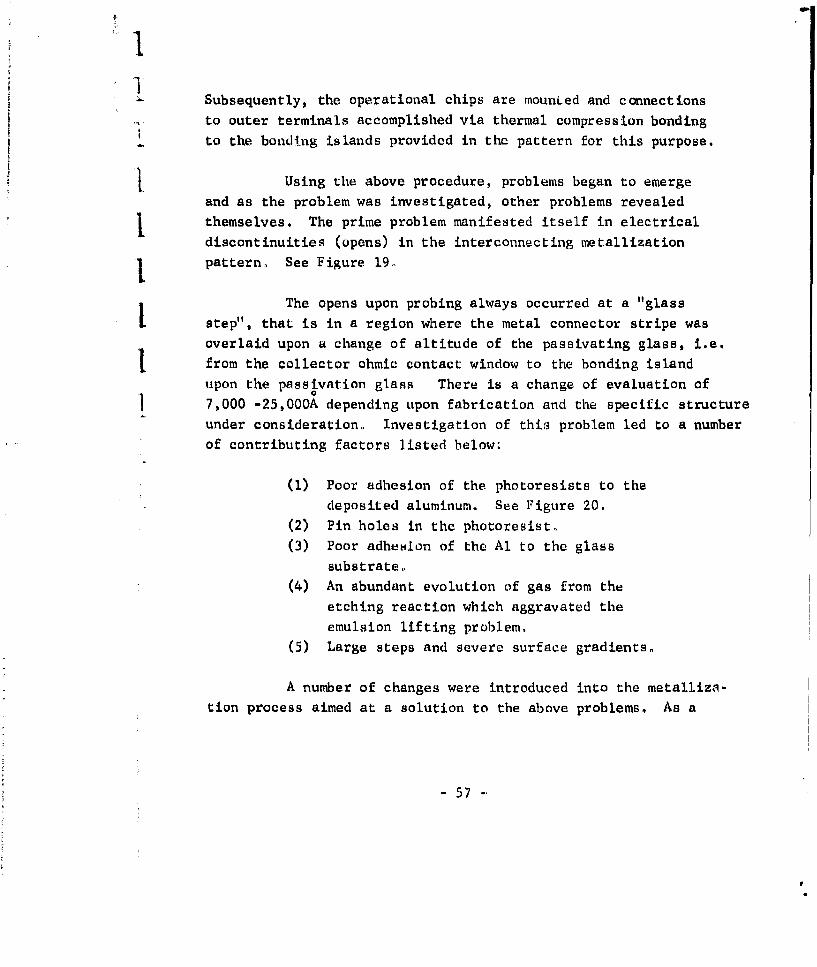
Subsequently, the operational chips are mounLed and connectionsto outer terminals accomplished via thermal compression bondingto the bonding islands provided in the pattern for this purpose.
Using the above procedure, problems began to emergeand as the problem was investigated, other problems revealedthemselves. The prime problem manifested itself in electricaldiscontinuities (opens) in the interconnecting metallization
pattern. See Figure 19,
The opens upon probing always occurred at a "glass
step", that is in a region where the metal connector stripe wasoverlaid upon a change of altitude of the passivating glass, i.e.from the collector ohmic contact window to the bonding islandupon the passivation glass There is a change of evaluation of7,000 -25,OOOA depending upon fabrication and the specific structureunder consideration., Investigation of this problem led to a numberof contributing factors listed below:
(1) Poor adhesion of the photoresists to thedeposited aluminum. See Figure 20.
(2) Pin holes in the photoresist,(3) Poor adheilon of the Al to the glass
substrate.(4) An abundant evolution of gas from the
etching reaction which aggravated theemulsion lifting problem.
(5) Large steps and severe surface gradients.
A number of changes were introduced into the metalliza-tion process aimed at a solution to the above problems. As a
- 57

iA
FIGURE 19
FI i
FIGURE 20
- 58 -

consequence, the process in detail is more elaborate, however,this is justified in the greatly improved results which have beenobtained to date. Most of the problems which appeared are well
in hand or have been virtually eliminatedý The only remainingproblem is the severe gradient in the glass topography; even herethe method while lacking elegance is an adequate one.
The current process is outlined below and a briefdiscussion of the pertinent changes and their relationship to theabove listed problems is included.
In essence, the general procedure is as outlined before,that is the metallizing is vacuum deposited in a continuous strata,selectively etched to produce the desired interconnection pattern.
In detail, however, there are a number ef changes.
First of all, the wafers are outgassed in high vacuumat high temperatures, secondly, the Al is deposited upon anelevated temperature substrate. These two modifications of theprocess are introduced to enhance the adhesion of the Al to thesilicon and glass surfaces. Quantitative numbers are not avail.-able, but the Al adherence is reflected, in that the depositedlayer can easily survive the difficult scotch-tape test.
The third innovation is a passivation of the depositedmetallic layer in atmosphere at elevated temperatures. Thefunction achieved here is greater adhesion of the photoresist
emulsions during the subsequent etching phase uf the process.
The fourth change has been in the photo emulsion itself,KPR has been used heretofore, primarily, because of its property
- 59 -

of being readily removed from the remaining pattern after the
etching has been achieved. KPR is known for its pin holing
difficulties, hence other photo emulsions were investigated.
It has been found that KMER could be removed adequately,
provided sufficient care is exercised in the photoresistive
preparation. Thus, with an emulsion change, the pin holing
problem has been alleviated, further since KMER is an acid
resistanL preparation and, because of the vigorous reaction of
caustic etches alternate etching preparations were given consider-
ation.
The fifth modification involves the etching prepaxation.
We have changed from a vigorour caustic etchant to a milder acid
"etch. The quantity of gaseous hydrogen evolved is reduced and
1 thus aids uniform etching. This seemingly of little significantfact is essential when time of etching is of sufficient duration
to degrade the integrity of the protective emulsion.
The sum total of the above changes is an interconnecting
1, pattern of very fine resolution. See Figure 21. In so doing,
the severe under-cutting of the pattern at a "glass step" is
I virtually eliminated. See Figure 22,
4.4.1 Contact Studies
1 As mentioned in previous reports, fabrication of
contact plates (or tabs) via photo-etching techniques have been
achieved. Since then, a metallization has been achieved in the
configuration also outlined at that time. Solderability of the
contacting photo to this pattern has been attempted, using
- 60 -

* /
I,1 IL .... 1
I.
K '1 I
Ii ,....* • m € ' • .. ... . ¶ ..
iiI. , . ' . ,.1 ' ,.
*1•'.,• '* • ./
• ; FIGURE .22.
',II P. ,d •, •.•
4\. .. ,
L'i . 6. =4

solders which have greater than 350 0C melting points. Optimizationof pressures and quantities of solders have not been yet achieved.However, soldering appears feasible. Sec Figure 23, Yield andreliability are, as yet, undetermined. Mechanical problems havearisen to how best to separate the interconnected pins withouttransmitting serious vertical stress to the contacting pattern.Some difficulty has thus far been experienced in the patternlifting from the glass. It has not yet been determined whetherthe metal to glass adhesion was poor or whether the stress trans-mitted was just too great; More work is anticipated in this area.
The details of the etching and evaporating process of
the aluminum metallizing was outlined in detail in the previousmonthly report. A considerable number of wafers have been pro-cassed by the technique And, in general, the results are gratifying.A "bug" appeared in a rather specific case and analysis of thesituation led to a slight modification of the operation, this
modification appears to have corrected the situation.
It was noted that in a certain circuit pattern which hadbeen processed within the glass etching phases in a manner whichdeviated from the routine method that these wafers had virtually100% opens somewhere within the circuit. Further study revealedthat all opens within a wafer had the common feature of beingoriented relative to the evaporation filament source. Introductionof a rather distributed source for the metal vapors such that themetal in transport came down upon the substrate in a randomfashion has reduced this problem. It should be noted that the
problem might not have occurred at all, except for the processdeviation. However, to insure safety of processing the conserva-tive step was taken.
- 62 -

I
I
1,
""' . , ~ AI ; ..\
'1.
IFIGURE 23
6
- 63 -

* ii.
* Related to metallizing is the placement of a metallic
layer upon the back side of the integrated chip or collection of
chips upon a wafer, Lu facilitate the bonding of the chip to asupporting substrate such as a header or ceramic plate.
The current method entails vapor vacuum deposition of
gold upon a properly prepared back side of a wafer. After a
wafer has been fabricated to completion, the gold is deposited toan estimated layer thickness of about 5000A, the gold is alloyed
to the silicon at approximately the cutectic temperature in an
inert and slightly reducing atmosphere. Normally, a bright
dendritic film of eutectic material is left upon the wafer surface.
However, a few wafers would develop what might be described as a
"rusty" surface.
At present, all experiments to control or even directly
effect the distribution or occurrence of this phenomena have met
with failure. The undesirable features of this "rust" may be
illustrated by looking at its properties.
*. The "rust" appears as a layer of material of unknown
composition which remains solid to quite high temperatures, even
in the presence of a Au-Si (Liquid) system. As such, it interferes
with proper chip to substrate bonding.
As of this writing, alternate systems of backing anddie bonding are under consideration and hence, if a solution is
not forthcoming, there remains the possibility of circumvention
of the problem.
- 64 -

4.4.2 Summary
The metallizing situation may be summed up as follows:
The evaporation and etching have been reduced to a routine
"process. With specific types of circuits some problems have been
encountered, these problems have subsequently been resolved,
!• I Related to metallizing is the backing of wafers preliminary to
"die" bonding to the ceramics or headers. A problem has
i developed and is now under investigation.
4.5 Testing of Monolithic Integrated CircuitsIFive monolithic integrated circuits have reached the
testing stage. These are:
1) IF Amplifier
2) NAND/NOR Logic3) Flip-Flop #1
4) Flip-Flop #25) Five Stage Darlington Amplifier
The testing procedure has been broken down into four steps.
1) Check for opens, shorts and voltage breakdowns.
2) Check of tolerance on resistors, hFE, etc.3) Check low frequency large and small signal
parameters,
4) Check high frequency and pulse characteristic.
The transistor curve tracer makes a useful tool for
steps one through three.
- 65 -

This testing procedure is coupled with visual examina-tions and visual defects are correlated with the electrical
measurements
Two circuits with visual defects are shown in Figures24 and 25. One is a Flip-Flop and the other a NAND/NOR LogicCircuit.
The most interesting test is the use of the "Black Box"approval utilizing the curve tracer as a four terminal networkanalyzer for "h" parameter measurements.I
The results of this work will be reported in subsequent
reports.
During the cuurse of this work, a suffic.'.nt number offully integrated circuits has now been constructed to developseveral methods of testing the completed units. In this type of
development work, a test should show three things:
1) Will the unit perform the intended function.
2) If not, what part of the unit is defective.3) If possible to determine, what is the physical
cause of this electrical defect,.
A, In the fully integrated circuits, as was discussed
previously, individual components tend to disappear into thephysical structure; thus, it is not always possible or practicalto check circuit performance by means of individual components.Two methods have been developed to obtain the required informationas discussed above, both of which may be considered as a "blackbox" type of measurement. The first involves checking the device
- 66 -

1
I f
__C-
FIGURE 24
IU I,•
FIGURE 25
67 -

characteristics between each of the external connections and the
contact to the substrate material. By the proper interpretationof each wave form, it is possible to analyze the performance of
the device. The second method consists of applying the operatingbias voltages to the circuit and displaying the Vin versus Voutcharacteristics on an x-y oscilloscope. This method indicatesthe actual transfer characteristics, although it is more difficultto analyze failures,
The first method simply con:;ists of a switching arrange-ment which places the collector and emitter connections of aTektronix 575 curve tracer between each external contact of the
circuit and the circuit substrate. The wave form is obtained
for both forward and reverse bias voltages and is compared to
those of a working unit. Figure 26 illustrates an example ofthis type of test on a fully integrated transistor diode logic
circuit.
This wave form may be compared to that of a working
unit or may be analyzed to determine resistor values, diffusion
concentrations and surface effects. In this example, the slopeof the trace indicates the resistor value while the break at -6
volts indicates the proper diffusion.
The second method is illustrated in Figure 27. The
circuit is connected to all supply and bias voltages requiredfor operation and a sweeping voltage is applied to the input.Vout as a function of Vin is shown on the Tektronix 536 x-yoscilloscope and the resultant wave form is analyzed or comparedto a working unit. Figure 28 and 29 illustrates a typical wave
form for the above transistor diode logic circuit. Tests of this
- 68 -

I r
] /7
/7/
II ///1
°1
FIGURE 26
ii./
Resistor to substrate test wave form of an integratedcircuit
Vert: 0.5 Ma/DivLsion"Horz: 2 Volts/Division
- 69 -

IIII
4 !
SWEEP Viri INTEGRATED Vo,GENERATOR CIRCUIT
S 60 CPS
Tektroniix .j36
Fig. 27'
Transfer Funotion Tout 0irouit
-70-

1L
*1
i FIGUR.E 28
1
L
F IGURE 29
- 71 -
nature would be particularly suited for production testing. Itshould also be noted that performance tests of this type may beapplied to any circuit whether linear or digital.
4.6 Optimized Structure for Integrated Circuits
The effort to reduce series collector resistance hasproceeded to the base and resistor diffusion operation. Severalgroups of NAND circuits have been processed through the diffusionand epitaxial growth cycles. The sheet resistance of thecollector region after epitaxial growth is sufficiently low toreduc.e the usefulness of these devices, the resistivity of anundoped epitaxial N-type layer being on the order of .02 ohm cm.The N-type layer is evidently being contaminated by the phosphorusimpurities in the N+ layer diffused into the substrate. Thesephosphorus impurities appear to diffuse into the epitaxial layervery rapidly as it is grown, causing a sharp reduction in theresistivity of the region.
An arsenic diffusion source should eliminate theseproblems due to out-diffusion of the N-type impurity. Thediffusion coefficient for arsenic at the epitaxial growth tempera-ture is 1.6 x 10"13 cm2 /sec. where phosphorus has a diffusioncoefficient of 2.8 x 10"2 cm2 /see. which is an order of magnitudehigher. Arsenic has a solubility in silicon in excess of 10atoms/cc, and will sufficiently "dope" the N+ layer to form ahighly conductive path.
. Ugh Frequency Integrated Amplifier
A group of high frequency amplifier circuits have beensuccessfully completed and are under evaluation in the transceiver.
- 72 -

This group of amplifier circuits represents the last of thistype until a redesign can be performed to make this circuit morecompatible with existing processes, Problems in achievingappropriate values for the collector load resistor due to surfacechannels on the very high resistance substrate and the low
collector voltage of these devices make its process undesirableat this time,
4.6.2 MECL Circuits
The MECL gates are being fabricated using the standardfour-layer device isolation scheme. Groups of units have beenprocessed through the base diffusion operation. These units are
illustrated in Figure 30.
"The MECL translator circuits have resistors only in theemitter circuit and a common collector, and may be fabricated asa three-layer device. These units have been processed up to the
emitter diffusion operation. They are illustrated in Figure 31.
4-6.3 Transistor Structures in Integrated Circuits
A complete evaluation of the electrical charac.eristics
of the NPN transistor used in integrated circuits has beenperformed. These units were fabricated on N+N epitaxial siliconin the planar structure. The electrical characteristics oftwenty-six of these devices is given in Figure 32. A typicaltransistor would have the following characteristics:
73 -

i LI -- <- '3 j
FIGURE 30
74

DEVICE/'Ae7-.ce*,Ar.'pu)gigars LOTN2 SC-104'
1 . 9) 1./ / ,1 .0 I /•.•1 •.4~ •w ,I •' .P . /-
L M 7I' "7.l 7e go A xg ..e , A ',1 -f- t i, le- 'A , x ."
-t,
2 .. 7.0L.L 2L ' Q 7u2! . 87/ ýl trJ~ L .. Le tL9 2 q -i. .ILO ol~ 2. 6 LZ .L. 67 L q ' __YI
g .. __. /.7.,/ , , .LL co' ýl",6 9. 1 67L ys 1 q ' 0-,
9 ' ',. 7 -1 W , 1 V 34-11 7f 4 2 - 1 6 . /7
A/, . 1 .1Of , 1,3/ fl, 690 $/ 2L l.... -',';.• 'Y• ,,7 . ._• ,/o e•/ .• :z.*' 7qV 0 • , -/7
NAM 7 -2 . J. -A .97 q 671 O 0 -0 /2
/ .. 9... . iZU . 32 . - 75 - -P -0/ 1r~ £l .Lq !2 Ye , 7 01 6,70
-L - - --7- -Y -.91 f 7. ? -4 -lv p.4 -q 1 -v.
F AVE £-NAME DATE 6 -MAP-OS
FIGURE 32 * 7

I VCE(sat) 0.2 VoltsBVcBO 60 Volts
- BVEBO 7.0 Volts
BVcEO 30 Volts
SCBO 1O0 Nano Amps
'CEO 0.5 Nano Amps* hFE 80
Cob 2.6 Pico Farads
Cib 3.2 Pico Farads
fT 650 Megacycles
rLc 45 Pico Sec.
The units were not lifetime killed, therefore, no switching data,maside from T on' was taken.
3 4.7 "Rust" Problem
The "rust" problem is under control and is currently
I not bothersome. An alternate backing method appears feasible,
and simply needs further development to establish itself as
I acceptable.
1 Concerning the aging problem of the Al-Au system has
related to wire bond strength - it appears that the problem has
been circumvented, in that Al wire has now been substituted forthe Au wire previously used.
A solderable contacts method has been accomplished upon
test patterns. The mechanical technique appears feasible on alaboratory basis. Evaluation using functional circuits is underway and the results will be forthcoming in the near future.
- 76 -

The "rust" problem as .utlined in a previous monthly
report is troublesome in that it makes die bonding much more
difficult. Various experiments, .iore completely adequate, have
]t beern designed in an attempt to iu-late the factors necessary toproduce the effect. A correlaticn has been observed and it is
f upon these results that the presert method of deposition is based.
It was observed that thoe wafers which exhibited "rust"jwere alloying to the Si substrate diring gold.1 deposition, This
alloying can be prevented by proper cleaning of the evaporation
system, such that radiation to the ,urface is limited, hence
substrate temperatures are held be!:)w eutectic temperatures.
Alloying during deposition may not be a sufficient condition for
rust, but it appears a 1)ecessary ole. F-,'ther studies along this
line have been postponod, b.-ue if other problems., Many wafershave been processed via the modifi,.d gold backing process over
the last two months without a,-tv evidence of the "rust" problem.
I jj It is the observatio'., which s':,porLs the idea that alloying is a
necessary condition
So, e work !-as been expended upn.:n an alternative backing
AI- alter......ve.ap avail2able, and i:T limited
numbers, has provided grattifying results Mechanically, the die
bonding is perhaps easier using the newer backing- This backingutilized Ni rather than Au, ".,Y, far, no plagues have appeared..
Further work is pla).nned with thi.s process before it will. beS I. adopted on a routine basis
As •.as kmentioned in a -previous report, the wire bonding
tecinique :.;a~s purely an expedient, and that the Au wire to Al
strip bond •-ws of a purely. tra.sistory n:ature It has no-, bee-i
-- 77

-par arpartially workedout ,The A wire can be read".ly substituted for
--Au, hence, eliminating the aging problem which occurs in a Al-Au
system. Although it appears that the problem Is not completely-eliminated, since if the header post are Au plated, the-problem hasonly been transferred to another area, This is only partially
* true. The rate of formation at the inter metallics is reportedto be accelerated at a given temperature in the presence of Si, so
* bonding to a Au plated post is somewhat less hazardous than to aaI wafer. Secondly, a layer of Au is not essential in wire bonding
to the header posts, hence the problem can be eliminated by usingother plating schemes on the internal header.
Solderable Contacts:Mention has been briefly made in prior reports that
solderable contacts are feasible., This is Indeed the case, in asmuch as metallized test patterns have been connected in a satis-factory manner to the pins of the 10 pin TO. 5 hender Joining tothe metal test pattern and again to the pins is accomplished bya high temperature soldering or brazing operation, thus producing
what appears to be a satisfactory mechanical and electricalconnection.
Feasibility has been demonstrated only at a laboratory
level. Samples fabricated to-date have not utilized any jiggingfacilities, These will be inherent in the process, however,
that the assembly will be self Jigging to a great extent. Thisis evident upon inspection of the "pin wheel," contacting platewhich is currently being used at this phase of the development.
78-

..8 Process Control
One of the basic problems in the production of inte-
grated circuits is the ability to successfully monitor the
processes involved and thereby achieve a high degree of quality
control. This problem is compounded by the fact that in inte-
grated circuitry there are many different circuits involved and
hence a standardized quality control process becomes difficult.
Since the basic sequence of processes involved in the fabrication
of any integrated circuit is somewhat the same, however, it
becomes feasible to devise a single control system which will
function for all of the various integrated circuits being
designed and produced.
During this report period such a single control systemfor use with all integrated circuits has been designed, and, as
a test pattern, is being incorporated in the integrated circuit
process.
4.3.1 Test Patterns
The test patterns are used for the measurement of
transistnr parameters, the quality of diffused junctions,
resistivity, alignment, resolution and many other measurements
needed for the close control of the integrated circuit process.
Thepattern is an integral part of the photoresist mask
and is positioned in the mask grid as shown in Figure 33. Using
the photoresist masks, the test pattern is formed on the wafer by
successive oxidation steps, As an example of the test pattern
-79-

7- 1
Test Patter'ns in~ Photoresist Mask* Figure 33 . .
4*. 1.4
Test Patterns on Water,�* Figure 34
9
80

concept, Figure 35 and 36 is an illustration of monitoring the
resolution of the photolithographic process. This control pattern
concept has been very valuable in measuring each diffusion and
masking step in the integrated circuit process,
4..2 Resistor Evaluation in integrated Circuits
The universal logic circuit of the type 705 has been
completed by using passivated-planar-epitaxial techniques.Functional characteristics are now being evaluated. This section
is a report on the resistor evaluations so far completed.
Figure 37 shows the locations of the points evaluatedon a 100 mil square die bonded to a TO-5 header. These points
were arbitrarily selected for evaluation; and the numbers in the
figure refer to the standard pin numbers of the header. The
resistors were formed in the circuit by P-type impurities being
diffused into an N-type isolation region on a P-type substrate.
A three dimensional sketch is shown in Figure 38.
The results of the evaluations for three circuits are
listed in Figure 39. The range of the percentage difference
between the design values and the tested values varied from 407.to 208. with a mean of 102%. A thorough check of the design,
process monitoring tests, and operations control is being
conducted. Improvements will be reported later. The normalized
variance with each circuit is plotted in Figure 40 for every
resistor tested. It appears that the 0.4K, 0.8K and 3.8K
resistances have a definite relatiqn to the designed value,
indicating in all probability, the process control was constant.
However, the 5.0K resistors have random values which implies the
81-

.. 2 A2
fU
Layoat~of Resolution Patterns
Fisuve 35
S- +82-

t%
83 N

design control was-not carried over to the high value resistances.
Temperature stability studies were investigated and
the results are displayed in Figures 41,42, 43 and 44. The
temperature coefficient of resistance appears to approach zero in
the neighborhood of 220 K (-53 0 C). At lower temperatures the
temperature coefficient of resistance is negative; and at higher
temperatures a positive temperature coefficient exists. This
behavior is characteristic of the doping level of the scmicon-
ductors employed in the resistors measured. The thermal
coefficient of resistance was computed for each circuit from the
slope of the curve at 550 C. The values obtained from Figures 41to 43 inclusive are shown below in Figure 45. Essentially,circuits B and C have identical temperature coefficients.
Figure 45
Some Thermal Coefficients of Resistance
Coefficient of Resistance at 55*C
Circuit A 4410 ppm/ 0 CCircuit B 2060Circuit C 2050
Avcrage 2840 ppm/*C
This similarity agrees with that obtained in Figure 40 and again
indicates the consistency of the design to control the resistances
measured. Figure 44 compares the measured resistances against
the designed values. The two curves are in agreement below 60 C
(1400F).
-84-

IFIRI L13
u AW
00
IJ i [E0iE lOE
Fi~gum37Tygo75Unidversal Loglo Ciroultas de.fro Resistor' valuation

Ii
A Typical P-type Resistor Used in Integrated Oraouits
Base (Resistor)
Oolleotor (IsolationRegion)
S- -Substrate
4. *

FIGURE 39
Resistor Value& of an Evaluated Integrated Circuit
SResistor Cirouit Desired Measured Per Cent NormalizedValue Value Error Value
S1 -2 A 400 2 800 a 100% 200o
B 400 2 1230 9 208% 3089
C Loo 12302 208% 3089
Average 400 2 1087 9 172% 272 9
2 -3 A 800B 9 1090 9 36% 136 9
B 800 9 1670 2 109% 209 9
o 8oo._ 17709 121% 22192
Average 800 2 1510 9 89% 189 9
3 -4. A 38009 47209 214% 124 2
B 3800 9 7140 9 96% 196 9
C 38009 7350 22 9
Average 3800 2 6503 9 71% 171 2
6 -7 A 5000 79709 59% 159 9
B 50009a 111109a 50% 1509a
a 5000 9 9460 2 122% 222 9
8 -9 A 5000 9 75209 240% 140 0
B 5000 9 70009 89% 189 2
.o 5000 10320 9 U06206
Average 5000 9 8897 9 78% 178 9

Figure !_40_ .
Resistanoces Normalized with Respect to DesignObjective Values for the Oirouits Evaluated
LEGEND
2.80 0 Circuit A
0 Circuit B
7 Z.60 c ircuit C
HI
4• 2, Z0
S2.00
Rola•X. don~lf'..o4.7• g.
Ressto -nttiation

F r1 e__
Average Temperature Coeofioients
for Resistors in CirOuit A
/00o
'- SI
ID2 6
T r i
iZOO 9
,90 • -I II .. t I . i
•L-~o =-40 -ZO 0 .•o "0 dO 00 0 /•0 #*O
! ~~Temperatur~e in *0 ,
L.1

Figu•e _42_
"Average Temperature Coeffiotent "for Rusistors in O1.w0ul4 B
Z//C)44
MI
Vi
P2 '
/0
-60 40.-V 0 J ,0 60 ,A A 4
r i
01
45 Zl
.904 I oo // , .
-60 -,40 • 0 •o 04 6o. ,0 ,0 ,4o /
Tompol, atu. oin QO

/.,,FiPgu ,e;'•, ....3:. .. 2 '.
Average Temperature Coeffiioientsfor Resistors in Oirouit 0
Z.//N
.00
i/o,*¢1*
-60o -40 -&70 0 ZO '.,V 60. 40 /W AM A
Timpera t~ure in '00'
alf

S,.FIGURE 4 4 .,
Tempeorature Dependence of Resistance
4. L~ zo
I d
1 0
Na /.iO4,1-
H
.90 1. - . 1
LE T r
., 1 I l I I I
"1 -60 -,40 -ZO 0 ,? *' 60 80o #0 A /40
Temperature in 'C
0 Resistance Calculated from the Doping Impur'ityConcentrations, Used.
A Average Normalilsed"Resistance Measured In theThree Grut@

5.0 ADVANCED CIRCUIT DESIGN STUDIES
1 5.1 DCTL (Direct Coupled Transistor Logic)
I The 8-bit arithmetic unit and its associated printed
circuit cards are now completed. Since the printed cards were
I grounded to the rack at only one point on each card, considerable
pulse degradation due to ground loops was observed. This problem
was solved by installation of a more complete ground bus systemand clip arrangement to ground the opposite edge of each card.'1
The unit was checked for accurate logical operation.
"Then data was taken to determine average delay across each type
logic block. A Vcc of 5 v applies to the data given here, but
Sdelays varied only a few percent with Vcc M 3 Lo 7 volts.
3- or 8-input "OR" Gate - Av. Delay - 26 nsec
3-input "\ND" Gate - Av., Delay - 34 nsec.
7-input "AND" Gate - Av. Delay - 40 nsec.
Half-Adder - Av. Delay - 20 nsec.
It was observed that the lower half-adder of a given
full-adder had much more delay (f,20 nsec more) than the upperhalf-adder. This was due to the degradation of the output pulseof the single inverter being used to drive the X inputs of alk8 lower half-adders. The large fan-out at this node resulted insuch trailing edge delay as to give the lower half-adder theappearance of being much slowev, To eliminate this effect itwould be necessary to drive each bit's X input from a separateinverter.
" 93 "

Tests were made to determine carry propagation delays
of the total system in both parallel-parallel and ripple-carrymodes. These tests were made as follows: The Y, Y inputs were
made static DC. The X, X inputs were pulsed with an E-H Research
Labs Model 131 generator. The inputs to bit 1 were X + 1
(pulsed), Y - 1. All 7 other bit inputs were made X 1 1, Y - 0.
Thus, a carry was generated in bit 1 and propagated to the bit
8 carry output.
L
Data given is only for leading edge delay. Because of
the test set up described, the trailing edge of the bit 8 carry
output was triggered by the X.-input pulse's trailing edge being
propagated only through the bit 8 full-adder, Therefore, the
trailing edge is of no significance in determining delays of the
total system. This is the case in both ripple and parallel-parallel operation.
Propagation Path =ein to eighth bit carry output
MODE Vcc LeadinA Edge Delay
Par.-Par, 3v 77 nsecRipple 3v 204 nsec
Par.-Par, 5v 70 nsecRipple 5v 191 nsec
Par.-Par. 7v 72 nsecRipple 7v 203 nsec
A detailed observation of slivers was made, These
slivers usually take the form of short spikes in the sum or carry
outputs of higher-order bits when these outputs should logicallybe zero. They can be identified as occurring at times when theoutput pulse would he rising or falling if an output pulse werepresent.
- 94

t
Slivers of this type were found to arise from two effects:
-11) Unequal delays on inputs to "AND" gates, resulting
in short"time gaps" in the switching period during
which no input is as high as the threshold voltage of
the input transistors. This effect is observable,
. although not so great, even if all inputs are "in phase"
since even then one input may fall below VT before
another input rises to VT-
2) Unequal delays on inputs to half-adder. This is the
inevitable result of the fact that some inputs must pass
through more logic blocks than others.
Another effect which might be termed a "DC sliver", is
seen in the half-adder sum and carry outputs if the DC X, X is
slowly varied while Y, Y is held static, There is a very narrow
range of em for which a sum output will be produced. Assuming
all devices in the half-adder are identical in other respects,
* this range of en is a function of the difference between the thres-
"hold voltage of the device fed directly by X and the threshold
* voltage of the inverter which drives the Y input.
During the next period, the entire 8.bit arithmetic unit
will be tested at high and low temperatures, and results compared
with those obtained at room temperature.
5.1.1 DCTL Current HogginR Analysis
The dependence of DCTL design on device parameters has
been partially investigated. The parametric equations derived by
- 95

Ebers and Moll were used to determine the variation of circuit
voltages with a variation of device parameters.
The number of transistor bases that may be connected
to any given voltage node (fan out) is greatly curtailed by the
variation of the different transistor input characteristics.
V rblb + 0 BES + (Ic + Ib) rE (i)
L r; - base body resistance
rE - emitter body resistance
0 OBES - base to emitter junction potential
I VAES - VBES (Ic + 'b) rE = rblb + 0 BES (2)
0 BES m.!LT In I b+ (1 O'd c" (3)q L TEO
a- inverse alpha
IEO base-emitter leakage current
The change in the input characteristics from device to
device can be examined by setting 1c and Ib at a constant valuein equation (2). Here we have::
VE , K, + in 1 + iT In (1 + (1 -cL) K2 )BES b q 1 0
The controlling parameters in this case are IEO; r' and aI.
To make the device parameters least effective in varyingthe input characteristics, the addition of an external resistor in
"0 series with the base is necessary.
- 96

Y
The input characteristic on collector current can bedetermined by defining a change in base-emitter voltage as a
function of the change in collector current.
LVBESJ _ KT leo _I)S.[Ic .] q leo Ib + (1-aI) 1c
a lim VBES KT 1
I>0 'Ic q Ib + Ic
lim VE_ S -
dVBES KT (I -aI) dl
VBE iq Ib + (1 -ai) Ib
AV KT ln Ib + (1 -al) Ic 2
From the above we see that in the limit of high a,, we
"have little dependence of the input characteristic on collectorcurrent. This is indeed the case, and high values of inversealpha are beneficial if the value of alpha can be closely controlled.
L2 HECL
The piece-wise linear analysis technique was used for
the st-ady-sLaLe design ui L.he basic ?ECL logic block.
- 97 -

Several multiple chip MECL circuits have been received.Preliminary data indicates no observable degradation between the
breadboard circuit and the multiple chip circuit. The printedcard layout for the 10-bit MECL adder is about 50W complete.Layout of MECL is somewhat more difficult than the DCTL layout due
to the number of power supplies. The multiple chip circuits arebeing used since they should be a closer similation of theintegrated circuit than the printed circuit type used in DCTL.
The arithmetic adder should provide a good comparison
of DCTL, MECL and DTL under dynamic operating conditions.
*5.3 DTL
During the quarter, work on DTL has uontinued, withemphasis placed on measurement of switching times for variouspower levels, impedance levels and configurations.
Figure 1 shows switching time vs. power level measuredfor three of the most important possible configurations obtainable
in DTL. The data was obtained by varying impedance level in achain of DTL devices built up in discrete form as shown inFigure 1. This chain represents the "ideal" case in the sense
that each module sees only a fan-out of 1.
Figure 2 shows a similar curve obtained with lOpf
* capacitors added as shown to simulate fan-in and fan-out lineloads.
A "research vehicle" DTL circuit was designed and
submitted for device fabrication. Figure 3 shows the predicted
" 98 -

worst case" fan-out vs. power supply voltage and tolerance fortypical environmental conditions. Figure 4 shows measured
average propagation times for this circuit vs. power supplyvoltages obtained using discrete models of this circuit. Heavyfan-out loading was simulated by adding 150 pf capacitors fromoutput collectors to ground to the circuits shown in Figure 3.
An interesting comparison between DTL, MECL and DCTL isshown in Figure 5 where average propagation times vs. power levelmeasurements for nominal models of the threeo logic schemes havebeen consolidated. The data shown plotted in Figure 5 was not all
"-) taken in the same manner - impedance levels having been changed
for the DTL and MECL curves and power supply levels for DCTI.
Analytical work on DTL continued with emphasis being
placed on the design of an optimum wafer which could be used withdifferent metallization patterns to obtain leading edge triggered
flip-flops, trailing edge triggered flip-flops, and numerous"NAND"-"NOR" logic gate types.
Figures 6 to i0 show the results of DC Worst CaseAnalysis and propagation time measurements made for two discrete
versions of research vehicle NAND circuits that are under consider-ation. Note that diodes have replaced the multiple emitter inputtransistors used previously. This design change was institutedwhen measurements of the multiple emitter design under similatedfan out conditions revealed that the inverse beta of transistors
in the fan out stages was causing excessive loading of the drivingstage. In fact, it was discovered that even though the inversebeta was very low (less than .5) in the 2N834 devices used, a fanout of one was sufficient to keep the collector of the high
99

impedance design from returning fully to Vcc when the outputdevice shut off,
Design work on the DTL optimum wafer has produced an
interesting possibility. Figures llthroughl4 show how one DTLassembly could be used for five different circuits by merely
changing external connections, Two types of flip-flops can bemade by cross coupling two of the DTL devices as shown in Figures1i and 12, The five input "NAND" junction can be obtained using one
device as shown in Figure 13. The multiple diode assembly as shownin Figure 10 could be used to increase the fan in of the fiveinput "NAND" of Figure 13.
An alternate way of obtaining the functions desirable
above is also being investigated, This technique will use a dual"NAND" in each device and use different metallization masks toget the desired interconnections.
The leading edge and trailing edge triggered flip-flop
designs ats shown in Figures 11 and 32 were tested extensively indiscrete form. Switching performance was found similar to theDTL "NAND" gates, with total transition times equivalent to the
propagation time for two stages of "NAND" gates. Repetition ratesof up to 10 mc were observed for the toggle or "I' flip-flop
design.
_100"

..... .. ,. T 1 -r' .stll~A":' U2
N, d
. .I 1. I I Y 1 .. ...... F ~
oili
. .. ... .... .... . .. . .
. .. .....
K~~~~~~F A77- ~~nJ /U~47$FI~uRE1
r4a

AV..
Li.t
'I--I-. .. ..........
I.o I.
17 IN
-1 W! 2.
71m 41 A1 ,
/h'c~ ~ ~ ~~~-, r ~*l ~d i lAf*AIUR I 2; .t . ...

I.Fj ITilIT V
It IIto
kjib
1444V .y:1u.44
'I w x 'Iq t1
7$ .~ j ~.44.L;VV__
vat2'? '~ ;;.'j~i....~,r. r AV' 2. :2
'-1' ~~* **7e7~. ~I ;
j~. j~'~
*~~~FGR 3 .*..I &14

Ai I
A. j.. J. .~±t t*V~4
47 ...... ...
w 0sjji ~Ls 1t't
-4~4
1" 1-99
T. I

iI Pi..H1 A
11ti Tolc NO . P'1W ..h ... .. I I
7.-- -- 7
4J-rI 10JJ
44 F
W, In
I4H .2. Vl l'r ........
63 I r
FIGURE; 5

1~TM! -I -~ 7 1TM T . .1-! 11 TTTiI hf Y~~ T 2iW
(I Hi 1! -! 1 11111 11hI 4v V o L
ii;4::itt,' q flh
h~ li Ill n * II~
'' I J il l
I:It
T !i, iIl~
'i ;14 fi tII I~~r'lI il y~.~C/?L~()II m6
-106-

C jfi tI; 1 ~ ILI :.! U411K'
.A .f4 TT U. li e It 'ii~~!, f I I ~oil Iii 1
it I f I Il
1!II i II.II
i
1 01
ITI
£01
ASSOMPTIONS IN WORST ---CASE -j~AL\L-,IS:Uise. of 2?N834- Type Trr'nsis+oY%
VGT( r) .73 w v. I~~ei j101v~ a d .- OO voNS/1"C Thnej' CdcŽ.)
Vsrsr) -~~737v .603V
V.r(s'd) lV. (aidewiny 1 0,% f/yedd) +i,00o34 1~i/011 TeiMP. tcoi.~)
Averaqe Cor4i/n~ o~o-" aaV Hs (4dtOWin9 10%/Vcoj-U2 "'y/o'e Tm-ny.
___:Col(p.)__ +Pas -Driye QlcideC
Avemp~ coflad;Zt-fl 01op...6voth (allowing 10% vayed1;-.JO?2. vad/'Terti. COO.~)
Coo!1 (241'e3 .15 S'
.11/0/0(. Tomp COrFFcie,Rt; Vrtawtior -Amm' !9d Trepv 0.5'e) 206 Coo<)'± Z. d% Re~s ec-ivi`y isvor per wscfor
MOVm Woe )~Ma MI
D"n201 ma~ Up !(0) Wflir hown 2,01 W~rf
_MA4 MII MA1' ~As Mi~i M~11 'AX M
1K~ 1.245 1.205K_ 'LK 6.03~gK )2.15K1 4J.5K f .1S/ 7SNI ~ ~ ~ _ý _3 ~4 102 ý LT..ov.j!\ *.'71 ý, s'7s x 9 a!
Up .~ 20IlI ~.Lyq3 2.IDr WaterI' 3Do",~a 2 W* AcI.VUUE if
F) CUR E.
HI
~~ILI
0 I Ii qI t1
Ei' I
N i I I'I i I ' $
I' II 1 I 1~''l o 1h*Iu'1iinllI :' ~ ~10.

,It : 1 it I~ f i i
ItI
liii: Nl II I
II~~;I litII'' II
NI 1I
hi I hi
:I I 1 1 It I I il t 1I i : 1 1 !iII
ILI~ Ii 4 4 L J
III
1141
ti110,

v I X c., IC
I.A
L1U
"IL

L • U
l I
-. 4 ki
% I
* -' .II
.. .
L Id
tu
IL ILrs IO 1I ~ Iic
112

6.0 UHF TRANSCEIVER DESIGN AND FABRICATION
6.1 Fabrication of Hybrid Integrated Circuits
The various hybrid integrated circuits for the trans-ceiver have all been completely designed and most have beenfabricated in sufficient numbers for several models, These includeredesigns of several stages for various reasons. For example, thedetector and AGC stages have been completely redesigned to elimin-ate some leakage currents which developed in the filter capacitorzener diodes, making the stages operate poorly in the receiver
1,. model.
Apparently, this increased leakage is due to partialdegradation of the diode junction, due to partial alloying of goldwith the silicon, during the strap-bonding process.. A slightincrease in leakage current is not especially intolerable in thecase of the grounded bypass capacitors in the regular linearamplifier stages. In this particular case, the combination of thehigh value resistors in the AGC filter with the leakage currentcauses an objectionable load on the AGC signal.
The high frequency stages (120 Mc RF and 108 McOscillator) have been redesigned arouad the new ultra high frequencytransistor recently made available. This provides 10 db more RFgain and higher oscillator stability than in the original stages.
The new RF stagqs, including those in the transmittersection are being fabricated with the RF capacitors within theTO-5 can.
-113-

Some spiral inductors recently received from the
Motorola Solid-State Division now appear to be able to withstand
the required bonding temperatures, and some 108 Mc oscillatorunits are, at present, being built with integrated inductors inwhich the only outboard component will be the frequency
controlling crystal.
Some experiments are also underway in mounting some very
small toroid inductors within the TO-5 can in assoctation with a-circuit.
The audio amplifier stage, which was described in aprevious report, has proven to be unreliable from a fabrication
standpoint. The problem appears to be that the Darlington voltage
amplifier requires careful balance of the input base bias. Since
our best resistor tolerance at this time is +10%, with some localvariations outside of this limit, this delicate bias adjustment isnot always obtained, resulting in a large percentage of stages
with poor operational characteristics.
It has appeared worthwhile to redesign this stage also.A similar less critical circuit has been developed which will be
* more reproducible, and provide better gain with less distortion.This stage will include a direct output into the new offsetreceiver transducers recently received. This approach eliminatesthe necessity for a large coupling capacitor from the audio outputinto the speaker.
A schematic diagram of the improved audio amplifier isshown in Figure 1.
114 -

Id. 62 7 A14010 AIA-f ,?fDe%5161A
7.11
0 ka
L * for
ido *C
O.9
ýIGURE,.
Speaker.,

6.2 Crystal Filters
One of each of the 120 Mc and 1.2 Mc crystal filters have
been received from the Chicago Motorola Communications Division.
These units have the four-crystal filter network mounted in TO-5
cans, but other com~ponents, such as resistors, capacitors and
toroid inductors are mounted outboard, We are conferring with the
supplier on the possibilities of either further concentration of
elements, a slightly larger container, or a two-can all-internal
mounting.
SCIn all respects, these filters operate very well, and
have been added to the interim circuit board model,
6.3 Inductor Development and Other New Hybrid CircuitElements
Inductors for the hybrid integrated circuits so far
developed all take the form of a spiral deposition of metal on aceramic substrate. This substrate occupies one layer on the TO-5ten pin header.
These are made by the Motorola Solid-State Systems
Division by thin film, masking and gold deposition techniques.
In the first samples received, the metallization lifted off the
i highly polished ceramic substrate in the wire bonding procedureat the temperature of 350'C,, Later samples made on unpolished
ceramics have proved more temperature sLable, and these will
probably be suitable for Integration into the cans.
Some experimental inductors were made in our own facility
by a silk screening process, These have excellent adherence to
-116-
! ithe ceramic, due to the sintered moly-manganese metallization.
Evaluation has shown that these have only an average of .03 uh.
I' This is due to the very wide spacing between turns, required by
the tolerances presently available in the silk screening technique.
I These are not, at the present time, suitable for use in the
transceiver.
I Several relatively new elements for hybrid integrated
circuit structures have been developed. These include the
dielectric capacitors. These capacitors are formed on very lowresistivity silicon substrate with oxide coating. The upper
I capacitor plates are deposited aluminum. In one form called the
binary capacitor, areas are increasing by doubling, which can
I provide any capacitance between 2 and 254 pfd in increments of2 pfd, by suitably connecting the top plates..
1 These capacitors are especially useful in high frequency
circuits, where junction capacitors, such as the zener diodes or
other p-n junction areas will not perform satisfactorily.
A photograph of the top layer of the redesigned 120 Mc
Mixer stage (624) using the new UHF transistors and binary
capacitors is given in Figure 2,
The UHF transistor is a new design which provides afT
cutoff frequency of 1000 Mc or more. This provides much more
gain and better performance in high frequency applications than
the 2N834 UHF transistor used up to the present time.
Another new element is the planar passivated zener diode.
This device will have several advantages over the standard zener
- 117 -

U
I\
1 /
FIGURM 2
Redesigned 624; 120 Me RP mixer stage includingUHF transistors and binary RP capaciStors.
-118-

II
F IGURE 3
Partly assembled interim model Transceiver Circuit Board
-119-

F
v diode dies presently used in hybrid integrated circuits. Theoxide passivation will, of course, provide cleaner units in all
cases, and the aluminum metallizatLion will provide bonding withoutthe risk of gold alloying. These will be provided for fabricationof hybrid integrated circuits in the near future,
An additional new electronic component is the offsethigh impedance miniature speaker. This has been designed by the
vendor for coupling directly into the audio output circuit, thus,eliminating the 5 ufd coupling capacitor, The DC amplifier current
pulls the diaphragm to the center and allows full diaphragmexcursion without any limiting.
Interim Model Transceiver
Circuit boards and a containing package to house acomplete transceiver model has been designed and the hardwarefabricated. The package includes all peripheral equipment,batteries and collapsible dipole antenna,
One model has been assembled on this structure. AtpreRent, this model contains the complete receiver section and thetransmitter section will be installed very shortly.
In the assembly on the circuit board, shown in Figure 3hybrid integrated circuits are used throughout. Some of thesestages, notably the RF and crystal filter stages require someoutboard components. New designs of some of these units as
- 120 -

discussed elsewhere in this report, will greatly reduce this loadof exterior components,
These new hybrid integrated stages will be designedonto a new circuit: board with reduced dimensions, This latterdesign will be then approaching the final model.
" - Further reductions in size may be effected when single
block integrated amplifiers and other circuits become available.
The overall size factor may be substantially improved by the
adoption of the new flat package which has been proposed.
6,5 Hybrid Integrated Linear Amplifier
The fabrication experience of the hybrid integrated
circuit units for this transceiver development, has indicated"that certain of these units can be produced with a relatively
high degree of reproducibility. This is especially true of several
of the units used as IF amplifiers in both the 12 Me and 455 Kc
sections.
These units may be cascaded together along with crystal
or ceramic resonant filter elements to provide IF amiplifier stripsat several useful conventional frequencies..
Since such strips may be of quite wide interest in many* areas, some preliminary evaluations have been made on these
* .cascaded amplifier strips.
Two hybrid integrated linear amplifier circuits we havedeveloped, appear to be useful on a general purpose IF application
basis. These are;
- 121-

(1) The H.I.C. 640 Fixed Bias Stage as shownschematically in Figure 4. This is a perfectly conventional
voltage amplifier stage with built-in emitter bypass and bothdirect and capacative collector outputs available
1.
(2) The H.I.C. 631 stage, provides the same features,in addition to an isolated base input network for the injection ofa D.C. bias voltage from an external, source, This external sourcemay be derived from a volume control, AG.C,. or other sources.
At maximum gain (about 1,5 volts positive on theinjection network), this stage has essentially the same frequency
and gain characteristics of the H.I.C. 640.
Some of the performance characteristics so far evaluated
on cascaded strip amplifiers composed of these units are summarized
in Figures 5 and 6,.I
Figure 5 shows the gain vs frequency for a single 640
stage when loaded with a following, cascaded 640 stage.
In this curve the low frequency fall off is due to the
limiting aspects of the emitter bypass capacitor value. In theregion of 455 Kc to 1 Mc the per-stage gain is better than 25 db,falling off to 11 db at 10 Me. Anywhere in this region the gain
is sufficient to be useful in practical IF amplifier strips,
Figure 6 shows the overall response of a two-stage IF
amplifier with a series resonant ceramic 455 Kc filter. TheH.I.C. schematic of this circuit is also shown. The 661 stage
is a commercial ceramic resonant filter which has been mounted ina TO-5 can.
122 -

II
44 0014d
0 Ism
FIGH. 1.C 4 ra Bn ier m1iir,'iViid ta,'

0 ~ '/V/V 350 VI WjFA
ITJ
13 rV7
V a4
-~~ 7 7. 7 ji~
7 Z:
.iea 7- -- ----
77I

9(71/U 7d4AWP IJn LLOGI__0091 0_9z 00.9g
11. 4TgWf:j 7.7
:1- - :: -. -j -- - -- - -
-- - -. -. .- -
~z z
71 -L
7 Z
(F.T
* *

A signal of 2.5 millivolts was used at the filter input.
The maximum gain at 455 Kc was about 57 db. This closely agrees
with the measured loaded gain of 28 db per stage, as indicated in
the curve of Figure 5.
Some further evaluations of these amplifier strips at
other IF frequencies will be completed in the near future..
S6.6 Status of Ilybrid Integrated Transreceiver Circuits
Sufficient quantities of all of the Hybrid Integrated
Circuits to construct several UHF Tranmreceivers have beenfabricated and tested. The designs are as near finalization asI.they can be made at this time pending the ultimate availabilityof certain other structural components and techniques. These1 include:
1. High Q high frequency capacitors
2. Passivated Zener diode capacitors in the
large value ranges3. Finalization of aluminum bonding process
, 4. Low value (500/square) diffused resistors
SThe lack of these processes and elements has made itnecessary to assemble the transreceiver models with several typesof elements not mounted in the TO-5 rAn,
4 The present status of this assembly is summarized below.
The receiver scction is shown in block diagram form in
-. Figure 7. This 15 - TO-5 can circuit contains two crystal filterstages and 13 hybrid integrated circuits. These circuits have
-126-

1.6
1.m
44
u d'
0 4
A~ 4
U V
0 id
1 27.~.

+.I.
j code numbers which identify them for their function in thetransreceiver.
The schematic diagrams of these H.I.C. units are shown
with pin connections in Figures 8 and 9, Outboard elements inthese schematics are shown connected with arrows. (4-4).
P, The following circuits are completely integrated in
hybrid form:I-
631 - 12 Mc and 455 Kc Linear Amplifier
622 - Detector Filter623 - AGC Amplifier627 - Audio Amplifier
617 - 12 Mc RC Filter626 - 12 Mc Impedance Converter
In the other stages:
625 - The 11.545 Mc local oscillator is complete
except for outboard crystal621 - 108 Mc local oscillator requires two toroid
inductors, one crystal, one trimmer capacitorand two high Q glass capacitors mounted
outboard
Similarly, the 624 requires two toroids, and four highQ capacitors mounted outboard.
In all of these hybrid mounts, standard production zenerdiode dies are being used as filter, bypass, and coupling
- 128 -

1 GLOSSARY 00 HY&RID INTEGRATED LINEAR CIRCUITS
012K
'1 I3 31 001. T1.5 K h
477000 1________________J4__
A4.7
625 11.545 LOCAL OSCILLATOR62 IM D.C y. 2 C
10
4.79 1.1 K
00 02K 63 K
MI 601 0.2 110 5
0499
62 AUPIN OS ONP TO31 LIER MPWTININU
NOT~i~ur NUBEE TOPIAL VIEEW
PIN N 'S O TO-$IOa,

GLOSSARY OF HYBRID INTEGRATED LINEAR CIRCUITS
12K
10 K 30K 30 K 6 001 npZ1I0 OItI\ 3ýy f
'1203
8T Tf .001
617 12 MC RC FILTER 470
ITO 624.
621 I08 MC LOCAL OSC
I21 10~7 I 0 1 30K 30 3L• Ki 2
f25fK 3)
I T, T T o 4.6
622 DETECTOR & FILTER 623 AGC AMP
i 10
00
FR pd 61TO 2'1
0 0"2 0
S 20 M IFMIX4 ERS0*.
p•fd '
Y O-$ 10 PIN HiC.,.MODULE, .• --.- 0 TOP VIEW
IK
4,• 120 MC Rt MIXER . F-L 3..-.
SI capacitors. In most cases, these are satisfactary, but the over-all
efficiency will be improved when the total range of passivated zenerdies in the 623 A.G.C., the filter Amplifier, is troublesome. Thiswill be greatly improved with the new components.
6.7 H.I.C. Fabrication Techniques
The reliable fabrication of the submount structures, i.e.
the filter, bypass and coupling zener diode capacitors has been aI problem. Bonding straps used in the earlier mounts failed in many
cases, basically due to thermal stresses.
The ceramic sandwich mounting, briefly described in the1last report, has proven a reliable and easily fabricated structure.A system of top and bottom ceramic metallization patterns has beendeveloped:, such that the large .090 and .135 inch zener dies canbe mounted on any pin combination.
1A 631 linear amplifier mount with three sandwiched
diodes in the sublevels is shown in Figure 10.
Some of these mounts have been subjected to preliminaryenvironmental tests including shock and centrifuge with excellentresults. Additional data will be published when the tests arecompleted.
A further over-all improvement in the H.I.C. fabricationwill result when the aluminum wire bonding becomes available. Thiswill improve the bond reliability, as well as the thermal properties.This will also allow sublevel assembly of wire bonded circuits, notfeasible now with gold wire bonding.
- 131 -

I *
Figure 10H.I.C. 631 Linear Amplifier with Ceramic
Sandwich Construction
- 132 -

S6.8 Transreceiver Model Construction
Two worling models of the receiver part of the trans-receiver and one working transmitter section have been assembled,These were made on the older circuit boards. There have been somebiPing changes in the newer improved H. IC. units and a new circuitboard layout accommodating these changes has been designed. Withthese new boards, which will be available in a few days, the straight-forward and clean construction of the H.I.Co parts of several models
can be undertaken.
A temporary bottleneck appears to have developed in the
crystal filter area. The stricture, which includes four crystals
in one TO-5 can, is apparently very difficult to fabricate and oneextra can will be required for the peripheral input and outputmatching networks. This situation is now being resolved with ourChicago Motorola Applied Research Division.
In the newer models of the transreceiver, the new FEB
amplifier circuits will be used in a minimum of two places for the11.545 Mc local oscillator and the 12 Mc crystal filter driverbuffer amplifier. A schematic diagram of the constitution of thisoscillator with'an outboard crystal and capacitor is given inFigure 11. This capacitor will be hybrid integrated in other models.These could be used in all of the IF stages also, except that theAGC system would have to be radically modified. It is anticipated
that in the very near future, a transreceiver model using the FEBcircuits in eight or nine stages can be designed. Ultimately, ofcourse, all stages will be made in this way. This will include
the adaption to a flat package with consequent radical reduction incircuit volume.
- 133 -

5I AwA
•B+
//. Xa UTALI in
Moe vit F...AMLFE
I I ,2I I
1 1pi
Figure: iI' -
i 11.545 Mc Local Ole. au USED IN TRAI4SCRECEIVER•' FModel with FIE.BB AMPLIFIER
II

U |FEB Linear Amplifiers
The new FEB double linear amplifier was described briefly
in the last report. Since then, further evaluations have been madeand some practical mounts in TO-5 cans have been fabricated. Some
Y of these have been incorporated in the transreceiver models.
The FEB amplifier, shown both in layout and in the equiv-alent schematic circuit, has been reproduced here for conveniencein Figure 12. Theme have been mounted into TO-5 cans in threeways for evaluation and use in transreceiver circuits.
In 761 (Figure 13) the FEB has been mounted with all
I terminals brought out. This is used with external bypass capacitors,etc,, mostly in evaluation studiesR.
In 763 (Figure 14) consists of the same FEB and two
10,000 pf zener capacitors hybrid mounted in the same TO-5 can.This stage can be used cascaded for a-high gain broadband amplifier.
In 72§ some of the FEB circuits either through breakage,
metallization failure, etc., had only one good operating side.SThese have-been mounted in TO-5 cans with 1000 pf zener emitter
bypass, as shown in Figure 15.
"The basing adapted in this model conforms to that of the
631 HIC linear amplifier stage and can be used on the same circuitboard.
Some further characterizations of this amplifier have
been made and these are summarized in the referred curves.
- 135 -

.I ......
1 II
IIC1 ' , .1 Rs C.
A51
8. 'W5N~77owAL $4c'awwrc
FIGUREI..j

13
1 I
'5
' : Figure 13
762. RIB DUAL(2-STAGE) LINEAR AMPLIFIER
,1
- 137 -

1.13
Figure 14
761. F.E.E. DUAL(2-STAG!) LINE.AR AMPLIFIER IN
TO-5 CAN
- 138 -

P.4
,j . .t l •,
Figure 15764 F.E.B. AMPLIFIER,
ONE SIDE ONLY, WITH'if000 pfd EMITTERBYPASS CAPACITOR
i,
- 2.39 -

Vi
i
The broadband voltage gain of a single FEB stage-(one side only) from several different units is given in Figure 16.These curves show the voltage gain in db as measured from 455 Kc
to 50 Mc. External emitter bypass of 10,000 pfd was used.
Figure 17 is the measured voltage gain for a compieteFEB amplifier with coupling from the collector capacitor of theleft stage to the base input of the right stage. This gain can bemade about 6 db more, especially at the lower frequencies by usinga 50 pfd external coupling capacitor. The reasons why the internalcapacitors do not perform better are being investigated. Theloaded matched power gain for two single side units with 10,000 pfemitter bypass is plotted in Figure 18.
The reverse gain for four units has been plotted in
Figure 19. This indicates the amount of circuit feedback which maybe troublesome in cascaded amplifiers.
The Yll parametric measurements over a range of frequenciesare shown in Figure 20 for two single amplifier units, and finallythe Y2 2 parameters for the same two units are plotted in Figure 21.
Further evaluations are being made on available units.
These evaluations have pointed up a rather goodreproducibility within the fabrication process. Also, evident arethe very good frequency response and indicated absence of parasitics.With this and other information to be gathitred later, it is
believed a very useful FEB broadband linear amplifier, includingemitter bypass and collector isolation filter circuits, can bedesigned. A consideration is being given to provide means for avariable base bias for ACC applications.
- 140-

4I T-7. lr.- --
d7
Fr r.---a7
. .. .
.17Hz
-6- - --. -. -
.7. >97.
L1 77 X7 7
- - - - - - - - -
IfS
r- T -t .~.

=m
w a
h7i.
w
IT-
a 7-
77 4. 7 7i_ - : -

rH.I ..
7I70f
_17
o 7:1177
ti f
0 2 0 -13- o

17I X_=77
7 M7 Z:
A.-~7 7..
"7 --
i .7
4 -

I~ At
0~0 0i 0.. 0o14- 0
'0~~7 zv

. -I - .
.7: .TT
- -- -- - -7
71+HT

1X7.0 POM TELEMETRY SYSTEM
1 Mu•ttiplexer Switching
IThe field-effect transistor was selected as the multi-I plexer switch. The major problems involved are transient perform-1 ance aad switch-drive circuitry. The major advantages to be
realized are low-off-set voltage, low leakage, no transistorI matching or selection,.and ready application to integrated circuitimplementation.
The transients generated by switch operation have been
cancelled to a high degree in this system. This cancellation ispossible because the opening and closing transients are very nearlyequal and of opposite polarity. Thus, by causing one switch to
* open when another closes, their effects are minimized by nearcancellation.
Several circuits have been investigated for the drive ofthe FET as a switch. Two of these have proven adequate for switch
performance. The two drive circuits are amenable to integratedciruuit implementation because all transformers have been elimi-
nated and other components are reasonable values. See Figure 1.R"- 3- -' Rs C [• R
CD -- • C.1 - 1
_FT_ 0+lv
S" 1476v -
FIGURE 1-
-147-
U
I 7.2 Comparator Amplifier
I A preliminary comparator design has been completed. The
primary problem has been one of obtaining satisfactory drift
j characteristics without using potentiometers or high precision
resistors. An alternate approach to eliminating draft effects is
one of using A.C. chopping techniques. This approach requires aconsiderable increase in hardware, and has been temporarily setaside as-being undesirable. An operational philosophy whichpermits the direct transmission of the drift rather than erimi-nating it is also being considered as a possibility for a practical
integrated circuits system.
Two basic problems are encountered when considering drift.One Ls the initial offset caused by circuit parameter unbnlance,1 and the other is change In offset caused by variations in circuitparameters as a function of time, temperature, etc. The nominaloffset can be adjusted to a mininium with a variable circuit element"such as a potentiometer. For integrated circuits, potentiometers
* are not feasible and a feedback method of minimizing offset isbeing investigated. The variations in offset due to temperature,time, etc. appear to be reasonable in a test which has been
performed. The test showed that the change in offset voltage overa 25C temperature range was less than 2 millivolts.
A breadboard of the comparator amplifier was constructed
and tested. The gain of the amplifier is 3,100 with an essentially
flat response to lOOKC. Adding the pArasitics, which it isexpected that the integrated circuits version will have, causedonly a slight degradation of the frequency response.
- 148 -

I A design modification of this circuit is needed to reduce
some resistance values for ease of integration and to guarantee
operation under the worst cases as imposed by the possible varia-tions of the integrated circuits parameters,
7.3 Isolation Amplifier
A high input impedance amplifier is needed for isolationI purposes. The design goals of this amplifier are:
Input Impedance 10 Megohm
Output Impedance 100 Ohm Max.Gain 1
I Gain Stability .02%Linearity .04%Off-set Voltage and Drift Not specified as AG
coupling will be used
7.4 Encoder/Decoder
1The logical design of the encoder, 14nich generates a64 bit Reed-Muller coded word from the seven data bits, has been
I completed.
Work is continuing on determining the most efficient
"method of decoding the 64 bit Reed-Muller word into a seven bit- data word using majority decision logic.
An investigation is being made into the use of a secondorder Reed-Muller coded word to generate the frame sync.
- 149 -

UNCLASSIFI EDm
TJNCLAS5JIFff ED


![A Study on Formation of High Resistivity Phases of …...Resistivity [mW・cm] C54:13~20, C49:80~100 14~20 10.5~18 Formation Temperature 600~700 600~700 300~400 Dominant moving species](https://img.pdfslide.net/doc/110x75/5f0ccb4a7e708231d43729b9/a-study-on-formation-of-high-resistivity-phases-of-resistivity-mwfcm-c541320.jpg)


![RESISTIVITY [ ]](https://img.pdfslide.net/doc/110x75/6249524a7a9f6a12787a8128/resistivity-.jpg)