Embed Size (px)
Citation preview
AD-AI74 271 HIGH-SPEED PULSE TRANSMISSION ALONG A SLOW-WAVE CPM FOR 1/1MONOLITHIC MICROW (U) TEXASUUNIV AT AUSTIN MICROWAVELAB C C TZUANG ET AL 19 SEP 86 NW-86-P-3
UNCLASSIFIED N88814-79-C-0553 F/G 9/57///II//I/II/IIIIIIIIIIIIIlllllllhllhllu
1111 1.0~ 18 25
Ill I IIIII I IIll Il,,. _,,,
L W
II.
A&- L3 .
4CROCOPY RESOLUTION TEST CHART.NATI(NAL BUREAU OF STANDARDS-196 3 A
% V V
V . ' ~ ~'~ .% ~ % %.z
% %
N MICROWAVE LABORATORY REPORT NO. 86-P-3
HIGH-SPEED PULSE TRANSMISSION ALONG A SLOW-WAVE CPW
IFOR MONOLITHIC MICROWAVE INTEGRATED CIRCUITS
TECHNICAL REPORT
CHING-KUANG C. TZUANG AND TATSUO ITOH
SEPTEMBER 19, 1986
OFFICE OF NAVAL RESEARCH 1
CONTRACT NO. N00014-79-C-0553
UNIVERSITY OF TEXAS DIDEPARTMENT OF ELECTRICAL ENGINEERINGELE(TE
AUSTIN, TEXAS 78712 NOV 2 0 1986
Lam. APPROVED FOR PUBLIC RELEASE
c.* DISTRIBUTION UNLIMITED
186 ti 19057

SECURITY CLASSIFICATION OF TI415 PAGE (When Data lhnisoed)REPORT DOCUMENTATION PAGE READ OnSTRUCTIONS
REFORF COMPLETING FOR,|. REPONT-NUMBER .GOVT ACCESSION NO 3. RECIPIENT'S CATALOG NUMPER
Microwave Laboratory Rept. No. 86-t-3
4. TITLE(and Subtl1le) S. TYPE OF REPORT & PERIOD COVERED
High-Speed Pulse Transmission Along a Slow-Wave Technical ReportCPW for Monolithic Microwave Integrated Circuits
6. PERFORMING ORG. REPORT NUMBER
1. AUTHOR(e) S. CONTRACT OR GRANT NUMBER(;)
Ching-Kuang C. Tzuang and Tatsuo Itoh N00014-79-C0553
9. PERFORMING ORGANIZATION NAME AND ADDRESS 10. PROGRAM ELEMENT. PROJECT, TASK
Dept. of Electrial & Computer Engineering AREA & WORK UNIT NUMBERS
University of Texas at AustinAustin, TX 78.712
IS. CONTROLLING OFFICE NAME AND ADDRESS 12. REPORT DATE
Sept. 19, 1986IS. 4?MBER OF PAGES
14. MONITORING AGENCY NAME & ADDRESS(If different from C tollin4 Office) IS. SECURITY CLASS. (of this report)
15s. DECL ASSI FICATION/DOWN GRADIN GSCHEDULE
16. DISTRIBUTION STATEMENT (of this Report)
Th is dkcaumnt has been OPProvedl ir purblic zelease adsI t
dl.uAUbution iis ulimited. .
17. DISTRIBUTION STATEMENT (of the absttrat entered In Diock 20, It dllfeenl .tom Report)
18. SUPPLEMENTARY NOTES
13. IKY WORDS (Continue on r.evee side It n.ces.sur and Id.ify by block numbe.)
% Picosecond pulse, Coplanar waveguide, slow-wave, monolithic microwaveintegrated circuit, mode matching method, Fourier transform
20. y7AUSTRACT (Continue ont eta.r aide If necesary and Identity by block numbot)
Very high-speed picosecond range pulse transmission along a coplanar wave guide(CPW) integrated in a monolithic microwave integrated circuit (MMIC) is analyze %in the time domain, changing the input excitations, conductivity of the epitaxillayer, and terminating conditions. The time domain waveform is obtained byinverse discrete Fourier transfo:m (IDFT) of the frequency domain data, namely,complex characteristic impedance and propagation constant. The full wave mode-matching method (MMM) is employed to analyze the dispersion of the CPW. Asimple wide band matching scheme is found to be effective to make the slow-wave
DD " 1473 EDITION or I NOV 65IS OBSOLETEJA 7 S/N 0103-014- 6601 I _
SECURITY CLASSIFICATION OF THIS PAGE (*)en ct L:aer,d)
.4- .. ' .
IIW
20. (cont'd)
CPW a viable circuit element in applications such as a delay line or aninterconnnection line. Knowing the device processing data and physicaldimensions, a designer should benefit from the present analysis thatsimulates the transmission of a very high-speed pulse on an MHIC CPW undervarious terminations.
'N"V
S .
MICROWAVE LABORATORY REPORT NO. 86-P-3
HIGH-SPEED PULSE TRANSMISSION ALONG A SLOW-WAVE CPW
FOR MONOLITHIC MICROWAVE INTEGRATED CIRCUITS
TECHNICAL REPORT
CHING-KUANG C. TZUANG AND TATSUO ITOH
SEPTEMBER 19, 1986
OFFICE OF NAVAL RESEARCH
CONTRACT NO. N00014-79-C-0553
UNIVERSITY OF TEXAS
DEPARTMENT OF ELECTRICAL ENGINEERING I k e5!O r For. . -
AUSTIN, TEXAS 78712 ,'" TA i
APPROVED FOR PUBLIC RELEASE
DISTRIBUTION UNLIMITED . '.a1,' i,/crl '
High-Speed Pulse Transmission along a Slow-Wave CPW
for Monolithic Microwave Integrated Circuits
Abstract
Very high-speed picosecond range pulse transmission along a
coplanar wave guide (CPW) integrated on a monolithic microwave
integrated circuit (MMIC) is analyzed in the time domain,
changing the input excitations, conductivity of the epitaxial
layer, and terminating conditions. The time domain waveform is
obtained by inverse discrete Fourier transform (IDFT) of the
frequency domain data. namely, complex characteristic impedance
and propagation constant. The full wave mode-matching method
(MMM) is employed to analyze the dispersion of the CPW. A simple
wide band matching scheme is found to be effective to make the
slow-wave CPW a viable circuit element in applications such as a
delay line or an interconnection line. Knowing the device
processing data and physical dimensions . a designer should
benefit from the present analysis that simulates the transmission
of a very high-speed pulse on an MMIC CPW under various
terminations.
.... .1 . .
.i% %1 "0 N
TABLE OF CONTENTS
Page
LIST OF FIGURES ...................................................iii I.
I. INTRODUCTION ..........................................
II. MODEL AND METHOD OF ANALYSIS ........................ 5
A. The Physical Model ............................. 5
B. Frequency Domain Analysis ...................... 5
C. Complex Characteristic Impedance ............... 9
D. Time Domain Analysis ........................... 10
III. FREQUENCY-DOMAIN SOLUTIONS ..........................13
IV. TIME-DOMAIN RESULTS ................................. 24
V. CONCLUSIONS ......................................... 35
APPENDIX......................................................... 36
REFERENCES................................. ..................... 40
DNNN J
LIST OF FIGURES
Figure Page
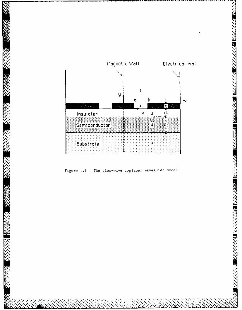
1.1 The slow-wave coplanar waveguide model ................ 4
2.1 Equivalent circuit representation of a slow-wave CPW.. 11
3.1-(a) Propagation constant versus frequency ................. 14
3.1-(b) Real and imaginary parts of the characteristic
impedance versus frequency .......................... 15
3.1 Propagation constant and characteristic impedanceversus frequency obtained by both MMM and SDA ....... 15
3.2 Slow-wave factor and attenuation constand for a CPWmodel ............................................... 17
3.3 Real and imaginary parts of the characteristic
impedance versus frequency for the same CPW withdimensions shown in Figure 3.2 ...................... 18
3.4-(a) 19
3.4-(b) 20
3.4-(c) 21
3.4-(d) 22
4.1 Transient excitation of a slow-wave CPW with thefrequency domain data shown in Figure 3.3 with ashort-circuited input and a capacitive load ......... 25
4.2 Transient pulse waveform with matched source and load
terminations for CPW's with lengths ranging from
I cm to 8 cm ........................................ 27
4.3-(a) Transient pulse excitations with a resistive source
and a capacitive load termination ................... 28
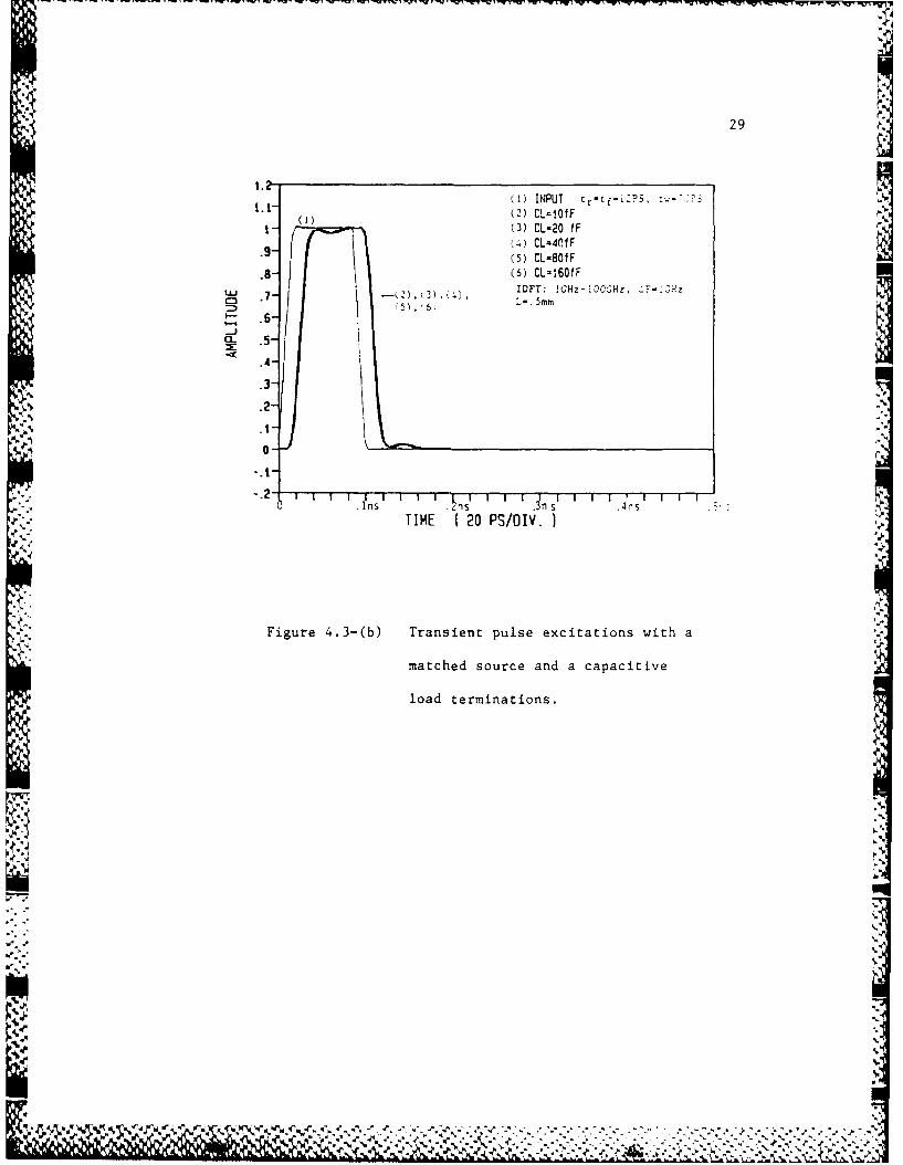
4.3-(b) Transient pulse excitations with a matched source anda capacitive load termination ....................... 29
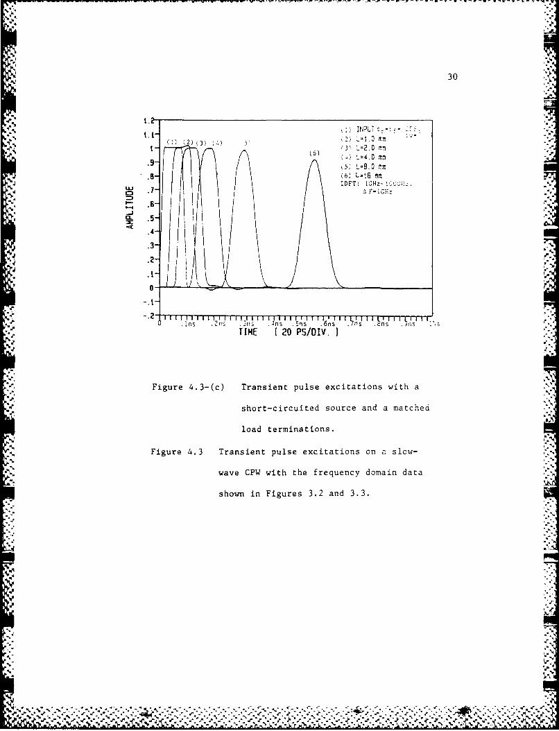
4.3-(c) Transient pulse excitation with a short-circuitedsource and a matched load terminations .............. 30
4.3 Transient pulse excitations on a slow-wave CPW with
the frequency domain data shown in Figures 3.2 and3.3 ................................................. 30
,f. iii
.
' .. . . =,- --.,
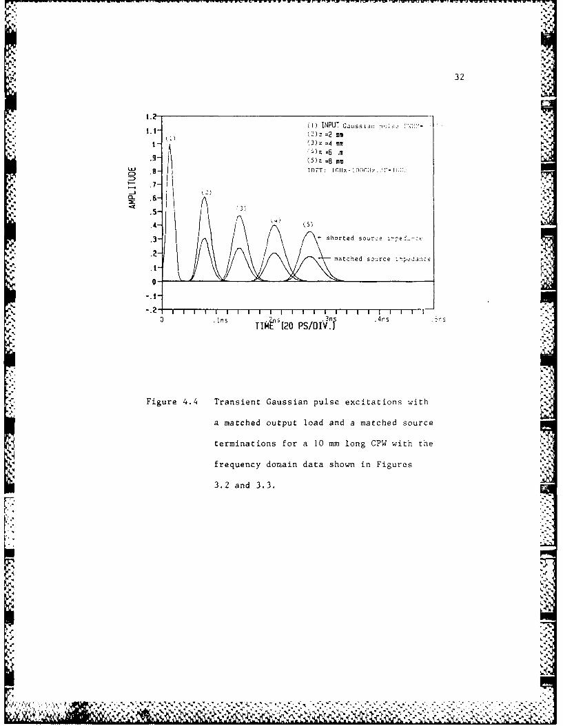
4.4 Transient Gaussian pulse excitations with a matchedoutput load and a matched source terminations for a10 mm long CPW with the frequency domain data shownin Figures 3.2 and 3.3 ............................... 32
4.5 Gaussian pulse transmission along CPW's under matchedterminations with and without semiconducting layer atdifferent locations of the CPW's ..................... 33
I
.4v
s% %
*22"A Il
--- !-- -S
CHAPTER I : Introduction
The advance in monolithic microwave integrated circuits
(MMIC's) and picosecond optoelectronic devices has continuously
improved the switching speed of the active devices and pushed the
real time high-speed signal processing into the picosecond range
[1,2]. Operating at speed higher than gigabits per second, the
conventional lumped capacitance approximation of an
interconnection line in an MMIC can not be used for accurate
analysis on pulse transmission. Instead, microwave considerations
are required in the logic, circuit, and layout of very high-speed
integrated circuits[3]. In addition to the propagation delay, it
is important to know the actual signal waveform after its
propagation along an interconnection line which connects both the
source and the load, since the waveform parameters such as rise
time, fall time, settling time, overshoot and undershoot play a
fundamental role for the success of a very high-speed digital or
wideband analog integrated circuit. The signal degradations
stemming from both the dispersive characteristics of a coplanar
waveguide (CPW) integrated on an MMIC and the improper
terminations will be discussed in this paper.
The CPW has also become an important transmission line
2
element in MMIC technologies because of its easy access for the
ground plane, reduction in crosstalk between adjacent
transmission lines, and less radiation at discontinuities as
compared to a microstrip [4,5]. When a CPW becomes part of a
microcircuit, slow-wave propagation may occur. Planar metal-
insulator-semiconductor (MIS) and Schottky contact CPW were
examined and the existence of the slow-wave propagation was both
experimentally and theoretically confirmed [6.7]. As the physical
dimensions of the CPW are getting smaller, the finite conductor
thickness of a CPW is no longer negligible. Therefore, it is
clear that only accurate field calculations of a CPW can result.
in accurate simulation of an ultra high-speed narrow pulse
transmission on an MIS or Schottky contact slow-wave CPW.
Historical ly, it was reported that severe signal
degradations can occur for pulse transmission along a well
matched semi-infinite lossless microstrip and a CPW for distance
less than 1 cm [8,9,10). The case of pulse transmission with
possible existence of slow-wave propagation was reported in
[11,12,13]. However, no detailed studies have been reported so
far. The purpose of this paper is to present detailed time
domain analyses of pulse transmissions on an MIS or Schottky
contact CPW integrated in a microcircuit under various kinds of ..
input excitationr and arbitrary combinations of source and load
iIr. ]j
,.3
terminations. A hybrid TE and TM full wave analysis based on the
mode-matching method is applied to our model shown in Figure 1.1.
Once the complex propagation constant is obtained, the field
4/.' distributions inside a slow-wave CPW are known. The Poynting
power and the current flowing on the surface of the signal (or
center) conductor of a CPW can be obtained by integrations. This
Nleads to the determination of the complex characteristic
impedance based on the power-current definition. The validity of
the accuracy of the characteristic impedance defined by the
power-current definition is checked against that obtained by the
power-voltage definition based on the spectral domain analysis
(SDA). After the accuracy is confirmed, the inverse discrete
Fourier transform (IDFT) is invoked to convert the frequency
domain data into time domain equivalents. It is found that an
impedance matching scheme can be useful in making a slow-wave CPW
a good interconnection line or a delay line with very little
degradation on the propagating waveform.A,1
.4,..
4J
Magnetic Wal IElectrical Wall
Insulator *X 3
::,,::Semicondutr5a
... ......
. . . . . . . . .
.4% . . . . .
5 u s t r a t e . .... . . . . . . . .
.. . . . .. . . . . .. . . . .
FiueTeslwwv opaa aegiemdl
Z iL6I
CHAPTER 2 : Model and Method of Analysis
A. the Physical Model
The slow-wave CPW model shown in Figure 1.1. was used for
the analysis. The coplanar waveguide with finite conductor
thickness is located on top of a layered structure. It consists
of metal, insulator (or depletion region for Schottky contact),
semiconducting layer (or epitaxial layer), and semi-insulating
substrate. By setting the conductivity of the semiconductor layer
to zero, Figure 1.1 may represent a conventional lossless CPW.
This model is general enough to analyze most CPW's integrated in
MMIC. By knowing the integrated circuit processing data and
physical dimensions , one should be able to compute the time
domain pulse waveform propagating on such a CPW. -e
B. Frequency Domain Analysis
The mode-matching method which has been widely used to
analyze various waveguide structures [14.15) was applied to the w
frequency domain analysis of the slow-wave CPW shown in Figure "
1.1. The technique itself does not result in a unique formulation
for the same problem. Instead, many possible formulations can
5
2 %, C.*
'6
yield the same solution for the propagation constant. Because of
the even symmetry for the propagating mode of interest, a
magnetic wall is placed at the center of the guide. Electric
walls are placed at far distance to simplify the analysis [7].
The modal field expansions in each region shown in Figure 1 can
be expressed in terms of TE-to-y and TM-to-y Hertzian potentials
written as:
A-.
A = e yI(x,y)e -jYz TM-t,,-v
F ey(x,y)e jYz TE-to-y
E . -V x F - jwiioA+ jWEo R
J WE0 Eo
H. A.4 jwEOCRF+ V(V-F)
aER = Er - J W--
(1)
,where Er and a are the relative dielectric constant and the
conductivity of the dielectric material, respectively.
For instance, the potential functions in region 1 are:
%'
-. ~ 4**~.-V~*~'*~
7
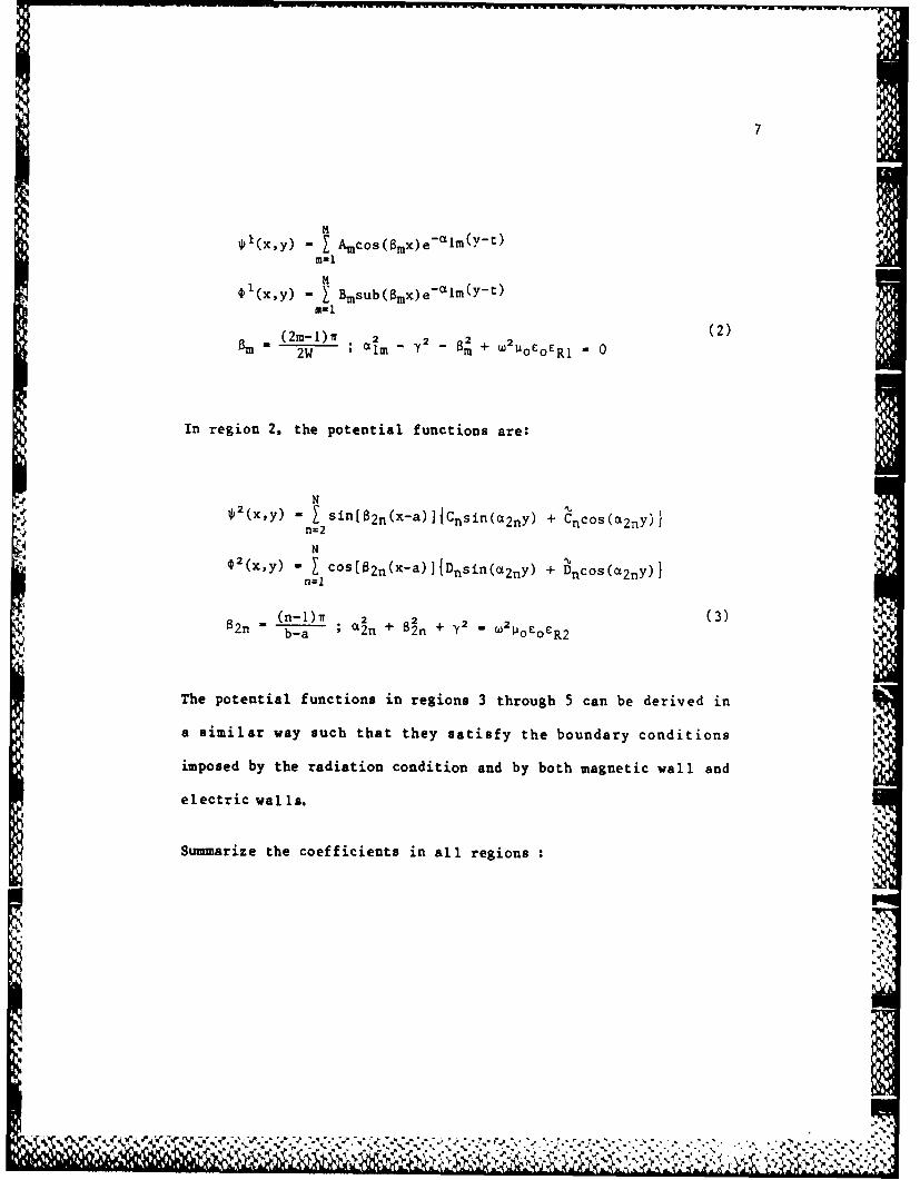
M'P(x,y) - I Amcos(amx)e -a m(Y- t)
m-1
0 (xY) - I Bmsub(Bmx)e-a1m(y-t)M1
(2m-1)r . 2 2(2)am " 2W I a im - - + W oOE6Rl 0
In region 2, the potential functions are:
N,(xy) - I sin[B2n(x-a)]{Cnsin(a2nY) + CnCOS(a2nY)}
n=2
N02 (x,y) - n cos(2n(x-a)]{Dnsin(a2nY) + Dncos(a2nY)}
(n-l__ (3)
2n=(n-1)7r ;,2 + 2+y2.W(3a2n - b-a - 2n + 82n + 9 O " WVICoER2
The potential functions in regions 3 through 5 can be derived in
a similar way such that they satisfy the boundary conditions
imposed by the radiation condition and by both magnetic wall and
electric walls.
Summarize the coefficients in all regions :
.",.. .. .
% e
. , , ,- .,. .,; . .,,£. , - :< -.:,.,.-, , -. , r .. .,,.=.-..:, .. ..>, , ..- ..- ,..
8
Region Coefficients
I Am B
2 CnC n DnD n
3 EmEm FmFm
4 GmGm HmH M(n: '-N)(m:i-M) (4)
By matching the adjacent tangential fields in regions 3
through 5 and applying the orthogonality relationships between
potential functions, only Em and Fm remain. This means that the
coefficients in regions 3 through 5 can be expressed in terms of
Em and Fm only. Next, we match the adjacent tangential fields in
regions 1 through 3. The boundary conditions at the interfaces
of these regions are:
At y=t. Hlt=H2t, 0 < x < b (5)
E1t=E2t* a < x < b (6)
Elt= 0 , 0 1 x I a, b < x I w (7)
At y=O, the boundary conditions are similar to equations (5)
through (7). As the boundary conditions (6) and (7) are satisfied
simultaneously, Am and Bm (Em and Fm) can be expressed in terms
of Cn, Cn, Dn, and Dn. If the boundary condition (5) is
% % %
9
satisfied. Cn. Cn. Dn. and Dn can be expressed in terms of Am and .
Bm (Em and Fm). Finally. a homogeneous matrix equation of
dimension (2N - 1) by 2N -1) can be derived.
C2
Pmn Qmn (Cn........ --. ....-- _- 0 ( AX= 0 )
DlRmn smn
n ,'8
The expressions for Pmn(Y), Qmn(0), Rmn(Y), and Smn(y) are
obtained from the equations (A-1) and (A-2) shown in Appendix. To
obtain a nontrivial solution for the column vector X of the
equation (8). the unknown coefficients of Cn and Dn, the
determinant of the matrix A has to be zero. The real and
imaginary parts of correspond to the slow-wave factor (o/Xg)
and the attenuation constant, respectively.
C. Complex Characteristic Impedance
Once the complex propagation constant Y is obtained, the
unknown field coefficients Cn and Dn are found within a constant
'a2%
oo$
se.#., ;., *,: - .,,' y,..3 .- *" :', . " .". '- , ->*. - "*. .%- . :.7.- . ,. . _v/- " 7 . '- " ." ' ' '",.
10
multiplicative factor. The field distributions in each region are
solved immediately. Based on the power-current definition, the
characteristic impedance is expressed as
5
x Htda 1 'k (Ek, ky-EkVH*X)dakEojt 2 2 I{a da (H I =) .kdzIfi /(H3x)y=o dx + f0 (H2y).8 dY -"
(9)
where the subscript k denotes the subregion k and S is the cross-
sectional area of the CPW.
D. Time Domain Analysis
An equivalent linear 2-port ABCD matrix representation of
the CPW can be applied to derive the complex transfer function
.at a distance of z from the source, of a terminated slow-wave
CPW shown in Figure 2.1 at each incremental frequency step. The
transfer function can be written in terms of Y and Zo as:
VAT.
I
Ml 5
I 't lolo £ '.' . ¢" 2' ,+; '. i ''''..''"''> .-."..'¢ .. .£ .., .-. '-''.i .. -$ ' )
* Z5
90
Figure 2.1 Equivalent circuit representation
of a slow-wave CPW.
% %
12
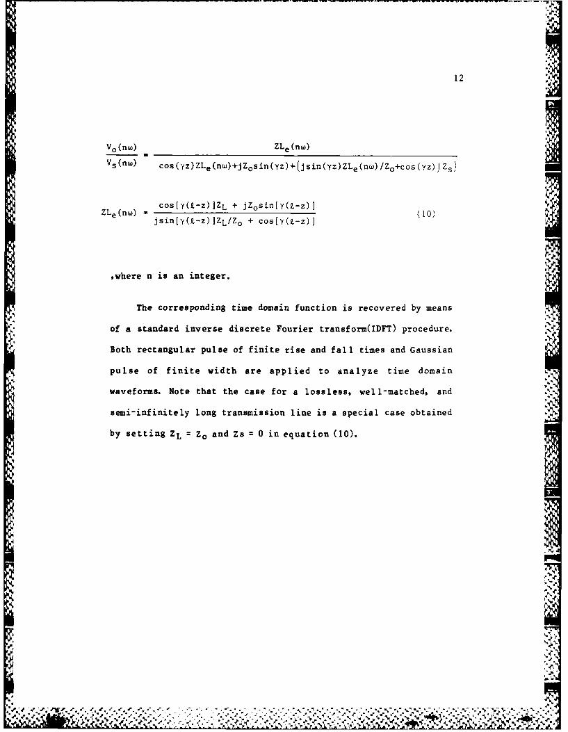
Vo (n) ZLe (nw)
Vs(nw) cos(YZz)ZLe(nw)+JZosin(yz)+(jsin(Yz)ZLe(nw)/Zo+cos(YZ)J Zs)
cos(y(L-z)]ZL + jZosin[y(z-z) lZLe(nw) = jsin[y(t-z)]ZL/Zo + cos[y(Z-z)] (10)
,where n is an integer.
The corresponding time domain function is recovered by means
of a standard inverse discrete Fourier transform(IDFT) procedure.
Both rectangular pulse of finite rise and fall times and Gaussian
pulse of finite width are applied to analyze time domain
waveforms. Note that the case for a lossless, well-matched, and
semi-infinitely long transmission line is a special case obtained
by setting ZL Zo and Zs 0 in equation (10).
S..,S *-S.
' I ,,." -," ".e. .
r~~~ r9'e.
CRAPTER 3 : Frequency-Domain Solutions
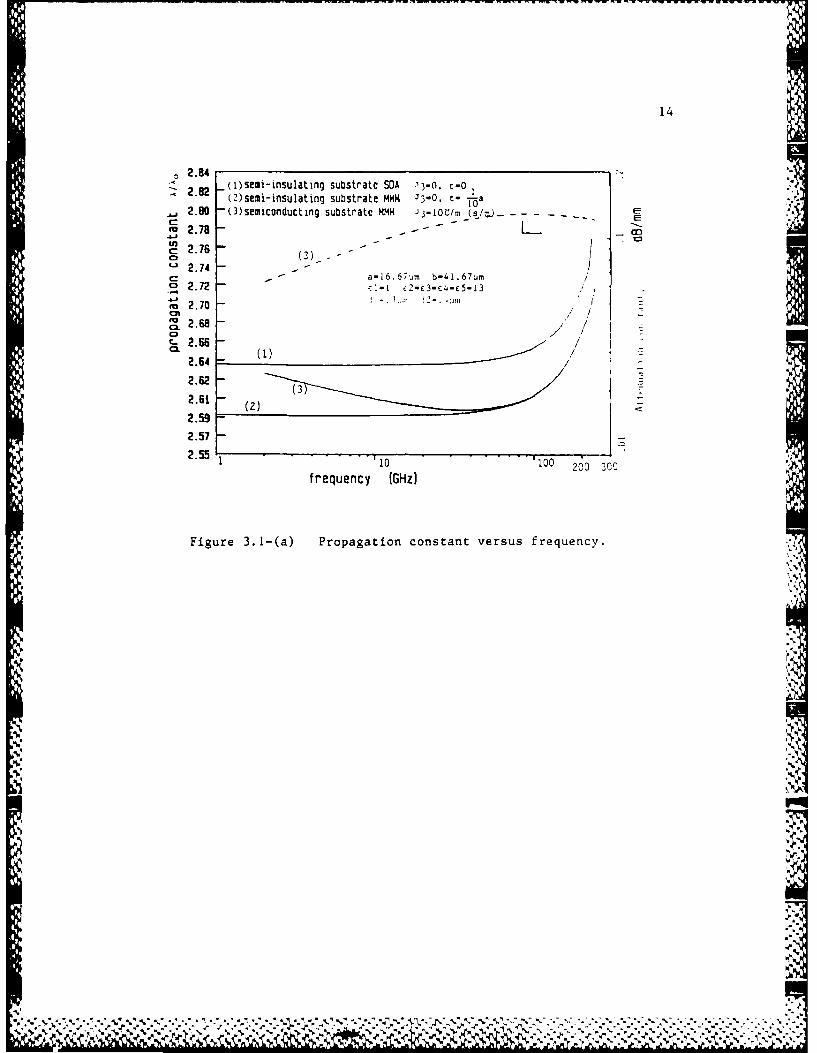
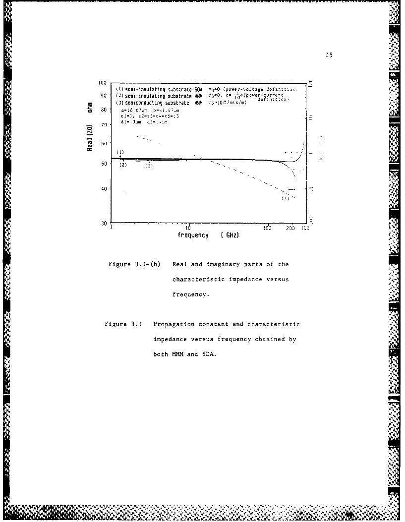
Figures 3.1-(a) and 3.1-(b) are the plots of the
normalized propagation constant and the characteristic impedance
obtained by both MMM and SDA for infinitely thin conductors,
respectively. The discrepancy of the propagation constant shown
in Figure 3.1-(a) between two methods is contributed by the
finite conductor thickness of the CPW analyzed by the MMM. If the
conductor thickness becomes one hundredth of the half center
strip width a, the propagation constants obtained by both MMM and
SDA agree to within .5 Z. It is interesting to see the
discrepancy of the characteristic impedance at higher frequency
among the power-current and the power-voltage definitions
obtained by MMM and SDA. respectively. We may need to incorporate
more basis functions than only two terms currently used in the
SDA code available for our analysis when the CPW under study
starts to depart from the quasi-TEM mode of propagation, since
the quasi-TEM mode approximation is no longer held at higher
frequency and the voltage defined by the integration across the
slot is not a good approximation. In contrast, the current which
can be well defined becomes smaller when the CPW is away from the
quasi-TEM mode. Therefore the characteristic impedance defined by
the power-current definition is higher at higher frequency.
13.-
-0..
14
S2.84(I)semi-insulating substrate SOA :13-0. t-0~ .2 (2)se2i-insulating substrate MMM 1~3-0. t- Toa
2.80 -(3)semicanducting substrate m1Mm Jj-IOU/M (S/M9--------
2.7 -
2.76
S2.74-- -a-16.67,..m b-41.67jm
S2.72 - I-[ Z-E3-E4-c5-13
*~2.70 - I .'I
'CL2.68c- 2.58
2.642.62
2.57
2.510 100 200 300frequency (GHZ)
*Figure 3.1-(a) Propagation constant versus frequency.
%'
'A&
15 -
(1) Sei-lisulating substrate SDA 03- (power-voltage jefin~in90 (2) seii-insulating substrate MMM 03-O0 t- -La(power-currenc
* (3) semicanducting substrate HMM~~msr) eiito
o 30 a-16.67um b- .i.7.I,
cI-1, c2.c3."4s'5.13
70 d1. 3ur d2...-m
60
CC
40-
(3)
3011 100 200 300
frequency (GHZ) t.
Figure 3.1-(b) Real and imaginary parts of the
characteristic impedance versus
frequency.
Figure 3.1 Propagation constant and characteristic
impedance versus frequency obtained by
both MMM and SDA.
V
io, % %% . .'6V
'k %
%
16 -
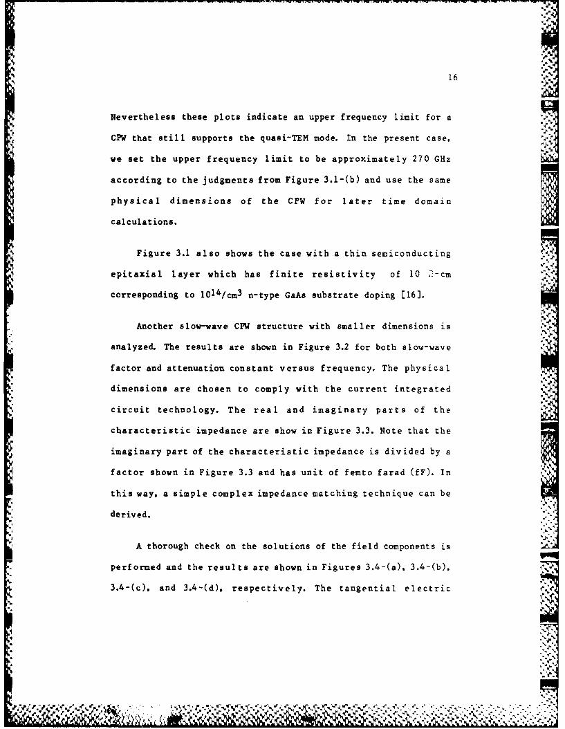
Nevertheless these plots indicate an upper frequency limit for a
CPW that still supports the quasi-TEM mode. In the present case, .1we set the upper frequency limit to be approximately 270 GHz
according to the judgments from Figure 3.1-(b) and use the same
physical dimensions of the CPW for later time domain
calculations.
Figure 3.1 also shows the case with a thin semiconducting
epitaxial layer which has finite resistivity of 10 2-cm
corresponding to 1014/cm3 n-type GaAs substrate doping E6J.
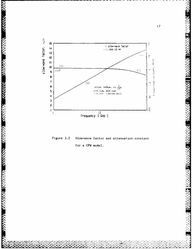
Another slow-wave CPW structure with smaller dimensions is
analyzed. The results are shown in Figure 3.2 for both slow-wave
factor and attenuation constant versus frequency. The physical
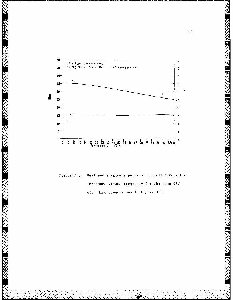
dimensions are chosen to comply with the current integrated .4circuit technology. The real and imaginary parts of the
characteristic impedance are show in Figure 3.3. Note that the
imaginary part of the characteristic impedance is divided by a
factor shown in Figure 3.3 and has unit of femto farad (fF). In
this way, a simple complex impedance matching technique can be
derived.
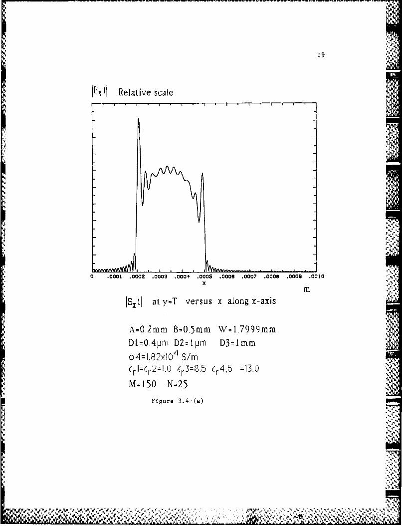
A thorough check on the solutions of the field components is
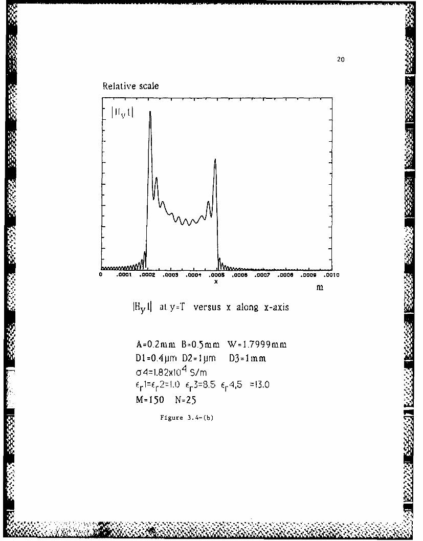
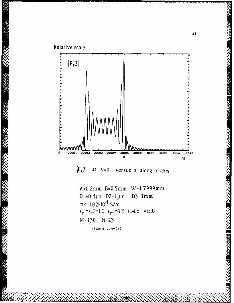
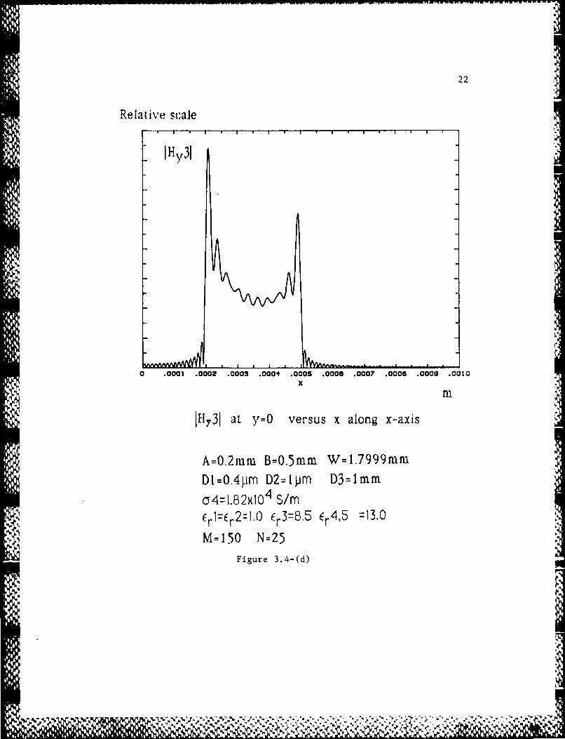
performed and the results are shown in Figures 3.4-(a), 3.4-(b),
3.4-(c), and 3.4-(d), respectively. The tangential electric
p - " , I ,, ',, J " % # d - ". -" -'- . ** . " " . -. -. - .- '."
17
r15 u slow-wave factor
Cj'o- 14 , :,OSS. cS. mm
.4-I
7Li1
d ". 3u2n, d2-.4um1- -1 c=1 i, ' 9;
4
3
2 J
frequency [GHz
Figure 3.2 Slow-wave factor and attenuation constant
for a CPW model.
%b
m 4%
4. "4'
4..
!4•
I A; "- "- ' -"-- ' -4- " ' - '-- - -- -'
'w,4
S()rea I(Z o uni cts: ohm)J
,.45- (2)ImagfZO) i/2 1f/R/R, R= 4.525 OMS (uni ts: fF) 4l
40-0
4' 35335- ---
530-
-30
S 2 5 -2 5
7 2,
' .4
20]
i52
J - -
15
ii
' -o , o t O 5 2 0 i 5 3 0 1 5 4 0 o 4 , '5 - o 5 7' o 7 5 8 o _ 0 6o 1 o0frequen y C (G z)
.q,
Figure 3.3 Real and imaginary parts of the characteristic, -', im pedanc e versus frequen cy fo r the sam e CPW X
Jwith dimensions shown in Figure 3.2.
,
N %]
I ~ I Relative scale
m i... ..
'N ---- -
0 .0001 .0002 .0003 .0001 .0005 .0005 .0007 .0008 .0009 .0010x
In
iEXI at y=T versus x along x-axis
A=0.2umm B=0.5mma W=1.7999rammDI=.4prri D2=lprm D3=ltmmc4=1.82x10 4 S/rn
I.l==( l.o r3=8.5 .4,5 =13.0Er ErIA Er ~ ri 5z3
M=150 N=25
Figure 3.4-(a)
Nk
V .V
" '"? '* ' "; ',*-';.L '.;'",/'g" "''*,'.:'.:.';' ,,-', ',9: "; .. , ; ":" " " ;" .',, "#-.:;.. ,- , ',, , - 5', .': ,,%'" " '' ':"": . , ' -: < .V":"
20
Relative scaleSIIfr,1-
I--.
0 .0001 .0002 .0003 .0004 .000S .0006 .0007 .0008 .0009 .0010
Xrn
IHyII at y=T versus x along x-axis
A=0.2mm B=0.5mum W=1.7999mm
DI=0.4jirr D2= ljm D3=lmm
ao4=1.82x1 04 S/m.,r .l= r2 = . .r3=8 .5 Er4 ,5 = 13.0
M=150 N=25
Figure 3.4-(b)
eA
21
Relative scale
. .I '1 . . . . . .. . . . . ..
0 .0001 .0002 .0003 .0004 .0005 .0005 .0007 .0008 .0009 .oo ox In
IEx3 at y=O versus x along x-axis
A=O.2mm B=O.5mnm W=.7999mm
DI=0.4prm D2=ljpm D3=Imma4:1.82x',04 S/m.r l=.2=. 0 Er3=8 .5 Er4 ,5 =13.0
M=150 N=25Figure 3.4-(c)
-
22
Relative scale
IHpr31
0 .0001 .0002 .0003 .000't .0005 .0006 .0007 .0008 .0009 .00O0
x~m
IH131 at Y=O versus x along x-axis
A=0.2mm B=0.5mm W=1.7999fnm
DI=0.4pim D2=ljm D3=Immc'4=1.82x10 4 S/m
rl=E r2. 0r 3=8 .5 4,5 =13.0
M=150 N=25
Figure 3.4-(d)

* 23
fields and the normal magnetic fields vanish as expected on the
electric conductors with relatively small residues that result
from the MMM employing finite expansion terms. Note also that the
magnitude of the field components shown in these figures has a
peak at the edge of the conductor. In exact field solutions
without numerical approximations. a singularity must exist for
electromagnetic field near the edge of the conductor.
PG
-- 4e
- 4.
)9'"
'4.
4"2V
':": :..:. """" . "":""',":."". "" "-"".":" , "-:;"":?":?"' - i"-4""--..... . : :
CHAPT=R 4 : Time-Domain Results
When a slow-wave CPW is excited by a rectangular pulse of 80
ps rise and fall times (measured by 10-90 percent rise or fall)
and 300 ps wide with zero source impedance and a 10 fF load, a
damped oscillatory output waveform is observed in Figure 4.1.
Figure 4.1 is obtained by means of IDFT that converts the
frequency domain data of Figures 3.2 and 3.3 from .1 GHz to 20
GHz at .IGHz incremental frequency step. When the output load
capacitance(CL) is increased from 10 fF to 80 fF the output
waveform is almost identical. This fact suggests that the output
loading has little effects on the oscillation and the slow-wave
CPW itself has inductive, capacitive and resistive components.
From the circuit point of view, it is not surprising that the
oscillation occurs since there exists a reactive (or positive
imaginary) part of the complex characteristic impedance shown in
Figure 3.3 for the CPW analyzed. As the transient voltage
waveform is excited at the input end of the CPW, the spike wil l
occur just like an inductor will do. Once the input excitation is
settled to a DC voltage, the slow-wave CPW has to reach to the
final steady state in a damped oscillation manner because the
slow-wave propagation of this type usually exhibits a large
capacitance in the low frequency limit [17J and the CPW itself is
24
25
F_ () INPUT Cr Cf 8 OPS c..-3 '?S
1.7 2) RS-CSO0 CL~iOfFIDFT: . IGHz-2OGHz I F-. UHz
t .75-
.5-
.25-
-. I7 T I
ins TIME 2 ?nNS/DIV. 3ns 4ns 5ns
Figure 4.1 Transient excitation of a slow-wave CPW
with the frequency domain data shown in
Figure 3.3 with a short-circuited input
and a capacitive load. 1=1.5 mm
4-
% %!-V
• . ,s
,,-. ." .- -, ,,
%-..4,.% ,'
26
lossy as shown in Figure 3.2.
To make the slow-wave CPW a useful MMIC element it requires
a good wideband matching circuit. It can be demonstrated that if
either source or load impedance is designed to be a complex
conjugate of the complex characteristic impedance (Zo ) of the
CPW, most of the oscillations associated with the transient input
excitation can be suppressed. In this way. a simple parallel RC
network can be applied as a matching network. After a few
algebraic manipulations under the assumption that the imaginary
part of the impedance of the parallel RC network is small, one
obtains X= w R2C, where X and R are the imaginary and real parts
of the complex characteristic impedance, respectively. ( ,is
the angular frequency.) The curve (2) of Figure 3.3 indicates
that the normalized X is almost constant for frequency up to 20
GHz and suggests this is a good choice for C.
Under the matched source and load terminations, Figure 4.2
shows that the rectangular pulse can propagate 8 cm with little
degradation and is delayed by approximately 2.6 ns.
Under the unmatched terminations, the output waveform can
have overshoot or undershoot with some ringing(ripple)
superimposed on top of it as shown in Figure 4.3-(a) [13]. When
the input source impedance is terminated by the matched load
• I4/X.
. . . . . . . . . . . . . . .. . . . . .. . ,_ . T
27
(I)3I INPUT cr-t'-sops 3"
(2) L=4cT3 ) L=2v.i
I ~IDFT: .1GHz-20GH:, <
.7- I
(2) (3) 5)
.4
.3
.2
0 Ins 2ns 3ns 4nszrTIME (A1 NS/DIV.)
Figure 4.2 Transient pulse waveform with matched
source and load terminations for CPW's
with lengths ranging from I cm to 8 cm.
A VA
%S
1tk;
28
1.1) (1 NPUT tr.-cf-12PS, ,-=70PS
(1)(2) RS-iO1(3) RS-20
(3)(4) RS-40(3) RS-80
A- (6) RS-160U- 7 (4) IDFT: IGHz-1OOG~z, AF-IGH:'
* .3-
-
0 Ins .2ns Ani .4 ns tnTIME ( 20 PS/DIV.)
Figure 4.3-(a) Transient pulse excitations w~ith a
resistive source and a capacitive
-, load terminations.
p.N.
29
1.2~1) INPUT tr-tf- 2PS, :'.->2S
t.- (2) CL=!OfF
t (3) CL-20 fF(4) CL-40ffF(5) CL-BOfF
.8 (6) CL--6OfF
W IDFT: !GHz-OOGHz, :F.,,:z
*_ .7- - Z .5mm
--
.4-
.3-
-
A-
.1
-.2 1 1 ins ns s .4n s I ITIME ( 20 PS/DIV. J
Figure 4.3-(b) Transient pulse excitations with a
matched source and a capacitive
load terminations.
%'
,6
C'Va
X ft-M 'r,j .,' ' ", ,K '*. ',,, L' ,"C ,,£' , ,, _ ,; - ., .. .. ... ..., .- , , - - , -. .- - - . ...' ... . . , ., , - - , . .-,
30A
.') INJPUT z-.: .z.
( 2 ) (3) Z.) 2)
(6) (3 =2.0 T.-
k5) L=8.0 I.(6) L=i6 mm$DFT: IGHz- .
S. - F IG Hz
A-
0.. 5-
'a . -
* .2- *f.
Ins .2ns .ns .Ins .5ns 6ns .7ns1 1. i.n s :"sTIME ( 20 PS/DIV.
4.0
Figure 4.3-(c) Transient pulse excitations with a
short-circuited source and a matched
load terminations.
Figure 4.3 Transient pulse excitations on a slow-
wave CPW with the frequency domain data
shown in Figures 3.2 and 3.3.
-4
%,
311
described in the previous section, the output waveform has very
little degradation for driving output capacitive loads up to 160
fF as sbown in Figures 4.3-(b). Figure 4.3-(c) displays the pulse
dispersion for different lengths of the CPW with zero (shorted)
V source impedance and a matched output load. Figure 4.4 shows the
propagation of a Gaussian pulse of 15 ps wide at different
locations of the CPW with a matched output load and either a
shorted or a matched input source termination.
The GaAs MESFET is often fabricated on a thin epitaxialZ.4.
layer with resistivity in the order of 10 Q-cm corresponding to
1014 /cm3 n-type doping concentrations. The results shown in
curves (3) of Figures 3.1-(a) or 3.1-(b) actually correspond to
such a case. These data imply that there exists no slow-wave
- mode or mode transition in the structure under analysis since the N,
imaginary part of the complex characteristic impedance is very
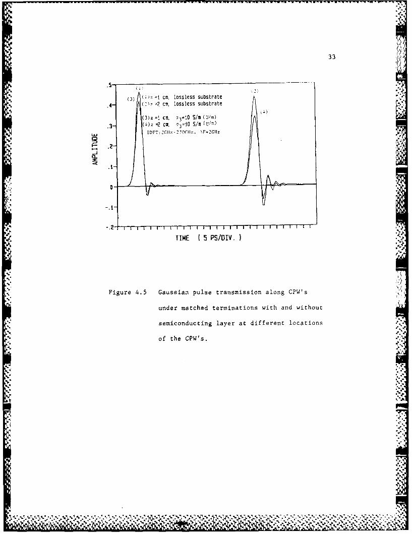
small and is closer to zero at higher frequencies. Figure 4.5,
obtained by converting the frequency domain data shown in Figures
3 .1-(a) and 3.1-(b) into the time domain waveform, compares the
" results of a Gaussian pulse of 5 ps wide observed at I cm and 2
cm from the source end for substrate with and without
semiconducting layer. In this CPW structure, the effect of the
semiconducting layer with small conductivity or low doping
% N .V '
32
." (1) INPUT atLssi,, ,1t .. - (2)z =2 mm
(3)z =4 mm
(5)z =8 mmLL . TTDFT: II 7 - I ,,fl = I .
.6I-- . 7 16.' '
::: .' 3'.5
.4- (5)
.3- shorted source :-'ecn&- c
matched source ipedac
'p 0-
0-,
0'... .n s I'T (20 PS DI . ""
* , %
Figure 4.4 Transient Gaussian pulse excitations with
a matched output load and a matched source
terminations for a 10 mm long CPW with the
frequency domain data shown in Figures :43.2 and 3.3.
'p~'pu
* F *'.*.,4 *%. 4=. 4.
* .- = "A.L~~ %..' * :
33
(3 (1 =t cm, lossless substrate
-2(: - cm. lossless substrate
(3)z =t C,. ;3=, S/M ('3/m)
3- :z -2. 3 2 0 c.I. .\ 2GIIz
" .2
.:1
-A-
-.21-.2- l I , I I I I I l ;
TIME 5 5 PS/DIV.)
Figure 4.5 Gaussian pulse transmission along CPW's
under matched terminations with and without
semiconducting layer at different locations
of the CPW's.
4..4'4..,V

34
concentration attenuates the pulse waveform and does not alter
the shape of the pulse waveform. Similar waveforms are also
reported in [8.9.10) for the cases of a microstrip and a CPW. -
:4 IIIIIN .w
K
CHAPTER 5 : Conclusions
Time domain response of picosecond pulse transmission
along a slow-wave MIS or Schottky contact CPW is presented. The
severe drawbacks such as overshoot, undershoot, and ringing in
applying the slow-wave CPW [12,13] are eliminated almost entirely
by an appropriate wideband impedance matching technique proposed
in this paper. As a result, a slow-wave CPW can be a useful
interconnection line or a delay line in MMIC's. All of these
applications are analyzed separately with examples in the time
domain. We may anticipate other slow-wave structures such as an
MIS microstrip and a coupled microstrip should exhibit similar
properties found in this paper. The theoretical approach
presented in this paper proves to be a versatile tool for the
solutions of very high-speed pulse transmission on an MMIC CPW.
®.
S.
APPENDIX
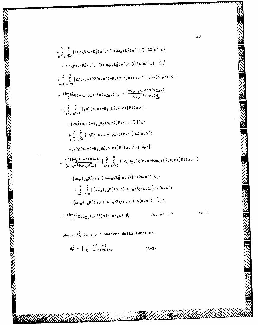
M NI I{R5(m,n)Rl(m,n')+R6(m,n)R3(m,n )}cos(c12--nt)Cn-
mnl n'=2
I I -i~~2t [R5(m,n)RI(t,n')+R6(rn,n)R3(m,n'Mrn1 n'=2 (b-a) W w ~ y
'4 WwO2w-an)
M N
m'=l P-2
+(yRg(m',n') - 62n-Rj(m',n')R3(mp)]Cp
M N
nW -i P=1
+(yRg(m',n') - B2 n-Rg(mn-))R4(mp)IDp}
M N Ii~1nt r[R5(mn)R2(mn)+R6(mn)R4(mn)]
M=1 '= (b-a) W(wy2+EB
M N
E I (wE82nR(m,n')+tjyR5(m',n')R(m',p)m'=lP=2
M N
+ I [(WE.82-R(m,n')+w0 yR(m',n'))R2(m,p)rn'=i P=i 4
+(WF-o2nR(m,n)+oyR(m',n))R4(m',p) ]^D'p
M N
" I I{R5(m,n)R2(m,n2)+R6(m,n)R4(m,n)cos(a 2 n-t) Dn-mn=l n'=1
(b-a) (wui 0y)COS(a2nt)%
4 W(woiy)sin(cz2 nt)Cn + (WU Y2 +WE B2~
m-1 n'=2" (y6g(m,n)82nR8 (m,n)'jR3(mn)]Cn
36
'% %-, IV
37
+ 2ncOs(a2nt) M N R~~)wo~~~)R~~'
+(wco8 2nRg(m,n)+wu0yRi(m,n))R3(m,n')]Cn-
M N+ Z [(WE0B2nR (m,n)+wiiyRj(m,n))R2(m,n')
mJl n'=l
+(w0 o2 ,Rg(m,n)+ww0 yRgm,n))R4(m,n )IDnI
(b-a) frn- Ai4 WCa2na2n)sifl(a2nt) Dn o :- A1
M NI I{R7(m,n)RI(m,n')+R8(m,n)R3(m,n2 }cos(ct2n-t)Cl-
m1l n'-2
MNsifl(c2n't) _ [R7(m,n)RI(m,n')+R8(m,n)R3(m,n')]
mzl n'=2 (-a4)W( wly 2,
M N
+(yRg(m,n') - 62n-R(,n'))R3(m,p) ICp
+ I [(yR(m,n') - S2n-R(m,n))R2(m',p)-'~ PM1
+(y~~m'n')- B2nlRj(m',n'))R4(m',p)] pl
M s in(a2n-t) _(R7(m,n)R2(m,n')+R8(m,n)R4(m,n')Imlns1 -,, 4 2O+WCJOB2 )
M N
Y [(WEo2nRm,n)+wwoyR(m',n))Rum',p)m =1 P=2
+(~BnR~'n)wjyim,')3m,)C
-. % . 4
38
+ ((WE 06 2nR (m,n')+wpoyR(mn))R2(mP)m'=1 P=1
+(wCo 2nR;(n')+woyRj(m',n-))R4(m',p)] DPI
+ I I R7(m,n)R2(m,f)+R8(m,n)R4(m,n)cos(2nt)Cnm=1 n'=1
'b) (wio62n)cOs (a2nt)
m NI [(yR(m,n)-B2nRj(msn))R1(mn)
m=1 n'=2
+(~yR [4y)6R(mp8nR3(msn')]R(Cn)
+ (yRnn) 2 (m,n))~R(m~n))2(mn'
=1 n'1 .
Y(+6l)o(~2n- _I I I (WEoB2nR;(m,n)+wuoyRim~n))R1(m~n')TW7 WO ) m=1 nO=2
a
+rw~a~R~m wpR8 (m,n))R3(m,n')]n
+ 1 (weoa2nR5(m,fl)+wIpoyR(,n))R2(m~n')m=1 n'=1
+(WcoB~nR (m,n)+wpyRg(m,f))R4(m~n')] Dn'
+(-a)w DyL L6)sf~~) for n: P-N (A~-2)
where 6. is the Kronecker delta function,
I 1 if n-i6nl 0 otherwise (A- 3)
-,% %
39
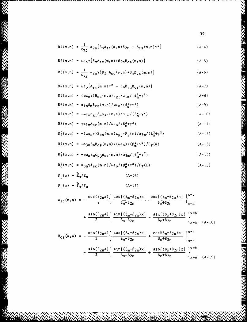
R1(m~n n 1 02n(6mAsc(m,n)S2n - Bcs(m,n)y2 (-4
R2(m,n) -WEoY(BmAsc(m,n)+B2nBcs(m,n)) (A-5)
R3(m~n) I 2nY(62nAsc(m,n)+8mBcs(m,n))(A6CR2
R4(m,n) -weo(Asc(m,n) y2 - Bm82nBcs(m,n)) (A-7)
R5(m,n) - (wL±0y)Bcs(m,n) ERI /aM/(Bl+y2 ) (A-8)
R6(m,n) - aImBmBcs(m,n)/WEo/ (82+y 2 ) (A-.9)
R8(m,n) - yimAsc(m,n)/WE o/(B2+y2) (-i
Rj(m,n) - -(wuoy)Bcs(m,n)ER3*PE(m)/a3m/(8'+y2) (A-12)
Rg(m,n) - -c3m~mBcs(m,n)/(WEo) /(86i+y 2 )/pF) (A-13)
Rj(m,n) - -wIo8msR3ASC(mjn)/c13m/(y) (Am
Rj(rn,n) - a3myAsc(m,n)/eo/ (B2+y 2)/pF) (A-15)
PE(m) -hi/Em (A-i16)
PF(m) = am/Fm (A-17)
A 'mp) =cos (62ra){ +OIB-6n COS(am+B2n)x] x=b
2C - -62n Bm+B2n x~a
sin($2na)f sifl(Bm 62n)x] sifl[(Bm+B2n)x] ~+ 2 ~ Bm-2n Bm+B2n Ka (A-18)
}x=bBcs(mvfl) - 2 " -ma~ B 0m+B2n )x a
sin(B2na){ sin[(8m-2n)x] sifl[(Bm+a2n)x] x=b p
Bm-62n + 8 2n x=a (A-19)
% k '64%
I "q.% %'
N %
References
[] C.P. Lee, P.L. Miller, D. Hou, and R.J. Anderson,'Ultra high
spped integrated circuits using GaAs/GaAIAs high mobility
transistors,'in Proc. Device Research Conf. IIA-7, June
1983.
[2) R.K. Jain, K. Stenersen, D.E. Snyder,'Picosecond
optoelectronics in high-speed integrated circuits',
Proceedings of SPIE, Vol. 439. pp. 174-176, 1983.
[3) H. Hasegawa, S. Seki,'Analysis of interconnection delay on
very high-speed LSI/VLSI chips using an microstrip line
model,'IEEE Trans. Microwave Theory and Tech., vol. MTT-32.
no. 12, pp. 1721-1727, Dec. 1984.
[4) M. Riaziatl. ZubeckS. Bandy, and G. Zdasiuk.'Coplanar
waveguides used in 2-18 GHz distributed amplifiert'IEEE MTT-
S International Microwave Symposium, pp. 337-338, June
1986.
[5] R.W. Jackson, 'Coplanar Waveguide vs. microstrip for
millimeter wave integrated circuits,'IEEE MTT-S
International Microwave Symposium , pp. 699-702, June 1986.
[6] H. Hasegawa and H. Okizaki,'M.I.S. and Schottky slow-wave
coplanar stripline on GaAs substrate,'Electron. Lett., vol.
13, pp.6 6 3-6 6 4 , Oct. 1977.
40
S%,,'
{. * * . .. - - - .~* *'* '' ~*A*
41
[7] Y. Fukuoka. Y. C. Shih, and T. Itoh,'Analysis of slow-wave
coplanar vaveguide for monolithic integrated circuits,'IEEE
Trans. Microwave Theory Tech., vol. MTT-31, no.7, pp. 5 67 -
573. July 1983.
[8) K. K. Li. G. Arjavalingam, A. Dienes, and J. R.
Wbinnery'Propagat ion of picosecond pulses on microwave
striplines,'IEEE Trans. Microwave Theory and Tech., vol.
MTT-30, no. 8. pp.1270-i 2 7 3 , August 1982. 4[9) G. Haanain, A. Dienes. and J. R. Whinnery,'Dispersion of
picosecond pulses in coplanar transmission lines,'IEEE
Trans. Microwave Theory and Tech.. vol. MTT-34, no. 6, pp.
738-741. June 1986.
[10] R. L. Veghte and C. A. BalanisDispersion of transient
signals in microstrip transmission lines,'IEEE MTT-S
International Microwave Symposium digest. pp. 691-694. June
1986.
[11) C.Seguinot, P.Kennis, P.Pribetich, J.F.Legier,'Crosstalk
phenomenon in coupled microstrip lines laid on semi-
conducting subs trates,'l 5th European Microwave Conference
Digest. pp. 826-830, Paris, Sep. 1985.
[12] C-K Tzuang and T. Itoh,'Pulse transmission on a slow-wave
MIS and Schottky coplanar waveguide with finite conductor
thickness.115th European Microwave Conference Digest , pp. a
V~~~~~. .i .NI NX1
U a'
42
225-230, Paris, France, Sep. 1985.
[13] C-K Tzuang and T. Itoh,'Pulse transmission in an
interconnection line on a semiconductor substrate with a
lossy layer,'1985 VLSI Multilevel Interconnection
Conference Digest, pp.424-430 June 25-26, Santa Clara. CA.
[14) R. Mittra, Y. L. Hou. and V. Jamnejad.'Analysis of open
dielectric waveguides using mode-matching technique and
variational methods.'IEEE Trans. Microwave Theory and Tech..
vol. MTT-28, pp. 36-43, Jan. 1980.
£15) G. Kowalski and R. Pregla,'Dispersion characteristics of
shielded microstrips with finite thickness,'Arch. Elek.
Ubertragung, vol. 25, no. 4, pp.193-196, April 1971.
[16) Sze,'Physics of Semiconductor Devices,'pp.33, 2nd edition,
1981, John Wiley & Sons, Inc.
[17) H. Ogawa and T. Itoh,'Slow-wave characteristics of
ferromagnetic semiconductor microstrip lines,'IEEE MTT-S
International Microwave Symposium Digestpp.65-68, June
1986.
'IIr
.
y r
T '1 I~b
4;