Embed Size (px)
Citation preview

UNCLASSIFIED
AD NUMBER
LIMITATION CHANGESTO:
FROM:
AUTHORITY
THIS PAGE IS UNCLASSIFIED
AD868121
Approved for public release; distribution isunlimited.
Distribution authorized to U.S. Gov't. agenciesand their contractors; Critical Technology; AUG1968. Other requests shall be referred to AirForce Weapons Laboratory, ATTN: WLRET, KirtlandAFB, NM 87117. This document contains export-controlled technical data.
AFWL ltr dtd 30 Nov 1971

•»*•' •amwi •eft.
1
AFWL-TR-68-31, Vol I
a WWL-TR
Voll
A
>£> A
5
RADIATION EFFECTS ON GALLIUM ARSENIDE
DEVICES AND SCHOTTKY DIODES
J /
/
Volume I
R. H. Schnurr
H. D. Southward
LOAN COPY: RETURN TO AFWL (WUL-2)
KIRTLANO AFB, N MEX
University of New Mexico
Albuquerque, New Mexico
Contract F29601-67-C-0051
TECHNICAL REPORT NO. AFWLTR-68-31, Vol I
August 1968
^
AIR FORCE WEAPONS LABORATORY
Air Force Systems Command Kirtiand Air Fore« Base
N«w Mtxico "••>
• Thla document ia subject to apeclal export control« and each traneailttal to foreign government» or foreign nationale hay be made only with prior sppro¥*l of AFWL (WLRET) , Kirtiand AFB, Mt, 8/117
Reproduced by the CLEARINGHOUSE
for Federal Scientific & Technical Information Springfield Va. 22151
•ml»*—
u

-—
AFWL-TR-6&-31, Vol I
AIR FORCE WEAPONS LABORATORY Air Force Systems Command Kirtland Air Force Base
New Mexico
When U. S. Government drawings, specifications, or other data are used for any purpose other than a definitely related Government procurement operation, the Government thereby incurs no responsibility nor any obligation whatsoever, and the fact that the Government may have formulated, furnished, or in any way supplied the said drawings, specifications, or other data, is not to be regarded by imp? cation or otherwise, as in any manner licensing the holder or any other person or corporation, or conveying any rights or permission to manufacture, us<3, or sell any patented invention that may in any way be related thereto.
This report is made available for study with the understanding that proprietary interests in and relating thereto will not be impaired. In case of apparent conflict or any other questions between the Government's rights and those of others, notify the Judge Advocate, Air Force Systems Command, Andrews Air Force Base, Washir oon, D. C. 20331.
DO NOT RETURN THIS COPY. RETAIN OR DESTROY

AJWL-TR-68-31, Vol I
RADIATION EFFECTS ON GALLIUM ARSENIDE DEVICES AND SCKOTTKY DIODES
Volume I
R. H. Schnurr H. D. Southward University of New Mexico Albuquerque, New Mexico
Contract F29601-67-C-0051
TECHNICAL REPORT NO. AFWL-TR-68-31
This document is subject to special export controls and each transmittal to foreign governments or foreign nationals may be made only with prior approval of AFWL(WLRET), Kirtland AFB, NMex 17117. Distribution is limited because of the technology discussed in the report.

—m
AFWL-TR-68-31, Vol I
FOREWORD
This report was prepared by the university of New Mexico, Albuquerque, New Mexico under Contract F29601-67-C-0051. The research was performed undex Program Element 6.16.46.01H, Project 5710, Subtask 6.015, and was funded by the i^fense Atomic Support Agency (DASA).
Inclusive dates of research were 15 February 1967 to 15 February 1968. The report was submitted 7 June 1968 by the AFWL Project Officer, Dr. J. S. Nichols (WLRE). Former Project Officers were Capt John Hubbard and Capt Gary Pritchard (WLRE).
The authors wish to express their sincere appreciation to Texas Instruments, Inc., for aid and cooperation in the pursuit of this research contract. We would like to specifically acknowledge the cooperation of Gary Hanson who coordinated our visits, of Hans Strack for helpful discussions involving GaAs, and of Shing Mao for helpful discussions involving the Gunn diodes.
The authors wish to acknowledge the assistance of MSgt Fred W. Fisher,. SSgt Albert H. Hoifland, and SSgt Jon S. Toops for their operation of the flash X-ray machine.
This technical report has been reviewed and is approved.
S. NICHOLS »roject Officer
WILLIAM N. JACKOMIS Major, USAF Chief» Effects Branch
#
«4 *** *v CLAUDE K. STAMBAUGH Colonel, USAF Chief, Research Division
ii

i» ,ji in •mifiiiii ill r» ij—iwr'nimiiini
AFWL-TR-68-31, Vol I
ABSTRACT
(Distribution Limitation Statement No. 2)
The theory of operation of the Schottky barrier diode is reviewed, and complica-
tions caused by a more accurate space-charge formulation are discussed. Con-
sideration is given to image effects, tunneling, interfacial dielectric layers,
surface states, and minority carrier current.
The interaction of ionizing radiation with semicond' cing materials is reviewed,
as is the behavior of a Schottky barrier diode in an Ionising radiation environ-
ment. The resultant model for the Schottky barrier diode is analogous to a
p-n diode with a very high dopant concentration on one side.
Tests were performed upon gallium arsenide (GaAs) and silicon Schottky barrier
diodes, using a 2-Mev flash X-ray machine. The GaAs Schottky diodes were
tested while functioning as an X-band detector and mixer. Mo permanent change
was observed in the voltage-current or capacitance-voltage characteristics, or
in the noise figure of the diodes after irradiation. Diodes fabricated from
both types of material were also tested in a more conventional DC bias circuit.
Both types of diode were exposed to a mixed neutron gamma pulse at the Sandia 14 Pulsed Reactor II. Neutron fluency up to 5 x 10 nvt and gamma dose rates up
9 to 10 rad/sec were obtained. The diodes showed very minor changes in voltage
current characteristics for a total neutron fluence up to 1.2 x 10 nvt.
ill

-
AFWL-TR-68-31, Vol I
This page intentionally left blank.
iv

CONTENTS
SECTION PAGE
I. INTRODUCTION 1
II. SCHOTTKY BARRIER THEORY 4
Elementary Schottky Barrier Theory 4
The Effect of a More Accurate Space Charge Formulation 15
The Effect of Image Force on Barrier Shape 19
The Effect of Tunneling 21
'.'he Effect of Interfacial Layers 22
The Effect of Surface States 29
The Effect of Minority Carrier Current 43
III. RADIATION EFFECTS ON SCHOTTKY BARRIER DIODES 44
IV.
Interaction of Ionizing Radiation with Matter
Effect of Ionizing Radiation upon Semi- conductors
Effect of Ionizing Radiation upon Schottky Barrier Diodes
EXPERIMENTAL RESULTS
Diode Characteristics
Results of Tests Using Flash X-ray Machine
APPENDIX I:
APPENDIX II:
APPENDIX III
REFERENCES
BIBLIOGRAPHY
DISTRIBUTION
DERIVATION OF VELOCITY DISTRIBUTION OF ELECTRONS FROM FERMI-DIRAC DISTRIBUTION
EXPERIMENTAL FACILITIES AND EQUIPMENT
RESULTS OF NEUTRON TESTING OF SCHOTTKY BARRIER DIODES
44
47
73
89
95
98
103
106
108
*' mu '

LIST OF FIGURES
Figure
1 Metal Semiconductor Junctions
2 Metal Semiconductor Junction with Applied Reverse-Bias Voltage V
3 Distortion of the Barrier Caused by Image Effects
Page
5
7
8
9
10
11
12
13
14
15
16
17
Metal-Insulator-Semiconductor Junction
Free Semiconductor Surface with Surface States
Metal-Insulator-Semiconductor Junction with Surface States
Energy Bands as a Function of Lattice Spacing
Metal-Insulator-Semiconductor Junction with qVDO < Eg '1 »2 -»n Metal-Insulator-Semiconductor Junction with
«"DO a Eg - H - »2 " %
Schottky Barrier During and Immediately After Ionizing Radiation Pulse
Charge Accumulation in the Oxide Passivation
Schottky Barrier Diode Geometries
Capacitance versus Voltage for TIXV19 and TIV305 Diodes
1/C versus V for a TIXV19 Schottky Barrier Die^e
1/CZ versus V for a TIV305 Schottky Barrier Diode
Construction Profile of a Typical Schottky Barrier Diode
Current versus Voltage for a TIXV19 Schottky Barrier Diode
21
24
30
33
37
39
40
55
57
59
61
62
63
64
68
vi

List of Figures (continued)
Figure
22 Response of Silicon Schottky Bprrier Diode to X-ray Pulse
18 Current versus Voltage for a TIV305 Schottky Barrier Diode 69
19 Conventional Diode Test Circuit 74
20 Response of GaAs Schottky Barrier Diode in Waveguide to X-ray Pulse 76
21 Response of GaAs Schottky Barrier Diode to X-ray Pulse 77
78
25 Circuit for Testing GaAs Schottky Barrier Diode as an X-band Detector Diode 81
24 Peak Photocurrent versus Bias Current for TIXV19 Detector Diode 82
25 Circuit for Testing GaAs Schottky Barrier Diode as an X-band Mixer Diode 84
26 Response of GaAs Schottky Barrier Diode Operating as a Mixer Diode to an X-ray Pulse as Seen at the Output of the I-F Amplifier 86
27 Maximum Peak to Peak Voltage versus Bias Current for TIXV19 X-band Mixer Diode 87
28 Typical Test Configuration Showing Screen Room and Flash X-ray Machine 96
29 TIXV19-7 V-I Characteristics Before and After Exposure to Neutrons 100
30 TIV305-5 V'1 Characteristics Before and After Exposure to Neutrons 102
«a
vii

'
A
C
Dn
EB
E
E.
E.
EiB
E io
in
E mo
v
Ex
Ln
LIST OF SYMBOLS
2 area of diode junction, meters
capacitance of diode junctions, farads
2 diffusion constant for electrons, meters /second
2 diffusion constant f r holes, meters /second
electric field, volts/meter
energy on top of potential barrier, electron volts
energy of conduction band, electron volts
energy of Fermi level, electron volts
width of forbidden band gap, electron volts
energy of center of forbidden band gap, electron volts
energy of center of forbidden band gap in bulk
material, electron volts
electric field across insulator, volts/meter
maximum electric field, volts/meter
maximum electric field with zero applied bias, volts/
meter
energy necessary to produce one electron-hole pair
by radiation, electron volts
energy of valence ijand, electron volts
energy associated with particle of velocity v ,
electron volts
diffusion length for electron,meters
diffusion length for holes, meters
acceptor density, meter -3
ND donor density, meters J
viil

Ns
ss
R
T
V
V BO
V D
V DO
vi Vio
9
j
u j_
jo
k
I
'a m*
List of Symbols (cont'd)
surface state density, [electron volts -mete xL 3""*
charge in metal. Coulombs
charge in space charge region. Coulombs
charge in surface states, Coulombs
dose rate, rads/second
temperature, °K
applied bias voltage, volts
barrier height caused by surface states, volts
barrier height, volts
barrier height with zero applied bias, volts
voltage across insulator, volts
voltage across insulator with zero applied bias, volts
electron-hole pair generation rate, meters"^
net current density, amperes/meter o
positive current density, amperes/meter
negative current density, amperes/meter o
electon current density, amperes/meter
reverse saturation current density, amperes/meter^
2 hole current density, amperes/meter
component of current density in x direction, amperes/ 2 meter
Boltzmann constant, 1.38 x 10" * joules/°K
depletion width, meters
depletion width with zero applied bias, meters
effective mass, kilograms
ix
; •-—

'•"••• "•••' T* -'" •""•"•«•'
_-,_,,„.-.-
.,., I..,,..-. -.--.—» >. . -J
n
ni no
nx
p
'x
w
X
XB
«i
*P
P
p(x)
List of Symbols (cont'd)
,-3 electron concentration, meters
electron concentration for intrinsic material, meters"-^
thermal equilibrium density of electrons in the con-
duction band, meters -3
rP 9 m
density of mobile electrons in conduction band with
a velocity in the x direction, meters *
hole concentration, meters"^
electronic charge, 1.6 x 10" * Coulombs
x component of velocity, meters/second
width of insulator, meters
distance into semiconductor measured from surface,
meters
location of potential barrier maximum, meters
dielectric constant of insulator, farads/meter
dielectric constant of semiconductor, farads/meter
electron mobility, meters/volt-second
hole mobility, meters/volt-second
density of material, kilograms/meteir
volume charge density, Coulombs/meter
minority carrier lifetime for electrons, seconds
minority carrier lifetime for holes, seconds
work function of metal, electron volts
work function of semiconductor, electron volts
electron affinity for insulator, electron volts
electron affinity for semiconductor, electron volts

List of Symbols (cont'd)
i/) potential distribution, voxts
A0 change in maximum potential, volts
^sc potential distribution in semiconductor, volts
#„ potential distribution in semiconductor with zero SCO r
applied bias, volts
V
\
xi

-""—•• - • IL -
AFWL-TR-68-31, Vol I
/
This page intentioually left blank.
xii

IllIIII •
SECTION I
INTRODUCTION
'
Metal semiconductor junctions have been studied for
many years (Ref. 1). The point-contact rectifier has been
used since the earliest days of radio. The most satisfactory
early rectifiers, based upon lead sulphide, could not be
reproduced with precise uniformity. Other rectifiers were
made from germanium and silicon pellets which were ground
smooth and polished. The junction was formed by touching
the semiconductor with a thin metal wire. The wire tip was
moved until a sensitive spot was found. Mechanical tapping
of the whisker mount improved the rectification and stability
of the device. Mechanical forming of point-contact diodes
is still used.
The development of a workable theory for the metal
semiconductor junction had to wait for the development of
the band theory of solids. Theories explaining the behavior
of the metal semiconductor junctions were formulated by
Schottky and Mott. These models are the basis for the more
elaborate theories of today. As technology was able to
provide more uniformly reproducible rectifiers, the first
theories have been modified and refined to explain addi-
tional experimental data.
•

»"' "" '••""" ' '. » •'"' II •••
Modern technology is now able to form deposited metal
contacts the same size as the point of the wire in the
point-contact diodes. This capability is reflected by
the appearance of metal semiconductor or Schottky barrier
diodes on the commercial market. The Schottky barrier
diodes are stronger mechanically than point-contact diodes.
The junction of the Schottky barrier diodes is formed under
controlled conditions and is therefore more precisely
reproducible.
Schottky barrier diodes are used as parametric ampli-
fiers, harmonic generators, multipliers, mixers, high-speed
switches, and voltage-tuned or modulated oscillators.
Because of their versatility, Schottky barrier diodes can
be used in many sophisticated military and space systems.
Military and space systems may be exposed to environ-
ments containing high radiation levels. Consequently,
the circuit designer must know the el*feet of radiation
upon the components he uses in order to minimize undesirable
radiation-induced transients or changes in the system.
Information is available which describes in detail
the effect of radiation upon pr-n junction diodes, tran-
sistors, integrated circuits, and other active and passive
components. This paper has been written to characterize
the Schottky barrier diode in a radiation environment.
The simple theory of a metal semiconductor junc-
tion as proposed by Schottky is developed in the
first part of Section II. A more accurate formula-
tion for the space charge is discussed. Considera-
tions of image effects/ tunneling, interfacial dielectric
layers, surface states, and minority carrier current are
also included.
Section III begins with a discussion of the inter-
action of ionizing radiation with matter. The interaction
processes discussed are photoelectric, Compton, pair
production and photodisintegration. The effect of ionizing
radiation upon semiconductors is then considered. Section III
is concluded with a discussion of the effect of ionizing
radiation on Schottky barrier diodes.
The Schottky barrier diodes were irradiated at the
Kirtland Air Force Base 2-Mev flash X-ray machine. The
results of these tests are reported in Section IV. The
photocurrent was measured and compared with the theory
developed in Section III. The diodes were also tested
operationally as detectors and mixers.
Purther testing is reported on in Appendix III. The
Schottky barrier diodes were irradiated at the Sandia
Pulsed Reactor II. Transient annealing and permanent
degradation of the diodes were observed.

I*lr~^l»wi«
SECTION II
SCHOTTKY BAPRISR THEORY
To provide an insight into the theory of a Schottky
barrier, the simple model proposed by Schottky is dis-
cussed. Next, complications are considered that arise
from more nearly exact space configurations, image
force, quantirr.-mechanical tunneling, surface states,
interfacial dielectric layers, and minority carrier
currents -
Elementary Schottky Barrier Theory
The simplest model for the rectifying metal semi-
conductor junction is that developed by Schottky. The
model is best explained by use ox the band model of solids
showing the band structure in the metal and semiconductor
both before and after contact.
In figure la, a metal semiconductor junction is shown
before contact. <pm is the work function of the metal, q>, m s
is the work function of the semiconductor, and xo is called s
the electron affinity of the semiconductor. There is an
energy difference of 9 - <p between the Fermi levels in HI D
the metal and those in the semiconductor.
When the two materials are brought into intimate
contact, thermal equilibrium requires that their Fermi
levels coincide. It may be reasonably assumed that both
materials were originally uncharged and that both materials

—-•
* m
'*m7, VACUUM
METAL
n x *
SEMICONDUCTOR
a) Before contact
V/////////7Z b) After contact eid with thermal equilibrium
Figure 1. Metal Semiconductor Junction
5

will exhibit their bulk properties at some distance from
their common interface. The contact potential, caused by
the difference in Fermi-level energies, must, therefore,
appear across the junction. The contr.ct potential, de-
fined by
VD0 " q 'vm " *s' ' (1)
will cause a redistribution of charge at the junction.
Schottky proposed that a double layer be formed at ,
the junction. At the instant a junction is established,
electrons will flow from the semiconductor into the metal
until the contact potential is neutralized by the charge
layer. A negative surface charge is developed upon the
metal. An opposite and equal charge must be built up in
the semiconductor, but in the absence of surface states
the positive charge must be distributed over fixed ionized
atoms in the semiconductor forming a space charge layer.
The resultant charge distribution after contact is illus-
trated in figure lb.
The customary treatment of the problem is to assume
a uniformly doped semiconductor with the impurity donor
density, N_.. Further, assume the semiconductor is com-
pletely depleted of electrons for a distance, i , from
the junction. The depletion width, i , can be determined
by solving Poisson's equation
—
d2* m _ p(x)
dx" cs (2
where
t& = potential distribution
x • distance into semiconductor from the surface
p(x) = space charge density
t = dielectric constant of the semiconductor 8
Prom the assumptions we can write,
p = + q ND 0 i x <: i
p = 0 iQ < x
The boundary conditions for equation 2
o
*Ä*i 1/2
x = £ , and ij; = 0 at x = Än. o o
t-f L-3C
are
(5)
0 at
W
'SCO
qN
2* 1 rx - -y2
s 0 * x <. i (5)
and
mo gtfJBf] V2 2V. DO (6>
*
We define »A as the potential distribution in the semi- vBCO
conductor with no bias applied and E_ as the maximum r,r mo
electric field with no bias applied.
1 ••••

Behavior with Applied Bias
The effect of applied bias is easily incorporated
into equations 4, 5# a«*d 6. Suppose a bias voltage is
applied in some manner to a Schottky barrier device so
that the n-type semiconductor is made positive with respect
to the metal. The total applied voltage must be shared
by voltage drops across the ohmic contacts, the bulk mate-
rial, and the barrier region. For small currents»the
"oltage drops across the ohmic contacts, and bulk material
can be neglooted. The voltage drop across the barrier
region will cause a change in the barrier as illustrated
in figure 2. Equations 4, 5# and 6 can be generalised to
give the variations in depletion width, potential, and
electfic field with an apslded bias:
L qff D •] qN D
5
m = r2qt,p(vDo + v)i1/2 2(vD0 + VI
(T)
(8)
(9)

VS s/////// /
Figure 2. Metal Semiconductor Junction with Applied
Reverse-Bias Voltage V
Junction Capacitance
A charge, Q__# is stored in the depletion region.
Its magnitude is dependent upon the volume charge density,
0{x), and the width of the depletion region. That is,
Qsc = P M i
<*D* = [2«sNDq(VDO +V)J1/2 10)
The total charge is dependent upon applied voltage. The
junction can therefore be considered to be a capacitor.
The capacitance per unit function area is given by

. ILMWI .mwuMim
* N dQsc rc~N-q
lvD0 cT~"" s (11)
The capacitance 33 a function of voltage may be experi-
mentally obtained« using a small signal AC capacitance bridge
By rearranging equation 11 we can observe that a plot of
2 1/C vs V will allow determination of N_ and V--.. U DU
i/c2 = ^ (V^ • Vl
d[l/Cl2
W jsra *s^D
(12^
(13)
.2 From equation 12 we see that when 1/C is zero, V = -V-^ . 2
Equation 13 gives the slope of the 1/C curve. If the
dielectric constant of the semiconductor is known, the
slope can be used to determine N_.
Current-Voltage Characteristics
There are two theories that describe current flow in
a Schottky barrier junction (Ref. l). The diode or therm-
ionic emission theory assumes that the mean free path of
electrons in the semiconductor conduction band is longer
than the width of the depletion region, i . The above as-
sumption implies that collisions within the barrier are rare
and that current flow in the junction is by thermionic emission
10

over the barrier. In contrast, the diffusion theory assumes
that many collision«? occur in the barrier and that carriers
are affected by both diffusion and electric forces.
Thermionic Emission — To derive the current flow in
the junction we must first determine the distribution of
electrons with a velocity toward the barrier as a function
of energy. This function can be obtained from the classical
velocity distribution of electrons (Ref. 2), The same
expression can be derived, starting with the Fermi dis-
tribution function as shown in Appendix I.
ra*v
, , . Nl/2 -1/2 -E/kT dnx - 7 ND { WT ) <Ex> 6 ^x
where
n = density of electrons with velocity in the x direction between v and v + dv
A JV A
m* = effective mass
v = x component of velocity
k = Boltzmann constant
T = temperature
E = energy associated with electron of velocity v
x'he current density, j , is then obtained by multiplying the
electron density by the electron velocity and an electronic
charge and integrating over all energies higher than the barrier.
11
-

j m \ - q v dn JX J ' X X
H \-\. -^ND[TF•]12 e"EAT ** cw»
r . ,1/2 -E AT
For an electron in the bottom of the conduction band
of the semiconductor, the barrier will appear to be E_ • qV
electron volts high, where VQ = V__ + V. Electrons flowing
from right to left in figure 2 contribute to a conventional
current flow from left to right. Therefore, an electron
in the semicc Juctor that crosses the barrier will contribute
to the positive component of the current density j .
When zero bias is applied, no net current flows across
the junction. Therefore, there is a negative component of
current density, j , with electrons flowing from the metal
to the semiconductor such that the net current flow is
ze ro. The re fore
J- • - *D Inns*} e U8)
The total current density is the sum of its two
components.
12
I WM«
* - U + *- i/o
= qND P2UV' e-^D0AT [e-^AT - 1] (19)_
L27T m J
which can be written
J = i0 [••*At - i] f»B
where
L2Trm -
Under reverse bias, i.e., V > 0, j will rapidly
approach j - the saturation current density. For forward
bias, V > ^^- , equation 20 may be written
inj =ln Jo -g (22)
A plot of In j vs. V should have a slope of - • for all
barriers and temperatures.
Further observation of equation 20 will^show that the
asymmetrical properties of the diode do not depend upon
either the barrier height or width.
Diffusion Theory — Diffusion theory is similar to the
thermionic theory except that collisions are allowed in the
barrier region. Current flow will depend upon local electric
fields and carrier distribution. The carriers will move by
two mechanisms. These are drift caused by the electric
13
—

field and diffusion caused by the gradient in nobile
carriers. The two mechanisms are related to the current
density by the following equation:
i
j = q^ E(x) n(x) + qD dn n 3x (21)
where
'n
n
E
electron mobility
electron diffusion constant
density of electrons in conduction band
electric field
If the Einstein relation,
^n - 4 Dn
holds and
n Ä N^ e o D
-qVD/kT
the equation can be solved as shown in Van der Ziel (Ref. 2)
to give
2qND(vD + V^l/2 -qvDAT f y/kT
3 - ^ [~^—] (**"** - l)
(24)
The assumption that the Einstein relations hold is
in this case questionable, u is a constant for elect.ric- 'n ,+4 field strength of 10 volts/meter or less (Ref. 5). The
14

' I
maximum electric field for a lightly doped (N = lO^meter"^)
silicon Schottky barrier diode is approximately 2 x 10
volts/meter. Therefore, in the depletion region ^ is a
function of the electric field.
Experiments on Schottky barrier diodes have shown that
the conduction is probably by the thermionic mechanism.
Therefore, nothing further will be said at this time about
diffusion of majority carriers.
The Effect of a More Accurate Space Charge Formulation
For the elementary solution, the space char«« depsity
was assumed equal to the donor density multiplied by the
charge of an electron as shown in equation 3« A more nearly
exact form for the space charge density assuming no traps is
p(X) = q (ND - NA + p - n) (25)
where
ND = donor density
NA = acceptor density
p « free hole density
n = free electron density
The assumptions necessary to reduce equation 25 to
equation 5 are as follows:
1. The semiconductor is an n-type material where
N » N- and n » p.
15
-

• i
2. The barrier is completely depleted of free carriers
n = o o *, x i. t
n = ND x > t
If the simplifying assumptions are not made, Poisson's
equation becomes
9x s (26)
Assuming complete ionization of substitutional impurities
in the bulk material far from the surface, charge neutrality
requires that
ND - HÄ - n - p (27)
In the bulk material the free carrier densities can be
written
-(Ei-Ef)/kT n = n. (28)
p - n. e -(E -E.)/kT
(29)
Combining equations 27, 28, and 2°# we get
(Ef-B.)AT -(E.r-E. )/kT, ND-NA=n. (• - <
2„. sinh (-S-Ej-i) 130)
l£

We can see in figure lb that E. varies in the region
o £ x < I. To aid in solution of Poisson's equation, let
us define the following potentials which ere related to the
Fermi level
^B " f (Ef " EiB> (31)
where
!._ = the center of the band gar in the bulk material Ü5
and
5 (Ef - V (3?)
where
E. - the center of the band gap , which is a function of 4>.
Stow we mav write «i ND - Nft = 2n. sinh (^)
n - p - 2n. sinh (f$)
(33)
(34)
Poisson's equation can therefore be rewritten in the
form
,2. 2qn. ,q|
*x
^ i r f 2 • I sinh (-T B "TcT (SP (55)
dC Multiplying Equation 35 by ^ and integrating from the bulk
region to a point in the depletion region of the semicon-
ductor, one obtains
17

d£ [ dx 1 d JBL3 , J 2 dx vdx;
2qni
£ o S [sinh(^) - sinh(gi)]d^ kT lkr
This equation results in
r (oosh ^ - cosh gr)]2 <36>
This expression is the negative of the electric field
in the barrier region. The potential distribution can only
be found by the solution of the nonlinear differential
equation (i„e*, equation 36). The total charge and the
change in mobile carriers can be determined by other tech-
niques (Ref. 4).
Another approximation to the charge distribution is
that of Schwartz and Walsh (Ref. 5). They assume that
ND » NA
n = - NDe -q<e-eB-v)AT
p - NDe q«-Ea/q+eB)AT
(37)
(3B)
(39)
These assumptions result in Poisson's equation of the form,
•3 h%b «» e q(C-E /q+rE)AT -q{5-5--V)/kT-
e * I (40)
IB
\

—
The solution to equation 40 yields a result that is tractable
only by numerical techniques-
OtAier interesting models for charge distribution have
been considered. For another example see Seiwatz and Green
(Ref. 6).
The Effect of Image Force on Barrier Shape
As an electron in the semiconductor approaches the
metal interface, it will be subjected to a force caused
by its image in the metal. This force is
F « - q .2
4TT* (2X) s
7 (411
By integration of the force the electric potential is
•S (42)
Since the force is an attractive one, this potential
reduces the potential barrier at the interface. The
total potential can now be written
qN (X) - - wJ2 (X - l)2 + lbTTC gX
W)
The change in barrier height can be determined by solving
equation k~$ for its maximum and subtracting the result from
19
,
I»
n
•••111
equation 8 evaluated at x = 0. The potential caused by
image effects falls off rapidly with distance. Therefore
ws can assume x « i .
m = U: q
27rND€s(VDO + vr
1/4
q^N D
s
-a/4
(44)
(45)
where
x = the value of x for maximum potential
A0 = the change in maximum values of potential
The barrier height as seen from the semiconductor is now
Barrier height = VDQ + v - AIJJ. (46)
m
as shown in figure 3» If we let
Atfm - ^J^ + A<''m(vn^ m DO (47)
then the current equation 20 becomes
i = J„ e <**»< VDO) ^ r -it v-A^WVi* , (48)
From equation 48, we can see that the inclusion of image
effects causes an increase in reverse leakage current.
20
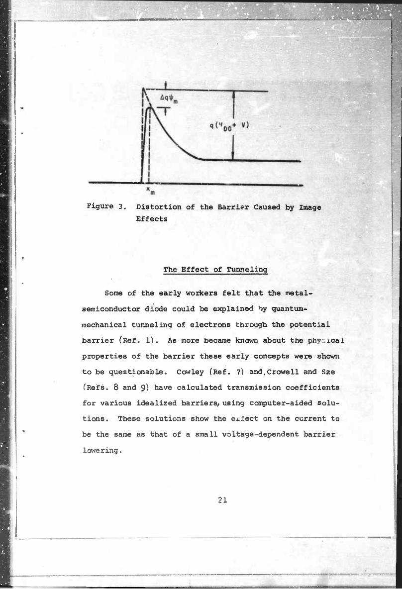
Figure 3, Distortion of the Barrier Caused by Image
Effects
The Effect of Tunneling
Some of the early workers felt that the metal-
semiconductor diode could be explained by quantum-
mechanical tunneling of electrons through the potential
barrier (Ref. 1). As more became known about the physical
properties of the barrier these early concepts were shown
to be questionable. Cowley (Ref. 7) and.Crowell and Sze
(Refs. 8 and 9) have calculated transmission coefficients
for various idealized barriers,, using computer-aided solu-
tions. These solutions show the effect on the current to
be the same as that of a small voltage-dependent barrier
lowering.
21
——————

On the other hand, Padovani and Stratton (Ref 10^
have developed a model for the Schottky barrier which has
a temperature-dependent conduction mechanism. At low
temperatures, the dominant conduction mechanism is field
emission with the center of the transmitted electron energy
distribution equal to the upper filled states in the con-
duction band. For higher temperatures, the conduction mech-
anism becomes a combination thermionic-fieId emission with
the center of the energy distribution somewhere above the
low-temperature case but below the top of the barrier.
Finally, at high temperatures the conduction mechanism
becomes thermionic emission as predicted by the more ele-
mentary theories.
padovani and Stratton*s reported data show good
agreement with the theory for Shottky barriers made from
22 Au-GaAs with an impurity concentration of 10 atom?7
raetexr or greater. Experiments performed with lightly
doped GaAs did not agree with the theory.
The Effect of Interfacial Layers
The model for the Schottky barriers used so far has
assumed an intimate contact between the metal and the semi-
conductor. The problem of creating a clean surface is
widely recognized. Most semiconductor surfaces will
22

1 I I
readily combine with oxygen to form an oxide. It is very
probable that the contact between the metal and the semicon-
ductor is not intimate. We will therefore investigate
the effect of an interfacial insulating layer on the
characteristics of the Schottky barrier diode. Goodman
(Ref. 11) has shown that barrier capacitance is changed
by the presence of an .interfacial layer.
Figure 4a shows a band diagram of a metal-interfacial
layer-semiconductor junction before contact and before
thermal equilibrium is achieved. A calculation by Cowley
(Ref. 7) shows that there is negligible bending of the
bands in the insulator due to nurface charges. We will
therefore assume straight bands with a slope determined
by applied electric field for the insulator. The result-
ant junction in thermal equilibrium is shown in figures 4b
and 4c.
As shown in equation 10, the surface charge in the
semiconductor with no bias applied is /
Qsc * £2*€sNDVDe>3 1/2 (10)
Figure 4c shows that
ro - Xt - * *vio + (X8 - Xt) + «JVJJO + (», - x.)
L - ¥s " + *fvio + W (H9)
23

•» - • —
T m
T
INSULATOR
METAL
4 D E
SEMICONDUCTOR
I.
7777, a) Before contact, not. in thermal equilibrium
b) Before contact, in thermal equilibrium
L
c) After contact, in thermal equilibrium
Figure 4. Metal-Insulator-Semiconductor Junction
24

By Gauss' law the electric field in the insulator. E._, iO' can be shown to be
Qsc . gWW io ° *_. T;
1/2
(50)
where
c- = the dielectric constant in the insulator,,
The electric field across the insulator can also be
determined from the potential, V.Q, across the insulator.
„ Vi0 q *9m " *V " VD0 Eio nr •— (5D
where
!? = width of the insulating region
Equating equations 50 and 51 and defining the constant
V, • W2Csq]*D
T2 (52)
we get
ft« - o m 'DO
1 /X" - + V, - V V, + 2v(-£ - o v (55)
Note that V* in equation 53 includes the effect of an in- DO
sulator between the metal and the semiconductor. Therefore,
it is not the same as that defined by equation 1.
25
• -•
r

As the interfacial layer width, W, decreases toward
zero, equation 53 approaches equation 1, the original
definition of V^, The potential across the interfacial
layer is /
Vi0 * + k (q>* * **] ' VIX>
io . -Vl + J^^-l*) (54)
In the presence of an applied potential, equation 49
becomes
** ' % + V = q(Vi + V <55>
Following calculations similar to those in the zero bias
case we can show that
VD q
+ Vx + V - VV* + 2V1 (v + " q *)
(56)
The potential across the interfacial region is given by
26

v- • h IVm " O + v - V. i q m Ts I
Vi = "Vl+ ^Vl + 2V1 (V + —q-^ ) (57)
where V- is given by equation 52.
The capacitance of the junction can be determined from
Ml. C -
sc W
and
Q sc - '-P- = ^ [ -vx *M * 2vx(v + 5L^lj]
By applying equation 58 to equation 59 and using equation
52 we obtain
C = *A
2V + 2 *m * *s + V.
1/2
(60)
which is similar to equation 11 with the addition of the
term in V .
The customary presentation of capacitance information 2
takes the form of a plot of 1/C vs V, which in this case
is siven by
27
— •

2"m 2 [V + Vi + ^] (6X) s"D
The V axis intercept occurs at
V = - JL^-1 - -* (62)
The interface effects a shift of the intercept toward the 2
-V or forward bias direction. The slope of the 1/C
curve, however, remains unchanged (i-e., inversely pro-
portional to $_).
If the *nterfacial layer is thin enough, it is reason-
able to assume that the interfacial layer is transparent
to electrons ^of sufficient energy to traverse the barrier.
The major effect of the interfacial layer upon the V-I
characteristics is therefore the change in the barrier
height, qVD-
Equation 17 was stated as
T kT 11/2 -*vD/kT
where
7 ss v + V *D VD0
28

In the presence of the interfacial layer, from equation 56
we can show that
vD - vM + v + fv? + ^.(SLf!- )]
[v2 + 2vx(v + ^_-^)]1/2 (S3)
where V^ is defined by equation 53» V--. with the inter-
facial layer is smaller than V-- without the interfacial
layer; therefore we can expect a higher leakage current.
V_ can be seen to be a slightly weaker function of V in
the presence of the interfacial layer.
The Effect of Surface States
The elementary Schottky barrier theory predicts that
the barrier height will be directly dependent upon the
work functions of the metal used as shown by equation 1.
Investigation of this property led to the classic paper
by Bardeen (Ref. 12) about the effect of surface states
upon barrier height.
The Model of Bardeen was adopted by Cowley (Ref. 7)
and Cowley and Sze (Ref. 13) to explain the dependence of
barrier height upon surface states. A band diagram of the
semiconductor with surface states is shown in figures 5*
29

a) Neutral surface, not in thermal equilibrium
*
i.
1 qV BO
9
V///////////K b) Negative surface cnarge, in thermal equilibrium
Figure 5. Free Semiconductor Surface with Surface Stat s
30

.ESBESBB.
and 5b» Figure 5a shews the semiconductor not in thermal
equilibrium; «p.. is the energy tc which the surface state«
are filled to obtain charge neutrality on the surface.
The surface states that are unfilled and below the Fermi
level must be filled for thermal equilibrium. Figure 5k
shows the bending of the energy bands when thermal equi-
librium is achieved.
A uniform distribution of surface states is assumed
above q>,. The density of states per unit energy per unit
area is given by N . From equation 10 the charge contained
within the space charge distribution is given by
QSC=V2*CsNDVB^ f64)
where
VBO = potential barrier height necessary for thermal equilibrium
The charge in the surface states, Q . can be expressed as ss
Qss --2q-Naf* - *n - ^ -qV^) (65)
The requirement for semiconductor charge neutrality is
satisfied by '
1 + Q „ = 0 'sc ss (66)
31

1
'
Whe When this condition is solved for v.- it yields BO
C-«i
BO + I (Eg • S • »i> + ZX2? 4q^N
" Ik (Eg - *n " O C.N s"D cA S2M 1/2
ZtfVj x4q^Ns
(67)
For large N _, equation 67 reduces to s
VBO " J (Eg " 9n - *1> (68)
The barrier height is fixed and the Fermi level is pinned
to 9, independent of bulk properties.
Formation of a metal contact is shown in figures 6a
and 6b. Before contact there is a potential difference
r f 1/q (9 - 9 ) - V__ which must be compensated for by
rearranging the charae. A potential drop across the inter-
facial region also exxsts. Overall charge neutrality requires
Q m _ (Q + Q ) wm vwsc ss' (69)
The potential across the interface can be determined
by two methods. From Gauss' law we get
32

1 •l
1
k.
777777/ a) Before contact
77777?. 7
7777T7T, b) Af-er contact
Figure 6. Metal-Insulator-Semiconductor Junction
with Surface States
53
m •

•'»•'»•I
mmmmmmmmmmmmm.
io Ci
Vio - -W Jj It follows front equations 64, 65, and 69 that
vio - 71 [(^.Vnp)172 * 2qNs (Eg -•«-•!- «Ü]
(70)
and from figure 6b
vio -f bm - *• - «"DO - \] (71)
Equating equations 70 and 71 and solving for V-^we get
j K - X. - »nW « (Eg - % - «j> Vl 00 (l + «q) (1 + aq)2
,7^7 [2(1 + ««) {J(*B-X. -V
+ «(I - »n - t.^} vl + v/J (72)
where
1 "57" 2WqN_
54

As the density of surface states becomes large the
barrier height given by equation 72 reduces to
DO K- n in)
which is the same as the fixed barrier height for a free
semiconductor surface with a high density of surface states
given by equation 68. When the number of surface states
is small, equation 72 reduces to
v DO q vym - *s - *n> + vl " V + I (<P
(74)
Equation 74 is comparable to equation 53 which gives the
barrier height in the presence of an insulating inter-
facial layer with no surface states.
A different ssrr.i-empirical approach to surface states
was proposed by Mead (Ref. 14). The following discussion
is similar to Mead's. For a more detailed and mathematical
analysis of the existence of surface states, see Grimley
(Ref. 15) or Shockley (Ref. 16).
Surface states apparently are caused by the termination
of the crystal lattice at the surface or by the presence of
adsorbed foreign atoms. In the Shockley model, surface
statas exist only for value« of lattice spacing less than a
35

critical value A (see figure 7)* One can argue that for
lattice spacing greater than A the surface " -.ates are near
the band edges. As the lattice spacing gets smaller than A
the surface states move rapidly toward the center of the
band gap.
When acceptor-xike states are introduced below the
Fermi level, they will not be in thermal equilibrium until
they become occupied. Some of the electrons in the con-
duction band will have to fall into these states. This
action causes a negative surface charge and a positive
space charge to develop. Consequently the energy bands
bend upward at the surface in a manner similar to that
described earlier for the metal semiconductor junction.
Acceptor states above the Fermi level will have no effect.
If we assume a semiconductor with a small lattice
spacing and a high density of surface states, its energy
diagram will look like figure 7. As a metal is brought
closer to the semiconductor interface, it will cause further
upward bending of the anergy bands. Any of the filled
surface states that are above the Fermi level will give
up their electrons to the metal when contact is achieved.
Therefore, the effect of the metal upon the barrier height
is limited. In materials with larger relative lattice
spacing and hence surface states closer to the valence and
conduction bands, the barrier height will be more Affected
56

oi
US
LATTICE SPACING, d
Figure 7. Energy Bands as a Function of Lattice Spacing
57

by metal work function. Mead and Spitzer (Ref. 17) have
found that for most group IV and III-V semiconductors the
Fermi level is fixed at a point approximately S /3 above
the valence band edge, where E is the width of the band
gap.
Mead's model for surface rütss can be mathematically
formulated by assuming that the surface states exist uni-
formly over a band of width <p« at a distance of (p, above
the valence band edge. Two possible band configurations
are illustrated in figures 8 and 9-
In f i'jüre 8
H DO < - 9« n (75)
The rer.ultant bending of the bands caused by the surface
states and the metal is insufficient to raise any of the
surface states in cp« above the Fermi level. The charge
in the surface states is
Qa, - -2qN '88 sy2 (76)
Tha charge in the depletion region is given by
V2qe A VT Qsc * V2qc."D 'DO (77)
33

•m
T,
w
a) Before contact
C
± y i
T qV BO
l
>/)////,
7777777, b) After contact
Figure 3. Metal-Insulator-Semiconductor Junction
With qV^ <Eg-»r»2-«n
39

nq
i m
'7 7777, w i_-
T
r
fc
r- c n E
///////' v
a) Before contact
.
'///////
b) After contact
Figure 9. Metal-Insulator-Semiconductor Junction
with qVD0^ Eg -•1-»2-*n
40

The charge in the metal is given by equation 69. Fran
consideration of Gauss' law and equality of potentials
as explained earlier, we get
?<•• " X8 - ^DO " *J m ^I'DO - «2 <W
where V. and ft are defined following equation 72
Solving equation 78 for V_- we get:
VD0 * k (% - \ - V + <*2 + Vl
In the limit as the number of surface states becomes
small, i.e., when a approaches zero, the barrier height, V^,
becomes
1, n—1——"— VD0 s q f*. * Xs ^ *J + Vx - VVl + 2 ^ - X8 - ^
(8D)
Equation 80 is comoarable to equation 53, the expres-
sion for V_D with the presence of an insulating interfacial
layer end no surface states. The barrier height increases
with surface state density. Therefore, the limit of this
case, based upon figure 8# approaches that depicted by figure
9 as the rumber of surface states becomes large.
41
-

In figure 9
^DOiEg-'n"'r *2 (Ö1)
The distortion of the energy bands will cause a portion of
?? to be above the Fermi level; therefore the surface
»tatea will not be completely filled. The charge in the
surface states is given by
- -2<3!a(Eg - 9X - *n - qVj^) (82)
This is the sane as equation 65 in the development of the
first mc I including surface states. The solution for the
second e of the model by Mead is the same as the solution
of the rri&r height for the first model proposed by
Bardeen.
Both models show that th* barrier height is a function
of the density of the surface states. In the limit, as the
density of states becomes large, the barrier height becomes
fix*d and independent of the metal work function.
42

Etfects of Minority Carrier Current
Studies of the minority carriers in Schottk; barriers
have been performed (Refs. 5 and 18). The conclusions ax«
that in a material where the majority carrier density is
much greater than the minority carrier density, the drift
and diffusion components of the minority carrier current
cancel each other almost exactly. When the majority carrier
current density is sufficiently high to cause an electric
field to be developed across the bulk material, a more
significant minority carrier current component can be
expected.
43
•»- • .I.. —'. • i ii

JWW wan
SECTION III
RADIATION EFFECTS ON SCHOTTKY BARRIER DIODES
In this section the effect of transient ionizing
radiation on Schottky barrier diodes will be considered.
First, it will be instructive to consider the basic inter-
actions of ionizing radiation with matter. Next, the effect
of ionizing radiation on a semiconductor will be discussed.
Finally, the previous discussions will be applied in the
determination of the effect of transient ionizing radi-
ation on Schottky barrier diodes.
Interaction of Ionizing Radiation with Matter
The ionizing radiation to be considered in this paper
consists of gamma rays produced by nuclear fission and
X rays produced by a high-energy pulsed electron source.
In both cases energy exists in the form of photons. These
photons interact with matter by four processes: photo-
electric, Compton, pair production and photodisintegration.
The photoelectric process tends to dominate for photons
of low energies (Z^QQKQV). The photoelectric effect is
the photon electron collision process whereby the incident
photon is completely absorbed in the collision. The
kinetic energy of the resultant photoelectron is dependent
44

upon its binding energy to tw atom and the energy of the
incident photon. The scattering cross section for the
photoslectric process* decreases with increasing photon
energy and increases with increasing z number of the
material.
The impinging photon may knock an electron from either
an outer or inner atomic shell. If an inner shell electron
is knocked out of its position, the atom emits a charac-
teristic X ray in the process of de-excitation.
The Compton effect results more often from a collision
of a somewhat higher energy photon and an electron. Ccmpton-
type collisions commonly occur for photon energies between
0.2 and 5 Mev. The result of this collision is an energetic
electron, a photon of reduced energy, and an atom with an
electron missing from the atom. On the average, the electron
energy is slightly less than one-half the energy of the
incident photon.
Pair production is a reaction that can occur when a
high-enargy photon interacts with the field of a charged
particle or nucleus. The energy of the photon is con-
verted into an electron-positron pair. For this change to
be possible, the photon energy must equal at least twice
the rest mass energy of an electron or 1.02 Mev Any
excess photon energy is shared as kinetic energy of the
electron-positron pair. The pair production process domi-
nates for high Z materials at energies above 5 Mev and at
45
•MM «111 ill» •-
higher energies for low Z materials. The recombination or
annihilation of a zero momentum electron-positron pair
results in two 0.$1 Mev photons going in opposite directions.
Collisions of high-energy photons (>10 Mev) with a
nucleus can cause ejection of protons, neutrons/and
^-particles. This process is known as photodisintegration.
Photodisintegration is not usually considered as an impor-
tant process because of the high energies necessary to
produce it.
We have now considered the processes by which photons
interact with matter. The results of these processes are
usually energetic electrons. Therefore, the interactions
of energetic electrons will now be discussed.
The electrons lose energy by collision, scattering,
and radiation. The creation of BremsStrahlung is impor-
tant for high-energy electrons with high Z materials. The
collisions are considered to be inelastic collisions with
electrons in atoms. Electron scattering is caused by the
simple Coulomb interaction between charged particles.
The energy spectrum of the resultant secondary electrons 2
is proportional to i/E . The higher-energy electrons of
the spectrum are capable of producing further ionization.
2 This second generation of electrons will also have a 1/E
energy spectrum The process will continue from gener-
ation to generation until none of the remaining electrons
46

.,—, . —,
has sufficient energy to cause further ionization. The
final distribution of electrons if independent of th«
primary processes involved.
Effect of Ionizing Radiation upon Semiconductors
Ionizing radiation when discussed in conjunction
with semiconductors is of low enough energy that photon
interactions by pair production and photodisintegration
can usually be neglected. Occasionally an electron cf
high energy can be created by the photoemission or Corao-
ton processes. If this electron suffers a collision with
the nucleus, the atom can be knocked out of its proper
location in the crystal lattice.
In silicon or germanium semiconductors this damage
results in a vacancy and an interstitial atom known as
a Frenkel defect. In a III-V compound semiconductor there
are eight possible defeccs caused by displacement or sub-
stitution. These defects are: two types of vacancy, two
types of substitutional defects, and four possible inter-
stitial configurations. Clearly, separation and cataloging
of the effects of these defects for compound semiconductors
are more difficult than for silicon or germanium. For-
tunately, the number of defects created ia typically small
when compared with the number of pre-irradiation defects.
Therefore, the problem of permanent damage is customarily
47

fmSi>M*«STO*>"«ra*• »*•' *W«
neglected in a study of the effect of transient ionizing
radiation upon semiconductor devices.
Our primary interest is in the effect of secondary
electrons created by the ionization process. Progressing
from the individual atom model to the band model of the
semiconductor, we find that the secondary electrons exist
as free electrons in the conduction band and a corresponding
number of free holes exist in the valence band.
Studies of gases and semiconductors in a radiation
environment have led to the conclusion that the number
of electron-ion pairs created in a material per unit of
energy deposited is only a weak function of the target
material (Ref. 19). For gases, an electron-ion pair is
created for an energy deposited equal to approximately
twice the ionization potential. The energy necessary to
create an electron-hole pair in a semiconductor is about
three to four ti!*9S the band gap.
Electrons and holes in a semiconductor material move
primarily under the influence of electric fields and den-
sity gradients. Mobility, u, describes the excess motion
of electrons and holes in an electric field. Mobility in
silicon is considered a constant for electric field strength
less than 10 volts/cm (Ref. 3). The diffusion coefficient,
D, describes the motion of holes and electrons by diffusion
under a density gradient.
48
The one-dimensional equations for hole and electron
current are given in equations S3 and 84. Since opposite
charges attract, we would expect the electron to move to-
ward a positive potential and the hole to move toward a
negative potential. These components of current that are
influenced by the electric field are commonly called drift
current. The diffusion current is a result of the spreading
of electrons or holes away from a concentration of carriers.
jn = q Un HE + q Dn §§ (&)
j =qU pE-qD $£ (84)
where
3 • electron current density
j * hole current density
q = magnitude of electronic charge
M = electron mobility
|i • hole mobility
n = electron concentration
p • hole concentration
E • electric field
D = elt-:. jron diffusion coefficient n
D • hole diffusion coefficient P
49

Electrons *»ncl holes will move as described in equations
82 and 84 until "-hey re combine.
Recombination by direct band-to-band electron-hole
annihilation is extremely rare, even in materials such
as GaAs where this phenomenon would seem to be highly
probable. Usually recombination occurs by a multistep
process. Defects in the semiconductor result in recom-
bination centers in the forbidden gap. These defects
will capture another one of the free carriers, say a hole?
then sometime later the defect will capture an electron
and annihilate it. Recombination can be treated mathe-
matically by a technique originally described by Hall
(Ref. 20) and Schockley and Read (Ref. 21).
Another process known as trapping will temporarily
immobilize electrons or holes. A trap is a defect with
a large capture cross section for one of the mobile
carriers. The trap will capture the carrier, hold it for
a finite time interval, and release it so that it may
again contribute to conduction. Traps may immobilize
carriers for time periods up to days in duration.
50

Effect of Ionizing Radiation upon Schottky Barrier Diodes
When a conventional p-n junction is irradiated, an
excess of free carriers is produced. The resultant current
is dependent upon the radiation pulse intensity and shape,
the minority carrier lifetime, minority carrier diffusion
length, and applied bias voltage. If the minority carrier
lifetimes are short compared to the radiation pulse width,
the resultan* current pulse will follow the radiation pulse
If the minority carrier lifetimes are long compared to the
radiation pulse width, the resultant currant pulse will
relax to its pre-irradiation value with a characteristic
time period.
Under irradiation, electron-hole pairs are generated
uniformly throughout the semiconductor. The carriers
created in the depletion region are immediately subject
to the influence of the relatively strong electric fiel'*
that exists across this region. The time necessary for
the carriers to be swept out of the depletion region is
usually much less than the radiation pulse width. To an
external circuit, the current created by the motion of the
carriers across the depletion region will appear to be
instantaneous.
Usually, the percentage change in majority carrier
density is much less than the percentage change in the
minority carrier density. This causes larger carrier
51

gradients to exist for the minority carriers. Therefore,
the minority carriers will dominate the diffusion con-
tribution to the total current.
Mcbt of the radiation-induced diffusion current will
be du° r.o excess minority carriers produced within a
diffusion length on either side of the junction. Radiation
induced current will flow in a direction so that it will
aid leakage current and oppose normal forward current flow.
The movement of the excess -arriers is determined by the
one-dimensional continuity equations (equations 85 and 86).
ft n - n o
n 4- i-i- j + g q *x Jn * (85)
if 5^2-iLj +q T„ q 3x Jp
(86)
where
n * thermal equilibrium density of electrons
p • thermal equilibrium density of holes
g = generation rate of hole-electron pairs due to an extern"" source
T = minority carrier lifetime for electrons 'n
r • minority carrier lifetime for holes P
The continuity equation reflects the time rate of change in
carrier density caused by thermal generation and recombi-
nation, outward flow of current, and radiation generation.
mv*mmmmmmmma m WMLUII
Substituting equations 85 and 84 into equations 85
and 86 we get
5t Tn n 77 ln ax (87)
Po " + D 2_ p M_ Isf (PB) * g (83)
Equations 85/ 84, 37/ and 88 have been solved by Wirth and
Rodgers (Ref. 22), van Lint (Ref. 19), et al. assuming
uniform doping concentration, an electric field free region
and a rectangular pulse of radiation, the solution is
ipp(t) - q Ag [(i + Lnerf Vt/Tn + Lperf Vt/Tp)u(t)
t + Ln erf V(t-to)/Tn + L erf V(t-t0)/r )u(t-t0) j
(89)
where
i (t) = radiation-induced photocurrent PP '
h
t
= junction area
= depletion layer width
L = \/b T = diffusion length for electrons n n 'p 3
L • ^D T = diffusion length for holes P P P
55

Xj(t) and Uft-t ) • unit step function turned on at o c
t - 0 and t - t , respectively
Recalling equation 19
2TT m
1/2 -qV^/kT (VqVAT . t] ri9,
we can see that the Schottky barrier diode is a majority
carrier device. Since the percentage change in majority
carrier density is much less than the percentage change in
minority carrier density, one would expect a majority
carrier device to be less affected by radiation than a
minority carrier device. This is the primary reason for
making a study of Schottky barrier in a radiation environment
Figure 10 depicts a Schottky barrier after exposure
to ionizing radiation. The excess carriers generated in
the depletion region will be swept out by the electric
field. These carriers will contribute to the prompt or
drift component of the photocurrent. Excess holes created
in the bulk region will have a gradient causing a diffusion
toward the junction. On the average, holes within a
diffusion length of the depletion region will contribute
to the diffusion component of the photocurrent. ft gradient
of electron concentration will not ^xist on the metal, so
no electron diffusion should be expected. From the previous
discussion of the p-n junction the resultant photocurrent
in the Schottky barrier diode should be
54
.. . w,.,, ,.„lau ,1 I .........
El
0
0
Jt -B£»j
Figure 10. Schottky Barrier During and Immediately
After Ionizing Radiation Pulse
55

. _
ippft) = q Ag I + L erf J&r) V(t)
- (t + L erf ^(t-t H ) U(t - tjl \ p O /f.-' o J W
The transient radiation does not affect the parameters
of the basic current equation for the Schottky barrier
diode. However, a permanent change in the barrier can be
caused by a charge trapped in the surface oxide. This
mechanism is illustrated in figure 11. During irradiation,
electron-hole pairs are created in the oxide. Making the
usual assumptions that the holes in the oxide are immobile,
the electrons will be attracted to the metal, leaving a
net positive charge in the oxide at the semiconductor
interface. This charge can cause a distortion in the
field configuration in the depletion region. Bell Tele-
phone Laboratories (Ref. 2'$) noted a small variation in the
characteristics of Schottky barrier diodes after heavy
irradiation.
A gamma dose of 10 rads from a Co source was found
to change the reverse leakage current of an Au-Si diode
-8 -5 at 5 volts reverse bias from 5 x 10 to 10 ampere.
This dose level is well above those considered in this
report; therefore, no further consideration of this effect
will be made.
'36

+ + + + + + + +
«NM- O — + in
+ + + "N
CO
+ J +
UJ
z 1 o + . t- + < M + — + _l + < 1- 4-
3C + +
s •H
> •H
CO m
•0 •H
o
5
G O
-H 4J «0 H 3
Ü U
(1)
X! U
57

SECTION IV
EXPERIMENTAL RESULTS
Diode Characteristics
The Schottky barrier diodes used during the experi-
mental portion of this study were produced by Texas Instru-
ments Inc., and have Texas Instruments part numbers TIXV19
and TIV305. The TIV305 is a metal-silicc7 Schottky barrier
diode mounted in a small hermetically sealed glass package.
The diode is designed to operate as a UHF mixer. The
TIXV19 is a metal-GaAs Schottky barrier diode mounted in
a Type E microwave package. The diode is designed to
operate as an X-band mixer.
Extensive measurements were performed upon the diodes
to determine the diode parameters necessary for prediction
of the diode response to an X-ray pulse. The junction area
was determined by breaking the top off the diode packages
and using a microscope to measure the diode geometry. The
TIXV19 had a circular junction with a diameter of 10.5 x 10 -6
meter and a circular bonding pad of 27.^ x 10" meter in
diameter as shown in figure 12a. The TIV305 has a circular
junction that is 30.55 x 10" meter in diameter and a
circular bonding pad that is 126.3 x 10" meter in diameter,
as shown in figure 12b.
58

— 11 in • •»if. —
JUNCTION AREA
a) TIXV19 Geometry
JUNCTION AREA
b) TIV305 Geometry
Figure 12. Schottky Barrier Diode Geometries
59

The capacitance-voltage characteristics were mea-
sured for each type of diode using a Boonton Model 75A-S8
capacitance bridge. A capacitance-voltage plot was made
for each diode on a semi-autcmatic capacitance measuring
system borrowed from Sandia Corporation. Typical curves
are shown in figure 15.
The package capacitance was subtracted from the
capacitance-voltage curves and the resultant data were 2
used to create plots of 1/C vs V. These plots are shown
for the TIXV19 and TIV305 in figures 14 and 15, respec-
tively.
Before attempting determination of the barrier height
and doping concentration from figures 14 and 15/ the con-
struction of the diodes should be taken into consideration.
Equation 9 shows that the maximum electric field is pro-
portional to the majority carrier doping concentration ND.
Therefore, in order to achieve a high reverse breakdown
voltage, a diode should be made from a material of low
dopant concentration. An increase of dopant concentration
will decrease the series resistance of the diode; this is
also desirable.
These conflicting requirements on N are resolved in
the case of the TIXV19 and TIV305 by growing a thin lightly
doped epitaxial layer on top of a heavily doped substrate
as shown in figure 16.
60

'••""• J"W
<T\
0.5
V R,
volts
Figure
13*. Capacitance versus Voltage for T1XV19 and TIV305 Diodes
p ••MMMBMBV

C (f/m )
1.0
-1.0 1.0 2.0 3.0
V , volts
k.O
Figure 14. 1/C versus V for a TIXV19 Schottky Barrier Diode
r^

1 •• "*' • '.IP* ••• DPpn«iMin»> vrprmj^jUQp^-
C2 (f/m2)2 x 10
-1 ,0
i
1 .0 k.O 2.0 3.0 V , volts
Figure 15. 1/C2 versus V for a TIV305 Schottky Barrier Diode
65

—sA»fi—
ft
METAL
OXIDE
n EPITAXIAL LAYER
n+
SUBSTRATE
Figure 16. Construction Profile of a
Typical Schottky Barrier Diode

rv* • —
-' ;
•
Impurities diffuse from the heavily doped substrate
into the lightly doped epitaxial layer during the epitaxial
growth process, creating a finite impurity gradient. This
2 impurity gradient is the reason that the 1/C vs V plots
are not linear«
Equations 12 and 13 in conjunction with figures 14
and 15 can be used to determine the barrier height, V-^.
and the dopant concentration, N_.. Restating equation 12,
? 7J& *m + v) (12}
o we recall that V = -V when 1/CT = 0.
An extrapolation of the curve in figure 14 gives a
V axis intercept of -4.06 volt, which does not compare
favorably with barrier heights of 0.94, 0-95, and 0.97
volt given in references 24, 17/ and 25/ respectively.
similar extrapolation in figure 15 results in a barrier
height of 0.77 volt which compares favorably with the
values of O.78, 0.79* and O.8O volt given by references
17/ 26, and 27/ respectively.
d(l/CZ) H3V W (13»)
65
•A..,, ,,„^.
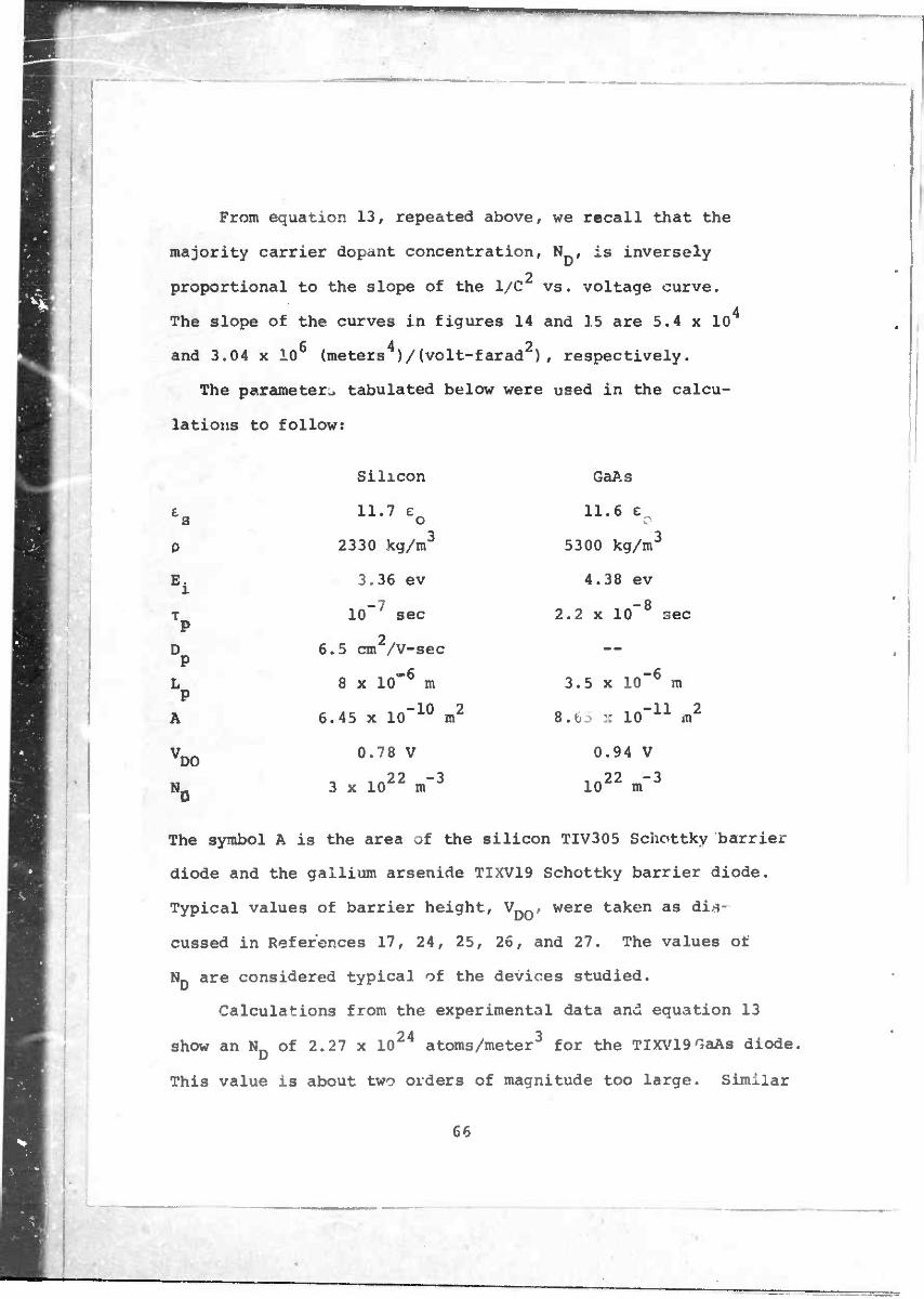
From equation 13, repeated above, we recall that the
majority carrier dopant concentration, N_, is inversely
2 proportional to the slope of the 1/C vs. voltage curve.
The slope of the curves in figures 14 and 15 are 5.4 x 10*
6 4 2 and 3.04 x 10 (meters )/(volt-farad ), respectively.
The parameters tabulated below were used in the calcu-
lations to follow:
E,
P D
A
V, DO
N.
Silicon
11.7 e o
2330 kg/m3
3.36 ev
10"7 sec
6.5 cm /V-sec
8 x 10"6 m
-10 2 6.45 x 10 iU nT
0.78 V
22 -3 3 x 10 m °
GaAs
11.6 e., o
5300 kg/m3
4.38 ev
2.2 x 10"8 sec
—
3.5 x 10"6 m
-11 2 8.b_> :: 10 J"L iti
0.94 V
1022 m"3
The symbol A is the area of the silicon TIV305 Schottky barrier
diode and the gallium arsenide TIXV19 Schottky barrier diode.
Typical values of barrier height, V_Q, were taken as dis-
cussed in References 17, 24, 25, 26, and 27. The values of
ND are considered typical of the devices studied.
Calculations from the experimental data and equation 13
show an NQ of 2.27 x 1024 atoms/meter3 for the TIXV19 GaAs diode
This value is about two orders of magnitude too large. Similar
66
, -—,—
MananauMN
22 3 calculations give an Nn of 3.98 x 10 " atoms/meter for
the TIV305 silicon diode, which is the proper order of
magnitude.
The discrepancies between the expected and measured re-
sults for the TIXV19 diode are a result of inaccuracies
inherent in the measurement of their capacitances. The
Type E microwave diode package has a nominal capacitance of
5.5 x 10~ farad. The calculated capacitance of an ideal-
ized GaAs Schottky barrier diode with a junction area of
8.65 x 10~ meter2 is 4.2 x 10~ farad. The capacitance
of the Schottky barrier diode and its variation with volt-
age is two orders of magnitude smaller than the capacitance
of the package alone. Therefore, it s impossible to re-
solve the true capacitance variation of the GaÄs diode ca-
pacitance with voltage because of the much greater package
capacitance.
The calculated capacitance of a silicon Schottky
-10 2 barrier diode with a junction area of 6.45 x 10 meter
is 3.68 x 10 farad at zero applied bias voltage. TL»
package in which the diode is mounted has a capacitance of
-13 approximately 3.5 x 10 fc»rad. Although the ratio of di-
ode capacitance to package capacitance is far from ideal, it
is reasonable that better correlation was obtained between
measured and calculated values for the TIV305.
Typical current voltage curves are shown in figures 17
and 18 for the TIXV19 and TIV305, respectively. The deviation
67
—- —_—^____

I »• I II 1 - - I I I I
10 -2
to -3
10 -i»
n e u o a E
10 -5 .
10 -6
10-7
V FORWARD
Figure 17. Current versus Voltage for a TIXV19 Schottky
Barrier Diode 68

Figure l8. Current versus Voltage for a TIV305 Shottky
Barrier Diode
69

from a straight line at high currents is caused by the
series resistance of the diode. The deviation at low cur-
rents is not reproducible and is apparently caused by sur-
face conditions.
The peak photocurrent can be predicted by use of
equation 90
ipp - q Ag {(l + Lp erf Jt/Z ) u(t)
90^
The generation rate* g, is calculated from equation 91
g - 6.25 x 10 16 R
(91)
where
R * dose rate in rads/sec
p = density of material irradiated in kg/m
E. * energy necessary to produce one electron-
hole pair in electron volts (this is assumed to be about three times the forbidden band gap energy.)
T*ie dose rate at which the silicon and gallium arse-
nide Schottky barrier diodes were exposed was approximately
8 6.7 x 10 rad/sec or 20 rads in 30 nanoseconds. The calcu-
28 lated generation rates for GaAs and silicon are 4.2 x 10
70
i

28 3 and 2.9 x 10 electron hole pairs/second-meter , respec-
tively. These calculations were based on equation 91.
Note that equation 90 consists of two types of terms. The
terms which depend upon I arise from the photocurrent gener-
ated within the depletion region and is called prompt photo-
current. The terms which depend upon L arise from the dif-
fusion of holes from the bulk region of the semiconductor
to the metal/semiconductor junction. According to equation 90,
the photocurrent current will be a maximum at t = t", the
end of an assumed square wave radiation pulse, and is the
sum of the prompt and diffusion components of photocurrent at
that time. For our calculations t • 30 nanoseconds. o
From equation 4, the depletion width of the TIXV19 GaAs
diode is 3.47 x 10~ meters at zero bias. This calculation
22 3 is based on a doping concentration N_ • 10 atoms/meter .
Using equation 90, and the tabulated parameters for the
TIXV19 diode, the prompt, diffusion, and maximum photocurrents
are 0.2 x 10" ampere, 1.8 x 10" ampere, and 2.0 x 10" am-
pere, respectively. The value of T as tabulated was obtained
from reference 28.
A similar calculation for the silicon TIV305 diode yields
prompt, diffusion and total photocurrents of 0.5 x 10" ,
13.5 x 10~ and 14.0 x 10 amperes, respectively. The value
of ND used in determining the parameter I was 3 x 10
atoms/meter , a value typical of this device.
22
71
———
_•_- —••

It is interesting to compare theoretical maximum
photocurrents for GaAs diodes and silicon diodes of the
same junction area using doping concentrations typical
of the TIXV19 and TIV305. It follows from equations 4,
90, and 91 and the stated parameters of these devices that
the photocurrent of the GaAs diode would be 1.07 times the
silicon diode photocurrent, for a given dose of flash X rays
of 30 nanoseconds duration. If the dopant concentrations
were the same, this factor would become 1.16. We conclude
that silicon and gallium arsenide Schottky barrier diodes
should produce photocurrents per unit junction area which
are about the same value for a given dose and dose rate and
for the parameters typical of the TIXV19 and TIV305 diodes.
72

Results of Tests Using Flash X-Ray Machine
The experiments covered in this section were performed
at Kirtland Air Force Base, Air Force Weapons Laboratory,
using a Field Emission Corporation Febetron Model 705 two-
million-volt pulsed radiation source. A detailed description
of the source, test facilities, and equipment is contained
in Appendix II.
The TIXV19 GaAs Schottky barrier diode was tested as
a conventional diode» as a detector diode, and as a mixer
diode. The TIV305 silicon Schottky barrier diode was
tested as a conventional diode. The voltage-current char-
acteristics were monitored periodically during testing.
The noise figure of the diode was monitored while it was
being tested as a mixer. Dosimetry was obtained from the
thermoluminescence of lithium-fluoride-impregnated teflon
disks.
Testing of the diodes as conventional diodes was
performed,using the circuit shown in figure 19. In a
typical test configuration all of the circuit except the
diode under test was shielded from the X-ray beam by at
least 4 inches of lead. Spurious effects were minimized
by keeping all wirelengths short and decoupling the
power supply.
73
.•I ,

' «-•
'•'
"'•
••
I'II
WW
IKIW
WP
^M
I*«
-«-
nH
BM
I ••
'
ar-
v cc
50
H
V\A
A
DIODE UNDER TEST
KEITHLEY MODEL
103 OR 11
1
AMPLIFIER
TEKTRONIX
MODEL 517
OSCILLOSCOPE
Figure 19. Conventional Diode Test Circuit

The TIXVI9 GaAs Schottky barrier diodes were connected
as shown in figure 19 by means of a waveguide diode holder
and were exposed to an X-ray pulse of 3 x 10 second duration.
Total dose of a single pulse was approximately 20 rads. The
resultant peak photocurrent was 1.99 * 10 ^ and 3 x 10
ampere for reverse bias voltages of 1.0 and zero volts,
respectively. The peak photocurrent was two to three orders
of magnitude larger than the 2.13 x 10~ and 2.09 x 10 ' am-
pere predicted by equation 90.
The waveguide diode holder was removed from the circuit
and the diode was connected into the test circuit by
soldering. The resultant peak photocurrent was changed to
1.0 x 10 and 8.7 x 10" ampere under th-a same bias con-
ditions. Typical waveforms are shown in figures 20 and 21.
The TIV305 silicon Schottky barrier diodes were exposed
to similar X-ray pulses. The resultant peak photocurrent
was 2.30 x 10""^ and 2.28 x 10 ampere for a reverse bias
of 1.0 and 0.0 volt, respectively, as shown in figure 22.
These values are also considerably larger than the expected
values of 1.44 x 10"^ and 1.4l x lO"^ ampere.
The difference between the expected peak photccurrent
and the expeiimentally observed peak photocnrrent was too
large to be explained by normal experimental or equipment-
induced errors. Therefore an extensive testing program
was undertaken to isolate the source of the excess photo-
current.
V5

^ ^•s.
L / ^
V. /
i
a) TIXV19-1
VR«1.0
Horizontal 2Ons/cm
Vertical 20mv/cm g
Dose rate = 6.7 x 10 rads/sec
b) TIXV19-1
VR = 0.0
Horizontal 20ns/cm
Vertical 10mv/cm
Dose rate = 6.7 x 10 rads/sec
Figure 20. Response of GaAs Schottky Barrier Diode in
Waveguide to X-ray Pnlse
76
1' -'

i j
a) TIXV19-3
VR = 1.0
Horizontal 20ns/cm
Vertical 20mv/cm 8 Dose rate = 6.7 x 10 rads/sec
0£m
\ j \ / \ /
b) TIXV19-3
VR « 0.0
Horizontal 20ns/cm
Vertical 20mv/cm B
Dose rate « 6.7 x 10 rads/sec
Figure 21. Response of GaAs Echottky Barrier Diode to X-ray Pulsö
77

I——•*•—•« I IM
ft) TIV305-1
VR - 1.0
Horizontal 20ns/cm
Vertical 50mv/cm 8
üose ratt. 6.7 x 10° rads/sec
\
\ ^ jf
b) TIV305-1
VR -0.0
Horizontal 20ns/cm
Vertical 50mv/cm Dose rate = 6.7 x 10° rads/sec
Figure 22. Response of Silicon Schottky Barrier Diode
to X-ray Pulse
8
78

One of each of the two types of diode packages that
exhibited more than 10 ohms between its terminals was
obtained. The packages were obtained by subjecting a good
diode to a current surge from a discharging capacitor.
The resultant package, when irradiated, was expected to
behave in the same manner as before except that any contri-
bution from the diode junction had been eliminated. The
peak photocurrents obtained experimentally from the packages
were very nearly identical to the results obtained from
good diodes.
Insertion of 4 inches of lead between the package
under test and the X-ray source eliminates the photocurrent.
This shows that the photocurrent is a direct or indirect
result of the radiation.
Further experimental testing showed that a similar
photocurrent could be obtained by extending a wire about
0.75 inch long into the X-ray beam.
The photocurrent was of the polarity that required
electron flow from the test wire through the viewing
resistor to ground. Several possible sources of the spurious
signal exist. Possible sources ir^lude collection of
electrons knocked out of adjacent materials, the large
electromagnetic pulse that exists during the creation of
the X-ray pulse, ground currents, transients induced on
the power line, etc.
79

Because of the spurious response that exists in any
experimental test configuration, the only way to exper-
imentally prove the validity of equation 90 is to test
diodes whose true response is greater than the spurious
response. In the case of Schottky barriers, the peak
photocurrent can be increased by increasing the junction
area or by decreasing N«. Neither of these solutions can
be tried at this time because The University of New Mexico
does not currently have facilities capable of producing
Schottky barrier diodes and because the cost involved in
having an outside source produce Schottky barrier diodes
to our specifications is prohibitive.
The TZXV19 GaAs Schottky barrier diode was also tested
as a detector. The test circuit is shown in figure 23. The
oscillator output was set at 9*375 GHz and 1.0 y \Q~ watt.
The photocurrenl: was determined as a function of applied
bias voltage ar.d current. The sliding short was adjusted
to obtain a maximum DC voltage out of the detector for
each bias condition. The AC transient caused by the X- ray
pulse was *hen observed.
The peak photocurrent as a function of applied bias
was approximately the same as before, without the microwave
signal. The peak photocurrent as a function cf DC bia«
current is shown in figure 24.
80

—"—"
•'-.
r
ftlA
S SUPPLY
SLIDING
SHORT
11 DIODE
UNDER
TEST
VIEWING RESISTOR
AMPLIFIER, OSCILLOSCOPE
MAGNETIC
ISOLATOR
10 db
DIRECT90NAL
COUPLER
FREQUENCY
METER
—
POWE
-
NETE
ft
—
MAGNETIC
ISOLATOR
LFE
MODEL
8UA-X-21
MICROWAVE
OSCILLATOR
Figur« 23«
Circuit for Testing GaA« Sefcottky Barrior
Diode as an X-b*nd Dotr -tor Diode

••""""
•""—'''"•
'••
-—
•
^
"M
•••
s
0.1 0.
2 0.
3 0.
1» 0.
5 Ü.
6 0.
7 0.
8 0.9 1.0 1.
1 1.2 1.5 I»* 1.5 1.6 1.7
bias
ma
Figure *
24. Peak Photocurrent versus Bias Current fo
r Detector Diode

h A minimum peak phot©current occurs between 9 x 10
and 1.3 x 10 f ampere forward bias. The minimum occurs
only when the microwave signal is present.
The TIXV19 GaAs Schottky barrier diode was also tested
as a mixer diode. The test circuit is shown in figure 25.
A magic tee was used to mix the signals from the two signal
generators. A microwave signal entering the E arm of the
magic tee is split in tvo parts with half of the signal
going into each of the straight-through arms and no signal
coupled into the H arm. Conversely, a signal entering the
H arm is split with no coupling to the S arms. Magnetic
isolators were used in each arm to prevent propagation
of reflections back into the magic tee. The local oscillator
was set at a frequency of 9-375 GHz with a power at the diode
of 1.0 x 10"^ watt. The oscillator in the antenna leg
was set at a frequency of 9-405 GHz or 9-3^5 GHz. The
power level was adjusted to achieve a predetermined signal
out of the mixer diode.
The mixer diode was connected to a DC bias source and
an I-F amplifier with an input impedance at JO MHz of 50
ohms. The amplifier has a gain of 48 db, a center frequency
of 30 MHz, and a bandwidth of 8 MHz.
For noise figure measurement the antenna leg oscillator
was replaced by a Hewlett-Packard Model X-3^7A noise source.
The output of the amplifier was then fed into a Hewlett-
Packard Model 3^2A noise figure meter. The noise figure
83
•

^^^
'"•' "
'-«'
—M"w
>«»>•
BIAS
SUPPLY
AMPLIFIER
OSCILLOSCOPE
SLIDING
SHORT
DIODE
UNDER
TEST
* MAGNETIC ISOLATOR
LOCAL OSCILLATOR
»-- T'f-.l
I
l I
I .1
-I LFE MODEL 8UA-X-21
MICROWAVE OSCILLATOR
FREQUENCY
METER
ANTENNA
HEWLETT-PACKARD
MODEL 624A
MICROWAVE OSCILLATOR
Figure 25
. Circuit for Teeting GaAa Schottky Barrier
Diode as an X-band Mixer Diode
POWER
METER
was checked before and after irradiation of the diodes.
No change in noise figure was observed.
Before each X-ray pulse the antenna leg oscillator
was adjusted between -45 dbm and -60 dbm to provide a
20 x 10 volt signal out of the I-F amplifier. The exact
power setting was a function of the bias current applied
to the diode under test. A typical output waveform is
shown in figure 26» The change in maximum peak to peak
amplitude as a function of bias current is shown in figure
27« An input of approximately 8 x 10"^ ampere is necessary
to obtain an output from the amplifier of 1 volt.
The 30 MHz amplifier, because of its 8 MHz bandwidth«
-7 has a rise time of approximately I.I5 x 10 ; second. The
output waveform (figure 26) is apparently the response of
the amplifier to a narrow pulse that coincides with the
X-ray pulse. This serves to illustrate one of the problems
that will be encountered by receivers with narrow band-
width I-F amplifiers in a radiation environment.
No changes were observed in any of the steady-state
parameters of the diodes after irradiation. The noise
figure remained constant. The V-I characteristics did not
change. The diodes were exposed to a neutron gamma flux
at the Sandia Pulsed Reactor II. Details are given in
Appendix HI.
85
* ' " "SS

"—
f\f\>
I
I \
TIXV19-1
I--1 ma
Horizontal J00ns/cm
Vertical 200mv/ctr.
Figure 26. Response of OaAs Schottky Barrier Diode Operating
as a Mixer Diode to an X-ray Pulse as Seen at the
Output of the I-F Amplifier
86

!-
oo
VI a
0.9
o a0'8
0.7
0.6
0.5
Zix
via-
3
TIXV19-1
>
i J
1 L
j
1
|
0.1 0.2 0.
3 0.
4 0.
5 0.6 0.
7 0.
8 0.9 1.0 1.
1 1.2 1.3- 1.4
1 .5 1.6
bias
' p»
a
Figure 27. Maximum Peak to Peak Voltage versus Bias Current
for
TIXV19 X-band Mix r
Diode

In summary, little can be said about the behavior of
the Schottky barrier junction in a radiation environment.
The response of the junction is masked by spurious response
of the packaging and the surrounding environment.
Tnis same limitation has been reached in experiments
upon other types of devices. Further work can be done with
larger junctions as they become available. In the long
run, a more meaningful study would determine the sources
of the spurious signals and develope techniques for their
elimination.
•
88
APPENDIX I
DERIVATION OF VELOCITY DISTRIBUTION OF ELECTRONS FROM FERBG-DIRAC DISTRIBUTION
The velocity distribution of electrons can be developed
frons the Fermi-Dirac distribution function.
«xp V-T5-; -1
If we assume a nondegerserate semiconductor and we are inter-
ested in an arbitrary energy A above the conduction band, we
can say
let
E = Ec + A (1-2)
?nd
E + A - E. » kT (1-3) c r
89

The Fermi-Dirac distribution function is now given by
-(B - E- + A). (1-4)
If we assume a lightly doped semiconductor, then N $ the
density of quantum states in the conduction band, is greater
than NL, the concentration of donor atoms. N is given by u c
•c - 2 [• 2 T m» kTl ^—J 3/2
(1-5)
The Fermi level in the semiconductor is given by
N E- • E -kT In f c I D
(1-6)
Nc E„ - E- • kT In «=r c f ND (1-7)
We now see that
f(E) - exp (-AAT) exp (-ln-jjS) aD
ND f(E) -^ exp (-AAT)
c
(1-8)
(c-9)
90

Substituting for N 3 c 3
f (E) = |- (2Trm*kTf3/2 Nß exp (-AAT) (1-10)
Digressing, we need to show that the density of states
per unit volume in momentum space is 2/h . Assuming a peri-
odic lattice structure and a parabolic energy momentum rela-
tionship, we can state
r,2 *A2 E - fer - y- (i-ii)
where
p = fek
and
k-j-ii
where the vector n is defined by
" " Vx + Vy + **n*
The quantities n , n , and n may assume both positive and
negative integral values. Therefore equation I-ll becomes
E = *1UL CI-12) a* 2m*
A yolume in n space is
4 3 V - 2 • JTT n (1-13)
91

This volume is also Na , the number of states included within
this spherical volume
N . M (£)5 (1-14) T a
It can be shown from the relations k = —- n and p = hk
that
r? - (fc)' (X-15)
Substituting equation I-15 into equation I-l4,we get
N=^ (1-16) 3H3
aN^^idp (1-17)
Dividing by the volume of a spherical shell in p space and
multiplying by a rectangular cartesian p-space volume
element, we get
dN * •£, dp dp dp (1-18) h* * y
92
—_ ,

dB _ 2 dpxdPydpz • -J d-19)
Now we can write the particle energy distribution per
unit volume in momentum space as
f(E>~3 = ND(2•* kT)"3/2exp (-VkT) (1-20)
Again assuming the parabolic energy momentum relation-
ship, let
A =
2 2 2 P + P + P rX *y Z
2m* (1-21)
ÜlJdN dpxdpydpz
2 2 2 -z/1 P + P + P
= (2^kT)^/2 exp (-Px2ra;yT
Pz) (1-22)
Integrating over all p + p y z
«a . (2•.*»)-W «p ( 2ra*kT,/ (1-23)
93

m • i MI ' **
Changing variables from momentum to velocity, we get
i1/2 , m*v2 N
This is the same as equation 14 in the text
94

APPENDIX II
EXPERIMENTAL FACILITIES AND EQUIPMENT
All of the X-ray testing was done at Kirtland Air Force
Base, Air Force weapons Laboratory, with Air Force-supplied
equipment. The X-ray source was a Field Emission Corporation
Febetron Model 705* The Febetron is capable of producing
a maximum X-ray dose of 3600 roentgens at dose rates up to
1.8 x 10 r/sec. The X-ray pulse is triangular and approxi- -Q mately 17 x 10 w second wide at the half peak intensity
points.
The testing was done inside a double-walled copper
screen room. Figure 28 shows a typical test configuration.
All of the circuit except the diode under test is shielded
from the X rays by at least 4 inches of lead. The viewing
resistor was selected as 50 ohms to properly terminate the
RG58 coaxial cable used throughout for signal transmission.
Amplification or impedance matching was provided by Keithley
Model 109 and Model 111 pulse amplifiers, which have 20 db »
and 0 db voltage gain, respectively.
A Tektronix Model 517 oscilloscope was used in con-
junction with a Model C19 camera to record all transient
signals. A variable attenuator was used at the oscilloscope
to provide gain control and impedance matching.
95

""•
<
<.*m
m&
mm
mm
riim
m
• •"'
'•!' "••"
•:.l»i-IW.'
«7>
££$53
*s*~
+t*'
• *'' •''.•',
rr-'W
. _ *
••
TEKTRONIX
MODEL 517
OSCILLOSCOPE
SCREEN ROOM WALLS
8' Rg58
KEITHLEY AMPLIFIER
MODEL 10
9 OR 11
1
T
50Q
«: /
Figure 28.
Typical Test Configuration Showing Screen
Room and Flash X-ray Machine

«*»
Inside the screen room, at a distance of approximately
8 inches from the wall, the dose received by tue diode under
test was approximately 20 rads. Other dose levels were
obtained by changing the position of the diode*
97

—.—
APPENDIX III
RESULTS OF NEUTRON TESTING OP SCHOTTKY BARRIER DIODES
The effect of neutron bombardment upon Schottky
barrier diodes was investigated. The diodes were tested
at the Sandia Pulsed Reactor (SPR) II. The SPR II is
capable of producing a neutron f luence of 5 x 10 ^ nvt Q
and a gamma dose rate of iCP R/sec at its outside surface. 14 A f luence of 5 x 10 nvt can be obtained by positioning
the components under test inside the "glory hole." The
glory hole is a 1.5-inch-diameter hole that extends into
th° center of the reactor.
Five of the WW19 GaAs Schottky barrier diodes and
five of the TF/3O5 silicon Schottky barrier diodes were
tested. The diodes were exposed to a total fluence ranging
from 9 2 x IO15 to 1.2 x IO15 nvt.
The original test configuration was designed to mon-
itor transient annealing of the diodes. No transient
annealing was observed. The gamma burst dominated the
response for at least 10 second after each burst. After
more time had elapsed, the diode was found to be undamaged.
The remainder of the tests were performed without real
time measurements. The tests consisted of measuring
98
the current voltage characteristics of the diodes before
and after irradiation. The current was measured over a
-7 -2 range of 10 ' to 10 ampere.
The test results for the TIXV19-7 GaAs Schottky
barrier diode are shown in figure 29« The curve labeled
0 gives the V-I characteristic before irradiation. Curve 1
is the characteristic after the first burst, with fluence
of 9.76 x 10¹⁵ nvt. Curves 2, 3, and 4 are the V-I char-
acteristics after the second, third, and fourth bursts,
with fluences of 1.12 x lO1^, 4.5 m lO1^, and 4,92 x 101*
nvt, respectively.
The curves shown in figure 29 were not called typical
because the change of the TIXV19 characteristic was not
consistent from diode to diode nor from burst to burst«,
The slope of the V-I usually increased; however, this was
not always the case. The slope for the TIXV19-7 increased
for all bursts except burst J.
The following generalisations can be made about the
TIXVI9 GaAs Schottky barrier diode exposed to a fluence
of 10 ' nvt or less:
1. The forward V-I characteristics do not change
-4 for currents larger than 10 ampere.
2. The forward V-I characteristics show a lower
resistance for currents less than 10" ampere.
3. The diode reverse leakage current increases
slightly.
99

IQ 0 0.2 Q.k 0.6 0.8 1.0 1.2
0.5 1.0 1.5 2.0 2.5 3.0 *
Figure 29, TIXV19-7 V-I Characteristics Before and After
Exposure to Neutrons
100

I •
The changes in the TIXVI9 GaAs Schcttky barrier diode
are not sufficient tc significantly effect its performance
in a practical circuit. The level at which significant
degradation of the diode occurs was not determined, A
neutron fluence greater than that available at SPR II
is necessary for this determination*
Similar but more erratic results were observed from
tests of the TIV305 silicon Schottky barrier diodes.
Figure 20 shows the V-I characteristics of the TIV505-5
diode before and after irradiation. Curve 0 is before
irradiation. Curve 1 is after the first burst, which had
14 a fluence of 1.12 x 10 nvt; and curve 2 is after the
second burst which had a fluence of 4.92 x 10 nvt.
Further tests with fluencas greater than 10 ^ nvt
should be performed in order to determine the tolerance
level of Schottky barrier diodes. Because of the noo-
uniform behavior of the diodes, a large number of each
type of diode should be tested so that statistical data
may be obtained.
101
—

iwna*VM
10 -2
10
« ,w
i.
a E I
-A
10 -5
10 -6
10 -7
Figure 30. TIV305-5V-I Characteristics Before and After
Exposure to Neutrons
*
10?.

REFERENCES
1. Henish, H. K., Rectifying Semiconductor Contacts, Oxford University Press, Oxford, 15*57.
2. Van der Ziel, A., Solid State Electronics, Prentice- Hall, Inc.; Saglewcocl Cliffs, 1957. "
3. Moll, J., Physics of Semiconductors, McGraw-Hill Book Company, Inc., New York, 19b4.
4. Kingston, R. H., ana Neustadterc S. F., "Calculation of Space Charge, Electric Field, and Free Carrier Concentration at the Surface of a Semiconductor," J. Appl. Phys., Vol. 26, pp. 718-720, June 1955.
5. Schwartz, R. F., and Walsh, J. F., "The Properties of Metal to Semiconductor Contacts," IRE Proc,, pp. 1715-1720, December 1953«
6. Seiwatz, R., and Green, M., "Space Charge Calculations for Semiconductors," J. App. Phys., Vol. 29» pp. 1034-1040, July 1958."
7. Cowley, A. M., Surface States and Barrier Height in Metal-Semiconductor Surface Barrier Diodes, Stanford Electronics Laboratories, Stanford, 1905.
8. C -»well, C. R., "Quantum-Mechanical Reflection of Electrons at Metal-Semiconductor Barriers: Electron Transport in Semiconductor-Metal-Semiconductor Systems," J. App. Phys., Vol. 37# PP. 2683-2689* June 1966.
9. Crowell, C. R., and Sze, S. M., "Current Transport in Metal-Semiconductor Barriers," Solid State Electronics, Vol. 9. PP. 1035-1048, 1966.
10. Padovani, F. A., and Stratton, R., "Field and Thermionic Emission in Schottky Barriers," Solid State Electronics, vol. 9, pp. 695-707, 1966.
11. Goodman, A. M., "Metal-Semiconductor Barrier Height Measurement by the Differential Capacitance Method— One Carrier System," J. App. Phys., Vol. 3^# PP« 329-338, February 1963-
103
.References, Cont.
12. Bardeen, J.r "Surface States and Rectification at a Metal Semiconductor Contact," Phys. Review, Vol. 71» pp. 717-727, Hay 1947. ""
13« Cowley, A. M., and Sze, S. M., "Surface States and Barrier Height of Metal-Semiconductor Systems," J. App. Phys., Vol. 36, pp. 3212-3220, october 1965T"
14. Mead, C. A., "Metal-Semiconductor Surface Barriers," Solid State Electronics, Vol. 9# PP* 1023-1033# 1966.
15. Grimley, T. B., "Surface States Associated with Adsorbed Atoms," J. Phys. Chem. Solids, Vol. 14, pp. 227-232, I960.
16. Shockley, W., "On the Surface States Associated with a Periodic Potential," Phys. Review, Vol. 56/ pp. 317-323, August 1939.
17. Mead, C. A., a.id Spitzer, W. G., "Fermi Level Position at Metal-Semiconductor Interfaces," Phys. Review, Vol. 134, pp. A713-A716, May 1964.
18. Scharfettor, D. L., "Minority Carrier Injection and Charge Storage in Epitaxial Schottky Barrier Diodes," Solid State Electronics, Vol. 8, pp. 299-311, 1965.
19. Van Lint, V. A. J., et al., The Effect of Pulsed Gamma Radiation on Dynamic Electronic Components, Ä-W62. General Atomics" San biego, 1964.
20. Hall, R. N., "Electron-Hole Recombination in Germanium,• Phys. Review, Vol. 87, P- 387, 1962.
21. Shockley, W., and Read, W. T., "Statistics of the Re- combination of Holes and Electrons," Phys. Review, Vol. 87, PP. 835-842, September 1952.
22. Wirth, J., and Rodgers, S., The Transient Response of Transistors and Diodes to Ionizing Radiation, Sandia Corp., Report No. SC-ft-64-194, Albuquerque, 1964.
23. Wilson, D. K., et al., Effects £*S£äiS£ignSB Semi- conductor Materials and Devices, AFCRL-QT-'JUQö, Bell Laboratories, New York, 19&0.
24. Padovan!, F., and Summer, G., "Experimental Study of Au GaAs Schottky Barriers/" J» App. Phys., Vol. 36, pp. 3744-3747. December 1965T
104

M—*M
References, Cont.
25* Kahng, D., "Au-N-Type GaAs Schottky Barrier and its Varactor Application," Bell System Technical J., pp. 215-224, January 19&T.
26. Kahng, D.» "Conduction Properties of the Au-n-Type-Si Schottky Barrier," Solid State Electronics, Vol. 6, PP. 281-295, 1963.
27* Sze, s. M., Crowe11, C. R., and Kahng, D., "Photo- electric Determination of the Image Force Dielectric Constant for Hot Electrons in Schottky Barriers," j. App. Phys., Vol. 35» PP. 2534-2536, August 1964.
28.. Ashley, K. L., and Baird, J. R., Optical Microprobe Response of GaAs Diodes, Texas Instruments inc., SÖÖ734, October 1966.
105

BIBLIOGRAPHY
Aukerman, L. W., "Annealing of Electron-Irridiated GaAa," phys. Review. Vol. 12?, pp. 1576-1583, September 1962.
Aukerman« L, w., "Radiation Effect a in GaA8," 0\ App. Phya., Vol. 34, pp. 3590-359?» December 1563.
Denker, S. P., and Scarengella, D... "Competing Detection Mechanisms in Hot Carrier Microwave Diodes," Solid State Electronics, Vol. 10, pp. 777-789» 1967.
Dienea, G. J., and Vineyard, G. H., Radiation Effects in Solids, Interscience PuDlisher8, Inc., New York, 1957.
Eisen, F. H., "Radiation Damage in Semiconducting III-V Compounds/' Radiation Damage in Semiconductors, Paria-Royaumont, pp. 103-171, 1904.
Goaaick, B. R., Potential Barriers in Semiconductora, Academic Press, New York,l^o4.
Goaaick, B. R., "Metal-Semiconductor Rectifiera and Transistors," Solid State Electronics, Vol. 6, pp. 445-452, 1963. "
Gossick, B. R., "On the Trensient Behavior of Semicon- ductor Rectifiera," J. App. Phya., Vol. 27» pp. 905-9H» August 1956.
Grimahaw, J. A., "Effects of Electron Irradiation en the Mobility of Electrons in Gallium Arsenide," Radiation Damage in Semiconductora, Paris-Royaumont, pp. 377-3Ö3. 1*4. "
HiIsum, C, and Rose-Innea, A. C, Semiconducting III-V Compounda, pergamon Preaa, New York, 1901.
Hine, G. J., and Brownell, G. L., Radiation Doaimetry, Academic Preaa, New York, 1956.
Landaberg, P. T., "The Theory of Direct-Current Char- acteriatics of Rectifiera," Proc. Roy. Soc.,Vol, A206, pp. 463-476, 1951.
Landaberg, P. T., "Contributions to the Thaory of Heterogeneoua Barrier Layer Rectifiera,M Proc. Roy. soc, vol. A206, pp. 477-488, 1951-
106

Bibliography, Cont.
Loferski, J. J., and Wu, M. H., "Studies of Radiation Defects in GaAs Based upon Proton—and Electron—Bom- bardment Induced Light Emission," Radiation Damage in Semiconductors, Paris-Royaumont, pp. ZXJPSfTTi 196^«
MacDonald, J. R., "Accurate Solution of an Idealized One-Carrier Metal-Semiconductor Junction Problem," Solid State Electronics, Vol. 5, pp. 11-37» 1962.
Made lung, 0M physics of III-V Compound», John Wiley & Sons, Inc., Mew York, 1964.
Many, A., Goldstein, Y., and Grover, N. B., Semicon- ductor Surfaces, North-Holland Publishing Company, Amsterdam, 1905.
Mayberg, S., "Direct Recombination in GaAs and Some Consequences in Transistor Design," Solid State Elec- tronics, Vol. 2, pp. 195-201, l§6l.
Nanavati, R. P., An Introduction to Semiconductor Electronics, McGraw-Hill Book Company, inc., New"Vork, I565T
Shockley, W., Electrons and Holes in Semiconductors, D. Van Nostrand Company, Inc., Princeton, 19f>0.
Spenke, E., Electronic Semiconductors, McGraw-Hill Book Company, inc.. New York, 1950.
Stratton, R., "Diffusion of Hot and Cold Electrons in Semiconductor Barriers," Phys. Review, Vol. 126, pp. 2002-2014, 1962.
Strettan, J. S., Ionizing Radiations, Pergamon Press, Oxford, 1965.
Vavilov, V. S., Effects of Radiation on Semiconductors, Consultants Bureau, New York, 1905.
107

J3LSL&SSIFIED Security Closai^cstion
DOCUMENT CONTROL DATA -R&D (Stcuritf clmnlHcmtton of Wfc body of »6» free I and Interning annotation mutt b* w)«wJ rtw tfx overall report (t clettltitd)
1. ORIGINATING »Cfi\ .TY {-Corporate auihoe) 1», »lPO»T KCjanv CLASSIFICATION
university of New Mexico Albuquerque, New Mexico lb. CROUP
aaclMftiaadi
». «PORT TITLE
RADIATION EFFECTS ON GALLIUM ARSENIDE DEVICES AND SCHOTTKY DIODIS Volume I
4. DCSCRIPTivr NOTES rTYp» of" raport and irtciu.i»« data«)
15 February 1967 tc 15 February 1968 3 AUTHOR(S) (film IHM, aWcfcffa in*««/, faaf nantj
R.H.Schnurr H. D. Southward
t RCPORT DATE
August 1968 M. CONTP» .•.-.; Y OR «RANT NO.
6. PROJECT NO. 5710
=• Sub task No. 6.015
F29601-67-C-005;
7«. TOTAL MO. Of PASES
128 7b. NO. OP REFS
28 •a. ORIGINATORS RRPORT NUMBER'S»
AFWL-TR-68-31» Vol I
9b. OTHER REPORT NO(S) (Any otfie;' nuoilxn that mar bo etti/tntd tftla raport.)
.©. DISTRIBUTION STATKMCNT jjjj document is subject to special export controls and each transmittal to foreign governments or foreign nationals may be made only with prior approval of AJVL (WLRET), Kirtland AFB, NMex 87117. Distribution is limited because of the technology discussed in the report.
•1. SUPPLEMENTARY NOTES 12- SPONSORING MILITARY ACTIVITY
AFWL (WLRZT) Kirtland AFB, NMex 87117
Ü. ABSTRACT (Distribution Limitation Statement No. 2)
^1 The theory of operation of the Schottky barrier diode is reviewed, and complications caused by a more accurate space-charge formulation are discussed. Consideration is given to image effects, tunneling, interfaclal dielectric layers, surface states, and minority carrier current.
The interaction of ionizing radiation with semiconducting materials is reviewed, as is the behavior of a Schottky barrier diode in an ionizing radiation environment. The resultant model for the Schottky barrier diode is analogous to a p-n diode with a very high dopant concentration on one side.
Tests were performed upon gallium arsenide (GaAs) and silicon Schottky barrier diodes, using a 2-Mev flash X-ray machine. The GaAs Schottky diodes were tested while func- tioning as an X-band detector and mixer. No permanent change was observed in the voltage-current or capacitance-voltage characteristics, or in the noise figure of the diodes after irradiation. Diodes fabricated from both types of material were also tested in a more conventional DC bias curcult.^
Both types of diode were exposed to a mixed neutron gamma pulse at the Sandia Pulsed Reactor II. Neutron fluences up to 5 x 101'4 nvt and gamma dose rates up to 109 rad/sec were obtained. The diodes shoved very minor changes in voltage current characteristics for a total neutron fluence up to 1.2 x 10i5 nvt.
DD,Fr,91473 UNCLASSIFIED Security Classiri. cation
., •mmrmm I—»ill— Wl
PHOASSiraP Security KSMSES3M
—c
KKV tORDI
Radiation effects on electronics
Schottky barrier diodes, radl.itlcn effects on
Gallium Arsenide Semiconductors, radiation effects on
noil «T
WINK C
APSC-HOLLOMAN AM, NMEX UNCLASSIFIED
Security Classification


![BJT Bias Voltage Divider Bias (H.5) - Wikimedia Commons · Voltage Divider Bias (H.5) 20170422. Based [1] Floyd, Electronic Devices 7th ed [2] Cook, [2] en.wikipedia.org References](https://img.pdfslide.net/doc/110x75/5b1518887f8b9a54488dcd70/bjt-bias-voltage-divider-bias-h5-wikimedia-commons-voltage-divider-bias.jpg)

![[PPT]Types of Media Bias - Anoka-Hennepin School District ... · Web viewWhat is Media Bias cont... Bias applied to media-Bias in news programs, political advertising, or any other](https://img.pdfslide.net/doc/110x75/5b29ef797f8b9ad8298b57c3/ppttypes-of-media-bias-anoka-hennepin-school-district-web-viewwhat-is.jpg)