Embed Size (px)
Citation preview
Journal of Instruction-Level Parallelism 9 (2007) 1-27 Submitted 2/07; published 6/07
Understanding the Impact of 3D Stacked Layouts on ILP
Manu Awasthi [email protected]
Vivek Venkatesan [email protected]
Rajeev Balasubramonian [email protected]
School of Computing, University of Utah,
50 S. Central Campus Dr., Room 3190
Salt Lake City, UT 84112, USA
Abstract
3D die-stacked chips can alleviate the penalties imposed by long wires within micro-processor circuits. Many recent studies have attempted to partition each microprocessorstructure across three dimensions to reduce their access times. In this paper, we implementeach microprocessor structure on a single 2D die and leverage 3D to reduce the lengths ofwires that communicate data between microprocessor structures within a single core. Webegin with a criticality analysis of inter-structure wire delays and show that for most tra-ditional simple superscalar cores, 2D floorplans are already very efficient at minimizingcritical wire delays. For an aggressive wire-constrained clustered superscalar architecture,an exploration of the design space reveals that 3D can yield higher benefit. However, thisbenefit may be negated by the higher power density and temperature entailed by 3D in-tegration. Overall, we report a negative result and argue against leveraging 3D for higherILP.
Keywords: 3D die-stacked chips, on-chip wire delays, microarchitecture loops, floor-planning, performance and temperature, clustered/tiled/partitioned architectures.
1. Introduction
The vertical stacking of dies allows microprocessor circuits to be implemented across threedimensions. This allows a reduction in distances that signals must travel. Interconnects infuture technologies are known to be a major bottleneck for performance and power. ITRSprojections show that global and intermediate wires can incur delays of tens of cycles [1].Interconnects can also be responsible for 50% of total chip dynamic power [2]. By reducingoverall wire lengths, 3D implementations can help alleviate the performance and poweroverheads of on-chip wiring. The primary disadvantage of 3D chips is that they cause anincrease in power densities and on-chip temperatures.
Many recent advances have been made in fabricating 3D chips (see [3] for a goodoverview). This technology can incur a non-trivial cost because of increased design effort,reduced manufacturing yield, and higher cooling capacities. Even though the technologyis not yet mature, early stage architecture results are required to understand its potential.There are likely three primary avenues where 3D can provide benefits:
� 3D stacking of DRAM chips upon large-scale CMPs: Inter-die vias can take advantageof the entire die surface area to implement a high bandwidth link to DRAM, therebyaddressing a key bottleneck in CMPs that incorporate nearly a hundred cores [4, 5].
� “Snap-on” analysis engines: Chips employed by application developers can be fittedwith additional stacked dies that contain units to monitor hardware activity and
Awasthi, Venkatesan & Balasubramonian
aid in debugging [6]. Chips employed by application users will not incorporate suchfunctionality, thereby lowering the cost for these systems.
� Improvement in CPU performance/power: The components of a CPU (cores/cachebanks, pipeline stages, individual circuits) can be implemented across multiple dies.By lowering the penalties imposed by long wires, performance and power improve-ments are possible.
The third approach above can itself be classified in two ways:� Folding: a relatively small circuit that represents a pipeline stage (say, a register file)
can be partitioned across multiple dies, thereby reducing the access time and energyper access to that structure.
� Stacking: the 2D implementation of each individual small circuit block (pipeline stage)is preserved and 3D is leveraged to stack different circuit blocks in the vertical dimen-sion. Such an organization helps reduce communication latencies between pipelinestages.
Most recent work has focused on the folding approach [7, 8, 9, 10, 11, 12]. Results haveshown that this can typically help reduce the delays within a pipeline stage by about 10%,which in turn can contribute to either clock speed improvements or ILP improvements (bysupporting larger structures at a target cycle time). The disadvantage with the folding ap-proach is that potential hotspots (e.g., the register file) are partitioned and placed vertically,further exacerbating the temperature problem. Much design effort will also be invested intranslating well-established 2D circuits into 3D. Research efforts are on-going to help realizethe potential of folded 3D circuits. This paper focuses on the alternative stacking approach.The primary advantage of this approach is the ability to reduce operating temperature bysurrounding hotspots with relatively cool structures. It also entails less design complexity astraditional 2D circuits can be re-used. A third advantage is a reduction in wire delay/powerfor interconnects between various microarchitectural structures.
The stacking approach has received relatively less attention in recent years. A studyby Loi et al. [13] evaluates an architecture where cache and DRAM are stacked upon aplanar CPU implementation. Li et al. [14] quantify the effect of the 3D stacking approachon a chip multiprocessor and thread-level parallelism. This work focuses on the effect of3D stacking on a single core and instruction-level parallelism. A recent paper by Blacket al. [15] evaluates stacking for a Pentium4 processor implementation. However, thatevaluation does not provide the details necessary to understand if the stated approach isprofitable for other processor models. Our work attempts to address that gap. We integratemany varied aspects (loop analysis, pipeline optimizations, SMT, automated floorplanning,distributed caches) in determining the impact of 3D on single core performance. We alsoprovide the first evaluation of a 3D clustered architecture.
To understand the potential benefit of the stacking approach, it is necessary that wefirst quantify the performance impact of wire delays between microarchitectural structures.Section 2 qualitatively describes the relationships between wire delays and critical microar-chitectural loops. Section 3 quantifies these relationships for single and multi-threadedsuperscalar cores. This data is then fed into floorplanning algorithms to derive layouts for2D and 3D chips that optimize a combination of metrics. We show that 2D layouts areable to minimize the impact of critical wire delays. This result is more optimistic about2D layouts than some prior work in the area (explained in Sections 2 and 3). Hence, there
2
Understanding the Impact of 3D Stacked Layouts on ILP
is little room for improvement with a 3D implementation for traditional simple superscalarcores. However, high-ILP clustered architectures have a sufficiently high number of resourcesthat not all critical structures can be co-located. Hence, we explore the design space for3D implementations of a dynamically scheduled clustered architecture in Section 4. Theperformance and temperature characteristics of various clustered layouts are evaluated inSection 5 (building upon the initial work in [16]). Finally, we summarize our contributionsand conclusions in Section 6.
2. Modeling Inter-Unit Wire Delays
An out-of-order superscalar processor has a number of communication paths between mi-croarchitectural structures. For a large enough processor operating at a high frequency,some of these paths may incur multi-cycle delays. For example, the Pentium4 has a fewpipeline stages dedicated for wire delay [17]. A state-of-the-art floorplanning algorithmmust attempt to place microarchitectural blocks in a manner that minimizes delays forinter-block communication paths, but even the best algorithms cannot completely avoidthese delays. As examples, consider the following wire delays that are encountered betweenpipeline stages in the Pentium4. The floating-point, integer, and load/store units cannot allbe co-located – this causes the load-to-use latency for floating-point operands to be higherthan that for integer operands. A recent paper by Black et al. [15] indicates that multi-cyclewire delays are encountered between the extreme ends of the L1 data cache and integer ex-ecution units. Similarly, the paper mentions that wire delays are introduced between theFP register file and FP execution units because the SIMD unit is placed closest to the FPregister file. By introducing a third dimension, we can help reduce on-chip distances and theoverall performance penalty of inter-block wire delays. To understand this benefit of 3D,we must first quantify the impact of inter-block wire delays on performance and evaluate if2D floorplanning algorithms yield processors that incur significant IPC penalties from wiredelays. In addition to serving as the foundation for our 3D layout study, the data producedhere can serve as useful inputs for groups researching state-of-the-art floorplanning tools.It should be noted that while similar analyses exist in the literature, a few papers reportinaccurate results because of simplified models for the pipeline; hence, to also enable othersto reproduce our results, this section explains our loop analysis methodology in detail.
The paper by Black et al. [15] characterizes the performance and power effect of 3D onan Intel Pentium4 implementation. In that work too, 3D is primarily exploited to reducedelays between microarchitectural structures (pipeline stages). Wire delay reduction intwo parts of the pipeline contribute 3% and 4% IPC improvements and many other stagescontribute improvements of about 1%. The combined effect is a 15% increase in IPC inmoving to 3D. While that data serves as an excellent reference point, it is specific to thePentium4 pipeline and the cause for performance improvement in each stage is not identified.The experiments in Sections 2 and 3 help fill in the gaps and provide more insight on theperformance improvements possible by eliminating intra-core wire delays. We later showthat our results are less optimistic about the potential of 3D than the Intel study. We believethat specific features in the Pentium4 may have contributed to greater improvements from3D and these improvements are perhaps not indicative of the improvements we can expectfrom other processors.
3
Awasthi, Venkatesan & Balasubramonian
BranchPredictor
PHTBTBRAS
I-Cache Decode RenameROB
IQRegister
File
ALUsLSQ
D-Cache
L2-Cache
2a2b
1
3
45
7
6
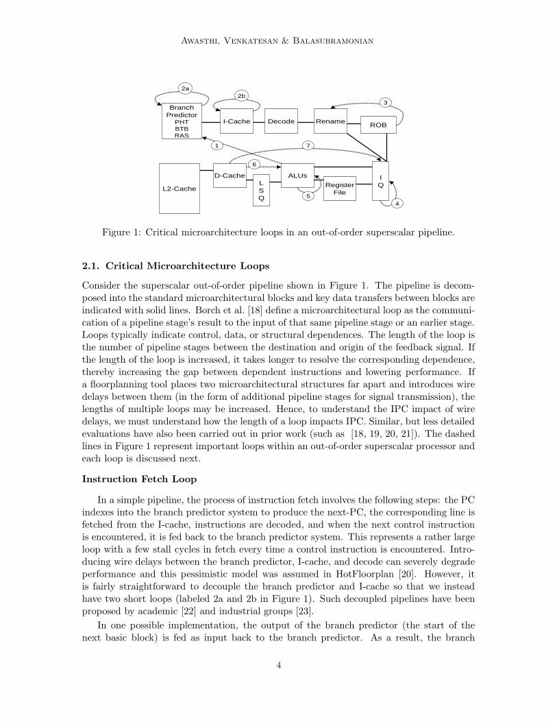
Figure 1: Critical microarchitecture loops in an out-of-order superscalar pipeline.
2.1. Critical Microarchitecture Loops
Consider the superscalar out-of-order pipeline shown in Figure 1. The pipeline is decom-posed into the standard microarchitectural blocks and key data transfers between blocks areindicated with solid lines. Borch et al. [18] define a microarchitectural loop as the communi-cation of a pipeline stage’s result to the input of that same pipeline stage or an earlier stage.Loops typically indicate control, data, or structural dependences. The length of the loop isthe number of pipeline stages between the destination and origin of the feedback signal. Ifthe length of the loop is increased, it takes longer to resolve the corresponding dependence,thereby increasing the gap between dependent instructions and lowering performance. Ifa floorplanning tool places two microarchitectural structures far apart and introduces wiredelays between them (in the form of additional pipeline stages for signal transmission), thelengths of multiple loops may be increased. Hence, to understand the IPC impact of wiredelays, we must understand how the length of a loop impacts IPC. Similar, but less detailedevaluations have also been carried out in prior work (such as [18, 19, 20, 21]). The dashedlines in Figure 1 represent important loops within an out-of-order superscalar processor andeach loop is discussed next.
Instruction Fetch Loop
In a simple pipeline, the process of instruction fetch involves the following steps: the PCindexes into the branch predictor system to produce the next-PC, the corresponding line isfetched from the I-cache, instructions are decoded, and when the next control instructionis encountered, it is fed back to the branch predictor system. This represents a rather largeloop with a few stall cycles in fetch every time a control instruction is encountered. Intro-ducing wire delays between the branch predictor, I-cache, and decode can severely degradeperformance and this pessimistic model was assumed in HotFloorplan [20]. However, itis fairly straightforward to decouple the branch predictor and I-cache so that we insteadhave two short loops (labeled 2a and 2b in Figure 1). Such decoupled pipelines have beenproposed by academic [22] and industrial groups [23].
In one possible implementation, the output of the branch predictor (the start of thenext basic block) is fed as input back to the branch predictor. As a result, the branch
4
Understanding the Impact of 3D Stacked Layouts on ILP
predictor system is now indexed with the PC that starts the basic block, not the PCthat terminates the basic block. This allows the branch predictor to produce basic blockstart PCs independent of the rest of the front-end. Our results show that this changein the branch predictor algorithm has a minimal impact on its accuracy. The front-endpipeline now consists of two major tight loops: the branch predictor loop (2a) and theI-cache loop (2b). The front-end is also part of the branch mis-predict resolution loop(1), which feeds from the ALU stage all the way back to the front-end. Thus, the primaryimpact of introducing a wire delay between front-end pipeline stages is an increase in branchmispredict penalty. Our relative results will hold true even if a different front-end pipelineimplementation (such as the next-line-and-set predictor in the Alpha 21264 I-cache [23]) isadopted, as long as the critical loops are short. Prior studies [24, 25, 20] have over-statedthe IPC impact of this wire delay because the branch predictor and I-cache were assumedto not be de-coupled.
Rename Loops
The introduction of wire delays either between the decode and rename stages or betweenthe rename and issue queue stages lengthens the penalty for a branch mispredict (loop 1).Since registers are allocated during rename, wire delays between the rename stage and theissue queue increase the duration that a register entry remains allocated (loop 3). Thisincreases the pressure on the register file and leads to smaller in-flight instruction windows.
Wakeup and Bypass Loops
There is a common mis-conception that wire delays between the issue queue and ALUslead to stall cycles between dependent instructions [24, 20]. This is not true because thepipeline can be easily decomposed into two tight loops – one for wakeup (loop 4) and onefor bypass (loop 5). When an instruction is selected for issue in cycle N , it first fetchesoperands from the register file, potentially traverses long wires, and then reaches the ALU.Because of these delays, the instruction may not begin execution at the ALU until the startof cycle N + D. If the ALU operation takes a single cycle, the result is bypassed to theinputs of the ALU so that a dependent instruction can execute on that ALU as early asthe start of cycle N + D + 1. For this to happen, the dependent instruction must leavethe issue queue in cycle N + 1. Therefore, as soon as the first instruction leaves the issuequeue, its output register tag is broadcast to the issue queue so that dependents can leavethe issue queue in the next cycle. Thus, operations within the issue queue must only beaware of the ALU latency, and not the time it takes for the instruction to reach the ALU(delay D). The gap between dependent instructions is therefore not determined by delayD, but by the time taken for the wakeup loop and by the time taken for the bypass loop(both of these loops were assumed to be 1 cycle in the above example). The introductionof wire delays between the issue queue and ALU because of floorplanning will not impacteither of these loops.
However, wire delays between the issue queue and ALU will impact another criticalloop that (to the best of our knowledge) has been dis-regarded by every floorplanningtool to date. This is the load hit speculation loop (loop 7 in Figure 1). The issue queueschedules dependent instructions based on the expected latency of the producing instruction.In modern processors, such as the Pentium4 [17], the issue queue optimistically assumes
5
Awasthi, Venkatesan & Balasubramonian
that the load will hit in the L1 data cache and accordingly schedules dependents. If theload latency is any more than this minimum latency, dependent instructions that havealready left the issue queue are squashed and subsequently re-played. To facilitate thisre-play, instructions can be kept in the issue queue until the load latency is known. Thus,load-hit speculation negatively impacts performance in two ways: (i) re-played instructionscontend twice for resources, (ii) issue queue occupancy increases, thereby supporting asmaller instruction window, on average. If any wire delays are introduced in the pipelinebetween the issue queue and ALU, or between the ALU and data cache, it takes longerto determine if a load is a hit or a miss. Correspondingly, the penalties for correct andincorrect load-hit speculations increase. We also model the Tornado effect [26], where anentire chain of instructions dependent on the load are issued, squashed, and re-played on aload miss.
Delays between the issue queue and ALUs also impact branch mispredict penalty andregister occupancy. They also increase the L1 miss penalty as it takes longer to re-start thepipeline after an L1 miss.
Bypassing Loops Between Groups of Functional Units
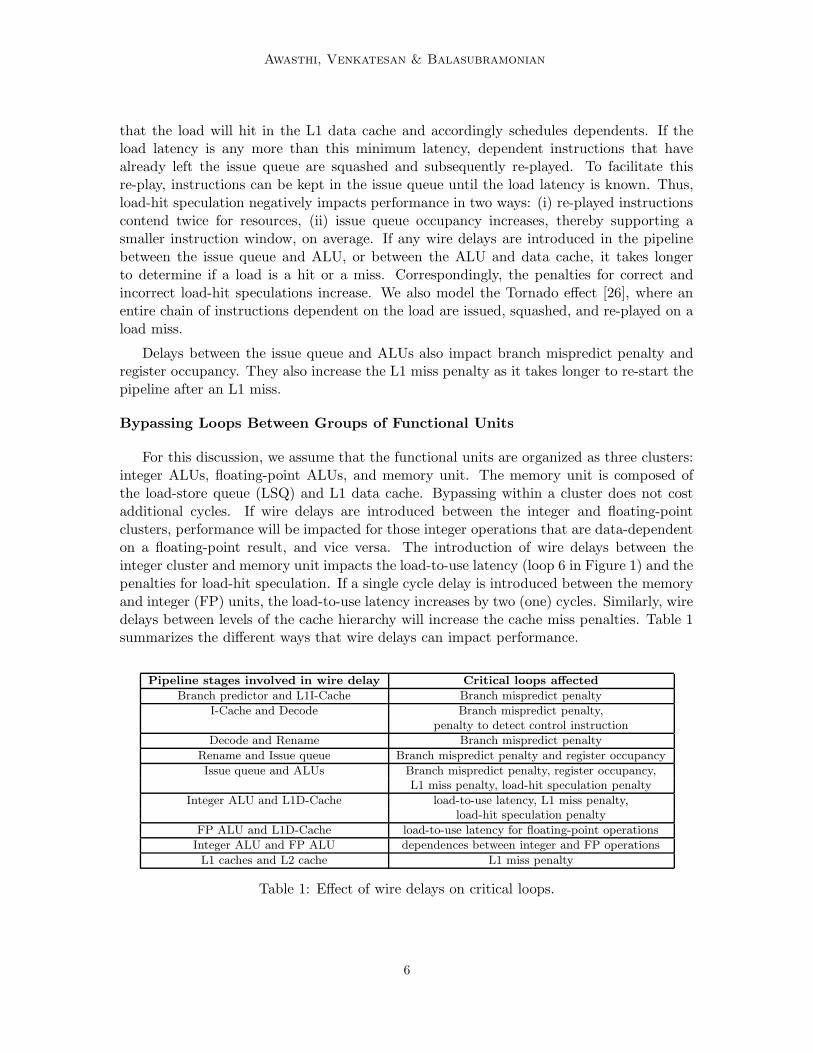
For this discussion, we assume that the functional units are organized as three clusters:integer ALUs, floating-point ALUs, and memory unit. The memory unit is composed ofthe load-store queue (LSQ) and L1 data cache. Bypassing within a cluster does not costadditional cycles. If wire delays are introduced between the integer and floating-pointclusters, performance will be impacted for those integer operations that are data-dependenton a floating-point result, and vice versa. The introduction of wire delays between theinteger cluster and memory unit impacts the load-to-use latency (loop 6 in Figure 1) and thepenalties for load-hit speculation. If a single cycle delay is introduced between the memoryand integer (FP) units, the load-to-use latency increases by two (one) cycles. Similarly, wiredelays between levels of the cache hierarchy will increase the cache miss penalties. Table 1summarizes the different ways that wire delays can impact performance.
Pipeline stages involved in wire delay Critical loops affected
Branch predictor and L1I-Cache Branch mispredict penalty
I-Cache and Decode Branch mispredict penalty,penalty to detect control instruction
Decode and Rename Branch mispredict penalty
Rename and Issue queue Branch mispredict penalty and register occupancy
Issue queue and ALUs Branch mispredict penalty, register occupancy,L1 miss penalty, load-hit speculation penalty
Integer ALU and L1D-Cache load-to-use latency, L1 miss penalty,load-hit speculation penalty
FP ALU and L1D-Cache load-to-use latency for floating-point operations
Integer ALU and FP ALU dependences between integer and FP operations
L1 caches and L2 cache L1 miss penalty
Table 1: Effect of wire delays on critical loops.
6
Understanding the Impact of 3D Stacked Layouts on ILP
2.2. Floorplanning Algorithms
Floorplanning algorithms [19, 27, 28, 20] typically employ a simulated annealing process toevaluate a wide range of candidate floorplans. The objective functions for these algorithmsattempt to minimize some combination of silicon/metal area, wire power, and chip temper-ature. In modern microprocessors, since delays across global wires can exceed a single cycle,a floorplanning tool must also consider the performance impact of introducing multi-cyclewire delays between two communicating microarchitectural blocks. The objective functionin a state-of-the-art floorplanner can be represented as follows [19, 27, 28, 20] :
λA×Area metric + λT×Temperature+∑
ij
λW×Wij×Activityij +∑
ij
λI×dij×IPC penaltyij
In the equation above, λA, λT , λW , and λI represent constants that tune the relativeimportance of each metric (area, temperature, wire power, and IPC), Wij represents themetal area (length × number of wires) between microarchitectural blocks i and j, Activityij
captures the switching activity for the wires between blocks i and j, the metric dij repre-sents the distance between blocks i and j in terms of cycles, while IPC penaltyij is theperformance penalty when a single cycle delay is introduced between blocks i and j. Themetrics Wij , dij , Temperature, and Area metric are computed for every floorplan beingconsidered, while metrics Activityij and IPC penaltyij are computed once with an archi-tectural simulator and fed as inputs to the floorplanner. The design of efficient floorplannersremains an open problem and many variations to the above objective function can be foundin the literature. This work does not propose a novel floorplanning algorithm or objectivefunction. We are using an existing floorplanning algorithm to automate the task of findinga layout that minimizes critical wire lengths. In the next section, we accurately character-ize the IPC penalty term with detailed models for the critical loops just described. Thefloorplanning tool takes in this input to derive 2D and 3D floorplans that (among otherthings) reduce the IPC penalty of wire delays.
3. The Impact of Wire Delays on Floorplanning Algorithms
3.1. Methodology
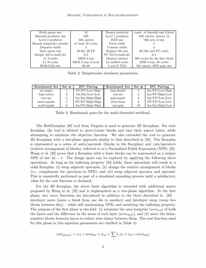
The simulator used in this study is based on Simplescalar-3.0 [29], a cycle-accurate simulatorfor the Alpha AXP architecture. It is extended to not only model multiple threads andseparate issue queues, register files, and reorder buffer, but also the microarchitecturalloops and features discussed in Section 2.1.. The single-thread benchmark suite includes 23SPEC-2k programs, executed for 100 million instruction windows identified by the Simpointtool [30]. The processor parameters for the base configuration are listed in Table 2. Wealso repeat our experiments for a core that supports the execution of two threads in SMTfashion. The SMT core has the same parameters as the single-thread processor described inTable 2, except that register file and ROB resources are doubled. Our SMT model employsthe ICOUNT [31] fetch policy and all resources (except the ROB) are dynamically shared bythe two threads. For the multi-threaded workload, we form a benchmark set that consistsof 10 different pairs of programs. Programs are paired to generate a good mix of high IPC,low IPC, FP, and Integer workloads. Table 3 shows our benchmark pairs. Multithreadedworkloads are executed until the first thread commits 100 million instructions.
7
Awasthi, Venkatesan & Balasubramonian
Fetch queue size 16 Branch predictor comb. of bimodal and 2-levelBimodal predictor size 16K Level 1 predictor 16K entries, history 12
Level 2 predictor 16K entries BTB size 16K sets, 2-wayBranch mispredict penalty at least 10 cycles Fetch width 4
Dispatch width 4 Commit width 4Issue queue size 20 Int, 20 FP Register file size 80 (Int and FP, each)
Integer ALUs/mult-div 4/2 FP ALUs/mult-div 2/1L1 I-cache 32KB 2-way Memory latency 300 cycles for the first blockL1 D-cache 32KB 2-way 2-cycle L2 unified cache 2MB 8-way, 30 cycles
ROB/LSQ size 80/40 I and D TLB 128 entries, 8KB page size
Table 2: Simplescalar simulator parameters.
Benchmark Set Set # IPC Pairing Benchmark Set Set # IPC Pairing
art-applu 1 FP/FP/Low/High bzip-fma3d 2 Int/FP/Low/Highbzip-vortex 3 Int/Int/Low/Low eon-art 4 Int/FP/High/Low
eon-vpr 5 Int/Int/High/High gzip-mgrid 6 Int/FP/Low/Lowmesa-equake 7 FP/FP/High/High swim-lucas 8 FP/FP/Low/Lowtwolf-equake 9 Int/FP/High/High vpr-gzip 10 Int/Int/High/Low
Table 3: Benchmark pairs for the multi-threaded workload.
The HotFloorplan [20] tool from Virginia is used to generate 2D floorplans. For eachfloorplan, the tool is allowed to move/rotate blocks and vary their aspect ratios, whileattempting to minimize the objective function. We also extended the tool to generate3D floorplans with a two-phase approach similar to that described in [32]. The floorplanis represented as a series of units/operands (blocks in the floorplan) and cuts/operators(relative arrangement of blocks), referred to as a Normalized Polish Expression (NPE) [33].Wong et al. [33] prove that a floorplan with n basic blocks can be represented as a uniqueNPE of size 2n − 1. The design space can be explored by applying the following threeoperations. As long as the balloting property [33] holds, these operations will result in avalid floorplan: (i) swap adjacent operands, (ii) change the relative arrangement of blocks(i.e., complement the operators in NPE), and (iii) swap adjacent operator and operand.This is repeatedly performed as part of a simulated annealing process until a satisfactoryvalue for the cost function is obtained.
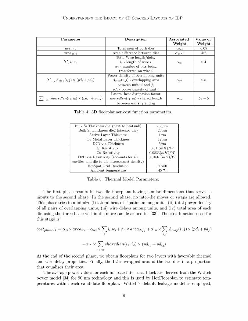
For the 3D floorplan, the above basic algorithm is extended with additional movesproposed by Hung et al. [32] and is implemented as a two-phase algorithm. In the firstphase, two move functions are introduced in addition to the three described in [33] –interlayer move (move a block from one die to another) and interlayer swap (swap twoblocks between dies) – while still maintaining NPEs and satisfying the balloting property.The purpose of the first phase is two-fold: (i) minimize the area footprint (areatot) of boththe layers and the difference in the areas of each layer (areadiff ), and (ii) move the delay-sensitive blocks between layers to reduce wire delays between them. The cost function usedfor this phase is (the equation parameters are clarified in Table 4):
costphaseI = αA × areatot + αwl ×
∑
i
li.wi + αd × areadiff
8
Understanding the Impact of 3D Stacked Layouts on ILP
Parameter Description Associated Value of
Weight Weight
areatot Total area of both dies αtot 0.05
areadiff Area difference between dies αdiff 4e5
Total Wire length/delay∑ili.wi li - length of wire i αwl 0.4
wi - number of bits beingtransferred on wire i
Power density of overlapping units∑i,j
Aolap(i, j) × (pdi + pdj) Aolap(i, j) - overlapping area αvh 0.5
between units i and j,pdi - power density of unit i
Lateral heat dissipation factor∑i1,i2
sharedlen(i1, i2) × (pdi1 + pdi2) sharedlen(i1, i2) - shared length αlh 5e − 5
between units i1 and i2
Table 4: 3D floorplanner cost function parameters.
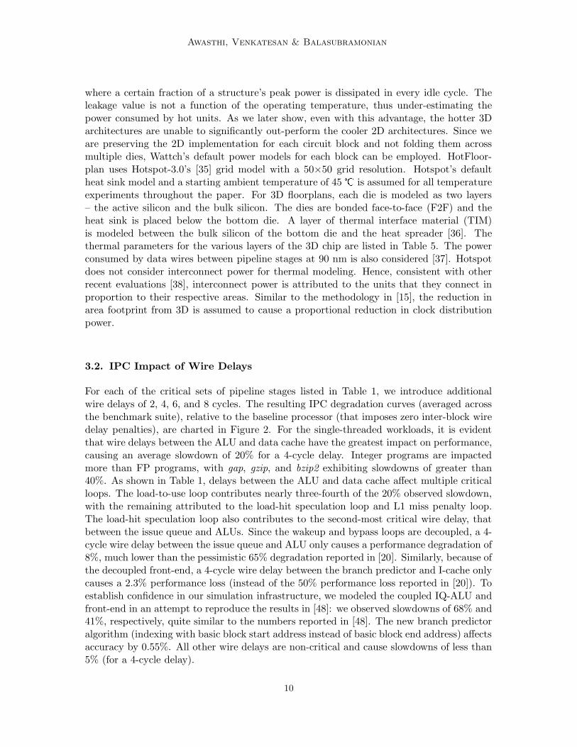
Bulk Si Thickness die1(next to heatsink) 750µmBulk Si Thickness die2 (stacked die) 20µm
Active Layer Thickness 1µmCu Metal Layer Thickness 12µm
D2D via Thickness 5µmSi Resistivity 0.01 (mK)/WCu Resistivity 0.0833(mK)/W
D2D via Resistivity (accounts for air 0.0166 (mK)/Wcavities and die to die interconnect density)
HotSpot Grid Resolution 50x50Ambient temperature 45
�
Table 5: Thermal Model Parameters.
The first phase results in two die floorplans having similar dimensions that serve asinputs to the second phase. In the second phase, no inter-die moves or swaps are allowed.This phase tries to minimize (i) lateral heat dissipation among units, (ii) total power densityof all pairs of overlapping units, (iii) wire delays among units, and (iv) total area of eachdie using the three basic within-die moves as described in [33]. The cost function used forthis stage is:
costphaseII = αA×areatot +αwl×
∑
i
li.wi +αd×areadiff +αvh×
∑
i,j
Aolap(i, j)×(pdi +pdj)
+αlh ×
∑
i1,i2
sharedlen(i1, i2) × (pdi1 + pdi2)
At the end of the second phase, we obtain floorplans for two layers with favorable thermaland wire-delay properties. Finally, the L2 is wrapped around the two dies in a proportionthat equalizes their area.
The average power values for each microarchitectural block are derived from the Wattchpower model [34] for 90 nm technology and this is used by HotFloorplan to estimate tem-peratures within each candidate floorplan. Wattch’s default leakage model is employed,
9
Awasthi, Venkatesan & Balasubramonian
where a certain fraction of a structure’s peak power is dissipated in every idle cycle. Theleakage value is not a function of the operating temperature, thus under-estimating thepower consumed by hot units. As we later show, even with this advantage, the hotter 3Darchitectures are unable to significantly out-perform the cooler 2D architectures. Since weare preserving the 2D implementation for each circuit block and not folding them acrossmultiple dies, Wattch’s default power models for each block can be employed. HotFloor-plan uses Hotspot-3.0’s [35] grid model with a 50×50 grid resolution. Hotspot’s defaultheat sink model and a starting ambient temperature of 45 � is assumed for all temperatureexperiments throughout the paper. For 3D floorplans, each die is modeled as two layers– the active silicon and the bulk silicon. The dies are bonded face-to-face (F2F) and theheat sink is placed below the bottom die. A layer of thermal interface material (TIM)is modeled between the bulk silicon of the bottom die and the heat spreader [36]. Thethermal parameters for the various layers of the 3D chip are listed in Table 5. The powerconsumed by data wires between pipeline stages at 90 nm is also considered [37]. Hotspotdoes not consider interconnect power for thermal modeling. Hence, consistent with otherrecent evaluations [38], interconnect power is attributed to the units that they connect inproportion to their respective areas. Similar to the methodology in [15], the reduction inarea footprint from 3D is assumed to cause a proportional reduction in clock distributionpower.
3.2. IPC Impact of Wire Delays
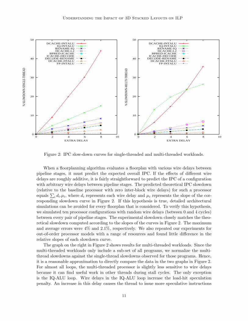
For each of the critical sets of pipeline stages listed in Table 1, we introduce additionalwire delays of 2, 4, 6, and 8 cycles. The resulting IPC degradation curves (averaged acrossthe benchmark suite), relative to the baseline processor (that imposes zero inter-block wiredelay penalties), are charted in Figure 2. For the single-threaded workloads, it is evidentthat wire delays between the ALU and data cache have the greatest impact on performance,causing an average slowdown of 20% for a 4-cycle delay. Integer programs are impactedmore than FP programs, with gap, gzip, and bzip2 exhibiting slowdowns of greater than40%. As shown in Table 1, delays between the ALU and data cache affect multiple criticalloops. The load-to-use loop contributes nearly three-fourth of the 20% observed slowdown,with the remaining attributed to the load-hit speculation loop and L1 miss penalty loop.The load-hit speculation loop also contributes to the second-most critical wire delay, thatbetween the issue queue and ALUs. Since the wakeup and bypass loops are decoupled, a 4-cycle wire delay between the issue queue and ALU only causes a performance degradation of8%, much lower than the pessimistic 65% degradation reported in [20]. Similarly, because ofthe decoupled front-end, a 4-cycle wire delay between the branch predictor and I-cache onlycauses a 2.3% performance loss (instead of the 50% performance loss reported in [20]). Toestablish confidence in our simulation infrastructure, we modeled the coupled IQ-ALU andfront-end in an attempt to reproduce the results in [48]: we observed slowdowns of 68% and41%, respectively, quite similar to the numbers reported in [48]. The new branch predictoralgorithm (indexing with basic block start address instead of basic block end address) affectsaccuracy by 0.55%. All other wire delays are non-critical and cause slowdowns of less than5% (for a 4-cycle delay).
10
Understanding the Impact of 3D Stacked Layouts on ILP
0
10
20
30
40
50
0 2 4 6 8 10
% S
LOW
DOW
N-SI
NGLE
-THR
EAD
EXTRA DELAY
DCACHE-INTALUIQ-INTALU
RENAME-IQDCACHE-L2
BPRED-ICACHEICACHE-DECODE
DECODE-RENAMEDCACHE-FPALU
FP-INTALU
0
10
20
30
40
50
0 2 4 6 8 10
% S
LOW
DOW
N-M
ULTI
-THR
EAD
EXTRA DELAY
DCACHE-INTALUIQ-INTALU
RENAME-IQDCACHE-L2
BPRED-ICACHEICACHE-DECODE
DECODE-RENAMEDCACHE-FPALU
FP-INTALU
Figure 2: IPC slow-down curves for single-threaded and multi-threaded workloads.
When a floorplanning algorithm evaluates a floorplan with various wire delays betweenpipeline stages, it must predict the expected overall IPC. If the effects of different wiredelays are roughly additive, it is fairly straightforward to predict the IPC of a configurationwith arbitrary wire delays between pipeline stages. The predicted theoretical IPC slowdown(relative to the baseline processor with zero inter-block wire delays) for such a processorequals
∑i di.µi, where di represents each wire delay and µi represents the slope of the cor-
responding slowdown curve in Figure 2. If this hypothesis is true, detailed architecturalsimulations can be avoided for every floorplan that is considered. To verify this hypothesis,we simulated ten processor configurations with random wire delays (between 0 and 4 cycles)between every pair of pipeline stages. The experimental slowdown closely matches the theo-retical slowdown computed according to the slopes of the curves in Figure 2. The maximumand average errors were 4% and 2.1%, respectively. We also repeated our experiments forout-of-order processor models with a range of resources and found little difference in therelative slopes of each slowdown curve.
The graph on the right in Figure 2 shows results for multi-threaded workloads. Since themulti-threaded workloads only include a sub-set of all programs, we normalize the multi-thread slowdowns against the single-thread slowdowns observed for those programs. Hence,it is a reasonable approximation to directly compare the data in the two graphs in Figure 2.For almost all loops, the multi-threaded processor is slightly less sensitive to wire delaysbecause it can find useful work in other threads during stall cycles. The only exceptionis the IQ-ALU loop. Wire delays in the IQ-ALU loop increase the load-hit speculationpenalty. An increase in this delay causes the thread to issue more speculative instructions
11
Awasthi, Venkatesan & Balasubramonian
– hence wire delays are an impediment to the execution of the co-scheduled thread, not anopportunity to steal idle slots. Further, as this wire delay increases, issue queue occupancyincreases and since this is a shared resource, it further inhibits the co-scheduled thread. Wehave verified that the multi-threaded results do not influence our 2D/3D floorplans greatly,so the rest of the paper only discusses single-thread workloads.
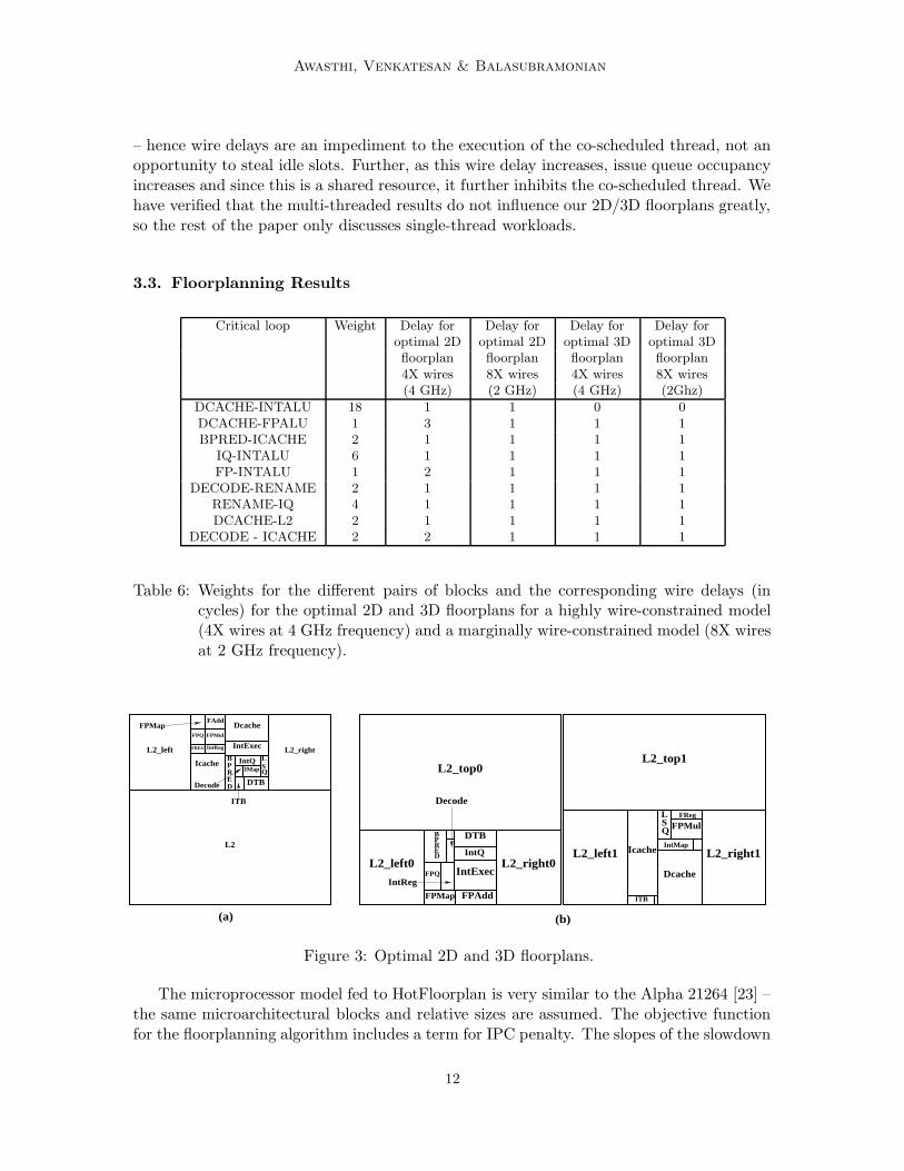
3.3. Floorplanning Results
Critical loop Weight Delay for Delay for Delay for Delay foroptimal 2D optimal 2D optimal 3D optimal 3Dfloorplan floorplan floorplan floorplan4X wires 8X wires 4X wires 8X wires(4 GHz) (2 GHz) (4 GHz) (2Ghz)
DCACHE-INTALU 18 1 1 0 0DCACHE-FPALU 1 3 1 1 1BPRED-ICACHE 2 1 1 1 1
IQ-INTALU 6 1 1 1 1FP-INTALU 1 2 1 1 1
DECODE-RENAME 2 1 1 1 1RENAME-IQ 4 1 1 1 1DCACHE-L2 2 1 1 1 1
DECODE - ICACHE 2 2 1 1 1
Table 6: Weights for the different pairs of blocks and the corresponding wire delays (incycles) for the optimal 2D and 3D floorplans for a highly wire-constrained model(4X wires at 4 GHz frequency) and a marginally wire-constrained model (8X wiresat 2 GHz frequency).
QS
BPRED
BPRED
LSQ
FAdd
(a) (b)
IcacheL2_left1 L2_right1
ITB
Dcache
IntMap
FPMulFRegL
L2_top1
L2_left0 L2_right0
FPAdd
IntExec
DTB
FPMap
IntQ
FPQ
Decode
IntReg
L2_top0
Dcache
IntExec
L2
L2_rightL2_left
Icache
Decode DTB
IntQIMap
FPMul
IntReg
FPQ
FREG
ITB
FPMap
Figure 3: Optimal 2D and 3D floorplans.
The microprocessor model fed to HotFloorplan is very similar to the Alpha 21264 [23] –the same microarchitectural blocks and relative sizes are assumed. The objective functionfor the floorplanning algorithm includes a term for IPC penalty. The slopes of the slowdown
12
Understanding the Impact of 3D Stacked Layouts on ILP
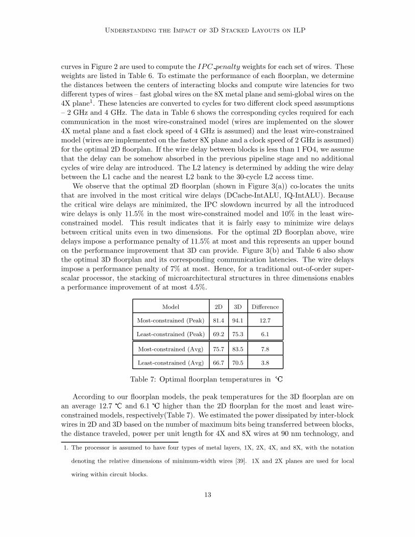
curves in Figure 2 are used to compute the IPC penalty weights for each set of wires. Theseweights are listed in Table 6. To estimate the performance of each floorplan, we determinethe distances between the centers of interacting blocks and compute wire latencies for twodifferent types of wires – fast global wires on the 8X metal plane and semi-global wires on the4X plane1. These latencies are converted to cycles for two different clock speed assumptions– 2 GHz and 4 GHz. The data in Table 6 shows the corresponding cycles required for eachcommunication in the most wire-constrained model (wires are implemented on the slower4X metal plane and a fast clock speed of 4 GHz is assumed) and the least wire-constrainedmodel (wires are implemented on the faster 8X plane and a clock speed of 2 GHz is assumed)for the optimal 2D floorplan. If the wire delay between blocks is less than 1 FO4, we assumethat the delay can be somehow absorbed in the previous pipeline stage and no additionalcycles of wire delay are introduced. The L2 latency is determined by adding the wire delaybetween the L1 cache and the nearest L2 bank to the 30-cycle L2 access time.
We observe that the optimal 2D floorplan (shown in Figure 3(a)) co-locates the unitsthat are involved in the most critical wire delays (DCache-IntALU, IQ-IntALU). Becausethe critical wire delays are minimized, the IPC slowdown incurred by all the introducedwire delays is only 11.5% in the most wire-constrained model and 10% in the least wire-constrained model. This result indicates that it is fairly easy to minimize wire delaysbetween critical units even in two dimensions. For the optimal 2D floorplan above, wiredelays impose a performance penalty of 11.5% at most and this represents an upper boundon the performance improvement that 3D can provide. Figure 3(b) and Table 6 also showthe optimal 3D floorplan and its corresponding communication latencies. The wire delaysimpose a performance penalty of 7% at most. Hence, for a traditional out-of-order super-scalar processor, the stacking of microarchitectural structures in three dimensions enablesa performance improvement of at most 4.5%.
Model 2D 3D Difference
Most-constrained (Peak) 81.4 94.1 12.7
Least-constrained (Peak) 69.2 75.3 6.1
Most-constrained (Avg) 75.7 83.5 7.8
Least-constrained (Avg) 66.7 70.5 3.8
Table 7: Optimal floorplan temperatures in �
According to our floorplan models, the peak temperatures for the 3D floorplan are onan average 12.7 � and 6.1 � higher than the 2D floorplan for the most and least wire-constrained models, respectively(Table 7). We estimated the power dissipated by inter-blockwires in 2D and 3D based on the number of maximum bits being transferred between blocks,the distance traveled, power per unit length for 4X and 8X wires at 90 nm technology, and
1. The processor is assumed to have four types of metal layers, 1X, 2X, 4X, and 8X, with the notation
denoting the relative dimensions of minimum-width wires [39]. 1X and 2X planes are used for local
wiring within circuit blocks.
13
Awasthi, Venkatesan & Balasubramonian
an activity factor of 0.5. In addition to the 50% reduction in clock distribution power, weobserved a 39% reduction in power for inter-block communication. We acknowledge that itis difficult to capture inter-block control signals in such a quantification, so this is a roughestimate at best.
Our primary conclusion from the first half of the paper is that the potential for perfor-mance improvement with the stacking approach is marginal for simple superscalar cores.However, the associated design/complexity cost is low and energy per instruction is reduced.
Our conclusions differ from those drawn in the study by Black et al. [6]. That studyreports a 15% performance improvement by implementing a Pentium4 core in 3D. Thisdifference can be attributed to two sources: (i) The Pentium4 2D layout places the SIMDunit between the FP register file and FP ALUs. This introduces a 1-cycle delay betweenthe FP register file and FP ALUs, modeled as a 2-cycle increase in the latency of all FPinstructions. The move to 3D eliminates this wire delay and improves performance by 4%.If the latency of all FP instructions is reduced by 2 cycles in our simulation infrastructure,we too observe a similar 3% performance improvement (for the SPEC2k FP benchmarks).However, this aspect is left out of the results shown above. Firstly, as explained in Section2.1, a delay between the register file and ALU should not introduce stall cycles betweendependent instructions if full bypassing is provided. Secondly, the FP ALUs and FP registerfile are in close proximity in our 2D layout. These observations do highlight the point thata 2D industrial implementation may have some inefficiencies (for example, inability toprovide full bypassing or inability to co-locate certain structures) that can be elided witha 3D layout. (ii) The Pentium4 has a small store queue and is sensitive to post-retirementpipeline stages involving the store instruction. By eliminating post-retirement wire delayand releasing the store queue entry sooner, a 3% performance improvement is reported in[6]. In our simulation environment, if we implement a 14-entry store queue and release anentry 30 cycles after the store retires, we observe a 3% improvement if the post-retirementdelay is reduced by 30%. This phenomenon disappears if the store queue size is eliminatedas a bottleneck (by increasing its size to at least 24). We assume that the store queue sizewill not be a bottleneck and exclude this aspect from our simulation results. Our studyis more pessimistic about the potential of 3D because our pipeline model has balancedresources, is simpler and shorter (perhaps more indicative of future cores), and takes a rosyview of the efficiency of a 2D layout.
4. 3D Layouts for Clustered Architectures
The high-level insight drawn from the previous section can be summarized as follows: (i)delays between the integer ALUs and data cache are critical and must be minimized, and (ii)it is fairly straightforward to minimize these delays in traditional 2D superscalar processors.While 3D-stacking may offer little benefit for such processors, it may hold more promise forILP in an aggressive superscalar with many resources. A clustered architecture is an exampleof a single-thread2 complexity-effective processor implementation that leverages a number
2. Clustered architectures can be multi-threaded [40, 41, 42] and are attractive as they are capable of high
clock speeds, high ILP, and high thread-level parallelism.
14
Understanding the Impact of 3D Stacked Layouts on ILP
of distributed resources for high ILP [43, 44, 45, 42, 46]. Since clustered architecturesincorporate multiple distributed ALUs and data cache banks, they are more limited by wiredelays and likely to benefit from 3D. The rest of the paper quantifies the potential of 3D fora specific dynamically scheduled implementation of a clustered architecture, although, weexpect the gathered insight to also apply to other partitioned architecture implementations.
4.1. Baseline Clustered Architecture
Many prior papers (such as [43, 44, 45, 47, 42, 46]) have shown that a clustered microar-chitecture is a complexity-effective implementation of a high-ILP processor capable of sup-porting a large window of in-flight instructions. The Alpha 21264 is a commercial exampleof such a design, where integer execution resources are partitioned across two clusters [23].
The clustered architecture employs small computation units (clusters) that can be easilyreplicated on the die. An interconnect fabric enables communication between clusters.Each cluster consists of a small issue queue, physical register file, and a limited number offunctional units with a single cycle bypass network among them. Dependence chains canexecute quickly if they only access values within a cluster. The small sizes of structureswithin each cluster enable high clock speed and low design complexity.
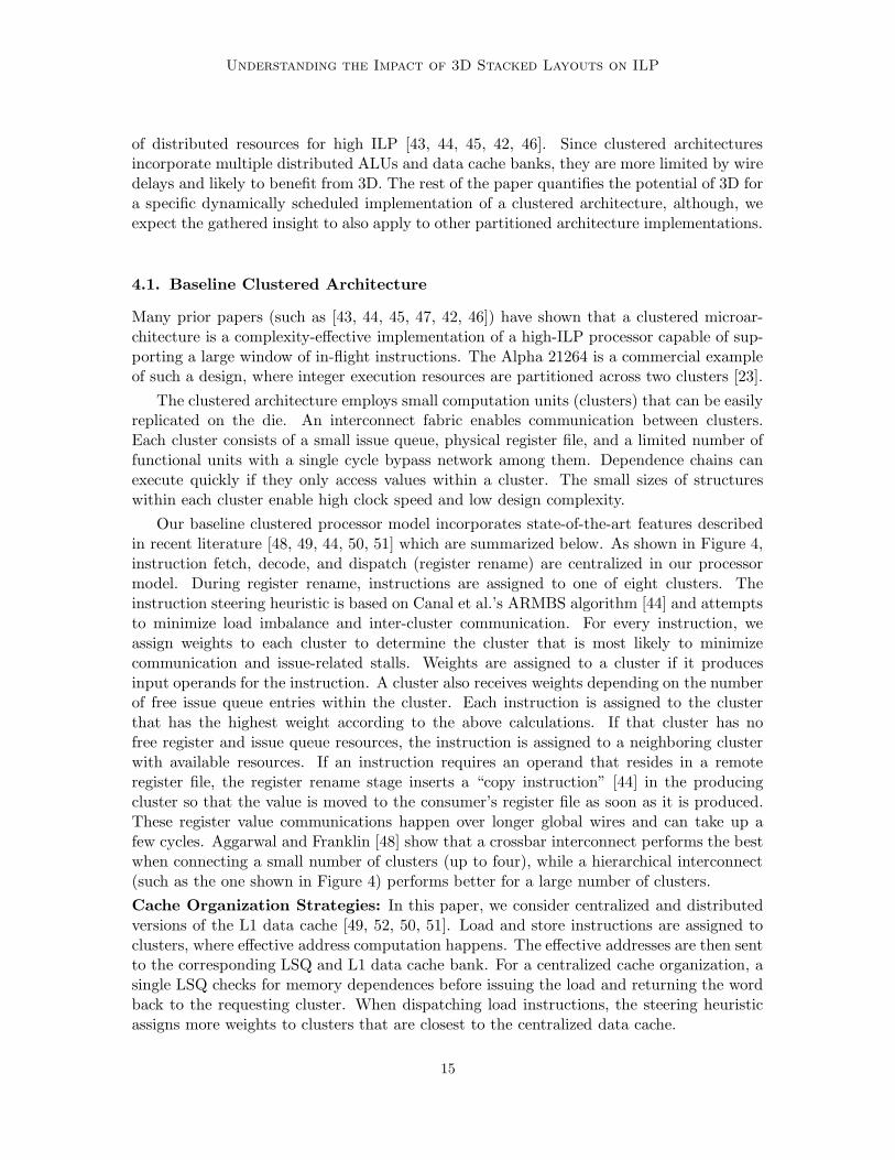
Our baseline clustered processor model incorporates state-of-the-art features describedin recent literature [48, 49, 44, 50, 51] which are summarized below. As shown in Figure 4,instruction fetch, decode, and dispatch (register rename) are centralized in our processormodel. During register rename, instructions are assigned to one of eight clusters. Theinstruction steering heuristic is based on Canal et al.’s ARMBS algorithm [44] and attemptsto minimize load imbalance and inter-cluster communication. For every instruction, weassign weights to each cluster to determine the cluster that is most likely to minimizecommunication and issue-related stalls. Weights are assigned to a cluster if it producesinput operands for the instruction. A cluster also receives weights depending on the numberof free issue queue entries within the cluster. Each instruction is assigned to the clusterthat has the highest weight according to the above calculations. If that cluster has nofree register and issue queue resources, the instruction is assigned to a neighboring clusterwith available resources. If an instruction requires an operand that resides in a remoteregister file, the register rename stage inserts a “copy instruction” [44] in the producingcluster so that the value is moved to the consumer’s register file as soon as it is produced.These register value communications happen over longer global wires and can take up afew cycles. Aggarwal and Franklin [48] show that a crossbar interconnect performs the bestwhen connecting a small number of clusters (up to four), while a hierarchical interconnect(such as the one shown in Figure 4) performs better for a large number of clusters.
Cache Organization Strategies: In this paper, we consider centralized and distributedversions of the L1 data cache [49, 52, 50, 51]. Load and store instructions are assigned toclusters, where effective address computation happens. The effective addresses are then sentto the corresponding LSQ and L1 data cache bank. For a centralized cache organization, asingle LSQ checks for memory dependences before issuing the load and returning the wordback to the requesting cluster. When dispatching load instructions, the steering heuristicassigns more weights to clusters that are closest to the centralized data cache.
15
Awasthi, Venkatesan & Balasubramonian
CentralizedFront-End
L1D cache bank 0 L1D cache bank 1
Figure 4: Baseline 2D implementation of the 8-cluster system.
Cluster
(a) Arch-1 (cache-on-cluster) (b) Arch-2 (cluster on cluster) (c) Arch-3 (staggered)
Cache bank Intra-die horizontal wire Inter-die vertical wire
Die 1
Die 0
Figure 5: Block diagrams for 3D organizations of the 8 cluster system.
As examples of decentralized cache organizations, we consider replicated and word-interleaved caches. In a replicated cache, each cache bank maintains a copy of the L1 datacache. This ensures that every cluster is relatively close to all of the data in the L1 cache.However, in addition to the high area overhead, every write and cache refill must now besent to every cache bank. An LSQ at every cache bank checks for memory dependencesbefore issuing loads. A word-interleaved cache distributes every cache line among the variouscache banks (for example, all odd words in one bank and even words in another bank). Thisensures that every cluster is relatively close to some of the data in the L1 cache. Word-interleaved caches have larger capacities than replicated caches for a fixed area budget. Oncethe effective address is computed, it is sent to the corresponding LSQ and cache bank. Loadinstructions must be steered to clusters that are in close proximity to the appropriate cachebank. Since the effective address is not known at dispatch time, a predictor is required.We experimented with various bank predictors and were unable to achieve an accuracyhigher than 70%. The instruction steering heuristic performs best if it dis-regards the bankprediction and attempts to optimize the other criteria. A mechanism [51] is required toensure that memory dependences are not violated. When a store is dispatched, each LSQ isassigned a dummy entry for that store, preventing subsequent loads from issuing. Once thestore address is known, it is communicated to the corresponding LSQ and the other LSQremoves the dummy entry. Thus, both decentralized caches suffer from the problem thatstores have to be broadcast to all LSQs.
16
Understanding the Impact of 3D Stacked Layouts on ILP
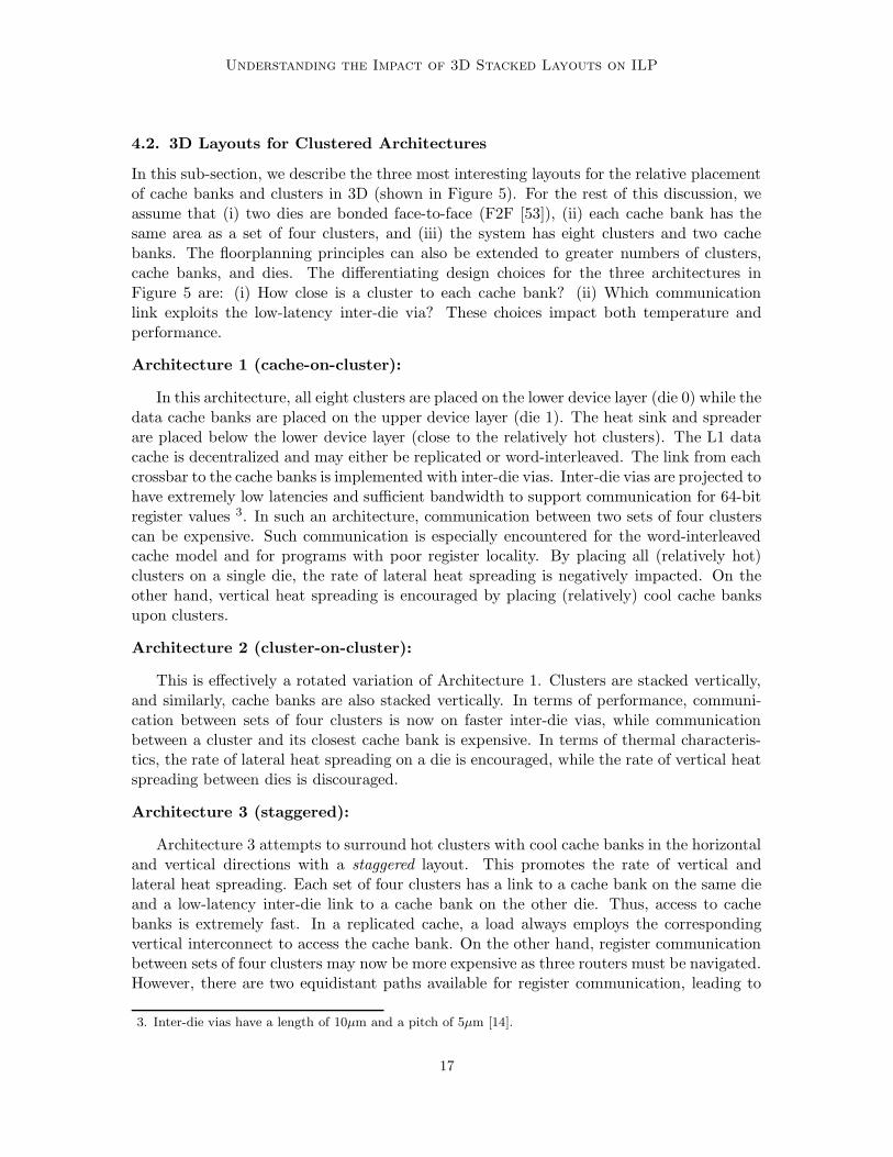
4.2. 3D Layouts for Clustered Architectures
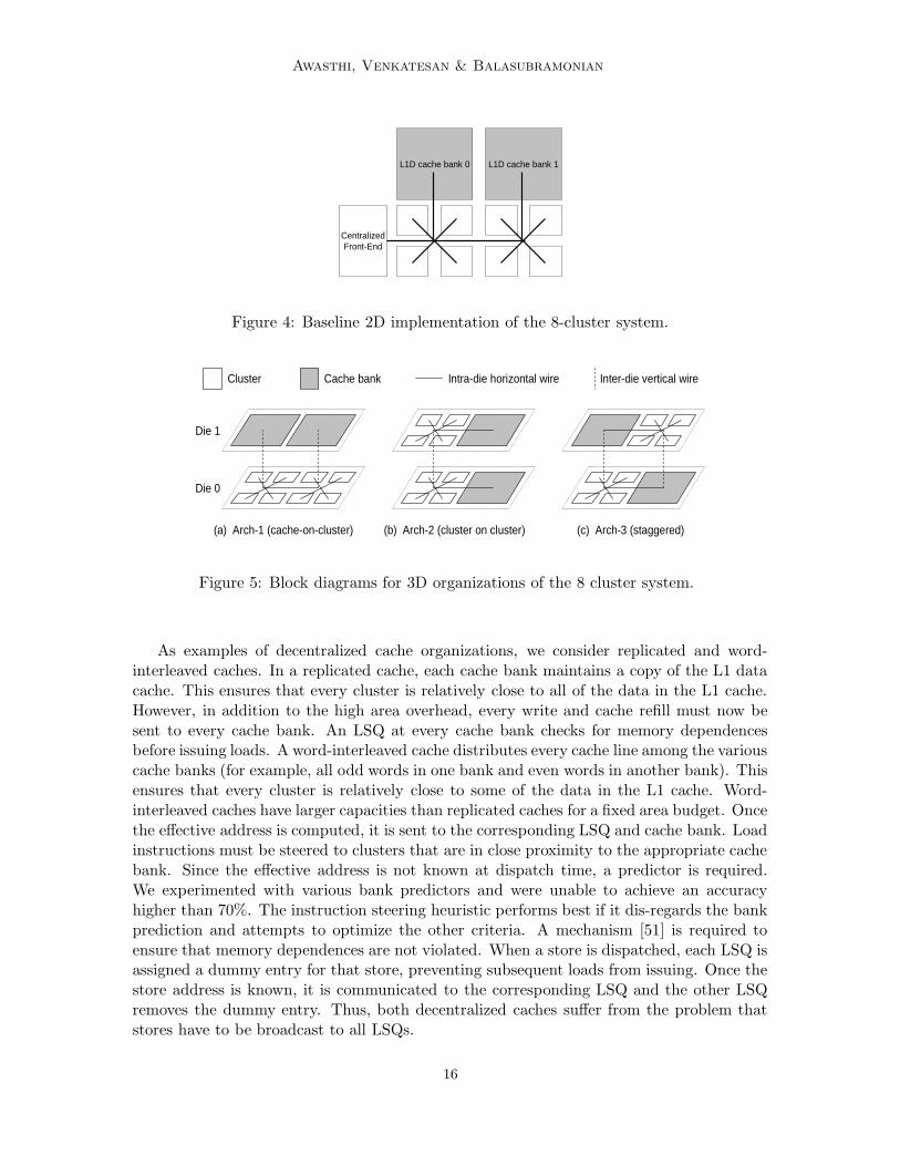
In this sub-section, we describe the three most interesting layouts for the relative placementof cache banks and clusters in 3D (shown in Figure 5). For the rest of this discussion, weassume that (i) two dies are bonded face-to-face (F2F [53]), (ii) each cache bank has thesame area as a set of four clusters, and (iii) the system has eight clusters and two cachebanks. The floorplanning principles can also be extended to greater numbers of clusters,cache banks, and dies. The differentiating design choices for the three architectures inFigure 5 are: (i) How close is a cluster to each cache bank? (ii) Which communicationlink exploits the low-latency inter-die via? These choices impact both temperature andperformance.
Architecture 1 (cache-on-cluster):
In this architecture, all eight clusters are placed on the lower device layer (die 0) while thedata cache banks are placed on the upper device layer (die 1). The heat sink and spreaderare placed below the lower device layer (close to the relatively hot clusters). The L1 datacache is decentralized and may either be replicated or word-interleaved. The link from eachcrossbar to the cache banks is implemented with inter-die vias. Inter-die vias are projected tohave extremely low latencies and sufficient bandwidth to support communication for 64-bitregister values 3. In such an architecture, communication between two sets of four clusterscan be expensive. Such communication is especially encountered for the word-interleavedcache model and for programs with poor register locality. By placing all (relatively hot)clusters on a single die, the rate of lateral heat spreading is negatively impacted. On theother hand, vertical heat spreading is encouraged by placing (relatively) cool cache banksupon clusters.
Architecture 2 (cluster-on-cluster):
This is effectively a rotated variation of Architecture 1. Clusters are stacked vertically,and similarly, cache banks are also stacked vertically. In terms of performance, communi-cation between sets of four clusters is now on faster inter-die vias, while communicationbetween a cluster and its closest cache bank is expensive. In terms of thermal characteris-tics, the rate of lateral heat spreading on a die is encouraged, while the rate of vertical heatspreading between dies is discouraged.
Architecture 3 (staggered):
Architecture 3 attempts to surround hot clusters with cool cache banks in the horizontaland vertical directions with a staggered layout. This promotes the rate of vertical andlateral heat spreading. Each set of four clusters has a link to a cache bank on the same dieand a low-latency inter-die link to a cache bank on the other die. Thus, access to cachebanks is extremely fast. In a replicated cache, a load always employs the correspondingvertical interconnect to access the cache bank. On the other hand, register communicationbetween sets of four clusters may now be more expensive as three routers must be navigated.However, there are two equidistant paths available for register communication, leading to
3. Inter-die vias have a length of 10µm and a pitch of 5µm [14].
17
Awasthi, Venkatesan & Balasubramonian
Cluster
(a) Arch-1 (cache-on-cluster) (b) Arch-2 (cluster on cluster) (c) Arch-3 (staggered)
Cache bank Intra-die horizontal wire Inter-die vertical wire
Die 1
Die 0
Figure 6: Block diagrams for 3D organizations of the 4 cluster system.
fewer contention cycles. In our experiments, register transfers are alternately sent on thetwo available paths.
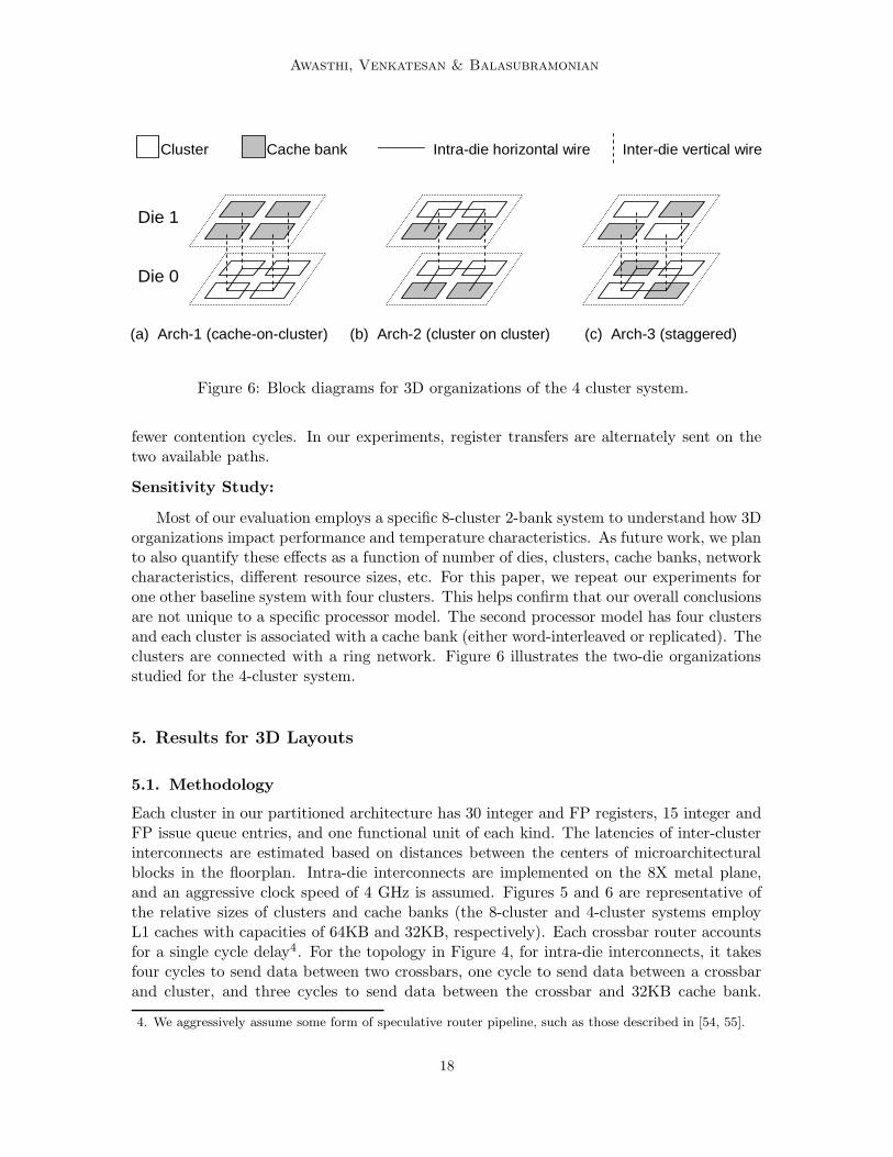
Sensitivity Study:
Most of our evaluation employs a specific 8-cluster 2-bank system to understand how 3Dorganizations impact performance and temperature characteristics. As future work, we planto also quantify these effects as a function of number of dies, clusters, cache banks, networkcharacteristics, different resource sizes, etc. For this paper, we repeat our experiments forone other baseline system with four clusters. This helps confirm that our overall conclusionsare not unique to a specific processor model. The second processor model has four clustersand each cluster is associated with a cache bank (either word-interleaved or replicated). Theclusters are connected with a ring network. Figure 6 illustrates the two-die organizationsstudied for the 4-cluster system.
5. Results for 3D Layouts
5.1. Methodology
Each cluster in our partitioned architecture has 30 integer and FP registers, 15 integer andFP issue queue entries, and one functional unit of each kind. The latencies of inter-clusterinterconnects are estimated based on distances between the centers of microarchitecturalblocks in the floorplan. Intra-die interconnects are implemented on the 8X metal plane,and an aggressive clock speed of 4 GHz is assumed. Figures 5 and 6 are representative ofthe relative sizes of clusters and cache banks (the 8-cluster and 4-cluster systems employL1 caches with capacities of 64KB and 32KB, respectively). Each crossbar router accountsfor a single cycle delay4. For the topology in Figure 4, for intra-die interconnects, it takesfour cycles to send data between two crossbars, one cycle to send data between a crossbarand cluster, and three cycles to send data between the crossbar and 32KB cache bank.
4. We aggressively assume some form of speculative router pipeline, such as those described in [54, 55].
18
Understanding the Impact of 3D Stacked Layouts on ILP
All vertical inter-die interconnects are assumed to have a single cycle latency due to theirextremely short length (10µm [14]). For intra-die interconnects in the 4-cluster organization,the inter-crossbar latency is two cycles. F2F bonding allows a relatively high inter-die viadensity [14] because of which we assume that the inter-die bandwidth is not a limitingconstraint for our experiments. The Wattch power models are employed to compute powerconsumption of each microarchitectural block. The contribution of leakage to total chippower is roughly 20%. Interconnect power (summarized in Table 8) is based on values for8X minimum-width wires [56] and a generic Network-on-Chip router [14].
Parameter Value
Router+Xbar Area 0.375 mm2 [14]Router+Xbar Power 119.55mW [14]
Wire Power/Length(mW/mm) 1.25 (8X), 1.40 (4X)
Table 8: Interconnect parameters.
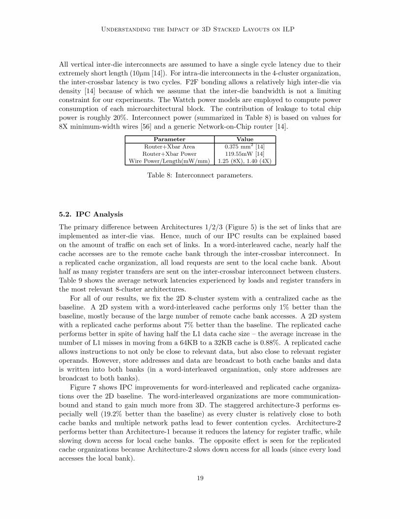
5.2. IPC Analysis
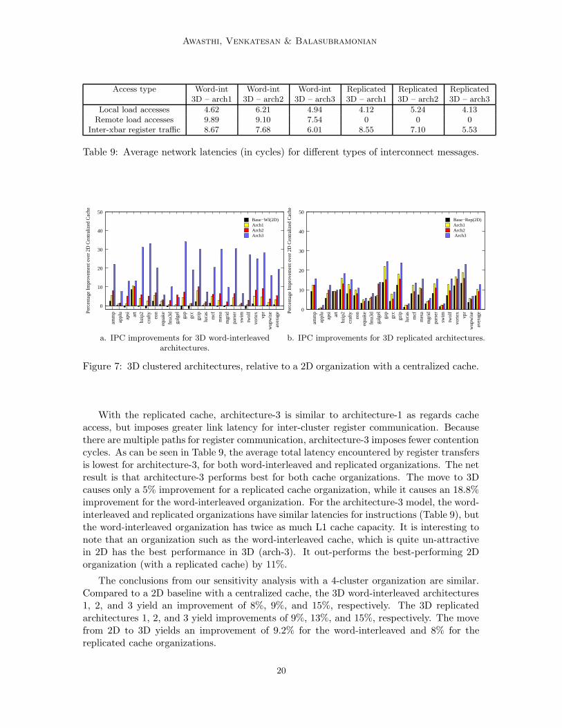
The primary difference between Architectures 1/2/3 (Figure 5) is the set of links that areimplemented as inter-die vias. Hence, much of our IPC results can be explained basedon the amount of traffic on each set of links. In a word-interleaved cache, nearly half thecache accesses are to the remote cache bank through the inter-crossbar interconnect. Ina replicated cache organization, all load requests are sent to the local cache bank. Abouthalf as many register transfers are sent on the inter-crossbar interconnect between clusters.Table 9 shows the average network latencies experienced by loads and register transfers inthe most relevant 8-cluster architectures.
For all of our results, we fix the 2D 8-cluster system with a centralized cache as thebaseline. A 2D system with a word-interleaved cache performs only 1% better than thebaseline, mostly because of the large number of remote cache bank accesses. A 2D systemwith a replicated cache performs about 7% better than the baseline. The replicated cacheperforms better in spite of having half the L1 data cache size – the average increase in thenumber of L1 misses in moving from a 64KB to a 32KB cache is 0.88%. A replicated cacheallows instructions to not only be close to relevant data, but also close to relevant registeroperands. However, store addresses and data are broadcast to both cache banks and datais written into both banks (in a word-interleaved organization, only store addresses arebroadcast to both banks).
Figure 7 shows IPC improvements for word-interleaved and replicated cache organiza-tions over the 2D baseline. The word-interleaved organizations are more communication-bound and stand to gain much more from 3D. The staggered architecture-3 performs es-pecially well (19.2% better than the baseline) as every cluster is relatively close to bothcache banks and multiple network paths lead to fewer contention cycles. Architecture-2performs better than Architecture-1 because it reduces the latency for register traffic, whileslowing down access for local cache banks. The opposite effect is seen for the replicatedcache organizations because Architecture-2 slows down access for all loads (since every loadaccesses the local bank).
19
Awasthi, Venkatesan & Balasubramonian
Access type Word-int Word-int Word-int Replicated Replicated Replicated3D – arch1 3D – arch2 3D – arch3 3D – arch1 3D – arch2 3D – arch3
Local load accesses 4.62 6.21 4.94 4.12 5.24 4.13Remote load accesses 9.89 9.10 7.54 0 0 0
Inter-xbar register traffic 8.67 7.68 6.01 8.55 7.10 5.53
Table 9: Average network latencies (in cycles) for different types of interconnect messages.
Base−WI(2D)Arch1Arch2Arch3
0
10
20
30
40
50
aver
age
wup
wis
evp
rvo
rtex
twol
fsw
impa
rser
mgr
idm
esa
mcf
luca
sgz
ipgc
cga
pga
lgel
fma3
deq
uakeeon
craf
tybz
ip2art
apsi
appl
uam
mpPe
rcen
tage
Im
prov
emen
t ove
r 2D
Cen
tral
ized
Cac
he
a. IPC improvements for 3D word-interleavedarchitectures.
Base−Rep(2D)Arch1Arch2 Arch3
0
10
20
30
40
50
aver
age
wup
wis
evp
rvo
rtex
twol
fsw
impa
rser
mgr
idm
esa
mcf
luca
sgz
ipgc
cga
pga
lgel
fma3
deq
uakeeon
craf
tybz
ip2art
apsi
appl
uam
mpPe
rcen
tage
Im
prov
emen
t ove
r 2D
Cen
tral
ized
Cac
he
b. IPC improvements for 3D replicated architectures.
Figure 7: 3D clustered architectures, relative to a 2D organization with a centralized cache.
With the replicated cache, architecture-3 is similar to architecture-1 as regards cacheaccess, but imposes greater link latency for inter-cluster register communication. Becausethere are multiple paths for register communication, architecture-3 imposes fewer contentioncycles. As can be seen in Table 9, the average total latency encountered by register transfersis lowest for architecture-3, for both word-interleaved and replicated organizations. The netresult is that architecture-3 performs best for both cache organizations. The move to 3Dcauses only a 5% improvement for a replicated cache organization, while it causes an 18.8%improvement for the word-interleaved organization. For the architecture-3 model, the word-interleaved and replicated organizations have similar latencies for instructions (Table 9), butthe word-interleaved organization has twice as much L1 cache capacity. It is interesting tonote that an organization such as the word-interleaved cache, which is quite un-attractivein 2D has the best performance in 3D (arch-3). It out-performs the best-performing 2Dorganization (with a replicated cache) by 11%.
The conclusions from our sensitivity analysis with a 4-cluster organization are similar.Compared to a 2D baseline with a centralized cache, the 3D word-interleaved architectures1, 2, and 3 yield an improvement of 8%, 9%, and 15%, respectively. The 3D replicatedarchitectures 1, 2, and 3 yield improvements of 9%, 13%, and 15%, respectively. The movefrom 2D to 3D yields an improvement of 9.2% for the word-interleaved and 8% for thereplicated cache organizations.
20
Understanding the Impact of 3D Stacked Layouts on ILP
Base(2D)Arch1Arch2 Arch3
0
20
40
60
80
100
120
140
aver
age
wup
wis
evp
rvo
rtex
twol
fsw
impa
rser
mgr
idm
esa
mcf
luca
sgz
ipgc
cga
pga
lgel
fma3
deq
uakeeon
craf
tybz
ip2
art
apsi
appl
uam
mp
Pea
k T
empe
ratu
re o
f H
otte
st U
nit (
Cel
sius
)
a. Peak temperature of hottest on-chip unit (celsius).
Base(2D)Arch1Arch2Arch3
0
20
40
60
80
100
120
140
aver
age
wup
wis
evp
rvo
rtex
twol
fsw
impa
rser
mgr
idm
esa
mcf
luca
sgz
ipgc
cga
pga
lgel
fma3
deq
uakeeon
craf
tybz
ip2
art
apsi
appl
uam
mp
Ave
rage
Tem
pera
ture
of
Hot
test
Uni
t(C
elsi
us)
b. Average temperature of hottest on-chipunit(Celsius).
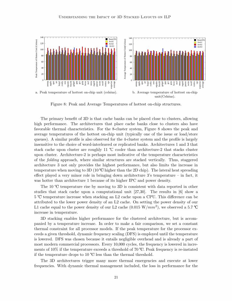
Figure 8: Peak and Average Temperatures of hottest on-chip structures.
The primary benefit of 3D is that cache banks can be placed close to clusters, allowinghigh performance. The architectures that place cache banks close to clusters also havefavorable thermal characteristics. For the 8-cluster system, Figure 8 shows the peak andaverage temperatures of the hottest on-chip unit (typically one of the issue or load/storequeues). A similar profile is also observed for the 4-cluster system and the profile is largelyinsensitive to the choice of word-interleaved or replicated banks. Architectures 1 and 3 thatstack cache upon cluster are roughly 11 � cooler than architecture-2 that stacks clusterupon cluster. Architecture-2 is perhaps most indicative of the temperature characteristicsof the folding approach, where similar structures are stacked vertically. Thus, staggeredarchitecture 3 not only provides the highest performance, but also limits the increase intemperature when moving to 3D (10 � higher than the 2D chip). The lateral heat spreadingeffect played a very minor role in bringing down architecture 3’s temperature – in fact, itwas hotter than architecture 1 because of its higher IPC and power density.
The 10 � temperature rise by moving to 3D is consistent with data reported in otherstudies that stack cache upon a computational unit [27,30]. The results in [6] show a5 � temperature increase when stacking an L2 cache upon a CPU. This difference can beattributed to the lower power density of an L2 cache. On setting the power density of ourL1 cache equal to the power density of our L2 cache (0.015 W/mm2), we observed a 5.7 �increase in temperature.
3D stacking enables higher performance for the clustered architecture, but is accom-panied by a temperature increase. In order to make a fair comparison, we set a constantthermal constraint for all processor models. If the peak temperature for the processor ex-ceeds a given threshold, dynamic frequency scaling (DFS) is employed until the temperatureis lowered. DFS was chosen because it entails negligible overhead and is already a part ofmost modern commercial processors. Every 10,000 cycles, the frequency is lowered in incre-ments of 10% if the temperature exceeds a threshold of 70 � . Peak frequency is re-instatedif the temperature drops to 10 � less than the thermal threshold.
The 3D architectures trigger many more thermal emergencies and execute at lowerfrequencies. With dynamic thermal management included, the loss in performance for the
21
Awasthi, Venkatesan & Balasubramonian
best-performing 2D organization and the best-performing 3D architecture-3 was 4% and10%, respectively. As a result, the best-performing 3D organization now out-performs thebest-performing 2D organization by only 5%.
The results in this section indicate that the 3D stacking approach can improve ILPfor aggressive superscalar implementations. We observed a 11% IPC improvement for thedescribed 8-cluster model and this improvement can be boosted to 15% if we aggressivelyassume zero-cycle delays for inter-die interconnects (instead of the single cycle delay assumedin the above experiments). However, some of this benefit disappears if we limit the processorto a fixed thermal constraint. In order to mine the available ILP, the chip will have to bepackaged for a higher cooling capacity.
6. Conclusions
3D technology has the potential to improve microprocessor performance, power, and costin different ways. This paper focuses on the stacking approach, where each pipeline stageis a 2D circuit and 3D is leveraged to reduce wire lengths between pipeline stages. Whilerecent studies have shown that such 3D implementations of complex pipelines can yield15% performance improvements [15], we show that simpler pipelines stand to gain less from3D. Few wire delays in traditional superscalars impose a non-trivial performance penaltyand 2D layouts can mitigate their effects with good floorplanning. A partitioned architec-ture is an example of a high-ILP processor that suffers from costly wire delays in a 2Dplanar implementation. We show that a word-interleaved L1 cache with a staggered 3Dplacement performs 11% better than the best-performing 2D layout, while also causing arelatively low (10 � ) increase in temperature. However, if we maintain a constant thermalconstraint, some of this performance benefit is lost. The key contributions of the paper canbe summarized as follows:
� This work is the first to integrate many varied aspects (loop analysis, automatedfloorplanning, distributed caches) in determining the benefit of 3D for single coreperformance.
� We present the most comprehensive analysis of the impact of wire delays on criticalprocessor loops (including various pipeline optimizations and SMT cores).
� This is the first body of work to carry out a detailed design space exploration of 3Dclustered architectures. We conclude that the staggered cluster-cache layout providesthe best performance and temperature.
� Unlike most prior work, our results are largely negative. We therefore argue that theresearch community should moderate their enthusiasm for the performance potentialof 3D for a single core.
We conclude that unless aggressive high-ILP processors are designed with superior cool-ing capacities, it may be difficult to leverage the 3D stacking approach for higher single-coreperformance. It is too early to tell if the 3D folding approach is perhaps a better path forhigher ILP. 3D technology continues to hold promise for other applications, such as reduc-ing inter-core latencies in a CMP, “snap-on” analysis engines, and stacked cache/memoryhierarchies for CMPs. We view these avenues as exciting future work.
22
Understanding the Impact of 3D Stacked Layouts on ILP
Acknowledgements
This work was supported in parts by NSF grant CCF-0430063 and NSF CAREER AwardCCF-0545959. We thank the anonymous reviewers and our shepherd, Dr. Alvin Lebeck,for many helpful suggestions to improve the work. We also thank Abhishek Ranjan for hiscontribution to early parts of this work.
References
[1] Semiconductor Industry Association, “International Technology Roadmap for Semi-conductors 2005.” http://www.itrs.net/Links/2005ITRS/Home2005.htm.
[2] N. Magen, A. Kolodny, U. Weiser, and N. Shamir, “Interconnect Power Dissipation ina Microprocessor,” in Proceedings of System Level Interconnect Prediction, February2004.
[3] Y. Xie, G. Loh, B. Black, and K. Bernstein, “Design Space Exploration for 3D Archi-tectures,” ACM Journal of Emerging Technologies in Computing Systems, vol. 2(2),pp. 65–103, April 2006.
[4] J. Rattner, “Predicting the Future,” 2005. Keynote at Intel Developer Forum (articleat http://www.anandtech.com/tradeshows/showdoc.aspx?i=2367&p=3).
[5] Samsung Electronics Corporation, “Samsung Electronics Develops World’s First Eight-Die Multi-Chip Package for Multimedia Cell Phones,” 2005. (Press release fromhttp://www.samsung.com).
[6] S. Mysore, B. Agrawal, N. Srivastava, S. Lin, K. Banerjee, and T. Sherwood, “Intro-spective 3D Chips,” in Proceedings of ASPLOS-XII, October 2006.
[7] K. Puttaswamy and G. Loh, “Implementing Caches in a 3D Technology for High Per-formance Processors,” in Proceedings of ICCD, October 2005.
[8] K. Puttaswamy and G. Loh, “Dynamic Instruction Schedulers in a 3-Dimensional In-tegration Technology,” in Proceedings of GLSVLSI, April 2006.
[9] K. Puttaswamy and G. Loh, “Implementing Register Files for High-Performance Mi-croprocessors in a Die-Stacked (3D) Technology,” in Proceedings of ISVLSI, March2006.
[10] K. Puttaswamy and G. Loh, “The Impact of 3-Dimensional Integration on the Designof Arithmetic Units,” in Proceedings of ISCAS, May 2006.
[11] P. Reed, G. Yeung, and B. Black, “Design Aspects of a Microprocessor Data Cacheusing 3D Die Interconnect Technology,” in Proceedings of International Conference onIntegrated Circuit Design and Technology, May 2005.
[12] Y.-F. Tsai, Y. Xie, N. Vijaykrishnan, and M. Irwin, “Three-Dimensional Cache DesignUsing 3DCacti,” in Proceedings of ICCD, October 2005.
23
Awasthi, Venkatesan & Balasubramonian
[13] G. Loi, B. Agrawal, N. Srivastava, S. Lin, T. Sherwood, and K. Banerjee, “A Thermally-Aware Performance Analysis of Vertically Integrated (3-D) Processor-Memory Hierar-chy,” in Proceedings of DAC-43, June 2006.
[14] F. Li, C. Nicopoulos, T. Richardson, Y. Xie, N. Vijaykrishnan, and M. Kandemir,“Design and Management of 3D Chip Multiprocessors Using Network-in-Memory,” inProceedings of ISCA-33, June 2006.
[15] B. Black, M. Annavaram, E. Brekelbaum, J. DeVale, L. Jiang, G. Loh, D. McCauley,P. Morrow, D. Nelson, D. Pantuso, P. Reed, J. Rupley, S. Shankar, J. Shen, andC. Webb, “Die Stacking (3D) Microarchitecture,” in Proceedings of MICRO-39, De-cember 2006.
[16] M. Awasthi and R. Balasubramonian, “Exploring the Design Space for 3D ClusteredArchitectures,” in Proceedings of the 3rd IBM Watson Conference on Interaction be-tween Architecture, Circuits, and Compilers, October 2006.
[17] G. Hinton, D. Sager, M. Upton, D. Boggs, D. Carmean, A. Kyker, and P. Roussel, “TheMicroarchitecture of the Pentium 4 Processor,” Intel Technology Journal, vol. Q1, 2001.
[18] E. Borch, E. Tune, B. Manne, and J. Emer, “Loose Loops Sink Chips,” in Proceedingsof HPCA, February 2002.
[19] J. Cong, A. Jagannathan, Y. Ma, G. Reinman, J. Wei, and Y. Zhang, “An AutomatedDesign Flow for 3D Microarchitecture Evaluation,” in Proceedings of ASP-DAC, Jan-uary 2006.
[20] K. Sankaranarayanan, S. Velusamy, M. Stan, and K. Skadron, “A Case for Thermal-Aware Floorplanning at the Microarchitectural Level,” Journal of ILP, vol. 7, October2005.
[21] E. Sprangle and D. Carmean, “Increasing Processor Performance by ImplementingDeeper Pipelines,” in Proceedings of ISCA-29, May 2002.
[22] G. Reinman, T. Austin, and B. Calder, “A Scalable Front-End Architecture for FastInstruction Delivery,” in Proceedings of ISCA-26, May 1999.
[23] R. Kessler, “The Alpha 21264 Microprocessor,” IEEE Micro, vol. 19, pp. 24–36,March/April 1999.
[24] W. Liao and L. He, “Full-Chip Interconnect Power Estimation and Simulation Consid-ering Concurrent Repeater and Flip-Flop Insertion,” in Proceedings of ICCAD, 2003.
[25] C. Long, L. Simonson, W. Liao, and L. He, “Floorplanning Optimization with Tra-jectory Piecewise-Linear Model for Pipelined Interconnects,” in Proceedings of DAC,2004.
[26] Y. Liu, A. Shayesteh, G. Memik, and G. Reinman, “Tornado Warning: The Perils ofSelective Replay in Multithreaded Processors,” in Proceedings of ICS, June 2005.
24
Understanding the Impact of 3D Stacked Layouts on ILP
[27] M. Ekpanyapong, J. Minz, T. Watewai, H. Lee, and S. Lim, “Profile-Guided Microar-chitectural Floorplanning for Deep Submicron Processor Design,” in Proceedings ofDAC-41, June 2004.
[28] W. Hung, Y. Xie, N. Vijaykrishnan, C. Addo-Quaye, T. Theocharides, and M. Irwin,“Thermal-Aware Floorplanning using Genetic Algorithms,” in Proceedings of ISQED,March 2005.
[29] D. Burger and T. Austin, “The Simplescalar Toolset, Version 2.0,” Tech. Rep. TR-97-1342, University of Wisconsin-Madison, June 1997.
[30] T. Sherwood, E. Perelman, G. Hamerly, and B. Calder, “Automatically CharacterizingLarge Scale Program Behavior,” in Proceedings of ASPLOS-X, October 2002.
[31] D. Tullsen, S. Eggers, J. Emer, H. Levy, J. Lo, and R. Stamm, “Exploiting Choice:Instruction Fetch and Issue on an Implementable Simultaneous Multithreading Pro-cessor,” in Proceedings of ISCA-23, May 1996.
[32] W. Hung, G. Link, Y. Xie, N. Vijaykrishnan, and M. Irwin, “Interconnect and Thermal-Aware Floorplanning for 3D Microprocessors,” in Proceedings of ISQED, March 2006.
[33] D. Wong and C. Liu, “A New Algorithm for Floorplan Design,” in Proceedings of the23rd ACM/IEEE conference on Design automation, pp. 101–107, 1986.
[34] D. Brooks, V. Tiwari, and M. Martonosi, “Wattch: A Framework for Architectural-Level Power Analysis and Optimizations,” in Proceedings of ISCA-27, pp. 83–94, June2000.
[35] K. Skadron, M. R. Stan, W. Huang, S. Velusamy, and K. Sankaranarayanan,“Temperature-Aware Microarchitecture,” in Proceedings of ISCA-30, pp. 2–13, 2003.
[36] K. Puttaswamy and G. Loh, “Thermal Analysis of a 3D Die-Stacked High-PerformanceMicroprocessor,” in Proceedings of GLSVLSI, April 2006.
[37] K. Banerjee and A. Mehrotra, “A Power-optimal Repeater Insertion Methodology forGlobal Interconnects in Nanometer Designs,” IEEE Transactions on Electron Devices,vol. 49, pp. 2001–2007, November 2002.
[38] W.-L. Hung, G. Link, Y. Xie, N. Vijaykrishnan, and M. J. Irwin, “Interconnect andthermal-aware floorplanning for 3d microprocessors,” isqed, vol. 0, pp. 98–104, 2006.
[39] R. Kumar, V. Zyuban, and D. Tullsen, “Interconnections in Multi-Core Architectures:Understanding Mechanisms, Overheads, and Scaling,” in Proceedings of the 32nd ISCA,June 2005.
[40] J. Collins and D. Tullsen, “Clustered Multithreaded Architectures – Pursuing BothIPC and Cycle Time,” in Proceedings of the 18th IPDPS, April 2004.
[41] A. El-Moursy, R. Garg, D. Albonesi, and S. Dwarkadas, “Partitioning Multi-ThreadedProcessors with a Large Number of Threads,” in Proceedings of ISPASS, March 2005.
25

Awasthi, Venkatesan & Balasubramonian
[42] K. Sankaralingam, R. Nagarajan, H. Liu, C. Kim, J. Huh, D. Burger, S. Keckler, andC. Moore, “Exploiting ILP, TLP, and DLP with the Polymorphous TRIPS Architec-ture,” in Proceedings of ISCA-30, June 2003.
[43] R. Balasubramonian, S. Dwarkadas, and D. Albonesi, “Dynamically Managing theCommunication-Parallelism Trade-Off in Future Clustered Processors,” in Proceedingsof ISCA-30, pp. 275–286, June 2003.
[44] R. Canal, J. M. Parcerisa, and A. Gonzalez, “Dynamic Code Partitioning for ClusteredArchitectures,” International Journal of Parallel Programming, vol. 29, no. 1, pp. 59–79, 2001.
[45] K. Farkas, P. Chow, N. Jouppi, and Z. Vranesic, “The Multicluster Architecture: Re-ducing Cycle Time through Partitioning,” in Proceedings of MICRO-30, pp. 149–159,December 1997.
[46] M. Taylor, W. Lee, J. Miller, D. Wentzlaff, I. Bratt, B. Greenwald, H. Hoffmann,P. Johnson, J. Kim, J. Psota, A. Raraf, N. Shnidman, V. Strumpen, M. Frank, S. Ama-rasinghe, and A. Agarwal, “Evaluation of the Raw Microprocessor: An Exposed-Wire-Delay Architecture for ILP and Streams,” in Proceedings of ISCA-31, June 2004.
[47] S. Palacharla, N. Jouppi, and J. Smith, “Complexity-Effective Superscalar Processors,”in Proceedings of ISCA-24, pp. 206–218, June 1997.
[48] A. Aggarwal and M. Franklin, “An Empirical Study of the Scalability Aspects of In-struction Distribution Algorithms for Clustered Processors,” in Proceedings of ISPASS,2001.
[49] R. Balasubramonian, “Cluster Prefetch: Tolerating On-Chip Wire Delays in ClusteredMicroarchitectures,” in Proceedings of ICS-18, June 2004.
[50] P. Racunas and Y. Patt, “Partitioned First-Level Cache Design for Clustered Microar-chitectures,” in Proceedings of ICS-17, June 2003.
[51] V. Zyuban and P. Kogge, “Inherently Lower-Power High-Performance Superscalar Ar-chitectures,” IEEE Transactions on Computers, March 2001.
[52] E. Gibert, J. Sanchez, and A. Gonzalez, “Effective Instruction Scheduling Techniquesfor an Interleaved Cache Clustered VLIW Processor,” in Proceedings of MICRO-35,pp. 123–133, November 2002.
[53] B. Black, D. Nelson, C. Webb, and N. Samra, “3D Processing Technology and itsImpact on IA32 Microprocessors,” in Proceedings of ICCD, October 2004.
[54] R. Mullins, A. West, and S. Moore, “Low-Latency Virtual-Channel Routers for On-Chip Networks,” in Proceedings of ISCA-31, May 2004.
[55] L.-S. Peh and W. Dally, “A Delay Model and Speculative Architecture for PipelinedRouters.,” in Proceedings of HPCA-7, 2001.
26

Understanding the Impact of 3D Stacked Layouts on ILP
[56] L. Cheng, N. Muralimanohar, K. Ramani, R. Balasubramonian, and J. Carter,“Interconnect-Aware Coherence Protocols for Chip Multiprocessors,” in Proceedingsof ISCA-33, June 2006.
27