Embed Size (px)
Citation preview
UNIT 1 By: Ajay Kumar Gautam
Asst. Prof.
Electronics & Communication Engineering
Dev Bhoomi Institute of Technology & Engineering, Dehradun
Saturday, August 04, 2012 UNIT 1
0

Syllabus
• Introduction to VLSI Technology: Classification if ICs,
Scale of integration, semiconductor and hybrid ICs
Features of ICs
• Crystal Growth: monolithic and hybrid ICs, crystal
growth, Czochralski technique of crystal growth, wafer
preparation and specifications, testing, measurements of
parameters of crystals, Fabrication steps
• Oxidation: Theory of growth of Silicon di oxide layer,
calculation of SiO2 thickness and oxidation kinetics, Dry
wet and high pressure oxidation, plasma oxidation
properties of oxidation, defects induced due to oxidation
Saturday, August 04, 2012 UNIT 1
1

Module 1: Introduction
to VLSI Technology Saturday, August 04, 2012 UNIT 1
2

What is a circuit?
• It is the combination of active & passive elements.
• Active elements are those, which can produce gain or can
amplify signals, like transistors or amplifiers.
• Passive elements doesn’t have this kind of capability
without active elements.
• This kind of circuit is known as discrete circuit.
Saturday, August 04, 2012 UNIT 1
3

What is an Integrated
Circuit?
• It is an electronic circuit, used almost in all electronic
equipment's.
• It is the combination of active & passive elements, when
placed on the same substrate, usually Si.
• 4 MB DRAM chip is the best example of IC.
• Active elements in an IC can be transistors (BJT or
MOSFET) & are most important part of any circuit.
Saturday, August 04, 2012 UNIT 1
4

Moore’s Law
• Gordon Moore, in 1965 an integrated circuit pioneer and
co-founder of Intel corporation predicted that, the number
of transistors on chip will be double by every 18 months.
• In 1965, Intel fabricated its first processor on 25 µm
technology.
• In 2000, Intel fabricated processors on 0.18 µm technology.
• Now-a-days technology used for IC fabrication is 90 nm to
40 nm.
• 90 nm for computer processor
• 40 nm for smart phone.
Saturday, August 04, 2012 UNIT 1
5

Classification of ICs
• There are 5 ways to classify Integrated Circuits.
1. By fabrication
2. By complexity
3. By packing density
4. By application
5. By technology
Saturday, August 04, 2012 UNIT 1
6

1. By Fabrication
a) Monolithic IC – IC which are entirely a single chip of
semiconductor usually Si, are known as monolithic circuit.
b) Hybrid IC – IC which contain one or more monolithic
circuit or individual transistors bounded to an insulating
substrate with passive elements.
Saturday, August 04, 2012 UNIT 1
7

2. By Complexity
a) SSI – components 1 – 10, flip flops & gates.
b) MSI - components 10 – 100, registers & counters.
c) LSI – components 100 – 10,000, ROM, decoders.
d) VLSI – more than 10,000 components, microprocessors
& high capacity memories.
e) ULSI – more than 3 million components.
Saturday, August 04, 2012 UNIT 1
8

3. By Packing Density
• Packing density is defined as no. of components contained
in the unit area of the chip, & is given by;
P = log Q,
• where P = packing density & Q = Scale of integration.
a) SSI P < 1
b) MSI 1 < P < 2
c) LSI 2 < P < 4
d) VLSI 4 < P < 6
e) ULSI P > 6
Saturday, August 04, 2012 UNIT 1
9

4. By Application
a) Analog IC – it performs amplification & other functions
on analog signals linearly. Ex: OP – AMP.
b) Digital IC – it performs operations with discrete
quantities, i.e., information for digital IC is represented by
binary digit. Ex: computer calculator & microprocessor.
Saturday, August 04, 2012 UNIT 1
10

5. By Technology
1. BJT Technology – it is used for high speed.
2. MOSFET Technology - it is used for high packing
density.
3. BiCMOS Technology – it is used for high speed as well as
high packing density.
Saturday, August 04, 2012 UNIT 1
11

Advantages of ICs
1. Increased reliability, due to lesser no. of connections
2. Extremely small size, due to fabrication of various circuits
onto a single chip of semiconductor.
3. Lesser weight & space requirements.
4. Low power requirement.
5. Lower cost.
Saturday, August 04, 2012 UNIT 1
12

Disadvantages of ICs
1. ICs are not flexible.
2. It is not possible to produce high power ICs greater than
10 watt.
3. Fabrication of high value capacitors, inductors and
transformers is not possible.
4. If any component in an IC goes out of order, the whole
IC has to be replaced with new one.
Saturday, August 04, 2012 UNIT 1
13

Features of ICs
1. An IC performs complex functions, whereas elementary
devices ( transistors ) can perform same functions only in
combination with other components.
2. Reliability and cost are not affected by increase in
functional complexity of ICs.
3. The size of most of the ICs are comparable with discrete
transistors, but the function performed by an IC is much
more complex.
Saturday, August 04, 2012 UNIT 1
14

Cond….
4. In an IC, the adjacent components are spaced mostly 50 –
100 µm apart, but the components doesn’t change their
electrical, chemical & physical properties. Whereas the
parameters are changed in different. Ex: Change in
temperature coefficient due to variations in temperature.
5. In an IC, interconnection of individual elements is made
through metallization ( i.e. without soldering and welding).
Hence it is more reliable in comparison to discrete
components in which large number of soldering and
welding is used.
Saturday, August 04, 2012 UNIT 1
15

Silicon Vs. Germanium
1. Si devices can operate upto 1500 C as compared to 1000 C
for Ge.
2. Si grows a stable oxide, which is important in fabrication
if IC as compared to Ge oxide which is unsuited for
device applications.
3. Silicon is cheaper than Ge.
4. Silicon is easily available near sea beaches as raw material
for silicon wafer preparation.
5. Silicon has low leakage current as compared to that of
Ge.
Saturday, August 04, 2012 UNIT 1
16

Module 2:
Crystal Growth Saturday, August 04, 2012 UNIT 1
17
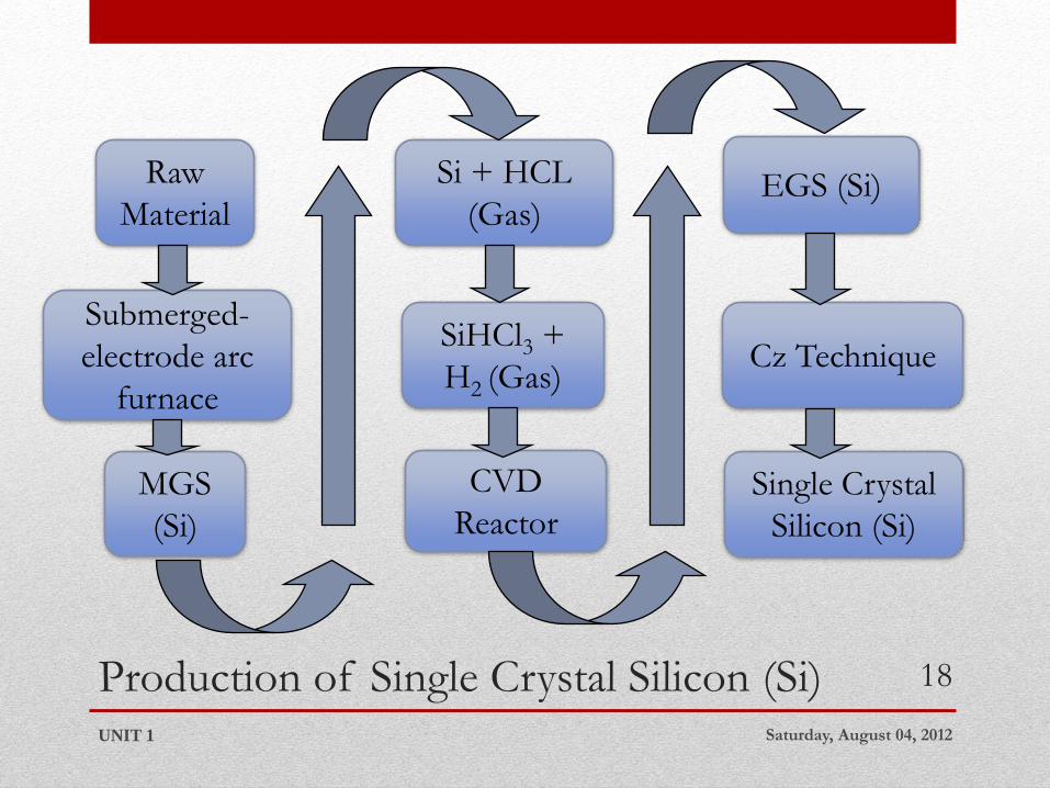
Production of Single Crystal Silicon (Si) Saturday, August 04, 2012 UNIT 1
18
Raw
Material
MGS
(Si)
SiHCl3 +
H2 (Gas)
EGS (Si) Si + HCL
(Gas)
CVD
Reactor Single Crystal
Silicon (Si)
Submerged-
electrode arc
furnace
Cz Technique

Cond….
• Silicon occurs naturally in form of silica and silicates.
• It is most important semiconductor for the electronic
industry.
• More than 95% semiconductor devices are made of silicon.
• It is easy to grow SiO2
Saturday, August 04, 2012 UNIT 1
19

Electronic Grade Silicon
• It is polycrystalline material of high purity.
• EGS is the raw material for the preparation of single crystal
silicon.
• EGS is the one of the purist material available for
electronics industry.
• To obtain EGS, we require a multistep process.
• MGS ( Metallurgical Grade Silicon ) is produced in
submerged – electrode.
• The furnace is charged with quartzite and carbon.
Saturday, August 04, 2012 UNIT 1
20

Fig: Submerged – electrode arc furnace
for production of MGS Saturday, August 04, 2012 UNIT 1
21

Cond….
• Quartzite is the pure form of sand i.e., SiO2.
• In furnace large number of reactions takes place.
• The overall reaction is,
SiC (Solid)+SiO2 (solid) -> Si (liquid) + SiO (gas) + CO (gas).
• This process requires 13 Kwh/kg of power.
• MGS available in this process is then solidified at a purity
of 98%.
• The next step is to pulverize the silicon mechanically.
Saturday, August 04, 2012 UNIT 1
22

Cond….
• Now react it with anhydrous hydrogen chloride to form
trichlorosilane (SiHCl3)
Si (solid) +3HCl -> SiHCl3 (gas)+H2 (gas)+Heat
• The reaction takes place at temperature of 300oC using a
catalyst.
• EGS is prepared from the purified SiHCl3 in a Chemical
Vapor Deposition (CVD) process.
Saturday, August 04, 2012 UNIT 1
23

Fig: CVD Reactor used for production of EGS
Saturday, August 04, 2012 UNIT 1
24

Cond….
• The chemical reaction is a hydrogen reduction of
trichlorosilane.
SiHCl3 (gas) + H2 (gas)-> Si (Solid) + 3HCl (gas)
• A slim rod of silicon serves as nucleation point for the
deposition of silicon.
• This process takes many hours & will give polycrystalline
silicon (EGS) on slim rod of silicon.
• The polycrystalline silicon (EGS) is 0.2 m or greater in
diameter & several meter in length.
• This EGS can be cut from these rod as single chunks (solid
piece).
Saturday, August 04, 2012 UNIT 1
25

Czochralski (Cz)technique
of crystal growth
• Polycrystalline silicon may contain many defects.
• So in order to fabricate an IC, it must be nearly perfect.
• Therefore we need to produce single crystal silicon.
• Cz process is the basic technique to produce the single
crystal silicon.
• Cz process is a liquid-solid mono-component system.
Saturday, August 04, 2012 UNIT 1
26

Fig: Cz Crystal Grower Saturday, August 04, 2012 UNIT 1
27

Cond….
• In the Cz grower, we have big quartz chamber, with gas
inlet and outlet & some pumps.
• Pumps are required to maintain the pressure in quartz
chamber.
• There is one another opening through which a pull rod is
passed.
• There is a big cup (crucible), in which the poly crystalline
silicon is placed in order to grow single crystal silicon.
• Crucible is usually made of quartz which is SiO2.
Saturday, August 04, 2012 UNIT 1
28

Cond….
• Some oxide may come to the crystal from the crucible, so
this crucible can be usually used once.
• This is because when, Cz grower get cooled down, then
because of the thermal mismatch the quartz crucible
cracks.
• This quartz crucible is usually placed inside a graphite
susceptor, which is outer jacket to the quartz crucible.
• The susceptor, is surrounded by RF heating elements.
Saturday, August 04, 2012 UNIT 1
29

Cond….
• Cz crystal grower has mainly four subsystem.
1) Furnace
2) Crystal pulling mechanism
3) Ambient Control
4) Control system
Saturday, August 04, 2012 UNIT 1
30

Cond….
• Furnace is the most important part of the Cz crystal
grower.
• The furnace is heated to a temperature of 1690 K, which is
slightly greater than melting point (1685 K)of silicon.
• Inside the furnace, we have a quartz crucible, a quartz
susceptor, a heater and cooling for outer quartz chamber.
Saturday, August 04, 2012 UNIT 1
31

Cond….
• The crystal pulling mechanism includes pull rod, a seed
crystal and rotation mechanism (CCW).
• At the end of the pull rod, the small seed crystal is fixed in
a chuck.
• The pull rod is rotated (CCW) and pulled up very slowly at
the same time, the quartz crucible is rotated in the opposite
direction (CW).
Saturday, August 04, 2012 UNIT 1
32

Cond….
• The ambient control is very important in the Cz crystal
grower.
• There must not be oxygen inside the quartz crucible,
because it will react with the polycrystalline silicon (EGS).
• So, the quartz chamber is filled up with an inert ambient,
i.e., organ helium or nitrogen.
Saturday, August 04, 2012 UNIT 1
33

Cond….
• The control system provides control of temperature,
crystal diameter, pull rate and the rotation speed.
• The control system may have sensors and outputs.
Saturday, August 04, 2012 UNIT 1
34

Cond….
• For the crystal growth, the polycrystalline silicon is placed
inside the quartz crucible & the ambient condition is
created.
• The furnace is heated to a temperature of 1690 K, the
polycrystalline silicon (EGS) gets heated.
• A controlled amount of dopant (boron or phosphorus) is
added to the melt to make the silicon either P type or N
type.
• Initially the seed crystal is not in contact with the melt.
Saturday, August 04, 2012 UNIT 1
35

Cond….
• The pull rod is rotated and lowered gradually till the seed
crystal touches the melt surface.
• While the crucible is rotated in the opposite direction.
• When molten silicon is attached to the seed crystal and it
becomes identical to the seed, & get solidified.
• After that the solidified silicon crystal can be pulled up.
• So, using the Cz technique, we have cylindrical single crystal
silicon known as ingot.
Saturday, August 04, 2012 UNIT 1
36

Cond….
• By controlling temperature and pulling rate, desired
diameter of the silicon ingot can be obtained.
• The ingot is cooled and is removed to make wafers.
• Usually the ingot has diameter of 200 mm and length 1000
mm.
• The pull rate must be adjusted very carefully.
Saturday, August 04, 2012 UNIT 1
37

Saturday, August 04, 2012 UNIT 1
38

Saturday, August 04, 2012 UNIT 1
39

Saturday, August 04, 2012 UNIT 1
40

Saturday, August 04, 2012 UNIT 1
41

How the Pull Rate is
adjusted
• The pull rate should me adjusted carefully, so that we can
get good quality of crystal.
• If the pull rate and thermal conditions are not adjusted, the
seed crystal can also get melted.
• So, the Cz technique is much more complicated technique.
• Since, the Cz technique is liquid solid monocomponent
system, there is some heat transfer.
• So, we need to consider the Heat transfer Equation.
Saturday, August 04, 2012 UNIT 1
42

Cond…. Saturday, August 04, 2012 UNIT 1
43

Cond… Saturday, August 04, 2012 UNIT 1
44

Cond… Saturday, August 04, 2012 UNIT 1
45

Dopant incorporation
during the crystal growth
• Dopants are added to the melt in order to provide a
controlled N or P doping level in the wafer.
• Dopant incorporation process is accomplished by dopant
segregation.
• Generally impurities are added to the melt.
• This process is known as segregation.
• The degree of segregation is characterized by segregation
coefficient k0, & is given by:
Saturday, August 04, 2012 UNIT 1
46
0s
l
Ck
C

Cond…
• Where, Cs & Cl are the equilibrium concentrations of the
impurities of the impurities in the solid (crystal) & liquid
(melt) respectively near the solid-liquid interface.
• For most of the common impurities k0 < 1, i.e., Cs < Cl.
• It means impurities are not coming into solid, they are
rejected by the solid.
• Note that purpose of incorporating impurities to the melt
is only to change its electrical properties, i.e., to make it
either N or P type.
Saturday, August 04, 2012 UNIT 1
47
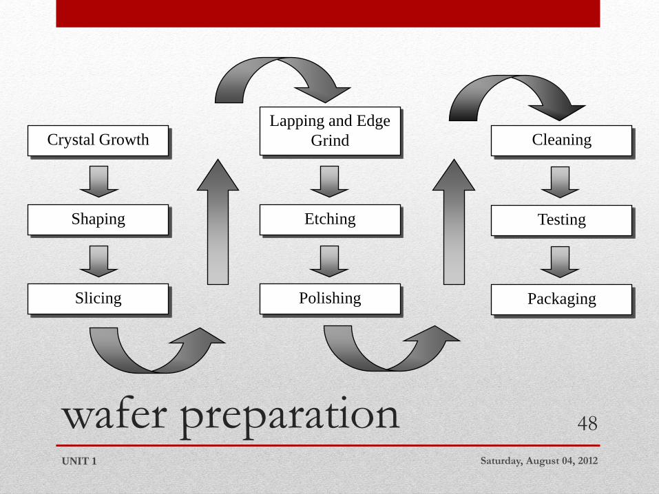
wafer preparation Saturday, August 04, 2012 UNIT 1
48
Crystal Growth
Shaping
Slicing
Lapping and Edge
Grind
Etching
Polishing
Cleaning
Testing
Packaging

Shaping
• The silicon crystal obtained after Cz process is called
“ingot”.
• The first shaping operation removes the seed and tang ends
from the ingot.
• The ingot surface is then grounded throughout to an exact
diameter.
Saturday, August 04, 2012 UNIT 1
49

Fig: Shaping Saturday, August 04, 2012 UNIT 1
50
Flat grind
Diameter grind
Preparing crystal ingot for grinding

Wafer Slicing
• Once the ingot surface is made smooth, ingot is sliced in
wafers by high speed “diamond saw”.
• Slicing is done by inner diameter sawing using a diamond
saw.
• It is rotated at a high speed and then moved across the
ingot to obtain wafer slices.
• Slicing is done very slowly.
• Thicker wafers are usually preferred.
Saturday, August 04, 2012 UNIT 1
51

Lapping & Edge Grind
• After slicing there is a variation in the thickness of the
sliced wafer.
• So, it can’t be used directly for IC fabrication.
• The wafers a mechanically lapped on both the sides.
• Lapping is done in order to remove the cracked or damaged
surface of the wafer.
• After lapping edge grinding takes place.
Saturday, August 04, 2012 UNIT 1
52

Fig: Lapping Machine Saturday, August 04, 2012 UNIT 1
53

Etching
• Etching is the process of selectively removing unwanted
semiconductor material from the wafer.
• Wet etching: chemical solution is used.
• Dry Etching: sputtering method is used.
• Chemical etching removes the remaining damaged and
contaminated regions of the wafer.
• A mixture of HF & HNO3, is used for chemical etching.
Saturday, August 04, 2012 UNIT 1
54

Wafer Polishing
• The purpose of polishing is to provide smooth surface of
the wafer.
• The wafer surface is polished to mirror like finish.
Saturday, August 04, 2012 UNIT 1
55

Fig: Wafer Polishing Saturday, August 04, 2012 UNIT 1
56

Cleaning
• Wafers are cleaned and dried for use in IC fabrication.
• The final wafer thickness is about one third of the sliced
wafer.
Saturday, August 04, 2012 UNIT 1
57

Testing
• Wafer testing is a step performed during semiconductor
device fabrication.
• During this step, performed before a wafer is sent to die
preparation.
• All individual integrated circuits that are present on the
wafer are tested for functional defects.
• The wafer testing is performed by a piece of test
equipment called a wafer prober.
Saturday, August 04, 2012 UNIT 1
58
Packaging
• Packaging is done in order to protect the wafers from
moisture & contaminants.
• The completed packages are inspected, sealed, and marked
with a special ink to indicate product type, date, package
code, and speed.
Saturday, August 04, 2012 UNIT 1
59

IC Fabrication steps Saturday, August 04, 2012 UNIT 1
60
Wafer
preparation
oxidation
Diffusion
Metallization Photolithography
Etching Packaging
Epitaxy Testing

Epitaxy
• Epitaxy is a combination of two Greek words, epi means
upon and taxis means ordered.
• It is a process of growing thin crystalline layer on a
crystalline substrate.
• 2 kind of epitaxial process CVD & MBE.
• CVD is a chemical process whereas in MBE, there is no
chemical reaction involved.
• 2 kind of epitaxy, homoepitaxy & heteroepitaxy.
Saturday, August 04, 2012 UNIT 1
61

Oxidation
• Process of growing film on the surface of silicon.
• Takes place at 1000 – 12000 C.
• It serves as mask against diffusion of dopants.
• It is used as isolation between two device.
• It is used as Gate oxide for MOS devices.
• It provides electrical isolation of multilevel metallization.
• It as used as surface passivation.
Saturday, August 04, 2012 UNIT 1
62

Photolithography
• Process of transferring geometrical pattern on the glass
plate to the surface of the wafer.
• To transfer the pattern, the wafer is coated with light
sensitive material called photoresist.
• The photoresist is then placed on the wafer.
• This is exposed to ultraviolet light.
• The photoresist under the opaque regions of the glass plate
is unaffected.
Saturday, August 04, 2012 UNIT 1
63

Diffusion
• Process of introducing impurities into selecting regions of
a wafer to form junctions.
• Diffusion allows the formation of source and drain regions.
Saturday, August 04, 2012 UNIT 1
64
Etching
• Etching is the process of selectively removing unwanted
semiconductor material from the wafer.
• Wet etching: chemical solution is used.
• Dry Etching: sputtering method is used.
• Chemical etching removes the remaining damaged and
contaminated regions of the wafer.
• A mixture of HF & HNO3, is used for chemical etching.
Saturday, August 04, 2012 UNIT 1
65

Metallization
• Process of interconnecting various components to form
desired IC.
• Initially metal is deposited over the entire surface of the
wafer.
• After that etching takes place.
• Metallization is usually done by sputtering method.
Saturday, August 04, 2012 UNIT 1
66

Testing
• Wafer testing is a step performed during semiconductor
device fabrication.
• During this step, performed before a wafer is sent to die
preparation.
• All individual integrated circuits that are present on the
wafer are tested for functional defects & electrical
properties of the device.
• The wafer testing is performed by a piece of test
equipment called a wafer prober.
Saturday, August 04, 2012 UNIT 1
67

Packaging
• Packaging is done in order to protect the wafers from
moisture & contaminants.
• The completed packages are inspected, sealed, and marked
with a special ink to indicate product type, date, package
code, and speed.
Saturday, August 04, 2012 UNIT 1
68

Measurements of
parameters of crystals
• Resistivity measurements are performed on flat ends of the
crystal by four-probe technique.
• Current I (mA) is passed through the outer probes and
voltage V (mV) measured between the inner probes.
• The resistivity ρ (Ω-cm) is measured by the formula;
ρ=(V/I) 2πS
Saturday, August 04, 2012 UNIT 1
69

Fig: Four-point probe measurement on crystal end
Saturday, August 04, 2012 UNIT 1
70

Module 3: Oxidation Saturday, August 04, 2012 UNIT 1
71
Introduction
• Process of growing film on the surface of silicon.
• Takes place at 1000 – 12000 C.
• Oxides are used as
1. Masking element against diffusion of dopants.
2. Gate oxide in MOS devices
3. Isolation between devices
4. Electrical isolation of multilevel metallization
5. Used as surface passivation
Saturday, August 04, 2012 UNIT 1
72

Cond…
• Since silicon has great affinity for oxygen, so it is very easy
to oxidize silicon.
• There are a lot of methods for oxidation.
• If silicon is boiled in nitric acid, oxide layer will be formed,
it is called chemical oxidation.
• Thermal oxidation is another method & is widely used in
VLSI technology.
Saturday, August 04, 2012 UNIT 1
73

Thermal Oxidation
• For thermal oxidation, take Si sample.
• Put it inside a furnace.
• Raise the temperature.
• Allow either oxygen or water vapor.
• Silicon will react either with oxygen or water to form SiO2.
• Si+O2 -> SiO2 Dry Oxidation
• Si+2H2O -> SiO2+2H2 Wet Oxidation
Saturday, August 04, 2012 UNIT 1
74

Oxidation Growth
Kinetics Saturday, August 04, 2012 UNIT 1
75

Cond…
• Consider the Groove model for thermal oxidation of the
silicon.
• Initially SiO2 layer is not present.
• We have oxidizing species in the gas.
• Once the oxidizing species has reached the gas-oxide
interface, it must diffuse through the existing oxide layer in
order to reach the Si-SiO2 interface.
• Once these oxidizing species reach the Si-SiO2 interface, it
must react with silicon.
Saturday, August 04, 2012 UNIT 1
76

Cond…
• We have three fluxes F1, F2 & F3.
• Flux is the number of molecules or atoms crossing an unit
area in an unit time.
• CG is the concentration of the oxidizing species in the gas.
• CS is the concentration of the oxidizing species next to the
gas-oxide interface.
• C0 is the concentration at outer surface of the oxide.
• Ci is the concentration at inner surface of the oxide.
• C* is the equilibrium concentration of the oxidizing species
in the oxide layer.
Saturday, August 04, 2012 UNIT 1
77

Cond…
• Where,
F1=hG(CG- CS)
F1= flux of the oxidizing species in the gas.
hG= gas phase mass transfer coefficient.
CG = PG/kT
CS = PS/kT
Saturday, August 04, 2012 UNIT 1
78

Cond…
• According to Henry’s Law “the concentration of a species
within a solid is proportional to the partial pressure of that
species in the surrounding gas”.
Saturday, August 04, 2012 UNIT 1
79

Cond…
•
Saturday, August 04, 2012 UNIT 1
80

Cond…
•
Saturday, August 04, 2012 UNIT 1
81

Cond…
•
Saturday, August 04, 2012 UNIT 1
82

Cond…
•
Saturday, August 04, 2012 UNIT 1
83

Cond…
•
Saturday, August 04, 2012 UNIT 1
84

Calculation of SiO2
Thickness
• SiO2 thickness can be calculated from the flux equations.
• Equating Eq. (2) & (3), we get,
Saturday, August 04, 2012 UNIT 1
85
0
(8)
/(9)
0 i S i
0 S i
0 S i
0 S
S
0 S
S
i
i
s
DC -C = K C = F
x
D DC = K C
x x
DC = D xK C
FDC = D xK
K
DC KF =
D xK
DC CF dx
C dtDx
K

Cond…
• Eq. (9) is known as Growth rate of the oxide layer
thickness.
• Initially at t=0, x=d0., where d0 is initial oxide thickness.
• Eq. (9) can be solved using initial conditions.
• So, integrating Eq. (9), we will have.
• Where,
Saturday, August 04, 2012 UNIT 1
86
2 02 2 ( ) (10)S i
CDx x= D t
K C
2 00
0
2 (11)2
i
S
C dd D
C D K

Cond…
• The oxide thickness after an oxidizing thickness t is given
by:
• For small values of t,
• For lager values of t,
Saturday, August 04, 2012 UNIT 1
87
2
02 ( )1 1 (12)S
S i
C K tDx
K DC
0 ( ) (13)S
i
Cx K t
C
02 ( ) (14)i
Cx D t
C

Cond…
• For smaller values of t, surface reaction is rate-limited, the
oxide thickness varies linearly with time.
• As, the oxide layer becomes thicker, the oxidant must
diffuse through the oxide layer to react at the Si-SiO2,
interface, & the reaction becomes diffusion limited.
• For larger values of t, the oxide growth than becomes
proportional to the square root of the oxidizing time,
which results in a parabolic growth rate.
Saturday, August 04, 2012 UNIT 1
88

Cond…
• Eq. (10) can be written in more compact form;
• Where,
• So, Eq. (13) & (14) becomes;
Saturday, August 04, 2012 UNIT 1
89
2 ( ) (15)x Ax B t
0 02 ; 2 & S
S i i
C CD BA B D K
K C A C
( ) (16)
( ) (17)
tan
tan
Bx t Linear region
A
x B t Parabolic region
BLinear RateCons t
A
B Parabolic RateCons t

Cond…
• So, the Eq. (12) can be written as;
Saturday, August 04, 2012 UNIT 1
90
1/2
21 1 (18)
/ 2 / 4
x t
A A B

Oxidation Techniques
1. Dry Oxidation
2. Wet Oxidation
3. High Pressure Oxidation
4. Plasma Oxidation
Saturday, August 04, 2012 UNIT 1
91

1. Dry Oxidation
• O2 & HCl are used to grow oxide layer.
• It is also known as HCl dry oxidation.
• It has lower growth rate than wet oxidation.
• HCl is used to improve the electrical characteristics of the
oxide layer.
• It has excellent dielectric properties.
• During the oxidation Cl is concentrated on the Si-SiO2
interface.
• Cl increases the life of the oxide layer.
Saturday, August 04, 2012 UNIT 1
92

Cond…
• The oxide layer formed by HCl dry oxidation is used as gate
oxide in MOS devices.
• This oxide layer has very stable threshold voltage property.
• Reaction involved:
Saturday, August 04, 2012 UNIT 1
93
2 2 2
2 2 2
4 2 2
2 2
HCl O H O Cl
Si H O SiO H
2. Wet Oxidation
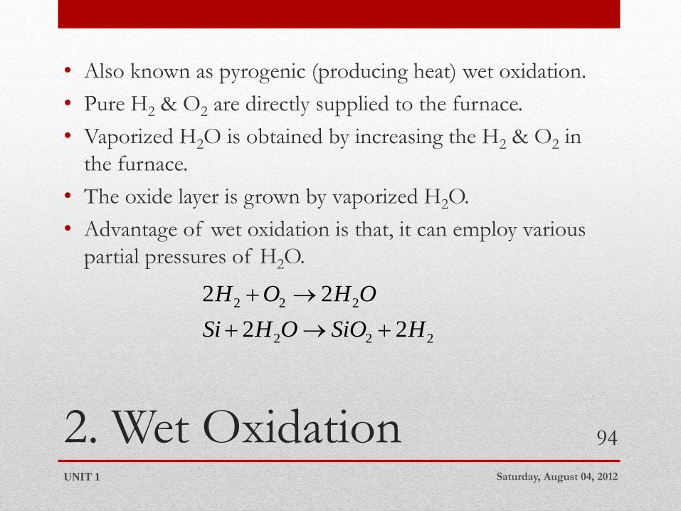
• Also known as pyrogenic (producing heat) wet oxidation.
• Pure H2 & O2 are directly supplied to the furnace.
• Vaporized H2O is obtained by increasing the H2 & O2 in
the furnace.
• The oxide layer is grown by vaporized H2O.
• Advantage of wet oxidation is that, it can employ various
partial pressures of H2O.
Saturday, August 04, 2012 UNIT 1
94
2 2 2
2 2 2
2 2
2 2
H O H O
Si H O SiO H

3. High Pressure
Oxidation
• The oxidation rate can be enhanced at lower temperature by
increasing the pressure of the oxidizing species.
• The increased pressure will allow the oxidizing species to
penetrate the growing oxide layer more rapidly.
• At high partial pressure, the oxidation rate becomes limited
by the reaction rate at the Si-SiO2 interface instead of the
oxidants in SiO2.
• The oxidation rate varies directly with pressure P.
Saturday, August 04, 2012 UNIT 1
95

Cond…
• High pressure oxidation technique has been used mostly on
bipolar devices to increase speed of the devices.
• So for any case, high pressure oxidation can be performed
at lower temperature instead of oxidation at Atmospheric
pressure.
• For example, under 10 atm of steam, the oxidation rate at
8500 C is comparable to that above 12000 C and 1 atm of
steam.
Saturday, August 04, 2012 UNIT 1
96
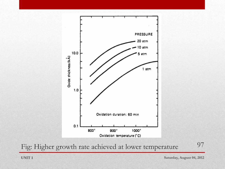
Fig: Higher growth rate achieved at lower temperature
Saturday, August 04, 2012 UNIT 1
97

4. Plasma Oxidation
• Plasma oxidation process offers the possibility of growing
high quality oxides at temperature even lower than those
achieved with the high pressure technique.
• It is low temperature vacuum process.
• The plasma is produced by high frequency discharge or a
DC electron source.
• Place the wafer in a uniform density region of plasma.
• Biasing it positively below the plasma potential.
• Allow it to collect active charged oxygen species.
Saturday, August 04, 2012 UNIT 1
98

Cond…
• The growth rate of oxide increases with increasing
substrate temperature, plasma density and substrate dopant
concentration.
• The quality of oxide grown by this process can be as good
as that of thermally grown SiO2.
• Anodic plasma oxidation can grow thick oxides on the
order of 1µm at lower temperature (< 6000 C) at growth
rate upto about 1µm/h.
Saturday, August 04, 2012 UNIT 1
99

Oxide properties
• There 3 properties of oxides;
1. Masking properties
2. Oxide charges
3. Oxide stress
Saturday, August 04, 2012 UNIT 1
100
1. Masking properties
• SiO2 layer is used as mask.
• During the process of IC fabrication, the temperature of
the Si wafer is very high to derive in dopants into the
silicon.
• These dopants are near the Si surface and occurs because
of the process of ion-implantation & diffusion.
• So, it is very important that dopants should not enter into
the Si wafer and not into SiO2.
• So, the SiO2 layer is responsible for the dopants are blocked
by SiO2 and should enter into Si.
Saturday, August 04, 2012 UNIT 1
101

Cond…
• Usually 0.5 µm to 0.7 µm oxides are used to mask.
• The common impurities used are phosphorus, antimony
and arsenic for n type doping and boron for p type doping.
• All the impurities must have small diffusion coefficients in
oxide so that SiO2 serves as effective mask for them.
Saturday, August 04, 2012 UNIT 1
102

2. Oxide charges
• At the Silicon-Oxide interface, there is a transition region
between crystalline silicon and amorphous silica.
• Various charges and traps are associated with the thermally
oxidized silicon.
• A charge at the interface can induce a charge of the
opposite polarity in the underlying silicon.
• This charge affects the ideal characteristics of the MOS
devices.
• See, figure on next slide.
Saturday, August 04, 2012 UNIT 1
103

Fig: Charges in thermally oxidized silicon Saturday, August 04, 2012 UNIT 1
104

Cond…
• The net number of charges at Si-SiO2 interface is given by:
N=Q/q; where;
• N is net number of charges per unit area (number/cm2) at
Si-SiO2 interface.
• Q is net charge per unit area (Coulombs/cm2) at Si-SiO2
interface.
• q is electric charge in Coulombs.
Saturday, August 04, 2012 UNIT 1
105

Cond…
• There are four kind of oxide charges.
1. Interface trapped charges
2. Fixed oxide charges
3. Mobile ionic charges
4. Oxide trapped charges.
Saturday, August 04, 2012 UNIT 1
106

Cond...
• Interface-trapped charges Qit can interact electrically
with the underlying silicon.
• These charges results from several sources, like structural
defects, metallic impurities or bond-breaking process.
• So, in order to neutralize the Interface-trapped charges Qit,
a low temperature (450 0C)hydrogen anneal is required.
Saturday, August 04, 2012 UNIT 1
107

Cond…
• The fixed oxide charges Qf are located in the oxide
within 30 0A of the Si-SiO2 interface.
• Qf can’t be charged or discharged. It’s density varies from
1010/cm2 to 1012/cm2.
• Qf is related to the oxidation process.
• For electrical measurements Qf can be considered as a
charge sheet at Si-SiO2 interface.
Saturday, August 04, 2012 UNIT 1
108

Cond…
• Mobile ionic charges QM is formed due to the alkali ions
such as Na, K & Li as well as –ve ions and heavy metals.
• The alkali ions are mobile even at room temperature.
• When electric fields are present, density of QM, varies from
1010/cm2 to 1012/cm2 or higher and are related to
processing materials, chemicals ambient or handling.
Saturday, August 04, 2012 UNIT 1
109

Cond…
• Oxide trapped charges Qot may be +ve or –ve due to
holes or electrons trapped in the bulk oxide.
• The charge associated with defects in the SiO2, may occur
from ionizing radiation or higher currents in the oxide.
• It can be annealed out by low temperature.
• Density of Qot, varies from 1009/cm2 to 1013/cm2.
Saturday, August 04, 2012 UNIT 1
110

3. Stress in Oxide Layer
• Stress occurs because of temperature variations during the
oxidation.
• Stress associated with a film is important, because high
stress levels can contribute to wafer warpage, film cracking
and defect formation in the underlying silicon.
• At room temperature stress value is about 3x10⁹ dyne/cm2
is obtained.
• So, stress-free oxidation is usually preferred.
Saturday, August 04, 2012 UNIT 1
111
Defects Induced Due to
Oxidation
• The defects may be introduced in silicon wafer while
oxidation takes place.
• These defects may degrade the performance of integrated
circuits.
• So, care must be taken during the process of oxidation.
• 2 kind of defects occurs basically;
1. Defects due to oxide isolation
2. Staking faults due to oxidation.
Saturday, August 04, 2012 UNIT 1
112
1. Defects due to oxide
isolation
• In VLSI, junctions are usually isolated with oxide-isolation
technique.
• The stress along the edge of oxidizing area may damage the
silicon substrate.
• Due to this stress, the leakage current of nearby or adjacent
devices get increased.
• So in order to prevent defects due to oxide isolation, the
temperature should be sufficiently large (9500 C)during
oxidation.
Saturday, August 04, 2012 UNIT 1
113

2. Staking faults due to
oxidation
• The stacking faults may occur because of thermal oxidation
of silicon.
• These faults are structural defects of the silicon lattice.
• During the thermal oxidation, if the oxidation temperature
is high the oxidant species penetrate silicon at very high
speed.
• So, some of the silicon atoms in the silicon lattice may be
displaced.
• This creates structural defects in the silicon lattice.
Saturday, August 04, 2012 UNIT 1
114

Cond…
• The stacking fault is temperature dependent.
• For higher oxide thickness, shorter stacking faults are
grown, if the oxidation temperature is lower.
• For oxide thickness of 1 µm, stacking fault is completely
suppressed when temperature is below 950 0C.
Saturday, August 04, 2012 UNIT 1
115

Review Questions
1. What is IC’s? Describe the types of IC’s?
2. What are the features of ICs?
3. What are the advantages & disadvantages of ICs?
4. Describe IC fabrication Steps.
5. How pull rate is adjusted during CZ crustal growth?
Explain how dopant incorporation takes place during Cz
crystal growth process?
6. What is single crystal growth? Describe CZ crystal growth
technique.
7. What is the Pull Rate in CZ technique? How the Pull Rate
is controlled during the CZ crystal growth process?
Saturday, August 04, 2012 UNIT 1
116

8. Explain wafer processing techniques used in IC
technology.
9. Why oxidation is done? Explain the chemistry of
oxidation and kinetic of oxide growth.
10. Compare dry and wet process of silicon oxidation.
11. What is High Pressure oxidation? Describe the wafer
processing steps.
12. What are disadvantages of IC`s over discrete circuits?
13. What are monolithic and hybrid ICs.
14. How resistivity of the crystal is measured? A boron-
doped crystal is measured at its seed end with a four-
probe of spacing 1mm. The (V/I) reading is 10 ohms.
What is the resistivity at seed end?
Saturday, August 04, 2012 UNIT 1
117

15. Describe the preparation method for metallurgical grade
silicon (MGS).
16. Describe the preparation method for electronic grade
silicon (EGS).
17. What are seed end and tang end of silicon boule. How
they are obtained.
18. Describe how the shaping of ingot is done?
19. What is the need of wafer etching and polishing? Explain
the process.
20. What are Oxide-Induced defects?
Saturday, August 04, 2012 UNIT 1
118

21. What are the properties of Oxide Layer?
22. Write short note on masking property of oxidation layer.
23. What is oxidation? Explain kinetics behind the oxide
growth.
24. What are linear and digital IC?
25. Explain the process in which CVD reactor is used.
26. Calculate oxide thickness. Also show that,
reduces to for short time and to for long
time, where x = oxide thickness
Saturday, August 04, 2012 UNIT 1
119
1/2
21 1
/ 2 / 4
x t
A A B
( )B
x tA
( )x B t

27. Discuss different steps in preparing wafers from the raw
silicon.
28. Explain the application of SiO2 layer in IC fabrication.
29. Show that to grow an oxide layer of thickness x, a
thickness of 0.44x of silicon is consumed.
30. State Moore’s law.
31. Why SiO2 is an important component in electronics?
32. A silicon ingot with 0.5x10¹⁶ boron atoms/cm3 is to be
grown by Cz method. What should be the concentration
of boron in the melt to obtain the required doping
concentration? The segregation coefficient of the boron
is 0.8.
Saturday, August 04, 2012 UNIT 1
120

References
1. VLSI Technology/S. M. SZE/2nd Ed./TMH
2. VLSI Fabrication Principles Silicon and Gallium
Arsenide/Sorab K. Gandhi/2nd Ed./Wiley
3. The Science and Engineering of Microelectronic
Fabrication/S. A. Campbell/2nd Ed./Oxford
4. Silicon VLSI Technology – Fundamentals, Practice and
Modeling/J. D. Plummer, M. D. Deal & P. D. Griffin/1st
Ed./Pearson
5. Semiconductor Devices: Physics & Technology/2nd
Ed./S. M. Sze/Wiley
Saturday, August 04, 2012 UNIT 1
121