Embed Size (px)
Citation preview
1
Unit – I
LASERS
1.1 Introduction :
The word “LASER” is an acronym for “Light Amplification by Stimulated Emission
of Radiation”. Albert Einstein in 1917 theoretically proved that the process of stimulated
emission must exist. But only in 1954, a group of scientists at Columbia University head by
Charles H.Townes operated a microwave device for “Microwave Amplification by
Stimulated Emission of Radiation (MASTER)”. In 1960, T.H.Maiman of the Hughes
Research Laboratories first achieved laser action at optical frequency in Ruby. Since 1960 the
development of lasers has been extremely rapid.
1.2 Spontaneous and Stimulated Emission of Radiation :
If the radiation interacts with atoms in the lower energy state, say E1, the atoms absorb
the energy and get excited to the higher energy state E2 by a process called stimulated
absorption. Instead if the radiation interacts with atoms which are already in the excited state
E2, then de-excitation of those atoms to the lower energy state E1 occurs with emission of
photons of energy hv . This process is called stimulated emission. Yet another emission
process called spontaneous emission is also possible wherein atoms in the excited state drop
to the lower energy state after they have stayed in the excited state for a short duration of time
called their life time. During this process also photons of energy )( 12 EEhv are emitted.
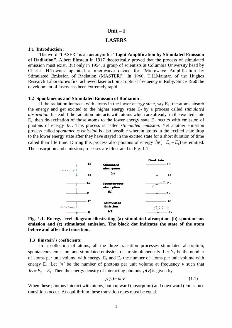
The absorption and emission processes are illustrated in Fig. 1.1.
Fig. 1.1. Energy level diagram illustrating (a) stimulated absorption (b) spontaneous
emission and (c) stimulated emission. The black dot indicates the state of the atom
before and after the transition.
1.3 Einstein’s coefficients
In a collection of atoms, all the three transition processes–stimulated absorption,
spontaneous emission, and stimulated emission–occur simultaneously. Let N1 be the number
of atoms per unit volume with energy. E1 and E2 the number of atoms per unit volume with
energy E2. Let ‘n’ be the number of photons per unit volume at frequency v such that
12 EEhv . Then the energy density of interacting photons )(v is given by
nhvv )( (1.1)
When these photons interact with atoms, both upward (absorption) and downward (emission)
transitions occur. At equilibrium these transition rates must be equal.
2
Upward transition
Stimulated absorption rate depends on the number of atoms available in the lower
energy state for absorption of these photons as well as the energy density of interacting
radiation.
i.e., Stimulated absorption rate 1N
)(v
= 121 )( BvN
Where the constant of proportionality 12B is the Einstein coefficient of stimulated absorption.
Downward transition
Once the atoms are excited by stimulated absorption, they ‘stay’ in the excited state for
a short duration of time called the life time of the excited state. After their life time they
move to their lower energy level spontaneously emitting photons. This spontaneous emission
rate depends on the number of atoms in the excited energy state.
i.e. Spontaneous emission rate 2N
)(v
= 212 )( BvN
where the constant of proportionality 21B is the Einstein coefficient of stimulated emission.
During stimulated emission, the interacting photon called the stimulating photon and
the photon due to stimulated emission are in phase with each other. Please note that during
stimulated absorption, the photon density decreases whereas during stimulated emission it
increases.
For a system in equilibrium, the upward and downward transition rates must be equal
and hence we have
212212121 )()( ANBvNBvN (1.2)
hence
212121
212)(BNBN
ANv
(1.3)
or
1
/)(
2
1
21
12
2121
N
N
B
B
BAv (1.4)
The population of the various energy levels of a system in thermal equilibrium is given by
Boltzmann distribution law.
kT
ENogN i
ii exp (1.5)
Where iN is the population density of the energy level iE , 0N is the population density of the
ground state at temperature T, ig is the degeneracy of the ith
level and k is the Boltzmann
constant (=1.38 x 10⁻²³
joule/K). (The concept of degeneracy occurs since more than one
level have the same energy).
3
Hence kTENogN /1
exp11
kTENogN /2
exp22
kT
EE
g
g
N
N )12
(exp
2
1
2
1
kT
hv
g
g
exp
2
1 (1.6)
Substituting equation (1.6) in equation (1.4)
1exp
21
12
2
1
21/
21)(
kT
hv
B
B
g
g
BAv
(1.7)
From Planck’s low of black body radiation, the radiation density is given by
1exp
1
3
38)(
kT
hvc
hvv
(1.8)
comparing equations (1.7) and (1.8)
1
21
12
2
1
B
B
g
g
212121 BgBg (1.9)
and
3
38
21
21
c
hv
B
A (1.10)
Equations (1.9) and (1.10) are referred to as the Einstein relations.
The ratio of spontaneous emission rate to the stimulated emission rate is given by
221 )(/
21)(
2
212 BvABvN
ANR
from equation (1.7)
1exp
21)(
21
kT
hv
Bv
AR
(1.11)
From eq.(1.11) we understand that to make R smaller, )(v the energy density of interacting
radiation has to be made larger. Let us consider the ratio of stimulated emission rate to
stimulated absorption rate.
12)(
1
21)(
2
rateabsorptionStimulated
rateemissionStimulated
BvN
BvN
= )degeneracygnoring(/ 122112 iBBasNN
At thermal equilibrium 1/ 12 NN
4
Thus at thermal equilibrium stimulated absorption predominates over stimulated emission.
Instead if we create a situation that ,12 NN stimulated emission will predominate over
stimulated absorption. If stimulated emission predominates the photon density increases and
Light Amplification by Stimulated Emission of Radiation (LASER) occurs. Therefore, in
order to achieve more stimulated emission, population of the excited state (N2) should be
made larger than the population of the lower state (N1) and this condition is called population
inversion. Hence, if we wish to amplify a beam of light by stimulated emission then we must
(i) create population inversion and
(ii) increase the energy density of interacting radiation
1.4 Amplification of light :
Let us consider light of intensity 0I entering a medium of length x. The intensity of
light leaving the medium on the other side under thermal equilibrium condition is given by
Beer’s law
)(exp)( 0 xIxI (1.12)
where is the absorption coefficient of the medium. Stimulated absorption results in fall in
intensity of light. If we can create population inversion in the medium, stimulated emission
will predominate over stimulated absorption and hence the light passing through the medium
undergoes amplification instead of attenuation.
)(exp)( 0 xIxI (1.13)
Where is the gain (i.e. amplification) coefficient. Thus when the medium is under the
condition of population inversion, the density of photons (light intensity) passing through the
medium increases.
1.5 Gain coefficient
Let n be the number of photons inside the medium at any instant under the condition
of amplification. Then (dn/dt) gives the rate at which photon density increases. This is
nothing but the difference in stimulated emission rate and stimulated absorption rate
(assuming that spontaneous emission rate is negligible).
i.e. 112221 NvBNvB
dt
dn
Substituting for 21B from equation (11.9)
112
1
2221 NvB
g
gNvB
dt
dn
=211
1
22 )( BvN
g
gN
(1.14)
Intensity of light is given by
nhvcI where c is velocity of light.
hvcdx
dn
dx
dI
hvcdx
dx
dIdn
1.
hvcdt
dx
dx
dI
dt
dn 1
5
c
dt
dxas
hvcdx
dI 1
From equation (1.13)
).(exp0 xIdx
dI
= )(xI
Substituting in the above equation
nchv
nhvchv
xdt
dn
11)(1
(1.15)
Comparing equations (11.14) and (11.15)
c
hvBN
g
gN
nc
vBN
g
gN 211
1
22211
1
22
)(
(1.16)
This process causing light amplification by stimulated emission of radiation is the underlying
basis for laser action. This is possible (i.e., is positive) only when N2 is greater than 1
1
2 Ng
g
i.e. only when population inversion is achieved.
1.5 Population Inversion
The population inversion condition required for light amplification is a non-
equilibrium distribution of atoms among the various energy levels of the atomic system.
Boltzmann distribution law specifies what fraction of atoms are found in any particulars
energy state for any given equilibrium temperature. If 0N is the number of atoms in the
ground state, iN is the number of atoms in the excited state of energy iE measured relative to
the ground state, then (ignoring degeneracy).
kT
E
N
N iexp0
1
(1.17)
Where T is the absolute temperature in degree Kelvin; and k = 1.38 x 10⁻²³
joule/K .
Since the right hand side of the above equation is exponential of a negative quantity,
maximum possible value attainable is 1. That happens when .iEkT Even then at this
extreme (impossible ) case, iN can be equal to 0N but it will never exceed 0N . Hence from
this it is very obvious that by feeding energy required for exciting the atoms from lower
energy level to the higher energy level, higher level can never be made more populated than
the lower level. i.e. by direct pumping population inversion is not possible. Then how is
population inversion achieved?
From the above we have understood that if two energy levels are involved, by direct
pumping the higher level cannot be made more populated than the lower level. The
restrictions imposed on a two level scheme have been overcome in three and four level
schemes by pumping atoms in the active medium indirectly to the upper state of transition
involving more than two energy levels.
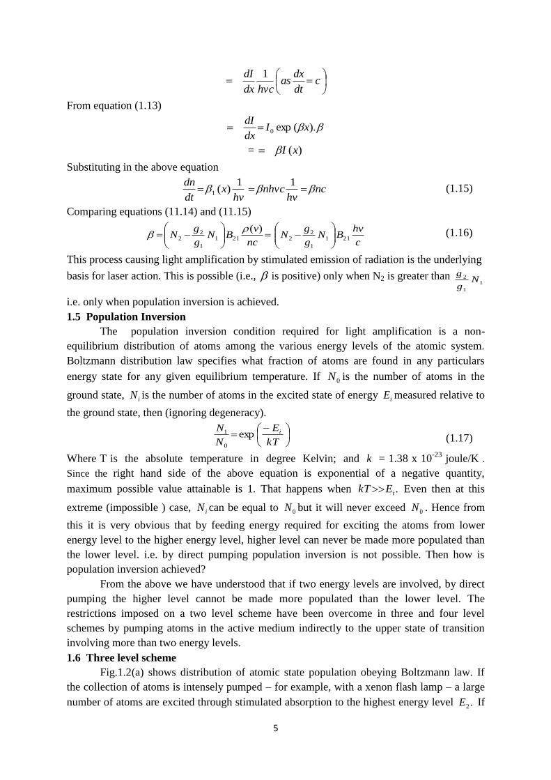
1.6 Three level scheme
Fig.1.2(a) shows distribution of atomic state population obeying Boltzmann law. If
the collection of atoms is intensely pumped – for example, with a xenon flash lamp – a large
number of atoms are excited through stimulated absorption to the highest energy level .2E If
6
the level 2E has very short lifetime, the atoms decay fast to level .1E If the level
1E has
relatively longer lifetime (a state known as metastable) atoms tend to accumulate at 1E . With
intense pumping from 0E to 2E , because of rapid decay to
1E , it is possible to bring in non-
equilibrium distribution of atoms viz 1E more populated than 0E and laser transition takes
place between level 1E (called upper laser level) and level 0E (called lower laser level) as
shown in Fig. 1.2(b). Since ground level 0E happens to be the lower laser level, more than
one-half of the ground state atoms must be pumped to the upper state to achieve population
inversion )( 01 NN . Therefore, three level pumping schemes generally require very high
pump powers. If pumping continues when the condition )( 01 NN is reached, stimulated
emission rate exceeds stimulated absorption rate. This immediately depopulates the upper
laser level and populate the lower laser level. Hence it is not possible to continuously
maintain the upper laser level more populated than the lower laser level, Such a system
therefore works in pulsed mode only. The Ruby laser is the best example for a three level
system.
Fig.1.2 Population of energy levels by pumping in a three level system
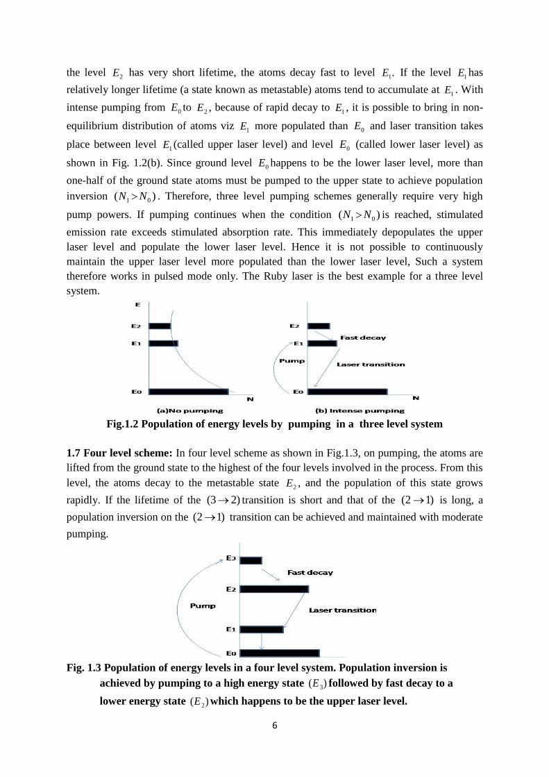
1.7 Four level scheme: In four level scheme as shown in Fig.1.3, on pumping, the atoms are
lifted from the ground state to the highest of the four levels involved in the process. From this
level, the atoms decay to the metastable state 2E , and the population of this state grows
rapidly. If the lifetime of the )23( transition is short and that of the )12( is long, a
population inversion on the )12( transition can be achieved and maintained with moderate
pumping.
Fig. 1.3 Population of energy levels in a four level system. Population inversion is
achieved by pumping to a high energy state )( 3E followed by fast decay to a
lower energy state )( 2E which happens to be the upper laser level.
7
Since ground level is not the lower laser level there is no need to pump more then one-half of
the population to the higher level. Since in this scheme level is the 1E is the lower laser level,
it is relatively easier to maintain population inversion between levels 12 and EE
continuously with moderate pumping and get continuous wave (CW) output. For this to
happen )01( transition must be very fast. If this transition is relatively slow, even four level
laser will work in pulsed mode only. NeHe laser is a good example for a four level laser
working in CW mode while 2N laser is an example for pulsed mode of operation.
1.8 Pumping mechanisms – creation of population inversion
There are different mechanisms applied to pump the atoms of the active medium to
higher energy states to create population inversion. They are
(i) optical pumping
(ii) electric discharge
(iii) chemical reaction
(iv) injection current etc.
Optical pumping is the very first mechanism applied to Ruby laser. Solid state lasers are
optically pumped using Xenon flash lamps. Since these materials have very broad band
absorption, sufficient amount of energy is absorbed from the emission band of flash lamp and
population inversion created. Recently flash lamps are being replaced by laser diodes thus
making systems more efficient and reliable. Examples of optically pumped lasers are Ruby,
,:,: GlassNdYAGNd Dye, etc., Since gas lasers have very narrow absorption band, pumping
them using any flash lamp is not possible. In most of the cases inversion is created by means
of electric discharge. Examples of such systems are ,NeHe Argon ion, Carbon dioxide
etc.
Chemical reaction may also result in excitation and hence creation of population inversion
in few systems. Examples of such systems are FDFH , and atomic iodine lasers.
In semiconductor lasers, the injection current through the junction results in creation of
population inversion among charge carriers.
1.9 Resonator
Resonator mirrors are generally coated with multilayer dielectric materials to reduce
the absorption loss in the mirrors. Moreover these resonators act as frequency selectors and
also give rise to directionality to the output beam. Since the resonator mirrors provide
feedback to the photons amplified by the achre medium.
1.10 Modes of a rectangular cavity
The electric field of an e.m wave satisfies the equation 2
2
2
2 1
rt
E
CE
(1.18)
where c is the velocity of light. The simplest plane wave solution of Eq.(1.18) is
wt)(k.r(iexpEt)(r,E 0 (1.19)
Where 0E is the amplitude and k the wave vector. The complete solution with real spatial
parts is
zksin y ksin Xcosk(t)E(t)E zyxoxx
zksin y kcos Xsink(t)E(t)E zyxoyy
8
zk cosy ksin Xksin(t)E(t)E zyxozz
with 222
2 zyx kkkk (1.20)
Eq. (3) have to satisfy Maxwell’s equation 0. E
0 (t)Ek(t)Ek (t)Ek ozzoyyoxx
0 (t)k.E(ie)
Hence k is perpendicular to E. The waves have to satisfy a boundary condition at the walls.
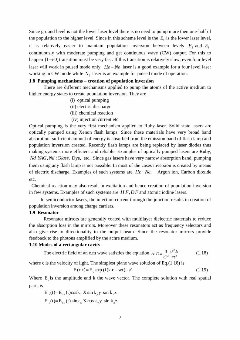
(i) the tangential components of the field must vanish at the walls. For simplicity, let us
assume the cavity to be a cube of length L as shown in Fig. 1.4.
Fig.1.4 Cubic cavity
As )(x tE must vanish at x = 0 and y = L.
y = 0 and z = L.
L
qk
L
nk zy
(1.21a)
Similarly )(x tE must vanish at x = 0 and x = L.
L
mkx
(1.21b)
Where m, n, q = 0, 1, 2. The boundary conditions force the wave vector components to take
discrete values specified by m, n, q. Each set of integers (m,n,q) defines a mode of vibration.
These modes are known as Transverse Electromagnetic modes and are denoted by TEM mnq
where m and n are tranverse indices and q is the longitudinal index. Each mode has a
characteristic distribution of amplitude and phase. This distribution in a plane perpendicular
to the resonator axis is described by transverse indices m,n. A given combination of m, n
defines a transverse mode regardless of the value of q. This is denoted as TEM mnq mode. For
each combination of mn, there are modes different values of q. These are called longitudinal
or axial modes. Thus there is an infinite number of resonant frequencies corresponding to
different values of m, n, q. Any excitation of the electro magnetic field observed in the
resonator can be expressed as a linear combination of these modes.
Number of modes per unit volume
We can plot the wave vectors k in a three dimensional space with the components kx,
ky, kz as shown in Fig.1.5. This is called k space. The allowed values of k are given by
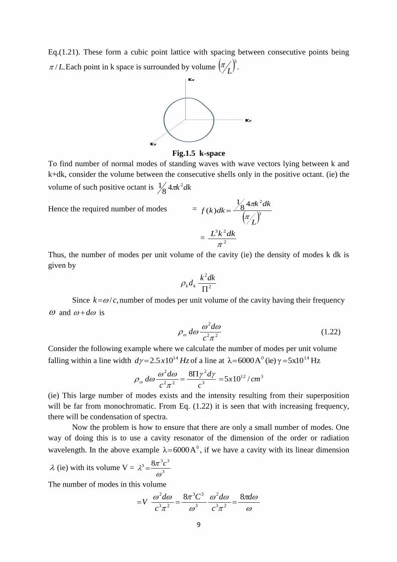
9
Eq.(1.21). These form a cubic point lattice with spacing between consecutive points being
./ L Each point in k space is surrounded by volume .3
L
Fig.1.5 k-space
To find number of normal modes of standing waves with wave vectors lying between k and
k+dk, consider the volume between the consecutive shells only in the positive octant. (ie) the
volume of such positive octant is dkk 248
1
Hence the required number of modes =
324
81
)(
L
dkkdkkf
= 2
23
dkkL
Thus, the number of modes per unit volume of the cavity (ie) the density of modes k dk is
given by
2
2
dkkdkk
Since ,/ck number of modes per unit volume of the cavity having their frequency
and d is
22
2
c
dd (1.22)
Consider the following example where we calculate the number of modes per unit volume
falling within a line width Hzxd 14105.2 of a line at Hz5x10γ(ie)A6000λ 140
312
3
2
22
2
/1058
cmxc
d
c
dd
(ie) This large number of modes exists and the intensity resulting from their superposition
will be far from monochromatic. From Eq. (1.22) it is seen that with increasing frequency,
there will be condensation of spectra.
Now the problem is how to ensure that there are only a small number of modes. One
way of doing this is to use a cavity resonator of the dimension of the order or radiation
wavelength. In the above example 0A6000λ , if we have a cavity with its linear dimension
(ie) with its volume V = 3
333 8
c
The number of modes in this volume
d
c
dC
c
dV
8823
2
3
33
23
2
10
(ie) The number of modes will go on decreasing with increasing frequency. Construction of
such a resonator is not practical. Moreover, such a small volume of active medium is useless
because it does not yield output power. To solve the above difficulties, Schawlow and
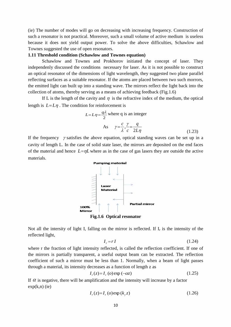
Townes suggested the use of open resonators.
1.11 Threshold condition (Schawlow and Townes equation)
Schawlow and Townes and Prokhorov initiated the concept of laser. They
independenly discussed the conditions necessary for laser. As it is not possible to construct
an optical resonator of the dimensions of light wavelength, they suggested two plane parallel
reflecting surfaces as a suitable resonator. If the atoms are placed between two such morrors,
the emitted light can built up into a standing wave. The mirrors reflect the light back into the
collection of atoms, thereby serving as a means of achieving feedback (Fig.1.6)
If L is the length of the cavity and is the refractive index of the medium, the optical
length is LL . The condition for reinforcement is
2
qLL where q is an integer
As
L
q
c
c
2,
(1.23)
If the frequency satisfies the above equation, optical standing waves can be set up in a
cavity of length L. In the case of solid state laser, the mirrors are deposited on the end faces
of the material and hence LL where as in the case of gas lasers they are outside the active
materials.
Fig.1.6 Optical resonator
Not all the intersity of light I, falling on the mirror is reflected. If Ir is the intensity of the
reflected light,
IrI r (1.24)
where r the fraction of light intensity reflected, is called the reflection coefficient. If one of
the mirrors is partially transparent, a useful output beam can be extracted. The reflection
coefficient of such a mirror must be less than 1. Normally, when a beam of light passes
through a material, its intensity decreases as a function of length z as
)(exp)()( zoIzI rr (1.25)
If is negative, there will be amplification and the intensity will increase by a factor
exp(k,n) (ie)
)(exp)()( zkoIzI rr (1.26)
11
Where K is called unsaturated gain coefficient. It determines the gain that exists
before amplification. Let r1 r2 be the reflection coefficients of the two mirrors. Then the
energy of the wave in one complete passage back and forth will diminish by a factor r1 r2 (ie)
2
21
err
211
2
1rrn (1.27)
where is positive and it is measure of loss of light in a single passage. (ie) After each
passage, intensity will be diminished by e (ie) I reduces to
Ie . Assuming that reflection
losses are the only losses present in the cavity, the intensity in each passage change from I to
l exp Lk. For oscillations to be sustained in a laser, the amplification must be sufficient
to compensate for the energy lost.For oscillations to build up
exp LkorLk 1 (1.28)
Hence threshold will be reached when
Lk (1.29)
A laser with length L and given mirror reflectivity will operate only if
Lk /3 (1.30)
)(12
2
1
2
1
21
2
2
2
gNN
g
g
g
Ahck
(1.31)
where )(g accounts for the distribution in the line. Thus in the case of a line profile
dominated by Lorentz broadening, the gain coefficient is given by
422)(
1
21)(
1
2
2
1
2
1
121
22
N
N
g
g
g
Ngck L (1.31)
The maximum value of the gain coefficient is obtained at
12
)(1
2
2
1
2
1
12
220
N
N
g
g
g
Ngck L
(11)
21
21
1A
(ie) The maximum gain decreases as the square of the transition frequency increases. This
explains why laser oscillations are easier to achieve in the infrared region than in the visible
and ultra violet regions.
For lasers to operate
L
gNNg
g
g
Agc
)(12
2
1
2
1
122
22
(1.32)
The laser will operate in the frequency interval in which the above condition is satisfied.
At the threshold, the condition becomes,
122
22
2
112
2
1
AgLc
gNN
g
g
(1.33)
12
For non-degenerate states
)(
12
22
2
12
gALcNN (1.34)
This value of population inversion is known as the critical inversion. The above formula
suggests that for the onset of oscillations, and L must be properly adjusted.
Eqn (1.34) can be expressed in a different form. Let P be the number of photons travelling
back and forth in a laser. The number of photons after m passenger will be
gmePP
(1.35)
It L is the time taken by a photon for a single passage, the time taken for m passage will be
)Lmt
)/exp( LtPP (1.36)
The average life time p of a photon is the time by which P is rreduced to P /e
c
L
c
LL
Lp
||
pc
L
|
(1.37)
Using this, Eq. (1.34) can be expressed in the form
)(12
22
21
2
12
gALc
LNN
L
A
|
21
1
Since, LL '
)(23
21
2
12
gcNN
p
(1.38)
As )(g =
2 , the above equation becomes
23
21
2
122 pc
NN (1.39)
This equation is known as Schawlow–Townes condition for laser oscillations. The population
difference required to make laser oscillations depends on the two life times, the spontaneous
life time of the upper energy level and the effective decay time of the cavity
.
Rate equations : Two level system:
Consider the time evolution of the population of a two level energy system in the
presence of a monochromatic electro magnetic wave. If the frequency of the
electromagnetic, wave is equal to the transition frequency 21 , some of the atoms will absorb
13
energy and come to the upper level. Let N1, N2 be the populations of the two levels per unit
volume and N0 the total population which is constant (ie)
021 NNN (1.40)
Let NNN 21 (1.41)
Combining Eqs (1.40)and (1.41) we get
21
NNN
2
2
NNN
(1.42)
Excited atoms come to the lower level by spontaneous and stimulated emission. Apart from
radiative transition, atoms can make nonradiative transitions by giving their excess energy to
the surrounding atoms in the case of a gas or to the lattice in the case of a solid. The
probability of spontaneous transition is represented by )(1sp
sp
A
Similarly the
probability of non radiative transition is represented by .1
nrnrsp and are the
spontaneous emission decay time and life time of non radiative transition is represented by
.1nr nrsp and are the spontaneous emission decay time and life time of non radiative
process respectively.
The overall time decay is given by
nrsp
111 (1.43)
The rate of change of the population of the upper level is given by
2
22121121122 )()(
NNBNB
dt
dN where is the density of radiation 2112 BB
2
2112 )(N
NB
Where B12, B21 are Einstein’s coefficients. The second term on the RHS represents both
spontaneous and non radiative transitions.
In the steady state, 0/2 dtdN
2)( 2
2112
NNNNB
NNNB )(2(ie) 2112
NNBN )(2| 2112
)(21 2112B
NN
(1.44)
This equation shows that the population difference between the two levels in a steady state
depends on the decay time of the upper level and on the density of incident radiation )( 21
)( 2112 B is the probability per unit time that the atoms are excited to the upper level and is
called the pumping rate. We represent it by .
21
NN (1.45)
14
We see that whatever the value of , N is always positive and hence inversion is not
possible.
2/)(0,If 021 NNNieN
Hence a two level system is not suitable for optical pumping. The pump power absorbed by
the material per unit volume, to maintain a given population difference N is
)(21
)()(
2121
211221211221
B
NBNB
dv
d
If ,1)( 2112 B then
2
21 N
dv
d (1.46)
Thus the pump power also depends upon the decay time
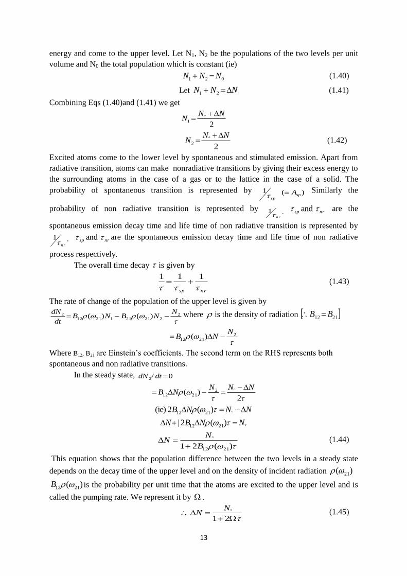
Rate equation – Three level system:
Let us now consider a three level system as shown in Fig. 1.7. Of all the atoms
pumped into level 3 from level 1, some go back to level 1 by spontaneous and stimulated
emissions and some to level 2 by radiative and non radiative processes.
Fig.1.7 Three level system
The rate equations in the steady state are
0)()( 32331331313311313 SNANBNBN
dt
dN (1.47a)
where
i. the 1st term represents number of atoms arriving at the level 3 per unit time per unit
volume due to induced or stimulated absorption.
ii. 2nd
term represents the number of stimulated emissions
iii. 3rd
term represents is the number of spontaneous emissions.
iv. 4th
term represents transition to the level 2 due to radiative and no radiative processes
S32 is the probability of transitions.
0)( 323313313133232 SNANBNSN
dt
dN (1.47b)
Here the last two terms represent induced transitions between levels 1 and 2 due to the
presence of laser radiation.
0)()()()( 211213113121231122313311331 BNBNANBNANBN
dt
dN
(1.47c)
3210 NNNN
From eqs. 1.47(a) (b) (c), we see that
15
0321
dt
dN
dt
dN
dt
dN (1.48)
Which is consistent with Eq.(1.47).
Solving these equations for ,findingandand 1221 NNNN We get
32313113
2131123113323113212112
32313113
323113
12
)(
)()()()(2
)(
)(
SAB
ABBSBAB
SAB
SBN
NN
(1.49)
From Eq. (1.47a), number of atoms arriving per unit time at the
Level 2 is 32313113
3231131323
)(
)(
SAB
SBNSN
Hence, the probability that an atom arrives at level 2 is
32313113
323113
)(
)(
SAB
SB
Using this in Eq. (1.49)
32313113
2131123113323113212112
2112
)(
)()()()(2
)(
SAB
ABBSBAB
ANNN
For population inversion (ie) 12 NN is positive, it is necessary that 21A
21
32313113
323113
)(
)((ie) A
SAB
SB
Using a beam of suitable intensity, it is possible to produce the required population inversion.
The quantity 21inv A is called the inversion threshold pumping rate.
1.12 Types of lasers:
The types of laser considered are.
(a) Solid state lasers : For eg. Ruby, Nd: YAG, Nd: glass;
(b) Gas lasers : For eg. He-Ne, Argon ion, and CO2
(c) Liquid lasers : for eg, dyes, chemical lasers
(d) Excimer lasers ;
(e) Semiconductor Lasers
These laser systems are in widespread use today for different applications.
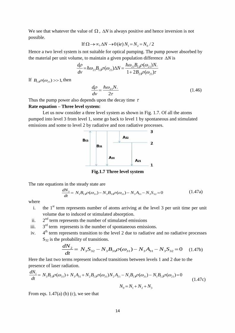
(a) Ruby Laser The first laser to be operated successfully was the ruby laser which was
fabricated by Maiman in 1960.
It consists of a ruby cylindrical rod whose ends are optically flat and accurately
parallel is shown in Fig.1.8. One end is fully silvered and the other is only partially silvered.
The road is surrounded by a glass tube. The glass tube is surrounded by a helical xenon flash
tube which acts as the optical pumping system. The ruby rod is a crystal of aluminium oxide
)( 32OAI doped with 0.05% chromium oxide )( 32OCr , so that some of the aluminium atoms in
the crystal lattice are replaced by 3Cr ions. The energy level diagram of these chromium ions
is shown in Fig. 1.9. The Cr ions are excited from level 1E to level 3E by the absorption of
light of wave length 550 nm from the xenon flash tube. The excited ions quickly undergo
non radiative transitions with a transfer of energy to the lattic thermal motion, to the level .2E
16
Fig.1.8 Ruby laser
The level is a metastable state with a life time of about 3103 x sec (usual atomic lifetime are
= 810sec). Now the population of the .2E level becomes greater than that of the 1E level.
Thus “Population inversion” is achieved.
Fig. 1.9 Energy level diagram of 3Cr ions in ruby
Some photons are produced by spontaneous transition from 2E to 1E and have a wave length
of 694.3 nm (ruby rod). The ends of the ruby rod act as reflecting mirrors. Therefore,
photons that are not moving parallel to the ruby rod escape from the side, but those moving
parallel to it are reflected back and forth. These stimulate the emission of similar other
photons. The chain reaction quickly develops a beam of photons all moving parallel to the
rod, which is monochromatic and is coherent. When the beam develops sufficient intensity, it
emerges through the partially silvered end. Once all the chromium ions in the metastable
level have returned to ground level, the laser action stops. It is then necessary to send one
more flash of pumping radiation through the rod. Thus the ruby laser operates only in pulses.
The output of a pulsed ruby laser, if examined with a photocell and on oscillograph, is
found to consists of a series of pulses of duration of a microsecond or less. Duration of an
individual spike is of the order of 0.1 – 1 s ; the time interval between two adjacent spikes
is about – 1-10 s ; the power of each spike is of the order of 54 1010 W. Such spikes were
first observed in expts with ruby by Collins et al.
(b) Neodymium based Lasers
The Nd : YAG laser (YAG stand for Yttrium Aluminium Garnet which is 1253 OAIY )
and the Nd:glass laser are two very important solid state laser systems in which the energy
17
levels of the neodymium ion take part in laser emission. They both correspond to a four level
laser.Using neodymium ions in a YAG (or) glass host has specific advantages and
applications.
(i) Since glass has an amorphous structure the fluorescent linewidth of emission
is very large leading to a high value of the laser threshold. On the other hand YAG is a
crystalline material and the corresponding linewidth is much smaller which implies much
lower theresholds for laser oscillation.
(ii) The larger linewidth of the glass host than the YAG host can be made use of
in the production of ultra short pulses using mode locking. The pulsewidth obtainable by
mode locking is the inverse of the oscillating linewidth.
(iii) The larger linewidth in glass leads to a smaller amplification coefficient and
thus the capability of storing a larger amount of energy before the occurrence of saturation.
(iv) As compared to YAG, glass has a much lower thermal conductivity which
may lead to induced birefringence and optical distortion.
(v) Glass does not absorb the laser emission.
(vi) Glass materials are optically homogeneous and lend themselves for doping in
high concentration of impurities.
From the above discussion, for continuous or very high pulse repetition rate operation, the
Nd: YAG laser will be preferred over Nd:glass. On the other hand for high energy pulsed
operation, Nd:glass lasers may be preferred.
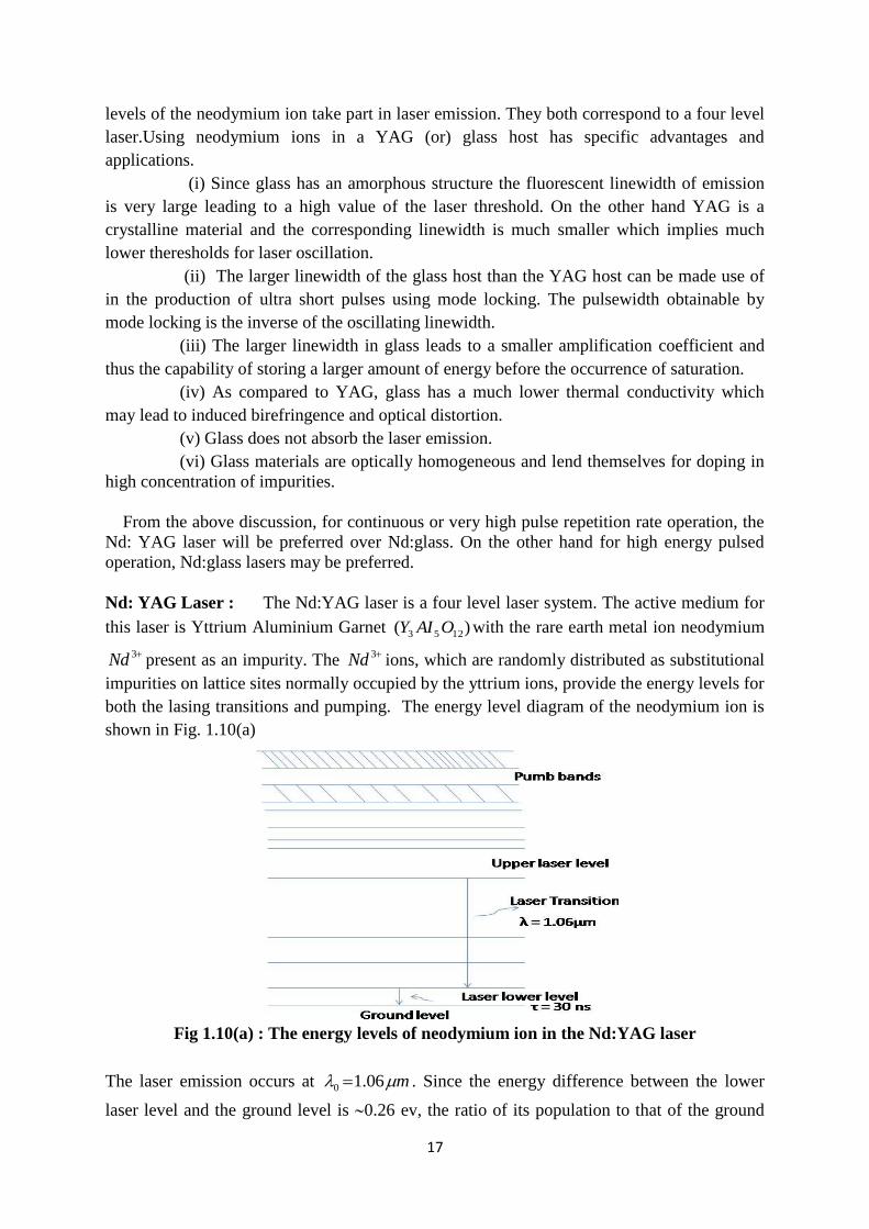
Nd: YAG Laser : The Nd:YAG laser is a four level laser system. The active medium for
this laser is Yttrium Aluminium Garnet )( 1253 OAIY with the rare earth metal ion neodymium
3Nd present as an impurity. The 3Nd ions, which are randomly distributed as substitutional
impurities on lattice sites normally occupied by the yttrium ions, provide the energy levels for
both the lasing transitions and pumping. The energy level diagram of the neodymium ion is
shown in Fig. 1.10(a)
Fig 1.10(a) : The energy levels of neodymium ion in the Nd:YAG laser
The laser emission occurs at m 06.10 . Since the energy difference between the lower
laser level and the ground level is 0.26 ev, the ratio of its population to that of the ground
18
state at room temperature (T = 300 K) is .19 ee TEK Thus the lower laser level is
almost unpopulated and hence inversion is easy to achieve.
The main pump bands for excitation of the neodymium ions are in the 0.81 μm and
0.75 μm wave length region and pumping is done using arc lamps (e.g. Krypton arc lamp).
Typical neodymium ion concentrations used are v1.2 x 1011
Hz which corresponds to
4.5Ao. Already we know that the Nd: YAG laser has a much lower threshold of oscillation
than a ruby laser.
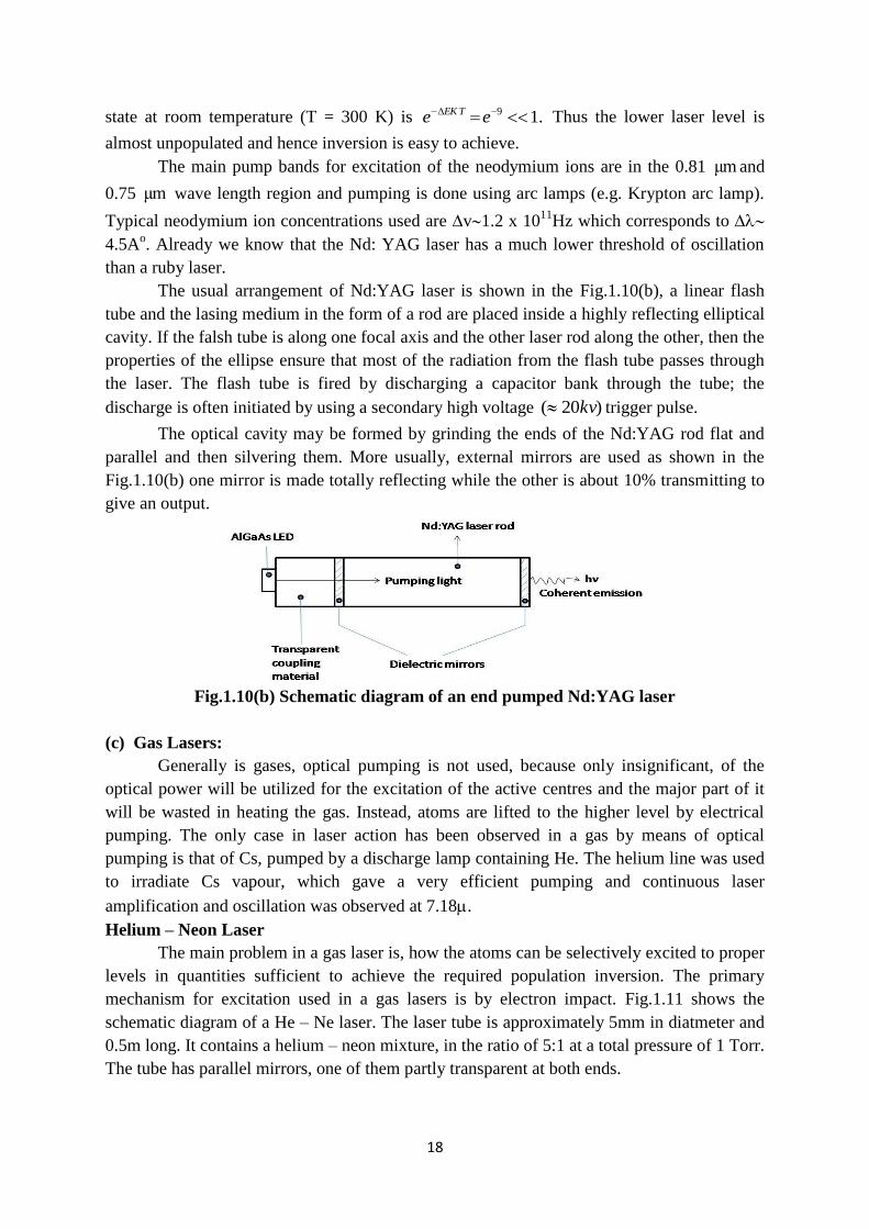
The usual arrangement of Nd:YAG laser is shown in the Fig.1.10(b), a linear flash
tube and the lasing medium in the form of a rod are placed inside a highly reflecting elliptical
cavity. If the falsh tube is along one focal axis and the other laser rod along the other, then the
properties of the ellipse ensure that most of the radiation from the flash tube passes through
the laser. The flash tube is fired by discharging a capacitor bank through the tube; the
discharge is often initiated by using a secondary high voltage )20( kv trigger pulse.
The optical cavity may be formed by grinding the ends of the Nd:YAG rod flat and
parallel and then silvering them. More usually, external mirrors are used as shown in the
Fig.1.10(b) one mirror is made totally reflecting while the other is about 10% transmitting to
give an output.
Fig.1.10(b) Schematic diagram of an end pumped Nd:YAG laser
(c) Gas Lasers:
Generally is gases, optical pumping is not used, because only insignificant, of the
optical power will be utilized for the excitation of the active centres and the major part of it
will be wasted in heating the gas. Instead, atoms are lifted to the higher level by electrical
pumping. The only case in laser action has been observed in a gas by means of optical
pumping is that of Cs, pumped by a discharge lamp containing He. The helium line was used
to irradiate Cs vapour, which gave a very efficient pumping and continuous laser
amplification and oscillation was observed at 7.18.
Helium – Neon Laser
The main problem in a gas laser is, how the atoms can be selectively excited to proper
levels in quantities sufficient to achieve the required population inversion. The primary
mechanism for excitation used in a gas lasers is by electron impact. Fig.1.11 shows the
schematic diagram of a He – Ne laser. The laser tube is approximately 5mm in diatmeter and
0.5m long. It contains a helium – neon mixture, in the ratio of 5:1 at a total pressure of 1 Torr.
The tube has parallel mirrors, one of them partly transparent at both ends.
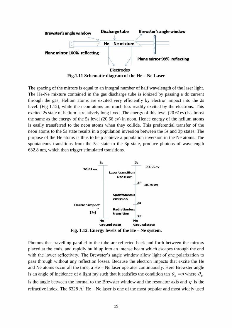
19
Fig.1.11 Schematic diagram of the He – Ne Laser
The spacing of the mirrors is equal to an integral number of half wavelength of the laser light.
The He-Ne mixture contained in the gas discharge tube is ionized by passing a dc current
through the gas. Helium atoms are excited very efficiently by electron impact into the 2s
level. (Fig 1.12), while the neon atoms are much less readily excited by the electrons. This
excited 2s state of helium is relatively long lived. The energy of this level (20.61ev) is almost
the same as the energy of the 5s level (20.66 ev) in neon. Hence energy of the helium atoms
is easily transferred to the neon atoms when they collide. This preferential transfer of the
neon atoms to the 5s state results in a population inversion between the 5s and 3p states. The
purpose of the He atoms is thus to help achieve a population inversion in the Ne atoms. The
spontaneous transitions from the 5st state to the 3p state, produce photons of wavelength
632.8 nm, which then trigger stimulated transitions.
Fig. 1.12. Energy levels of the He – Ne system.
Photons that travelling parallel to the tube are reflected back and forth between the mirrors
placed at the ends, and rapidly build up into an intense beam which escapes through the end
with the lower reflectivity. The Brewster’s angle window allow light of one polarization to
pass through without any reflection losses. Because the electron impacts that excite the He
and Ne atoms occur all the time, a He – Ne laser operates continuously. Here Brewster angle
is an angle of incidence of a light ray such that it satisfies the condition tan B where B
is the angle between the normal to the Brewster window and the resonator axis and is the
refractive index. The 6328 A0 He – Ne laser is one of the most popular and most widely used
20
lasers. The commercial model of this type of laser requires 5 to 10 W of excitation power and
produces 0.5 to 50 m W of cw laser output.
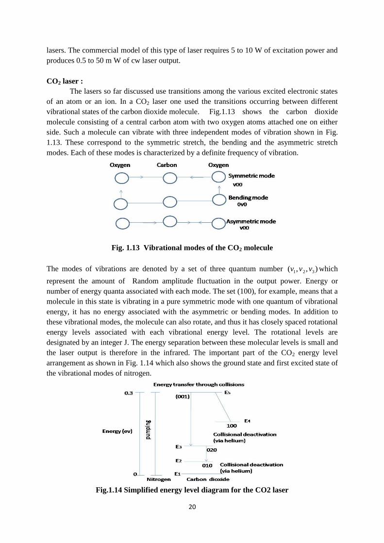
CO2 laser :
The lasers so far discussed use transitions among the various excited electronic states
of an atom or an ion. In a CO2 laser one used the transitions occurring between different
vibrational states of the carbon dioxide molecule. Fig.1.13 shows the carbon dioxide
molecule consisting of a central carbon atom with two oxygen atoms attached one on either
side. Such a molecule can vibrate with three independent modes of vibration shown in Fig.
1.13. These correspond to the symmetric stretch, the bending and the asymmetric stretch
modes. Each of these modes is characterized by a definite frequency of vibration.
Fig. 1.13 Vibrational modes of the CO2 molecule
The modes of vibrations are denoted by a set of three quantum number ),,( 321 vvv which
represent the amount of Random amplitude fluctuation in the output power. Energy or
number of energy quanta associated with each mode. The set (100), for example, means that a
molecule in this state is vibrating in a pure symmetric mode with one quantum of vibrational
energy, it has no energy associated with the asymmetric or bending modes. In addition to
these vibrational modes, the molecule can also rotate, and thus it has closely spaced rotational
energy levels associated with each vibrational energy level. The rotational levels are
designated by an integer J. The energy separation between these molecular levels is small and
the laser output is therefore in the infrared. The important part of the CO2 energy level
arrangement as shown in Fig. 1.14 which also shows the ground state and first excited state of
the vibrational modes of nitrogen.
Fig.1.14 Simplified energy level diagram for the CO2 laser
21
Many CO2 lasers contain a mixture of CO2, nitrogen, helium in the ratio 1:4:5 Nitrogen plays
similar role to that of helium in the He-Ne laser. Excited nitrogen molecules transfer energy
to the CO2 molecules in resonant collisions ; exciting them to the (001) levels. The (100) CO2
levels have a lower energy and cannot be populated in this way, so that population inversion
is created between the (001) and (100) levels giving stimulated emission at about 10.6μm .
The helium has a dual role. Firstly, it increases the thermal conductivity to the walls of the
tube, thereby decreasing the temperature and Doppler broadening, which inturn increases the
gain. Secondly it increases the laser efficiency by indirectly depleting the population of the
(100) level, which is linked by resonant collisions to the (020) and (010) levels, the later
being depleted via collisions with the helium atoms. The CO2 laser possesses an
extremely high efficiency of 30%. This is because of efficient pumping to the (001) level
and also because all the energy levels involved are close to the ground level. Thus the atomic
quantum efficiency which is the ratio of the energy difference corresponding to the laser
transition to the energy difference of the pump transition, ie
15
45
EE
EE
is quite high (45%). Thus a large portion of input power can be converted into useful laser
power. Output powers of several watts to several kilowatts can be obtained from CO2 lasers.
High power CO2 lasers find applications in materials processing, welding, hole drilling,
cutting etc., because of their very high output power. In addition the atmospheric attenuation
is low at 10.6μm which leads to some applications of CO2 lasers in open air communications
(d) Semiconductor lasers
(i) Homojunction laser
Semiconductor lasers are not very different in principle from the light emitting diodes.
A p-n junction provides the active medium. To obtain laser action we have to create
population inversion and provide optical feedback. To obtain stimulated emission, there must
be a region in the device where there are many excited electrons and holes present together.
This is achieved by forming a homojunction from very heavily doped n and p materials. In
such n+ type material, the Fermi level lies within the conduction band. Similarly, for the p+
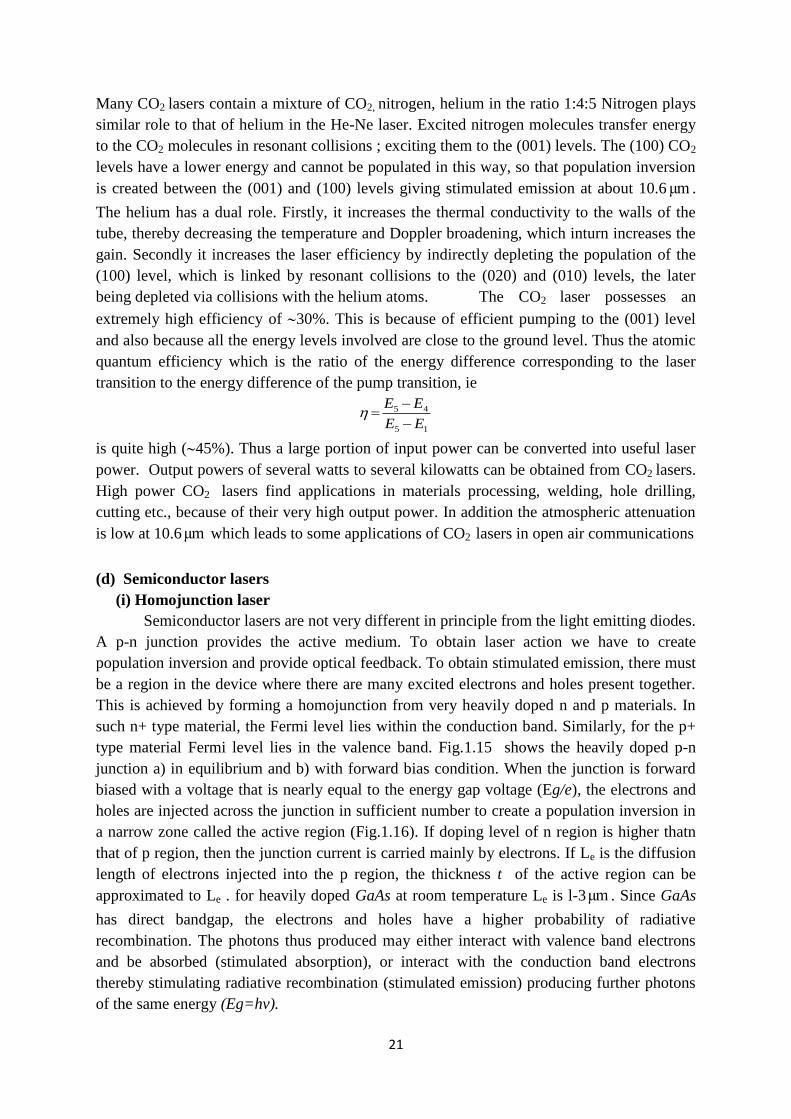
type material Fermi level lies in the valence band. Fig.1.15 shows the heavily doped p-n
junction a) in equilibrium and b) with forward bias condition. When the junction is forward
biased with a voltage that is nearly equal to the energy gap voltage (Eg/e), the electrons and
holes are injected across the junction in sufficient number to create a population inversion in
a narrow zone called the active region (Fig.1.16). If doping level of n region is higher thatn
that of p region, then the junction current is carried mainly by electrons. If Le is the diffusion
length of electrons injected into the p region, the thickness t of the active region can be
approximated to Le . for heavily doped GaAs at room temperature Le is l-3μm . Since GaAs
has direct bandgap, the electrons and holes have a higher probability of radiative
recombination. The photons thus produced may either interact with valence band electrons
and be absorbed (stimulated absorption), or interact with the conduction band electrons
thereby stimulating radiative recombination (stimulated emission) producing further photons
of the same energy (Eg=hv).
22
Fig.1.15 Heavily doped p-n junction (a) in equilibrium and (b) with forward bias.
Fig.1.16 Diagram showing the active region and mode volume of a semiconductor laser
If the injected carrier concentration is large, the stimulated emission can exceed the
absorption so that optical amplification is achieved in the active region. To provide feedback,
there is no need to use external mirrors in the case of diode lasers. The diode is cleaved along
natural crystal plane normal to the plane of the junction so that the end faces are perfectly
parallel. For GaAs, the junction plane is (100) and the cleaved faces are (110) planes. The
high refractive index (3.6) of GaAs ensures sufficiently high reflection at the material / air
interface so that there is no need for separate external mirrors to provide optical feedback.
Laser oscillations occur when the round trip gain exceeds the total losses. In semiconductors,
the major losses are due to scattering at optical inhomogeneties in the semiconductor material
and free carrier absorption.
In the active region additional charge carriers present increases its refractive index
above that of the surrounding material, thereby forming a dielectric waveguide. Since the
difference in refractive index between the centre waveguiding layer and the surrounding
regions is very less (about 0.02 only), the waveguiding effect is not very efficient. Therefore
the radiation generated in the active region extends to some extend beyond the active region,
thereby forming the mode volume. The waveguiding effect achieved in simple homojunction
laser diodes of the form shown in Fig.1.17 just allows the laser action on vigorous pumping.
They can be operated only in the pulsed mode at room temperature because of very high
23
threshold pumping current density (typically of the order of 400 Amm-2
). The onset of laser
action at the threshold current density is indicted by a sudden increase of light output
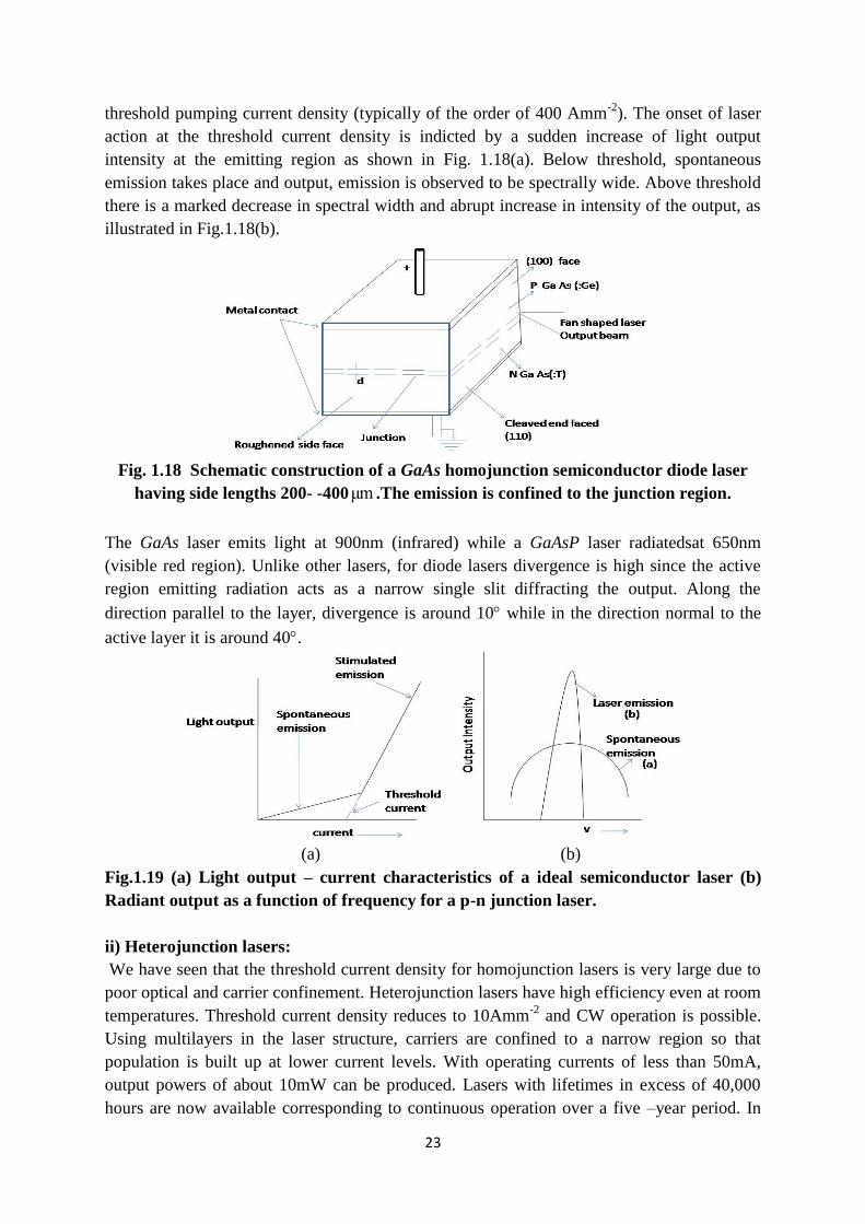
intensity at the emitting region as shown in Fig. 1.18(a). Below threshold, spontaneous
emission takes place and output, emission is observed to be spectrally wide. Above threshold
there is a marked decrease in spectral width and abrupt increase in intensity of the output, as
illustrated in Fig.1.18(b).
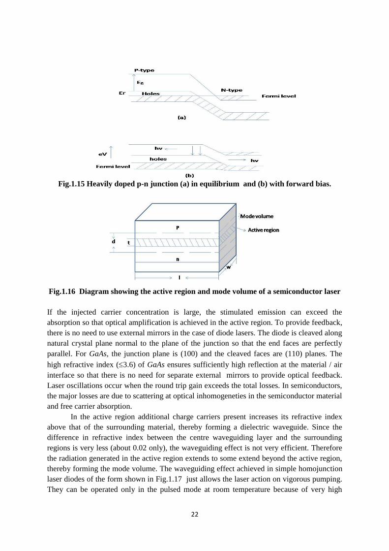
Fig. 1.18 Schematic construction of a GaAs homojunction semiconductor diode laser
having side lengths 200- -400μm .The emission is confined to the junction region.
The GaAs laser emits light at 900nm (infrared) while a GaAsP laser radiatedsat 650nm
(visible red region). Unlike other lasers, for diode lasers divergence is high since the active
region emitting radiation acts as a narrow single slit diffracting the output. Along the
direction parallel to the layer, divergence is around 10 while in the direction normal to the
active layer it is around 40.
(a) (b)
Fig.1.19 (a) Light output – current characteristics of a ideal semiconductor laser (b)
Radiant output as a function of frequency for a p-n junction laser.
ii) Heterojunction lasers:
We have seen that the threshold current density for homojunction lasers is very large due to
poor optical and carrier confinement. Heterojunction lasers have high efficiency even at room
temperatures. Threshold current density reduces to 10Amm-2
and CW operation is possible.
Using multilayers in the laser structure, carriers are confined to a narrow region so that
population is built up at lower current levels. With operating currents of less than 50mA,
output powers of about 10mW can be produced. Lasers with lifetimes in excess of 40,000
hours are now available corresponding to continuous operation over a five –year period. In

24
optical fibre communications, it is desirable to have a laser emitting at wavelengths in the
region 1.1 to 1.6 m , where present optical fibres have minimum attenuation and dispersion.
From lasers fabricated with quaternary compounds such as GaxIn1-xAs1-yPy, wavelengths in
this range can be obtained.
1.13 Applications of Lasers
In 1960, when invented laser was called “an invention in search of applications”.
Nobody was knowing what to do with such an intense, highly directional beam. Very first
application of laser was in the field of medicine but within an year in quite a lot of areas,
lasers started finding their applications. We can now say that there is no field in which lasers
are not being used. Let us see applications of lasers in few fields.
Lasers in Industry : In manufacturing industry lasers are used for welding, cutting and
drilling applications.
Welding : With increased power output, it is possible to use the laser (primarily CO2) as a
welding tool. The advantages of laser welding are:
Very high welding rates are possible (with 10kW CO2 laser 5 mm thick stainless steel
plates can be welded at a speed of 10 cm/sec).
Dissimilar metals can be welded
Minimum amount of distortion of the surrounded are (i.e.very less heat affected zone?
Any extremely complex shaped contours can be welded using computers for
controlling the deflection of the laser beam.
Microwelding is done with great ease.
Being non-contact method, the work piece is not stressed.
Cutting : Lasers cut through a wide variety of materials, rapidly and precisely.
With low – power CO2 laser, insulation from electrical wires and cables are striped
off. While the insulation material absorbs are radiation metal conductor reflects the
same. Hence without any damage to the electrical wire the insulation can be removed.
With high power levels, glass and quart are easily cut with CO2 laser. With 250 watt
CO2 laser 3 mm thick quartz plate can be cut at a rate of 2 cm/sec.
Solid State Physics
With the same laser quoted above, oxygen assisted laser cutting can be done at a rate
of 1cm /sec in a low-carbon steel plate of 1 cm thick.
Any desired shape can be cut.
Cut finish used to be very smooth (cosmetic) requiring no further treatment such as
grinding and polishing.
Lasers are used to cut a large number of models and sizes of dresses and suits.
Synthetic fabrics are particularly suited to this technique, since the cut edges are
melted by the beam and any fraying is prevented.
Drilling : Most drilling systems operate in a pulsed mode. To get the drill of desired depth
and size, number of pulses, and the energy of each pulse are to be controlled.
One of the first application of the laser was to drill diamond dies used in the extrusion
of wire.
25
Lasers are used to drill aerosol nozzles and control orifices within the required
precision.
Lasers are used to drill holes in ‘difficult to drill’ materials such as ceramics etc.
Holes of micron order can be easily drilled using lasers. (In this small range drill bits
can not be used).
Head treatment :Head treatment is common in the tooling and automotive industry.
Wherever it is desirable to treat only a portion of a large item, lasers are very useful.
For example, an automobile piston ring alone has to be heat treated and hardened
without affecting the entire piston.
The greatest advantage of use of laser system in industry is that a single system can be
used for all the above applications by proper adjustment of its power. Being non contact
method the entire region is stress free.
Lasers in electronic industry: Lasers are widely used for material processing in electronic
industry. Let us see few such important applications.
Scribing
Scribing involves drawing fine lines in brittle ceramic and semiconductor wafers.
When bent they break along the line scribed. Low power CO2 lasers are generally used for
this purpose.
Soldering
‘Difficult to solder’ material such as platinum, silver, palladium are soldered using
lasers. Sheets as thin as 25 micron can be soldered without any damage to the sheet. This is a
fluxless soldering and non – contact method. Nd: YAG laser is used for this process.
Trimming
Film resistor trimming is effectively carried out using Nd: YAG laser. First a film of
higher thickness and hence lower resistance value is taken. Using pulsed laser without
thermal damage to the substrate, the resistance material is gradually removed from the
surface and its resistance is continuously monitored and controlled.
Lasers in Medicine
The very first application of laser was in the field of medicine :
Ophthalmologists started using Argon ion lasers for welding retinal detachment. The
retina is the light sensitive layer at the back of the eye. If it is torn and extends it may
lead to blindness. The green beam of Argon ion laser is strongly absorbed by red blood
cells of the retina and welds the retina back to the eye ball. Since this beam passes
through the eye lens and the vitrious chamber without being absorbed, this treatment is
done without surgery.
For cataract removal lasers are used
Using ultraviolet radiation from Excimer laser, eye lens curvature correction is being
carried out. This is based on photoablative effect invented by Prof.Srinivasan.
Laser scalpels are used for bloodless surgery. When the tissues are cut the blood veins
cut are fused at their tips by the infrared laser and hence there is no blood loss.
In laser angioplasty for removal of artery block Nd: YAG lasers are used. The laser
radiation is sent through fiber to the region of block, burns the excess growth and
regulates the blood flow without need for bypass surgery.
26
In dermatology, lasers are used to remove freckles, acne, birth marks and tattoo. When
such regions are illuminated with blue-green laser light, the radiation is absorbed by
the blood and heats up. The blood vessels are closed and excess blood flow is stopped.
Lasers are used in destroying kidney stones and gallstones. Laser pulses sent through
optical fibers shatter the stones into small pieces.
Lasers are used in cancer diagnosis and therapy. When suscept growth region is
illuminated with ultraviolet laser, the porferin, a natural dye accumulated in cancerous
region glows with red colour indicating the presence of cancerous cells. When
photosensitive dye is injected into the patient’s body, the dye is concentrated in cancer
cells. When suscept areas are illuminated with laser of approximate wavelength, cancer
cells are destroyed.
Lasers in Scientific Fields
It is impossible to list out all the applications of lasers in scientific fields. Let us see
few important applications.
Lasers in metrology
When Amstrong landed in the moon in 1969, he placed a reflecting mirror there. A
pulsed laser pulse was sent from the earth to the moon; its reflected signal was received and
the distance between the earth and the moon was calculated with centimetre accuracy. Now-
a-days for surveying and aligement lasers are used. Using laser interferometry any
displacement can be measured with an accuracy of nanometer (10-9
m).
Lasers in defence
Lasers are finding wide range of applications such as ranging, guiding weapons to the
intended target and beam itself acting as a weapon.
Pulsed laser beam directed towards the target returns after reflection. The time-delay
in its round-trip is measured to determine the range of the target. If the object is in
motion, the reflected signal is Doppler shifted and by measuring this shift the velocity
of the moving object is also calculated. Nd: YAG or Nd: glass lasers are used for this
purpose.
Lasers are used to guide the missiles. The head of the missile sends a laser beam to
the target and from the collection of light scattered from the target, the angle of line of
sight is determined. The difference, if any, between the glide angle of the trajectory of
bomb and the angle of line of sight is fed to servo loop acting as the error signal. The
error correcting signal controls the direction of motion of the bomb and brings it onto
the target. Since infrared radiation is not absorbed by fog, smoke or haze in the
atmosphere, CO2 lasers are used for this purpose.
Laser weapons have two uses in defence ; one to disable the enemy weapons and
another to destroy them. Lasers with moderate powers are used to damage the infrared
sensors on guided missies or the sensitive electronic eyes of spy satellites. To destroy
the weapons very high powers (of megawatts order) are required. Still there are many
problems associated with such programmes.
Lasers in nuclear energy
Nuclear fusion offers a low cost and pollution free energy. Extremely high
temperature and pressures are required in order to make light nuclei to overcome
27
their mutual repulsion and combine to release energy. Laser assisted inertial
confinement method generates highly compressed plasma of heavy isotopes of
hydrogen, namely deuterium D and tritium T. In the presence of such high
compression, the core reaches a temperature of about 108K. To achieve these
conditions enormous amount of laser pulse energy is needed. Many countries are in
the process of development of laser fusion projects.
Lasers are used for isotope separation. Isotopes are chemically almost identical.
Each isotope absorbs light at different characteristic wavelength. Using a tunable
dye laser it is possible to ionize one isotope without disturbing the other. Ionized
isotope can be separated from the other using electrostatic fields. From natural U-
238, ionized U=235 atoms are separated using this method.
Lasers in optical communications
The amount of information that can be sent over an electro magnetic wave is
proportional to the bandwidth of the wave. Since lasers operate with exceedingly large
bandwidth, optical communication using lasers is very attractive.
Lasers are used in two types of communication, one, open space communication and
another fibre optic communication.
Open space communication requires the environment free from fog, dust and rain.
Since lasers are highly directional laser communication is very attractive when
compared to microwave communication (To achieve the directionality as that of the
laser of beam waist I mm diameter, the microwave antenna must be 100m in
diameter)
Now-a-days conventional metallic cables are replaced by fiber optic cables because of
the following advantages.
1. Enormous bandwidth (as large as 105 GHz)
2. Electrical isolation
3. Immunity to interference and cross talk
4. Signal security
5. Small size and weight
6. Low transmission loss
7. Ruggedness and flexibility
8. Low cost
Lasers in consumer electronics industry
Diode lasers as well as low power He-Ne lasers are used in different consumer
electronic industries. They are used every day in different fields.
Supermarket scanners.
Now-a-days on almost all consumer items, bar codes are printed. When laser light
scans the bar code label, the dark lines of the code absorb light while the bright lines reflect
light. This light modulation is registered by a photosensitive light detector. This information
passes to the computer which in turn identifies the product and displays the price. Such bar
codes are used in libraries also.
28
Unit - II
Basics of Semiconductors
2.1. Nature of Light:
The scientific study of the behavior of light is called optics and covers reflection of
light by a mirror or other object, refraction by a lens or prism, diffraction of light as it passes
by the edge of an opaque object, and interference patterns resulting from diffraction. Also
studied is the polarization of light. Any successful theory of the nature of light must be able
to explain these and other optical phenomena.
(a) The Wave, Particle, and Electromagnetic Theories of Light:
The earliest scientific theories of the nature of light were proposed around the end of the
17th century. In 1690, Christian Huygens proposed a theory that explained light as a wave
phenomenon. However, a rival theory was offered by Sir Isaac Newton in 1704. Newton,
who had discovered the visible spectrum in 1666, held that light is composed of tiny
particles, or corpuscles, emitted by luminous bodies. By combining this corpuscular theory
with his laws of mechanics, he was able to explain many optical phenomena.
For more than 100 years, Newton's corpuscular theory of light was favored over the wave
theory, partly because of Newton's great prestige and partly because not enough experimental
evidence existed to provide an adequate basis of comparison between the two theories.
Finally, important experiments were done on the diffraction and interference of light by
Thomas Young (1801) and A. J. Fresnel (1814–15) that could only be interpreted in terms of
the wave theory. The polarization of light was still another phenomenon that could only be
explained by the wave theory. Thus, in the 19th century, the wave theory became the
dominant theory of the nature of light. The wave theory received additional support from the
electromagnetic theory of James Clerk Maxwell (1864), who showed that electric and
magnetic fields were propagated together and that their speed was identical with the speed of
light. It thus became clear that visible light is a form of electromagnetic radiation,
constituting only a small part of the electromagnetic spectrum. Maxwell's theory was
confirmed experimentally with the discovery of radio waves by Heinrich Hertz in 1886.
(b) Modern Theory of the Nature of Light:
With the acceptance of the electromagnetic theory of light, only two general problems
remained. One of these was that of the luminiferous ether, a hypothetical medium suggested
as the carrier of light waves, just as air or water carries sound waves. The ether was assumed
to have some very unusual properties, e.g., being massless but having high elasticity. A
number of experiments performed to give evidence of the ether, most notably by A. A.
Michelson in 1881 and by Michelson and E. W. Morley in 1887, failed to support the ether
hypothesis. With the publication of the special theory of relativity in 1905 by Albert Einstein,
the ether was shown to be unnecessary to the electromagnetic theory.
29
The second main problem, and the more serious of the two, was the explanation of various
phenomena, such as the photoelectric effect, that involved the interaction of light with matter.
Again the solution to the problem was proposed by Einstein, also in 1905. Einstein extended
the quantum theory of thermal radiation proposed by Max Planck in 1900 to cover not only
vibrations of the source of radiation but also vibrations of the radiation itself. He thus
suggested that light, and other forms of electromagnetic radiation as well, travel as tiny
bundles of energy called light quanta, or photons. The energy of each photon is directly
proportional to its frequency.
With the development of the quantum theory of atomic and molecular structure by Niels
Bohr and others, it became apparent that light and other forms of electromagnetic radiation
are emitted and absorbed in connection with energy transitions of the particles of the
substance radiating or absorbing the light. In these processes, the quantum, or particle, nature
of light is more important than its wave nature. When the transmission of light is under
consideration, however, the wave nature dominates over the particle nature. In 1924, Louis de
Broglie showed that an analogous picture holds for particle behavior, with moving particles
having certain wavelike properties that govern their motion, so that there exists a
complementarity between particles and waves known as particle-wave duality. The quantum
theory of light has successfully explained all aspects of the behavior of light.
2.2. Light sources:
There are many sources of light. The most common light sources are thermal: a body at a
given temperature emits a characteristic spectrum of black-body radiation. A simple thermal
source is sunlight, the radiation emitted by the chromosphere of the Sun at around 6,000
kelvins (5,730 degrees Celsius; 10,340 degrees Fahrenheit) and roughly 44% of sunlight
energy that reaches the ground is visible.
Another example is incandescent light bulbs, which emit only around 10% of their energy
as visible light and the remainder as infrared. A common thermal light source in history is the
glowing solid particles in flames, but these also emit most of their radiation in the infrared,
and only a fraction in the visible spectrum.
Atoms emit and absorb light at characteristic energies. This produces "emission lines" in the
spectrum of each atom. Emission can be spontaneous, as in light-emitting diodes, gas
discharge lamps (such as neon lamps and neon signs, mercury-vapor lamps, etc.), and flames
(light from the hot gas itself—so, for example, sodium in a gas flame emits characteristic
yellow light). Emission can also be stimulated, as in a laser or a microwave maser.
Deceleration of a free charged particle, such as an electron, can produce visible radiation:
cyclotron radiation, synchrotron radiation, and bremsstrahlung radiation are all examples of
this. Particles moving through a medium faster than the speed of light in that medium can
produce visible Cherenkov radiation.
Certain chemicals produce visible radiation by chemoluminescence. In living things, this
process is called bioluminescence. For example, fireflies produce light by this means, and
boats moving through water can disturb plankton which produce a glowing wake. Certain
substances produce light when they are illuminated by more energetic radiation, a process
30
known as fluorescence. Some substances emit light slowly after excitation by more energetic
radiation. This is known as phosphorescence. Phosphorescent materials can also be excited
by bombarding them with subatomic particles. Cathodoluminescence is one example. This
mechanism is used in cathode ray tube television sets and computer monitors.
The two important semiconductor light sources widely used are LED’s and LASER diodes.
The dominant operating process for the LED is spontaneous emission and for the LASER, it
is stimulated emission.
Certain other mechanisms can produce light:
(i) Bioluminescence (ii) Cherenkov radiation (iii) Electroluminescence (iv)
Scintillation (v) Sonoluminescence (vi) Triboluminescence.
When the concept of light is intended to include very-high-energy photons (gamma rays),
additional generation mechanisms include: (i) Particle–antiparticle annihilation (ii)
Radioactive decay
General characteristics of light sources: Some of the important characteristics of light
sources have been discussed in the following.
(i) Drive current vs light output: When injected carriers cross the junction, they can
recombine by a radiative process which produces light or by a nonradiative process which
produces heat. The ratio between these two processes is dependent on the current density
(Amp/cm2) of semiconductor junction area. At low forward voltages, the diode current is
dominated by the nonradiative recombination current, mainly due to surface recombination’s
near the perimeter of the LED chip. At higher forward voltages, the diode current is
dominated by the radiative diffusion current. At even higher voltages, the diode current will
be limited by the series resistance. Also, at high forward drive currents the junction
temperature of the semiconductor increases due to significant power dissipation. This
increase in temperature results in a decrease in the radiative recombination efficiency. As the
current density is further increased, internal series resistance effects will also tend to reduce
the light generating efficiency of the light source.
(ii) Quantum efficiency: Quantum efficiency (η) is defined as the ratio of the radiative
recombination rate (Rr) to total recombination rate (Rt) and is given by
η=Rr/Rt ⋅⋅⋅ (2.2)
(iii) Switching speed: The term switching speed refers to how fast a light source can be
turned on and off by an electrical signal to produce a corresponding optical output pattern.
Laser diodes offer faster switching speeds than LED’s.
(iv) Peak spectral wavelength: The wavelength at which the maximum amount of light is
generated is called the peak wavelength (λP). It is determined by the energy band gap of the
semiconductor material used.
31
(v) Spectral width: The range of wavelengths over which a light source emits light. The
light source needs to emit light within a narrow spectral width. The spectral width of the
LASER diode is very narrow compared to LED.
2.3. Black body:
A black body is an idealized physical body that absorbs all incident electromagnetic
radiation, regardless of frequency or angle of incidence. A white body is one with a "rough
surface [that] reflects all incident rays completely and uniformly in all directions. A black
body in thermal equilibrium (that is, at a constant temperature) emits electromagnetic
radiation called black-body radiation. The radiation is emitted according to Planck's law,
meaning that it has a spectrum that is determined by the temperature alone, not by the body's
shape or composition. A black body in thermal equilibrium has two notable properties:
(i) It is an ideal emitter: at every frequency, it emits as much energy as – or more energy
than – any other body at the same temperature. (ii) It is a diffuse emitter: the energy is
radiated isotropically, independent of direction.
An approximate realization of a black surface is a hole in the wall of a large enclosure. Any
light entering the hole is reflected indefinitely or absorbed inside and is unlikely to re-
emerge, making the hole a nearly perfect absorber. The radiation confined in such an
enclosure may or may not be in thermal equilibrium, depending upon the nature of the walls
and the other contents of the enclosure. Real materials emit energy at a fraction—called the
emissivity—of black-body energy levels. By definition, a black body in thermal equilibrium
has an emissivity of ε = 1.0. A source with lower emissivity independent of frequency often
is referred to as a gray body. Construction of black bodies with emissivity as close to one as
possible remains a topic of current interest. In astronomy, the radiation from stars and planets
is sometimes characterized in terms of an effective temperature, the temperature of a black
body that would emit the same total flux of electromagnetic energy.
2.4. Colour temperature:
The colour temperature of a light source is the temperature of an ideal black-body radiator
that radiates light of comparable hue to that of the light source. Colour temperature is a
characteristic of visible light that has important applications in lighting, photography,
videography, publishing, manufacturing, astrophysics, horticulture, and other fields. In
practice, colour temperature is only meaningful for light sources that do in fact correspond
somewhat closely to the radiation of some black body, i.e., those on a line from
reddish/orange via yellow and more or less white to blueish white; it does not make sense to
speak of the color temperature of, e.g., a green or a purple light. Colour temperature is
conventionally expressed in Kelvin, using the symbol K, a unit of measure for temperature
based on the Kelvin scale.
Colour temperatures over 5,000K are called cool colours (bluish white), while lower color
temperatures (2,700–3,000 K) are called warm colours (yellowish white through red). This
32
relation, however, is a psychological one in contrast to the physical relation implied by
Wien's displacement law, according to which the spectral peak is shifted towards shorter
wavelengths (resulting in a more blueish white) for higher temperatures.
Categorizing different lighting: The colour temperature of the electromagnetic radiation
emitted from an ideal black body is defined as its surface temperature in Kelvin, or
alternatively in mireds (micro-reciprocal Kelvin). This permits the definition of a standard by
which light sources are compared.
To the extent that a hot surface emits thermal radiation but is not an ideal black-body
radiator, the colour temperature of the light is not the actual temperature of the surface. An
incandescent lamp's light is thermal radiation, and the bulb approximates an ideal black-body
radiator, so its colour temperature is essentially the temperature of the filament. Thus a
relatively low temperature emits a dull red and a high temperature emits the almost white of
the traditional incandescent light bulb.
Many other light sources, such as fluorescent lamps, or LEDs (light emitting diodes) emit
light primarily by processes other than thermal radiation. This means that the emitted
radiation does not follow the form of a black-body spectrum. These sources are assigned
what is known as a correlated color temperature (CCT). CCT is the color temperature of a
black-body radiator which to human colour perception most closely matches the light from
the lamp. Because such an approximation is not required for incandescent light, the CCT for
an incandescent light is simply its unadjusted temperature, derived from the comparison to a
black-body radiator.
The Sun closely approximates a black-body radiator. The effective temperature, defined by
the total radiative power per square unit, is about 5,780 K. The colour temperature of sunlight
above the atmosphere is about 5,900 K. As the Sun crosses the sky, it may appear to be red,
orange, yellow or white depending on its position. The changing colour of the Sun over the
course of the day is mainly a result of scattering of light and is not due to changes in black-
body radiation. The blue colour of the sky is caused by Rayleigh scattering of the sunlight
from the atmosphere, which tends to scatter blue light more than red light. Some early
morning and evening light (golden hours) has a lower color temperature due to increased
low-wavelength light scattering by the Tyndall effect. This effect was especially pronounced
with the increase in small dust particles in the atmosphere after the eruptions of Mount
Tambora in 1815 and Krakatoa in 1883, which gave rise to intense red sunsets around the
world. Daylight has a spectrum similar to that of a black body with a correlated color
temperature of 6,500 K or 5,500 K (daylight-balanced photographic film standard)
Applications: Some of the applications of colour temperature is given below.
(i) Lighting - For lighting building interiors, it is often important to take into account the
colour temperature of illumination. For example, a warmer (i.e., lower colour temperature)
light is often used in public areas to promote relaxation, while a cooler (higher color
temperature) light is used to enhance concentration in offices.
33
(ii) Aquaculture - In fishkeeping, colour temperature has different functions and foci, for
different branches. In freshwater aquaria, colour temperature is generally of concern only for
producing a more attractive display. Lights tend to be designed to produce an attractive
spectrum, sometimes with secondary attention to keeping plants alive. In a saltwater/reef
aquarium, colour temperature is an essential part of tank health. Within about 400 to 3000
nanometers, light of shorter wavelength can penetrate deeper into water than longer
wavelengths, providing essential energy sources to the algae hosted in (and sustaining) coral.
(iii) Digital photography - In digital photography, colour temperature is sometimes used
interchangeably with white balance, which allow a remapping of colour values to simulate
variations in ambient colour temperature.
(iv) Photographic film: Photographic film is made for specific light sources (most
commonly daylight film and tungsten film), and used properly, will create a neutral colour
print. Matching the sensitivity of the film to the colour temperature of the light source is one
way to balance colour. If tungsten film is used indoors with incandescent lamps, the
yellowish-orange light of the tungsten incandescent lamps will appear as white (3,200 K) in
the photograph. Colour negative film is almost always daylight-balanced, since it is assumed
that colour can be adjusted in printing (with limitations; see above). Colour transparency
film, being the final artefact in the process, has to be matched to the light source or filters
must be used to correct colour. Filters on a camera lens, or colour gels over the light source(s)
may be used to correct colour balance.
(v) Desktop publishing: In the desktop publishing industry, it is important to know a
monitor’s colour temperature. Colour matching software, such as Apple's ColorSync for Mac
OS, will measure a monitor's color temperature and then adjust its settings accordingly.
Common monitor color temperatures, along with matching standard illuminants in
parentheses, are as follows:
5,000 K (D50), 5,500 K (D55), 6,500 K (D65), 7,500 K (D75), 9,300 K.
Digital cameras, web graphics, DVDs, etc., are normally designed for a 6,500 K colour
temperature. The sRGB standard commonly used for images on the Internet stipulates
(among other things) a 6,500 K display whitepoint.
(vi) TV, video, and digital still cameras : Most video and digital still cameras can adjust
for colour temperature by zooming into a white or neutral coloured object and setting the
manual "white balance" the camera then shows true white as white and adjusts all the other
colours accordingly. White-balancing is necessary especially when indoors under fluorescent
lighting and when moving the camera from one lighting situation to another. Most cameras
also have an automatic white balance function that attempts to determine the colour of the
light and correct accordingly. While these settings were once unreliable, they are much
improved in today's digital cameras, and will produce an accurate white balance in a wide
variety of lighting situations.

34
2.5. Units of Light:
Table 2.1 SI Radiometry units
Quantity Unit Name Symbol Name Symbol Radiant energy Qe joule J
Radiant energy density
we joule per cubic metre J/m3
Radiant flux Φe watt W Spectral flux
Φe,ν (or)
Φe,λ watt per hertz (or) watt per metre W/Hz (or) W/m
Radiant intensity Ie,Ω
watt per steradian W
Spectral intensity Ie,Ω,ν
watt per steradian per hertz W⋅sr−1⋅Hz−1
Radiance
Le,Ω watt per steradian per square metre W⋅sr−1⋅m−2
Spectral radiance
Le,Ω,ν watt per steradian per square metre per
hertz W⋅sr
−1⋅m−2⋅Hz−1
Irradiance Ee watt per square metre W/m2
Radiosity Je watt per square metre W/m2
Spectral radiosity Je,ν
watt per square metre per hertz W⋅m−2⋅Hz−1
Radiant exitance Me watt per square metre W/m2 M⋅T−3
Spectral exitance
Me,ν watt per square metre per hertz W⋅m−2⋅Hz−1
Radiant exposure He joule per square metre J/m2
Spectral exposure He,ν joule per square metre per hertz J⋅m−2⋅Hz−1
Hemispherical emissivity ε
Spectral hemispherical εν
Directional emissivity ε Ω
Spectral directional
emissivity
εΩ,ν
Hemispherical
absorptance
A
Spectral hemispherical
absorptance
Aν
Directional absorptance AΩ
Spectral directional
absorptance
AΩ,ν
Hemispherical
reflectance
R
Spectral hemispherical
reflectance
Rν
Directional reflectance RΩ
Spectral directional
reflectance
RΩ,ν
Hemispherical
transmittance
T
Spectral hemispherical
transmittance
Tν
Directional transmittance TΩ
Spectral directional
transmittance
TΩ,ν
35
Table 2.2. SI photometric units:
2.6. Semiconductor Basics:
(i) Intrinsic semiconductors: Semiconductors materials such as silicon (Si), germanium
(Ge) and gallium arsenide (GaAs), have electrical properties somewhere in the middle,
between those of a “conductor” and an “insulator”. They are not good conductors nor good
insulators (hence their name “semi”-conductors). They have very few “free electrons” and are
able to flow, but only under special conditions. The ability of semiconductors to conduct
electricity can be greatly improved by replacing or adding certain donor or acceptor atoms to
this crystalline structure thereby, producing more free electrons than holes or vice versa. That
is by adding a small percentage of another element to the base material, either silicon or
germanium. On their own Silicon and Germanium are classed as intrinsic semiconductors,
that is they are chemically pure, containing nothing but semi-conductive material. But by
controlling the amount of impurities added to this intrinsic semiconductor material it is
possible to control its conductivity. Various impurities called donors or acceptors can be
added to this intrinsic material to produce free electrons or holes respectively. This process
Hemispherical
attenuation coefficient
μ reciprocal metre m−1
Spectral hemispherical
coefficient attenuation
μν reciprocal metre m−1
Directional attenuation
coefficient
μΩ reciprocal metre m−1
Spectral directional
attenuation
coefficient.
μΩ,ν reciprocal metre m−1
Quantity Unit
Name Symbol Name Symbol
Luminous energy Qv lumen second lm⋅s
Luminous flux / luminous
power
Φv lumen (= cd⋅sr) lm
Luminous intensity Iv candela (= lm/sr) cd
Luminance
Lv candela per square metre cd/m2
Illuminance Ev lux (= lm/m2) lx
Luminous exitance /
luminous emittance Mv lux lx
Luminous exposure Hv lux second lx⋅s
Luminous energy density
ωv lumen second per cubic metre lm⋅s⋅m−3
Luminous efficacy η lumen per watt lm/W
Luminous efficiency /
luminous coefficient V
36
of adding donor or acceptor atoms to semiconductor atoms (the order of 1 impurity atom per
10 million (or more) atoms of the semiconductor) is called Doping.
A Silicon Atom Structure: The diagram shows the structure and lattice of a ‘normal’ pure
crystal of Silicon (Fig.2.1)
Fig.2.1 A Silicon Atom Structure
The as the doped silicon is no longer pure, these donor and acceptor atoms are collectively
referred to as “impurities”, and by doping these silicon material with a sufficient number of
impurities, we can turn it into a semi-conductor. The most commonly used semiconductor
basics material by far is Silicon. Silicon has four valence electrons in its outermost shell
which it shares with its neighbouring silicon atoms to form full orbital’s of eight electrons.
The structure of the bond between the two silicon atoms is such that each atom shares one
electron with its neighbour making the bond very stable. As there are very few free electrons
available to move around the silicon crystal, crystals of pure silicon (or germanium) are
therefore good insulators, or at the very least very high value resistors. Silicon atoms are
arranged in a definite symmetrical pattern making them a crystalline solid structure. A crystal
of pure silica (silicon dioxide or glass) is generally said to be an intrinsic crystal (it has no
impurities) and therefore has no free electrons. But simply connecting a silicon crystal to a
battery supply is not enough to extract an electric current from it. To do that we need to
create a “positive” and a “negative” pole within the silicon allowing electrons and therefore
electric current to flow out of the silicon. These poles are created by doping the silicon with
certain impurities.
(ii) Extrinsic semiconductors
(a) N-type Semiconductor Basics: In order for our silicon crystal to conduct
electricity, we need to introduce an impurity atom such as Arsenic, Antimony or Phosphorus
into the crystalline structure making it extrinsic (impurities are added). These atoms have five
outer electrons in their outermost orbital to share with neighbouring atoms and are commonly
called “Pentavalent” impurities. This allows four out of the five orbital electrons to bond with
its neighbouring silicon atoms leaving one “free electron” to become mobile when an
electrical voltage is applied (electron flow). As each impurity atom “donates” one electron,
pentavalent atoms are generally known as “donors”. Antimony (symbol Sb) or Phosphorus
(symbol P), are frequently used as a pentavalent additive to the silicon as they have 51
electrons arranged in five shells around their nucleus with the outermost orbital having five
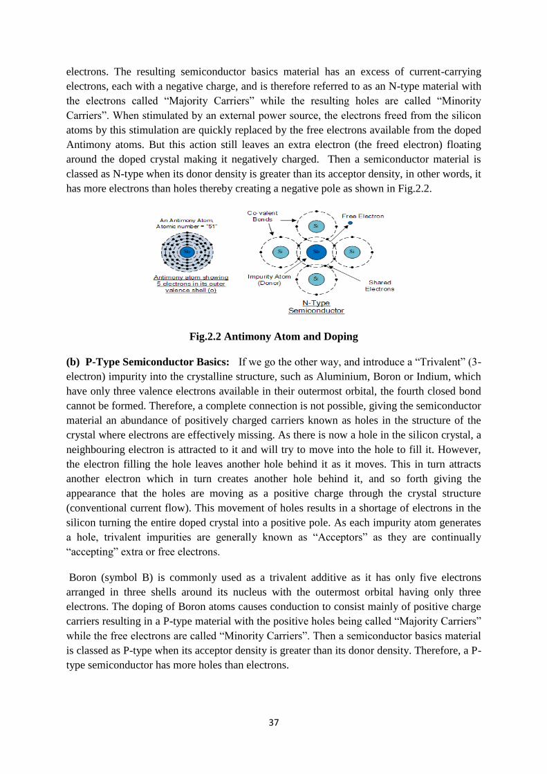
37
electrons. The resulting semiconductor basics material has an excess of current-carrying
electrons, each with a negative charge, and is therefore referred to as an N-type material with
the electrons called “Majority Carriers” while the resulting holes are called “Minority
Carriers”. When stimulated by an external power source, the electrons freed from the silicon
atoms by this stimulation are quickly replaced by the free electrons available from the doped
Antimony atoms. But this action still leaves an extra electron (the freed electron) floating
around the doped crystal making it negatively charged. Then a semiconductor material is
classed as N-type when its donor density is greater than its acceptor density, in other words, it
has more electrons than holes thereby creating a negative pole as shown in Fig.2.2.
Fig.2.2 Antimony Atom and Doping
(b) P-Type Semiconductor Basics: If we go the other way, and introduce a “Trivalent” (3-
electron) impurity into the crystalline structure, such as Aluminium, Boron or Indium, which
have only three valence electrons available in their outermost orbital, the fourth closed bond
cannot be formed. Therefore, a complete connection is not possible, giving the semiconductor
material an abundance of positively charged carriers known as holes in the structure of the
crystal where electrons are effectively missing. As there is now a hole in the silicon crystal, a
neighbouring electron is attracted to it and will try to move into the hole to fill it. However,
the electron filling the hole leaves another hole behind it as it moves. This in turn attracts
another electron which in turn creates another hole behind it, and so forth giving the
appearance that the holes are moving as a positive charge through the crystal structure
(conventional current flow). This movement of holes results in a shortage of electrons in the
silicon turning the entire doped crystal into a positive pole. As each impurity atom generates
a hole, trivalent impurities are generally known as “Acceptors” as they are continually
“accepting” extra or free electrons.
Boron (symbol B) is commonly used as a trivalent additive as it has only five electrons
arranged in three shells around its nucleus with the outermost orbital having only three
electrons. The doping of Boron atoms causes conduction to consist mainly of positive charge
carriers resulting in a P-type material with the positive holes being called “Majority Carriers”
while the free electrons are called “Minority Carriers”. Then a semiconductor basics material
is classed as P-type when its acceptor density is greater than its donor density. Therefore, a P-
type semiconductor has more holes than electrons.
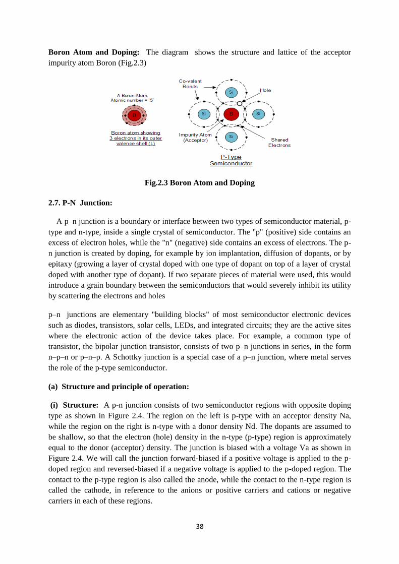
38
Boron Atom and Doping: The diagram shows the structure and lattice of the acceptor
impurity atom Boron (Fig.2.3)
Fig.2.3 Boron Atom and Doping
2.7. P-N Junction:
A p–n junction is a boundary or interface between two types of semiconductor material, p-
type and n-type, inside a single crystal of semiconductor. The "p" (positive) side contains an
excess of electron holes, while the "n" (negative) side contains an excess of electrons. The p-
n junction is created by doping, for example by ion implantation, diffusion of dopants, or by
epitaxy (growing a layer of crystal doped with one type of dopant on top of a layer of crystal
doped with another type of dopant). If two separate pieces of material were used, this would
introduce a grain boundary between the semiconductors that would severely inhibit its utility
by scattering the electrons and holes
p–n junctions are elementary "building blocks" of most semiconductor electronic devices
such as diodes, transistors, solar cells, LEDs, and integrated circuits; they are the active sites
where the electronic action of the device takes place. For example, a common type of
transistor, the bipolar junction transistor, consists of two p–n junctions in series, in the form
n–p–n or p–n–p. A Schottky junction is a special case of a p–n junction, where metal serves
the role of the p-type semiconductor.
(a) Structure and principle of operation:
(i) Structure: A p-n junction consists of two semiconductor regions with opposite doping
type as shown in Figure 2.4. The region on the left is p-type with an acceptor density Na,
while the region on the right is n-type with a donor density Nd. The dopants are assumed to
be shallow, so that the electron (hole) density in the n-type (p-type) region is approximately
equal to the donor (acceptor) density. The junction is biased with a voltage Va as shown in
Figure 2.4. We will call the junction forward-biased if a positive voltage is applied to the p-
doped region and reversed-biased if a negative voltage is applied to the p-doped region. The
contact to the p-type region is also called the anode, while the contact to the n-type region is
called the cathode, in reference to the anions or positive carriers and cations or negative
carriers in each of these regions.
39
Figure 2.4: Cross-section of a p-n junction
(ii) Formation of the Depletion Region: At the instant of the PN junction formation free
electrons near the junction diffuse across the junction into the P region and combine with
holes. Filling a hole makes a negative ion and leaves behind a positive ion on the N side.
These two layers of positive and negative charges form the depletion region, as the region
near the junction is depleted of charge carriers (Fig.2.5). As electrons diffuse across the
junction a point is reached where the negative charge repels any further diffusion of
electrons. The depletion region now acts as a barrier.
(iii) Barrier Potential: The electric field formed in the depletion region acts as a barrier.
External energy must be applied to get the electrons to move across the barrier of the electric
field. The potential difference required to move the electrons through the electric field is
called the barrier potential. Barrier potential of a PN junction depends on the type of
semiconductor material, amount of doping and temperature. This is approximately 0.7V for
silicon and 0.3V for germanium
Fig.2.5 Formation of the depletion region
(iv) Energy Diagrams of PN Junction: The valence band and conduction band in N-Type
material are slightly lower than that of P-Type material As diffusion occurs the depletion
region forms and the energy level of the N region conduction band drops, causing alignment
of the top of the N region conduction band and the bottom of the P region conduction band.
At this point the energy bands are at equilibrium. There is an energy gradient across the
depletion region that a N region electron must climb to get to the P region (Fig.2.6).
40
Fig.2.6 Energy Diagrams of PN Junction
(b) Biasing the PN Junction.
(i) Forward Bias: An external D.C. voltage is applied to a PN junction to bias it
(Fig.2.7(a)). Forward bias allows current through a PN junction. Bias voltage imparts
sufficient energy to the free electrons so they overcome the barrier potential and move into
the P region. Conduction occurs with electron current in the N-Type material and hole current
in the P-Type material. As more electrons and holes flow in the depletion region the number
of positive and negative ions is reduced, causing the depletion region to narrow. The energy
loss in overcoming the barrier potential results in a voltage drop across the PN junction equal
to the barrier potential. ( 0.7V for Si, 0.3V for Ge.) . When a PN junction is forward biased
the N region conduction band is raised to a higher level that overlaps with the P region
conduction band (Fig.2.7(b)).
(a) (b)
Fig.2.7 Biasing the PN Junction. (a) Forward bias (b) Energy band diagram
(ii) Reverse Bias : Reverse bias prevents current flow through a PN junction (Fig2.8(a)).
Reverse bias potential attracts the majority carriers away from the PN junction widening the
depletion region. The potential across the depletion region is equal to the bias voltage.
Reverse current can flow through the PN junction due to minority carriers. When a PN
junction is reverse biased the energy hill increases (Fig.2.8(b)).
(iii) Reverse Breakdown: If the reverse bias voltage is increased to the breakdown voltage,
the reverse current will drastically increase. This is due to collisions of fast minority carriers
41
with atoms, knocking out valence electrons. This process avalanches and results in a high
reverse current damaging the PN structure.
(a) (b)
Fig.2.8 Biasing the PN Junction. (a) Reverse bias (b) Energy band diagram
(c) Generation and recombination processes:
Carrier generation and recombination occur when an electron makes transition from the
valence band to conduction band in a semiconductor, as a result of interaction with other
electrons, holes, photons, or the vibrating crystal lattice itself. These processes must conserve
both quantized energy and momentum, and the vibrating lattice plays a large role in
conserving momentum as photons carry very little momentum in relation to their energy.
Recombination and generation are always happening in semiconductors, both optically and
thermally, and their rates are in balance at equilibrium. The product of the electron and hole
densities (n and p) is a constant (n0 p0 = ni2
) at equilibrium, maintained by recombination
and generation occurring at equal rates. When there is a surplus of carriers (i.e., n p > ni2 ),
the rate of recombination becomes greater than the rate of generation, driving the system
back towards equilibrium . Likewise, when there is a deficit of carriers (i.e., n p < n i 2), the
generation rate becomes greater than the recombination rate, again driving the system back
towards equilibrium. As the electron moves from one energy band to another, the energy and
momentum that it has lost or gained must go to or come from the other particles involved in
the process (e.g. photons, electron, or the system of vibrating lattice atoms). The following
models are used to describe generation and recombination, depending on which particles are
involved in the process.
(i) Shockley–Read–Hall (SRH) process: In Shockley-Read-Hall recombination, also
called trap-assisted recombination, the electron in transition between bands passes through a
new energy state (localized state) created within the band gap by an impurity in the lattice;
such energy states are called deep-level traps. The localized state can absorb differences in
momentum between the carriers, and so this process is the dominant generation and
recombination process in silicon and other indirect bandgap materials. It can also dominate in
direct bandgap materials under conditions of very low carrier densities (very low level
injection). The energy is exchanged in the form of lattice vibration, a phonon exchanging
thermal energy with the material.
42
(ii) Radiative recombination: During radiative recombination, a form of spontaneous
emission, a photon is emitted with the wavelength corresponding to the energy released. This
effect is the basis of LEDs. Because the photon carries relatively little momentum, radiative
recombination is significant only in direct bandgap materials. When photons are present in
the material, they can either be absorbed, generating a pair of free carriers, or they can
stimulate a recombination event, resulting in a generated photon with similar properties to the
one responsible for the event. Absorption is the active process in photodiodes, solar cells, and
other semiconductor photodetectors, while stimulated emission is responsible for laser action
in laser diodes.
(iii) Auger recombination: In Auger recombination the energy is given to a third carrier,
which is excited to a higher energy level without moving to another energy band. After the
interaction, the third carrier normally loses its excess energy to thermal vibrations. Since this
process is a three-particle interaction, it is normally only significant in non-equilibrium
conditions when the carrier density is very high. The Auger effect process is not easily
produced, because the third particle would have to begin the process in the unstable high-
energy state.
2.8 Heterojunction; A heterojunction is the interface that occurs between two layers or
regions of dissimilar crystalline semiconductors. These semiconducting materials have
unequal band gaps as opposed to a homojunction. It is often advantageous to engineer the
electronic energy bands in many solid state device applications including semiconductor
lasers, solar cells and transistors ("heterotransistors") to name a few. The combination of
multiple heterojunctions together in a device is called an heterostructure although the two
terms are commonly used interchangeably. The requirement that each material be a
semiconductor with unequal band gaps is somewhat loose especially on small length scales
where electronic properties depend on spatial properties. A more modern definition of
heterojunction is the interface between any two solid-state materials, including crystalline and
amorphous structures of metallic, insulating, fast ion conductor and semiconducting
materials.
(a) Energy band alignment: The behaviour of a semiconductor junction depends crucially
on the alignment of the energy bands at the interface. Semiconductor interfaces can be
organized into three types of heterojunctions: straddling gap (type I), staggered gap (type II)
or broken gap (type III) as seen in the Figure (2.9). Away from the junction, the band
bending can be computed based on the usual procedure of solving Poisson's equation.
Various models exist to predict the band alignment. The simplest (and least accurate) model
is Anderson's rule, which predicts the band alignment based on the properties of vacuum-
semiconductor interfaces (in particular the vacuum electron affinity). The main limitation is
its neglect of chemical bonding(Fig.2.10).
A common anion rule was proposed which guesses that since the valence band is related to
anionic states, materials with the same anions should have very small valence band offsets.
This however did not explain the data but is related to the trend that two materials with
different anions tend to have larger valence band offsets than conduction band offsets.
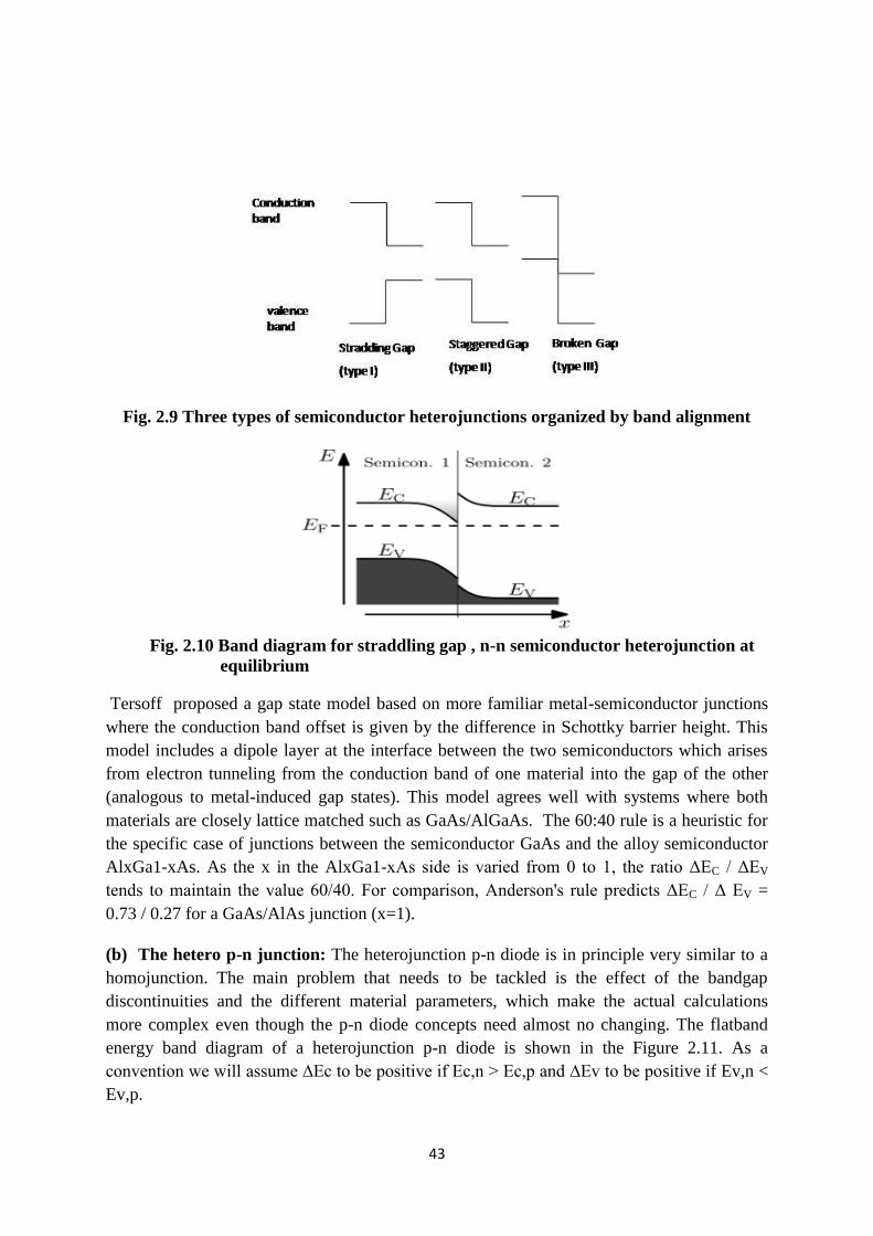
43
Fig. 2.9 Three types of semiconductor heterojunctions organized by band alignment
Fig. 2.10 Band diagram for straddling gap , n-n semiconductor heterojunction at
equilibrium
Tersoff proposed a gap state model based on more familiar metal-semiconductor junctions
where the conduction band offset is given by the difference in Schottky barrier height. This
model includes a dipole layer at the interface between the two semiconductors which arises
from electron tunneling from the conduction band of one material into the gap of the other
(analogous to metal-induced gap states). This model agrees well with systems where both
materials are closely lattice matched such as GaAs/AlGaAs. The 60:40 rule is a heuristic for
the specific case of junctions between the semiconductor GaAs and the alloy semiconductor
AlxGa1-xAs. As the x in the AlxGa1-xAs side is varied from 0 to 1, the ratio ΔEC / ΔEV
tends to maintain the value 60/40. For comparison, Anderson's rule predicts ΔEC / Δ EV =
0.73 / 0.27 for a GaAs/AlAs junction (x=1).
(b) The hetero p-n junction: The heterojunction p-n diode is in principle very similar to a
homojunction. The main problem that needs to be tackled is the effect of the bandgap
discontinuities and the different material parameters, which make the actual calculations
more complex even though the p-n diode concepts need almost no changing. The flatband
energy band diagram of a heterojunction p-n diode is shown in the Figure 2.11. As a
convention we will assume ∆Ec to be positive if Ec,n > Ec,p and ∆Ev to be positive if Ev,n <
Ev,p.
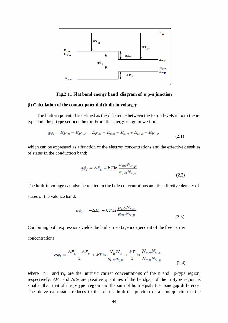
44
Fig.2.11 Flat band energy band diagram of a p-n junction
(i) Calculation of the contact potential (built-in voltage):
The built-in potential is defined as the difference between the Fermi levels in both the n-
type and the p-type semiconductor. From the energy diagram we find:
(2.1)
which can be expressed as a function of the electron concentrations and the effective densities
of states in the conduction band:
(2.2)
The built-in voltage can also be related to the hole concentrations and the effective density of
states of the valence band:
(2.3)
Combining both expressions yields the built-in voltage independent of the free carrier
concentrations:
(2.4)
where nin and nip are the intrinsic carrier concentrations of the n and p-type region,
respectively. ∆Ec and ∆Ev are positive quantities if the bandgap of the n-type region is
smaller than that of the p-type region and the sum of both equals the bandgap difference.
The above expression reduces to that of the built-in junction of a homojunction if the
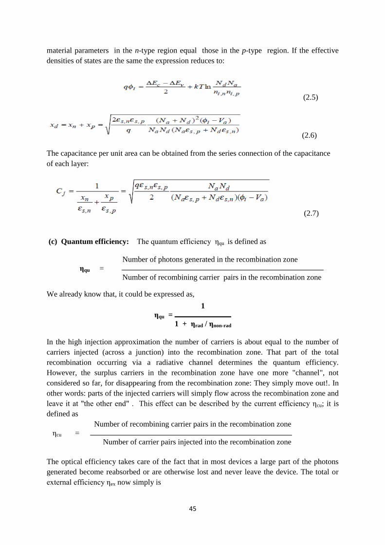
45
material parameters in the n-type region equal those in the p-type region. If the effective
densities of states are the same the expression reduces to:
(2.5)
(2.6)
The capacitance per unit area can be obtained from the series connection of the capacitance
of each layer:
(2.7)
(c) Quantum efficiency: The quantum efficiency ηqu is defined as
Number of photons generated in the recombination zone
ηqu =
Number of recombining carrier pairs in the recombination zone
We already know that, it could be expressed as,
ηqu =
1
1 + ηrad / ηnon-rad
In the high injection approximation the number of carriers is about equal to the number of
carriers injected (across a junction) into the recombination zone. That part of the total
recombination occurring via a radiative channel determines the quantum efficiency.
However, the surplus carriers in the recombination zone have one more "channel", not
considered so far, for disappearing from the recombination zone: They simply move out!. In
other words: parts of the injected carriers will simply flow across the recombination zone and
leave it at "the other end" . This effect can be described by the current efficiency ηcu; it is
defined as
Number of recombining carrier pairs in the recombination zone
ηcu =
Number of carrier pairs injected into the recombination zone
The optical efficiency takes care of the fact that in most devices a large part of the photons
generated become reabsorbed or are otherwise lost and never leave the device. The total or
external efficiency ηex now simply is
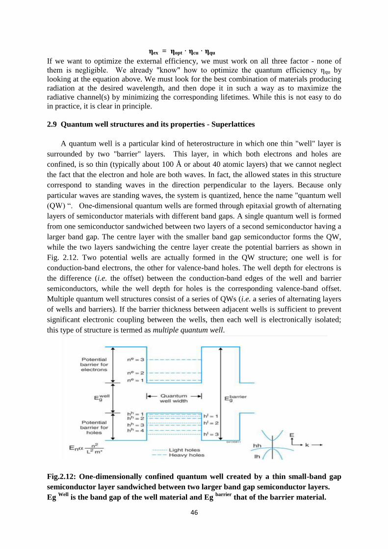
46
ηex = ηopt · ηcu · ηqu
If we want to optimize the external efficiency, we must work on all three factor - none of
them is negligible. We already "know" how to optimize the quantum efficiency ηqu by
looking at the equation above. We must look for the best combination of materials producing
radiation at the desired wavelength, and then dope it in such a way as to maximize the
radiative channel(s) by minimizing the corresponding lifetimes. While this is not easy to do
in practice, it is clear in principle.
2.9 Quantum well structures and its properties - Superlattices
A quantum well is a particular kind of heterostructure in which one thin "well" layer is
surrounded by two "barrier" layers. This layer, in which both electrons and holes are
confined, is so thin (typically about 100 Å or about 40 atomic layers) that we cannot neglect
the fact that the electron and hole are both waves. In fact, the allowed states in this structure
correspond to standing waves in the direction perpendicular to the layers. Because only
particular waves are standing waves, the system is quantized, hence the name "quantum well
(QW) “. One-dimensional quantum wells are formed through epitaxial growth of alternating
layers of semiconductor materials with different band gaps. A single quantum well is formed
from one semiconductor sandwiched between two layers of a second semiconductor having a
larger band gap. The centre layer with the smaller band gap semiconductor forms the QW,
while the two layers sandwiching the centre layer create the potential barriers as shown in
Fig. 2.12. Two potential wells are actually formed in the QW structure; one well is for
conduction-band electrons, the other for valence-band holes. The well depth for electrons is
the difference (i.e. the offset) between the conduction-band edges of the well and barrier
semiconductors, while the well depth for holes is the corresponding valence-band offset.
Multiple quantum well structures consist of a series of QWs (i.e. a series of alternating layers
of wells and barriers). If the barrier thickness between adjacent wells is sufficient to prevent
significant electronic coupling between the wells, then each well is electronically isolated;
this type of structure is termed as multiple quantum well.
Fig.2.12: One-dimensionally confined quantum well created by a thin small-band gap
semiconductor layer sandwiched between two larger band gap semiconductor layers.
Eg Well
is the band gap of the well material and Eg barrier
that of the barrier material.
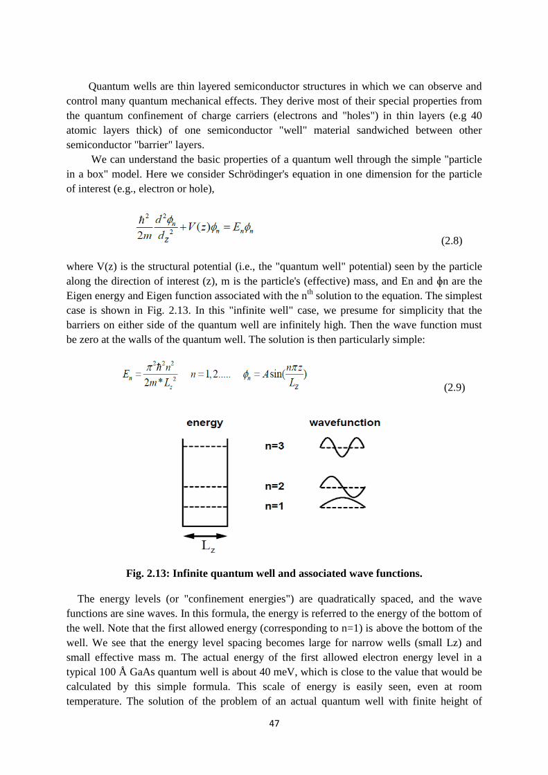
47
Quantum wells are thin layered semiconductor structures in which we can observe and
control many quantum mechanical effects. They derive most of their special properties from
the quantum confinement of charge carriers (electrons and "holes") in thin layers (e.g 40
atomic layers thick) of one semiconductor "well" material sandwiched between other
semiconductor "barrier" layers.
We can understand the basic properties of a quantum well through the simple "particle
in a box" model. Here we consider Schrödinger's equation in one dimension for the particle
of interest (e.g., electron or hole),
(2.8)
where V(z) is the structural potential (i.e., the "quantum well" potential) seen by the particle
along the direction of interest (z), m is the particle's (effective) mass, and En and ɸn are the
Eigen energy and Eigen function associated with the nth
solution to the equation. The simplest
case is shown in Fig. 2.13. In this "infinite well" case, we presume for simplicity that the
barriers on either side of the quantum well are infinitely high. Then the wave function must
be zero at the walls of the quantum well. The solution is then particularly simple:
(2.9)
Fig. 2.13: Infinite quantum well and associated wave functions.
The energy levels (or "confinement energies") are quadratically spaced, and the wave
functions are sine waves. In this formula, the energy is referred to the energy of the bottom of
the well. Note that the first allowed energy (corresponding to n=1) is above the bottom of the
well. We see that the energy level spacing becomes large for narrow wells (small Lz) and
small effective mass m. The actual energy of the first allowed electron energy level in a
typical 100 Å GaAs quantum well is about 40 meV, which is close to the value that would be
calculated by this simple formula. This scale of energy is easily seen, even at room
temperature. The solution of the problem of an actual quantum well with finite height of
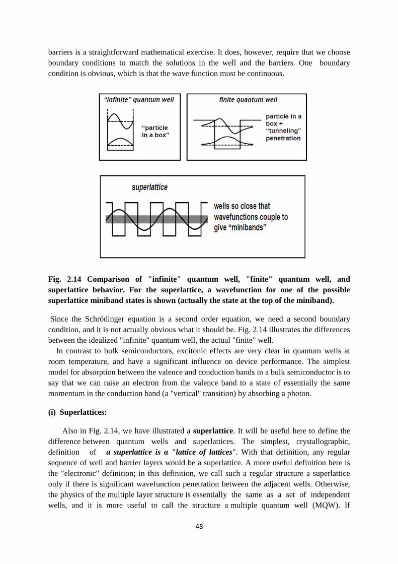
48
barriers is a straightforward mathematical exercise. It does, however, require that we choose
boundary conditions to match the solutions in the well and the barriers. One boundary
condition is obvious, which is that the wave function must be continuous.
Fig. 2.14 Comparison of "infinite" quantum well, "finite" quantum well, and
superlattice behavior. For the superlattice, a wavefunction for one of the possible
superlattice miniband states is shown (actually the state at the top of the miniband).
Since the Schrödinger equation is a second order equation, we need a second boundary
condition, and it is not actually obvious what it should be. Fig. 2.14 illustrates the differences
between the idealized "infinite" quantum well, the actual "finite" well.
In contrast to bulk semiconductors, excitonic effects are very clear in quantum wells at
room temperature, and have a significant influence on device performance. The simplest
model for absorption between the valence and conduction bands in a bulk semiconductor is to
say that we can raise an electron from the valence band to a state of essentially the same
momentum in the conduction band (a "vertical" transition) by absorbing a photon.
(i) Superlattices:
Also in Fig. 2.14, we have illustrated a superlattice. It will be useful here to define the
difference between quantum wells and superlattices. The simplest, crystallographic,
definition of a superlattice is a "lattice of lattices". With that definition, any regular
sequence of well and barrier layers would be a superlattice. A more useful definition here is
the "electronic" definition; in this definition, we call such a regular structure a superlattice
only if there is significant wavefunction penetration between the adjacent wells. Otherwise,
the physics of the multiple layer structure is essentially the same as a set of independent
wells, and it is more useful to call the structure a multiple quantum well (MQW). If
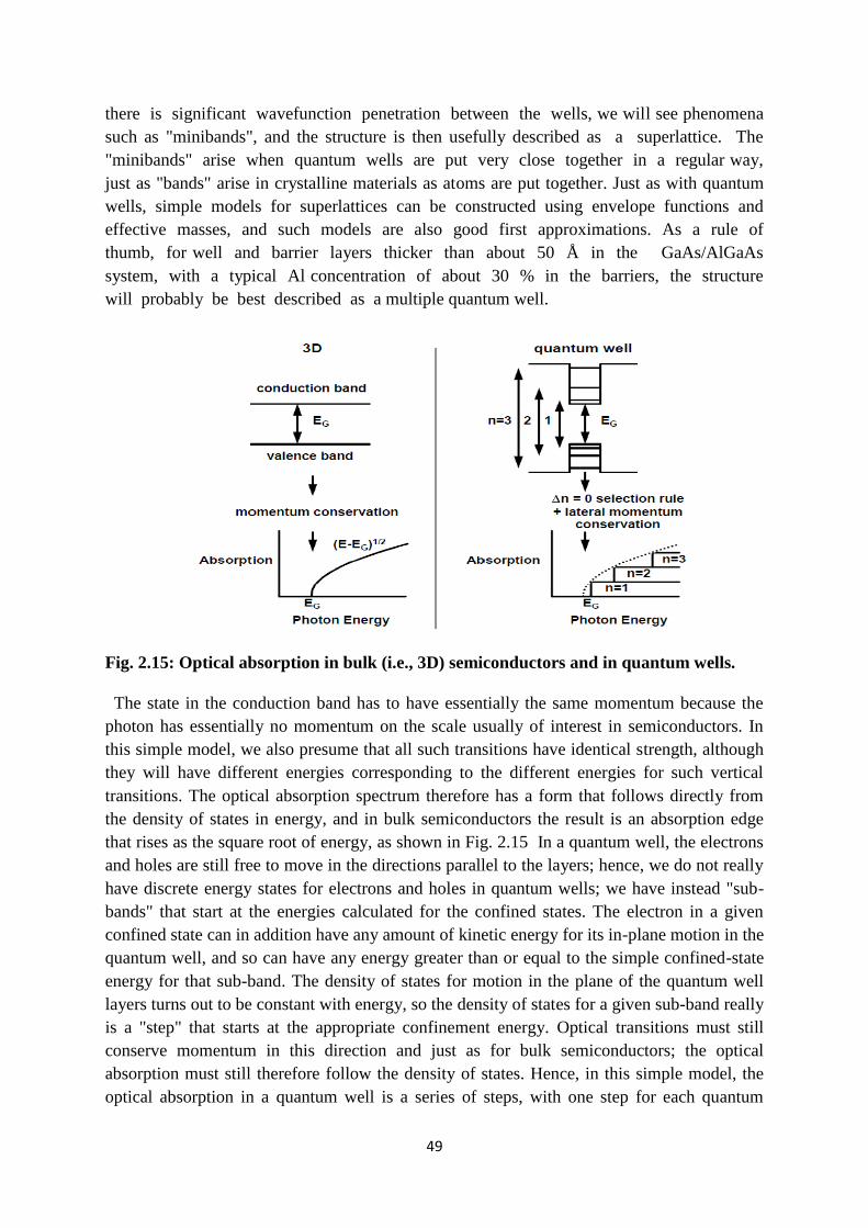
49
there is significant wavefunction penetration between the wells, we will see phenomena
such as "minibands", and the structure is then usefully described as a superlattice. The
"minibands" arise when quantum wells are put very close together in a regular way,
just as "bands" arise in crystalline materials as atoms are put together. Just as with quantum
wells, simple models for superlattices can be constructed using envelope functions and
effective masses, and such models are also good first approximations. As a rule of
thumb, for well and barrier layers thicker than about 50 Å in the GaAs/AlGaAs
system, with a typical Al concentration of about 30 % in the barriers, the structure
will probably be best described as a multiple quantum well.
Fig. 2.15: Optical absorption in bulk (i.e., 3D) semiconductors and in quantum wells.
The state in the conduction band has to have essentially the same momentum because the
photon has essentially no momentum on the scale usually of interest in semiconductors. In
this simple model, we also presume that all such transitions have identical strength, although
they will have different energies corresponding to the different energies for such vertical
transitions. The optical absorption spectrum therefore has a form that follows directly from
the density of states in energy, and in bulk semiconductors the result is an absorption edge
that rises as the square root of energy, as shown in Fig. 2.15 In a quantum well, the electrons
and holes are still free to move in the directions parallel to the layers; hence, we do not really
have discrete energy states for electrons and holes in quantum wells; we have instead "sub-
bands" that start at the energies calculated for the confined states. The electron in a given
confined state can in addition have any amount of kinetic energy for its in-plane motion in the
quantum well, and so can have any energy greater than or equal to the simple confined-state
energy for that sub-band. The density of states for motion in the plane of the quantum well
layers turns out to be constant with energy, so the density of states for a given sub-band really
is a "step" that starts at the appropriate confinement energy. Optical transitions must still
conserve momentum in this direction and just as for bulk semiconductors; the optical
absorption must still therefore follow the density of states. Hence, in this simple model, the
optical absorption in a quantum well is a series of steps, with one step for each quantum
50
number, n. It is easily shown, from the known densities of states, that the corners of the steps
"touch" the square root bulk absorption curve (when that curve is scaled to the thickness of
this infinite quantum well). Thus, as we imagine increasing the quantum well thickness, we
will make a smooth transition to the bulk behaviour, with the steps becoming increasingly
close until they merge into the continuous absorption edge of the bulk material.
(ii) Fabrication: Quantum wells are formed in semiconductors by having a material, like
gallium arsenide, sandwiched between two layers of a material with a wider bandgap, like
aluminium arsenide. (Other example: layer of indium gallium nitride sandwiched between
two layers of gallium nitride.) These structures can be grown by molecular beam epitaxy or
chemical vapor deposition with control of the layer thickness down to monolayers. Thin
metal films can also support quantum well states, in particular, metallic thin overlayers grown
in metal and semiconductor surfaces. The electron (or hole) is confined by the vacuum-metal
interface in one side, and in general, by an absolute gap with semiconductor substrates, or by
a projected band gap with metal substrates.
(iii) Applications: Because of their quasi-two dimensional nature, electrons in quantum
wells have a density of states as a function of energy that has distinct steps, versus a smooth
square root dependence that is found in bulk materials. Additionally, the effective mass of
holes in the valence band is changed to more closely match that of electrons in the conduction
band. These two factors, together with the reduced amount of active material in quantum
wells, leads to better performance in optical devices such as laser diodes. As a result quantum
wells are in wide use in diode lasers, including red lasers for DVDs and laser pointers, infra-
red lasers in fiber optic transmitters, or in blue lasers. They are also used to make HEMTs
(High Electron Mobility Transistors), which are used in low-noise electronics. Quantum well
infrared photodetectors are also based on quantum wells, and are used for infrared imaging.
By doping either the well itself, or preferably, the barrier of a quantum well with donor
impurities, a two-dimensional electron gas (2DEG) may be formed. Such a structure forms
the conducting channel of a HEMT, and has interesting properties at low temperature. One
such property is the quantum Hall effect, seen at high magnetic fields. Acceptor dopants can
also lead to a two-dimensional hole gas (2DHG).
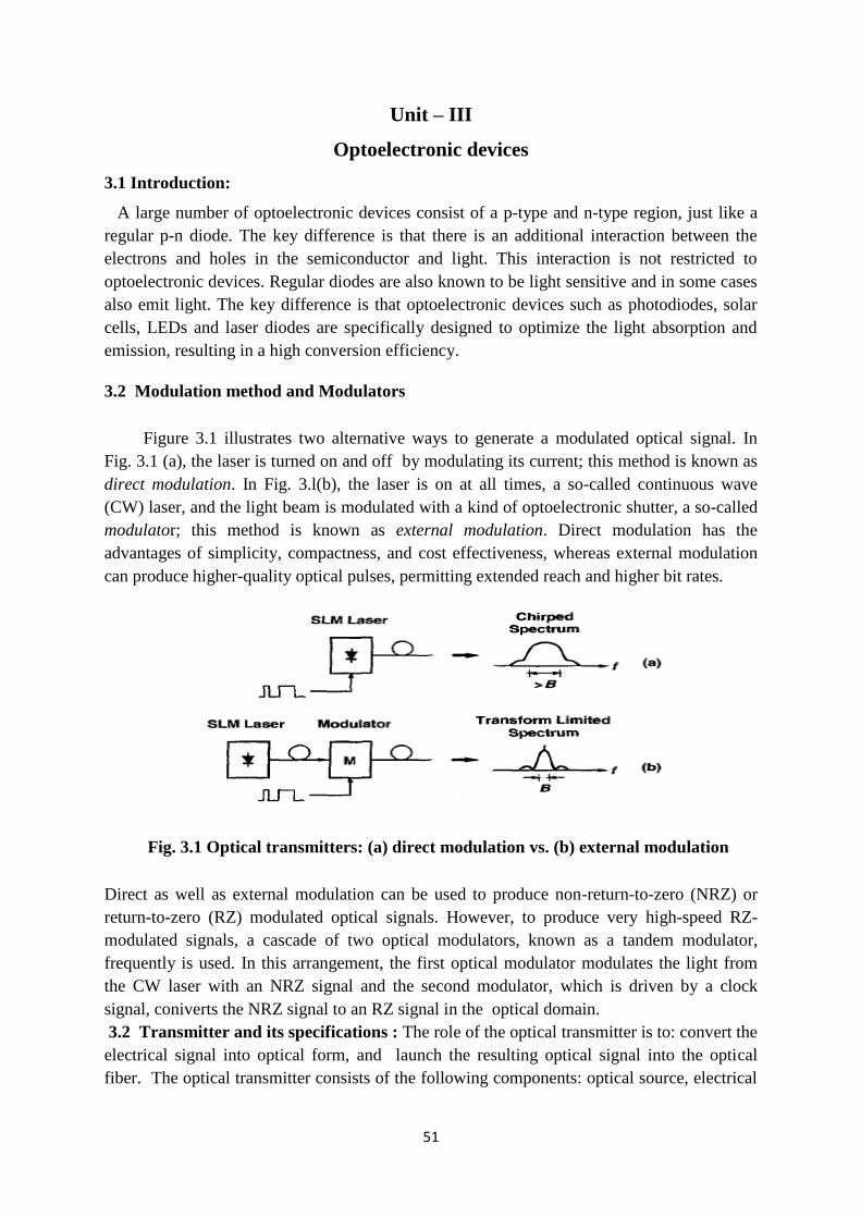
51
Unit – III
Optoelectronic devices
3.1 Introduction:
A large number of optoelectronic devices consist of a p-type and n-type region, just like a
regular p-n diode. The key difference is that there is an additional interaction between the
electrons and holes in the semiconductor and light. This interaction is not restricted to
optoelectronic devices. Regular diodes are also known to be light sensitive and in some cases
also emit light. The key difference is that optoelectronic devices such as photodiodes, solar
cells, LEDs and laser diodes are specifically designed to optimize the light absorption and
emission, resulting in a high conversion efficiency.
3.2 Modulation method and Modulators
Figure 3.1 illustrates two alternative ways to generate a modulated optical signal. In
Fig. 3.1 (a), the laser is turned on and off by modulating its current; this method is known as
direct modulation. In Fig. 3.l(b), the laser is on at all times, a so-called continuous wave
(CW) laser, and the light beam is modulated with a kind of optoelectronic shutter, a so-called
modulator; this method is known as external modulation. Direct modulation has the
advantages of simplicity, compactness, and cost effectiveness, whereas external modulation
can produce higher-quality optical pulses, permitting extended reach and higher bit rates.
Fig. 3.1 Optical transmitters: (a) direct modulation vs. (b) external modulation
Direct as well as external modulation can be used to produce non-return-to-zero (NRZ) or
return-to-zero (RZ) modulated optical signals. However, to produce very high-speed RZ-
modulated signals, a cascade of two optical modulators, known as a tandem modulator,
frequently is used. In this arrangement, the first optical modulator modulates the light from
the CW laser with an NRZ signal and the second modulator, which is driven by a clock
signal, coniverts the NRZ signal to an RZ signal in the optical domain.
3.2 Transmitter and its specifications : The role of the optical transmitter is to: convert the
electrical signal into optical form, and launch the resulting optical signal into the optical
fiber. The optical transmitter consists of the following components: optical source, electrical
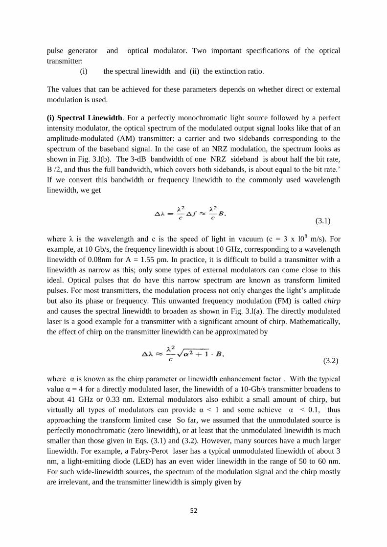
52
pulse generator and optical modulator. Two important specifications of the optical
transmitter:
(i) the spectral linewidth and (ii) the extinction ratio.
The values that can be achieved for these parameters depends on whether direct or external
modulation is used.
(i) Spectral Linewidth. For a perfectly monochromatic light source followed by a perfect
intensity modulator, the optical spectrum of the modulated output signal looks like that of an
amplitude-modulated (AM) transmitter: a carrier and two sidebands corresponding to the
spectrum of the baseband signal. In the case of an NRZ modulation, the spectrum looks as
shown in Fig. 3.l(b). The 3-dB bandwidth of one NRZ sideband is about half the bit rate,
B /2, and thus the full bandwidth, which covers both sidebands, is about equal to the bit rate.’
If we convert this bandwidth or frequency linewidth to the commonly used wavelength
linewidth, we get
(3.1)
where λ is the wavelength and c is the speed of light in vacuum (c = 3 x l08 m/s). For
example, at 10 Gb/s, the frequency linewidth is about 10 GHz, corresponding to a wavelength
linewidth of 0.08nm for A = 1.55 pm. In practice, it is difficult to build a transmitter with a
linewidth as narrow as this; only some types of external modulators can come close to this
ideal. Optical pulses that do have this narrow spectrum are known as transform limited
pulses. For most transmitters, the modulation process not only changes the light’s amplitude
but also its phase or frequency. This unwanted frequency modulation (FM) is called chirp
and causes the spectral linewidth to broaden as shown in Fig. 3.l(a). The directly modulated
laser is a good example for a transmitter with a significant amount of chirp. Mathematically,
the effect of chirp on the transmitter linewidth can be approximated by
(3.2)
where α is known as the chirp parameter or linewidth enhancement factor . With the typical
value α = 4 for a directly modulated laser, the linewidth of a 10-Gb/s transmitter broadens to
about 41 GHz or 0.33 nm. External modulators also exhibit a small amount of chirp, but
virtually all types of modulators can provide α < 1 and some achieve α < 0.1, thus
approaching the transform limited case So far, we assumed that the unmodulated source is
perfectly monochromatic (zero linewidth), or at least that the unmodulated linewidth is much
smaller than those given in Eqs. (3.1) and (3.2). However, many sources have a much larger
linewidth. For example, a Fabry-Perot laser has a typical unmodulated linewidth of about 3
nm, a light-emitting diode (LED) has an even wider linewidth in the range of 50 to 60 nm.
For such wide-linewidth sources, the spectrum of the modulation signal and the chirp mostly
are irrelevant, and the transmitter linewidth is simply given by
53
∆λ = ∆λ s (3.3)
where ΔλS is the linewidth of the unmodulated source.
(ii) Extinction Ratio. Optical transmitters, no matter if directly or externally modulated, do
not shut off completely when a zero is transmitted. This undesired effect quantified by the
extinction ratio (ER), which is defined as follows:
(3.4)
where PO is the optical power emitted for a zero and P1 the power for a one. Thus, an ideal
transmitter would have an infinite ER. The ER usually is expressed in dBs using the
conversion rule 10 log ER. Typically, ERs for directly modulated lasers range from 9 to 14
dB, whereas ERs for externally modulated lasers can exceed 15 dB . SONET / KDH transmitters
typically are required to have an ER in the range of 8.2 to 10 dB, depending on the
application. It doesn't come as a surprise that a finite ER causes a power penalty. Figure
3.2(a) and (b) illustrates how decreasing the ER reduces the optical signal swing, P1 - PO,
even if the average power = (PI + P0)/2 is kept constant. To restore the original signal swing,
we have to increase the average transmitted power, as shown in Fig. 3.2(c). The power
penalty PP due to a finite extinction ratio can easily be derived as
(3.5)
For example, an extinction ratio of 10 dB (ER = 10) causes a power penalty of 0.87dB (PP =
1.22).
Fjg, 3.2 Eye diagram (a) with infinite ER, (b) with ER = 5, and (c) with ER = 5 and
increased average power (1.5 x ) to restore the original signal swing.
In deriving Eq. (3.5), it was assumed that the ER does not affect the amount of noise at the
receiver. This is the case for unamplified p-i-n receivers; however, in systems with an
avalanche photodetector (APD) or optical amplifiers, the noise increases when the ER is
reduced: (i) the nonzero value of PO adds noise on the zeros and (ii) the increase in power to
compensate for the finite ER adds noise on the zeros and ones, necessitating an even larger
power increase to compensate for this noise. As a result of these two mechanisms, the power
penalty becomes larger than given in Eq. (3.5). If we take the extreme case where the:
receiver noise is dominated by the detector (or optical amplifier) noise such that the electrical
noise power is proportional to the received signal current, we find that
54
(3.6)
For example, an extinction ratio of 10 clB (ER = 10) causes a power penalty of up to 3.72dB
(PP = 2.35) in an amplified lightwave systems. In regulatory standards, the receiver
sensitivity usually is specified for the worst- case extinction ratio. Therefore, the
corresponding power penalty must be deducted from the sensitivity based on ER + 00.
Typically, 2.2 dB (for ER = 6 dB) must be deducted in short-haul applications, and 0.87 dB
(for ER = 10 dB) must be deducted in long-haul applications. Instead of specifying the
average transmitter power, the optical modulation amplitude (OMA), which is defined as PJ -
PO and measured in dBm, can be used to measure the transmitter power. The OMA measure
is used, for example, in 10-GbE systems. If the transmitter power and the receiver sensitivity
are specified in terms of OMA rather than average power, a finite extinction ratio causes
much less of a power penalty (no power penalty in the case of constant noise).
3.3 Light Emitting Diode:
A light-emitting diode (LED) is a semiconductor device that emits visible light when an
electric current passes through it. The light is not particularly bright, but in most LEDs it is
monochromatic, occurring at a single wavelength. The output from an LED can range from
red (at a wavelength of approximately 700 nanometers) to blue-violet (about 400
nanometers). Some LEDs emit infrared (IR) energy (830 nanometers or longer); such a
device is known as an infrared-emitting diode (IRED). An LED or IRED consists of two
elements of processed material called P-type semiconductors and N-type semiconductors.
These two elements are placed in direct contact, forming a region called the P-N junction. In
this respect, the LED or IRED resembles most other diode types, but there are important
differences. The LED or IRED has a transparent package, allowing visible or IR energy to
pass through. Also, the LED or IRED has a large PN-junction area whose shape is tailored to
the application.
3.4 Advantages and Disadvantages of LEDs
The light emitting diodes (LEDs) are very simple devices as compared to laser diodes.
The advantages and disadvantages of LEDs are following:
Advantages:
Simple device. It is a simple device like p-n junction diode without any resonator mirrors and
complicated striped structure.
Low cost. It is an inexpensive optical source due to simple p-n junction device and is
ideally used with multimode fibres.
Reliability. The LEDs are reliable in performance and it does not degrade abruptly. It is
free from modal noise and is easy to handle.
Temperature dependence. It is just like a p-n junction diode and the variation of temperature
with current is linear. If the temperature of device is increased, its output may decrease but it
will not stop working. Thus, no cooling is required as compared to laser diode where
temperature rise an degrade laser power drastically.
Simple electronics. It uses simple device circuits for its working and no temperature
compensation circuits are needed. So, overall cost of electronics is also low.
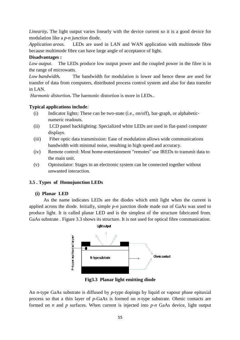
55
Linearity. The light output varies linearly with the device current so it is a good device for
modulation like a p-n junction diode.
Application areas. LEDs are used in LAN and WAN application with multimode fibre
because multimode fibre can have large angle of acceptance of light.
Disadvantages :
Low output. The LEDs produce low output power and the coupled power in the fibre is in
the range of microwatts.
Low bandwidth. The bandwidth for modulation is lower and hence these are used for
transfer of data from computers, distributed process control system and also for data transfer
in LAN.
Harmonic distortion. The harmonic distortion is more in LEDs..
Typical applications include:
(i) Indicator lights: These can be two-state (i.e., on/off), bar-graph, or alphabetic-
numeric readouts.
(ii) LCD panel backlighting: Specialized white LEDs are used in flat-panel computer
displays.
(iii) Fiber optic data transmission: Ease of modulation allows wide communications
bandwidth with minimal noise, resulting in high speed and accuracy.
(iv) Remote control: Most home-entertainment "remotes" use IREDs to transmit data to
the main unit.
(v) Optoisolator: Stages in an electronic system can be connected together without
unwanted interaction.
3.5 . Types of Homojunction LEDs
(i) Planar LED
As the name indicates LEDs are the diodes which emit light when the current is
applied across the diode. Initially, simple p-n junction diode made out of GaAs was used to
produce light. It is called planar LED and is the simplest of the structure fabricated from.
GaAs substrate . Figure 3.3 shows its structure. It is not used for optical fibre communication.
Fig3.3 Planar light emitting diode
An n-type GaAs substrate is diffused by p-type dopings by liquid or vapour phase epitaxial
process so that a thin layer of p-GaAs is formed on n-type substrate. Ohmic contacts are
formed on n and p surfaces. When current is injected into p-n GaAs device, light output
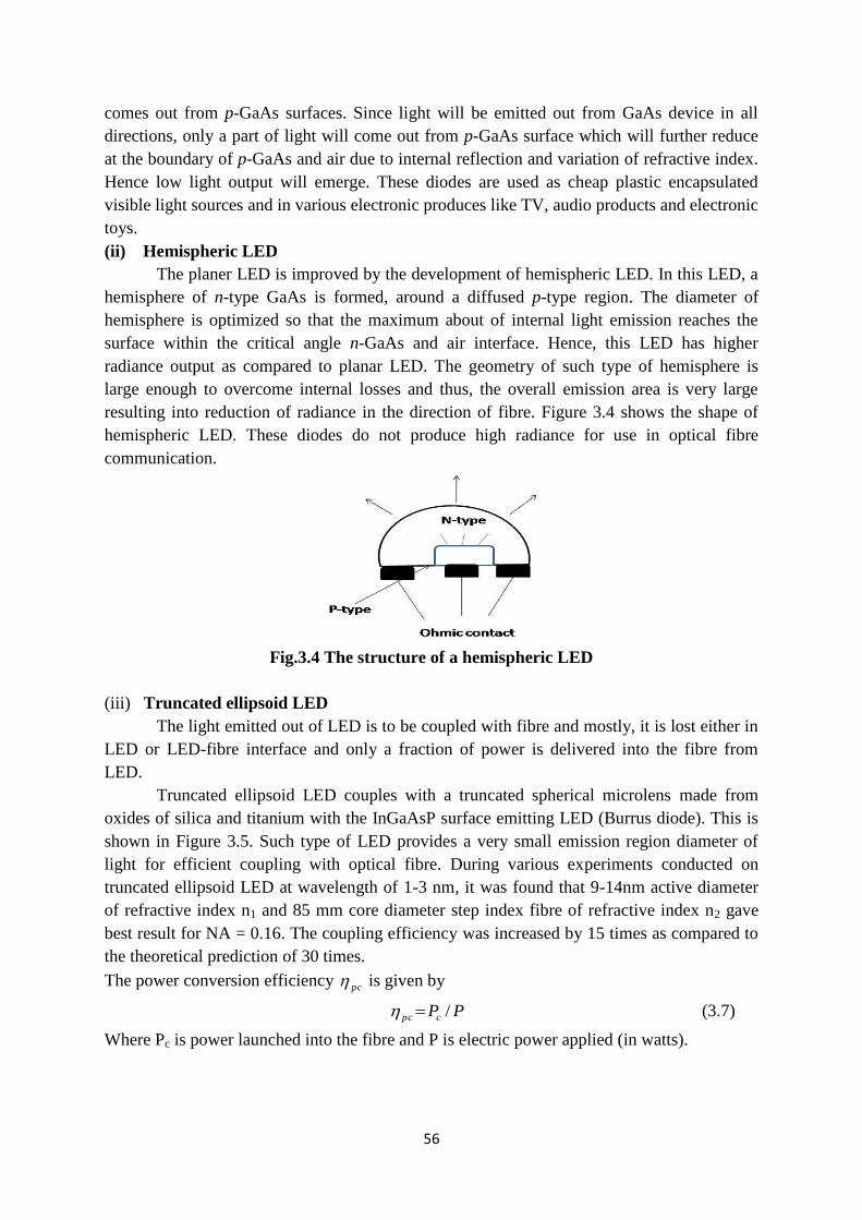
56
comes out from p-GaAs surfaces. Since light will be emitted out from GaAs device in all
directions, only a part of light will come out from p-GaAs surface which will further reduce
at the boundary of p-GaAs and air due to internal reflection and variation of refractive index.
Hence low light output will emerge. These diodes are used as cheap plastic encapsulated
visible light sources and in various electronic produces like TV, audio products and electronic
toys.
(ii) Hemispheric LED
The planer LED is improved by the development of hemispheric LED. In this LED, a
hemisphere of n-type GaAs is formed, around a diffused p-type region. The diameter of
hemisphere is optimized so that the maximum about of internal light emission reaches the
surface within the critical angle n-GaAs and air interface. Hence, this LED has higher
radiance output as compared to planar LED. The geometry of such type of hemisphere is
large enough to overcome internal losses and thus, the overall emission area is very large
resulting into reduction of radiance in the direction of fibre. Figure 3.4 shows the shape of
hemispheric LED. These diodes do not produce high radiance for use in optical fibre
communication.
Fig.3.4 The structure of a hemispheric LED
(iii) Truncated ellipsoid LED
The light emitted out of LED is to be coupled with fibre and mostly, it is lost either in
LED or LED-fibre interface and only a fraction of power is delivered into the fibre from
LED.
Truncated ellipsoid LED couples with a truncated spherical microlens made from
oxides of silica and titanium with the InGaAsP surface emitting LED (Burrus diode). This is
shown in Figure 3.5. Such type of LED provides a very small emission region diameter of
light for efficient coupling with optical fibre. During various experiments conducted on
truncated ellipsoid LED at wavelength of 1-3 nm, it was found that 9-14nm active diameter
of refractive index n1 and 85 mm core diameter step index fibre of refractive index n2 gave
best result for NA = 0.16. The coupling efficiency was increased by 15 times as compared to
the theoretical prediction of 30 times.
The power conversion efficiency pc is given by
PPcpc / (3.7)
Where Pc is power launched into the fibre and P is electric power applied (in watts).
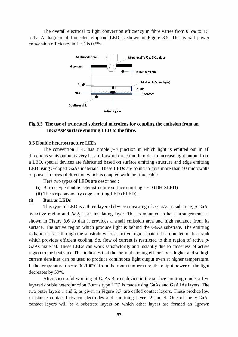
57
The overall electrical to light conversion efficiency in fibre varies from 0.5% to 1%
only. A diagram of truncated ellipsoid LED is shown in Figure 3.5. The overall power
conversion efficiency in LED is 0.5%.
Fig.3.5 The use of truncated spherical microlens for coupling the emission from an
InGaAsP surface emitting LED to the fibre.
3.5 Double heterostructure LEDs
The convention LED has simple p-n junction in which light is emitted out in all
directions so its output is very less in forward direction. In order to increase light output from
a LED, special devices are fabricated based on surface emitting structure and edge emitting
LED using n-doped GaAs materials. These LEDs are found to give more than 50 microwatts
of power in forward direction which is coupled with the fibre cable.
Here two types of LEDs are described :
(i) Burrus type double heterostructure surface emitting LED (DH-SLED)
(ii) The stripe geometry edge emitting LED (ELED).
(i) Burrus LEDs
This type of LED is a three-layered device consisting of n-GaAs as substrate, p-GaAs
as active region and 2SiO as an insulating layer. This is mounted in back arrangements as
shown in Figure 3.6 so that it provides a small emission area and high radiance from its
surface. The active region which produce light is behind the GaAs substrate. The emitting
radiation passes through the substrate whereas active region material is mounted on heat sink
which provides efficient cooling. So, flow of current is restricted to thin region of active p-
GaAs material. These LEDs can work satisfactorily and instantly due to closeness of active
region to the heat sink. This indicates that the thermal cooling efficiency is higher and so high
current densities can be used to produce continuous light output even at higher temperature.
If the temperature risesto 90-100C from the room temperature, the output power of the light
decreases by 50%.
After successful working of GaAs Burrus device in the surface emitting mode, a five
layered double heterojunction Burrus type LED is made using GaAs and GaA1As layers. The
two outer layers 1 and 5, as given in Figure 3.7, are called contact layers. These prodice low
resistance contact between electrodes and confining layers 2 and 4. One of the n-GaAs
contact layers will be a substrate layers on which other layers are formed an 1grown
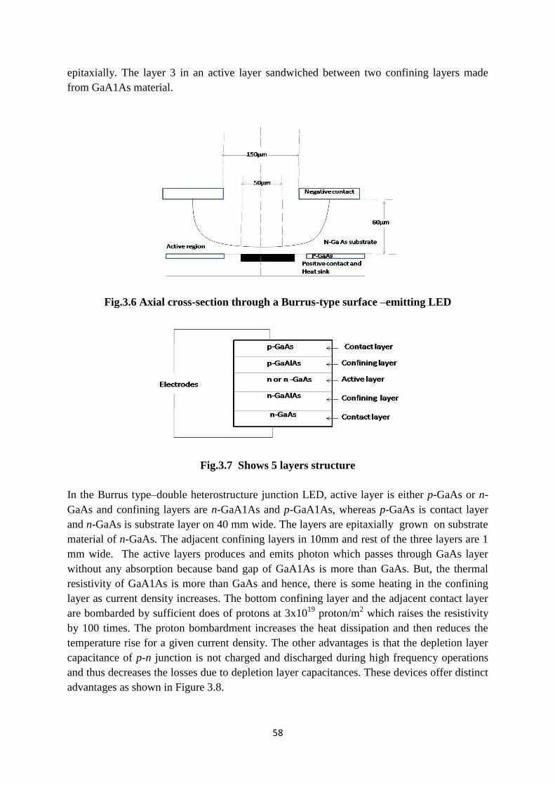
58
epitaxially. The layer 3 in an active layer sandwiched between two confining layers made
from GaA1As material.
Fig.3.6 Axial cross-section through a Burrus-type surface –emitting LED
Fig.3.7 Shows 5 layers structure
In the Burrus type–double heterostructure junction LED, active layer is either p-GaAs or n-
GaAs and confining layers are n-GaA1As and p-GaA1As, whereas p-GaAs is contact layer
and n-GaAs is substrate layer on 40 mm wide. The layers are epitaxially grown on substrate
material of n-GaAs. The adjacent confining layers in 10mm and rest of the three layers are 1
mm wide. The active layers produces and emits photon which passes through GaAs layer
without any absorption because band gap of GaA1As is more than GaAs. But, the thermal
resistivity of GaA1As is more than GaAs and hence, there is some heating in the confining
layer as current density increases. The bottom confining layer and the adjacent contact layer
are bombarded by sufficient does of protons at 3x10¹⁹
proton/m2 which raises the resistivity
by 100 times. The proton bombardment increases the heat dissipation and then reduces the
temperature rise for a given current density. The other advantages is that the depletion layer
capacitance of p-n junction is not charged and discharged during high frequency operations
and thus decreases the losses due to depletion layer capacitances. These devices offer distinct
advantages as shown in Figure 3.8.
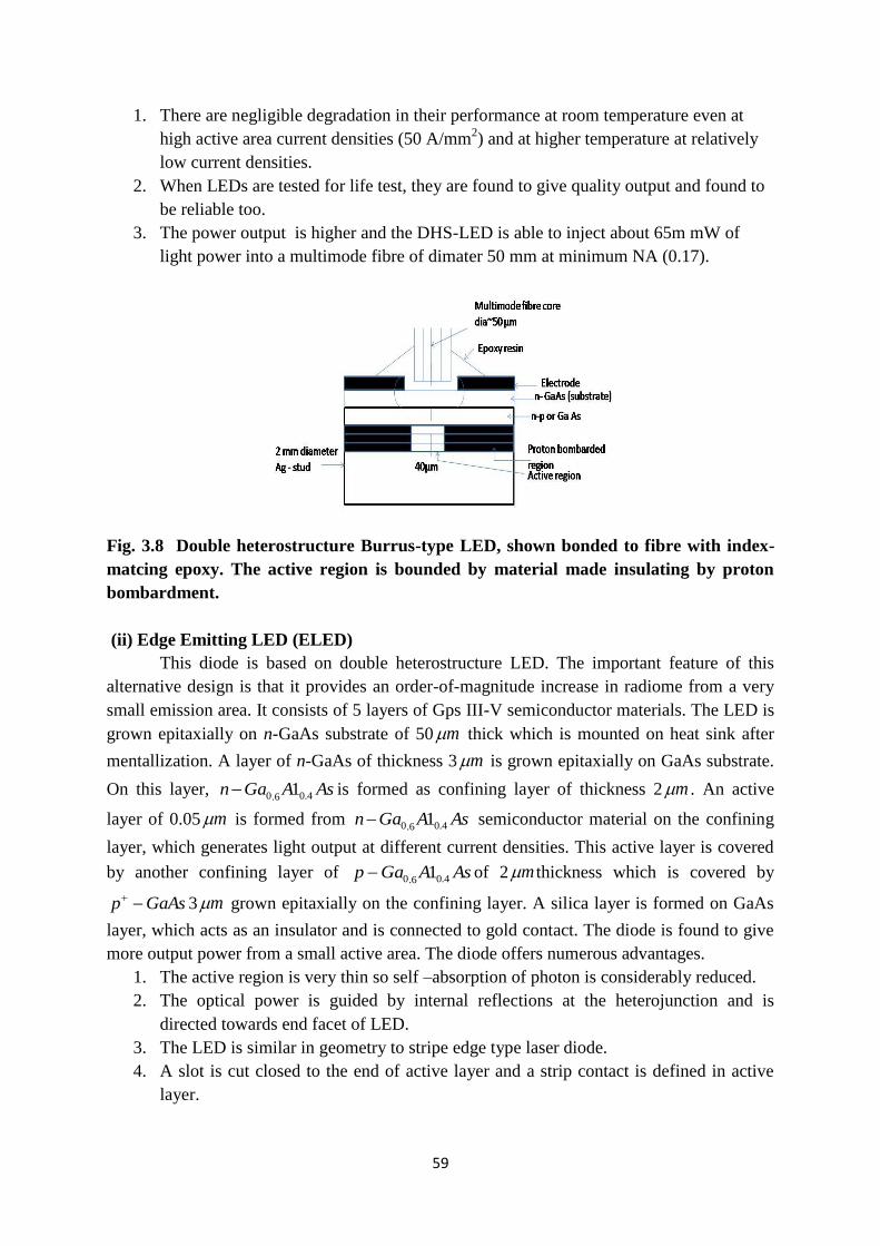
59
1. There are negligible degradation in their performance at room temperature even at
high active area current densities (50 A/mm2) and at higher temperature at relatively
low current densities.
2. When LEDs are tested for life test, they are found to give quality output and found to
be reliable too.
3. The power output is higher and the DHS-LED is able to inject about 65m mW of
light power into a multimode fibre of dimater 50 mm at minimum NA (0.17).
Fig. 3.8 Double heterostructure Burrus-type LED, shown bonded to fibre with index-
matcing epoxy. The active region is bounded by material made insulating by proton
bombardment.
(ii) Edge Emitting LED (ELED)
This diode is based on double heterostructure LED. The important feature of this
alternative design is that it provides an order-of-magnitude increase in radiome from a very
small emission area. It consists of 5 layers of Gps III-V semiconductor materials. The LED is
grown epitaxially on n-GaAs substrate of 50 m thick which is mounted on heat sink after
mentallization. A layer of n-GaAs of thickness 3 m is grown epitaxially on GaAs substrate.
On this layer, AsAGan 4.06.0 1 is formed as confining layer of thickness 2 m . An active
layer of 0.05 m is formed from AsAGan 4.06.0 1 semiconductor material on the confining
layer, which generates light output at different current densities. This active layer is covered
by another confining layer of AsAGap 4.06.0 1 of 2 m thickness which is covered by
GaAsp 3 m grown epitaxially on the confining layer. A silica layer is formed on GaAs
layer, which acts as an insulator and is connected to gold contact. The diode is found to give
more output power from a small active area. The diode offers numerous advantages.
1. The active region is very thin so self –absorption of photon is considerably reduced.
2. The optical power is guided by internal reflections at the heterojunction and is
directed towards end facet of LED.
3. The LED is similar in geometry to stripe edge type laser diode.
4. A slot is cut closed to the end of active layer and a strip contact is defined in active
layer.
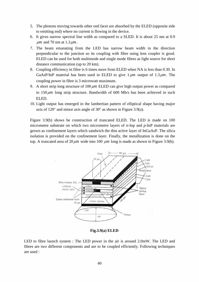
60
5. The photons moving towards other end facet are absorbed by the ELED (opposite side
to emitting end) where no current is flowing in the device.
6. It gives narrow spectral line width as compared to a SLED. It is about 25 nm at 0.9
m and 70 nm at 1.3 m .
7. The beam emanating from the LED has narrow beam width in the direction
perpendicular to the junction so its coupling with fibre using lens coupler is good.
ELED can be used for both multimode and single mode fibres as light source for short
distance communication (up to 20 km).
8. Coupling efficiency in fibre is 6 times more from ELED when NA is less than 0.30. In
GaAsP/InP material has been used in ELED to give 1 m output of 1.3 m . The
coupling power in fibre is 3 microwatt maximum.
9. A short strip long structure of 100 m ELED can give high output power as compared
to 150 m long strip structure. Bandwidth of 600 Mb/s has been achieved in such
ELED.
10. Light output has emerged in the lambertian pattern of elliptical shape having major
axis of 120 and minor axis angle of 30 as shown in Figure 3.9(a).
Figure 3.9(b) shows be construction of truncated ELED. The LED is made on 100
micrometre substrate on which two micrometre layers of n-Inp and p-InP materials are
grown as confinement layers which sandwich the thin active layer of InGaAsP. The silica
isolation is provided on the confinement layer. Finally, the metallization is done on the
top. A truncated area of 20 m wide into 100 m long is made as shown in Figure 3.9(b).
Fig.3.9(a) ELED
LED to fibre launch system : The LED power in the air is around 2.0mW. The LED and
fibres are two different components and are to be coupled efficiently. Following techniques
are used :
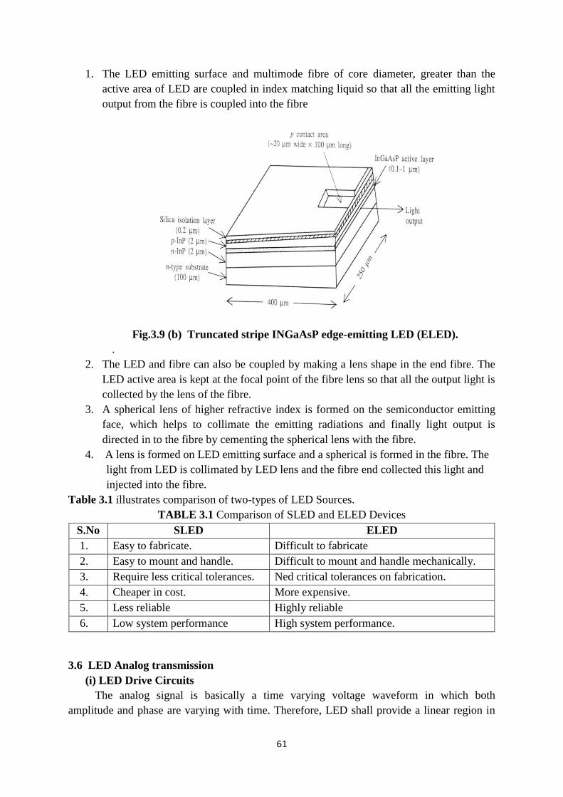
61
1. The LED emitting surface and multimode fibre of core diameter, greater than the
active area of LED are coupled in index matching liquid so that all the emitting light
output from the fibre is coupled into the fibre
Fig.3.9 (b) Truncated stripe INGaAsP edge-emitting LED (ELED).
.
2. The LED and fibre can also be coupled by making a lens shape in the end fibre. The
LED active area is kept at the focal point of the fibre lens so that all the output light is
collected by the lens of the fibre.
3. A spherical lens of higher refractive index is formed on the semiconductor emitting
face, which helps to collimate the emitting radiations and finally light output is
directed in to the fibre by cementing the spherical lens with the fibre.
4. A lens is formed on LED emitting surface and a spherical is formed in the fibre. The
light from LED is collimated by LED lens and the fibre end collected this light and
injected into the fibre.
Table 3.1 illustrates comparison of two-types of LED Sources.
TABLE 3.1 Comparison of SLED and ELED Devices
S.No SLED ELED
1. Easy to fabricate. Difficult to fabricate
2. Easy to mount and handle. Difficult to mount and handle mechanically.
3. Require less critical tolerances. Ned critical tolerances on fabrication.
4. Cheaper in cost. More expensive.
5. Less reliable Highly reliable
6. Low system performance High system performance.
3.6 LED Analog transmission
(i) LED Drive Circuits
The analog signal is basically a time varying voltage waveform in which both
amplitude and phase are varying with time. Therefore, LED shall provide a linear region in
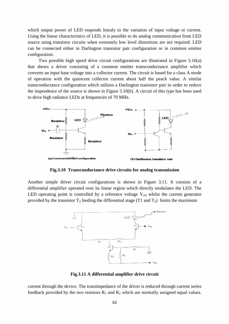
62
which output power of LED responds linealy to the variation of input voltage or current.
Using the linear characteristics of LED, it is possible to do analog communication from LED
source using transistor circuits when extremely low level distortions are not required. LED
can be connected either in Darlington transistor pair configuration or in common emitter
configuration.
Two possible high speed drive circuit configurations are illustrated in Figure 3.10(a)
that shows a driver consisting of a common emitter transconductance amplifier which
converts an input base voltage into a collector current. The circuit is based for a class A mode
of operation with the quiescent collector current about half the peack value. A similar
transconductance configuration which utilizes a Darlington transistor pair in order to reduce
the impendence of the source is shown in Figure 3.10(b). A circuit of this type has been used
to drive high radiance LEDs at frequencies of 70 MHz.
Fig.3.10 Transconductance drive circuits for analog transmission
Another simple driver circuit configurations is shown in Figure 3.11. It consists of a
differential amplifier operated over its linear region which directly modulates the LED. The
LED operating point is controlled by a reference voltage Vref whilst the current generator
provided by the transistor T3 feeding the differential stage (T1 and T2) limits the maximum
Fig.3.11 A differential amplifier drive circuit
current through the device. The transimpedance of the driver is reduced through current series
feedback provided by the two resistors R1 and R2 which are normally assigned equal values.
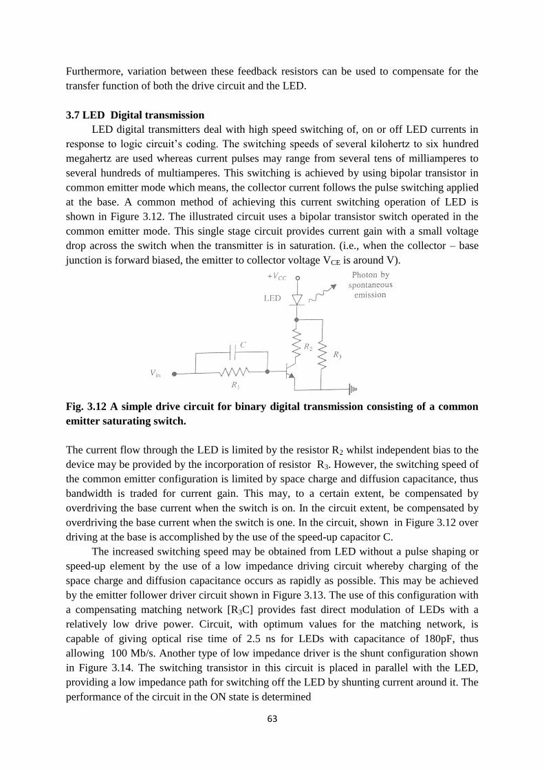
63
Furthermore, variation between these feedback resistors can be used to compensate for the
transfer function of both the drive circuit and the LED.
3.7 LED Digital transmission
LED digital transmitters deal with high speed switching of, on or off LED currents in
response to logic circuit’s coding. The switching speeds of several kilohertz to six hundred
megahertz are used whereas current pulses may range from several tens of milliamperes to
several hundreds of multiamperes. This switching is achieved by using bipolar transistor in
common emitter mode which means, the collector current follows the pulse switching applied
at the base. A common method of achieving this current switching operation of LED is
shown in Figure 3.12. The illustrated circuit uses a bipolar transistor switch operated in the
common emitter mode. This single stage circuit provides current gain with a small voltage
drop across the switch when the transmitter is in saturation. (i.e., when the collector – base
junction is forward biased, the emitter to collector voltage VCE is around V).
Fig. 3.12 A simple drive circuit for binary digital transmission consisting of a common
emitter saturating switch.
The current flow through the LED is limited by the resistor R2 whilst independent bias to the
device may be provided by the incorporation of resistor R3. However, the switching speed of
the common emitter configuration is limited by space charge and diffusion capacitance, thus
bandwidth is traded for current gain. This may, to a certain extent, be compensated by
overdriving the base current when the switch is on. In the circuit extent, be compensated by
overdriving the base current when the switch is one. In the circuit, shown in Figure 3.12 over
driving at the base is accomplished by the use of the speed-up capacitor C.
The increased switching speed may be obtained from LED without a pulse shaping or
speed-up element by the use of a low impedance driving circuit whereby charging of the
space charge and diffusion capacitance occurs as rapidly as possible. This may be achieved
by the emitter follower driver circuit shown in Figure 3.13. The use of this configuration with
a compensating matching network [R3C] provides fast direct modulation of LEDs with a
relatively low drive power. Circuit, with optimum values for the matching network, is
capable of giving optical rise time of 2.5 ns for LEDs with capacitance of 180pF, thus
allowing 100 Mb/s. Another type of low impedance driver is the shunt configuration shown
in Figure 3.14. The switching transistor in this circuit is placed in parallel with the LED,
providing a low impedance path for switching off the LED by shunting current around it. The
performance of the circuit in the ON state is determined
64
Fig.3.13 Low impedance drive circuit consisting of an emitter follower with
compensating matching network
Fig. 3.14 Low impedance drive circuit consisting of a simple shunt configuration.
by the combination of resistor R and the LED capacitance. Stored space charge may be
removed by slightly reverse biasing the LED when the device is switched off. This may be
achieved by placing the transistor emitter potential VEE below ground. In this case, Schottky
clamp (shown dotted) may be incorporated to limit the extent of the reverse bias without
introducing any extra minority carrier (stored charge) into the circuit.
A frequent requirement for digital transmission is the interfacing of the LED by drive
circuit with a common logic family, as illustrated in the block schematic representation of
Figure 3.15. In this case, the logic interface must be considered along with possible driver
circuits. Compatibility with TTL may be achieved by the use of commercial integrate
circuits, as shown in Figures 3.15(a), (b) and (c). The configuration shown in Figure 3.15
(a) (b)
65
(c)
Fig.3.15 (a) Interfacing of the LED drive circuit with logic input levels (b) A simple
TTL compatible LED drive circuit employing 74S140 line driver (c) A TTL shunt drive
circuit using integrated circuit
uses of Texas Instrument 74S140 line driver which provides a drive current of around 60 mA
to the LED when R1 is 50W. Moreover, the package contains two sections which may be
connected in parallel in order to obtain a drive current of 20 mA. The incorporation of a
suitable speed-up capacitor (e.g C=47pF) gives optical rise time of around 5 ns when using
LEDs with n 150 N 200 pF capacitance. Figure 3.15 illustrates the shunt configuration using
a standard TTL 75451 integrated circuit. The rise time of this shunt circuit may be improved
through maintenance of charge on the LED capacitance by placing a resistor between the
shunt switch collector and the LED.
An alternative important drive circuit configuration is the emitter coupled circuit shown in
Figure 3.16. The LED acts as a load in one collector so that the circuit provides current gain
and hence a driver current for the device. Thus the circuit resembles a linear differential
amplifier, but it is operated outside the linear range and in the switching mode. Fast switching
speeds may be obtained due o the configuration’s non– saturating characteristic which avoids
switch-off time degradations caused by stored charge accumulation on the transistor base
region. The lack of saturation also minimizes the base drive requirements for the transistors,.
Fig.3.16 An emitter coupled drive circuit which is compatible with ECL
thus preserving their small signal current gain. The emitter coupled driver configuration
shown in Figure 3.16 is compatible with commercial emitter coupled logic (ECL). However,
to achieve this compatibility the circuit includes two level shifting transistors which give
66
ECL levels (high -0.8 V, low 1.8 V) when the positive terminal of the LED is at earth
potential. The response of this circuit is specified at up to 50 Mb/s, with a possible extension
to 300 Mb/s when using a faster ECL logic family and high speed transistors. The emitter
coupled driver circuit configuration may also be interfaced with other logic families
3.8 Laser Semiconuctor Transmitters
Laser drive circuit:
The laser, being a threshold device, has somewhat different drive current requirements
from the LED. For instance, when digital transmission is considered, the laser is usually
given a substantial applied bias, often referred to as prebias, in the OFF state. Reasons for
biasing, the laser near but below threshold in the OFF state are as follows :
1. It reduces the switch-on delay and minimizes any relaxation oscillations.
2. It allows easy compensation for changes in ambient temperature and device ageing.
3. It reduces the junction heating caused by the digital driver current since the ON and
OFF currents are not widely different for most lasers.
Although biasing near threshold causes spontaneous emission of light in the OFF state, this is
not normally a problem for digital transmission because the stimulated emission in the ON
state is generally greater by, at least a factor of 10.
A simple laser drive circuit for digital transmission is shown in Figure 3.17. This
circuit is a shunt driver utilizing a field effect transistor (FET) to provided high speed laser
operation. Sufficient voltage is maintained in series with the laser using the resistor R2 and
the compensating capacitor C such that the FET is biased into its active or pinch-off region.
Hence for a particular input voltage Vin (i.e. VGS) a specific amount of the total current
flowing through R1 is diverted around the laser leaving the balance of the current to flow
through R2 and provide the OFF state for the device.
Fig.3.17 A shunt drive circuit for use with an injection laser
An alternative high speed laser drive circuit employing bipolar transistors is shown in Figure
3.18. This circuit configuration, again for digital transmission, consists of two differential
amplifiers connected in parallel. The input stage, which is ECL compatible, exhibits a 50 W
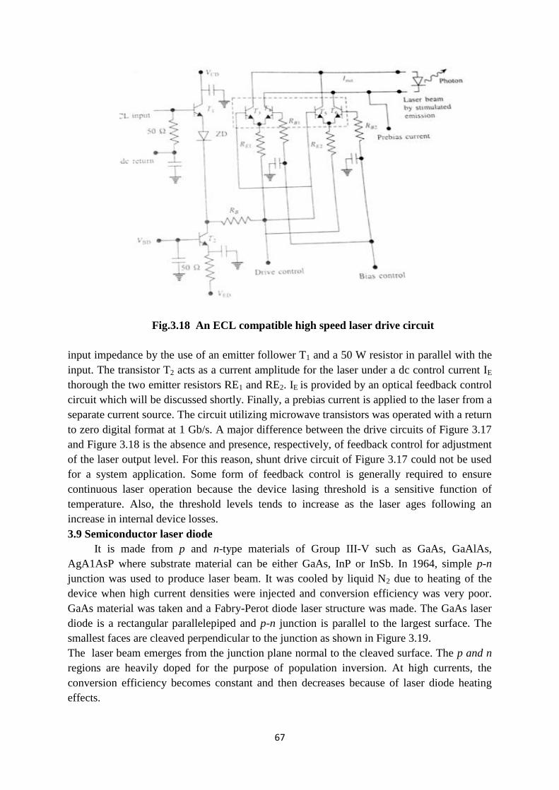
67
Fig.3.18 An ECL compatible high speed laser drive circuit
input impedance by the use of an emitter follower T1 and a 50 W resistor in parallel with the
input. The transistor T2 acts as a current amplitude for the laser under a dc control current IE
thorough the two emitter resistors RE1 and RE2. IE is provided by an optical feedback control
circuit which will be discussed shortly. Finally, a prebias current is applied to the laser from a
separate current source. The circuit utilizing microwave transistors was operated with a return
to zero digital format at 1 Gb/s. A major difference between the drive circuits of Figure 3.17
and Figure 3.18 is the absence and presence, respectively, of feedback control for adjustment
of the laser output level. For this reason, shunt drive circuit of Figure 3.17 could not be used
for a system application. Some form of feedback control is generally required to ensure
continuous laser operation because the device lasing threshold is a sensitive function of
temperature. Also, the threshold levels tends to increase as the laser ages following an
increase in internal device losses.
3.9 Semiconductor laser diode
It is made from p and n-type materials of Group III-V such as GaAs, GaAlAs,
AgA1AsP where substrate material can be either GaAs, InP or InSb. In 1964, simple p-n
junction was used to produce laser beam. It was cooled by liquid N2 due to heating of the
device when high current densities were injected and conversion efficiency was very poor.
GaAs material was taken and a Fabry-Perot diode laser structure was made. The GaAs laser
diode is a rectangular parallelepiped and p-n junction is parallel to the largest surface. The
smallest faces are cleaved perpendicular to the junction as shown in Figure 3.19.
The laser beam emerges from the junction plane normal to the cleaved surface. The p and n
regions are heavily doped for the purpose of population inversion. At high currents, the
conversion efficiency becomes constant and then decreases because of laser diode heating
effects.
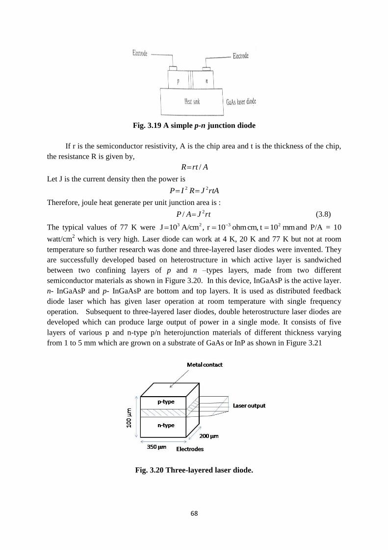
68
Fig. 3.19 A simple p-n junction diode
If r is the semiconductor resistivity, A is the chip area and t is the thickness of the chip,
the resistance R is given by,
ArtR /
Let J is the current density then the power is
rtAJRIP 22
Therefore, joule heat generate per unit junction area is :
rtJAP 2/ (3.8)
The typical values of 77 K were mm10tcm,ohm10r,A/cm10J 2323 and P/A = 10
watt/cm2 which is very high. Laser diode can work at 4 K, 20 K and 77 K but not at room
temperature so further research was done and three-layered laser diodes were invented. They
are successfully developed based on heterostructure in which active layer is sandwiched
between two confining layers of p and n –types layers, made from two different
semiconductor materials as shown in Figure 3.20. In this device, InGaAsP is the active layer.
n- InGaAsP and p- InGaAsP are bottom and top layers. It is used as distributed feedback
diode laser which has given laser operation at room temperature with single frequency
operation. Subsequent to three-layered laser diodes, double heterostructure laser diodes are
developed which can produce large output of power in a single mode. It consists of five
layers of various p and n-type p/n heterojunction materials of different thickness varying
from 1 to 5 mm which are grown on a substrate of GaAs or InP as shown in Figure 3.21
Fig. 3.20 Three-layered laser diode.
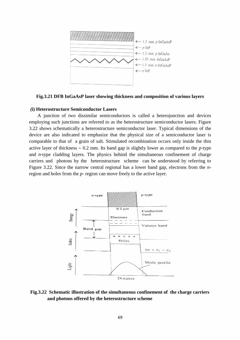
69
Fig.3.21 DFB InGaAsP laser showing thickness and composition of various layers
(i) Heterostructure Semiconductor Lasers
A junction of two dissimilar semiconductors is called a heterojunction and devices
employing such junctions are referred to as the heterostructure semiconductor lasers. Figure
3.22 shows schematically a heterostructure semiconductor laser. Typical dimensions of the
device are also indicated to emphasize that the physical size of a semiconductor laser is
comparable to that of a grain of salt. Stimulated recombination occurs only inside the thin
active layer of thickness 0.2 mm. Its band gap is slightly lower as compared to the p-type
and n-type cladding layers. The physics behind the simultaneous confinement of charge
carriers and photons by the heterostructure scheme can be understood by referring to
Figure 3.22. Since the narrow central regional has a lower band gap, electrons from the n-
region and holes from the p- region can move freely to the active layer.
Fig.3.22 Schematic illustration of the simultaneous confinement of the charge carriers
and photons offered by the heterostructure scheme
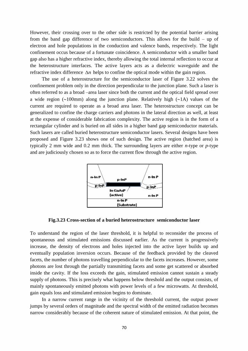
70
However, their crossing over to the other side is restricted by the potential barrier arising
from the band gap difference of two semiconductors. This allows for the build – up of
electron and hole populations in the conduction and valence bands, respectively. The light
confinement occus because of a fortunate coincidence. A semiconductor with a smaller band
gap also has a higher refractive index, thereby allowing the total internal reflection to occur at
the heterostructure interfaces. The active layers acts as a dielectric waveguide and the
refractive index difference n helps to confine the optical mode within the gain region.
The use of a heterostructure for the semiconductor laser of Figure 3.22 solves the
confinement problem only in the direction perpendicular to the junction plane. Such a laser is
often referred to as a broad –area laser since both the current and the optical field spread over
a wide region (100mm) along the junction plane. Relatively high (1A) values of the
current are required to operate as a broad area laser. The heterostructure concept can be
generalized to confine the charge carriers and photons in the lateral direction as well, at least
at the expense of considerable fabrication complexity. The active region is in the form of a
rectangular cylinder and is buried on all sides in a higher band gap semiconductor materials.
Such lasers are called buried heterostructure semiconductor lasers. Several designs have been
proposed and Figure 3.23 shows one of such design. The active region (hatched area) is
typically 2 mm wide and 0.2 mm thick. The surrounding layers are either n-type or p-type
and are judiciously chosen so as to force the current flow through the active region.
Fig.3.23 Cross-section of a buried heterostructure semiconductor laser
To understand the region of the laser threshold, it is helpful to reconsider the process of
spontaneous and stimulated emissions discussed earlier. As the current is progressively
increase, the density of electrons and holes injected into the active layer builds up and
eventually population inversion occurs. Because of the feedback provided by the cleaved
facets, the number of photons travelling perpendicular to the facets increases. However, some
photons are lost through the partially transmitting facets and some get scattered or absorbed
inside the cavity. If the loss exceeds the gain, stimulated emission cannot sustain a steady
supply of photons. This is precisely what happens below threshold and the output consists, of
mainly spontaneously emitted photons with power levels of a few microwatts. At threshold,
gain equals loss and stimulated emission begins to dominate.
In a narrow current range in the vicinity of the threshold current, the output power
jumps by several orders of magnitude and the spectral width of the emitted radiation becomes
narrow considerably because of the coherent nature of stimulated emission. At that point, the
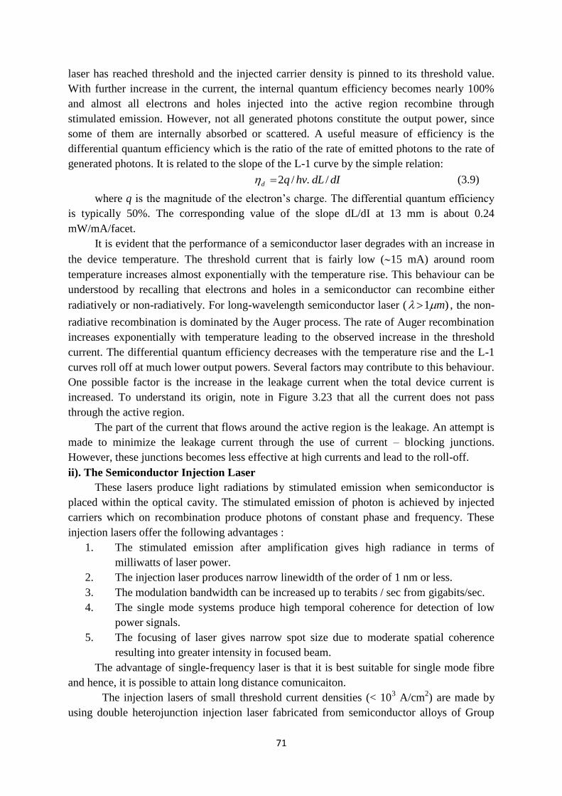
71
laser has reached threshold and the injected carrier density is pinned to its threshold value.
With further increase in the current, the internal quantum efficiency becomes nearly 100%
and almost all electrons and holes injected into the active region recombine through
stimulated emission. However, not all generated photons constitute the output power, since
some of them are internally absorbed or scattered. A useful measure of efficiency is the
differential quantum efficiency which is the ratio of the rate of emitted photons to the rate of
generated photons. It is related to the slope of the L-1 curve by the simple relation:
dIdLhvqd /./2 (3.9)
where q is the magnitude of the electron’s charge. The differential quantum efficiency
is typically 50%. The corresponding value of the slope dL/dI at 13 mm is about 0.24
mW/mA/facet.
It is evident that the performance of a semiconductor laser degrades with an increase in
the device temperature. The threshold current that is fairly low (15 mA) around room
temperature increases almost exponentially with the temperature rise. This behaviour can be
understood by recalling that electrons and holes in a semiconductor can recombine either
radiatively or non-radiatively. For long-wavelength semiconductor laser ( )1 m , the non-
radiative recombination is dominated by the Auger process. The rate of Auger recombination
increases exponentially with temperature leading to the observed increase in the threshold
current. The differential quantum efficiency decreases with the temperature rise and the L-1
curves roll off at much lower output powers. Several factors may contribute to this behaviour.
One possible factor is the increase in the leakage current when the total device current is
increased. To understand its origin, note in Figure 3.23 that all the current does not pass
through the active region.
The part of the current that flows around the active region is the leakage. An attempt is
made to minimize the leakage current through the use of current – blocking junctions.
However, these junctions becomes less effective at high currents and lead to the roll-off.
ii). The Semiconductor Injection Laser
These lasers produce light radiations by stimulated emission when semiconductor is
placed within the optical cavity. The stimulated emission of photon is achieved by injected
carriers which on recombination produce photons of constant phase and frequency. These
injection lasers offer the following advantages :
1. The stimulated emission after amplification gives high radiance in terms of
milliwatts of laser power.
2. The injection laser produces narrow linewidth of the order of 1 nm or less.
3. The modulation bandwidth can be increased up to terabits / sec from gigabits/sec.
4. The single mode systems produce high temporal coherence for detection of low
power signals.
5. The focusing of laser gives narrow spot size due to moderate spatial coherence
resulting into greater intensity in focused beam.
The advantage of single-frequency laser is that it is best suitable for single mode fibre
and hence, it is possible to attain long distance comunicaiton.
The injection lasers of small threshold current densities (< 103 A/cm
2) are made by
using double heterojunction injection laser fabricated from semiconductor alloys of Group
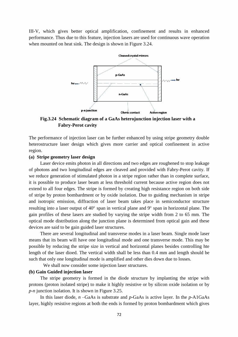
72
III-V, which gives better optical amplification, confinement and results in enhanced
performance. Thus due to this feature, injection lasers are used for continuous wave operation
when mounted on heat sink. The design is shown in Figure 3.24.
Fig.3.24 Schematic diagram of a GaAs heterojunction injection laser with a
Fabry-Perot cavity
The performance of injection laser can be further enhanced by using stripe geometry double
heterostructure laser design which gives more carrier and optical confinement in active
region.
(a) Stripe geometry laser design
Laser device emits photon in all directions and two edges are roughened to stop leakage
of photons and two longitudinal edges are cleaved and provided with Fabry-Perot cavity. If
we reduce generation of stimulated photon in a stripe region rather than in complete surface,
it is possible to produce laser beam at less threshold current because active region does not
extend to all four edges. The stripe is formed by creating high resistance region on both side
of stripe by proton bombardment or by oxide isolation. Due to guiding mechanism in stripe
and isotropic emission, diffraction of laser beam takes place in semiconductor structure
resulting into a laser output of 40 span in vertical plane and 9 span in horizontal plane. The
gain profiles of these lasers are studied by varying the stripe width from 2 to 65 mm. The
optical mode distribution along the junction plane is determined from optical gain and these
devices are said to be gain guided laser structures.
There are several longitudinal and transverse modes in a laser beam. Single mode laser
means that its beam will have one longitudinal mode and one transverse mode. This may be
possible by reducing the stripe size in vertical and horizontal planes besides controlling hte
length of the laser dioed. The vertical width shall be less than 0.4 mm and length should be
such that only one longitudinal mode is amplified and other dies down due to losses.
We shall now consider some injection laser structures.
(b) Gain Guided injection laser
The stripe geometry is formed in the diode structure by implanting the stripe with
protons (proton isolated stripe) to make it highly resistive or by silicon oxide isolation or by
p-n junction isolation. It is shown in Figure 3.25.
In this laser diode, n –GaAs is substrate and p-GaAs is active layer. In the p-A1GaAs
layer, highly resistive regions at both the ends is formed by proton bombardment which gives
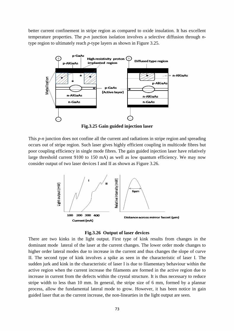
73
better current confinement in stripe region as compared to oxide insulation. It has excellent
temperature properties. The p-n junction isolation involves a selective diffusion through n-
type region to ultimately reach p-type layers as shown in Figure 3.25.
Fig.3.25 Gain guided injection laser
This p-n junction does not confine all the current and radiations in stripe region and spreading
occurs out of stripe region. Such laser gives highly efficient coupling in multicode fibres but
poor coupling efficiency in single mode fibres. The gain guided injection laser have relatively
large threshold current 9100 to 150 mA) as well as low quantum efficiency. We may now
consider output of two laser devices I and II as shown as Figure 3.26.
Fig.3.26 Output of laser devices
There are two kinks in the light output. First type of kink results from changes in the
dominant mode lateral of the laser at the current changes. The lower order mode changes to
higher order lateral modes due to increase in the current and thus changes the slope of curve
II. The second type of kink involves a spike as seen in the characteristic of laser I. The
sudden jurk and kink in the characteristic of laser I is due to filamentary behaviour within the
active region when the current increase the filaments are formed in the active region due to
increase in current from the defects within the crystal structure. It is thus necessary to reduce
stripe width to less than 10 mm. In general, the stripe size of 6 mm, formed by a plannar
process, allow the fundamental lateral mode to grow. However, it has been notice in gain
guided laser that as the current increase, the non-linearties in the light output are seen.
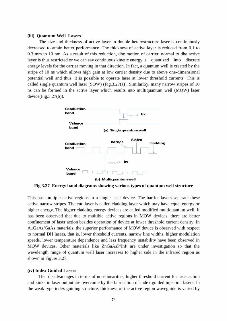
74
(iii) Quantum Well Lasers
The size and thickness of active layer in double heterostructure laser is continuously
decreased to attain better performance. The thickness of active layer is reduced from 0.1 to
0.3 mm to 10 nm. As a result of this reduction, dhe motion of carrier, normal to dhe active
layer is thus restricted or we can say continuous kinetic energy is quantized into discrete
energy levels for the carrier moving in that direction. In fact, a quantum well is created by the
stripe of 10 ns which allows high gain at low carrier density due to above one-dimensional
potential well and thus, it is possible to operate laser at lower threshold currents. This is
called single quantum well laser (SQW) (Fig.3.27(a)). Similarl6y, many narrow stripes of 10
ns can be formed in the active layer which results into multiquantum well (MQW) laser
device(Fig.3.27(b)).
Fig.3.27 Energy band diagrams showing various types of quantum well structure
This has multiple active regions in a single laser device. The barrier layers separate these
active narrow stripes. The end layer is called cladding layer which may have equal energy or
higher energy. The higher cladding energy devices are called modified multiquantum well. It
has been observed that due to multible active regions in MQW devices, there are better
confinement of laser action besides operation of device at lower threshold current density. In
A1GaAs/GaAs materials, the superior performance of MQW device is observed with respect
to normal DH lasers, that is, lower threshold currents, narrow line widths, higher modulation
speeds, lower temperature dependence and less frequency instability have been observed in
MQW devices. Other materials like ZnGaAsP/InP are under investigation so that the
wavelength range of quantum well laser increases to higher side in the infrared region as
shown in Figure 3.27.
(iv) Index Guided Lasers
The disadvantages in terms of non-linearities, higher threshold current for laser action
and kinks in laser output are overcome by the fabrication of index guided injection lasers. In
the weak type index guiding structure, thickness of the active region waveguide is varied by
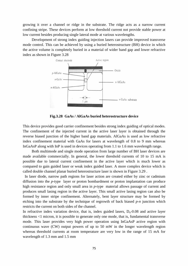
75
growing it over a channel or ridge in the substrate. The ridge acts as a narrow current
confining stripe. These devices perform at low threshold current not provide stable power at
low current besides producing single lateral mode at various wavelengths.
Development of strong index guiding injection lasers can provide improved transverse
mode control. This can be achieved by using a buried heterostructure (BH) device in which
the active volume is completely buried in a material of wider band gap and lower refractive
index as shown in Figure 3.28
Fig.3.28 GaAs / AlGaAs buried heterostructure device
This device provides good carrier confinement besides strong index guiding of optical modes.
The confinement of the injected current in the active laser layer is obtained through the
reverse biased junction of the higher band gap materials. AlGaAs is used as low refractive
index confinement material with GaAs for lasers at wavelength of 0.8 to 9 mm whereas
InGaAsP along with InP is used in devices operating from 1.1 to 1.6 mm wavelength range.
Both multimode and single mode operation from large number of BH laser devices are
made available commercially. In general, the lower threshold currents of 10 to 15 mA is
possible due to lateral current confinement in the active layer which is much lower as
compared to gain guided laser or weak index guided laser. A more complex device which is
called double channel planar buried heterostructure laser is shown in Figure 3.29 .
In laser diode, narrow path regions for laser action are created either by zinc or cadmium
diffusion into the p-type layer or proton bombardment or proton implantation can produce
high resistance region and only small area in p-type material allows passage of current and
produces small lasing region in the active layer. This small active lasing region can also be
formed by inner stripe confinement. Alternately, bent layer structure may be formed by
etching into the substrate by the technique of regrowth of back biased p-n junction which
restricts the current on both sides of the channel.
In refractive index variation device, that is, index guided lasers, Dn-0.08 and active layer
thickness <1 micron, it is possible to generate only one mode, that is, fundamental transverse
mode. This laser provides very high power operation using InGaAsP active region with
continuous wave (CW) output powers of up to 50 mW in the longer wavelength region
whereas threshold currents at room temperature are very low in the range of 15 mA for
wavelength of 1.3 mm and 1.5 mm
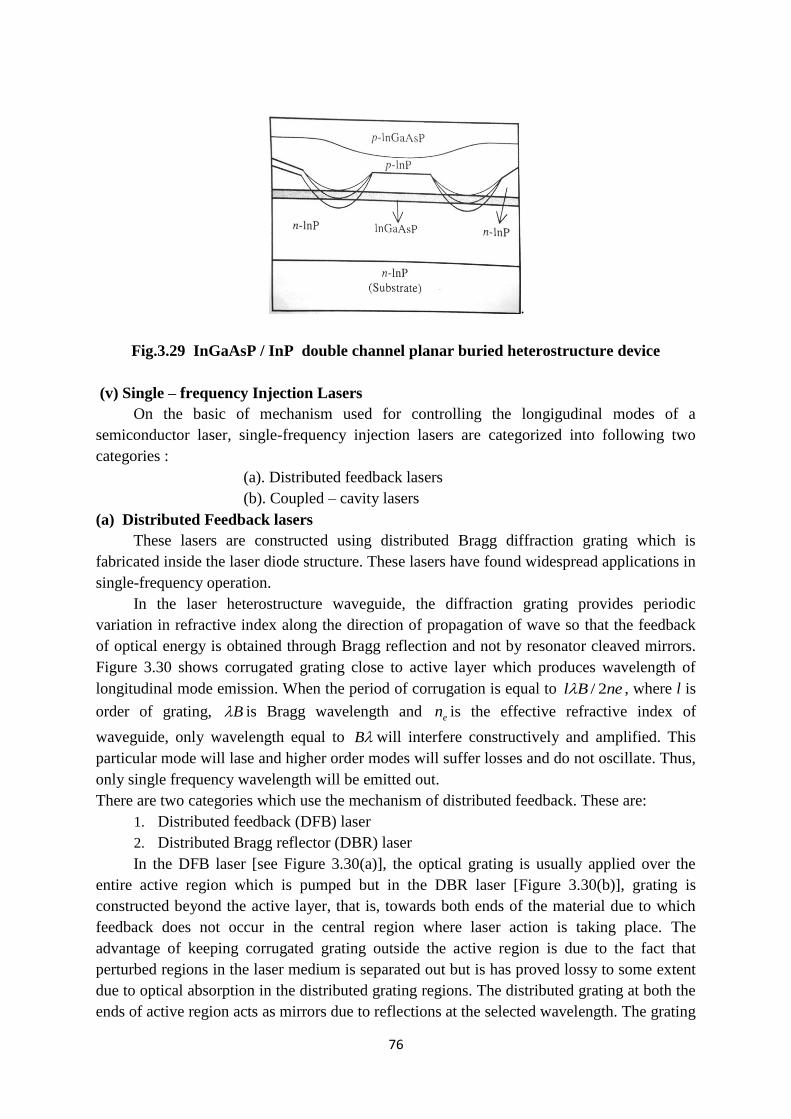
76
.
Fig.3.29 InGaAsP / InP double channel planar buried heterostructure device
(v) Single – frequency Injection Lasers
On the basic of mechanism used for controlling the longigudinal modes of a
semiconductor laser, single-frequency injection lasers are categorized into following two
categories :
(a). Distributed feedback lasers
(b). Coupled – cavity lasers
(a) Distributed Feedback lasers
These lasers are constructed using distributed Bragg diffraction grating which is
fabricated inside the laser diode structure. These lasers have found widespread applications in
single-frequency operation.
In the laser heterostructure waveguide, the diffraction grating provides periodic
variation in refractive index along the direction of propagation of wave so that the feedback
of optical energy is obtained through Bragg reflection and not by resonator cleaved mirrors.
Figure 3.30 shows corrugated grating close to active layer which produces wavelength of
longitudinal mode emission. When the period of corrugation is equal to neBl 2/ , where l is
order of grating, B is Bragg wavelength and en is the effective refractive index of
waveguide, only wavelength equal to B will interfere constructively and amplified. This
particular mode will lase and higher order modes will suffer losses and do not oscillate. Thus,
only single frequency wavelength will be emitted out.
There are two categories which use the mechanism of distributed feedback. These are:
1. Distributed feedback (DFB) laser
2. Distributed Bragg reflector (DBR) laser
In the DFB laser [see Figure 3.30(a)], the optical grating is usually applied over the
entire active region which is pumped but in the DBR laser [Figure 3.30(b)], grating is
constructed beyond the active layer, that is, towards both ends of the material due to which
feedback does not occur in the central region where laser action is taking place. The
advantage of keeping corrugated grating outside the active region is due to the fact that
perturbed regions in the laser medium is separated out but is has proved lossy to some extent
due to optical absorption in the distributed grating regions. The distributed grating at both the
ends of active region acts as mirrors due to reflections at the selected wavelength. The grating
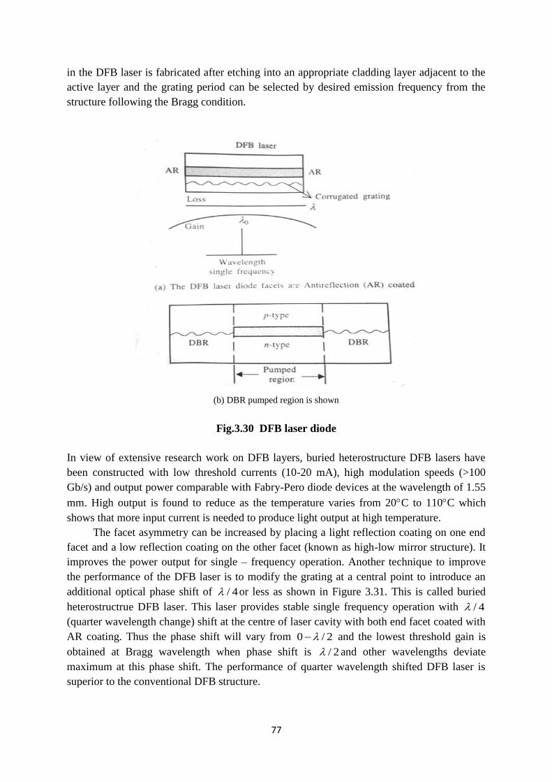
77
in the DFB laser is fabricated after etching into an appropriate cladding layer adjacent to the
active layer and the grating period can be selected by desired emission frequency from the
structure following the Bragg condition.
(b) DBR pumped region is shown
Fig.3.30 DFB laser diode
In view of extensive research work on DFB layers, buried heterostructure DFB lasers have
been constructed with low threshold currents (10-20 mA), high modulation speeds (>100
Gb/s) and output power comparable with Fabry-Pero diode devices at the wavelength of 1.55
mm. High output is found to reduce as the temperature varies from 20C to 110C which
shows that more input current is needed to produce light output at high temperature.
The facet asymmetry can be increased by placing a light reflection coating on one end
facet and a low reflection coating on the other facet (known as high-low mirror structure). It
improves the power output for single – frequency operation. Another technique to improve
the performance of the DFB laser is to modify the grating at a central point to introduce an
additional optical phase shift of 4/ or less as shown in Figure 3.31. This is called buried
heterostructrue DFB laser. This laser provides stable single frequency operation with 4/
(quarter wavelength change) shift at the centre of laser cavity with both end facet coated with
AR coating. Thus the phase shift will vary from 2/0 and the lowest threshold gain is
obtained at Bragg wavelength when phase shift is 2/ and other wavelengths deviate
maximum at this phase shift. The performance of quarter wavelength shifted DFB laser is
superior to the conventional DFB structure.
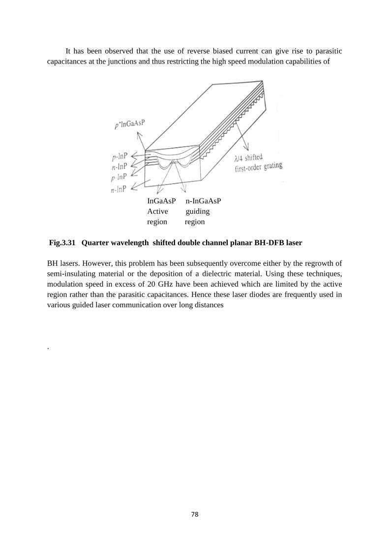
78
It has been observed that the use of reverse biased current can give rise to parasitic
capacitances at the junctions and thus restricting the high speed modulation capabilities of
InGaAsP n-InGaAsP
Active guiding
region region
Fig.3.31 Quarter wavelength shifted double channel planar BH-DFB laser
BH lasers. However, this problem has been subsequently overcome either by the regrowth of
semi-insulating material or the deposition of a dielectric material. Using these techniques,
modulation speed in excess of 20 GHz have been achieved which are limited by the active
region rather than the parasitic capacitances. Hence these laser diodes are frequently used in
various guided laser communication over long distances
.
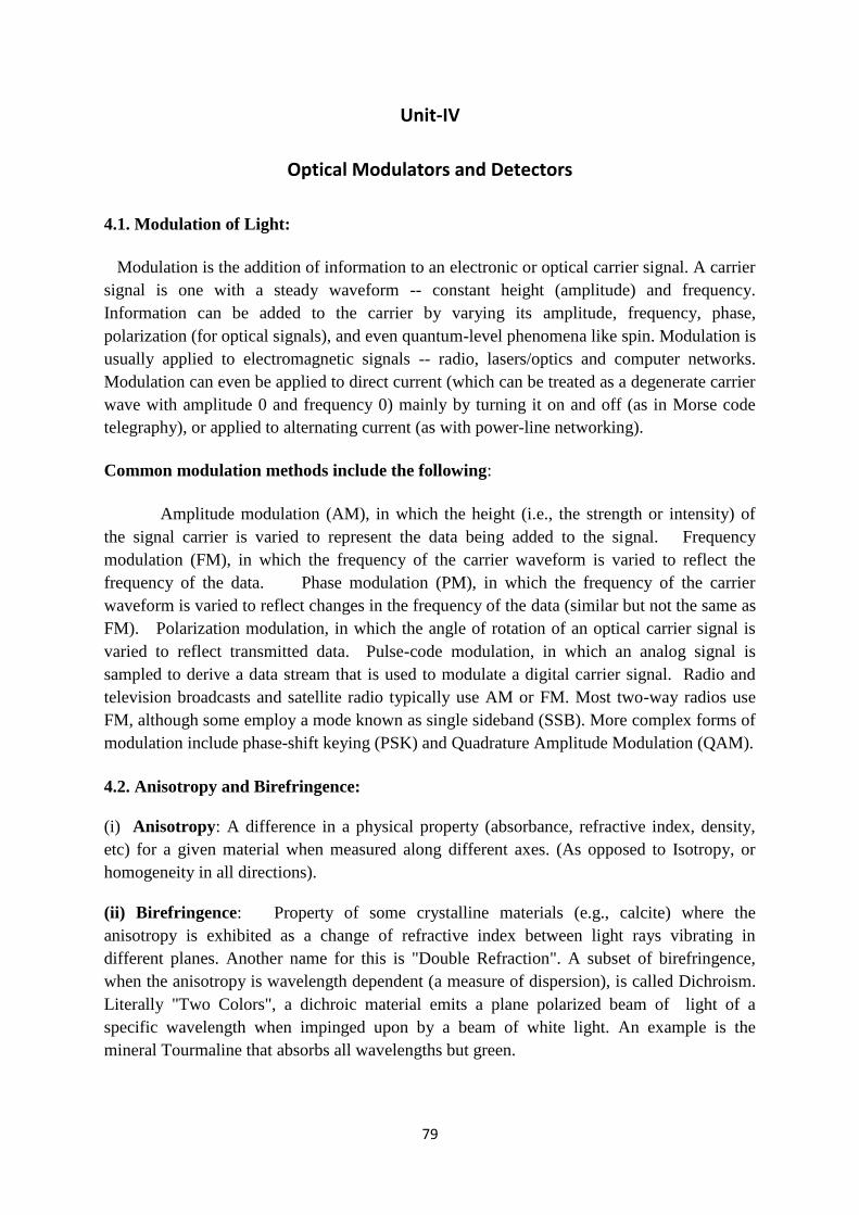
79
Unit-IV
Optical Modulators and Detectors
4.1. Modulation of Light:
Modulation is the addition of information to an electronic or optical carrier signal. A carrier
signal is one with a steady waveform -- constant height (amplitude) and frequency.
Information can be added to the carrier by varying its amplitude, frequency, phase,
polarization (for optical signals), and even quantum-level phenomena like spin. Modulation is
usually applied to electromagnetic signals -- radio, lasers/optics and computer networks.
Modulation can even be applied to direct current (which can be treated as a degenerate carrier
wave with amplitude 0 and frequency 0) mainly by turning it on and off (as in Morse code
telegraphy), or applied to alternating current (as with power-line networking).
Common modulation methods include the following:
Amplitude modulation (AM), in which the height (i.e., the strength or intensity) of
the signal carrier is varied to represent the data being added to the signal. Frequency
modulation (FM), in which the frequency of the carrier waveform is varied to reflect the
frequency of the data. Phase modulation (PM), in which the frequency of the carrier
waveform is varied to reflect changes in the frequency of the data (similar but not the same as
FM). Polarization modulation, in which the angle of rotation of an optical carrier signal is
varied to reflect transmitted data. Pulse-code modulation, in which an analog signal is
sampled to derive a data stream that is used to modulate a digital carrier signal. Radio and
television broadcasts and satellite radio typically use AM or FM. Most two-way radios use
FM, although some employ a mode known as single sideband (SSB). More complex forms of
modulation include phase-shift keying (PSK) and Quadrature Amplitude Modulation (QAM).
4.2. Anisotropy and Birefringence:
(i) Anisotropy: A difference in a physical property (absorbance, refractive index, density,
etc) for a given material when measured along different axes. (As opposed to Isotropy, or
homogeneity in all directions).
(ii) Birefringence: Property of some crystalline materials (e.g., calcite) where the
anisotropy is exhibited as a change of refractive index between light rays vibrating in
different planes. Another name for this is "Double Refraction". A subset of birefringence,
when the anisotropy is wavelength dependent (a measure of dispersion), is called Dichroism.
Literally "Two Colors", a dichroic material emits a plane polarized beam of light of a
specific wavelength when impinged upon by a beam of white light. An example is the
mineral Tourmaline that absorbs all wavelengths but green.
80
(iii) Birefringence number( ∆n): The numerical difference between the two refractive
indices of a birefringent substance. For example Calcite has a Refractive index (o-ray) =
1.658 and RI (e-ray) = 1.486, so the birefringence number = 0.172. Birefringence numbers
are diagnostic tools for identifying unknown substances.
Fig.4.1 Birefringent crystal
A: When a beam of non-polarized light passes into a crystal of calcite the vibrational plane
determines its velocity. Since refraction is a function of velocity, a beam of light will be
decomposed into two beams that refract at different angles (Fig.4.1(A)). One plane of
vibration will realize a higher refractive index and refract according to Snell's law. This is
called the "Ordinary-Ray". Another beam, vibrating at right angles to the O-Ray, will realize
an lower refractive index and bend at a lower angle. This beam is called the "Extraordinary-
Ray", or E-Ray. Thus, two spatially separated rays will exit the birefringent object. The rays
will be Plane Polarized, and will be vibrating orthogonal to each other. In addition, the slow
ray will lag in phase relative to the fast ray. When they emerge from the birefringent crystal,
they may interact via wave interference which results in the production of Interference Colors
(depending on the optical path of the material). The colors directly relate to the wave
Retardation. Below are refractive indices of the O- and E-rays of common birefringent
materials.
81
B: Creating a beam of plane polarized light- The Nicol Prism. The first device used to
produce a beam of polarized light was invented by William Nicol (1770–1851). It consists of
a piece of calcite, rhombohedral in shape, and cut at 68° (a, above). The crystal is then
bisected, one half inverted and glued back onto the first half. Canada Balsam (n=1.555) was
used originally to glue the two halves together. When non-polarized light impinges on the
crystal, the resulting slow, or O-Ray bends at an angle that results in total reflection at the
interface between the two halves. The faster, less refracted E-ray passes through the interface
and exits the opposite end of the crystal as a beam of plane polarized light. Modern polarizers
are made of iodine crystals embedded in a plastic (PVA) sheet ("H-Sheet"). When the sheet is
stretched, the crystals align. This Polaroid Filter produces plane polarized light in a manner
similar to the Nicol prism. Light that vibrates perpendicular to the crystal orientation pass
through the sheet. Light that vibrates parallel to the crystals interacts with the atomic
structure of the crystals and is absorbed(Fig.4.1(b)).
(iv) Common birefringent materials: The best-characterized birefringent materials are
crystals. Due to their specific crystal structures their refractive indices are well defined.
Depending on the symmetry of a crystal structure, crystals in that group may be forced to be
isotropic (not birefringent), to have uniaxial symmetry, or neither in which case it is a biaxial
crystal.
Many plastics are birefringent, because their molecules are 'frozen' in a stretched
conformation when the plastic is molded or extruded. For example, ordinary cellophane is
birefringent.
Polarizers are routinely used to detect stress in plastics such as polystyrene and
polycarbonate.
Cotton fiber is birefringent because of high levels of cellulosic material in the fiber's
secondary cell wall.
Polarized light microscopy is commonly used in biological tissue, as many biological
materials are birefringent. Collagen, found in cartilage, tendon, bone, corneas, and several
other areas in the body, is birefringent and commonly studied with polarized light
microscopy. Some proteins are also birefringent, exhibiting form birefringence.
Inevitable manufacturing imperfections in optical fiber leads to birefringence which is one
cause of pulse broadening in fiber-optic communications. Such imperfections can be
geometrical (lack of circular symmetry), due to stress applied to the optical fiber, and/or due
to bending of the fiber. Birefringence is intentionally introduced (for instance, by making the
cross-section elliptical) in order to produce polarization-maintaining optical fibers.
In addition to anisotropy in the electric polarizability (electric susceptibility), anisotropy in
the magnetic polarizability (magnetic permeability) can also cause birefringence. However at
optical frequencies, values of magnetic permeability for natural materials are not measurably
different from µ0 so this is not a source of optical birefringence in practice.
(v) Applications: Birefringence is used in many optical devices. Liquid crystal displays, the
most common sort of flat panel display, cause their pixels to become lighter or darker through
rotation of the polarization (circular birefringence) of linearly polarized light as viewed
82
through a sheet polarizer at the screen's surface. Similarly, light modulators modulate the
intensity of light through electrically induced birefringence of polarized light followed by a
polarizer. The Lyot filter is a specialized narrowband spectral filter employing the
wavelength dependence of birefringence. Wave plates are thin birefringent sheets widely
used in certain optical equipment for modifying the polarization state of light passing through
it.
Birefringence also plays an important role in second harmonic generation and other
nonlinear optical components, as the crystals used for this purpose are almost always
birefringent. By adjusting the angle of incidence, the effective refractive index of the
extraordinary ray can be tuned in order to achieve phase matching which is required for
efficient operation of these devices.
Medicine: Birefringence is utilized in medical diagnostics. One powerful accessory used
with optical microscopes is a pair of crossed polarizing filters. Light from the source is
polarized in the X direction after passing through the first polarizer, but above the specimen
is a polarizer (a so-called analyzer) oriented in the Y direction. Therefore, no light from the
source will be accepted by the analyzer, and the field will appear dark. However areas of the
sample possessing birefringence will generally couple some of the X polarized light into the
Y polarization; these areas will then appear bright against the dark background.
Modifications to this basic principle can differentiate between positive and negative
birefringence. Urate crystals, with the crystals with their long axis seen as horizontal in this
view being parallel to that of a red compensator filter. These appear as yellow, and are
thereby of negative birefringence.
In ophthalmology, binocular retinal birefringence screening of the Henle fibers provides a
reliable detection of strabismus and possibly also of anisometropic amblyopia. Furthermore,
scanning laser polarimetry utilises the birefringence of the optic nerve fibre layer to indirectly
quantify its thickness, which is of use in the assessment and monitoring of glaucoma.
Birefringence characteristics in sperm heads allow for the selection of spermatozoa for
intracytoplasmic sperm injection. Likewise, zona imaging uses birefringence on oocytes to
select the ones with highest chances of successful pregnancy. Birefringence of particles
biopsied from pulmonary nodules indicates silicosis. Dermatologists use dermatascopes to
view pigmented lesions and nevi. Dermatascopes use cross-polarized light, allowing the user
to view chrystaline structures corresponding to dermal collagen in the skin. These structures
may appear as shiny white lines or rosette shapes, and are only visible under polarized
dermoscopy.
Stress induced birefringence:
Isotropic solids do not exhibit birefringence. However, when they are under mechanical
stress, birefringence results. The stress can be applied externally or is "frozen in" after a
birefringent plastic ware is cooled after it is manufactured using injection molding. When
such a sample is placed between two crossed polarizers, colour patterns can be observed,
because polarization of a light ray is rotated after passing through a birefingent material and
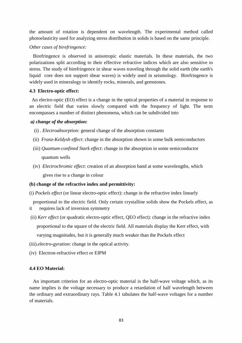
83
the amount of rotation is dependent on wavelength. The experimental method called
photoelasticity used for analyzing stress distribution in solids is based on the same principle.
Other cases of birefringence:
Birefringence is observed in anisotropic elastic materials. In these materials, the two
polarizations split according to their effective refractive indices which are also sensitive to
stress. The study of birefringence in shear waves traveling through the solid earth (the earth's
liquid core does not support shear waves) is widely used in seismology. Birefringence is
widely used in mineralogy to identify rocks, minerals, and gemstones.
4.3 Electro-optic effect:
An electro-optic (EO) effect is a change in the optical properties of a material in response to
an electric field that varies slowly compared with the frequency of light. The term
encompasses a number of distinct phenomena, which can be subdivided into
a) change of the absorption:
(i) . Electroabsorption: general change of the absorption constants
(ii) Franz-Keldysh effect: change in the absorption shown in some bulk semiconductors
(iii) Quantum-confined Stark effect: change in the absorption in some semiconductor
quantum wells
(iv) Electrochromic effect: creation of an absorption band at some wavelengths, which
gives rise to a change in colour
(b) change of the refractive index and permittivity:
(i) Pockels effect (or linear electro-optic effect): change in the refractive index linearly
proportional to the electric field. Only certain crystalline solids show the Pockels effect, as
it requires lack of inversion symmetry
(ii) Kerr effect (or quadratic electro-optic effect, QEO effect): change in the refractive index
proportional to the square of the electric field. All materials display the Kerr effect, with
varying magnitudes, but it is generally much weaker than the Pockels effect
(iii).electro-gyration: change in the optical activity.
(iv) Electron-refractive effect or EIPM
4.4 EO Material:
An important criterion for an electro-optic material is the half-wave voltage which, as its
name implies is the voltage necessary to produce a retardation of half wavelength between
the ordinary and extraordinary rays. Table 4.1 tabulates the half-wave voltages for a number
of materials.
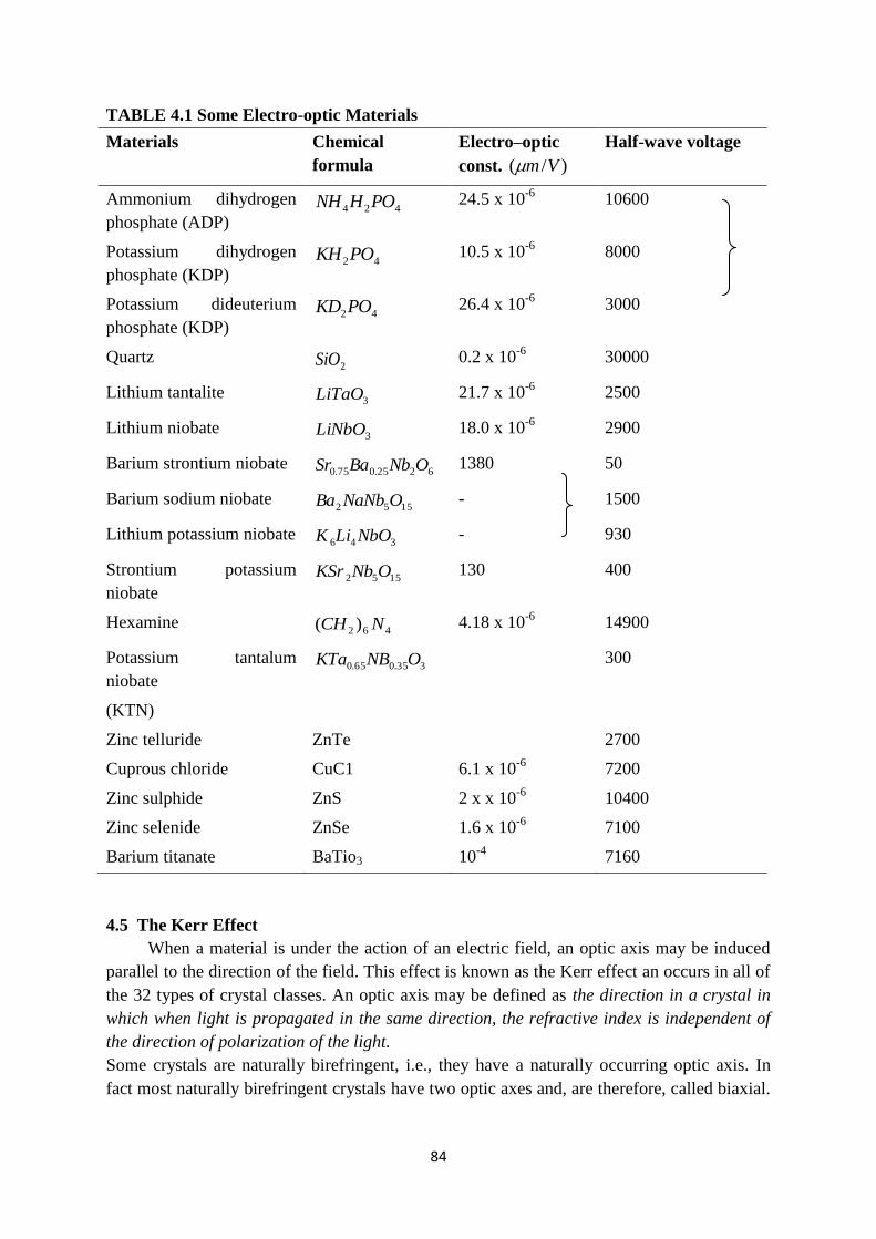
84
TABLE 4.1 Some Electro-optic Materials
Materials Chemical
formula
Electro–optic
const. )/( Vm
Half-wave voltage
Ammonium dihydrogen
phosphate (ADP) 424 POHNH 24.5 x 10
-6 10600
Potassium dihydrogen
phosphate (KDP) 42POKH 10.5 x 10
-6 8000
Potassium dideuterium
phosphate (KDP) 42POKD 26.4 x 10
-6 3000
Quartz 2SiO 0.2 x 10
-6 30000
Lithium tantalite 3LiTaO 21.7 x 10
-6 2500
Lithium niobate 3LiNbO 18.0 x 10
-6 2900
Barium strontium niobate 6225.075.0 ONbBaSr 1380 50
Barium sodium niobate 1552 ONaNbBa - 1500
Lithium potassium niobate 346 NbOLiK - 930
Strontium potassium
niobate 1552 ONbKSr 130 400
Hexamine 462 )( NCH 4.18 x 10
-6 14900
Potassium tantalum
niobate 335.065.0 ONBKTa 300
(KTN)
Zinc telluride ZnTe 2700
Cuprous chloride CuC1 6.1 x 10⁻⁶
7200
Zinc sulphide ZnS 2 x x 10-6
10400
Zinc selenide ZnSe 1.6 x 10⁻⁶
7100
Barium titanate BaTio3 10-4
7160
4.5 The Kerr Effect
When a material is under the action of an electric field, an optic axis may be induced
parallel to the direction of the field. This effect is known as the Kerr effect an occurs in all of
the 32 types of crystal classes. An optic axis may be defined as the direction in a crystal in
which when light is propagated in the same direction, the refractive index is independent of
the direction of polarization of the light.
Some crystals are naturally birefringent, i.e., they have a naturally occurring optic axis. In
fact most naturally birefringent crystals have two optic axes and, are therefore, called biaxial.
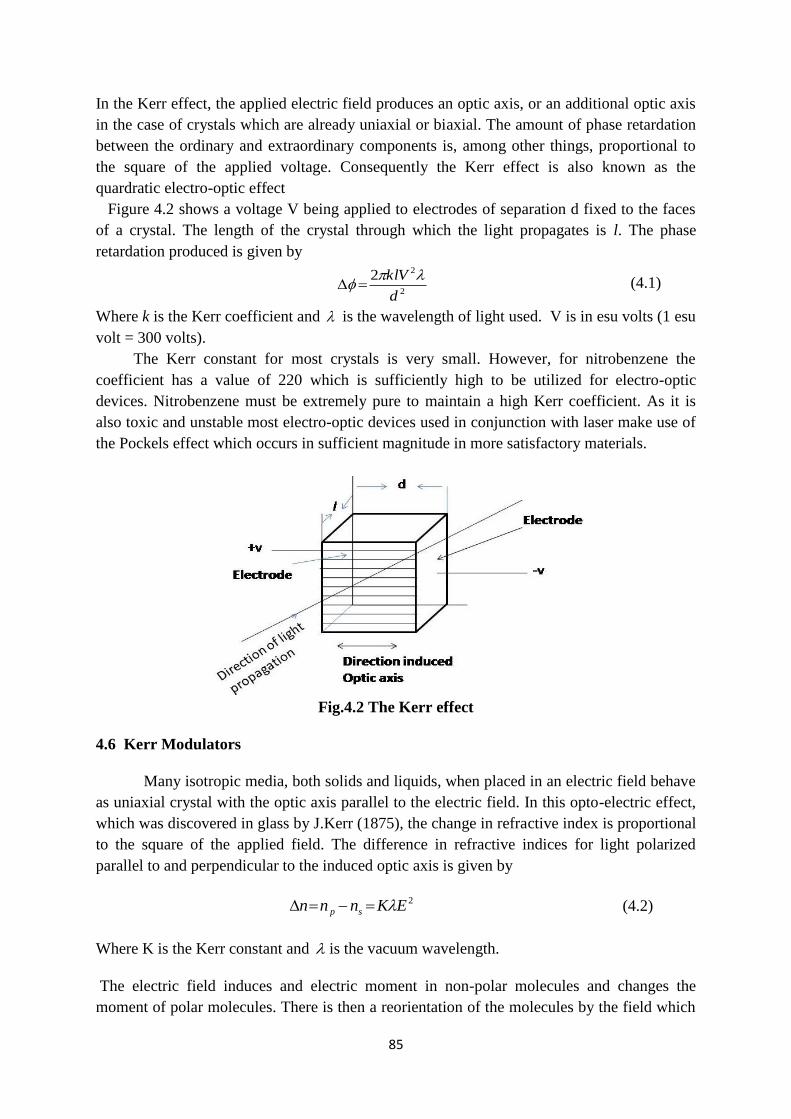
85
In the Kerr effect, the applied electric field produces an optic axis, or an additional optic axis
in the case of crystals which are already uniaxial or biaxial. The amount of phase retardation
between the ordinary and extraordinary components is, among other things, proportional to
the square of the applied voltage. Consequently the Kerr effect is also known as the
quardratic electro-optic effect
Figure 4.2 shows a voltage V being applied to electrodes of separation d fixed to the faces
of a crystal. The length of the crystal through which the light propagates is l. The phase
retardation produced is given by
2
22
d
klV (4.1)
Where k is the Kerr coefficient and is the wavelength of light used. V is in esu volts (1 esu
volt = 300 volts).
The Kerr constant for most crystals is very small. However, for nitrobenzene the
coefficient has a value of 220 which is sufficiently high to be utilized for electro-optic
devices. Nitrobenzene must be extremely pure to maintain a high Kerr coefficient. As it is
also toxic and unstable most electro-optic devices used in conjunction with laser make use of
the Pockels effect which occurs in sufficient magnitude in more satisfactory materials.
Fig.4.2 The Kerr effect
4.6 Kerr Modulators
Many isotropic media, both solids and liquids, when placed in an electric field behave
as uniaxial crystal with the optic axis parallel to the electric field. In this opto-electric effect,
which was discovered in glass by J.Kerr (1875), the change in refractive index is proportional
to the square of the applied field. The difference in refractive indices for light polarized
parallel to and perpendicular to the induced optic axis is given by
2EKnnn sp (4.2)
Where K is the Kerr constant and is the vacuum wavelength.
The electric field induces and electric moment in non-polar molecules and changes the
moment of polar molecules. There is then a reorientation of the molecules by the field which
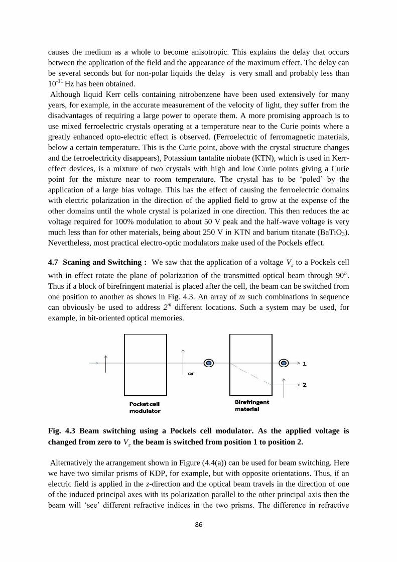
86
causes the medium as a whole to become anisotropic. This explains the delay that occurs
between the application of the field and the appearance of the maximum effect. The delay can
be several seconds but for non-polar liquids the delay is very small and probably less than
10-11
Hz has been obtained.
Although liquid Kerr cells containing nitrobenzene have been used extensively for many
years, for example, in the accurate measurement of the velocity of light, they suffer from the
disadvantages of requiring a large power to operate them. A more promising approach is to
use mixed ferroelectric crystals operating at a temperature near to the Curie points where a
greatly enhanced opto-electric effect is observed. (Ferroelectric of ferromagnetic materials,
below a certain temperature. This is the Curie point, above with the crystal structure changes
and the ferroelectricity disappears), Potassium tantalite niobate (KTN), which is used in Kerr-
effect devices, is a mixture of two crystals with high and low Curie points giving a Curie
point for the mixture near to room temperature. The crystal has to be ‘poled’ by the
application of a large bias voltage. This has the effect of causing the ferroelectric domains
with electric polarization in the direction of the applied field to grow at the expense of the
other domains until the whole crystal is polarized in one direction. This then reduces the ac
voltage required for 100% modulation to about 50 V peak and the half-wave voltage is very
much less than for other materials, being about 250 V in KTN and barium titanate (BaTiO3).
Nevertheless, most practical electro-optic modulators make used of the Pockels effect.
4.7 Scaning and Switching : We saw that the application of a voltage V to a Pockels cell
with in effect rotate the plane of polarization of the transmitted optical beam through 90.
Thus if a block of birefringent material is placed after the cell, the beam can be switched from
one position to another as shows in Fig. 4.3. An array of m such combinations in sequence
can obviously be used to address 2m different locations. Such a system may be used, for
example, in bit-oriented optical memories.
Fig. 4.3 Beam switching using a Pockels cell modulator. As the applied voltage is
changed from zero to V the beam is switched from position 1 to position 2.
Alternatively the arrangement shown in Figure (4.4(a)) can be used for beam switching. Here
we have two similar prisms of KDP, for example, but with opposite orientations. Thus, if an
electric field is applied in the z-direction and the optical beam travels in the direction of one
of the induced principal axes with its polarization parallel to the other principal axis then the
beam will ‘see’ different refractive indices in the two prisms. The difference in refractive
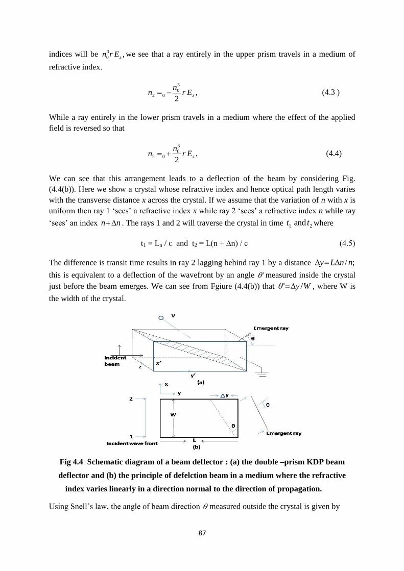
87
indices will be ,3
0 zErn we see that a ray entirely in the upper prism travels in a medium of
refractive index.
,2
3
002 zEr
nn (4.3 )
While a ray entirely in the lower prism travels in a medium where the effect of the applied
field is reversed so that
,2
3
002 zEr
nn (4.4)
We can see that this arrangement leads to a deflection of the beam by considering Fig.
(4.4(b)). Here we show a crystal whose refractive index and hence optical path length varies
with the transverse distance x across the crystal. If we assume that the variation of n with x is
uniform then ray 1 ‘sees’ a refractive index x while ray 2 ‘sees’ a refractive index n while ray
‘sees’ an index nn . The rays 1 and 2 will traverse the crystal in time 21 and tt where
t1 = Ln / c and t2 = L(n + ∆n) / c (4.5)
The difference is transit time results in ray 2 lagging behind ray 1 by a distance ;/ nnLy
this is equivalent to a deflection of the wavefront by an angle ' measured inside the crystal
just before the beam emerges. We can see from Fgiure (4.4(b)) that Wy /' , where W is
the width of the crystal.
Fig 4.4 Schematic diagram of a beam deflector : (a) the double –prism KDP beam
deflector and (b) the principle of defelction beam in a medium where the refractive
index varies linearly in a direction normal to the direction of propagation.
Using Snell’s law, the angle of beam direction measured outside the crystal is given by
88
(assuming issmall)
) 4.3 ( Figure from ,'Where,W
y
W
ynn
(Or) y
L
n
nas
W
nL
,
Thus, using the arrangement shown in Figure (4.4(a)) the deflection is given by
,)/( 3
0 zErnWL
(4.6 )
Light beams can also be deflected by means of diffraction gratings which are electro-
optically induced in a crystal by evaporating a periodic metallic grating electrode onto the
crystal. A voltage applied to this electrode induces a periodic variation in the refractive index
thereby creating an efficient phase diffraction grating. This technique is especially usefull in
the integrated optical devices. Beam deflectors and scanners are used in laser displays,
printers and scribers, for optical data storage systems and in optical character recognition.
4.8 Magneto – Optic (MO) devices :
The presence of magnetic field may also effect the optical properties of some
substances thereby giving rise to a number of useful devices. In general, however, as electric
fields are easier to generate than magnetic fields, electro-optic devices are usually preferred
to magneto-optic devices.
(i) Faraday Effect
This is the simplest magneto-optic effect and the only one of real interest for optical
modulators; it concerns the change in refractive index of a material subjected to a steady
magnetic field. Faraday (1845) found that when a beam of plane polarized light passes
through a substance subjected to a magnetic field, its plane of polarization is observed to
rotate by an amount proportional to the magnetic field components parallel to the direction of
propagation. This is very similar to optical activity which results from certain materials
having different refractive indices 1and nnr for light and left circularly polarized light. There
is one important difference in the two effects. In the Faraday effect the sense of rotation of
the plane of polarization is independent of the direction of propagation. This is in contrast to
optical activity where the sense of rotation is related to the direction of propagation. Thus, in
the case under discussion, the rotation can be doubled by reflecting the light back through the
Faraday effect device.
The rotation of the plane of polarization is given by
VBL (4.6)
89
Where V is the Verdet constant, B is the magnetic flux parallel to the direction of propagation
and L is the path length in the material. The Faraday effect is small and wavelength
dependent: the rotation for dense flint glass is nm3.589at6.1 11 Tmm . We can
also express in terms of the refractive indices 1and nnr i.e.,
Lnnr )-(
21
(4.7)
A Faraday rotator used in conjunction with a pair of polarizers acts as an optical isolator
which allows a light beam to travel through it in one direction but not in the opposite one. It
may therefore be used in laser amplifying chains to eliminate reflected, backward travelling
waves, which are potentially damaging. The construction of a typical isolator is shown in
Fig.4.5. Light passing from left to right is polarized in the vertical plane by polarizer P1.
The Faraday rotator is adjusted to produce a rotation of 45 in the clockwise sense. The
second Polarizer P2 is set at 45 to P1 so that it will transmit light emerging from the rotator.
However, a beam entering from the right will be plane polarized at 45 to the vertical by P2
and then have its plane rotated by 45 in the clockwise sense by the rotator. It will therefore
be incident on P1 with its plane of polarization at right angles to the plane of transmission and
be eliminated. The device thus isolates the components on its left from light incident from the
light.
Fig. 4.5: Optical isolator based on the Faraday effect. The reflected ray is shown
displaced for clarity.
One potential application of magneto-optics currently receiving attention is large
capacity computer memories. Such memories must be capable of storing very large amounts
of information in a relatively small area and permit very rapid readout and, preferably,
random access. The usual magnetic memories have a number of limitations of size and
reading speed. Optical techniques can overcome both these constraints.
The magneto-optic memories developed so far are read via the Faraday effect or the
magnetic Kerr effect, which relates to the rotation of a beam of plane polarized light reflected
from the surface of a material subjected to a magnetic field. In either case a magnetized ferro-
or ferromagnetic material rotates the plane of polarization of laser light incident on it.
90
4.9 Acousto – Optic (AO) effect
The acousto – optic effect is the change in the refractive index of a medium caused by
the mechanical strains accompanying the passage of an acoustic (strain) wave through the
medium. The strain and hence the refractive index varies periodically with a wavelength
equal to that of the acoustic wave. The refractive index changes are caused by the
photoelastic effect which occurs in all materials on the application of a mechanical stress. It
can be shown that the change in refractive index is proportional to the square root of the total
acoustic power.
In general, the relationships between changes of refractive index and mechanical
strain, and between the strain and stress are rather complicated. However, for simplicity we
can consider the case of a monochromatic light wave, wavelength , incident upon a
medium in which an acoustic wave has produced sinusoidal variations of wavelength in the
refractive index. The situation is shown in Figure 4.5 where the solid horizontal lines
represent acoustic wave peaks (pressure maxima) and the dashed horizontal lines represent
acoustic wave peaks (pressure maxima). As the light enters the medium, the portions of the
wavefront near to a pressure peak will encounter a higher refractive index and, therefore,
advance with a lower velocity than those portions of the wavefront which encounter pressure
minima. The wavefront in the midum therefore soon acquires the wavy appearance shown by
the dashed curve in Fig. 4.6. The acoustic wave velocity is very much less than the light wave
velocity, so we may ignore it and consider the variation in refractice index to be stationary in
the medium.As elements of the light wave propagate in a direction normal to the local
wavefront, almost all the wave elements will suffer a change in direction leading to a re-
distribution of the light flux, which tends to concentrate near regions of compression. In
effect, the acoustic wave sets up a diffraction grating within the medium so that the optical
energy is diffracted out of the incident beam into the various orders. There are two main
cases of interest, namely (a) the Raman-Nath regime and (b) the Bragg regime.
Fig. 4.6 Schematic illustration of acousto – optic modulation. The acoustic waves
change the refractive index of the medium in a periodic way so that the plane optical
wavefronts take on the ‘wavy’ appearance shown (very much exaggerated) as they
propagate through the medium.
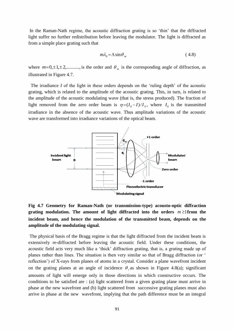
91
In the Raman-Nath regime, the acoustic diffraction grating is so ‘thin’ that the diffracted
light suffer no further redistribution before leaving the modulator. The light is diffracted as
from a simple place grating such that
mm sin0 ( 4.8)
where ..,,.........2,1,0 m is the order and m is the corresponding angle of diffraction, as
illustrated in Figure 4.7.
The irradiance I of the light in these orders depends on the ‘ruling depth’ of the acoustic
grating, which is related to the amplitude of the acoustic grating. This, in turn, is related to
the amplitude of the acoustic modulating wave (that is, the stress produced). The fraction of
light removed from the zero order beam is 00 /)( III , where 0I is the transmitted
irradiance in the absence of the acoustic wave. Thus amplitude variations of the acoustic
wave are transformed into irradiance variations of the optical beam.
Fig 4.7 Geometry for Raman-Nath (or transmission-type) acousto-optic diffraction
grating modulation. The amount of light diffracted into the orders 1m from the
incident beam, and hence the modulation of the transmitted beam, depends on the
amplitude of the modulating signal.
The physical basis of the Bragg regime is that the light diffracted from the incident beam is
extensively re-diffracted before leaving the acoustic field. Under these conditions, the
acoustic field acts very much like a ‘thick’ diffraction grating, that is, a grating made up of
planes rather than lines. The situation is then very similar so that of Bragg diffraction (or ‘
reflection’) of X-rays from planes of atoms in a crystal. Consider a plane wavefront incident
on the grating planes at an angle of incidence i as shown in Figure 4.8(a); significant
amounts of light will emerge only in those directions in which constructive occurs. The
conditions to be satisfied are : (a) light scattered from a given grating plane must arrive in
phase at the new wavefront and (b) light scattered from successive grating planes must also
arrive in phase at the new wavefront, implying that the path difference must be an integral
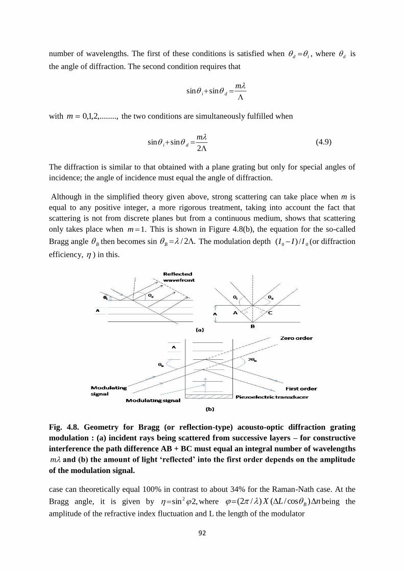
92
number of wavelengths. The first of these conditions is satisfied when id , where d is
the angle of diffraction. The second condition requires that
mdi sinsin
with ,........,2,1,0m the two conditions are simultaneously fulfilled when
2
sinsin
m
di (4.9)
The diffraction is similar to that obtained with a plane grating but only for special angles of
incidence; the angle of incidence must equal the angle of diffraction.
Although in the simplified theory given above, strong scattering can take place when m is
equal to any positive integer, a more rigorous treatment, taking into account the fact that
scattering is not from discrete planes but from a continuous medium, shows that scattering
only takes place when .1m This is shown in Figure 4.8(b), the equation for the so-called
Bragg angle B then becomes sin .2/ B The modulation depth 00 /)( III (or diffraction
efficiency, ) in this.
Fig. 4.8. Geometry for Bragg (or reflection-type) acousto-optic diffraction grating
modulation : (a) incident rays being scattered from successive layers – for constructive
interference the path difference AB + BC must equal an integral number of wavelengths
m and (b) the amount of light ‘reflected’ into the first order depends on the amplitude
of the modulation signal.
case can theoretically equal 100% in contrast to about 34% for the Raman-Nath case. At the
Bragg angle, it is given by ,2sin2 where nLX B )cos/()/2( being the
amplitude of the refractive index fluctuation and L the length of the modulator
93
The acoustic waves, which create the diffraction grating, are of course moving through the
medium and, as a consequence, the diffracted wave behaves as if it had been reflected
from a ‘mirror’ moving with the same velocity as the grating and, therefore, appears to
originate from a source moving at twice the mirror (or grating) velocity. Thus the frequency
of the reflected beam is changed by the Doppler effect and is given by
)/( 210 ncvv a
where av is the component of the velocity of the acoustic wave along (or a way from) the
original beam direction and n is the medium refractive index. The frequency shift is :
c
nvvv a 0
0
2
If the light is incident at an angle Di to the acoustic wave as shown in Figure 4.7(a) then
is the acoustic wave velocity. The frequency shift is then
c
nv da sin2 0 (4.10)
Combining Eqs. (4.9) and (4.10) and taking m = 1 gives a frequency shift of ,/ 0fora
where 0f is the acoustic wave frequency. This change in frequency can be used as the basis
of a frequency modulator.
The minimum time required to move from a condition where the acoustic wave
interacts with the light beam and ‘turns off’ the undiffracted light to a condition where there
is no diffraction is the transit time of the acoustic wave across the optical beam. This is
simply, from Figure 4.8, ,/min aBt where B is the optical beamwidth. Hence, the bandwidth
of the modulator is limited about Ba / . Commercial modulators have bandwidths of up to
50 MHz. This limitation is partly due to the frequency dependence of the acoustic losses of
available acousto-optic materials. At the present time only LiNbO3 and PbMoO4 appear to
have sufficiently low loss to have a reasonable prospect of being operated at appreciably
higher frequencies.
Acousto-optic modulators can in general be used for similar applications to electro-
optic modulators, though they are not so fast. On the other hand, because the electro-optic
effect usually requires voltages in the kilovolt range, the drive circuitry for modulators based
on this effect is much more expensive than for acousto-optic modulators, which operate with
a few volts.
4.10 Photodetector:
Photosensors or photodetectors are sensors of light or other electromagnetic energy. A
photo detector converts light signals that hit the junction into voltage or current. The
connection uses an illumination window with an anti-reflect coating to absorb the light
94
photons. This results in creation of electron-hole pairs in the depletion region. Photodiodes
and photo transistors are few examples of photo detectors. Solar cells are also similar to
photo detectors as they absorb light and turn it into energy.
(i) Types: Photodetectors may be classified by their mechanism for detection:
(i) Photoemission: Photons cause electrons to transition from the conduction band of a
material to free electrons in a vacuum or gas.
(ii) Photoelectric: Photons cause electrons to transition from the valence band to the
conduction band of a semiconductor.
(iii) Photovoltaic: Photons cause a voltage to develop across a depletion region of a
photovoltaic cell.
(iv) Thermal: Photons cause electrons to transition to mid-gap states then decay back to
lower bands, inducing phonon generation and thus heat.
(v) Polarization: Photons induce changes in polarization states of suitable materials, which
may lead to change in index of refraction or other polarization effects.
(vi) Photochemical: Photons induce a chemical change in a material.
(vii) Weak interaction effects: photons induce secondary effects such as in photon drag
detectors or gas pressure changes in Golay cells.
Photodetectors may be used in different configurations. Single sensors may detect overall
light levels. A 1-D array of photodetectors, as in a spectrophotometer or a Line scanner, may
be used to measure the distribution of light along a line. A 2-D array of photodetectors may
be used as an image sensor to form images from the pattern of light before it.
(ii) Properties: There are a number of performance metrics, also called figures of merit, by
which photodetectors are characterized and compared
(i) Spectral response: The response of a photodetector as a function of photon frequency.
(ii) Quantum efficiency: The number of carriers (electrons or holes) generated per photon.
(iii)Responsivity: The output current divided by total light power falling upon the
photodetector.
(iv) Noise-equivalent power: The amount of light power needed to generate a signal
comparable in size to the noise of the device.
(v) Detectivity: The square root of the detector area divided by the noise equivalent power.
(vi) Gain: The output current of a photodetector divided by the current directly produced by
the photons incident on the detectors, i.e., the built-in current gain.
(vii) Dark current: The current flowing through a photodetector even in the absence of
light.
(viii) Response time: The time needed for a photodetector to go from 10% to 90% of final
output.
95
(ix) Noise spectrum: The intrinsic noise voltage or current as a function of frequency. This
can be represented in the form of a noise spectral density.
4.11 Thermal Detectors: A thermal detector absorbs radiation and changes temperature.
Because the power in absorbed radiation is typically rather small (<10-7
W), the detector itself
should be small so that it has a low heat capacity.
A thermocouple is the joining of two dissimilar-metal or metal alloy wires or films. When
this occurs, a potential difference is formed between the other ends of the metals. Since
potential differences are temperature-dependent (called the Seebeck effect), temperature
values or changes in temperatures can be determined by calibration
A bolometer is a semiconductor or thin metal strip whose resistance decreases with
temperature. They are small, and typically painted black to better absorb radiation.
A Golay detector is a small pneumatic chamber filled with gas and covered with a thin
membrane. When radiation strikes the detector, the gas warms, increasing the internal
pressure and deforming the membrane. Deflection of the membrane can be measured
mechanically or optically.
A pyroelectric detector uses a crystal of a pyroelectric material, which has a strong
temperature-dependent electric polarization. The change in electric polarization causes a
measurable current, which changes fast enough to respond to the output of an interferometer.
The most common material used is deuterated triglycine sulfate, (dTGS). Lithium tantalate
(LiTaO3) and lead zinc titanate (PZT) are also used.
4.12 Photoconductor: The photoconductive device (Fig.4.9) is based on the decrease in the
resistance of certain semiconductor materials when they are exposed to both infrared and
visible radiation. The photoconductivity is the result of carrier excitation due to light
absorption and the figure of merit depends on the light absorption efficiency. The increase in
conductivity is due to an increase in the number of mobile charge carriers in the material.
Fig.4.9 Sketch of photoconductive device
Theory: Let us consider a photo conducting slab. It is simply a light sensitive semiconductor
material with ohmic contacts on both ends. When the material is illuminated with photons of
energy E ≥Eg electron hole pairs are generated and the electrical conductivity of the material
increases. Where Eg is the bandgap energy of the semiconductor material given by
96
Eg = hc / λ
Where λ is the wavelength of the incident photon.
Let I0 be the intensity of monochromatic light falling normally onto the slab. Then the
intensity of transmitted light I is given by
I = I0 exp ( -αD).
Where α is the absorption coefficient of the material and D is the thickness of the slab. Let L
and B be the length and breadth of the photoconductive slab respectively. Also let us assume
that the slab absorbs the entire light falling on it. Now the light energy falls on the sample per
sec is given by I0 BL, where I0 is the light energy falling per second on unit area of the slab.
Therefore the number of photons falling on the photoconductor per second
Let η- be the quantum efficiency of the absorption process. It is nothing but the fraction of
incident energy absorbed. Therefore the number of photons absorbed per second
Now the average generation rate of charge carriers is given by
,
Let ∆n and ∆ P be the excess electron and hole density per unit volume in the device. If τc is
the life time of charge carriers,Then the recombination rate
At equilibrium, the recombination rate = generation rate. Therefore ∆ p = ∆ n = rg τc. We
know the conductivity of a semi conducting material is . Under
illumination the conductivity will increase by an amount is
When a voltage is applied to the contacts, electrons and holes move in opposite directions
resulting in a photocurrent given by VL
BDi , Ver
L
BDi hecg )(
The quantum efficiency of a photoconductor device is defined by the term photoconductor
gain G. Photoconductive gain is defined as the ratio of rate of flow of electrons per second to
the rate of generation of electron hole pairs within the device.
hv
BLI0
hv
BLI0
hvBLD
BLIrg
0
hvD
Irg
0
cc
r
pnr
he epne .
he epne .
)( hene
)( hecg er
97
pairsholeelectronofgenerationofRate
electronsofflowofRateG
sec/
But rate of flow of electrons per sec = ∆i/e.
Rate of generation of electron hole pairs = rg BLD
,
The photoconductive gain G can be increased by increasing the voltage V and decreasing the
length, L of the device. The photoconductive gain can also be defined as the ratio of the
minority carriers life time and the transit time t.
i.e.,
Construction of photoconductive device: The four materials normally employed in
photoconductive devices are: Cadmium Sulphide (CdS), Cadmium Selenide (CdSe), lead
sulphide (PbS) and Thallium Sulphide (TlSIn a typical construction of photoconductive
device, thin film is deposited on an insulating substrate. The electrodes are formed by
evaporating metal such as gold through a mask to give comb -like pattern as shown in Fig
4.10. The geometry results in a relatively large area of sensitive surface and a small inter
electrode spacing. This helps the device to provide high sensitivity.
Fig. 4.10 Geometry of the photoconductive cell
When the device under forward bias is illuminated with light electron–hole pairs are
generated. The electron-hole pairs generated move in opposite directions. This results in a
photocurrent. The photoconductive cell has very high resistance in dark called dark
resistance. When illuminated the resistance falls. The spectral response of CdS cell is similar
to that of the human eye. The illumination characteristics of the cell is shown in Fig.4.11.
Desired characteristics of photoconductive materials.They are
i) High spectral sensitivity in the wavelength region of interest
ii) Higher quantum efficiency
iii) Higher photoconductive gain
iv) Higher speed of response and
v) lesser noise
BLDr
eiG
g
)(
2
)(
L
VG hec
tG c
98
(a) (b)
Fig.4.11 (a) Photoconductor in circuit (b) Spectral response of CdS cell
Materials:
(i) Cadmium sulfide (CdS) and Cadmium selenide (CdSe) :
These are highly sensitive in the visible region of radiation.They have high
photoconductive gains (103 to 104) but poor response time (about 50 ms). The response gets
reduced at higher illumination levels indicating the presence of traps.
(ii) Lead sulfide (PbS)
It has spectral responsitivity from 1 to 3.4 μm and hence very much suitable for
fabricating near-infrared detectors. It has maximum sensitivity in the region of 2 μm with
typical response time about 200 μs.
(iii) Indium antimonide (InSb)
These detectors have wavelength response extending out to 7 μm and exhibit response
times of around 50 ns.
(iv) Mercury cadmium telluride (HgxCd1-x Te)
This is an alloy composed of the semi-metal HgTe and the semi-conductor CdTe.
Semi-metals have overlapping valence and conduction bands. Depending on the composition
of alloy, a semiconductor can be formed with a bandgap varying between zero and 1.6eV.
Correspondingly the detector sensitivities lie in the range 5 to 14 μm. Photoconductive gains
of up to 500 are possible
Applications of photoconductivity devices They are,
• Light meters
• Infrared detectors
• TV cameras
• Voltage regulator
• Relays and
• Detecting ships and air crafts
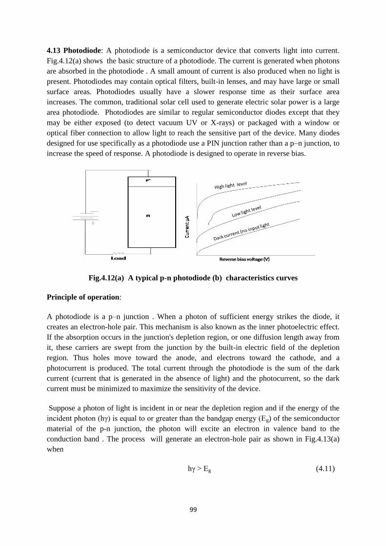
99
4.13 Photodiode: A photodiode is a semiconductor device that converts light into current.
Fig.4.12(a) shows the basic structure of a photodiode. The current is generated when photons
are absorbed in the photodiode . A small amount of current is also produced when no light is
present. Photodiodes may contain optical filters, built-in lenses, and may have large or small
surface areas. Photodiodes usually have a slower response time as their surface area
increases. The common, traditional solar cell used to generate electric solar power is a large
area photodiode. Photodiodes are similar to regular semiconductor diodes except that they
may be either exposed (to detect vacuum UV or X-rays) or packaged with a window or
optical fiber connection to allow light to reach the sensitive part of the device. Many diodes
designed for use specifically as a photodiode use a PIN junction rather than a p–n junction, to
increase the speed of response. A photodiode is designed to operate in reverse bias.
Fig.4.12(a) A typical p-n photodiode (b) characteristics curves
Principle of operation:
A photodiode is a p–n junction . When a photon of sufficient energy strikes the diode, it
creates an electron-hole pair. This mechanism is also known as the inner photoelectric effect.
If the absorption occurs in the junction's depletion region, or one diffusion length away from
it, these carriers are swept from the junction by the built-in electric field of the depletion
region. Thus holes move toward the anode, and electrons toward the cathode, and a
photocurrent is produced. The total current through the photodiode is the sum of the dark
current (current that is generated in the absence of light) and the photocurrent, so the dark
current must be minimized to maximize the sensitivity of the device.
Suppose a photon of light is incident in or near the depletion region and if the energy of the
incident photon (hγ) is equal to or greater than the bandgap energy (Eg) of the semiconductor
material of the p-n junction, the photon will excite an electron in valence band to the
conduction band . The process will generate an electron-hole pair as shown in Fig.4.13(a)
when
hγ > Eg (4.11)
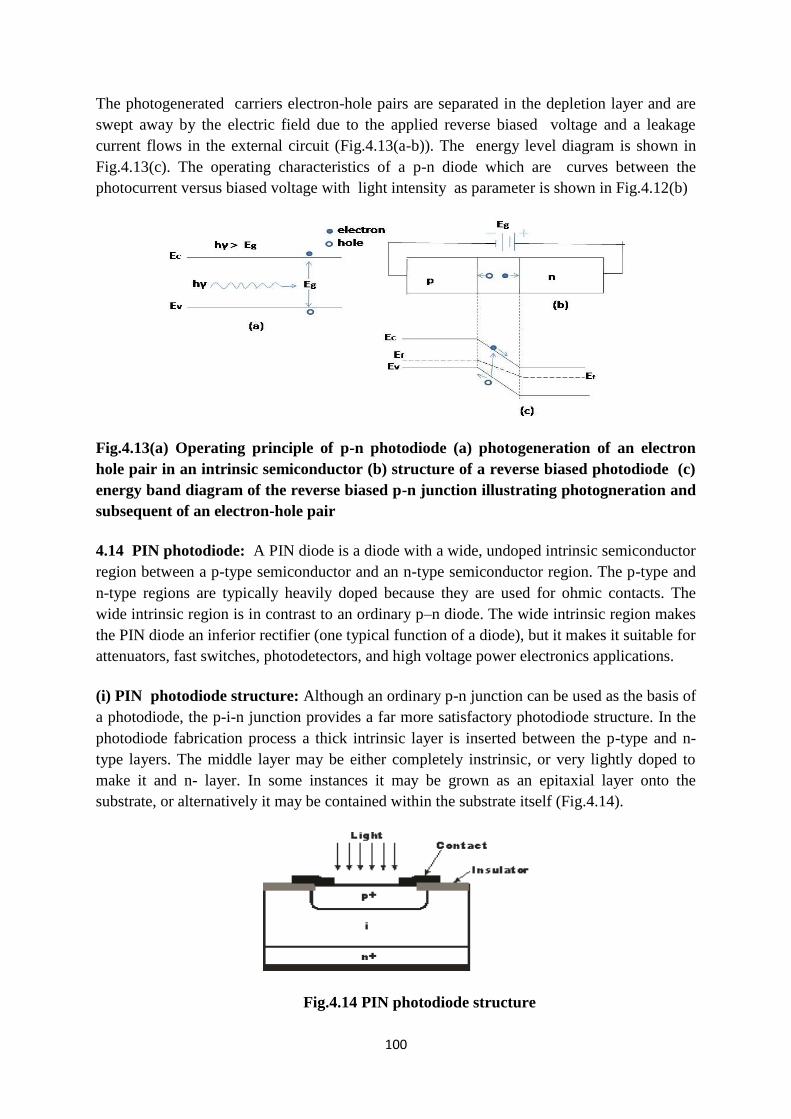
100
The photogenerated carriers electron-hole pairs are separated in the depletion layer and are
swept away by the electric field due to the applied reverse biased voltage and a leakage
current flows in the external circuit (Fig.4.13(a-b)). The energy level diagram is shown in
Fig.4.13(c). The operating characteristics of a p-n diode which are curves between the
photocurrent versus biased voltage with light intensity as parameter is shown in Fig.4.12(b)
Fig.4.13(a) Operating principle of p-n photodiode (a) photogeneration of an electron
hole pair in an intrinsic semiconductor (b) structure of a reverse biased photodiode (c)
energy band diagram of the reverse biased p-n junction illustrating photogneration and
subsequent of an electron-hole pair
4.14 PIN photodiode: A PIN diode is a diode with a wide, undoped intrinsic semiconductor
region between a p-type semiconductor and an n-type semiconductor region. The p-type and
n-type regions are typically heavily doped because they are used for ohmic contacts. The
wide intrinsic region is in contrast to an ordinary p–n diode. The wide intrinsic region makes
the PIN diode an inferior rectifier (one typical function of a diode), but it makes it suitable for
attenuators, fast switches, photodetectors, and high voltage power electronics applications.
(i) PIN photodiode structure: Although an ordinary p-n junction can be used as the basis of
a photodiode, the p-i-n junction provides a far more satisfactory photodiode structure. In the
photodiode fabrication process a thick intrinsic layer is inserted between the p-type and n-
type layers. The middle layer may be either completely instrinsic, or very lightly doped to
make it and n- layer. In some instances it may be grown as an epitaxial layer onto the
substrate, or alternatively it may be contained within the substrate itself (Fig.4.14).
Fig.4.14 PIN photodiode structure
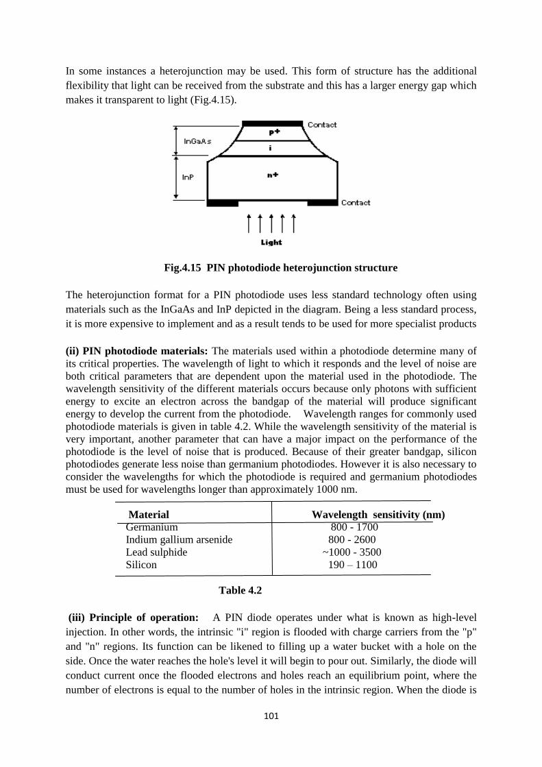
101
In some instances a heterojunction may be used. This form of structure has the additional
flexibility that light can be received from the substrate and this has a larger energy gap which
makes it transparent to light (Fig.4.15).
Fig.4.15 PIN photodiode heterojunction structure
The heterojunction format for a PIN photodiode uses less standard technology often using
materials such as the InGaAs and InP depicted in the diagram. Being a less standard process,
it is more expensive to implement and as a result tends to be used for more specialist products
(ii) PIN photodiode materials: The materials used within a photodiode determine many of
its critical properties. The wavelength of light to which it responds and the level of noise are
both critical parameters that are dependent upon the material used in the photodiode. The
wavelength sensitivity of the different materials occurs because only photons with sufficient
energy to excite an electron across the bandgap of the material will produce significant
energy to develop the current from the photodiode. Wavelength ranges for commonly used
photodiode materials is given in table 4.2. While the wavelength sensitivity of the material is
very important, another parameter that can have a major impact on the performance of the
photodiode is the level of noise that is produced. Because of their greater bandgap, silicon
photodiodes generate less noise than germanium photodiodes. However it is also necessary to
consider the wavelengths for which the photodiode is required and germanium photodiodes
must be used for wavelengths longer than approximately 1000 nm.
Material Wavelength sensitivity (nm)
Germanium 800 - 1700
Indium gallium arsenide 800 - 2600
Lead sulphide ~1000 - 3500
Silicon 190 – 1100
Table 4.2
(iii) Principle of operation: A PIN diode operates under what is known as high-level
injection. In other words, the intrinsic "i" region is flooded with charge carriers from the "p"
and "n" regions. Its function can be likened to filling up a water bucket with a hole on the
side. Once the water reaches the hole's level it will begin to pour out. Similarly, the diode will
conduct current once the flooded electrons and holes reach an equilibrium point, where the
number of electrons is equal to the number of holes in the intrinsic region. When the diode is
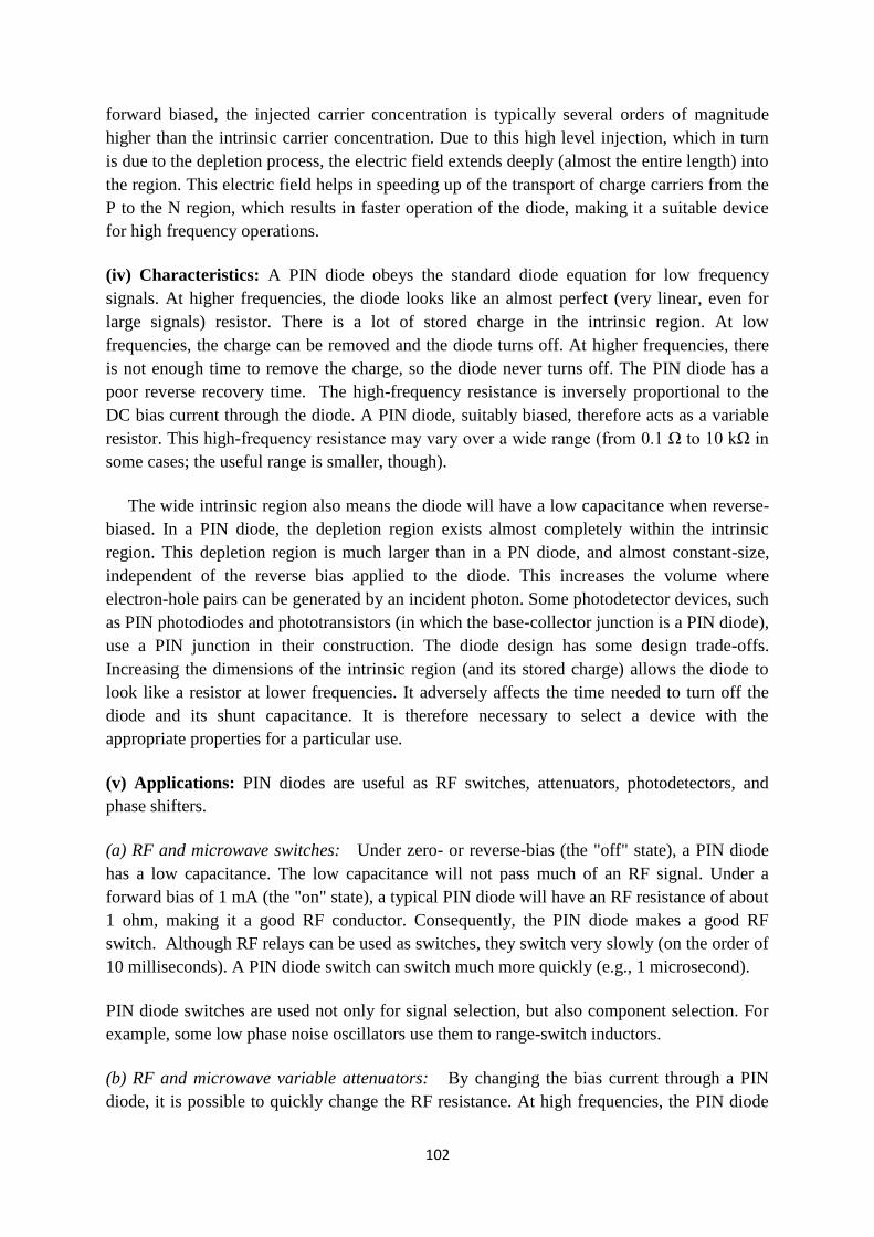
102
forward biased, the injected carrier concentration is typically several orders of magnitude
higher than the intrinsic carrier concentration. Due to this high level injection, which in turn
is due to the depletion process, the electric field extends deeply (almost the entire length) into
the region. This electric field helps in speeding up of the transport of charge carriers from the
P to the N region, which results in faster operation of the diode, making it a suitable device
for high frequency operations.
(iv) Characteristics: A PIN diode obeys the standard diode equation for low frequency
signals. At higher frequencies, the diode looks like an almost perfect (very linear, even for
large signals) resistor. There is a lot of stored charge in the intrinsic region. At low
frequencies, the charge can be removed and the diode turns off. At higher frequencies, there
is not enough time to remove the charge, so the diode never turns off. The PIN diode has a
poor reverse recovery time. The high-frequency resistance is inversely proportional to the
DC bias current through the diode. A PIN diode, suitably biased, therefore acts as a variable
resistor. This high-frequency resistance may vary over a wide range (from 0.1 Ω to 10 kΩ in
some cases; the useful range is smaller, though).
The wide intrinsic region also means the diode will have a low capacitance when reverse-
biased. In a PIN diode, the depletion region exists almost completely within the intrinsic
region. This depletion region is much larger than in a PN diode, and almost constant-size,
independent of the reverse bias applied to the diode. This increases the volume where
electron-hole pairs can be generated by an incident photon. Some photodetector devices, such
as PIN photodiodes and phototransistors (in which the base-collector junction is a PIN diode),
use a PIN junction in their construction. The diode design has some design trade-offs.
Increasing the dimensions of the intrinsic region (and its stored charge) allows the diode to
look like a resistor at lower frequencies. It adversely affects the time needed to turn off the
diode and its shunt capacitance. It is therefore necessary to select a device with the
appropriate properties for a particular use.
(v) Applications: PIN diodes are useful as RF switches, attenuators, photodetectors, and
phase shifters.
(a) RF and microwave switches: Under zero- or reverse-bias (the "off" state), a PIN diode
has a low capacitance. The low capacitance will not pass much of an RF signal. Under a
forward bias of 1 mA (the "on" state), a typical PIN diode will have an RF resistance of about
1 ohm, making it a good RF conductor. Consequently, the PIN diode makes a good RF
switch. Although RF relays can be used as switches, they switch very slowly (on the order of
10 milliseconds). A PIN diode switch can switch much more quickly (e.g., 1 microsecond).
PIN diode switches are used not only for signal selection, but also component selection. For
example, some low phase noise oscillators use them to range-switch inductors.
(b) RF and microwave variable attenuators: By changing the bias current through a PIN
diode, it is possible to quickly change the RF resistance. At high frequencies, the PIN diode
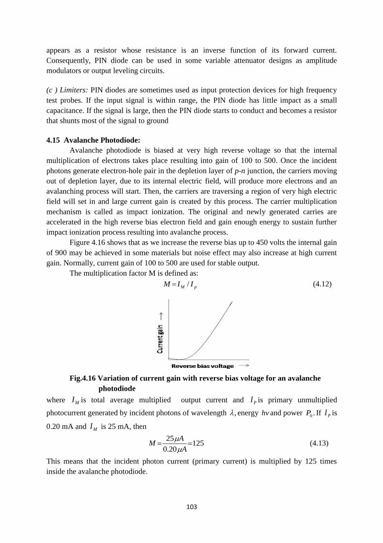
103
appears as a resistor whose resistance is an inverse function of its forward current.
Consequently, PIN diode can be used in some variable attenuator designs as amplitude
modulators or output leveling circuits.
(c ) Limiters: PIN diodes are sometimes used as input protection devices for high frequency
test probes. If the input signal is within range, the PIN diode has little impact as a small
capacitance. If the signal is large, then the PIN diode starts to conduct and becomes a resistor
that shunts most of the signal to ground
4.15 Avalanche Photodiode:
Avalanche photodiode is biased at very high reverse voltage so that the internal
multiplication of electrons takes place resulting into gain of 100 to 500. Once the incident
photons generate electron-hole pair in the depletion layer of p-n junction, the carriers moving
out of depletion layer, due to its internal electric field, will produce more electrons and an
avalanching process will start. Then, the carriers are traversing a region of very high electric
field will set in and large current gain is created by this process. The carrier multiplication
mechanism is called as impact ionization. The original and newly generated carries are
accelerated in the high reverse bias electron field and gain enough energy to sustain further
impact ionization process resulting into avalanche process.
Figure 4.16 shows that as we increase the reverse bias up to 450 volts the internal gain
of 900 may be achieved in some materials but noise effect may also increase at high current
gain. Normally, current gain of 100 to 500 are used for stable output.
The multiplication factor M is defined as:
pM IIM / (4.12)
Fig.4.16 Variation of current gain with reverse bias voltage for an avalanche
photodiode
where MI is total average multiplied output current and PI is primary unmultiplied
photocurrent generated by incident photons of wavelength , energy hv and power .0P If PI is
0.20 mA and MI is 25 mA, then
12520.0
25
A
AM
(4.13)
This means that the incident photon current (primary current) is multiplied by 125 times
inside the avalanche photodiode.
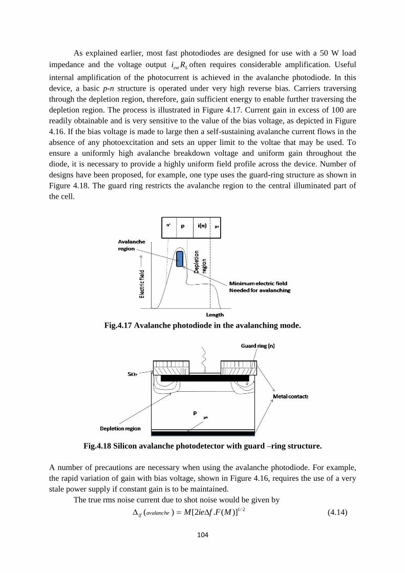
104
As explained earlier, most fast photodiodes are designed for use with a 50 W load
impedance and the voltage output Lext Ri often requires considerable amplification. Useful
internal amplification of the photocurrent is achieved in the avalanche photodiode. In this
device, a basic p-n structure is operated under very high reverse bias. Carriers traversing
through the depletion region, therefore, gain sufficient energy to enable further traversing the
depletion region. The process is illustrated in Figure 4.17. Current gain in excess of 100 are
readily obtainable and is very sensitive to the value of the bias voltage, as depicted in Figure
4.16. If the bias voltage is made to large then a self-sustaining avalanche current flows in the
absence of any photoexcitation and sets an upper limit to the voltae that may be used. To
ensure a uniformly high avalanche breakdown voltage and uniform gain throughout the
diode, it is necessary to provide a highly uniform field profile across the device. Number of
designs have been proposed, for example, one type uses the guard-ring structure as shown in
Figure 4.18. The guard ring restricts the avalanche region to the central illuminated part of
the cell.
Fig.4.17 Avalanche photodiode in the avalanching mode.
Fig.4.18 Silicon avalanche photodetector with guard –ring structure.
A number of precautions are necessary when using the avalanche photodiode. For example,
the rapid variation of gain with bias voltage, shown in Figure 4.16, requires the use of a very
stale power supply if constant gain is to be maintained.
The true rms noise current due to shot noise would be given by
2/1)](.2[)( MFfieMavalancheif (4.14)
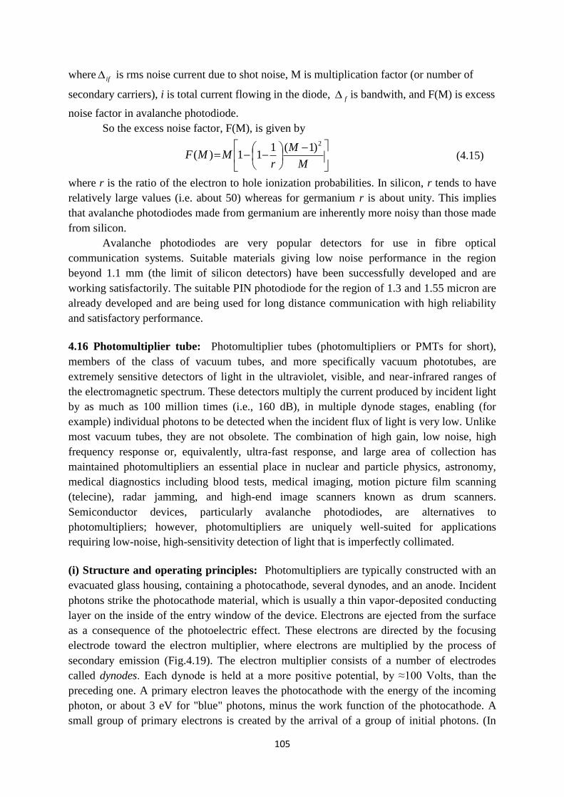
105
where if is rms noise current due to shot noise, M is multiplication factor (or number of
secondary carriers), i is total current flowing in the diode, f is bandwith, and F(M) is excess
noise factor in avalanche photodiode.
So the excess noise factor, F(M), is given by
M
M
rMMF
2)1(111)( (4.15)
where r is the ratio of the electron to hole ionization probabilities. In silicon, r tends to have
relatively large values (i.e. about 50) whereas for germanium r is about unity. This implies
that avalanche photodiodes made from germanium are inherently more noisy than those made
from silicon.
Avalanche photodiodes are very popular detectors for use in fibre optical
communication systems. Suitable materials giving low noise performance in the region
beyond 1.1 mm (the limit of silicon detectors) have been successfully developed and are
working satisfactorily. The suitable PIN photodiode for the region of 1.3 and 1.55 micron are
already developed and are being used for long distance communication with high reliability
and satisfactory performance.
4.16 Photomultiplier tube: Photomultiplier tubes (photomultipliers or PMTs for short),
members of the class of vacuum tubes, and more specifically vacuum phototubes, are
extremely sensitive detectors of light in the ultraviolet, visible, and near-infrared ranges of
the electromagnetic spectrum. These detectors multiply the current produced by incident light
by as much as 100 million times (i.e., 160 dB), in multiple dynode stages, enabling (for
example) individual photons to be detected when the incident flux of light is very low. Unlike
most vacuum tubes, they are not obsolete. The combination of high gain, low noise, high
frequency response or, equivalently, ultra-fast response, and large area of collection has
maintained photomultipliers an essential place in nuclear and particle physics, astronomy,
medical diagnostics including blood tests, medical imaging, motion picture film scanning
(telecine), radar jamming, and high-end image scanners known as drum scanners.
Semiconductor devices, particularly avalanche photodiodes, are alternatives to
photomultipliers; however, photomultipliers are uniquely well-suited for applications
requiring low-noise, high-sensitivity detection of light that is imperfectly collimated.
(i) Structure and operating principles: Photomultipliers are typically constructed with an
evacuated glass housing, containing a photocathode, several dynodes, and an anode. Incident
photons strike the photocathode material, which is usually a thin vapor-deposited conducting
layer on the inside of the entry window of the device. Electrons are ejected from the surface
as a consequence of the photoelectric effect. These electrons are directed by the focusing
electrode toward the electron multiplier, where electrons are multiplied by the process of
secondary emission (Fig.4.19). The electron multiplier consists of a number of electrodes
called dynodes. Each dynode is held at a more positive potential, by ≈100 Volts, than the
preceding one. A primary electron leaves the photocathode with the energy of the incoming
photon, or about 3 eV for "blue" photons, minus the work function of the photocathode. A
small group of primary electrons is created by the arrival of a group of initial photons. (In
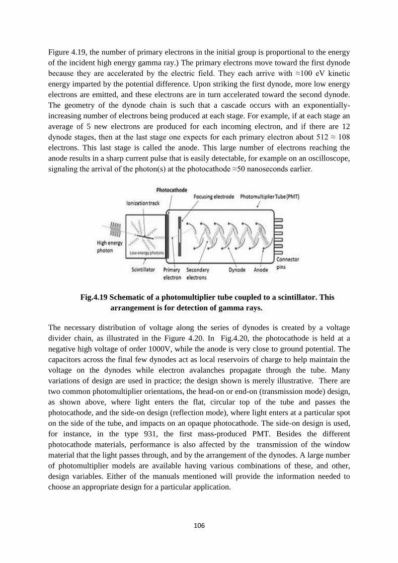
106
Figure 4.19, the number of primary electrons in the initial group is proportional to the energy
of the incident high energy gamma ray.) The primary electrons move toward the first dynode
because they are accelerated by the electric field. They each arrive with ≈100 eV kinetic
energy imparted by the potential difference. Upon striking the first dynode, more low energy
electrons are emitted, and these electrons are in turn accelerated toward the second dynode.
The geometry of the dynode chain is such that a cascade occurs with an exponentially-
increasing number of electrons being produced at each stage. For example, if at each stage an
average of 5 new electrons are produced for each incoming electron, and if there are 12
dynode stages, then at the last stage one expects for each primary electron about 512 ≈ 108
electrons. This last stage is called the anode. This large number of electrons reaching the
anode results in a sharp current pulse that is easily detectable, for example on an oscilloscope,
signaling the arrival of the photon(s) at the photocathode ≈50 nanoseconds earlier.
Fig.4.19 Schematic of a photomultiplier tube coupled to a scintillator. This
arrangement is for detection of gamma rays.
The necessary distribution of voltage along the series of dynodes is created by a voltage
divider chain, as illustrated in the Figure 4.20. In Fig.4.20, the photocathode is held at a
negative high voltage of order 1000V, while the anode is very close to ground potential. The
capacitors across the final few dynodes act as local reservoirs of charge to help maintain the
voltage on the dynodes while electron avalanches propagate through the tube. Many
variations of design are used in practice; the design shown is merely illustrative. There are
two common photomultiplier orientations, the head-on or end-on (transmission mode) design,
as shown above, where light enters the flat, circular top of the tube and passes the
photocathode, and the side-on design (reflection mode), where light enters at a particular spot
on the side of the tube, and impacts on an opaque photocathode. The side-on design is used,
for instance, in the type 931, the first mass-produced PMT. Besides the different
photocathode materials, performance is also affected by the transmission of the window
material that the light passes through, and by the arrangement of the dynodes. A large number
of photomultiplier models are available having various combinations of these, and other,
design variables. Either of the manuals mentioned will provide the information needed to
choose an appropriate design for a particular application.
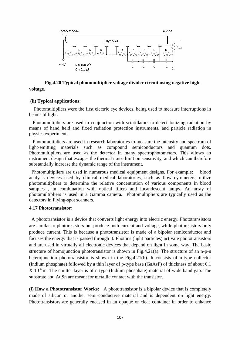
107
Fig.4.20 Typical photomultiplier voltage divider circuit using negative high
voltage.
(ii) Typical applications:
Photomultipliers were the first electric eye devices, being used to measure interruptions in
beams of light.
Photomultipliers are used in conjunction with scintillators to detect Ionizing radiation by
means of hand held and fixed radiation protection instruments, and particle radiation in
physics experiments.
Photomultipliers are used in research laboratories to measure the intensity and spectrum of
light-emitting materials such as compound semiconductors and quantum dots.
Photomultipliers are used as the detector in many spectrophotometers. This allows an
instrument design that escapes the thermal noise limit on sensitivity, and which can therefore
substantially increase the dynamic range of the instrument.
Photomultipliers are used in numerous medical equipment designs. For example: blood
analysis devices used by clinical medical laboratories, such as flow cytometers, utilize
photomultipliers to determine the relative concentration of various components in blood
samples , in combination with optical filters and incandescent lamps. An array of
photomultipliers is used in a Gamma camera. Photomultipliers are typically used as the
detectors in Flying-spot scanners.
4.17 Phototransistor:
A phototransistor is a device that converts light energy into electric energy. Phototransistors
are similar to photoresistors but produce both current and voltage, while photoresistors only
produce current. This is because a phototransistor is made of a bipolar semiconductor and
focuses the energy that is passed through it. Photons (light particles) activate phototransistors
and are used in virtually all electronic devices that depend on light in some way. The basic
structure of homojunction phototransistor is shown in Fig.4.21(a). The structure of an n-p-n
heterojunction phototransistor is shown in the Fig.4.21(b). It consists of n-type collector
(Indium phosphate) followed by a thin layer of p-type base (GaAsP) of thickness of about 0.1
X 10-6
m. The emitter layer is of n-type (Indium phosphate) material of wide band gap. The
substrate and AuSn are meant for metallic contact with the transistor.
(i) How a Phototransistor Works: A phototransistor is a bipolar device that is completely
made of silicon or another semi-conductive material and is dependent on light energy.
Phototransistors are generally encased in an opaque or clear container in order to enhance
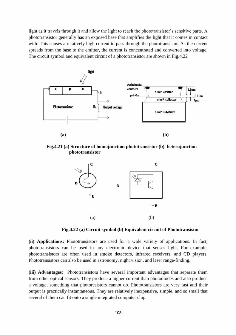
108
light as it travels through it and allow the light to reach the phototransistor’s sensitive parts. A
phototransistor generally has an exposed base that amplifies the light that it comes in contact
with. This causes a relatively high current to pass through the phototransistor. As the current
spreads from the base to the emitter, the current is concentrated and converted into voltage.
The circuit symbol and equivalent circuit of a phototransistor are shown in Fig.4.22
(a) (b)
Fig.4.21 (a) Structure of homojunction phototransistor (b) heterojunction
phototransistor
(a) (b)
Fig.4.22 (a) Circuit symbol (b) Equivalent circuit of Phototransistor
(ii) Applications: Phototransistors are used for a wide variety of applications. In fact,
phototransistors can be used in any electronic device that senses light. For example,
phototransistors are often used in smoke detectors, infrared receivers, and CD players.
Phototransistors can also be used in astronomy, night vision, and laser range-finding.
(iii) Advantages: Phototransistors have several important advantages that separate them
from other optical sensors. They produce a higher current than photodiodes and also produce
a voltage, something that photoresistors cannot do. Phototransistors are very fast and their
output is practically instantaneous. They are relatively inexpensive, simple, and so small that
several of them can fit onto a single integrated computer chip.
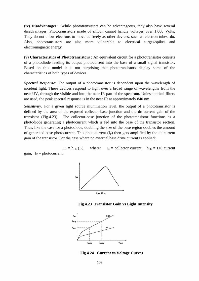
109
(iv) Disadvantages: While phototransistors can be advantageous, they also have several
disadvantages. Phototransistors made of silicon cannot handle voltages over 1,000 Volts.
They do not allow electrons to move as freely as other devices, such as electron tubes, do.
Also, phototransistors are also more vulnerable to electrical surges/spikes and
electromagnetic energy.
(v) Characteristics of Phototransistors : An equivalent circuit for a phototransistor consists
of a photodiode feeding its output photocurrent into the base of a small signal transistor.
Based on this model it is not surprising that phototransistors display some of the
characteristics of both types of devices.
Spectral Response: The output of a phototransistor is dependent upon the wavelength of
incident light. These devices respond to light over a broad range of wavelengths from the
near UV, through the visible and into the near IR part of the spectrum. Unless optical filters
are used, the peak spectral response is in the near IR at approximately 840 nm.
Sensitivity: For a given light source illumination level, the output of a phototransistor is
defined by the area of the exposed collector-base junction and the dc current gain of the
transistor (Fig.4.23) . The collector-base junction of the phototransistor functions as a
photodiode generating a photocurrent which is fed into the base of the transistor section.
Thus, like the case for a photodiode, doubling the size of the base region doubles the amount
of generated base photocurrent. This photocurrent (IP) then gets amplified by the dc current
gain of the transistor. For the case where no external base drive current is applied:
IC = hFE (IP), where: IC = collector current, hFE = DC current
gain, IP = photocurrent.
Fig.4.23 Transistor Gain vs Light Intensity
Fig.4.24 Current vs Voltage Curves
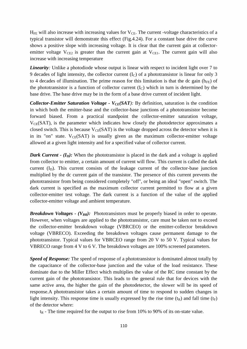
110
HFE will also increase with increasing values for VCE. The current -voltage characteristics of a
typical transistor will demonstrate this effect (Fig.4.24). For a constant base drive the curve
shows a positive slope with increasing voltage. It is clear that the current gain at collector-
emitter voltage VCE2 is greater than the current gain at VCE1. The current gain will also
increase with increasing temperature
Linearity: Unlike a photodiode whose output is linear with respect to incident light over 7 to
9 decades of light intensity, the collector current (IC) of a phototransistor is linear for only 3
to 4 decades of illumination. The prime reason for this limitation is that the dc gain (hFE) of
the phototransistor is a function of collector current (IC) which in turn is determined by the
base drive. The base drive may be in the form of a base drive current of incident light.
Collector-Emitter Saturation Voltage - VCE(SAT): By definition, saturation is the condition
in which both the emitter-base and the collector-base junctions of a phototransistor become
forward biased. From a practical standpoint the collector-emitter saturation voltage,
VCE(SAT), is the parameter which indicates how closely the photodetector approximates a
closed switch. This is because VCE(SAT) is the voltage dropped across the detector when it is
in its "on" state. VCE(SAT) is usually given as the maximum collector-emitter voltage
allowed at a given light intensity and for a specified value of collector current.
Dark Current - (ID): When the phototransistor is placed in the dark and a voltage is applied
from collector to emitter, a certain amount of current will flow. This current is called the dark
current (ID). This current consists of the leakage current of the collector-base junction
multiplied by the dc current gain of the transistor. The presence of this current prevents the
phototransistor from being considered completely "off", or being an ideal "open" switch. The
dark current is specified as the maximum collector current permitted to flow at a given
collector-emitter test voltage. The dark current is a function of the value of the applied
collector-emitter voltage and ambient temperature.
Breakdown Voltages - (VBR): Phototransistors must be properly biased in order to operate.
However, when voltages are applied to the phototransistor, care must be taken not to exceed
the collector-emitter breakdown voltage (VBRCEO) or the emitter-collector breakdown
voltage (VBRECO). Exceeding the breakdown voltages cause permanent damage to the
phototransistor. Typical values for VBRCEO range from 20 V to 50 V. Typical values for
VBRECO range from 4 V to 6 V. The breakdown voltages are 100% screened parameters.
Speed of Response: The speed of response of a phototransistor is dominated almost totally by
the capacitance of the collector-base junction and the value of the load resistance. These
dominate due to the Miller Effect which multiplies the value of the RC time constant by the
current gain of the phototransistor. This leads to the general rule that for devices with the
same active area, the higher the gain of the photodetector, the slower will be its speed of
response.A phototransistor takes a certain amount of time to respond to sudden changes in
light intensity. This response time is usually expressed by the rise time (tR) and fall time (tF)
of the detector where:
tR - The time required for the output to rise from 10% to 90% of its on-state value.
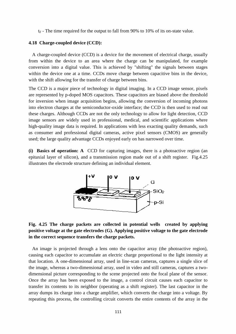
111
tF - The time required for the output to fall from 90% to 10% of its on-state value.
4.18 Charge-coupled device (CCD):
A charge-coupled device (CCD) is a device for the movement of electrical charge, usually
from within the device to an area where the charge can be manipulated, for example
conversion into a digital value. This is achieved by "shifting" the signals between stages
within the device one at a time. CCDs move charge between capacitive bins in the device,
with the shift allowing for the transfer of charge between bins.
The CCD is a major piece of technology in digital imaging. In a CCD image sensor, pixels
are represented by p-doped MOS capacitors. These capacitors are biased above the threshold
for inversion when image acquisition begins, allowing the conversion of incoming photons
into electron charges at the semiconductor-oxide interface; the CCD is then used to read out
these charges. Although CCDs are not the only technology to allow for light detection, CCD
image sensors are widely used in professional, medical, and scientific applications where
high-quality image data is required. In applications with less exacting quality demands, such
as consumer and professional digital cameras, active pixel sensors (CMOS) are generally
used; the large quality advantage CCDs enjoyed early on has narrowed over time.
(i) Basics of operation: A CCD for capturing images, there is a photoactive region (an
epitaxial layer of silicon), and a transmission region made out of a shift register. Fig.4.25
illustrates the electrode structure defining an individual element.
Fig. 4.25 The charge packets are collected in potential wells created by applying
positive voltage at the gate electrodes (G). Applying positive voltage to the gate electrode
in the correct sequence transfers the charge packets.
An image is projected through a lens onto the capacitor array (the photoactive region),
causing each capacitor to accumulate an electric charge proportional to the light intensity at
that location. A one-dimensional array, used in line-scan cameras, captures a single slice of
the image, whereas a two-dimensional array, used in video and still cameras, captures a two-
dimensional picture corresponding to the scene projected onto the focal plane of the sensor.
Once the array has been exposed to the image, a control circuit causes each capacitor to
transfer its contents to its neighbor (operating as a shift register). The last capacitor in the
array dumps its charge into a charge amplifier, which converts the charge into a voltage. By
repeating this process, the controlling circuit converts the entire contents of the array in the
112
semiconductor to a sequence of voltages. In a digital device, these voltages are then sampled,
digitized, and usually stored in memory; in an analog device (such as an analog video
camera), they are processed into a continuous analog signal (e.g. by feeding the output of the
charge amplifier into a low-pass filter), which is then processed and fed out to other circuits
for transmission, recording, or other processing.
(ii) Architecture: The CCD image sensors can be implemented in several different
architectures. The most common are full-frame, frame-transfer, and interline. The
distinguishing characteristic of each of these architectures is their approach to the problem of
shuttering. In a full-frame device, all of the image area is active, and there is no electronic
shutter. A mechanical shutter must be added to this type of sensor or the image smears as the
device is clocked or read out. With a frame-transfer CCD, half of the silicon area is covered
by an opaque mask (typically aluminum). The image can be quickly transferred from the
image area to the opaque area or storage region with acceptable smear of a few percent. That
image can then be read out slowly from the storage region while a new image is integrating
or exposing in the active area. Frame-transfer devices typically do not require a mechanical
shutter and were a common architecture for early solid-state broadcast cameras. The
downside to the frame-transfer architecture is that it requires twice the silicon real estate of an
equivalent full-frame device; hence, it costs roughly twice as much. The interline architecture
extends this concept one step further and masks every other column of the image sensor for
storage. In this device, only one pixel shift has to occur to transfer from image area to storage
area; thus, shutter times can be less than a microsecond and smear is essentially eliminated.
(iii) Use in astronomy:
Due to the high quantum efficiencies of CCDs (for a quantum efficiency of 100%, one
count equals one photon), linearity of their outputs, ease of use compared to photographic
plates, and a variety of other reasons, CCDs were very rapidly adopted by astronomers for
nearly all UV-to-infrared applications.
Thermal noise and cosmic rays may alter the pixels in the CCD array. To counter such
effects, astronomers take several exposures with the CCD shutter closed and opened. The
average of images taken with the shutter closed is necessary to lower the random noise. Once
developed, the dark frame average image is then subtracted from the open-shutter image to
remove the dark current and other systematic defects (dead pixels, hot pixels, etc.) in the
CCD.
The Hubble Space Telescope, in particular, has a highly developed series of steps (“data
reduction pipeline”) to convert the raw CCD data to useful images. CCD cameras used in
astrophotography often require sturdy mounts to cope with vibrations from wind and other
sources, along with the tremendous weight of most imaging platforms. Array of 30 CCDs
used on Sloan Digital Sky Survey telescope imaging camera, an example of "drift-scanning."
An interesting unusual astronomical application of CCDs, called drift-scanning, uses a CCD
to make a fixed telescope behave like a tracking telescope and follow the motion of the sky.
113
The charges in the CCD are transferred and read in a direction parallel to the motion of the
sky, and at the same speed. In this way, the telescope can image a larger region of the sky
than its normal field of view.
Digital color cameras generally use a Bayer mask over the CCD. Each square of four pixels
has one filtered red, one blue, and two green (the human eye is more sensitive to green than
either red or blue). The result of this is that luminance information is collected at every pixel,
but the color resolution is lower than the luminance resolution. Better color separation can be
reached by three-CCD devices (3CCD) and a dichroic beam splitter prism, that splits the
image into red, green and blue components. Each of the three CCDs is arranged to respond to
a particular color. Many professional video camcorders, and some semi-professional
camcorders, use this technique, although developments in competing CMOS technology have
made CMOS sensors, both with beam-splitters and bayer filters, increasingly popular in high-
end video and digital cinema cameras. Another advantage of 3CCD over a Bayer mask
device is higher quantum efficiency (and therefore higher light sensitivity for a given aperture
size). This is because in a 3CCD device most of the light entering the aperture is captured by
a sensor, while a Bayer mask absorbs a high proportion (about 2/3) of the light falling on
each CCD pixel.
4.19 Solar cell:
A solar cell, or photovoltaic is an electrical device that converts the energy of light directly
into electricity by the photovoltaic effect, which is a physical and chemical phenomenon. It is
a form of photoelectric cell, defined as a device whose electrical characteristics, such as
current, voltage, or resistance, vary when exposed to light. Solar cells are the building blocks
of photovoltaic modules, otherwise known as solar panels. Solar cells are described as being
photovoltaic irrespective of whether the source is sunlight or an artificial light. They are used
as a photodetector (for example infrared detectors), detecting light or other electromagnetic
radiation near the visible range, or measuring light intensity.
Solar cells can be classified into first, second and third generation cells. The first
generation cells—also called conventional, traditional or wafer-based cells—are made of
crystalline silicon, the commercially predominant PV technology, that includes materials
such as polysilicon and monocrystalline silicon. Second generation cells are thin film solar
cells, that include amorphous silicon, CdTe and CIGS cells and are commercially significant
in utility-scale photovoltaic power stations, building integrated photovoltaics or in small
stand-alone power system. The third generation of solar cells includes a number of thin-film
technologies often described as emerging photovoltaics—most of them have not yet been
commercially applied and are still in the research or development phase. Many use organic
materials, often organometallic compounds as well as inorganic substances. Despite the fact
that their efficiencies had been low and the stability of the absorber material was often too
short for commercial applications, there is a lot of research invested into these technologies
as they promise to achieve the goal of producing low-cost, high-efficiency solar cells.
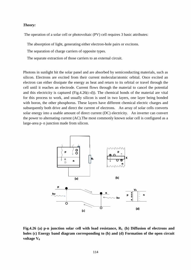
114
Theory:
The operation of a solar cell or photovoltaic (PV) cell requires 3 basic attributes:
The absorption of light, generating either electron-hole pairs or excitons.
The separation of charge carriers of opposite types.
The separate extraction of those carriers to an external circuit.
Photons in sunlight hit the solar panel and are absorbed by semiconducting materials, such as
silicon. Electrons are excited from their current molecular/atomic orbital. Once excited an
electron can either dissipate the energy as heat and return to its orbital or travel through the
cell until it reaches an electrode. Current flows through the material to cancel the potential
and this electricity is captured (Fig.4.26(c-d)). The chemical bonds of the material are vital
for this process to work, and usually silicon is used in two layers, one layer being bonded
with boron, the other phosphorus. These layers have different chemical electric charges and
subsequently both drive and direct the current of electrons. An array of solar cells converts
solar energy into a usable amount of direct current (DC) electricity. An inverter can convert
the power to alternating current (AC).The most commonly known solar cell is configured as a
large-area p–n junction made from silicon.
Fig.4.26 (a) p-n junction solar cell with load resistance, RL (b) Diffusion of electrons and
holes (c) Energy band diagram corresponding to (b) and (d) Formation of the open circuit
voltage V0
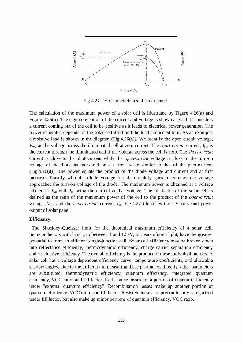
115
Fig.4.27 I-V Characteristics of solar panel
The calculation of the maximum power of a solar cell is illustrated by Figure 4.26(a) and
Figure 4.26(b). The sign convention of the current and voltage is shown as well. It considers
a current coming out of the cell to be positive as it leads to electrical power generation. The
power generated depends on the solar cell itself and the load connected to it. As an example,
a resistive load is shown in the diagram (Fig.4.26(a)). We identify the open-circuit voltage,
Voc, as the voltage across the illuminated cell at zero current. The short-circuit current, Isc, is
the current through the illuminated cell if the voltage across the cell is zero. The short-circuit
current is close to the photocurrent while the open-circuit voltage is close to the turn-on
voltage of the diode as measured on a current scale similar to that of the photocurrent
(Fig.4.26(d)). The power equals the product of the diode voltage and current and at first
increases linearly with the diode voltage but then rapidly goes to zero as the voltage
approaches the turn-on voltage of the diode. The maximum power is obtained at a voltage
labeled as Vm with Im being the current at that voltage. The fill factor of the solar cell is
defined as the ratio of the maximum power of the cell to the product of the open-circuit
voltage, Voc, and the short-circuit current, Isc. Fig.4.27 illustrates the I-V curveand power
output of solar panel.
Efficiency:
The Shockley-Queisser limit for the theoretical maximum efficiency of a solar cell.
Semiconductors with band gap between 1 and 1.5eV, or near-infrared light, have the greatest
potential to form an efficient single-junction cell. Solar cell efficiency may be broken down
into reflectance efficiency, thermodynamic efficiency, charge carrier separation efficiency
and conductive efficiency. The overall efficiency is the product of these individual metrics. A
solar cell has a voltage dependent efficiency curve, temperature coefficients, and allowable
shadow angles. Due to the difficulty in measuring these parameters directly, other parameters
are substituted: thermodynamic efficiency, quantum efficiency, integrated quantum
efficiency, VOC ratio, and fill factor. Reflectance losses are a portion of quantum efficiency
under "external quantum efficiency". Recombination losses make up another portion of
quantum efficiency, VOC ratio, and fill factor. Resistive losses are predominantly categorized
under fill factor, but also make up minor portions of quantum efficiency, VOC ratio.
116
The fill factor is the ratio of the actual maximum obtainable power to the product of the
open circuit voltage and short circuit current. This is a key parameter in evaluating
performance. In 2009, typical commercial solar cells had a fill factor > 0.70. Grade B cells
were usually between 0.4 and 0.7. Cells with a high fill factor have a low equivalent series
resistance and a high equivalent shunt resistance, so less of the current produced by the cell is
dissipated in internal losses. Single p–n junction crystalline silicon devices are now
approaching the theoretical limiting power efficiency of 33.7%, noted as the Shockley–
Queisser limit in 1961. In the extreme, with an infinite number of layers, the corresponding
limit is 86% using concentrated sunlight.
In December 2014, a solar cell achieved a new laboratory record with 46 percent efficiency in
a French-German collaboration. In 2014, three companies broke the record of 25.6% for a
silicon solar cell. Panasonic's was the most efficient.
4.20 Noise in Optical Detector
Following types of noise are prominent in photodetector system :
1. Dark current noise , 2.Thermal noise, 3. Quantum noise, 4. Surface leakage current
5. Amplifier noise and 6.Statistical gain fluctuation (in avalanche diode)
The phenomenon of incident photons falling on the detector is a statistical process, that
is, the photons are arriving at detector in random manner as per time varying Poisson
statistical process. Besides random arrival of photon at the detector, it is difficult to predict
how many electron-hole pairs are produced by a known incident photon energy (hv) in the
detector and hence, shot noise or quantum noise vary from photon to photon. Similarly in an
avalanche photodiode, it is shot noise due to statistical nature of multiplication of photons
causing statistical gain. The thermal noise in a photodiode is produced due to the fact that the
photon energy incident on the photodetector is comparable with the thermal energy (KT) in
the optical region and hence even at room temperature (T= 300 K), the internal vibrations of
atoms can produce thermal heating which may generate electron hole pairs in the absence of
incident photons. The thermal noise is thus produced at room temperature and also at higher
temperature.
The dark current always flows in the photodiode due to stray radiations of light from
other sources as optical radiations in the near IR regions are produced by various sources
which produce a small dark current in the photodetector in the absence of incident photons
from laser /LED photon sources.
Quantum Noise
The quantum noise is due to statistical generation of electron-hole pairs which are
generated by the incident photons. The absorption of photons in the detector device is
responsible for genearion of electron-hole carriers. The absorption of photons and generations
of charge carriers is a statistical process which follows the Poisson distribution. These
processes are explained in the following paragraphs by theoretical values. If energy E = hv
falls on photodiode and since KThv in the optical region, quantum noise plays dominate
role over the thermal fluctuation noise.
117
The creation of electron-hole carriers in a material by incident photons is a discrete
process in which the incident photons are absorbed by material and the absorbed photons
create the charge carriers. This is a statistical process and is governed by Poisson distribution
as mentioned above. The probability )(zP of detecting Z photons in time period T, when it is
expected on average to detect mZ photons, obeys Poisson distribution as :
!
)(exp)(
2
Z
ZZzP mm (4.16)
where mZ is the variance of probability distribution. The electron rate regenerated by incident
photons is given by
hvpr oe /
If no. of electrons generated – no. of absorbed photons then in a time T,
hvTpZ om / ( 4.17)
The value of mZ varies from 10 to 1000 for multiple and single frequency output.
Thermal noise
It is the spontaneous fluctuation due to thermal interaction between the free electrons
and the vibrating ions. The thermal noise current Ti in a resistor is given by
R
kTBiT 42 (4.18)
where, k is Boltzmann constant, T is absolute temperature, B is electrical bandwidth and R is
resistance.
Dark current noise
When there is no optical power incident on photodiode, a small reverse leakage
current still flows from device terminals. It gives random fluctuations about the average
particle flow of the photocurrent. It is called dark noise. It is given by
dd eBIi 22 (4.19)
where, e is electron charge, dI is dark current and B is electrical bandwidth.
It may be reduced by careful design and fabrication of detector.
Detector parameters
The quantum efficiency is the number of electron – hole carrier pairs generated per
incident photon of energy hv and is defined as :
photonsincidentofNo.
generatedpairsholeelectronsNo.ofη
qP
hvI
o
p (4.20)
where pI is the average photocurrent generated by a steady state average optical power 0P
incident on the photodiode.
The performance of a photodetector is generally measured in terms of responsivity R
which is related to quantum efficiency as per equation given below:
118
hv
q
P
IR P
0
(4.21)
If we assume that the noise power generate in a detector is proportional to its sensitive
area A then the noise current (or voltage) will vary as 2/1A . Thus, we may define a unit NEP*
which takes into account the effects of variable bandwidth and detector area as :
2/1)(
*fA
NEPNEP
(4.22)
It is the reciprocal of this quantity, known as the specific detectivity D* that is
commonly used, thus:
NEP
fAD
2/1)(*
(4.23)
The value of D* for a particulars detector will depend on the wavelength of the signal
radiation and the frequency at which it is modulated and is often quoted in the format
D*(R,f). The highest D* value is generally the best choice at a particulars wavelength
provided that other criteria such as frequency response are met and that the noise is not
background –radiation limited.
UNIT-V
Display devices
5.1 Introduction: A display device is an output device for presentation of information in
visual or tactile form . When the input information is supplied as an electrical signal, the
display is called an electronic display . Common applications for electronic visual displays
are televisions or computer monitors.
5.2 Photoluminescence: Photoluminescence (abbreviated as PL) is light emission from any
form of matter after the absorption of photons (electromagnetic radiation). It is one of many
forms of luminescence (light emission) and is initiated by photoexcitation (excitation by
photons), hence the prefix photo-. Observation of photoluminescence at a certain energy can
be viewed as indication that excitation populated an excited state associated with this
transition energy. Photoluminescence is an important technique for measuring the purity and
crystalline quality of semiconductors such as GaAs and InP and for quantification of the
amount of disorder present in a system. Several variations of photoluminescence exist,
including photoluminescence excitation (PLE) spectroscopy. Time-resolved
photoluminescence (TRPL) is a method where the sample is excited with a light pulse and
then the decay in photoluminescence with respect to time is measured. This technique is
useful for measuring the minority carrier lifetime of III-V semiconductors like gallium
arsenide (GaAs).
(i) Forms of photoluminescence: Photoluminescence processes can be classified by various
parameters such as the energy of the exciting photon with respect to the emission. Resonant
excitation describes a situation in which photons of a particular wavelength are absorbed and
equivalent photons are very rapidly re-emitted. This is often referred to as resonance
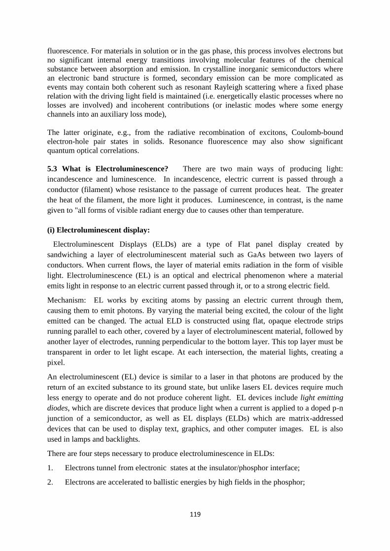
119
fluorescence. For materials in solution or in the gas phase, this process involves electrons but
no significant internal energy transitions involving molecular features of the chemical
substance between absorption and emission. In crystalline inorganic semiconductors where
an electronic band structure is formed, secondary emission can be more complicated as
events may contain both coherent such as resonant Rayleigh scattering where a fixed phase
relation with the driving light field is maintained (i.e. energetically elastic processes where no
losses are involved) and incoherent contributions (or inelastic modes where some energy
channels into an auxiliary loss mode),
The latter originate, e.g., from the radiative recombination of excitons, Coulomb-bound
electron-hole pair states in solids. Resonance fluorescence may also show significant
quantum optical correlations.
5.3 What is Electroluminescence? There are two main ways of producing light:
incandescence and luminescence. In incandescence, electric current is passed through a
conductor (filament) whose resistance to the passage of current produces heat. The greater
the heat of the filament, the more light it produces. Luminescence, in contrast, is the name
given to "all forms of visible radiant energy due to causes other than temperature.
(i) Electroluminescent display:
Electroluminescent Displays (ELDs) are a type of Flat panel display created by
sandwiching a layer of electroluminescent material such as GaAs between two layers of
conductors. When current flows, the layer of material emits radiation in the form of visible
light. Electroluminescence (EL) is an optical and electrical phenomenon where a material
emits light in response to an electric current passed through it, or to a strong electric field.
Mechanism: EL works by exciting atoms by passing an electric current through them,
causing them to emit photons. By varying the material being excited, the colour of the light
emitted can be changed. The actual ELD is constructed using flat, opaque electrode strips
running parallel to each other, covered by a layer of electroluminescent material, followed by
another layer of electrodes, running perpendicular to the bottom layer. This top layer must be
transparent in order to let light escape. At each intersection, the material lights, creating a
pixel.
An electroluminescent (EL) device is similar to a laser in that photons are produced by the
return of an excited substance to its ground state, but unlike lasers EL devices require much
less energy to operate and do not produce coherent light. EL devices include light emitting
diodes, which are discrete devices that produce light when a current is applied to a doped p-n
junction of a semiconductor, as well as EL displays (ELDs) which are matrix-addressed
devices that can be used to display text, graphics, and other computer images. EL is also
used in lamps and backlights.
There are four steps necessary to produce electroluminescence in ELDs:
1. Electrons tunnel from electronic states at the insulator/phosphor interface;
2. Electrons are accelerated to ballistic energies by high fields in the phosphor;
120
3. The energetic electrons impact-ionize the luminescent center or create electron-hole
pairs that lead to the activation of the luminescent center; and
4. The luminescent center relaxes toward the ground state and emits a photon.
All ELDs have the same basic structure. There are at least six layers to the device. The first
layer is a base plate (usually a rigid insulator like glass), the second is a conductor, the third is
an insulator, the fourth is a layer of phosphors, and the fifth is an insulator, and the sixth is
another conductor. ELDs are quite similar to capacitors except for the phosphor layer
(Fig.5.1)
Figure 5.1. Structure of an Electroluminescent Display
5.4 LED Display:
(i) What is an LED Display?
An LED display, or light emitting diode display, is a flat panel display that uses light
emitting diodes as the video display. An LED display panel can be either a small display or
part of a larger display. LED diodes are used in order to make up an LED display. LED
displays are also used in billboards and store signs. An LED panel consists of several LEDs,
whereas an LED display consists of several LED panels. LEDs used in order to make up LED
displays offer several advantages in comparison to other light emitting sources. A light
emitting diode is made up of a semiconductor chip which is surrounded by a transparent
plastic case. The plastic case allows the light to pass through it. The emission of different
colors including ultraviolet and infrared light depends on the semiconductor material which is
used in the diode.
(ii) Types of LED Displays
There are many different kinds of LED Displays.. The most common types for display type
are light bar, seven segment and dot matrix. We also carry many other different types of
121
display. Digit/Alpha/Matrix Size can range from 0.03 in to 0.40 in, with the most common
sizes being 0.2 in, 0.3 in and 0.4 in.
(iii) Applications for LED Displays:
LED displays are often found outdoors in billboards and store signs. They can also be found
in destination signs on public transportation vehicles or as part of transparent glass area. LED
panels can either be used for lighting or for general illumination, task lighting or stage
lighting. LED displays can be found in sports stadiums, public squares, train stations,
airports, highways, commercial plazas, subways, parks, shopping centers, on tall buildings
and for corporate image promotion and advertising. Due to the far viewing distances in sports
venues, the high brightness of LED displays can meet this special requirement and ensure
that viewers get clear images.
5.5 Drive circuitry
In electronics, a driver is an electrical circuit or other electronic component used to control
another circuit or component, such as a high-power transistor, liquid crystal display (LCD),
and numerous others. They are usually used to regulate current flowing through a circuit or
to control other factors such as other components, some devices in the circuit. The term is
often used, for example, for a specialized integrated circuit that controls high-power switches
in switched-mode power converters. An amplifier can also be considered a driver for
loudspeakers, or a constant voltage circuit that keeps an attached component operating within
a broad range of input voltages.
Typically the driver stage(s) of a circuit requires different characteristics to other circuit
stages. For example in a transistor power amplifier, typically the driver circuit requires
current gain, often the ability to discharge the following transistor bases rapidly, and low
output impedance to avoid or minimize distortion.
(i) Driver Circuits: Driver circuits are most commonly used to amplify signals from
controllers or microcontrollers in order to control power switches in
semiconductor devices. Driver circuits often take on additional functions which
include isolating the control circuit and the power circuit, detecting malfunctions,
storing and reporting failures to the control system, serving as a precaution against
failure, analyzing sensor signals, and creating auxiliary voltages.
(ii) Thyristor Driver Circuits: In thyristor driver circuits, appropriate control signals
are used to generate gate current pulses in order to trigger the thyristor. A
transformer often isolates the control circuit from the high voltages of the power
circuit (Fig.5.2)
(iii) Drive circuits for LED and Laser
LEDs are mostly driven by a digital signal through it can also be modulated
with an analog signal. There are various types of driver circuits for LED
modulator of which two most popular are shown in Fig.5.3 . LEDs are easy to turn
ON quickly, but are difficult to turn OFF because of the relatively long carrier life
time. In 5.3(a), resistor R2 provides the necessary current to turn ON the LED.
122
Typically R2 would be in the 40 KΩ range. This makes the turn on current ~ 100
mA peak for a +5V supply. Transistor Q1 will an impedance of a few ohms, which
provides a much larger discharge current allowing the LED to turn OFF quickly.
A disadvantage of this circuit is that it draws more current and power when the
LED is OFF than the LED is ON.
Figure 5.2. Principle of a thyristor driver circuit
A better version of the circuit is shown in Fig.5.3(b). Two additional resistors and two
capacitors have been added to the basic circuit to improve the operating speed. Capacitor C1
serves to improve the turn ON and turn OFF characteristics of the transistor itself. Resistors
R3, R4, and capacitor C2 provide overdrive when the LED is turned ON and underdrive when
the transistor is turned OFF. The overdrive and underdrive accelerates the LED transitions.
The R3C2 time constant is made approximately equal to the rise and fall time of the LED
itself when driven with a digital signal. All these tricks together can increase the operating
speed of LED and the driver circuit to about 270 Mb/s and can be pushed up to 1Gb/s.
Lasers, of course, can operate mush faster but their drive circuits are much more complex
due to compensate for variations in temperature, drive current and power supply voltage.
(a) (b)
Fig.5.3 LED drive circuits (a) Simple circuit (b) Improved version of (a)
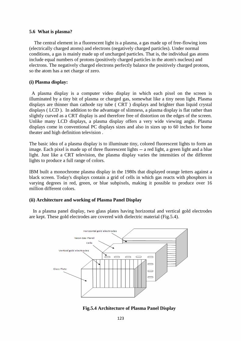
123
5.6 What is plasma?
The central element in a fluorescent light is a plasma, a gas made up of free-flowing ions
(electrically charged atoms) and electrons (negatively charged particles). Under normal
conditions, a gas is mainly made up of uncharged particles. That is, the individual gas atoms
include equal numbers of protons (positively charged particles in the atom's nucleus) and
electrons. The negatively charged electrons perfectly balance the positively charged protons,
so the atom has a net charge of zero.
(i) Plasma display:
A plasma display is a computer video display in which each pixel on the screen is
illuminated by a tiny bit of plasma or charged gas, somewhat like a tiny neon light. Plasma
displays are thinner than cathode ray tube ( CRT ) displays and brighter than liquid crystal
displays ( LCD ). In addition to the advantage of slimness, a plasma display is flat rather than
slightly curved as a CRT display is and therefore free of distortion on the edges of the screen.
Unlike many LCD displays, a plasma display offers a very wide viewing angle. Plasma
displays come in conventional PC displays sizes and also in sizes up to 60 inches for home
theater and high definition television .
The basic idea of a plasma display is to illuminate tiny, colored fluorescent lights to form an
image. Each pixel is made up of three fluorescent lights -- a red light, a green light and a blue
light. Just like a CRT television, the plasma display varies the intensities of the different
lights to produce a full range of colors.
IBM built a monochrome plasma display in the 1980s that displayed orange letters against a
black screen. Today's displays contain a grid of cells in which gas reacts with phosphors in
varying degrees in red, green, or blue subpixels, making it possible to produce over 16
million different colors.
(ii) Architecture and working of Plasma Panel Display
In a plasma panel display, two glass plates having horizontal and vertical gold electrodes
are kept. These gold electrodes are covered with dielectric material (Fig.5.4).
Fig.5.4 Architecture of Plasma Panel Display
124
In between these two glass plates there is another glass plate filled with neon gas. When
voltage is applied through the gold electrodes the neon gas is split in to independent cells and
they start to glow. By applying voltages through the gold electrodes this glow can be
controlled, thus, creating a display. No refresh is required in a Plasma panel display.
(iii) General characteristics: Plasma displays are bright (1,000 lux or higher for the
module), have a wide color gamut, and can be produced in fairly large sizes—up to 3.8
metres (150 in) diagonally. They had a very low-luminance "dark-room" black level
compared with the lighter grey of the unilluminated parts of an LCD screen at least in the
early history of the competing technologies. Power consumption varies greatly with
picture content, with bright scenes drawing significantly more power than darker ones .
The plasma that illuminates the screen can reach a temperature of at least 1200 °C (2200
°F). Typical power consumption is 400 watts for a 127 cm (50 in) screen. 200 to 310
watts for a 127 cm (50 in) display when set to cinema mode. Plasma screens are made
out of glass. This may causes glare from reflected objects in the viewing area.
(iv) Native plasma television resolutions: Fixed-pixel displays such as plasma TVs scale
the video image of each incoming signal to the native resolution of the display panel. The
most common native resolutions for plasma display panels are 853×480 (EDTV),
1,366×768 or 1,920×1,080 (HDTV). As a result, picture quality varies depending on the
performance of the video scaling processor and the upscaling and downscaling algorithms
used by each display manufacturer.
(v) Enhanced-definition plasma television: Early plasma televisions were enhanced-
definition (ED) with a native resolution of 840×480 (discontinued) or 853×480, and
down-scaled their incoming High-definition video signals to match their native display
resolution.
(vi) High-definition plasma television: Early high-definition (HD) plasma displays had a
resolution of 1024x1024 and were alternate lighting of surfaces (ALiS) panels made by
Fujitsu/Hitachi. These were interlaced displays, with non-square pixels.
Modern HDTV plasma televisions usually have a resolution of 1,024×768 found on
many 42 inch plasma screens, 1,280×768, 1,366×768 found on 50 in, 60 in, and 65 in
plasma screens, or 1,920×1,080 found in plasma screen sizes from 42 inch to 103 inch.
These displays are usually progressive displays, with square pixels, and will up-scale their
incoming standard-definition signals to match their native display resolution. 1024x768
resolution requires that 720p content be downscaled.
(vii) Contrast ratio: Contrast ratio is the difference between the brightest and darkest parts
of an image, measured in discrete steps, at any given moment. Generally, the higher the
contrast ratio, the more realistic the image is . Contrast ratios for plasma displays are
often advertised as high as 5,000,000:1. On the surface, this is a significant advantage of
plasma over most other current display technologies, a notable exception being organic
light-emitting diode.
125
(viii) Screen burn-in: Image burn-in occurs on CRTs and plasma panels when the same
picture is displayed for long periods. This causes the phosphors to overheat, losing some
of their luminosity and producing a "shadow" image that is visible with the power off.
Burn-in is especially a problem on plasma panels because they run hotter than CRTs.
Early plasma televisions were plagued by burn-in, making it impossible to use video
games or anything else that displayed static images.
Plasma displays also exhibit another image retention issue which is sometimes
confused with screen burn-in damage. In this mode, when a group of pixels are run at
high brightness (when displaying white, for example) for an extended period, a charge
build-up in the pixel structure occurs and a ghost image can be seen. However, unlike
burn-in, this charge build-up is transient and self-corrects after the image condition that
caused the effect has been removed and a long enough period has passed (with the display
either off or on).
(ix) Plasma display advantages and disadvantages:
Advantages:
(i) Capable of producing deeper blacks allowing for superior contrast ratio.
(ii) Wider viewing angles than those of LCD; images do not suffer from
degradation at less than straight ahead angles like LCDs. LCDs using IPS technology
have the widest angles, but they do not equal the range of plasma primarily due to "IPS
glow", a generally whitish haze that appears due to the nature of the IPS pixel design.
(iii) Less visible motion blur, thanks in large part to very high refresh rates and a faster
response time, contributing to superior performance when displaying content with
significant amounts of rapid motion. Superior uniformity. LCD panel backlights nearly
always produce uneven brightness levels, although this is not always noticeable. High-
end computer monitors have technologies to try to compensate for the uniformity
problem.
(iv) Unaffected by clouding from the polishing process. Some LCD panel types, like IPS,
require a polishing process that can introduce a haze usually referred to as "clouding".
(v) Less expensive for the buyer per square inch than LCD, particularly when equivalent
performance is considered.
Disadvantages:
(i) Earlier generation displays were more susceptible to screen burn-in and image
retention. Recent models have a pixel orbiter that moves the entire picture slower than is
noticeable to the human eye, which reduces the effect of burn-in but does not prevent it.
(ii) Due to the bistable nature of the colour and intensity generating method, some
people will notice that plasma displays have a shimmering or flickering effect with a
number of hues, intensities and dither patterns. Earlier generation displays (circa 2006
and prior) had phosphors that lost luminosity over time, resulting in gradual decline of
absolute image brightness. Newer models have advertised lifespans exceeding 100 000
hours, far longer than older CRTs.
(iii) Uses more electrical power, on average, than an LCD TV using an LED backlight.
Older CCFL backlights for LCD panels used quite a bit more power, and older plasma
TVs used quite a bit more power than recent models.
126
(iv) Does not work as well at high altitudes above 6,500 feet (2,000 metres] due to
pressure differential between the gases inside the screen and the air pressure at altitude. It
may cause a buzzing noise. Manufacturers rate their screens to indicate the altitude
parameters.
(v) For those who wish to listen to AM radio, or are amateur radio operators (hams) or
shortwave listeners (SWL), the radio frequency interference (RFI) from these devices can
be irritating or disabling. Plasma displays are generally heavier than LCD, and may
require more careful handling such as being kept upright.
5.7 What are liquid crystals ?: Materials in nature can be divided into different phases,
also called states of matter, depending on the mobility of the individual atoms or
molecules. The obvious states of matter are the solid, the fluid and the gaseous state. In
the solid state, intermolecular forces keep the molecules close together at a fixed position
and orientation, so the material remains in a definite shape. In the fluid state, the
molecules are still packed closely together, but they are able to move around. Hence a
fluid does not have a rigid shape, but adapts to the contours of the container that holds it.
Like a liquid a gas has no fixed shape, but it has little resistance to compression because
there is enough empty space for the molecules to move closer. Whereas a liquid placed in
a container will form a puddle at the bottom of the container, a gas will expand to fill the
container.
Apart from the three familiar states, there exist a large number of other intermediate
phases. A simple example is a gel. A gel is not quite solid, neither is it a liquid. Liquid
crystals are another important intermediate phase which exhibits features from both the
solid and the fluid state. Liquid crystals have the ordering properties of solids but they
flow like liquids. Liquid crystalline materials have been observed for over a century but
were not recognized as such until 1880s. In 1888, Friedrich Reinitzer is credited for the
first systematic description of the liquid crystal phase and reported his observations when
he prepared cholesteryl benzoate, the first liquid crystal.
The following parameters describe the liquid crystalline structure:
(i) Positional Order
(ii) Orientational Order
(iii) Bond Orientational Order
Each of these parameters describes the extent to which the liquid crystal sample is ordered.
Positional order refers to the extent to which an average molecule or group of molecules
shows translational symmetry . Orientational order, as discussed above, represents a measure
of the tendency of the molecules to align along the director on a long-range basis. Bond
Orientational Order describes a line joining the centers of nearest-neighbor molecules without
requiring a regular spacing along that line. Thus, a relatively long-range order with respect to
the line of centers but only short range positional order along that line.
Liquid crystals are composed of moderate size organic molecules which tend to be
elongated, like a cigar. At high temperatures, the molecules will be oriented arbitrarily, as
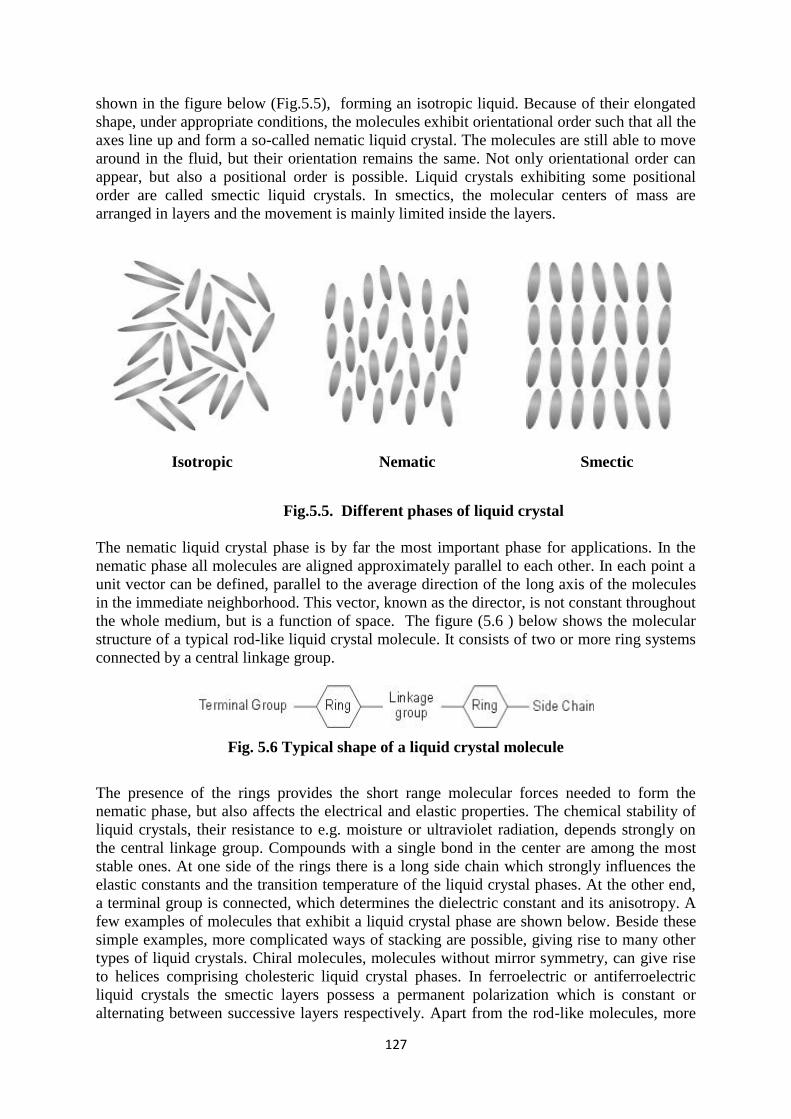
127
shown in the figure below (Fig.5.5), forming an isotropic liquid. Because of their elongated
shape, under appropriate conditions, the molecules exhibit orientational order such that all the
axes line up and form a so-called nematic liquid crystal. The molecules are still able to move
around in the fluid, but their orientation remains the same. Not only orientational order can
appear, but also a positional order is possible. Liquid crystals exhibiting some positional
order are called smectic liquid crystals. In smectics, the molecular centers of mass are
arranged in layers and the movement is mainly limited inside the layers.
Isotropic Nematic Smectic
Fig.5.5. Different phases of liquid crystal
The nematic liquid crystal phase is by far the most important phase for applications. In the
nematic phase all molecules are aligned approximately parallel to each other. In each point a
unit vector can be defined, parallel to the average direction of the long axis of the molecules
in the immediate neighborhood. This vector, known as the director, is not constant throughout
the whole medium, but is a function of space. The figure (5.6 ) below shows the molecular
structure of a typical rod-like liquid crystal molecule. It consists of two or more ring systems
connected by a central linkage group.
Fig. 5.6 Typical shape of a liquid crystal molecule
The presence of the rings provides the short range molecular forces needed to form the
nematic phase, but also affects the electrical and elastic properties. The chemical stability of
liquid crystals, their resistance to e.g. moisture or ultraviolet radiation, depends strongly on
the central linkage group. Compounds with a single bond in the center are among the most
stable ones. At one side of the rings there is a long side chain which strongly influences the
elastic constants and the transition temperature of the liquid crystal phases. At the other end,
a terminal group is connected, which determines the dielectric constant and its anisotropy. A
few examples of molecules that exhibit a liquid crystal phase are shown below. Beside these
simple examples, more complicated ways of stacking are possible, giving rise to many other
types of liquid crystals. Chiral molecules, molecules without mirror symmetry, can give rise
to helices comprising cholesteric liquid crystal phases. In ferroelectric or antiferroelectric
liquid crystals the smectic layers possess a permanent polarization which is constant or
alternating between successive layers respectively. Apart from the rod-like molecules, more
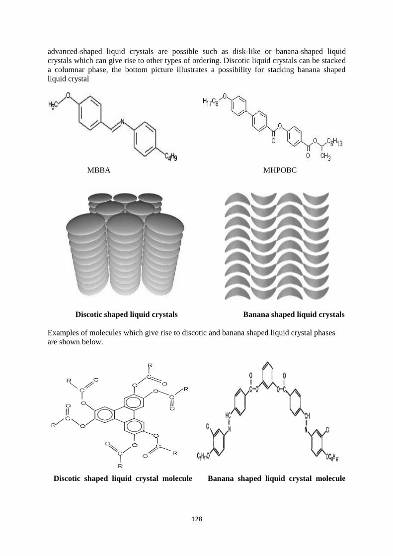
128
advanced-shaped liquid crystals are possible such as disk-like or banana-shaped liquid
crystals which can give rise to other types of ordering. Discotic liquid crystals can be stacked
a columnar phase, the bottom picture illustrates a possibility for stacking banana shaped
liquid crystal
MBBA MHPOBC
Discotic shaped liquid crystals Banana shaped liquid crystals
Examples of molecules which give rise to discotic and banana shaped liquid crystal phases
are shown below.
Discotic shaped liquid crystal molecule Banana shaped liquid crystal molecule
129
One type of liquid crystal molecule can exhibit many different liquid crystal phases. The
phase in which a pure liquid crystal (with only one type of molecule) exists depends on the
temperature. Pure liquid crystals, or mixtures of them, in which the phase is controlled by
temperature are called thermotropic liquid crystals. The Brownian motion of the molecules
increases with the temperature, reducing the order in the material. At high temperature,
orientational order is lost and the material changes to the isotropic phase. When decreasing
the temperature, the material changes to the nematic phase. The temperature at which the
phase transition occurs, is specific for each material and is called the nematic-isotropic
transition temperature or clearing point. By further lowering the temperature, the phase can
change to the smectic A phase, the smectic C and finally to the solid state. Each of the phase
transitions occurs at a specific temperature, but depending on the material additional phases
can appear or some can be missing.
Beside the thermotropic liquid crystals, a different class of liquid crystals is called lyotropic.
These are mixtures of rod-like molecules in an isotropic solvent and the concentration of the
solution is primarily responsible for the occurring phase. Lyotropic liquid crystals are mainly
of interest in biological applications and exhibit a considerable number of different phases. In
our research, only thermotropic liquid crystal are examined. The ordering of the liquid crystal
molecules may seem strange, but in our daily environment similar arrangements are common.
(i) Chemical Properties of Liquid Crystals
Liquid crystals can be classified into two main categories: thermotropic liquid crystals,
and lyotropic liquid crystals. These two types of liquid crystals are distinguished by the
mechanisms that drive their self-organization, but they are also similar in many ways.
Thermotropic transactions occur in most liquid crystals, and they are defined by the fact that
the transitions to the liquid crystalline state are induced thermally. That is, one can arrive at
the liquid crystalline state by raising the temperature of a solid and/or lowering the
temperature of a liquid. Thermotropic liquid crystals can be classified into two types:
enantiotropic liquid crystals, which can be changed into the liquid crystal state from either
lowering the temperature of a liquid or raising of the temperature of a solid, and monotropic
liquid crystals, which can only be changed into the liquid crystal state from either an increase
in the temperature of a solid or a decrease in the temperature of a liquid, but not both. In
general, thermotropic mesophases occur because of anisotropic dispersion forces between the
molecules and because of packing interactions. In contrast to thermotropic mesophases,
lyotropic liquid crystal transitions occur with the influence of solvents, not by a change in
temperature. Lyotropic mesophases occur as a result of solvent-induced aggregation of the
constituent mesogens into micellar structures. Lyotropic mesogens are typically
amphiphilic , meaning that they are composed of both lyophilic (solvent- attracting) and
lyophobic (solvent-repelling) parts. This causes them to form into micellar structures in the
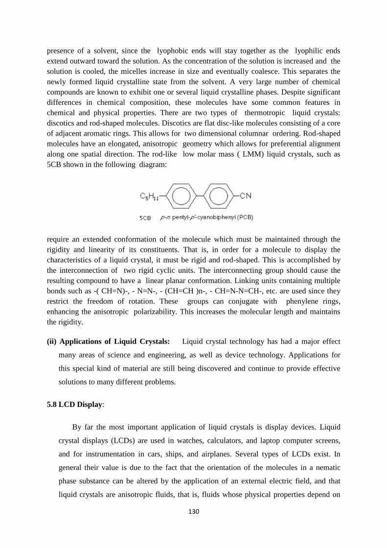
130
presence of a solvent, since the lyophobic ends will stay together as the lyophilic ends
extend outward toward the solution. As the concentration of the solution is increased and the
solution is cooled, the micelles increase in size and eventually coalesce. This separates the
newly formed liquid crystalline state from the solvent. A very large number of chemical
compounds are known to exhibit one or several liquid crystalline phases. Despite significant
differences in chemical composition, these molecules have some common features in
chemical and physical properties. There are two types of thermotropic liquid crystals:
discotics and rod-shaped molecules. Discotics are flat disc-like molecules consisting of a core
of adjacent aromatic rings. This allows for two dimensional columnar ordering. Rod-shaped
molecules have an elongated, anisotropic geometry which allows for preferential alignment
along one spatial direction. The rod-like low molar mass ( LMM) liquid crystals, such as
5CB shown in the following diagram:
require an extended conformation of the molecule which must be maintained through the
rigidity and linearity of its constituents. That is, in order for a molecule to display the
characteristics of a liquid crystal, it must be rigid and rod-shaped. This is accomplished by
the interconnection of two rigid cyclic units. The interconnecting group should cause the
resulting compound to have a linear planar conformation. Linking units containing multiple
bonds such as -( CH=N)-, - N=N-, - (CH=CH )n-, - CH=N-N=CH-, etc. are used since they
restrict the freedom of rotation. These groups can conjugate with phenylene rings,
enhancing the anisotropic polarizability. This increases the molecular length and maintains
the rigidity.
(ii) Applications of Liquid Crystals: Liquid crystal technology has had a major effect
many areas of science and engineering, as well as device technology. Applications for
this special kind of material are still being discovered and continue to provide effective
solutions to many different problems.
5.8 LCD Display:
By far the most important application of liquid crystals is display devices. Liquid
crystal displays (LCDs) are used in watches, calculators, and laptop computer screens,
and for instrumentation in cars, ships, and airplanes. Several types of LCDs exist. In
general their value is due to the fact that the orientation of the molecules in a nematic
phase substance can be altered by the application of an external electric field, and that
liquid crystals are anisotropic fluids, that is, fluids whose physical properties depend on
131
the direction of measurement. It is not pure liquid crystalline compounds that are used in
LCDs, but liquid crystal mixtures having optimized properties.
The simplest LCDs that display letters and numbers have no internal light source. They
make use of surrounding light, which is selectively reflected or absorbed. An LCD is
analogous to a mirror that is made nonreflective at distinct places on its surface for a
certain period. The main advantage of an LCD is low energy consumption. More
advanced LCDs need back light, color filters, and advanced electronics to display
complex figures. The best-known LCD is the so-called twisted nematic display.
(i) Liquid Crystal Thermometers: As demonstrated earlier, chiral nematic (cholesteric)
liquid crystals reflect light with a wavelength equal to the pitch. Because the pitch is
dependent upon temperature, the color reflected also is dependent upon temperature.
Liquid crystals make it possible to accurately gauge temperature just by looking at the
color of the thermometer. By mixing different compounds, a device for practically any
temperature range can be built. The "mood ring", a popular novelty a few years ago, took
advantage of the unique ability of the chiral nematic liquid crystal. More important and
practical applications have been developed in such diverse areas as medicine and
electronics. Special liquid crystal devices can be attached to the skin to show a "map" of
temperatures. This is useful because often physical problems, such as tumors, have a
different temperature than the surrounding tissue. Liquid crystal temperature sensors can
also be used to find bad connections on a circuit board by detecting the characteristic
higher temperature.
((ii) Optical Imaging recording: In this technology, a liquid crystal cell is placed between
two layers of photoconductor. Light is applied to the photoconductor, which increases
the material's conductivity. This causes an electric field to develop in the liquid crystal
corresponding to the intensity of the light. The electric pattern can be transmitted by an
electrode, which enables the image to be recorded. This technology is still being
developed and is one of the most promising areas of liquid crystal research.
(iii) Other Liquid Crystal Applications: Liquid crystals have a multitude of other uses.
They are used for nondestructive mechanical testing of materials under stress. This
technique is also used for the visualization of RF (radio frequency) waves in
waveguides. They are used in medical applications where, for example, transient pressure
132
transmitted by a walking foot on the ground is measured. Low molar mass (LMM) liquid
crystals have applications including erasable optical disks, full color "electronic slides"
for computer-aided drawing (CAD), and light modulators for color electronic imaging.
As new properties and types of liquid crystals are investigated and researched, these
materials are sure to gain increasing importance in industrial and scientific applications.
5.9 LED Numeric Displays:
Numeric LED displays, sometimes referred to as 7 segment displays due to the layout
of the display allowing to show only numbers, are an eye catching way to display numeric
information. This type of display is used for applications such as LED Fuel Price Signs,
LED Time & Temperature displays and LED Countdown Clocks where displaying highly
visible prices and other numeric information is vital.
(i) Concept and visual structure: The individual segments of a seven-segment display
16x8-grid showing the 128 states of a seven-segment display. The common segment
displays shown side by side: 7-segment, 9-segment, 14-segment and 16-segment displays.
The seven elements of the display can be lit in different combinations to represent the
arabic numerals. Often the seven segments are arranged in an oblique (slanted)
arrangement, which aids readability. In most applications, the seven segments are of
nearly uniform shape and size (usually elongated hexagons, though trapezoids and
rectangles can also be used), though in the case of adding machines, the vertical segments
are longer and more oddly shaped at the ends in an effort to further enhance readability.
The numerals 6 and 9 may be represented by two different glyphs on seven-segment
displays, with or without a 'tail'. The seven segments are arranged as a rectangle of two
vertical segments on each side with one horizontal segment on the top, middle, and
bottom. Additionally, the seventh segment bisects the rectangle horizontally. There are
also fourteen-segment displays and sixteen-segment displays (for full alphanumerics);
however, these have mostly been replaced by dot matrix displays. The segments of a 7-
segment display are referred to by the letters A to G, where the optional decimal point (an
"eighth segment", referred to as DP) is used for the display of non-integer numbers.
(ii) Implementations: Seven-segment displays may use a liquid crystal display (LCD), a
light-emitting diode (LED) for each segment, or other light-generating or controlling
techniques such as cold cathode gas discharge, vacuum fluorescent, incandescent
133
filaments, and others. For gasoline price totems and other large signs, vane displays made
up of electromagnetically flipped light-reflecting segments (or "vanes") are still
commonly used. An alternative to the 7-segment display in the 1950s through the 1970s
was the cold-cathode, neon-lamp-like nixie tube. Starting in 1970, RCA sold a display
device known as the Numitron that used incandescent filaments arranged into a seven-
segment display. In a simple LED package, typically all of the cathodes (negative
terminals) or all of the anodes (positive terminals) of the segment LEDs are connected
and brought out to a common pin; this is referred to as a "common cathode" or "common
anode" device. Hence a 7 segment plus decimal point package will only require nine pins,
though commercial products typically contain more pins, and/or spaces where pins would
go, in order to match standard IC sockets. Integrated displays also exist, with single or
multiple digits. Some of these integrated displays incorporate their own internal decoder,
though most do not: each individual LED is brought out to a connecting pin as described.
A multiplexed 4-digit, seven-segment display with only 12 pins Multiple-digit LED
displays as used in pocket calculators and similar devices used multiplexed displays to
reduce the number of I/O pins required to control the display. For example, all the anodes
of the A segments of each digit position would be connected together and to a driver
circuit pin, while the cathodes of all segments for each digit would be connected. To
operate any particular segment of any digit, the controlling integrated circuit would turn
on the cathode driver for the selected digit, and the anode drivers for the desired
segments; then after a short blanking interval the next digit would be selected and new
segments lit, in a sequential fashion. In this manner an eight digit display with seven
segments and a decimal point would require only 8 cathode drivers and 8 anode drivers,
instead of sixty-four drivers and IC pins. Often in pocket calculators the digit drive lines
would be used to scan the keyboard as well, providing further savings; however, pressing
multiple keys at once would produce odd results on the multiplexed display. A single byte
can encode the full state of a 7-segment-display. The most popular bit encodings are
gfedcba and abcdefg, where each letter represents a particular segment in the display. In
the gfedcba representation, a byte value of 0x06 would (in a common-anode circuit) turn
on segments 'c' and 'b', which would display a '1'.
(iv) Displaying letters:: Hexadecimal digits can be displayed on seven-segment
displays. A combination of uppercase and lowercase letters is used for A–F; this is
done to obtain a unique, unambiguous shape for each hexadecimal digit
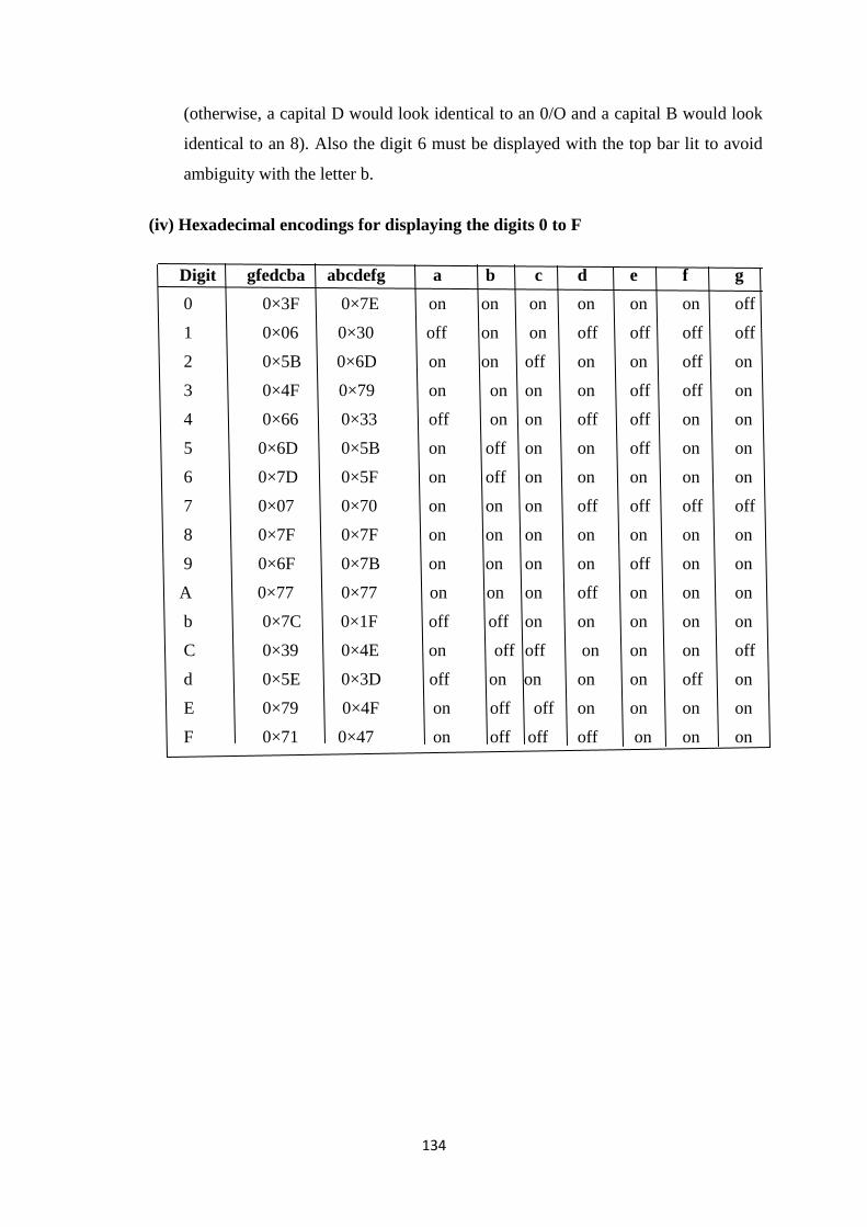
134
(otherwise, a capital D would look identical to an 0/O and a capital B would look
identical to an 8). Also the digit 6 must be displayed with the top bar lit to avoid
ambiguity with the letter b.
(iv) Hexadecimal encodings for displaying the digits 0 to F
Digit gfedcba abcdefg a b c d e f g
0 0×3F 0×7E on on on on on on off
1 0×06 0×30 off on on off off off off
2 0×5B 0×6D on on off on on off on
3 0×4F 0×79 on on on on off off on
4 0×66 0×33 off on on off off on on
5 0×6D 0×5B on off on on off on on
6 0×7D 0×5F on off on on on on on
7 0×07 0×70 on on on off off off off
8 0×7F 0×7F on on on on on on on
9 0×6F 0×7B on on on on off on on
A 0×77 0×77 on on on off on on on
b 0×7C 0×1F off off on on on on on
C 0×39 0×4E on off off on on on off
d 0×5E 0×3D off on on on on off on
E 0×79 0×4F on off off on on on on
F 0×71 0×47 on off off off on on on
MANONMANIAM SUNDARANAR UNIVERSITY
DIRECTORATE OF DISTANCE & CONTINUING EDUCATION
TIRUNELVELI 627012, TAMIL NADU
M.SC. PHYSICS - II YEAR
DKP23 - LASERS AND OPTO ELECTRONICS
(From the academic year 2016-17)
Most Student friendly University - Strive to Study and Learn to Excel
For more information visit: http://www.msuniv.ac.in