Embed Size (px)
Citation preview

Unit– III
Transistors
Index
Introduction
3.1 PNP and NPN transistor (working principle)
3.2 Transistor as switch
3.3 FET, working of PMOS and NMOS
3.4 Working of CMOS Logic Family
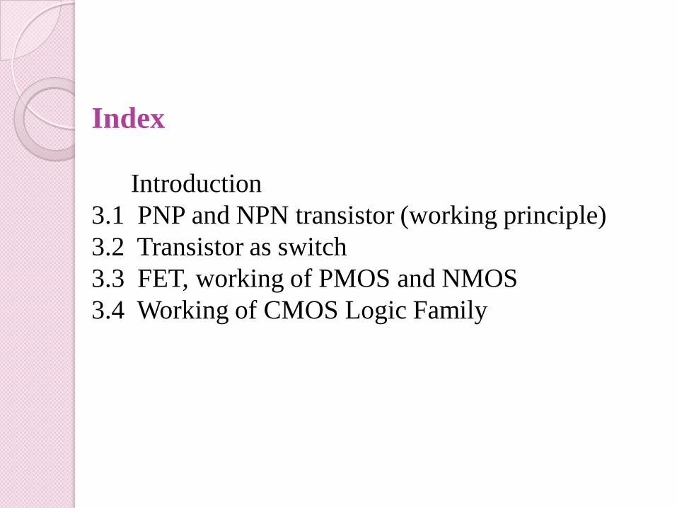
Inroduction
Transistor symbol and its construction:


Define:
A transistor consists of two p-n junction
formed by sandwiching either p-type or n-type
semiconductor between a pair of opposite types.
Types
When N-type semiconductor is kept between
two p-type semiconductor, it is known as the PNP
transistor.
When P-type semiconductor is kept between
two N-type semiconductor, it is known as the NPN
transistor.
• If semiconductor material used is germanium or
silicon , it is called the germanium or silicon
transistor accordingly.
• One lead is taken out from the each layer. These are
respectively called emitter, base and collector.
• In figure arrow is shown on the emitter lead which
shows the direction of current through the transistor.
• The base is thin and lightly doped.
• The emitter is heavily doped and its size is larger than
the base.
• Size of the collector is larger than emitter as the
collector has to dissipate the heat.

Biasing of transistor : (1) PNP transistor & (2) NPN
transistor.

BJT Current & Voltage - Equations
B
CE
IE IC
IB
-
+
VBE VBC
+
-
+- VCE
B
CE
IE IC
IB-
+
VEB VCB
+
-
+ -VEC
NPN
IE = IB + IC
VCE = -VBC + VBE
PNP
IE = IB + IC
VEC = VEB - VCB
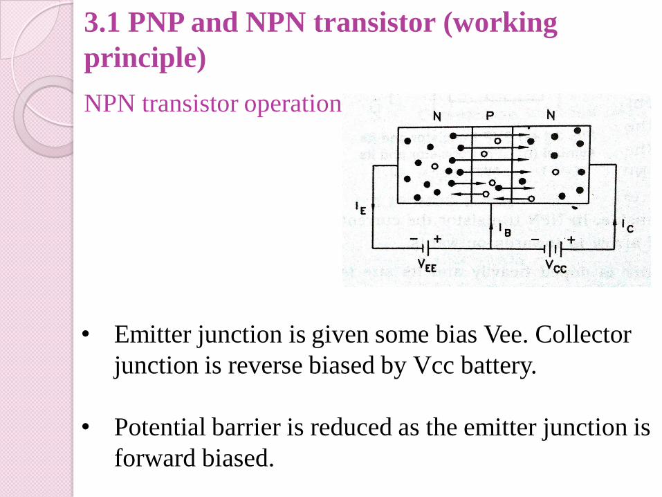
NPN transistor operation
3.1 PNP and NPN transistor (working
principle)
• Emitter junction is given some bias Vee. Collector
junction is reverse biased by Vcc battery.
• Potential barrier is reduced as the emitter junction is
forward biased.
• Electron from emitter cross the junction and go
to the base.
• Holes from the base cross the junction and go to
emitter. So current Ie flows due to the flow of
majority charge carries. It is called the emitter
current.
• In this current due to the hole movement is very
less as the base is thin and lightly doped. Current
due to the flow of electrons is much more.

• Electrons injected from emitter come to the base
but as the base is thin and lightly doped, very
small number of electrons combine with the holes
in base.
• Most of the electrons are collected by the
collector.

PNP transistor operation
• Emitter base junction is forward biased and the
collector base junction is reverse biased.
• As the emitter junction is forward biased, the
barrier potential is reduced.
• Majority charge carriers (hole) in emitter go
towards the base (Electrons) go towards the emitter.

• Very small number of holes injected from the
emitter to the base combine with the electrons in
the base and most of the holes are collected by the
collector.
• The emitter current Ie is available due to the flow of
the majority charge carriers.
• Since the collector junction is reverse biased,
majority charge carrier ( electrons) in collector go to
the base and majority charge carrier in base (holes)
go to the collector.
• Thus this leakage current flows from base to
collector and is denoted by Icbo.
• This current is less than the movement of holes in
emitter and electron in base.
• Difference between these two current is known as
the base current Ib.
If we neglect the leakage current ,
Ie = Ib + Ic

Three configuration of transistor:
1.CE
2.CB
3.CC
• Any two port network there are two input and two
output. So there are four terminals.
• Transistor has three terminals. So when it is
connected in the circuit one terminal should be
made common to the input and output.
• Common terminal is connected to the ground. Any
one from the emitter, base or collector can be made
common. So three types of configuration are
possible.

Common-Base (CB) configuration
Common-Emitter (CE) configuration

Common-Collector (CC) configuration

Amplifier:
A transistor raises the strength of weak signal and
thus acts as an amplifier.
Amplifier is device which converts the weak signal
to strong signal.

Common Emitter amplifier:
The proper flow of zero signal collector current and
the maintenance of proper collector emitter voltage the
passage of signal is known as biasing.

• R1 and R2 are the voltage divider type bias
registers.
• Rc is the resistance in the collector circuit
• Cc1 is the input coupling capacitor which
couples the input signal to the base .
• Cc2 is another coupling capacitor which couples
the collector to load.
• Re is the resistor connected in the emitter circuit
which is used for bias stabilization.
• Gain reduces due to the voltage drop in this
resistor.
• To prevent this, a capacitor Ce is connected
across Re, So the emitter is a.c. wise connected
to ground.

• There is drop of a.c. signal across the emitter
resistor and there is no reduction in gain.
• This capacitor Ce is called the bypass capacitor.
Working
• Base current increases when the input signal
increases in positive direction.so the collector
current increases, voltage drop across Rc
increases.
• So the output voltage Vce reduces and when the
input voltage becomes negative, the base current
reduces which reduces the collector current so the
voltage drop across Rc decreases and the output
voltage increases.
• When the input voltage goes to the positive peak,
the output voltage goes to negative peak.
• Thus there is phase difference of 180
between the input and output voltages.
• Change in the output voltage is much more than the
change in the input voltage.

Parameters
1.) Voltage gain
Voltage gain Av = ∆Vo / ∆Vi
2.) Current gain
Current gain Ai = ∆Io / ∆Ii
3.) Power gain
Power gain Ap = Output power / Input power
= Voltage gain *Current gain
Ap = Av * Ai

Transistor as switch:
3.2 Transistor as switch
• If the base of an NPN transistor is given positive
voltage as shown in fig.(a).
• The emitter base junction is forward biased.
If the bias is sufficient maximum collector
current flows and transistor goes into
saturation.
• Almost all Vcc voltage is dropped in the
collector resistor Rc and the voltage drop Vce
across the transistor become very less (almost
zero).
• In this situation it is said that the transistor has
become ON.

• But as shown in fig.(b) if the base is connected to
ground or the base is given negative voltage the
base current does not flow. So the collector current
also become zero.
• So lcRc drop becomes negligible and most of the
Vcc supply dropped in the transistor.
• In this condition it is said that the transistor has
become OFF.


Cut- off : The points where the load line intersects the
Ib = 0 curve is known as cut off.
• At this point Ib = 0 and only small collector current
exists.
• At the cut-off, the base emitter junction no longer
remains forward biased and normal transistor action
is lost.
• The collector emitter voltage is nearly equal to
Vcc. i.e. Vce = Vcc.

Saturation : The point where the load line intersects the
Ib = Ib(sat) curve is called saturation.
• At this point ,the base current is maximum and so is
the collector current
• At saturation , collector base junction no longer
remains reversed biased and normal transistor action
is lost.
Ic(sat) = Vcc / Rc
• If base current is greater than Ib(sat), then collector
current cannot increase because collector base
junction is no longer reverse biased.

Active region: The region between cut-off and
saturation is known as active region.
• In the active region, collector base junction remains
reverse biased and emitter base junction remains
forward biased.
• The transistor will function normally in this region.
Applications of transistor:
• As small signal amplifier.
• In power amplifier.
• In oscillator
• In multivibrator
• In digital & analog IC
• As electronic switch
FET is semiconductor device which controls the
current.
It is uni polar device. i.e. operation depends on
only one type of charge carriers (hole or electron)
FET are mainly two types.
1.) Junction FET(JFET)
2.) Insulated gate FET (IGFT or MOSFET)
3.3 FET, working of PMOS and NMOS

Types of Field Effect Transistors
(The Classification)
JFET
MOSFET (IGFET)
n-Channel JFET
p-Channel JFET
n-Channel EMOSFET
p-Channel EMOSFET
Enhancement MOSFET
Depletion MOSFET
n-Channel DMOSFET
p-Channel DMOSFET
FET


Construction and working of FET:
(N-channel JFET)

• In this block of N type semiconductor is taken. This
is called N channel.
• There are two region of P type semiconductor on
each side of the channel.
• The P type region are joined together.
• Three terminal are taken out :
Source(S)
Drain (D)
Gate(G)

• When no supply voltage is given to the gate terminal
and the drain terminal is given positive voltage with
respect to (W.R.T.) the source terminal ,Id drain
current flows as shown in fig.
• When gate is given some negative bias w.r.t. source
(Positive supply to source and negative to gate).
• Some depletion region is formed and as the channel
is lightly doped compared to gate, the depth of the
depletion region is more in channel compared to the
gate.
• As there is absence of charge carriers in the depletion
region, it works as the insulator.

• Due to this drain current reduces.
• When negative bias is increased , depletion region
increases and drain current decreases.
• When depletion region in channel join each other,
drain current becomes zero.

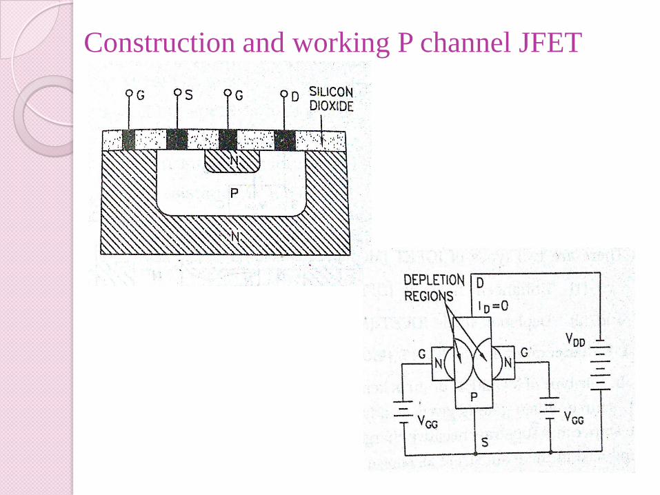
Construction and working P channel JFET
• In P-channel FET, channel of P type
semiconductor is taken and two gates of N type
are formed.
• Drain is given negative voltage w.r.t. source
whereas the gate is given reverse bias means the
gate is given positive voltage w.r.t. source.
• Construction of P channel JFET is shown in fig.
• It is similar to that of N channel JFET , but in place
of P type , N type semiconductor is kept .

• When gate is given reverse biased depletion region
is formed and the resistance of the channel
increases.
• When the value of Vgs in increased, the depletion
region increases deep further. the resistance
increases and drain current decreases.
• When Vgs is kept zero and when drain is given
negative voltage Vdd with respect to source, drain
current Id flows due to the holes in the P type
channel .
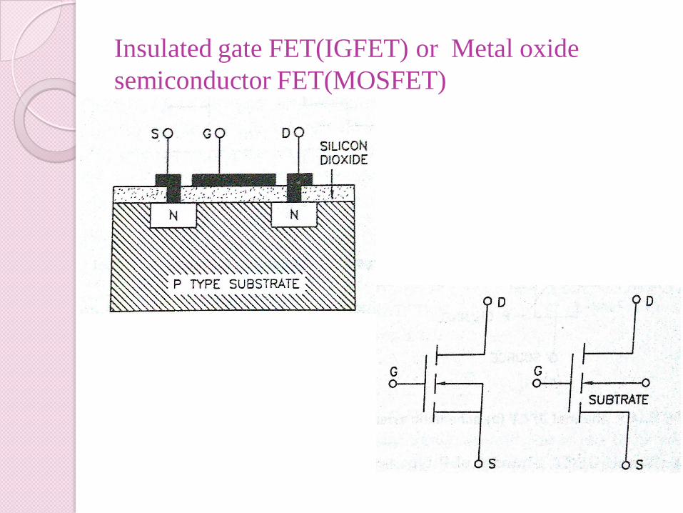
Insulated gate FET(IGFET) or Metal oxide
semiconductor FET(MOSFET)

• Two blocks of N type material are diffused in P
type semiconductor as shown in fig.
• Upper layer is coated with silicon dioxide which is
insulating material.
• Through this one lead is taken out from one N type
block and another lead is taken out from another N
type block.
• One is the drain and another is the source terminal.
• Metal coating is done on silicon dioxide over the P
type material and from that the gate lead is taken out.

• As the gate insulated from the channel in MOSFET,
its input resistance is very high (1015Ω)
• There are two types of IGFET (MOSFET)
(1) Enhancement mode IGFET
(2) Depletion mode IGFEET

Enhancement mode IGFET(MOSFET)
• In this type of MOSFET, drain is kept positive w.r.t.
source.
• When gate is given positive voltage w.r.t. source and
substrate negative charge carriers are induced in the P
substrate as shown in fig.
• As the gate potential is increased , number of induced
electrons is increased.
• These electrons are the minority charge carriers of P
type material. Due to the positive voltage on the plate
of gate, these electrons are attracted towards the plate.

• But there is insulating layer of silicon dioxide,
the electrons gather below this layer
• These electrons are between two N type blocks.
• It works as N channel and the drain current flows.
• Value of this drain current depends upon the value of
Vgs.
• The drain current increases with the increase value of
Vgs.
• Thus, the conductivity of the channel increases
enhanced. So this type of MOSFET is called
enhancement mode MOSFET or enhancement mode
IGFET.
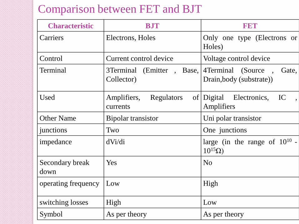
Characteristic BJT FET
Carriers Electrons, Holes Only one type (Electrons or
Holes)
Control Current control device Voltage control device
Terminal 3Terminal (Emitter , Base,
Collector)
4Terminal (Source , Gate,
Drain,body (substrate))
Used Amplifiers, Regulators of
currents
Digital Electronics, IC ,
Amplifiers
Other Name Bipolar transistor Uni polar transistor
junctions Two One junctions
impedance dVi/di large (in the range of 1010 -
1015Ω)
Secondary break
down
Yes No
operating frequency Low High
switching losses High Low
Symbol As per theory As per theory
Comparison between FET and BJT
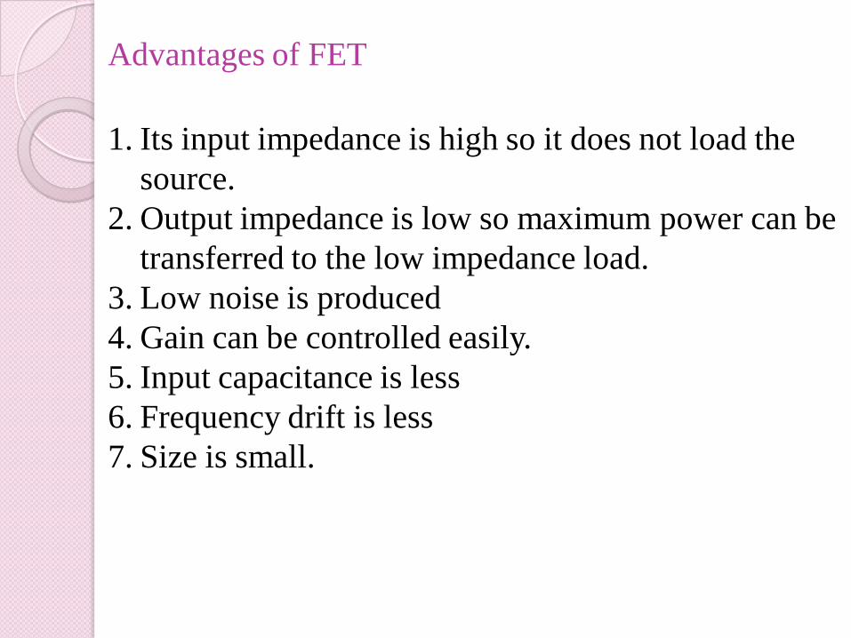
Advantages of FET
1. Its input impedance is high so it does not load the
source.
2. Output impedance is low so maximum power can be
transferred to the low impedance load.
3. Low noise is produced
4. Gain can be controlled easily.
5. Input capacitance is less
6. Frequency drift is less
7. Size is small.
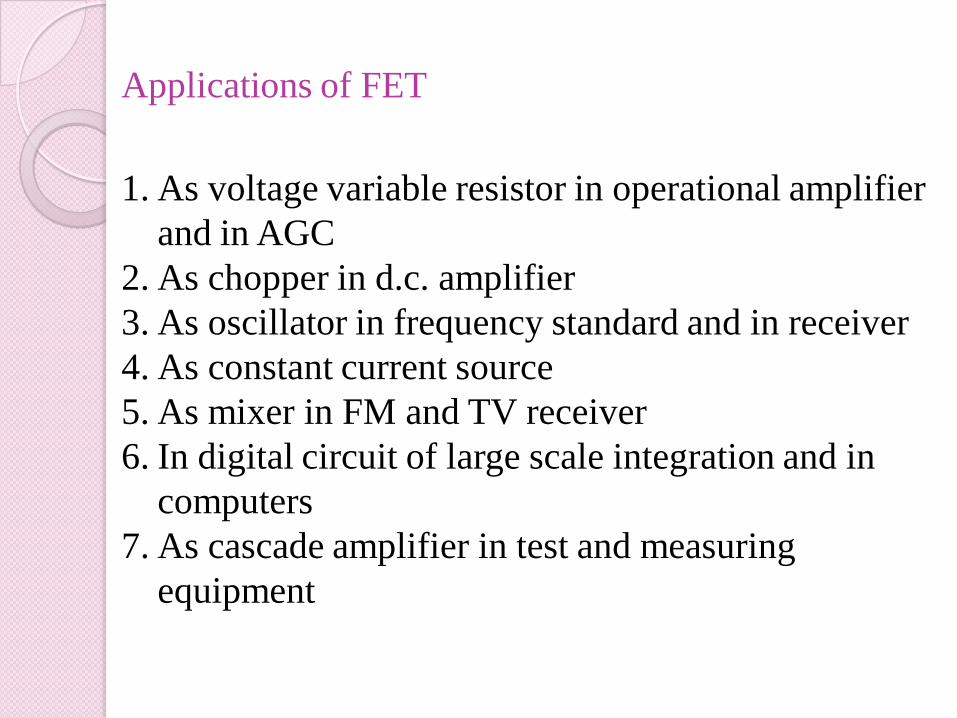
Applications of FET
1. As voltage variable resistor in operational amplifier
and in AGC
2. As chopper in d.c. amplifier
3. As oscillator in frequency standard and in receiver
4. As constant current source
5. As mixer in FM and TV receiver
6. In digital circuit of large scale integration and in
computers
7. As cascade amplifier in test and measuring
equipment

MOS family
• MOS logic has become popular due to its higher
density and low power dissipation.
• MOSFET is used in digital circuit.
• There are three types of MOS family.
1.) PMOS
2.) NMOS
3.) CMOS

PMOS
• In this P type channel enhancement mode type
MOSFET is used.
• There are three terminal, which are known as drain,
source and gate.
• Majority charge carriers enter through the source
terminal and through the drain terminal the charge
carriers go out.
• In symbol the line between the source
and drain is dotted which shows that
there is no conductive channel between
these two electrode.

NMOS
• In this N type channel is used. Majority charge
carriers are electrons.
• Symbol of NMOS is similar to PMOS. Only
direction of arrow is opposite. In this drain is given
positive voltage w.r.t. source.
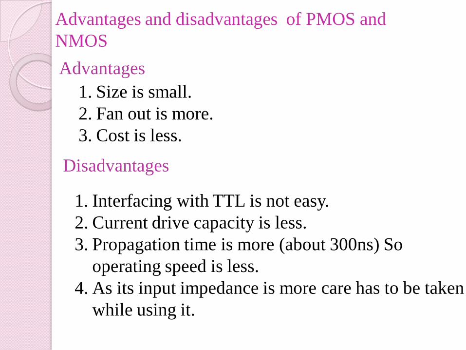
Advantages and disadvantages of PMOS and
NMOS
1. Size is small.
2. Fan out is more.
3. Cost is less.
Advantages
Disadvantages
1. Interfacing with TTL is not easy.
2. Current drive capacity is less.
3. Propagation time is more (about 300ns) So
operating speed is less.
4. As its input impedance is more care has to be taken
while using it.
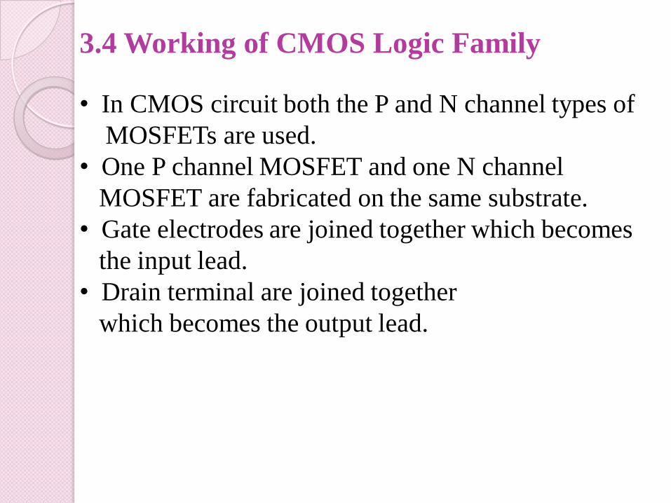
3.4 Working of CMOS Logic Family
• In CMOS circuit both the P and N channel types of
MOSFETs are used.
• One P channel MOSFET and one N channel
MOSFET are fabricated on the same substrate.
• Gate electrodes are joined together which becomes
the input lead.
• Drain terminal are joined together
which becomes the output lead.

• P channel MOSFET conducts when gate voltage is
negative w.r.t. the source voltage whereas N channel
MOSFET conducts when gate voltage is positive
w.r.t. the source voltage.
• Both become off when the gate voltage is 0.
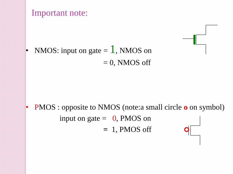
• NMOS: input on gate = 1, NMOS on
= 0, NMOS off
• PMOS : opposite to NMOS (note:a small circle o on symbol)
input on gate = 0, PMOS on
= 1, PMOS off
Important note:
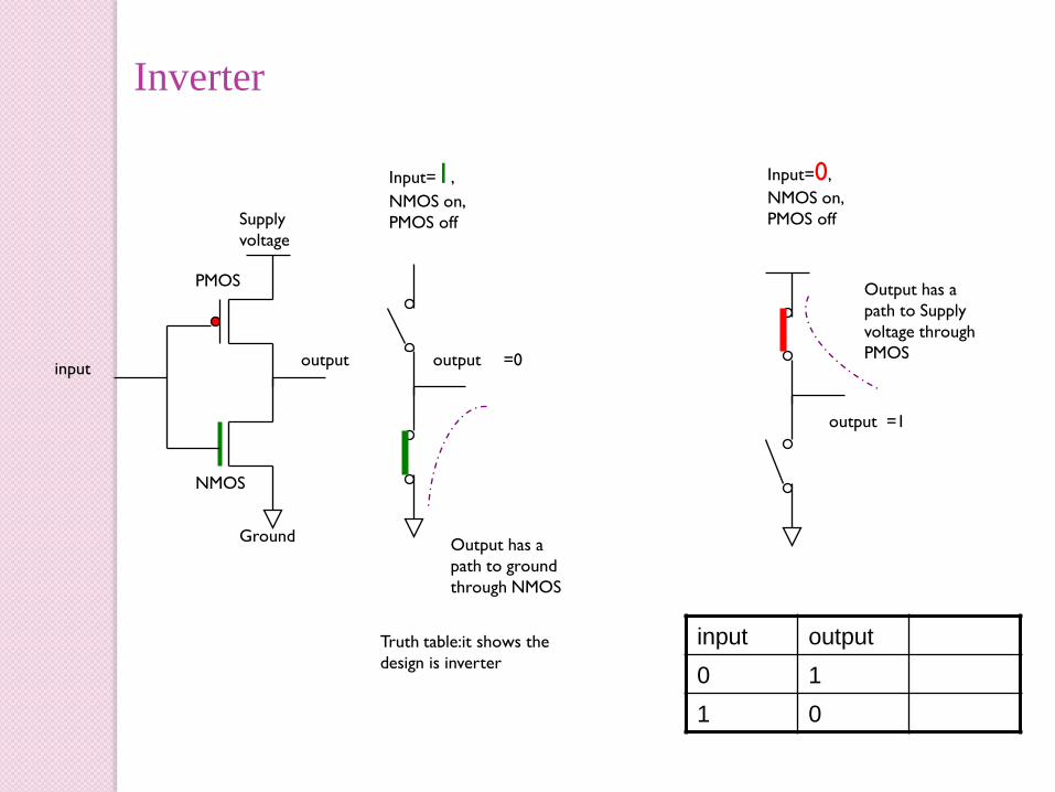
Inverter 反相器
input
PMOS
Input=1,
NMOS on,
PMOS off
output =0
Ground
Supply
voltage
Output has a
path to ground
through NMOS
output
NMOS
Input=0,
NMOS on,
PMOS off
output =1
Output has a
path to Supply
voltage through
PMOS
input output
0 1
1 0
Truth table:it shows the
design is inverter
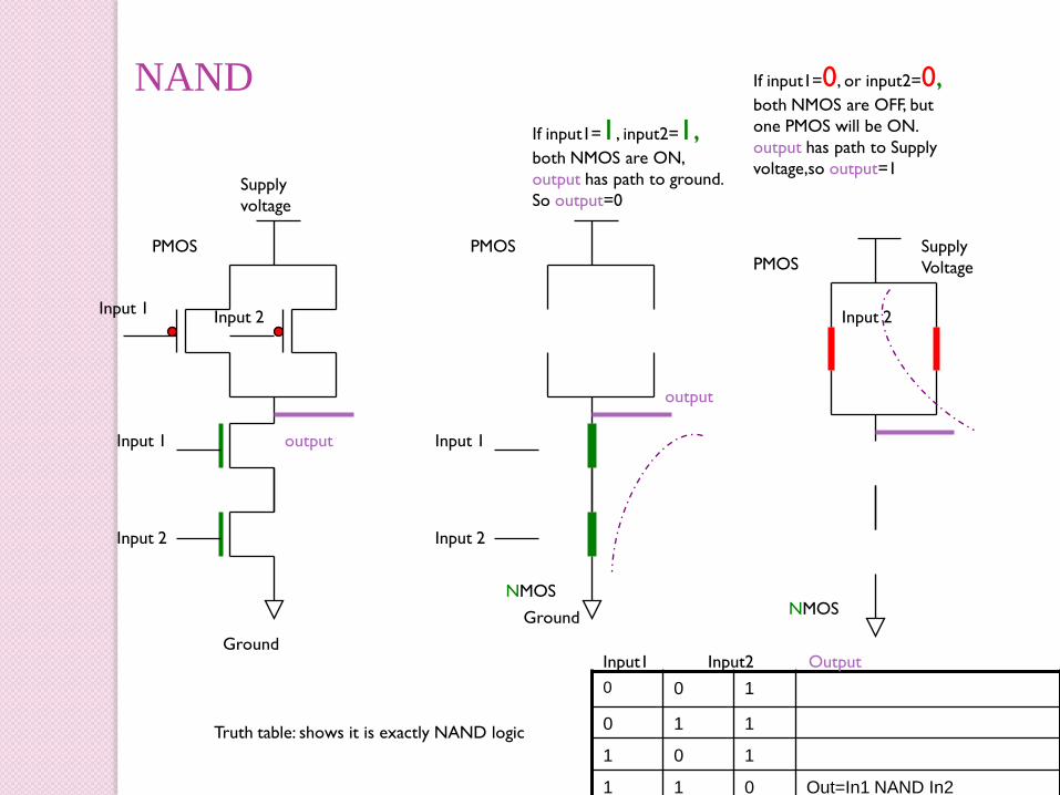
NAND 与非门
Ground
PMOS
Supply
voltage
Input 1
Input 2
Input 1Input 2
NMOS
PMOS
Input 1
Input 2
If input1=1, input2=1, both NMOS are ON,
output has path to ground.
So output=0
output
output
If input1=0, or input2=0, both NMOS are OFF, but
one PMOS will be ON.
output has path to Supply
voltage,so output=1
NMOS
PMOS
Input 2
Ground
Supply
Voltage
0 0 1
0 1 1
1 0 1
1 1 0 Out=In1 NAND In2
Input1 Input2 Output
Truth table: shows it is exactly NAND logic

Dual design: 举NOR或例门:NMOS 并联时,PMOS对偶的部分串联DDual Design: PMOS in serial, NMOS in Parallel;
Ground
PMOS
Supply
voltage
Input 1
Input 2
Input 1Input 2
output
If input1=0, or input2=0, both NMOS are OFF, but
one PMOS will be ON.
output has path to Supply
voltage,so output=1
NMOS
PMOSSupply
Voltage
0 0 1
0 1 0
1 0 0
1 1 0 Out=In1 NOR In2
Input1 Input2 Output
Truth table: shows it is exactly NOR logic

Advantages and disadvantages of CMOS over TTL
ICs.
Advantages
1. Its internal circuit is simple.
2. Its fan out is 50 as against 10 in TTL
3. Power dissipation is very less.
4. Its power consumption is less.
5. Noise margin is 5.0 V against 0.4 V in TTL Ics.
6. It is suitable for LSI and MSI.

Disadvantages
1. It should be stored in special conductive form.
2. Propagation time is more
3. Cost is more
4. Soldering iron when operated from main supply
should be earthed or battery power supply should be
used.

Any Question
?

Thank you