Embed Size (px)
Citation preview

UNIT-V
SERIES COMPENSATION
OBJECTIVES OF SERIES COMPENSATION:
The effect of series compensation on the basic factors, determining attainable
MAXIMAL POWER TRANSMISSION,
STEADY-STATE POWER TRANSMISSION
LIMIT, TRANSIENT STABILITY,
VOLTAGE STABILITY
POWER OSCILLATION DAMPING
CONCEPT OF SERIES CAPACITIVE COMPENSATION:
The basic idea behind series capacitive compensation is to decrease the overall
effective series transmission impedance from the sending end to the receiving end, i.e., X in
the P = (V 2 /X) sin δ relationship characterizing the power transmission over a single line.
Consider the simple two-machine model, with a series capacitor compensated line,
which, for convenience, is assumed to be composed of two identical segments. Note that
for the same end voltages the magnitude of the total voltage across the series line
inductance, V x = 2VX/2 is increased by the magnitude of the opposite voltage, Vc developed
across the series capacitor and this results from an increase in the line current.
Effective transmission impedance with the series capacitive compensation is
Xeff = X − XC
Xeff = ( 1 − K)X

where K is the degree of series compensation,
K = XC
X
Assuming the voltages VS = Vr = V
The current in the compensated line is
I = 2V
(1 − K)Xsin
δ
2
Real Power Transmitted is
P = VmI = V2
(1 − K)Xsin δ
Reactive power supplied by the series capacitor is
QC = I2XC = 2V2
(1 − K)2X (1 − cosδ)
VOLTAGE STABILITY:
Series capacitive compensation can also be used to reduce the series reactive
impedance to minimize the receiving-end voltage variation and the possibility of voltage
collapse.
A simple radial system with feeder line reactance X, series compensating reactance
Xc, and load impedance Z is shown . The "nose point" at each plot given for a specific
compensation level represents the corresponding voltage instability where the same
radial system with a reactive shunt compensator, supporting the end voltage, is shown.
Clearly, both shunt and series capacitive compensation can effectively increase the voltage
stability limit. Shunt compensation does it by supplying the reactive load demand and
regulating the terminal voltage. Series capacitive compensation does it.

IMPROVEMENT OF TRANSIENT STABILITY:
The powerful capability of series line compensation to control the transmitted
power can be utilized much more effectively to increase the transient stability limit and to
provide power oscillation damping. The equal area criterion, to investigate the capability of
the ideal shunt compensator to improve the transient stability, is used again here to assess
the relative increase of the transient stability margin attainable by series capacitive
compensation.
Consider the simple system with the series compensated line shown. As for the
shunt compensated system shown, it is, for convenience, also assumed for the series
compensated case that the pre-fault and post-fault systems remain the same.
Suppose that the system, with and without series capacitive compensation,
transmits the same power Pm. Assume that both the uncompensated and the series
compensated systems are subjected to the same fault for the same period of time.
The dynamic behavior of these systems is illustrated in as seen, prior to the fault
both of them transmit power Pm at angles δ1 and δs1, respectively. During the fault, the
transmitted electric power becomes zero While the mechanical input power to the
generators remains constant, Pm. Therefore, the sending-end generator accelerates from
the steady-state angles δ1 and δs1 to δ2 and δs2 respectively, when the fault clears.
The accelerating energies are represented by areas A1 and As1 After fault clearing,
the transmitted electric power exceeds the mechanical input power and therefore the
sending-end machine decelerates. However, the accumulated kinetic energy further
increases until a balance between the accelerating and decelerating energies, represented
by areas A1 , As1 and A2 , As2 respectively is reached at the maximum angular swings, δ3 and
δs3

The areas between the P and δ curve and the constant Pm line over the interval
defined by the angles δ3 and δcritical and δs3 and δscritical respectively. Transient margin
stability represented by Amargin and Asmargin.
Comparison clearly shows a substantial increase in the transient stability margin
the series capacitive compensation can provide by partial cancellation of the series
impedance of the transmission line.
The increase of transient stability margin is proportional to the degree of series
compensation. Theoretically this increase becomes unlimited for an ideal reactive line as
the compensation approaches 100%. However, practical series capacitive compensation
does not usually exceed 75% for a number of reasons, including load balancing with
parallel paths, high fault current, and the possible difficulties of power flow control. Often
the compensation is limited to less than 30% due to subsynchronous concerns.
POWER OSCILLATION DAMPING:
Controlled series compensation can be applied effectively to damp power
oscillations, for power oscillation damping it is necessary to vary the applied
compensation so as to counteract the accelerating and decelerating swings of the disturbed
machine(s). That is, when the rotationally oscillating generator accelerates and angle δ
increases (dδ/dt > 0), the electric power transmitted must be increased to compensate for
the excess mechanical input power. Conversely, when the generator decelerates and angle
δ decreases (dδ/dt < 0), the electric power must be decreased to balance the insufficient
mechanical input power.
As seen, k is maximum when dδ/dt > 0, and it is zero when dδ/dt < O. With
maximum k, the effective line impedance is minimum (or, alternatively, the voltage across
the actual line impedance is maximum) and consequently, the electric power transmitted
over the line is maximum. When k is zero, the effective line impedance is maximum (or,
alternatively, the voltage across the actual line impedance is minimum) and the power
transmitted is minimum. The illustration shows that k is controlled in a "bang-bang"
manner (output of the series compensator is varied between the minimum and maximum
values). Indeed, this type of control is the most effective for damping large oscillations.
However, damping relatively small power oscillations, particularly with a relatively large
series compensator, continuous variation of k, in sympathy with the generator angle or
power, may be a better alternative.

SUBSYNCHRONOUS OSCILLATION DAMPING:
Sustained oscillation below the fundamental system frequency can be caused by
series capacitive compensation. The phenomenon, referred to as SUBSYNCHRONOUS
RESONANCE (SSR), was observed as early as 1937, but it received serious attention only in
the 1970s, after two turbine-generator shaft failures occurred at the Mojave Generating
Station in southern Nevada.
Theoretical investigations showed that interaction between a series capacitor-
compensated transmission line, oscillating at the natural (subharmonic) resonant
frequency, and the mechanical system of a turbine-generator set in torsional mechanical
oscillation can result in negative damping with the consequent mutual reinforcement of the
electrical and mechanical oscillations. The phenomenon of subsynchronous resonance can
be briefly described as follows:
A capacitor in series with the total circuit inductance of the transmission line
(including the appropriate generator and transformer leakage inductive) forms a series
resonant circuit with the natural frequency of 𝑓𝑒 = 1
2𝜋√𝐿𝐶= 𝑓√
𝑋𝐶
𝑋 where Xc is the reactance
of the series capacitor and X is the total reactance of the line at the fundamental power
system frequency f. Since the degree of series compensation k = Xc/X is usually in the 25 to
75% range, the electrical resonant frequency fe; is less than the power frequency f, i.e., fe is
a sub harmonic frequency.
If the electrical circuit is brought into oscillation (by some network disturbance)
then the sub harmonic component of the line current results in a corresponding sub
harmonic field in the machine which, as it rotates backwards relative to the main field
(since t. < f), produces an alternating torque on the rotor at the difference frequency of f - fe.
If this difference frequency coincides with one of the torsional resonances of the
turbine-generator set, mechanical torsional oscillation is excited, which, in turn, further
excites the electrical resonance. This condition is defined as subsynchronous resonance. (Of
course, this process could also start in the reverse sense: a shock could start a torsional
oscillation which, under the condition of subsynchronous resonance, would be reinforced
by the response of the electrical network.)
METHODS OF CONTROLLABLE VAR GENERATION
VARIABLE IMPEDANCE TYPE STATIC VAR GENERATORS:
GTO THYRISTOR-CONTROLLED SERIES CAPACITOR (GCSC)
THYRISTOR-CONTROLLED SERIES CAPACITOR (TCSC)
THYRISTOR-SWITCHED SERIES CAPACITOR (TSSC)
SWITCHING CONVERTER TYPE VAR GENERATORS
STATIC SYNCHRONOUS SERIES COMPENSATOR (SSSC)

GTO THYRISTOR-CONTROLLED SERIES CAPACITOR (GCSC):
An elementary GTO Thyristor-Controlled Series Capacitor, proposed by Karady with
others in 1992, is shown. It consists of a fixed capacitor in parallel with a GTO thyristor (or
equivalent) valve (or switch) that has the capability to turn on and off upon command.
The objective of the GCSC scheme shown is to control the ac voltage Vc across the
capacitor at a given line current i. Evidently, when the GTO valve, SW, is closed, the voltage
across the capacitor .is zero, and when the valve is open, it is maximum. For controlling the
capacitor voltage, the closing and opening of the valve is carried out in each half-cycle in
synchronism with the ac system frequency.
The GTO valve is stipulated to close automatically (through appropriate control
action) whenever the capacitor voltage crosses zero. (Recall that the thyristor valve of the
TCR opens automatically whenever the current crosses zero.) However, the turn-off instant
of the valve in each half-cycle is controlled by a (turn-off) delay angle γ (0 ≤ γ ≤ π/2), with
respect to the peak of the line current. where the line current i, and the capacitor voltage
VC(γ) are shown at γ = 0 (valve open) and at an arbitrary turn-off delay angle γ for a
positive and a negative half-cycle.
When the valve sw is opened at the crest of the (constant) line current (γ = 0), the
resultant capacitor voltage Vc will be the same as that obtained in steady state with a
permanently open switch. When the opening of the valve is delayed by the angle γ with
respect to the crest of the line current, the capacitor voltage can be expressed with a
defined line current, as follows
i(t) = I cosωt
VC(t) = 1
C ∫ i(t)dt
ωt
γ
= I
ωC( sinωt – sinγ)

Since the valve opens at γ and stipulated to close at the first voltage zero, is valid for
the interval γ ≤ ωt ≤ π – γ. For subsequent positive half-cycle intervals the same expression
remains valid. For subsequent negative half-cycle intervals, the sign of the terms becomes
opposite.
It is evident that the magnitude of the capacitor voltage can be varied continuously
by this method of turn-off delay angle control from maximum (γ = 0) to zero (γ = π/2) ,
where the capacitor voltage Vc(γ), together with its fundamental component VCF(y), are
shown at, various tum-off delay angles, /'. Note, however, that the adjustment of the
capacitor voltage, similar to the adjustment of the TCR current, is discrete and can take
place only once in each half-cycle.
The amplitude of the capacitor voltage is given by
VCF(γ) = I
ωC( 1 −
2γ
π−
1
πsin2γ)
where I is the amplitude of the line current, C is the capacitance of the GTO thyristor
controlled capacitor, and ω is the angular frequency of the ac system.
On the basis of the GCSC, varying the fundamental capacitor voltage at a fixed line
current, could be considered as a variable capacitive impedance. Indeed, an effective
capacitive impedance can be found for a given value of angle γ Of, in other words, an
effective capacitive impedance, Xc, as a function of γ, for the GCSC can be defined.
XC(γ) = 1
ωC( 1 −
2γ
π−
1
πsin2γ)

THYRISTOR-SWITCHED SERIES CAPACITOR (TSSC):
The basic circuit arrangement of the thyristor-switched series capacitor is shown. It
consists of a number of capacitors, each shunted by an appropriately rated bypass valve
composed of a string of reverse parallel connected thyristors, in series.
Its operation is different due to the imposed switching restrictions of the
conventional thyristor valve. The operating principle of the TSSC is straightforward: the
degree of series compensation is controlled in a step-like manner by increasing or
decreasing the number of series capacitors inserted.
A capacitor is inserted by turning off, and it is bypassed by turning on the
corresponding thyristor valve. A thyristor valve commutates "naturally," that is, it turns off
when the current crosses zero. Thus a capacitor can be inserted into the line by the
thyristor valve only at the zero crossings of the line current.
Since the insertion takes place at line current zero, a full half-cycle of the line
current will charge the capacitor from zero to maximum and the successive, opposite
polarity half-cycle of the line current will discharge it from this maximum to zero, as.
The capacitor insertion at line current zero, necessitated by the switching limitation
of the thyristor valve, results in a de offset voltage which is equal to the amplitude of the ac
capacitor voltage. In order to minimize the initial surge current in the valve, and the
corresponding circuit transient, the thyristor valve should be turned on for bypass only
when the capacitor voltage is zero. With the prevailing de offset, this requirement can

cause a delay of up to one full cycle, which would set the theoretical limit for the attainable
response time of the TSSC.
The basic V-I characteristic of the TSSC with four series connected compensator modules operated to control the compensating voltage is shown. For this compensating mode the reactance of the capacitor banks is chosen so as to produce, on the average, the rated compensating voltage, VCmax = 4XC Imin in the face of decreasing line current over a defined interval Imin ≤ I ≤ Imax.
As the current Imin is increased toward Imax the capacitor banks are progressively bypassed by the related thyristor valves to reduce the overall capacitive reactance in a step-like manner and thereby maintain the compensating voltage with increasing line current.
In the impedance compensation mode, the TSSC is applied to maintain the
maximum rated compensating reactance at any line current up to the rated maximum. In
this compensation mode the capacitive impedance is chosen so as to provide the maximum
series compensation at rated current, 4XC = Vcmax/Imax , that the TSSC can vary in a step-like
manner by bypassing one or more capacitor banks. The loss versus line current
characteristic for this compensation mode is shown for zero compensating impedance (all
capacitor banks are bypassed by the thyristor valves) and for maximum compensating
impedance (all thyristor valves are off and all capacitors are inserted).
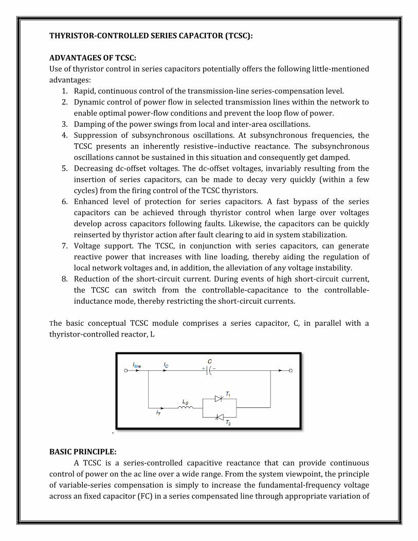
THYRISTOR-CONTROLLED SERIES CAPACITOR (TCSC):
ADVANTAGES OF TCSC:
Use of thyristor control in series capacitors potentially offers the following little-mentioned
advantages:
1. Rapid, continuous control of the transmission-line series-compensation level.
2. Dynamic control of power flow in selected transmission lines within the network to
enable optimal power-flow conditions and prevent the loop flow of power.
3. Damping of the power swings from local and inter-area oscillations.
4. Suppression of subsynchronous oscillations. At subsynchronous frequencies, the
TCSC presents an inherently resistive–inductive reactance. The subsynchronous
oscillations cannot be sustained in this situation and consequently get damped.
5. Decreasing dc-offset voltages. The dc-offset voltages, invariably resulting from the
insertion of series capacitors, can be made to decay very quickly (within a few
cycles) from the firing control of the TCSC thyristors.
6. Enhanced level of protection for series capacitors. A fast bypass of the series
capacitors can be achieved through thyristor control when large over voltages
develop across capacitors following faults. Likewise, the capacitors can be quickly
reinserted by thyristor action after fault clearing to aid in system stabilization.
7. Voltage support. The TCSC, in conjunction with series capacitors, can generate
reactive power that increases with line loading, thereby aiding the regulation of
local network voltages and, in addition, the alleviation of any voltage instability.
8. Reduction of the short-circuit current. During events of high short-circuit current,
the TCSC can switch from the controllable-capacitance to the controllable-
inductance mode, thereby restricting the short-circuit currents.
The basic conceptual TCSC module comprises a series capacitor, C, in parallel with a
thyristor-controlled reactor, L
,
BASIC PRINCIPLE:
A TCSC is a series-controlled capacitive reactance that can provide continuous
control of power on the ac line over a wide range. From the system viewpoint, the principle
of variable-series compensation is simply to increase the fundamental-frequency voltage
across an fixed capacitor (FC) in a series compensated line through appropriate variation of

the firing angle, α. This enhanced voltage changes the effective value of the series-
capacitive reactance.
The impedance of the LC network is given by
𝑍𝑒𝑞 = 𝑋𝐶 𝑋𝐿
𝑋𝐶 + 𝑋𝐿
If ωL > 1/ωC, the the reactance of the FC is less than that of the parallel-connected
variable reactor and that this combination provides a variable-capacitive reactance are
both implied. Moreover, this inductor increases the equivalent-capacitive reactance of the
LC combination above that of the FC.
If ωC - 1/ωL = 0 a resonance develops that results in an infinite-capacitive
impedance an obviously unacceptable condition.
If, however, ωL < 1/ωC, the LC combination provides inductance above the value of
the fixed inductor. This situation corresponds to the inductive-vernier mode of the TCSC
operation.
In the variable-capacitance mode of the TCSC, as the inductive reactance of the
variable inductor is increased, the equivalent-capacitive reactance is gradually decreased.
The minimum equivalent-capacitive reactance is obtained for extremely large inductive
reactance or when the variable inductor is open-circuited, in which the value is equal to the
reactance of the FC itself. The behavior of the TCSC is similar to that of the parallel LC
combination.
The difference is that the LC-combination analysis is based on the presence of pure
sinusoidal voltage and current in the circuit, whereas in the TCSC, because of the voltage
and current in the FC and thyristor-controlled reactor (TCR) are not sinusoidal because of
thyristor switchings.
MODES OF TCSC OPERATION:
BYPASSED-THYRISTOR MODE
BLOCKED-THYRISTOR MODE
PARTIALLY CONDUCTING THYRISTOR, OR VERNIER, MODE

BYPASSED-THYRISTOR MODE:
In this bypassed mode, the thyristors are made to fully conduct with a conduction
angle of 1800. Gate pulses are applied as soon as the voltage across the thyristors reaches
zero and becomes positive, resulting in a continuous sinusoidal of flow current through the
thyristor valves.
The TCSC module behaves like a parallel capacitor–inductor combination. However,
the net current through the module is inductive, for the susceptance of the reactor is
chosen to be greater than that of the capacitor. Also known as the thyristor-switched-
reactor (TSR) mode, the bypassed thyristor mode is distinct from the bypassed-breaker
mode, in which the circuit breaker provided across the series capacitor is closed to remove
the capacitor or the TCSC module in the event of TCSC faults or transient over voltages
across the TCSC.
This mode is employed for control purposes and also for initiating certain protective
functions. Whenever a TCSC module is bypassed from the violation of the current limit, a
finite-time delay, TDelay , must elapse before the module can be reinserted after the line
current falls below the specified limit.
BLOCKED-THYRISTOR MODE:
In this mode, also known as the waiting mode, the firing pulses to the thyristor
valves are blocked. If the thyristors are conducting and a blocking command is given, the
thyristors turn off as soon as the current through them reaches a zero crossing.
The TCSC module is thus reduced to a fixed-series capacitor, and the net TCSC
reactance is capacitive. In this mode, the dc-offset voltages of the capacitors are monitored
and quickly discharged using a dc-offset control without causing any harm to the
transmission-system transformers.

PARTIALLY CONDUCTING THYRISTOR, OR VERNIER, MODE:
This mode allows the TCSC to behave either as a continuously controllable
capacitive reactance or as a continuously controllable inductive reactance. It is achieved by
varying the thyristor-pair firing angle in an appropriate range.
However, a smooth transition from the capacitive to inductive mode is not
permitted because of the resonant region between the two modes.
A variant of this mode is the capacitive-vernier-control mode, in which the
thyristors are fired when the capacitor voltage and capacitor current have opposite
polarity
This condition causes a TCR current that has a direction opposite that of the
capacitor current, thereby resulting in a loop-current flow in the TCSC controller. The loop
current increases the voltage across the FC, effectively enhancing the equivalent-capacitive
reactance and the series-compensation level for the same value of line current.
To preclude resonance, the firing angle α of the forward-facing thyristor, as
measured from the positive reaching a zero crossing of the capacitor voltage, is constrained
in the range of αmin ≤ α ≤ αmax . This constraint provides a continuous vernier control of the
TCSC module reactance. The loop current increases as α is decreased from 1800 to αmin. .
The maximum TCSC reactance permissible with α = αmin. is typically two-and-a-half to
three times the capacitor reactance at fundamental frequency.
Another variant is the inductive-vernier mode, in which the TCSC can be operated
by having a high level of thyristor conduction. In this mode, the direction of the circulating
current is reversed and the controller presents a net inductive impedance
Based on the three modes of thyristor-valve operation, two variants of the TCSC emerge:
Thyristor-switched series capacitor (TSSC), which permits a discrete control of the
capacitive reactance.
Thyristor-controlled series capacitor (TCSC), which offers a continuous control of
capacitive or inductive reactance. (The TSSC, however, is more commonly
employed.)

ANALYSIS OF THE TCSC:
The analysis of TCSC operation in the vernier-control mode is performed based on
the simplified TCSC circuit. Transmission-line current is assumed to be the independent-
input variable and is modeled as an external current source, iS(t). It is further assumed that
the line current is sinusoidal, as derived from actual measurements demonstrating that
very few harmonics exist in the line current. However, the analysis presented in the
following text may be erroneous to the extent that the line current deviates from a purely
sinusoidal nature.
The current through the fixed-series capacitor, C, is expressed as
CdVC
dt= iS(t) − iT(t). u
The switching variable u = 1 when the thyristor valves are conducting, that is, when
the switch S is closed. On the other hand, u = 0 when the thyristors are blocked, that is,
when switch S is open.
The thyristor-valve current, iT(t) , is then described by
LdiT
dt= VC. u
Let the line current, iS(t), be represented by
iS(t) = Im cos ωt
Equations above can be solved with the knowledge of the instants of switching. In
equidistant firing-pulse control, for balanced TCSC operation, the thyristors are switched
on twice in each cycle of line current at instants t1 and t3, given by
t1 = −β
ω and t3 =
(π − β)
ω
where β is the angle of advance (before the forward voltage becomes zero). Or
β = π – α 0 ≤ β ≤ βmax
The firing angle α is generated using a reference signal that can be in phase with the
capacitor voltage. The thyristor switch S turns off at the instants t2 and t4 , defined as
t2 = t1 +σ
ω and t4 = t3 +
σ
ω
where σ is the conduction angle, which is assumed to be the same in both the positive and
the negative cycle of conduction. Also,
σ = 2β Solving TCSC equations results in steady state thyristor currents
iT(t) = k2
k2 − 2 {cos ωt −
cos β
cos k βcos ωr t}
Where
ωr = 1
√LC
k = ωr
ω= √
1
ωL
1
ωC= √
XC
XL
and XC is the nominal reactance of the FC only.
The steady-state capacitor voltage at the instant ωt = -β
VC1 = Im XC
k2 − 1 (sin β − k cosβ tankβ )
At ωt = β, iT = 0 , and the capacitor voltage is given by
vc (ωt = β) = vc2 = −vc1
The capacitor voltage is finally obtained as
VC(t) = Im XC
k2 − 1 (– sin ωt + k
cosβ
cos kβ sin ωr t)
VC(t) = VC2 + Im XC ( sinωt − sin β)
Because the non sinusoidal capacitor voltage, vc , has odd symmetry about the axis ωt = 0,
the fundamental component, VCF is obtained as
𝑉𝐶𝐹 = 4
𝜋 ∫ 𝑉𝐶(𝑡) sin 𝜔𝑡 𝑑(𝜔𝑡)
𝜋/2
0
𝑋𝑇𝐶𝑆𝐶 = 𝑉𝐶𝐹
𝐼𝑚
𝑋𝑇𝐶𝑆𝐶 = 𝑉𝐶𝐹
𝐼𝑚= 𝑋𝐶 −
𝑋𝐶2
(𝑋𝐶 − 𝑋𝐿 ) 2𝛽 + 𝑠𝑖𝑛2𝛽
𝜋+
4𝑋𝐶2
(𝑋𝐶 − 𝑋𝐿 )
𝑐𝑜𝑠2𝛽
𝑘2 − 1 𝑘 tan 𝑘𝛽 − tan 𝛽
𝜋

CAPACITIVE MODE FOR α = 1500

INDUCTIVE MODE FOR α = 1300

BASIC OPERATING CONTROL SCHEMES FOR GCSC, TSSC, AND TCSC:
The function of the operating or "internal" control of the variable impedance type
compensators is to provide appropriate gate drive for the thyristor valve to produce the
compensating voltage or impedance defined by a reference.
The internal control operates the power circuit of the series compensator, enabling
it to function in a self-sufficient manner as a variable reactive impedance. Thus, the power
circuit of the series compensator together with the internal control can be viewed as a
"black box" impedance amplifier, the output of which can be varied from the input with a
low power reference signal.
The reference to the internal control is provided by the "external" or system control,
whose function it is to operate the controllable reactive impedance so as to accomplish
specified compensation objectives of the transmission line. Thus the external control
receives a line impedance, current, power, or angle reference and, within measured system
variables, derives the operating reference for the internal control.
Structurally the internal controls for the three variable impedance type
compensators (GCSC, TCSC, TSSC) could be similar. Succinctly, their function is simply to
define the conduction and/or the blocking intervals of the valve in relation to the
fundamental (power frequency) component of the line current.
This requires the execution of three basic functions:
synchronization to the line current,
turn-on or turn-off delay angle computation, and
gate (firing) signal generation.
These functions obviously can be implemented by different circuit approaches, with
differing advantages and disadvantages. In the following, three possible internal control
schemes are functionally discussed: one for the GCSC, and the other two for the TCSC
power circuit arrangements. Either of the TCSC schemes could be adapted for the TSSC if
subsynchronous resonance would be an application concern.
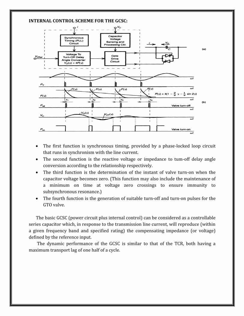
INTERNAL CONTROL SCHEME FOR THE GCSC:
The first function is synchronous timing, provided by a phase-locked loop circuit
that runs in synchronism with the line current.
The second function is the reactive voltage or impedance to tum-off delay angle
conversion according to the relationship respectively.
The third function is the determination of the instant of valve turn-on when the
capacitor voltage becomes zero. (This function may also include the maintenance of
a minimum on time at voltage zero crossings to ensure immunity to
subsynchronous resonance.)
The fourth function is the generation of suitable turn-off and turn-on pulses for the
GTO valve.
The basic GCSC (power circuit plus internal control) can be considered as a controllable
series capacitor which, in response to the transmission line current, will reproduce (within
a given frequency band and specified rating) the compensating impedance (or voltage)
defined by the reference input.
The dynamic performance of the GCSC is similar to that of the TCR, both having a
maximum transport lag of one half of a cycle.

INTERNAL CONTROL SCHEME FOR THE TCSC:
The main consideration for the structure of the internal control operating the power
circuit of the TCSC is to ensure immunity to subsynchronous resonance. Present
approaches follow two basic control philosophies. One is to operate the basic phase locked-
loop (PLL) from the fundamental component of the line current.
In order to achieve this, it is necessary to provide substantial filtering to remove the
super- and, in particular, the subsynchronous components from the line current and, at the
same time, maintain correct phase relationship for proper synchronization. A possible
internal control scheme of this type is shown.
In this arrangement the conventional technique of converting the demanded TCR
current into the corresponding delay angle, which is measured from the peak (or, with a
fixed 90 degree shift, from the zero crossing) of the fundamental line current, is used.
The reference for the demanded TCR current is;, usually provided by a regulation
loop of the external control, which compares the actual capacitive Impedance or
compensating voltage to the reference given for the desired system operation.
The second approach also employs a PLL, synchronized to the line current, for the
generation of the basic timing reference. However, in this method the actual zero crossing
of the capacitor voltage is estimated from the prevailing capacitor voltage and line current
by an angle correction circuit.
The delay angle is then determined from the desired angle and the estimated
correction angle so as to make the TCR conduction symmetrical with respect to the
expected zero crossing.
The desired delay angle in this scheme can be adjusted by a closed-loop controlled
phase shift of the basic time reference provided by the PLL circuit. The delay angle of the
TCR, and thus the compensating capacitive voltage, as in the previous case, is controlled
overall by a regulation loop of the external control in order to meet system operating

requirements. This regulation loop is relatively slow, with a bandwidth just sufficient to
meet compensation requirements (power flow adjustment, power oscillation damping,
etc.). Thus, from the stand point of the angle correction circuit, which by comparison is very
fast (correction takes place in each half cycle), the output of the phase shifter is almost a
steady state reference.
Although control circuit performances are usually heavily dependent on the actual
implementation, the second approach is theoretically more likely to provide faster
response for those applications requiring such response.