Embed Size (px)
Citation preview

1998 Mixed-Signal Products
User’s Guide
SLVU009
IMPORTANT NOTICE
Texas Instruments and its subsidiaries (TI) reserve the right to make changes to their products or to discontinueany product or service without notice, and advise customers to obtain the latest version of relevant informationto verify, before placing orders, that information being relied on is current and complete. All products are soldsubject to the terms and conditions of sale supplied at the time of order acknowledgement, including thosepertaining to warranty, patent infringement, and limitation of liability.
TI warrants performance of its semiconductor products to the specifications applicable at the time of sale inaccordance with TI’s standard warranty. Testing and other quality control techniques are utilized to the extentTI deems necessary to support this warranty. Specific testing of all parameters of each device is not necessarilyperformed, except those mandated by government requirements.
CERTAIN APPLICATIONS USING SEMICONDUCTOR PRODUCTS MAY INVOLVE POTENTIAL RISKS OFDEATH, PERSONAL INJURY, OR SEVERE PROPERTY OR ENVIRONMENTAL DAMAGE (“CRITICALAPPLICATIONS”). TI SEMICONDUCTOR PRODUCTS ARE NOT DESIGNED, AUTHORIZED, ORWARRANTED TO BE SUITABLE FOR USE IN LIFE-SUPPORT DEVICES OR SYSTEMS OR OTHERCRITICAL APPLICATIONS. INCLUSION OF TI PRODUCTS IN SUCH APPLICATIONS IS UNDERSTOOD TOBE FULLY AT THE CUSTOMER’S RISK.
In order to minimize risks associated with the customer’s applications, adequate design and operatingsafeguards must be provided by the customer to minimize inherent or procedural hazards.
TI assumes no liability for applications assistance or customer product design. TI does not warrant or representthat any license, either express or implied, is granted under any patent right, copyright, mask work right, or otherintellectual property right of TI covering or relating to any combination, machine, or process in which suchsemiconductor products or services might be or are used. TI’s publication of information regarding any thirdparty’s products or services does not constitute TI’s approval, warranty or endorsement thereof.
Copyright 1998, Texas Instruments Incorporated

How to Use This Manual
iii Read This First
Preface
Read This First
About This Manual
This User’s Guide describes the universal operational amplifier (op amp) eval-uation module (EVM) with shutdown that can be used to construct many opamp evaluation circuits. Schematics of the EVM and several example circuitsare included.
How to Use This Manual
This document contains the following chapters:
Chapter 1 Introduction
Chapter 2 Schematics
Chapter 3 Board Layout
Chapter 4 Example Circuits
FCC Warning
This equipment is intended for use in a laboratory test environment only. It gen-erates, uses, and can radiate radio frequency energy and has not been testedfor compliance with the limits of computing devices pursuant to subpart J ofpart 15 of FCC rules, which are designed to provide reasonable protectionagainst radio frequency interference. Operation of this equipment in other en-vironments may cause interference with radio communications, in which casethe user at his own expense will be required to take whatever measures maybe required to correct this interference.
Trademarks
TI is a trademark of Texas Instruments Incorporated.

iv
Running Title—Attribute Reference
v Chapter Title—Attribute Reference
Contents
1 Introduction 1-1. . . . . . . . . . . . . . . . . . . . . . . . . . . . . . . . . . . . . . . . . . . . . . . . . . . . . . . . . . . . . . . . . . . . . 1.1 Design Features 1-2. . . . . . . . . . . . . . . . . . . . . . . . . . . . . . . . . . . . . . . . . . . . . . . . . . . . . . . . . . . . 1.2 Power Requirements 1-2. . . . . . . . . . . . . . . . . . . . . . . . . . . . . . . . . . . . . . . . . . . . . . . . . . . . . . . .
2 Schematics 2-1. . . . . . . . . . . . . . . . . . . . . . . . . . . . . . . . . . . . . . . . . . . . . . . . . . . . . . . . . . . . . . . . . . . . . 2.1 Area Schematics 2-2. . . . . . . . . . . . . . . . . . . . . . . . . . . . . . . . . . . . . . . . . . . . . . . . . . . . . . . . . . .
3 Board Layout 3-1. . . . . . . . . . . . . . . . . . . . . . . . . . . . . . . . . . . . . . . . . . . . . . . . . . . . . . . . . . . . . . . . . . . 3.1 Physical Considerations 3-2. . . . . . . . . . . . . . . . . . . . . . . . . . . . . . . . . . . . . . . . . . . . . . . . . . . . .
3.1.1 Area 100 – SOIC 3-2. . . . . . . . . . . . . . . . . . . . . . . . . . . . . . . . . . . . . . . . . . . . . . . . . . . . 3.1.2 Area 200 – MSOP 3-2. . . . . . . . . . . . . . . . . . . . . . . . . . . . . . . . . . . . . . . . . . . . . . . . . . . 3.1.3 Area 300 – SOIC 3-2. . . . . . . . . . . . . . . . . . . . . . . . . . . . . . . . . . . . . . . . . . . . . . . . . . . . 3.1.4 Area 400 – SOT23-6 3-2. . . . . . . . . . . . . . . . . . . . . . . . . . . . . . . . . . . . . . . . . . . . . . . . .
3.2 Component Placement 3-3. . . . . . . . . . . . . . . . . . . . . . . . . . . . . . . . . . . . . . . . . . . . . . . . . . . . . . 3.3 Board Layout 3-4. . . . . . . . . . . . . . . . . . . . . . . . . . . . . . . . . . . . . . . . . . . . . . . . . . . . . . . . . . . . . .
4 Example Circuits 4-1. . . . . . . . . . . . . . . . . . . . . . . . . . . . . . . . . . . . . . . . . . . . . . . . . . . . . . . . . . . . . . . . 4.1 Schematic Conventions 4-2. . . . . . . . . . . . . . . . . . . . . . . . . . . . . . . . . . . . . . . . . . . . . . . . . . . . . 4.2 Sallen-Key Low-Pass Filter 4-3. . . . . . . . . . . . . . . . . . . . . . . . . . . . . . . . . . . . . . . . . . . . . . . . . . 4.3 Sallen-Key High-Pass Filter 4-4. . . . . . . . . . . . . . . . . . . . . . . . . . . . . . . . . . . . . . . . . . . . . . . . . . 4.4 Inverting Amplifier 4-6. . . . . . . . . . . . . . . . . . . . . . . . . . . . . . . . . . . . . . . . . . . . . . . . . . . . . . . . . . 4.5 Noninverting Amplifier 4-7. . . . . . . . . . . . . . . . . . . . . . . . . . . . . . . . . . . . . . . . . . . . . . . . . . . . . . . 4.6 Two Operational Amplifier Instrumentation Amplifier 4-8. . . . . . . . . . . . . . . . . . . . . . . . . . . . . 4.7 Differential Amplifier 4-10. . . . . . . . . . . . . . . . . . . . . . . . . . . . . . . . . . . . . . . . . . . . . . . . . . . . . . . .

Running Title—Attribute Reference
vi
Figures
2–1 Area 100 Schematic – SOIC (14 pin) 2-2. . . . . . . . . . . . . . . . . . . . . . . . . . . . . . . . . . . . . . . . . . . . 2–2 Area 200 Schematic – MSOP (10 pin) 2-3. . . . . . . . . . . . . . . . . . . . . . . . . . . . . . . . . . . . . . . . . . . 2–3 Area 300 Schematic – SOIC (8 pin) 2-4. . . . . . . . . . . . . . . . . . . . . . . . . . . . . . . . . . . . . . . . . . . . . 2–4 Area 400 Schematic – SOT23-6 (6 pin) 2-4. . . . . . . . . . . . . . . . . . . . . . . . . . . . . . . . . . . . . . . . . . 3–1 Component Placement 3-3. . . . . . . . . . . . . . . . . . . . . . . . . . . . . . . . . . . . . . . . . . . . . . . . . . . . . . . . 3–2 Board Layout Top 3-4. . . . . . . . . . . . . . . . . . . . . . . . . . . . . . . . . . . . . . . . . . . . . . . . . . . . . . . . . . . . . 3–3 Board Layout Bottom 3-5. . . . . . . . . . . . . . . . . . . . . . . . . . . . . . . . . . . . . . . . . . . . . . . . . . . . . . . . . . 4–1 Sallen-Key Low-Pass Filter with Dual Supply Using Area 100 4-3. . . . . . . . . . . . . . . . . . . . . . . 4–2 Sallen-Key High-Pass Filter with Single Supply Using Area 200 4-5. . . . . . . . . . . . . . . . . . . . . 4–3 Inverting Amplifier with Dual Supply Using Area 300 4-6. . . . . . . . . . . . . . . . . . . . . . . . . . . . . . . 4–4 Noninverting Amplifier with Single Supply Using Area 400 4-7. . . . . . . . . . . . . . . . . . . . . . . . . . 4–5 Two Operational Amplifier Instrumentation Amplifier with Single Supply
Using Area 200 4-9. . . . . . . . . . . . . . . . . . . . . . . . . . . . . . . . . . . . . . . . . . . . . . . . . . . . . . . . . . . . . . . 4–6 Single Operational Amplifier Differential Amplifier with Single Supply
Using Area 300 4-10. . . . . . . . . . . . . . . . . . . . . . . . . . . . . . . . . . . . . . . . . . . . . . . . . . . . . . . . . . . . . .

1-1Introduction
Introduction
This User’s Guide describes a universal operational amplifier (op amp)evaluation module (EVM) with shutdown (#SLOP224). The EVM simplifiesevaluation of Texas Instruments surface-mount op amps with the shutdownfeature.
Topic Page
1.1 Design Features 1–2. . . . . . . . . . . . . . . . . . . . . . . . . . . . . . . . . . . . . . . . . . . . . .
1.2 Power Requirements 1–2. . . . . . . . . . . . . . . . . . . . . . . . . . . . . . . . . . . . . . . . . .
Chapter 1
Design Features
1-2 Introduction
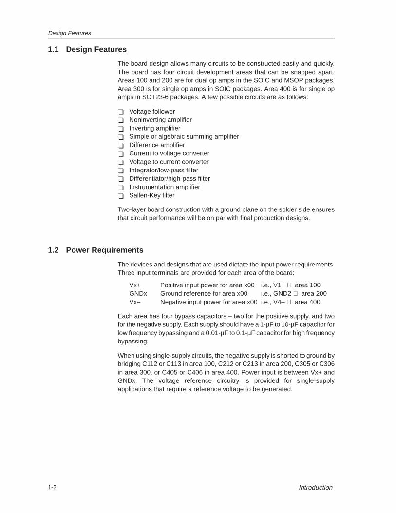
1.1 Design Features
The board design allows many circuits to be constructed easily and quickly.The board has four circuit development areas that can be snapped apart.Areas 100 and 200 are for dual op amps in the SOIC and MSOP packages.Area 300 is for single op amps in SOIC packages. Area 400 is for single opamps in SOT23-6 packages. A few possible circuits are as follows:
Voltage follower Noninverting amplifier Inverting amplifier Simple or algebraic summing amplifier Difference amplifier Current to voltage converter Voltage to current converter Integrator/low-pass filter Differentiator/high-pass filter Instrumentation amplifier Sallen-Key filter
Two-layer board construction with a ground plane on the solder side ensuresthat circuit performance will be on par with final production designs.
1.2 Power Requirements
The devices and designs that are used dictate the input power requirements.Three input terminals are provided for each area of the board:
Vx+ Positive input power for area x00 i.e., V1+ ⇒ area 100GNDx Ground reference for area x00 i.e., GND2 ⇒ area 200Vx– Negative input power for area x00 i.e., V4– ⇒ area 400
Each area has four bypass capacitors – two for the positive supply, and twofor the negative supply. Each supply should have a 1-µF to 10-µF capacitor forlow frequency bypassing and a 0.01-µF to 0.1-µF capacitor for high frequencybypassing.
When using single-supply circuits, the negative supply is shorted to ground bybridging C112 or C113 in area 100, C212 or C213 in area 200, C305 or C306in area 300, or C405 or C406 in area 400. Power input is between Vx+ andGNDx. The voltage reference circuitry is provided for single-supplyapplications that require a reference voltage to be generated.
2-1Schematics
Schematics
This chapter contains schematics and pin-outs for each of the four areas.
Topic Page
2.1 Area Schematics 2–1. . . . . . . . . . . . . . . . . . . . . . . . . . . . . . . . . . . . . . . . . . . . . .
Chapter 2
Area Schematics
2-2 Schematics
2.1 Area Schematics
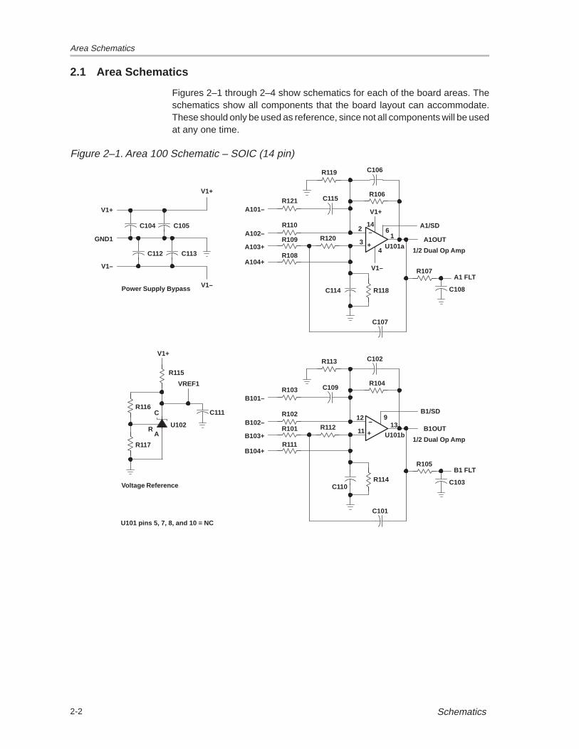
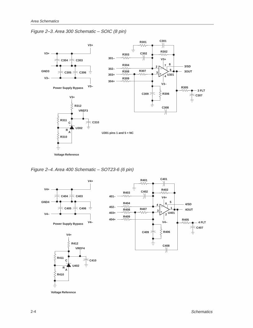
Figures 2–1 through 2–4 show schematics for each of the board areas. Theschematics show all components that the board layout can accommodate.These should only be used as reference, since not all components will be usedat any one time.
Figure 2–1. Area 100 Schematic – SOIC (14 pin)
C104 C105
C112 C113
V1+
V1–
V1+
GND1
V1–
Power Supply Bypass
+
–14
1
43
2
V1+
V1–
R106C115
R119 C106
R121
R110
R120R109
R108
R118C114
C107
A1OUT
1/2 Dual Op Amp
A101–
A102–
A103+
A104+
+
– 1311
12
R104C109
R113 C102
R103
R102
R112R101
R111
R114C110
C101
B1OUT
1/2 Dual Op Amp
B101–
B102–
B103+
B104+
R116C
RA
U102
R117
Voltage Reference
V1+
VREF1
U101a
U101b
R115
A1/SD
C108
R107A1 FLT
B1/SD9
C103
R105B1 FLT
C111
U101 pins 5, 7, 8, and 10 = NC
6

Area Schematics
2-3Schematics
Figure 2–2. Area 200 Schematic – MSOP (10 pin)
B2/SD
C204 C205
C212 C213
V2+
V2–
V2+
GND2
V1–
Power Supply Bypass
+
–10
1
43
2
V2+
V2–
R206C215
R219 C206
R221
R210
R220R209
R208
R218C214
C207
A2OUT
1/2 Dual Op Amp
A201–
A202–
A203+
A204+
+
–
R204C209
R213 C202
R203
R202
R212R201
R211
R214C210
C201
B2OUT
1/2 Dual Op Amp
B201–
B202–
B203+
B204+
R216C
RA
U202
R217
Voltage Reference
U201a
U201b
V2+
VREF2
R215
97
8
C208
R207A2 FLT
C203
R205B2 FLT
A2/SD5
C2116
Area Schematics
2-4 Schematics
Figure 2–3. Area 300 Schematic – SOIC (8 pin)
C304 C303
C305 C306
V3+
V3–
V3+
GND3
V3–
Power Supply Bypass
+
–7
6
43
2
V3+
V3–
R302C302
R301 C301
R303
R304
R307R308
R309
R306C309
C308
3OUT
301–
302–
303+
304+
R311C
RA
U302
R310
Voltage Reference
U301
V3+
VREF3
R312
C307
R3053 FLT
3/SD8
C310
U301 pins 1 and 5 = NC
Figure 2–4. Area 400 Schematic – SOT23-6 (6 pin)
C404 C403
C405 C406
V4+
V4–
V4+
GND4
V4–
Power Supply Bypass
+
–6
1
23
4
V4+
V4–
R402C402
R401 C401
R403
R404
R407R408
R409
R406C409
C408
4OUT
401–
402–
403+
404+
R411C
RA
U402
R410
Voltage Reference
U401
V4+
VREF4
R412
C407
R4054 FLT
4/SD5
C410
3-1Board Layout
Board Layout
This chapter shows the universal op amp EVM with shutdown board layout,and describes the relationships between the four areas.
Topic Page
3.1 Physical Consideration 3–2. . . . . . . . . . . . . . . . . . . . . . . . . . . . . . . . . . . . . . . .
3.2 Component Placement 3–3. . . . . . . . . . . . . . . . . . . . . . . . . . . . . . . . . . . . . . . .
3.3 Board Layout 3–4. . . . . . . . . . . . . . . . . . . . . . . . . . . . . . . . . . . . . . . . . . . . . . . . .
Chapter 3

Physical Considerations
3-2 Board Layout
3.1 Physical Considerations
The EVM board has four circuit development areas. Each area can beseparated from the others by breaking along the score lines. The circuit layoutin each area supports an op amp package, voltage reference, and ancillarydevices. The op amp package is unique to each area as described in thefollowing paragraphs. The voltage reference and supporting devices are thesame for all areas. Surface-mount or through-hole components can be usedfor all capacitors and resistors on the board.
The voltage reference can be either surface-mount or through-hole. If surfacemount is desired, the TLV431ACDBV5 or TLV431AIDBV5 adjustable shuntregulators can be used. If through hole is desired, the TLV431ACLP,TLV431AILP, TL431CLP, TL431ACLP, TL431ILP or TL431AILP adjustableshunt regulators can be used. Refer to Texas Instruments’ Power SupplyCircuits Data Book (literature number SLVD002) for details on usage of theseshunt regulators.
Each passive component (resistor or capacitor) has a surface mount 1206footprint with through holes at 0.2″ spacing on the outside of the 1206 pads.Therefore, either surface-mount or through-hole parts can be used.
3.1.1 Area 100 – SOIC
Area 100 uses 1xx reference designators, and is compatible with dual op ampswith shutdown packaged as a 14-pin SOIC. This surface-mount package isdesignated by a D suffix in TI part numbers, as in TLV2463CD, TLV2363ID,TLV2263AID, etc. Refer to Figure 2–1 for a schematic.
3.1.2 Area 200 – MSOP
Area 200 uses 2xx reference designators, and is compatible with dual op ampswith shutdown packaged as a 10-pin MSOP. The MSOP package isdesignated by a DGS suffix in TI part numbers, as in TLV2463CDGS. Referto Figure 2–2 for a schematic.
3.1.3 Area 300 – SOIC
Area 300 uses 3xx reference designators, and is compatible with single opamps with shutdown packaged in the 8-pin SOIC package. This surface-mount package is designated by a D suffix in TI part numbers, as inTLV2461CD. Refer to Figure 2–3 for a schematic.
3.1.4 Area 400 – SOT23-6
Area 400 uses 4xx reference designators, and is compatible with single opamps with shutdown packaged in the 6-pin SOT-23 package. Thissurface-mount package is designated by a DBV suffix in TI part numbers, asin TLV2460CDBV. Refer to Figure 2–4 for a schematic.
Component Placement
3-3Board Layout
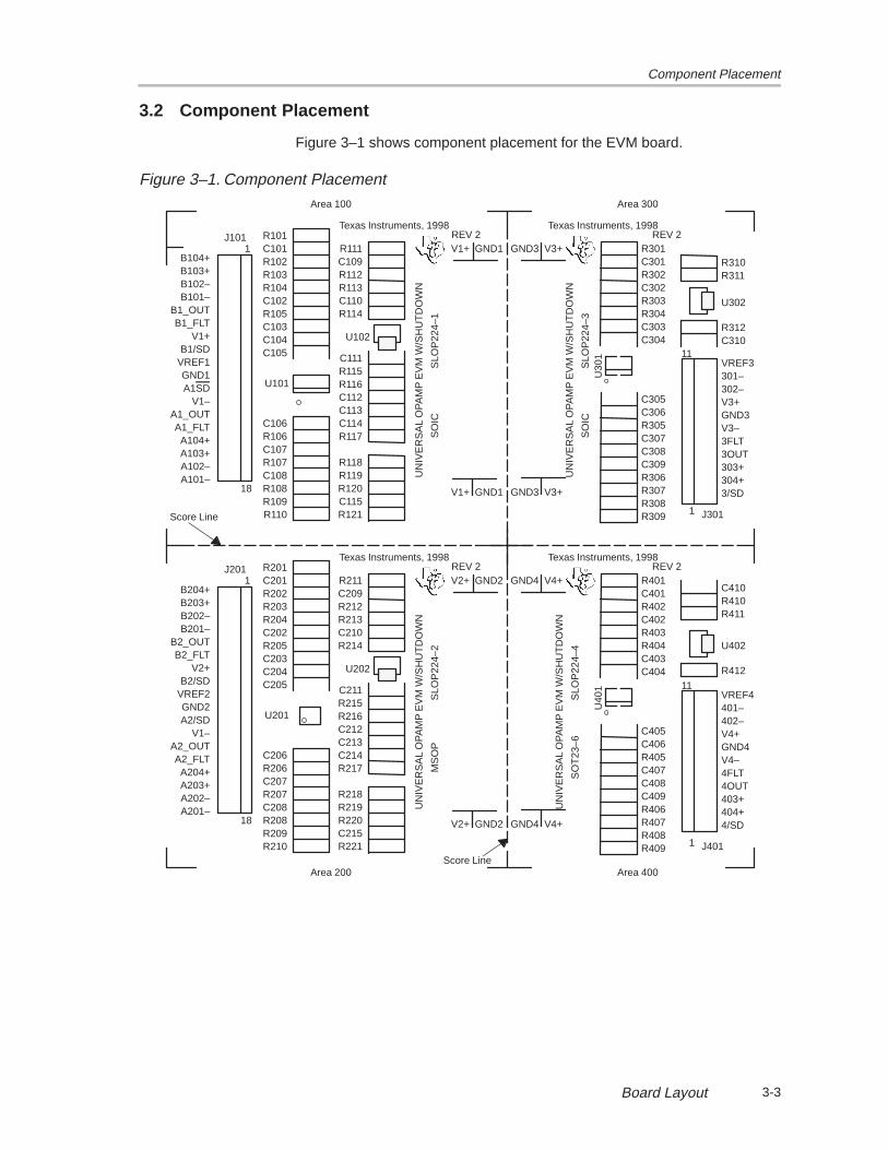
3.2 Component Placement
Figure 3–1 shows component placement for the EVM board.
Figure 3–1. Component Placement
V2+ GND2
Area 100
B104+B103+B102–B101–
B1_OUTB1_FLT
V1+B1/SD
VREF1GND1A1SD
V1–A1_OUTA1_FLT
A104+A103+A102–A101–
1
18
J101 R101C101R102R103R104C102R105C103C104C105
U101
C106R106C107R107C108R108R109R110
R111C109R112R113C110R114
C111R115R116C112C113C114R117
R118R119R120C115R121
Texas Instruments, 1998
UN
IVE
RS
AL
OP
AM
P E
VM
W/S
HU
TD
OW
N
SO
ICS
LOP
224–
1
V1+ GND1
REV 2
U102
B204+B203+B202–B201–
B2_OUTB2_FLT
V2+B2/SD
VREF2GND2A2/SD
V1–A2_OUTA2_FLT
A204+A203+A202–A201–
1
18
J201 R201C201R202R203R204C202R205C203C204C205
U201
C206R206C207R207C208R208R209R210
R211C209R212R213C210R214
C211R215R216C212C213C214R217
R218R219R220C215R221
Texas Instruments, 1998
UN
IVE
RS
AL
OP
AM
P E
VM
W/S
HU
TD
OW
N
MS
OP
SLO
P22
4–2
V2+ GND2
REV 2
U202
V1+ GND1
Texas Instruments, 1998
UN
IVE
RS
AL
OP
AM
P E
VM
W/S
HU
TD
OW
N
SO
ICS
LOP
224–
3
REV 2GND3 V3+ R301
C301R302C302R303R304C303C304
R310R311
U302
R312C310
U30
1
C305C306R305C307C308C309R306R307R308R309
VREF3301–302–V3+GND3V3–3FLT3OUT303+304+3/SD
11
1
GND3 V3+
Texas Instruments, 1998REV 2
GND4 V4+ R401C401R402C402R403R404C403C404
C410R410R411
U402
R412
U40
1
C405C406R405C407C408C409R406R407R408R409
VREF4401–402–V4+GND4V4–4FLT4OUT403+404+4/SD
11
1
GND4 V4+
UN
IVE
RS
AL
OP
AM
P E
VM
W/S
HU
TD
OW
N
SO
T23
–6S
LOP
224–
4
J301
J401Score Line
Area 300
Area 200 Area 400
Score Line
Board Layout
3-4 Board Layout
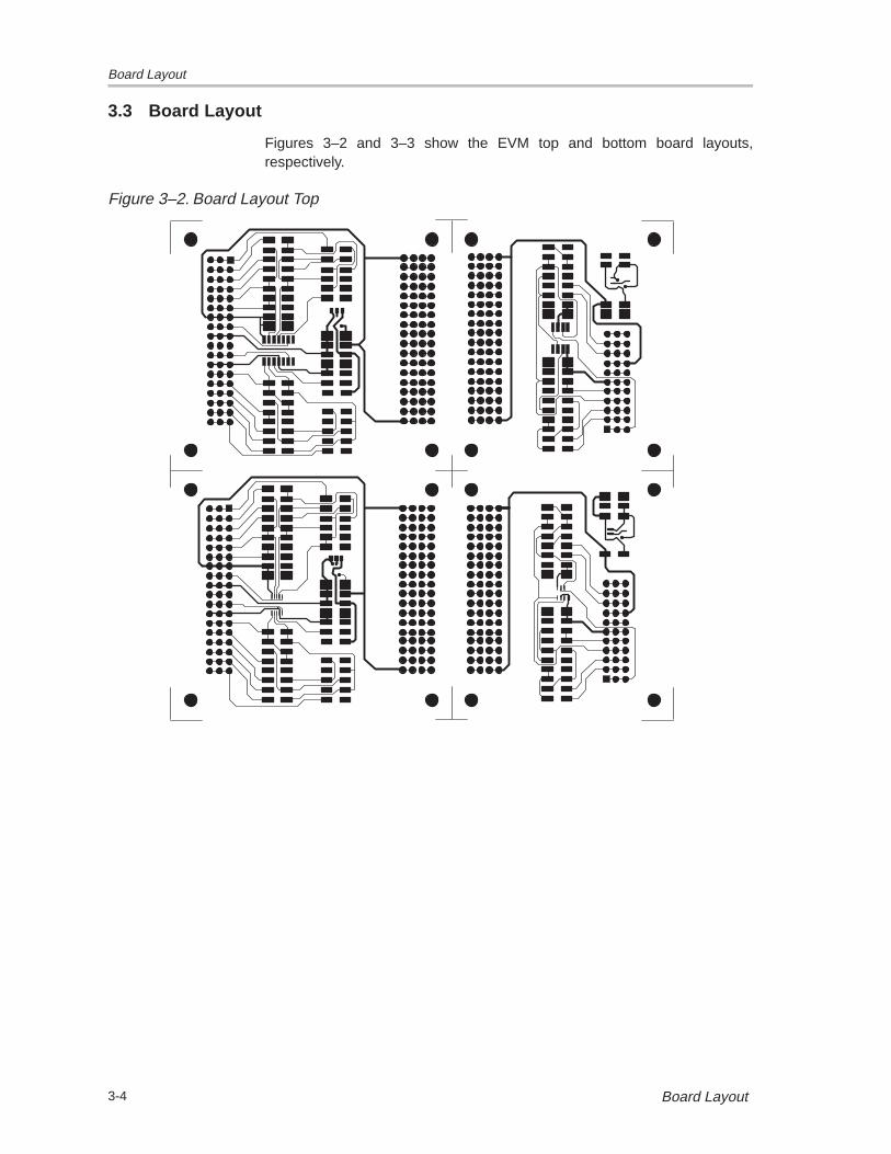
3.3 Board Layout
Figures 3–2 and 3–3 show the EVM top and bottom board layouts,respectively.
Figure 3–2. Board Layout Top

Board Layout
3-5Board Layout
Figure 3–3. Board Layout Bottom

3-6 Board Layout

4-1Example Circuits
Example Circuits
This chapter shows and discusses several example circuits that can beconstructed using the universal operational amplifier EVM. The circuits are allclassic designs that can be found in most operational amplifier design books.
Topic Page
4.1 Schematic Conventions 4–2. . . . . . . . . . . . . . . . . . . . . . . . . . . . . . . . . . . . . . .
4.2 Sallen-Key Low-Pass Filter 4–3. . . . . . . . . . . . . . . . . . . . . . . . . . . . . . . . . . . .
4.3 Sallen-Key High-Pass Filter 4–5. . . . . . . . . . . . . . . . . . . . . . . . . . . . . . . . . . . .
4.4 Inverting Amplifier 4–7. . . . . . . . . . . . . . . . . . . . . . . . . . . . . . . . . . . . . . . . . . . .
4.5 Noninverting Amplifier 4–8. . . . . . . . . . . . . . . . . . . . . . . . . . . . . . . . . . . . . . . .
4.6 Two Operational Amplifier Instrumentation Amplifiers 4–9. . . . . . . . . . .
4.7 Differential AMplifier 4–11. . . . . . . . . . . . . . . . . . . . . . . . . . . . . . . . . . . . . . . . .
Chapter 4

Schematic Conventions
4-2 Example Circuits
4.1 Schematic Conventions
Figures 4–1 through 4–6 show schematic examples of circuits that can beconstructed using the universal operational amplifier EVM with shutdown. Thecomponents that are placed on the board are shown in bold. Unusedcomponents are blanked out. Jumpers and other changes are noted. Theseexamples are only a few of the many circuits that can be built.
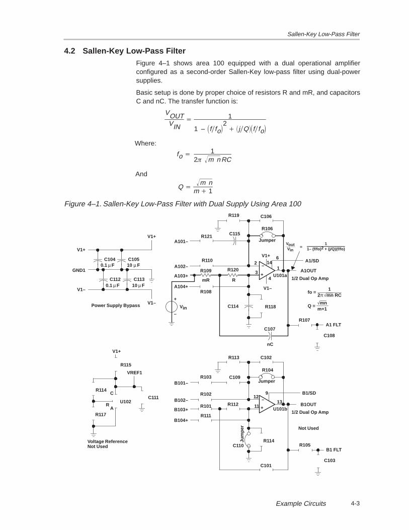
Sallen-Key Low-Pass Filter
4-3Example Circuits
4.2 Sallen-Key Low-Pass FilterFigure 4–1 shows area 100 equipped with a dual operational amplifierconfigured as a second-order Sallen-Key low-pass filter using dual-powersupplies.
Basic setup is done by proper choice of resistors R and mR, and capacitorsC and nC. The transfer function is:
VOUTVIN
1
1 – ffo2 jQffo
Where:
fo 12 m n RC
And
Q m n
m 1
Figure 4–1. Sallen-Key Low-Pass Filter with Dual Supply Using Area 100
C104 C105
C112 C113
V1+
V1–
V1+
GND1
V1–
Power Supply Bypass
+
–14
1
43
2
V1+
V1–
R106C115
R119 C106
R121
R110
R120R109
R108
R118C114
C107
A1OUT
1/2 Dual Op Amp
A101–
A102–
A103+
A104+
+
– 1311
12
R104
C109
R113 C102
R103
R102
R112R101
R111
R114C110
C101
B1OUT
1/2 Dual Op Amp
B101–
B102–
B103+
B104+
R114C
RA
U102
R117
Voltage Reference
V1+
VREF1
U101a
U101b
R115
Jumper
+
–
mR R
nC
Jumper
Jum
per
Not Used
Not Used
VoutVin
Vin
=1
1– (f/fo) 2 + (j/Q)(f/fo)
fo =1
2π √mn RC
Q =√mnm+1
0.1 µ F 10 µ F
0.1 µ F 10 µ F
6A1/SD
R107A1 FLT
C108
9 B1/SD
R105B1 FLT
C103
C111

Sallen-Key High-Pass Filter
4-4 Example Circuits
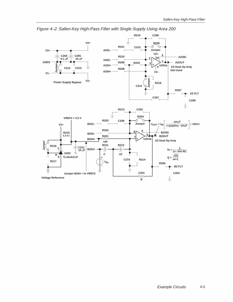
4.3 Sallen-Key High-Pass Filter
Figure 4–2 shows area 200 equipped with a dual operational amplifier config-ured as a second-order Sallen-Key high-pass filter using single-supply powerinput.
Basic setup is done by proper choice of resistors R and mR, and capacitorsC and nC. Note that capacitors should be used for components R211 andR212, and a resistor for C201. The transfer function for the circuit as shownis:
VOUT VIN
– ffo2
1 jQffo– ffo2 VREF2
Where:fo
12 m n RC
And
Q m n
n 1
The TL431 adjustable precision shunt regulator, configured as shown,provides a low impedance reference for the circuit at about 1/2 V2+ in a 5 Vsystem. Another option is to adjust resistors R216 and R217 for the desiredVREF2 voltage. The formula for calculating VREF2 is:
VREF2 2.50 VR216 R217R217
Sallen-Key High-Pass Filter
4-5Example Circuits
Figure 4–2. Sallen-Key High-Pass Filter with Single Supply Using Area 200
C204 C205
C212 C213
V2+
V2–
V2+
GND2
V1–
Power Supply Bypass
+
–10
1
43
2
V2+
V2–
R206
C215
R219 C206
R221
R210
R220R209
R208
R218C214
C207
A2OUT
1/2 Dual Op Amp
A201–
A202–
A203+
A204+
+
–
R204
C209
R213 C202
R203
R202
R201
R211
R214C210
C201
B2OUT
1/2 Dual Op Amp
B201–
B202–
B204+
B203+R216
C
RA
U202
R217
Voltage Reference
U201a
U201b
V2+
VREF2 = 2.5 V
R2159
7
8
+
–
Vin
Jumper
Not Used
Jum
per
Jum
per
R212
C nC
R
Jumper
mR
TL431ACLP
Jum
per
0.1 µF 10 µF
fo =1
2π √mn RC
Q =√mnm+1
VOUT = VIN–(f/fo) 2
1+(j/Q)(f/fo) – (f/fo) 2 + VREF2
Jumper B204 + to VREF2
2.2 kΩ
5A2/SD
A2 FLT
6B2/SD
B2 FLT
C21110 µF
R205
C203
R207
C208
Inverting Amplifier
4-6 Example Circuits
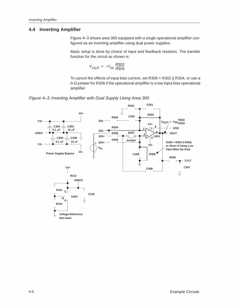
4.4 Inverting Amplifier
Figure 4–3 shows area 300 equipped with a single operational amplifier con-figured as an inverting amplifier using dual power supplies.
Basic setup is done by choice of input and feedback resistors. The transferfunction for the circuit as shown is:
VOUT –VINR302R304
To cancel the effects of input bias current, set R306 = R302 || R304, or use a0-Ω jumper for R306 if the operational amplifier is a low input bias operationalamplifier.
Figure 4–3. Inverting Amplifier with Dual Supply Using Area 300
C304 C303
C305 C306
V3+
V3–
V3+
GND3
V3–
Power Supply Bypass
+
–7
6
43
2
V3+
V3–
R302C302
R301 C301
R303
R304
R307R308
R309
R306C309
C308
3OUT
301–
302–
303+
304+
R311C
RA
U302
R310
Voltage Reference
U301
V3+
VREF3
R312
+
–
Vin
VOUT = –VINR302R304
R306 = R302 II R304,or Short if Using LowInput Bias Op Amp
Not Used
0.1 µF 10 µF
0.1 µF 10 µF
8 3/SD
3 FLTR305
C307
C310
Jumper

Noninverting Amplifier
4-7Example Circuits
4.5 Noninverting Amplifier
Figure 4–4 shows area 400 equipped with a single operational amplifierconfigured as a noninverting amplifier with single-supply power input.
Basic setup is done by choice of input and feedback resistors. The transferfunction for the circuit as shown is:
VOUT VIN 1 R402R404 VREF4
The input signal must be referenced to VREF4.
To cancel the effects of input bias current, set R409 = R402 || R404, or use a0-Ω jumper for R409 if the operational amplifier is a low input bias operationalamplifier.
The TL431 adjustable precision shunt regulator, configured as shown,provides a low impedance reference for the circuit at about 1/2 V4+ in a 3 Vsystem. Another option is to adjust resistors R410 and R411 for the desiredVREF4 voltage. The formula for calculating VREF4 is:
VREF4 1.24 VR411 R410R410
Figure 4–4. Noninverting Amplifier with Single Supply Using Area 400
C404 C403
C405 C406
V4+
V4–
V4+
GND4
V4–
Power Supply Bypass
+
–6
1
23
4
V4+
V4–
R402C402
R401 C401
R403
R404
R407R408
R409
R406C409
C408
4OUT
401–
402–
403+
404+
R411C
RA
U402 = TLV431ACDBV5
R410
Voltage Reference
U401
V4+
VREF4 = 1.24 V
R414
+
–
Vin
Jum
per
0.1 µF 10 µF
Jum
per
Jumper 402 – to VREF4VOUT = VIN
R405R407
R409 = R402 II R404,or Short if Using Low InputBias Op Amp
Input Signal WithReference to VREF4
2.2 kΩ
( )+1 + VREF4
54/SD
4 FLTR405
C407C41010 µF
Two Operational Amplifier Instrumentation Amplifier
4-8 Example Circuits
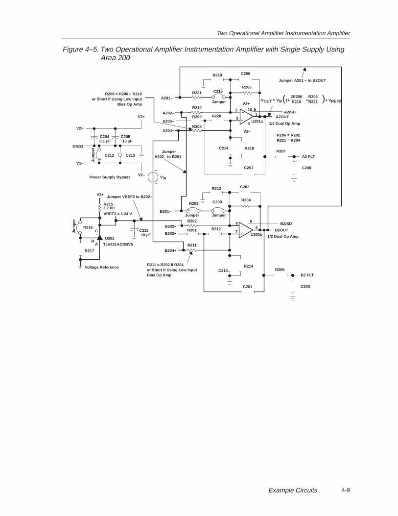
4.6 Two Operational Amplifier Instrumentation Amplifier
Figure 4–5 shows area 200 equipped with a dual operational amplifier config-ured as a two-operational-amplifier instrumentation amplifier using a voltagereference and single power supply.
Basic setup is done by choice of input and feedback resistors. The transferfunction for the circuit as shown is:
VOUT VIN 1 2R206R210
R206R221 VREF2
WhereR206 = R202 and R221 = R204
To cancel the effects of input bias current, set R208 = R206 || R210 and setR211 = R202 ||R204, or use a 0-Ω jumper for R208 and R211 if the operationalamplifier is a low input bias operational amplifier.
The TLV431 adjustable precision shunt regulator, configured as shown,provides a low impedance reference for the circuit at about 1/2 V2+ in a 3 Vsystem. Another option is to adjust resistors R216 and R217 for the desiredVREF2 voltage. The formula for calculating VREF2 is:
VREF2 1.24 VR216 R217R217
Two Operational Amplifier Instrumentation Amplifier
4-9Example Circuits
Figure 4–5. Two Operational Amplifier Instrumentation Amplifier with Single Supply Using Area 200
C204 C205
C212 C213
V2+
V2–
V2+
GND2
V1–
Power Supply Bypass
+
–10
1
43
2
V2+
V2–
R206C215
R219 C206
R221
R210
R220R209
R208
R218C214
C207
A2OUT
1/2 Dual Op Amp
A201–
A202–
A203+
A204+
+
–
R204C209
R213 C202
R203
R202
R201
R211
R214C210
C201
B2OUT
1/2 Dual Op Amp
B201–
B202–
B204+
B203+
R216C
RA
U202
R217
Voltage Reference
U201a
U201b
V2+
VREF2 = 1.24 V
R215
97
8
+
–
Vin
Jumper
Jum
per
R212
TLV431ACDBV5
Jum
per
0.1 µF 10 µF
JumperJumper
VOUT = Vin(1+ + )+ VREF22R206R210
R206R221
Jumper A201 – to B2OUT
R206 = R202R221 = R204
R211 = R202 II R204or Short if Using Low InputBias Op Amp
Jumper VREF2 to B202–
JumperA202– to B201–
R208 = R206 II R210or Short if Using Low Input
Bias Op Amp
2.2 kΩ
6B2/SD
B2 FLTR205
C203
5A2/SD
A2 FLTR207
C208
C21110 µF

Differential Amplifier
4-10 Example Circuits
4.7 Differential Amplifier
Figure 4–6 shows area 300 equipped with a single operational amplifierconfigured as a differential amplifier using a voltage reference and singlepower supply.
Basic setup is done by choice of input and feedback resistors. The transferfunction for the circuit as shown is:
VOUT VIN R302R304 VREF3
WhereR302R304
R309R308
The TLV431 adjustable precision shunt regulator, configured as shown,provides a low impedance reference for the circuit at about 1/2 V3+ in a 3 Vsystem. Another option is to adjust resistors R311 and R310 for the desiredVREF3 voltage. The formula for calculating VREF3 is:
VREF3 1.24 VR311 R310R310
Figure 4–6. Single Operational Amplifier Differential Amplifier with Single Supply UsingArea 300
C304 C303
C306
V3+
V3–
V3+
GND3
V3–
Power Supply Bypass
+
–7
6
43
2
V3+
V3–
R302C302
R301 C301
R303
R304
R319R308
R309
R306C309
C308
3OUT
301–
302–
303+
304+
R311C
RA
U302
R310
Voltage Reference
U301
V3+
VREF3 = 1.24 V
R312
+
–Vin
Vout = VinR302R304
R302R304
Jum
per
Jumper
TLV431ACDBV5
Jumper 304+ to VREF3
= R309R308
( ) + VREF3
0.1 µF 10 µF
2.2 kΩ3 FLT
R305
C307
8 3/SD
C305
C31010 µF