Embed Size (px)
Citation preview
Universal Socket Connectivity
For Embedded Modems SocketModem – MT5600SMI
SocketModem – MT5656SMI
SocketModem – MT5634SMI
SocketModem – MT2456SMI-22
SocketModem IP – MT2456SMI-IP
SocketEthernet IP – MTXCSEM
SocketModem ISDN – MT128SMI
SocketModem GPRS – MTSMC-G
SocketModem CDMA – MTSMC-C
SocketWireless Bluetooth® – MTS2BTSMI
Hardware Guide for Developers
Copyright and Technical Support
Multi-Tech Systems, Inc. Universal Socket Hardware Guide for Developers (S000342C) 2
Universal Socket Connectivity Developer's Guide PN S000342C, Version C Copyright This publication may not be reproduced, in whole or in part, without prior expressed written permission from Multi-Tech Systems, Inc. All rights reserved. Copyright © 2004 by Multi-Tech Systems, Inc. Multi-Tech Systems, Inc. makes no representations or warranties with respect to the contents hereof and specifically disclaim any implied warranties of merchantability or fitness for any particular purpose. Furthermore, Multi-Tech Systems, Inc. reserves the right to revise this publication and to make changes from time to time in the content hereof without obligation of Multi-Tech Systems, Inc. to notify any person or organization of such revisions or changes.
Revisions Revision Level Date Description A 06/17/04 Initial release of Universal Socket Connectivity hardware guide. B 10/01/04 Add SocketWireless with Bluetooth Technology chapter. Changed pinouts:
TXCLK to TCLK and RXCLK to RCLK. Added the schematics for the MT128SMI. Added note to the SocketEthernet IP filtering drawing. C 11/11/04 Revised GSM/GPRS mechanical drawing. More information location information
about AT commands, fax commands, and voice commands. Update Bluetooth chapter.
Trademarks Trademarks of Multi-Tech Systems, Inc. are SocketModem, SocketWireless, and the Multi-Tech logo. Microsoft and Windows are registered trademarks or trademarks of Microsoft Corporation in the United States and/or other countries. Bluetooth is a registered trademark of Bluetooth.
Patents This device covered by one or more of the following patents: 6,031,867; 6,012,113; 6,009,082; 5,905,794; 5,864,560; 5,815,567; 5,815,503; 5,812,534; 5,809,068; 5,790,532; 5,764,628; 5,764,627; 5,754,589; 5,724,356; 5,673,268; 5,673,257; 5,644,594; 5,628,030; 5,619,508; 5,617,423; 5,600,649; 5,592,586; 5,577,041; 5,574,725; 5,559,793; 5,546,448; 5,546,395; 5,535,204; 5,500,859; 5,471,470; 5,463,616; 5,453,986; 5,452,289; 5,450,425; 5,355,365; 5,309,562; 5,301,274. Other Patents Pending. World Headquarters Multi-Tech Systems, Inc. 2205 Woodale Drive Mounds View, Minnesota 55112 Phone: 763-785-3500 or 800-328-9717 Fax: 763-785-9874
Technical Support Country By Email By Phone France: [email protected] (33) 1-64 61 09 81 India: [email protected] 91 (124) 6340778 U.K.: [email protected] (44) 118 959 7774 U.S. and Canada: [email protected] (800) 972-2439 Rest of the World: [email protected] (763) 717-5863 Internet Address: http://www.multitech.com
Table of Contents
Multi-Tech Systems, Inc. Universal Socket Hardware Guide for Developers (S000342C) 3
Table of Contents
Chapter 1 - Universal Socket Connectivity ................................................................................................................8 Multi-Tech Embedded Solutions .............................................................................................................................8 Universal Socket Connectivity Features .................................................................................................................8 The Universal Socket Design..................................................................................................................................8 AT Commands, Fax Commands, and Voice Commands........................................................................................9 Universal Socket Configuration.............................................................................................................................10
Universal Pin Descriptions .............................................................................................................................10 Design Considerations..........................................................................................................................................13
PC Board Layout Guidelines..........................................................................................................................13 Electromagnetic Interference (EMI) Considerations ......................................................................................14
Mechanical Dimensions in Inches.........................................................................................................................15 Mechanical Dimensions in Millimeters ..................................................................................................................16 Maximum Component Height................................................................................................................................16 SocketModem Developer Board ...........................................................................................................................17
SocketModem Developer Board Layout ........................................................................................................17 5 V / 3.3 V Jumper – JP6 ...............................................................................................................................17 Handling Precautions.....................................................................................................................................17 SocketModem Developer Board Schematics.................................................................................................18
Telecom Approvals ...............................................................................................................................................24 United States Labeling Requirements...................................................................................................................25 Canadian Labeling Requirements.........................................................................................................................26 Label Examples ....................................................................................................................................................27 Regulatory Compliance Statements......................................................................................................................28
EMC, Safety, and R&TTE Directive Compliance ...........................................................................................28 International Modem Restrictions ..................................................................................................................28 Telecom Requirements for the United States ................................................................................................28 Industry Canada ............................................................................................................................................28 New Zealand Telecom Warning Notice..........................................................................................................29 South African Statement ................................................................................................................................29 Other..............................................................................................................................................................29
Flash Upgrade ......................................................................................................................................................30 Multi-Tech Systems, Inc. Flash Programming Protocol .................................................................................33
Wireless Account Activation..................................................................................................................................36 Multi-Tech Warranty Statement ............................................................................................................................38
Repair Procedures for U.S. and Canadian Customers ..................................................................................38 Repair Procedures for International Customers (Outside U.S.A. and Canada) .............................................39 Repair Procedures for International Distributors ............................................................................................39 Replacement Parts ........................................................................................................................................39
Chapter 2 – SocketModem (MT5600SMI & MT5656SMI) .........................................................................................41 Introduction ...........................................................................................................................................................41 Product Ordering Information................................................................................................................................41 Developer Kit ........................................................................................................................................................42 Technical Specifications .......................................................................................................................................42 SocketModem Configuration.................................................................................................................................44
MT5600SMI Serial Configuration...................................................................................................................44 MT5656SMI Serial with Voice Configuration..................................................................................................44 Parallel Configuration.....................................................................................................................................45
Differences - Legacy Voice Modems and Current Modems..................................................................................46 Differences between the SFxxxD/SP and the MT5656SMI............................................................................46
Electrical Characteristics.......................................................................................................................................47 3.3 V Serial SocketModem ............................................................................................................................47 3.3 V Parallel SocketModem..........................................................................................................................47 5 V Serial SocketModem ...............................................................................................................................47 5 V Parallel SocketModem.............................................................................................................................47
Table of Contents
Multi-Tech Systems, Inc. Universal Socket Hardware Guide for Developers (S000342C) 4
Parallel Host Bus Timing Table.............................................................................................................................48 SocketModem Parallel Interface ...........................................................................................................................49
Overview........................................................................................................................................................49 Transmitter FIFO Interrupt Operation.............................................................................................................49 Register Functional Definitions ......................................................................................................................50 IER – Interrupt Enable Register .....................................................................................................................51 FCR – FIFO Control Register ........................................................................................................................52 IIR – Interrupt Identifier Register....................................................................................................................53 LCR – Line Control Register ..........................................................................................................................54 MCR – Modem Control Register....................................................................................................................55 LSR – Line Status Register............................................................................................................................56 MSR – Modem Status Register .....................................................................................................................57 RBX – RX Buffer (Receiver Buffer Register)..................................................................................................57 THR – TX Buffer (Transmitter Holding Register) ...........................................................................................57 SCR – Scratch Register.................................................................................................................................58 Divisor Registers............................................................................................................................................58
Application Notes ..................................................................................................................................................59 Tip and Ring Interface....................................................................................................................................59 Microphone and Speaker...............................................................................................................................60 Recommended Parts .....................................................................................................................................61
Chapter 3 – SocketModem (MT5634SMI-34 & MT5634SMI-92) ...............................................................................63 Introduction ...........................................................................................................................................................63 Product Ordering Information................................................................................................................................63 Developer Kit ........................................................................................................................................................63 Technical Specifications .......................................................................................................................................64 SocketModem Configuration.................................................................................................................................66
Serial Configuration .......................................................................................................................................66 Parallel Configuration.....................................................................................................................................67
Electrical Characteristics.......................................................................................................................................68 3.3 V Serial – Industrial Temperature (SMI-ITP) Build Option .......................................................................68 3.3 V Parallel – Standard (SMI) and Industrial Temperature (SMI-ITP) Build Options...................................68 5 V Serial – Standard (SMI) and Medical Device (SMI-HV) Build Options.....................................................68 5 V Parallel – Standard (SMI) and Medical Device (SMI-HV) Build Options ..................................................68
Timing Requirements............................................................................................................................................69 SocketModem Parallel Interface Internal Registers ..............................................................................................70
Overview........................................................................................................................................................70 Register Functional Definitions ......................................................................................................................72 RBR – Receive Buffer (RX FIFO) ..................................................................................................................73 THR – Transmit Holding Register (TX FIFO) .................................................................................................73 IER – Interrupt Enable ...................................................................................................................................73 IIR – Interrupt Identification (Read Only)........................................................................................................73 FCR – FIFO Control.......................................................................................................................................74 LCR – Line Control ........................................................................................................................................74 MCR – Modem Control ..................................................................................................................................74 LSR – Line Status..........................................................................................................................................75 MSR – Modem Status....................................................................................................................................75 SCR – Scratch ...............................................................................................................................................76 DLL – Divisor Latch (LSByte).........................................................................................................................76 DLM – Divisor Latch (MSByte).......................................................................................................................76
Application Notes ..................................................................................................................................................77 Tip and Ring Interface....................................................................................................................................77 Recommended Parts .....................................................................................................................................78
Table of Contents
Multi-Tech Systems, Inc. Universal Socket Hardware Guide for Developers (S000342C) 5
Chapter 4 – SocketModem (MT2456SMI-22) ............................................................................................................80 Introduction ...........................................................................................................................................................80 Product Ordering Information................................................................................................................................80 Developer Kit ........................................................................................................................................................80 Technical Specifications .......................................................................................................................................81 SocketModem Configuration.................................................................................................................................83
Serial Configuration .......................................................................................................................................83 Electrical Characteristics.......................................................................................................................................84
3.3 V and 5 V Serial SocketModem ...............................................................................................................84 Applications Notes ................................................................................................................................................85
Tip and Ring Interface....................................................................................................................................85 Recommended Parts .....................................................................................................................................86
Chapter 5 – SocketModem IP (MT2456SMI-IP).........................................................................................................88 Introduction ...........................................................................................................................................................88 Product Ordering Information................................................................................................................................88 Developer Kit ........................................................................................................................................................88 Technical Specifications .......................................................................................................................................89 SocketModem Configuration.................................................................................................................................91
Serial Configuration .......................................................................................................................................91 Electrical Characteristics.......................................................................................................................................92
3.3 V Serial ....................................................................................................................................................92 Application Notes ..................................................................................................................................................93
Tip and Ring Interface....................................................................................................................................93 Recommended Parts .....................................................................................................................................94
Chapter 6 – SocketEthernet IP (MTXCSEM).............................................................................................................96 Introduction ...........................................................................................................................................................96 Product Ordering Information................................................................................................................................96 Developer Kit ........................................................................................................................................................96 Technical Specifications .......................................................................................................................................97 SocketModem Configuration.................................................................................................................................99
Serial Configuration .......................................................................................................................................99 Electrical Characteristics.......................................................................................................................................99
3.3 V Serial ....................................................................................................................................................99 5 V Serial .......................................................................................................................................................99
Application Notes ................................................................................................................................................100 Ethernet Interface – Non-Isolated Design ....................................................................................................100 Ethernet Interface – Isolated Design............................................................................................................100 Isolated Design Application Note .................................................................................................................100
Chapter 7 – SocketModem ISDN (MT128SMI) ........................................................................................................102 Introduction .........................................................................................................................................................102 Product Ordering Information..............................................................................................................................102 Developer Kit ......................................................................................................................................................102 Technical Specifications .....................................................................................................................................103 SocketModem ISDN Configuration .....................................................................................................................104
Serial Configuration .....................................................................................................................................104 Electrical Characteristics.....................................................................................................................................105
3.3 V and 5 V Serial SocketModem ISDN....................................................................................................105 Application Notes ................................................................................................................................................105
Safety Warning Telecom / ISDN-ST ............................................................................................................105 Interface Connector Contact Assignments...................................................................................................105 ISDN Interface .............................................................................................................................................105 MT128SMI Developer Board .......................................................................................................................106 MT128SMI Schematics................................................................................................................................107
Table of Contents
Multi-Tech Systems, Inc. Universal Socket Hardware Guide for Developers (S000342C) 6
Chapter 8 – SocketModem GPRS (MTSMC-G).......................................................................................................112 Product Description.............................................................................................................................................112 Product Ordering Information..............................................................................................................................112 Developer Kit ......................................................................................................................................................112 Technical Specifications .....................................................................................................................................113 Mechanical Dimensions ......................................................................................................................................114 SocketModem Configuration...............................................................................................................................115
Serial Configuration .....................................................................................................................................115 Electrical Characteristics.....................................................................................................................................116
Power Consumption.....................................................................................................................................116 SIM Interface Electrical Characteristics .......................................................................................................117
Application Notes ................................................................................................................................................118 SocketModem GSM/GPRS Interfaces .........................................................................................................118 General Guidelines for the Use of the SocketModem..................................................................................119 Sources for Peripheral Devices ...................................................................................................................119
Chapter 9 – SocketModem CDMA (MTSMC-C) ......................................................................................................122 Product Ordering Information..............................................................................................................................122 Developer Kit ......................................................................................................................................................122 Technical Specifications .....................................................................................................................................123 Mechanical Dimensions ......................................................................................................................................124 SocketModem Configuration...............................................................................................................................125
Serial Configuration .....................................................................................................................................125 Electrical Characteristics.....................................................................................................................................125
Power Consumption.....................................................................................................................................125 Application Notes ................................................................................................................................................126
SocketModem Interfaces .............................................................................................................................126 General Guidelines for the Use of the SocketModem..................................................................................126 Sources for Peripheral Devices ...................................................................................................................127
Chapter 10 – SocketWireless Bluetooth (MTS2BTSMI) ........................................................................................129 Introduction .........................................................................................................................................................129
Notes about Byte Gaps and Data Latency...................................................................................................129 Product Ordering Information..............................................................................................................................129 Developer Kit ......................................................................................................................................................129 Technical Specifications .....................................................................................................................................130 Mechanical Dimensions ......................................................................................................................................132 SocketWireless Bluetooth Configuration.............................................................................................................133
Serial Configuration .....................................................................................................................................133 Electrical Characteristics.....................................................................................................................................133
3.3 V and 5 V Serial SocketWireless ...........................................................................................................133 Application Notes ................................................................................................................................................134
Example of a Master Discovery/Connection Sequence ...............................................................................134 Example of a Slave Command Sequence ...................................................................................................135
Changing Configuration ......................................................................................................................................135 Sources for Peripheral Devices...........................................................................................................................136
Index..........................................................................................................................................................................137
Multi-Tech Systems, Inc. Universal Socket Hardware Guide for Developers (S000342C) 7
Chapter 1
Universal Socket Connectivity
Chapter 1 – Universal Socket Connectivity
Multi-Tech Systems, Inc. Universal Socket Hardware Guide for Developers (S000342C) 8
Chapter 1 - Universal Socket Connectivity
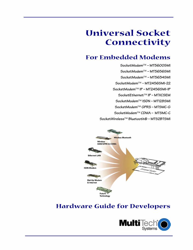
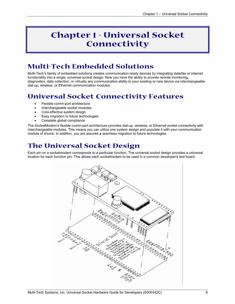
Multi-Tech Embedded Solutions Multi-Tech’s family of embedded solutions creates communication-ready devices by integrating data/fax or Internet functionality into a single, universal socket design. Now you have the ability to provide remote monitoring, diagnostics, data collection, or virtually any communication ability to your existing or new device via interchangeable dial-up, wireless, or Ethernet communication modules.
Universal Socket Connectivity Features • Flexible comm-port architecture • Interchangeable socket modules • Cost-effective system design • Easy migration to future technologies • Complete global compliance
The SocketModem's flexible comm-port architecture provides dial-up, wireless, or Ethernet socket connectivity with interchangeable modules. This means you can utilize one system design and populate it with your communication module of choice. In addition, you are assured a seamless migration to future technologies.
The Universal Socket Design Each pin on a socketmodem corresponds to a particular function. The universal socket design provides a universal location for each function pin. This allows each socketmodem to be used in a common developer's test board.
Chapter 1 – Universal Socket Connectivity
Multi-Tech Systems, Inc. Universal Socket Hardware Guide for Developers (S000342C) 9
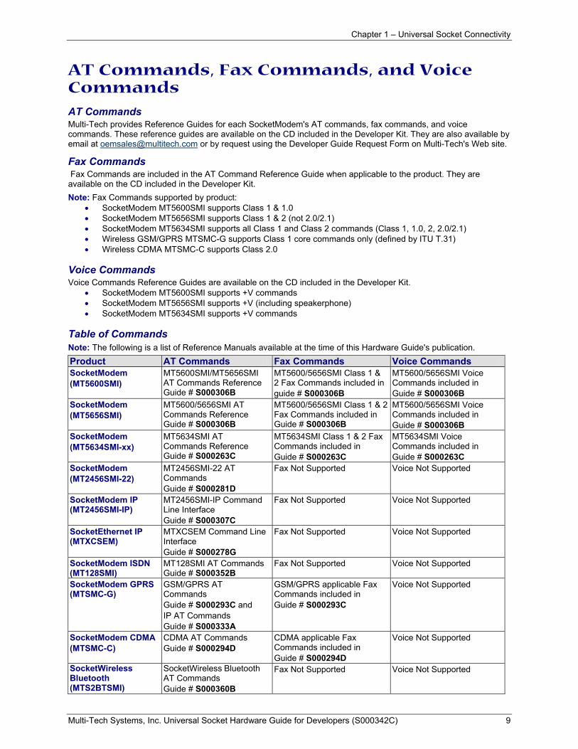
AT Commands, Fax Commands, and Voice Commands
AT Commands Multi-Tech provides Reference Guides for each SocketModem's AT commands, fax commands, and voice commands. These reference guides are available on the CD included in the Developer Kit. They are also available by email at [email protected] or by request using the Developer Guide Request Form on Multi-Tech's Web site.
Fax Commands Fax Commands are included in the AT Command Reference Guide when applicable to the product. They are available on the CD included in the Developer Kit. Note: Fax Commands supported by product:
• SocketModem MT5600SMI supports Class 1 & 1.0 • SocketModem MT5656SMI supports Class 1 & 2 (not 2.0/2.1) • SocketModem MT5634SMI supports all Class 1 and Class 2 commands (Class 1, 1.0, 2, 2.0/2.1) • Wireless GSM/GPRS MTSMC-G supports Class 1 core commands only (defined by ITU T.31) • Wireless CDMA MTSMC-C supports Class 2.0
Voice Commands Voice Commands Reference Guides are available on the CD included in the Developer Kit.
• SocketModem MT5600SMI supports +V commands • SocketModem MT5656SMI supports +V (including speakerphone) • SocketModem MT5634SMI supports +V commands
Table of Commands Note: The following is a list of Reference Manuals available at the time of this Hardware Guide's publication. Product AT Commands Fax Commands Voice Commands SocketModem (MT5600SMI)
MT5600SMI/MT5656SMI AT Commands Reference Guide # S000306B
MT5600/5656SMI Class 1 & 2 Fax Commands included in guide # S000306B
MT5600/5656SMI Voice Commands included in Guide # S000306B
SocketModem (MT5656SMI)
MT5600/5656SMI AT Commands Reference Guide # S000306B
MT5600/5656SMI Class 1 & 2 Fax Commands included in Guide # S000306B
MT5600/5656SMI Voice Commands included in Guide # S000306B
SocketModem (MT5634SMI-xx)
MT5634SMI AT Commands Reference Guide # S000263C
MT5634SMI Class 1 & 2 Fax Commands included in Guide # S000263C
MT5634SMI Voice Commands included in Guide # S000263C
SocketModem (MT2456SMI-22)
MT2456SMI-22 AT Commands Guide # S000281D
Fax Not Supported Voice Not Supported
SocketModem IP (MT2456SMI-IP)
MT2456SMI-IP Command Line Interface Guide # S000307C
Fax Not Supported Voice Not Supported
SocketEthernet IP (MTXCSEM)
MTXCSEM Command Line Interface Guide # S000278G
Fax Not Supported Voice Not Supported
SocketModem ISDN (MT128SMI)
MT128SMI AT Commands Guide # S000352B
Fax Not Supported Voice Not Supported
SocketModem GPRS (MTSMC-G)
GSM/GPRS AT Commands Guide # S000293C and IP AT Commands Guide # S000333A
GSM/GPRS applicable Fax Commands included in Guide # S000293C
Voice Not Supported
SocketModem CDMA (MTSMC-C)
CDMA AT Commands Guide # S000294D
CDMA applicable Fax Commands included in Guide # S000294D
Voice Not Supported
SocketWireless Bluetooth (MTS2BTSMI)
SocketWireless Bluetooth AT Commands Guide # S000360B
Fax Not Supported Voice Not Supported
Chapter 1 – Universal Socket Connectivity
Multi-Tech Systems, Inc. Universal Socket Hardware Guide for Developers (S000342C) 10
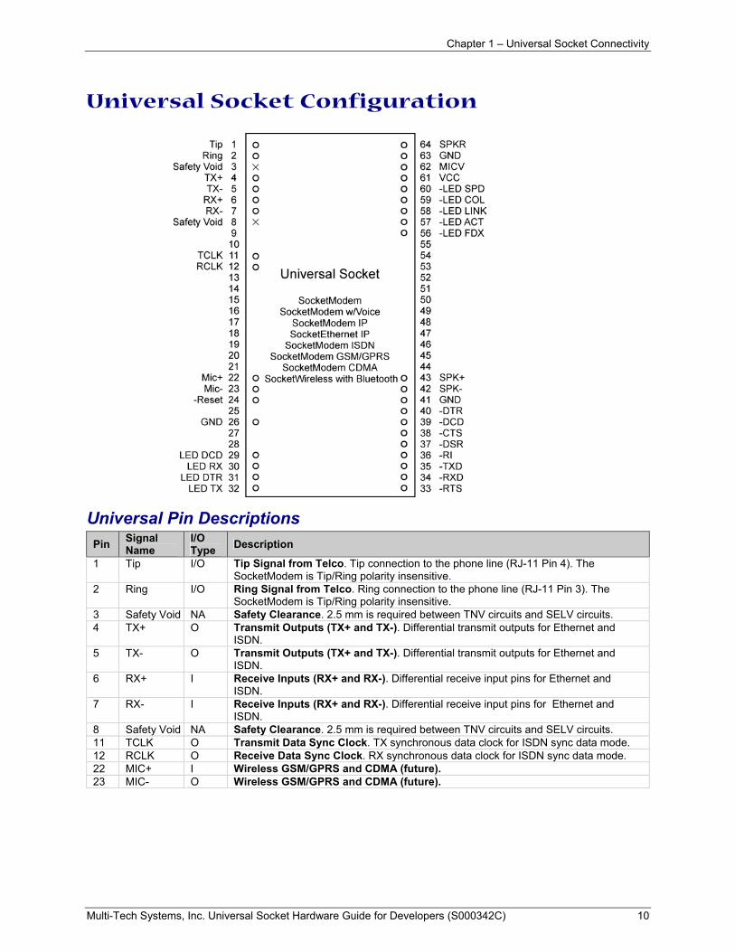
Universal Socket Configuration
Universal Pin Descriptions Pin Signal
Name I/O Type Description
1 Tip I/O Tip Signal from Telco. Tip connection to the phone line (RJ-11 Pin 4). The SocketModem is Tip/Ring polarity insensitive.
2 Ring I/O Ring Signal from Telco. Ring connection to the phone line (RJ-11 Pin 3). The SocketModem is Tip/Ring polarity insensitive.
3 Safety Void NA Safety Clearance. 2.5 mm is required between TNV circuits and SELV circuits. 4 TX+ O Transmit Outputs (TX+ and TX-). Differential transmit outputs for Ethernet and
ISDN. 5 TX- O Transmit Outputs (TX+ and TX-). Differential transmit outputs for Ethernet and
ISDN. 6 RX+ I Receive Inputs (RX+ and RX-). Differential receive input pins for Ethernet and
ISDN. 7 RX- I Receive Inputs (RX+ and RX-). Differential receive input pins for Ethernet and
ISDN. 8 Safety Void NA Safety Clearance. 2.5 mm is required between TNV circuits and SELV circuits. 11 TCLK O Transmit Data Sync Clock. TX synchronous data clock for ISDN sync data mode. 12 RCLK O Receive Data Sync Clock. RX synchronous data clock for ISDN sync data mode. 22 MIC+ I Wireless GSM/GPRS and CDMA (future). 23 MIC- O Wireless GSM/GPRS and CDMA (future).
Chapter 1 – Universal Socket Connectivity
Multi-Tech Systems, Inc. Universal Socket Hardware Guide for Developers (S000342C) 11
Pin Signal Name
I/O Type Description
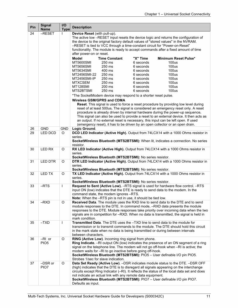
24 –RESET I Device Reset (with pull-up). The active low –RESET input resets the device logic and returns the configuration of the device to the original factory default values of "stored values" in the NVRAM. –RESET is tied to VCC through a time-constant circuit for “Power-on-Reset” functionality. The module is ready to accept commands after a fixed amount of time after power-on or reset. Model Time Constant "X" Time Minimum Reset Pulse* MT5600SMI 250 ms 6 seconds 100us MT5656SMI 250 ms 6 seconds 100us MT5634SMI 400 ms 6 seconds 100us MT2456SMI-22 250 ms 6 seconds 100us MT2456SMI-IP 250 ms 6 seconds 100us MTXCSEM 250 ms 6 seconds 100us MT128SMI 200 ms 6 seconds 100us MTS2BTSMI 250 ms 6 seconds 100us *The SocketModem device may respond to a shorter reset pulse. Wireless GSM/GPRS and CDMA
Reset. This signal is used to force a reset procedure by providing low level during reset of at least 500us. The signal is considered an emergency reset only. A reset procedure is already driven by internal hardware during the power-up sequence. This signal can also be used to provide a reset to an external device. It then acts as an output. If no external reset is necessary, this input can be left open. If used (emergency reset), it has to be driven by an open collector or an open drain.
26 GND GND Logic Ground. 29 LED DCD O DCD LED Indicator (Active High). Output from 74LCX14 with a 1000 Ohms resistor in
series. SocketWireless Bluetooth (MTS2BTSMI): When lit, indicates a connection. No series resistor.
30 LED RX O RX LED Indicator (Active High). Output from 74LCX14 with a 1000 Ohms resistor in series. SocketWireless Bluetooth (MTS2BTSMI): No series resistor.
31 LED DTR O DTR LED Indicator (Active High). Output from 74LCX14 with a 1000 Ohms resistor in series. SocketWireless Bluetooth (MTS2BTSMI): No series resistor.
32 LED TX O TX LED Indicator (Active High). Output from 74LCX14 with a 1000 Ohms resistor in series. SocketWireless Bluetooth (MTS2BTSMI): No series resistor.
33 –RTS I Request to Sent (Active Low). –RTS signal is used for hardware flow control. –RTS input ON (low) indicates that the DTE is ready to send data to the modem. In the command state, the modem ignores –RTS. Note: When the –RTS pin is not in use, it should be tied low.
34 –RXD O Received Data. The module uses the RXD line to send data to the DTE and to send module responses to the DTE. In command mode, –RXD data presents the module responses to the DTE. Module responses take priority over incoming data when the two signals are in competition for –RXD. When no data is transmitted, the signal is held in mark condition.
35 –TXD I Transmitted Data. The DTE uses the –TXD line to send data to the module for transmission or to transmit commands to the module. The DTE should hold this circuit in the mark state when no data is being transmitted or during between intervals between characters.
36 –RI or PIO5
O RING (Active Low). Incoming ring signal from phone. Ring Indicate. –RI output ON (low) indicates the presence of an ON segment of a ring signal on the telephone line. The modem will not go off-hook when –RI is active; the modem waits for –RI to go inactive before going off-hook. SocketWireless Bluetooth (MTS2BTSMI): PIO5 – User definable I/O pin PIO5. Strobes 1/sec for slave indication.
37 –DSR or PIO7
O Data Set Ready (Active Low). –DSR indicates module status to the DTE. –DSR OFF (high) indicates that the DTE is to disregard all signals appearing on the interchange circuits except Ring Indicator (–RI). It reflects the status of the local data set and does not indicate an actual link with any remote data equipment. SocketWireless Bluetooth (MTS2BTSMI): PIO7 – User definable I/O pin PIO7. Defaults as input.
Chapter 1 – Universal Socket Connectivity
Multi-Tech Systems, Inc. Universal Socket Hardware Guide for Developers (S000342C) 12
Pin Signal Name
I/O Type Description
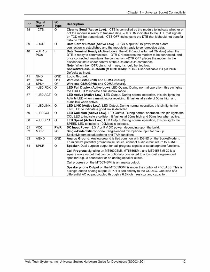
38 –CTS O Clear to Send (Active Low). –CTS is controlled by the module to indicate whether or not the module is ready to transmit data. –CTS ON indicates to the DTE that signals on TXD will be transmitted. –CTS OFF indicates to the DTE that it should not transfer data on TXD.
39 –DCD O Data Carrier Detect (Active Low). –DCD output is ON (low) when a data connection is established and the module is ready to send/receive data.
40 –DTR or PIO6
I Data Terminal Ready (Active Low). The –DTR input is turned ON (low) when the DTE is ready to communicate. –DTR ON prepares the modem to be connected, and, once connected, maintains the connection. –DTR OFF places the modem in the disconnect state under control of the &Dn and &Qn commands. Note: When the –DTR pin is not in use, it should be tied low. SocketWireless Bluetooth (MTS2BTSMI): PIO6 – User definable I/O pin PIO6. Defaults as input.
41 GND GND Logic Ground. 42 SPK- O/O Wireless GSM/GPRS and CDMA (future). 43 SPK+ O/I Wireless GSM/GPRS and CDMA (future). 56 –LED FDX O LED Full Duplex (Active Low). LED Output. During normal operation, this pin lights
the FDX LED to indicate a full duplex mode. 57 –LED ACT O LED Active (Active Low). LED Output. During normal operation, this pin lights the
Activity LED when transmitting or receiving. It flashes at a rate of 50ms high and 50ms low when active.
58 –LEDLINK O LED LINK (Active Low). LED Output. During normal operation, this pin lights the LINK LED to indicate a good link is detected.
59 –LEDCOL O LED Collision (Active Low). LED Output. During normal operation, this pin lights the COL LED to indicate a collision. It flashes at 50ms high and 50ms low when active.
60 –LEDSPD O LED Speed (Active Low). LED Output. During normal operation, this pin lights the SPEED LED to indicate 100Mbps is selected.
61 VCC PWR DC Input Power. 3.3 V or 5 V DC power, depending upon the build. 62 MICV I/O Single-Ended Microphone. Single-ended microphone input for dial-up
SocketModem speakerphone and TAM functions. 63 AGND GND Analog Ground. Analog ground is tied common with DGND on the SocketModem.
To minimize potential ground noise issues, connect audio circuit return to AGND. 64 SPKR O Speaker. Dual purpose output for call progress signals or speakerphone functions.
Call Progress signaling on MT5600SMI, MT5656SMI, and MT2456SMI-22 is a square wave output that can be optionally connected to a low-cost single-ended speaker; e.g., a sounducer or an analog speaker circuit. Call progress on the MT5634SMI is an analog output. Speakerphone Output on the MT5656SMI is under the control of +FCLASS. This is a single-ended analog output. SPKR is tied directly to the CODEC. One side of a differential AC output coupled through a 6.8K ohm resistor and capacitor.
Chapter 1 – Universal Socket Connectivity
Multi-Tech Systems, Inc. Universal Socket Hardware Guide for Developers (S000342C) 13
Design Considerations Good engineering practices must be adhered to when designing a printed circuit board (PCB) containing the SocketModem module. Suppression of noise is essential to the proper operation and performance of the modem itself and for surrounding equipment.
Two aspects of noise in an OEM board design containing the SocketModem must be considered: on-board/off-board generated noise that can affect digital signal processing. Both on-board and off-board generated noise that is coupled on-board can affect interface signal levels and quality. Of particular concern is noise in frequency ranges affecting modem performance.
On-board generated electromagnetic interference (EMI) noise that can be radiated or conducted off-board is a separate, but equally important, concern. This type of noise can affect the operation of surrounding equipment. Most local government agencies have stringent certification requirements that must be met for use in specific environments.
Proper PC board layout (component placement, signal routing, trace thickness and geometry, etc.) component selection (composition, value, and tolerance), interface connections, and shielding are required for the board design to achieve desired modem performance and to attain EMI certification.
The aspects of proper engineering practices are beyond the scope of this designer guide. The designer should consult noise suppression techniques described in technical publications and journals, electronics and electrical engineering text books, and component supplier application notes.
PC Board Layout Guidelines In a 4-layer design, provide adequate ground plane covering the entire board. In 4-layer designs, power and ground are typically on the inner layers. All power and ground traces should be 0.05 inches wide.
The recommended hole size for the SocketModem pins is 0.036 in. +/-0.003 in. in diameter. Spacers can be used to hold the SocketModem vertically in place during the wave solder process. A spacer should be placed on pin 32 and pin 64 of the SocketModem. A suggested part number for the spacer is BIVAR 938-0.130 for P1 (0.310in) option SocketModems. The spacers can be left on permanently and will not effect operation.
All creepages and clearances for the SocketModem have been designed to meet requirements of safety standards EN60950. The requirements are based on a working voltage of 250V. When the recommended DAA circuit interface is implemented in a third party design all creepage and clearance requirements must be strictly adhered to. The third party safety design must be evaluated by the appropriate national agency per the required specification.
User accessible areas: Based on where the third party design is to be marketed, sold, or used, it may be necessary to provide an insulating cover over all TNV exposed areas. Consult with the recognized safety agency to determine the requirements.
Note: Even if the recommended design considerations are followed, there are no guarantees that a particular system will comply with all the necessary regulatory requirements. It is imperative that specific designs be completely evaluated by a qualified/recognized agency.
Chapter 1 – Universal Socket Connectivity
Multi-Tech Systems, Inc. Universal Socket Hardware Guide for Developers (S000342C) 14
Electromagnetic Interference (EMI) Considerations The following guidelines are offered to specifically help minimize EMI generation. Some of these guidelines are the same as, or similar to, the general guidelines but are mentioned again to reinforce their importance. In order to minimize the contribution of the SocketModem-based design to EMI, the designer must understand the major sources of EMI and how to reduce them to acceptable levels.
1. Keep traces carrying high frequency signals as short as possible.
2. Provide a good ground plane or grid. In some cases, a multilayer board may be required with full layers for ground and power distribution.
3. Decouple power from ground with decoupling capacitors as close to the SocketModem module power pins as possible.
4. Eliminate ground loops, which are unexpected current return paths to the power source and ground.
5. Decouple the telephone line cables at the telephone line jacks. Typically, use a combination of series inductors, common mode chokes, and shunt capacitors. Methods to decouple telephone lines are similar to decoupling power lines; however, telephone line decoupling may be more difficult and deserves additional attention. A commonly used design aid is to place footprints for these components and populate as necessary during performance/EMI testing and certification.
6. Decouple the power cord at the power cord interface with decoupling capacitors. Methods to decouple power lines are similar to decoupling telephone lines.
7. Locate high frequency circuits in a separate area to minimize capacitive coupling to other circuits.
8. Locate cables and connectors so as to avoid coupling from high frequency circuits.
9. Lay out the highest frequency signal traces next to the ground grid.
10. If a multilayer board design is used, make no cuts in the ground or power planes and be sure the ground plane covers all traces.
11. Minimize the number of through-hole connections on traces carrying high frequency signals.
12. Avoid right angle turns on high frequency traces. Forty-five degree corners are good; however, radius turns are better.
13. On 2-layer boards with no ground grid, provide a shadow ground trace on the opposite side of the board to traces carrying high frequency signals. This will be effective as a high frequency ground return if it is three times the width of the signal traces.
14. Distribute high frequency signals continuously on a single trace rather than several traces radiating from one point.
Chapter 1 – Universal Socket Connectivity
Multi-Tech Systems, Inc. Universal Socket Hardware Guide for Developers (S000342C) 15
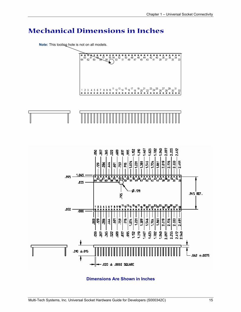
Mechanical Dimensions in Inches
Note: This tooling hole is not on all models.
1 2 3 4 5 6 7 8 9 10 11 12 13 14 15 16 1718
1920
2122
23 24 2526
2728
2930
3132
6463
6261
6059
5857
5655 54
5352
5150
4948
4746
4544
4342
4140
3938
3736
3534
33
Dimensions Are Shown in Inches
Chapter 1 – Universal Socket Connectivity
Multi-Tech Systems, Inc. Universal Socket Hardware Guide for Developers (S000342C) 16
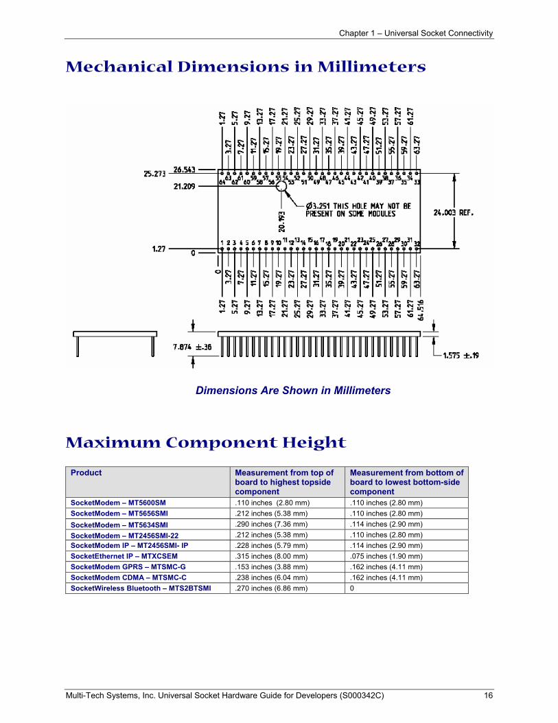
Mechanical Dimensions in Millimeters
Dimensions Are Shown in Millimeters
Maximum Component Height
Product Measurement from top of board to highest topside component
Measurement from bottom of board to lowest bottom-side component
SocketModem – MT5600SM .110 inches (2.80 mm) .110 inches (2.80 mm) SocketModem – MT5656SMI .212 inches (5.38 mm) .110 inches (2.80 mm) SocketModem – MT5634SMI .290 inches (7.36 mm) .114 inches (2.90 mm) SocketModem – MT2456SMI-22 .212 inches (5.38 mm) .110 inches (2.80 mm) SocketModem IP – MT2456SMI- IP .228 inches (5.79 mm) .114 inches (2.90 mm) SocketEthernet IP – MTXCSEM .315 inches (8.00 mm) .075 inches (1.90 mm) SocketModem GPRS – MTSMC-G .153 inches (3.88 mm) .162 inches (4.11 mm) SocketModem CDMA – MTSMC-C .238 inches (6.04 mm) .162 inches (4.11 mm) SocketWireless Bluetooth – MTS2BTSMI .270 inches (6.86 mm) 0
Chapter 1 – Universal Socket Connectivity
Multi-Tech Systems, Inc. Universal Socket Hardware Guide for Developers (S000342C) 17
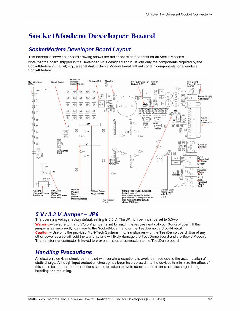
SocketModem Developer Board
SocketModem Developer Board Layout This theoretical developer board drawing shows the major board components for all SocketModems. Note that the board shipped in the Developer Kit is designed and built with only the components required by the SocketModem in that kit; e.g., a serial dialup SocketModem board will not contain components for a wireless SocketModem.
5 V / 3.3 V Jumper – JP6 The operating voltage factory default setting is 3.3 V. The JP1 jumper must be set to 3.3-volt. Warning – Be sure to that 5 V/3.3 V jumper is set to match the requirements of your SocketModem. If this jumper is set incorrectly, damage to the SocketModem and/or the Test/Demo card could result. Caution – Use only the provided Multi-Tech Systems, Inc. transformer with the Test/Demo board. Use of any other power source will void the warranty and will likely damage the Test/Demo board and the SocketModem. The transformer connector is keyed to prevent improper connection to the Test/Demo board.
Handling Precautions All electronic devices should be handled with certain precautions to avoid damage due to the accumulation of static charge. Although input protection circuitry has been incorporated into the devices to minimize the effect of this static buildup, proper precautions should be taken to avoid exposure to electrostatic discharge during handling and mounting.
Chapter 1 – Universal Socket Connectivity
Multi-Tech Systems, Inc. Universal Socket Hardware Guide for Developers (S000342C) 18
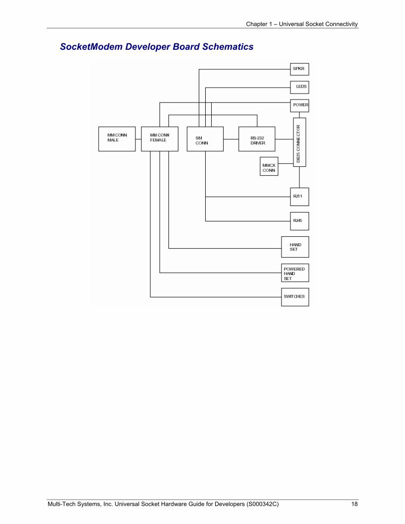
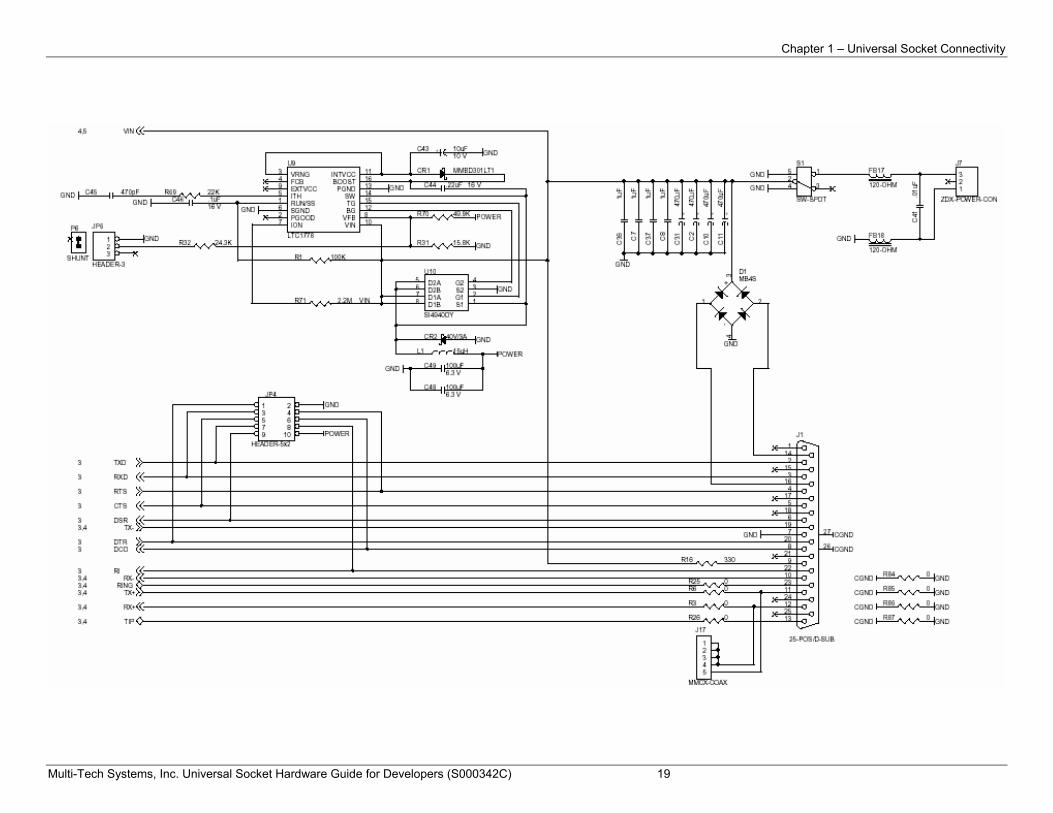
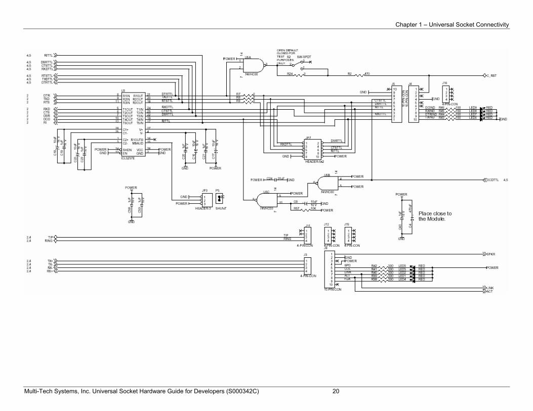
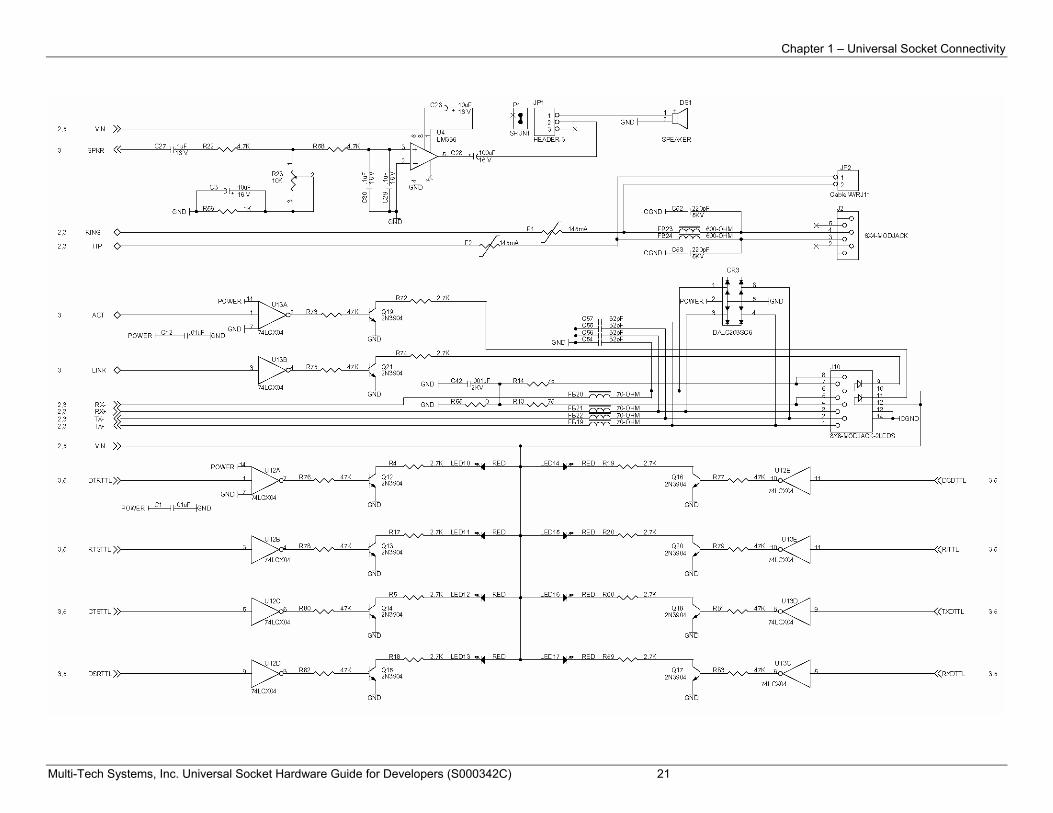
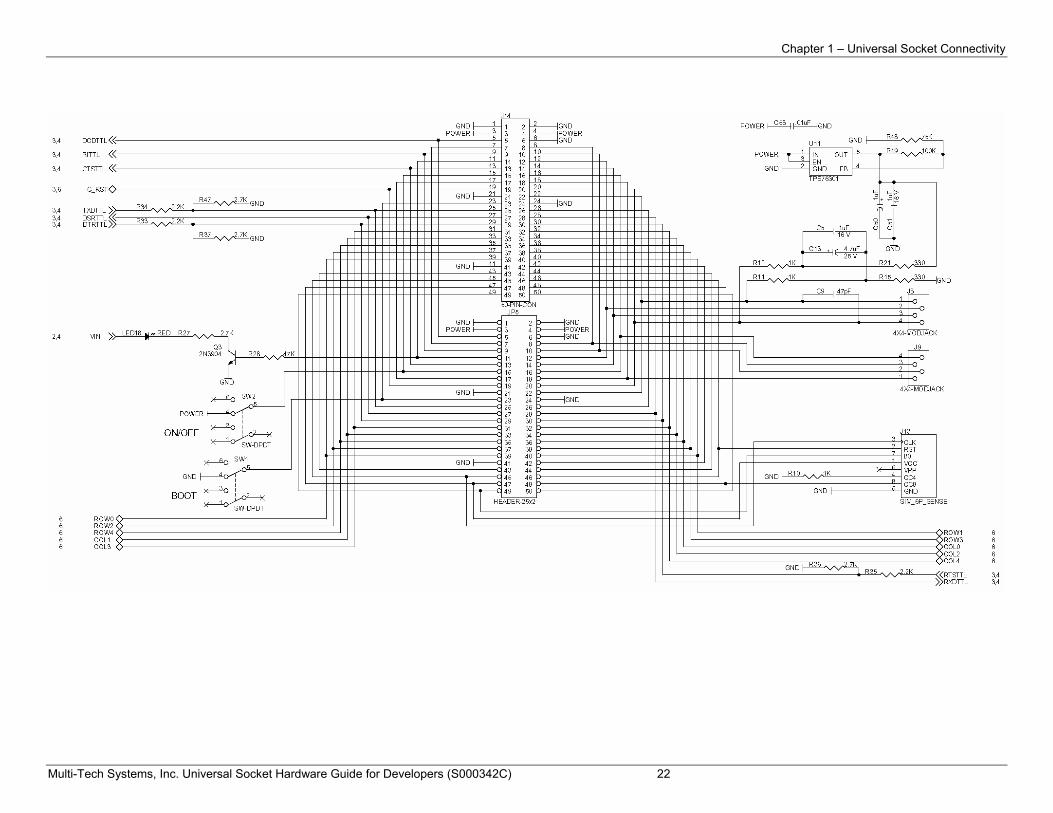
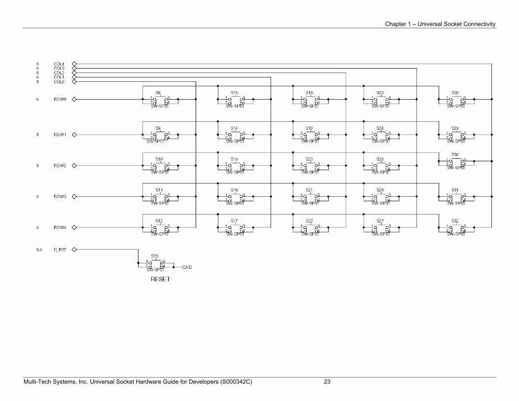
SocketModem Developer Board Schematics
Chapter 1 – Universal Socket Connectivity
Multi-Tech Systems, Inc. Universal Socket Hardware Guide for Developers (S000342C) 19
Chapter 1 – Universal Socket Connectivity
Multi-Tech Systems, Inc. Universal Socket Hardware Guide for Developers (S000342C) 20
Chapter 1 – Universal Socket Connectivity
Multi-Tech Systems, Inc. Universal Socket Hardware Guide for Developers (S000342C) 21
Chapter 1 – Universal Socket Connectivity
Multi-Tech Systems, Inc. Universal Socket Hardware Guide for Developers (S000342C) 22
Chapter 1 – Universal Socket Connectivity
Multi-Tech Systems, Inc. Universal Socket Hardware Guide for Developers (S000342C) 23
Chapter 1 – Universal Socket Connectivity
Multi-Tech Systems, Inc. Universal Socket Hardware Guide for Developers (S000342C) 24
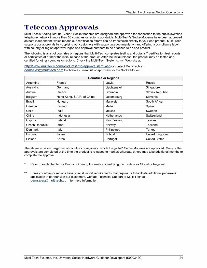
Telecom Approvals Multi-Tech's Analog Dial-up Global* SocketModems are designed and approved for connection to the public switched telephone network in more than 50 countries or regions worldwide. Multi-Tech's SocketModems have been approved as host independent, which means our certification efforts can be transferred directly to your end product. Multi-Tech supports our approvals by supplying our customers with supporting documentation and offering a compliance label with country or region approval logos and approval numbers to be attached to an end product.
The following is a list of countries or regions that Multi-Tech completes testing and obtains** certification test reports or certificates at or near the initial release of the product. After the initial release, the product may be tested and certified for other countries or regions. Check the Multi-Tech Systems, Inc. Web site at
http://www.multitech.com/products/info/approvals/smi.asp or contact Multi-Tech at [email protected] to obtain a current list of approvals for the SocketModem.
Countries or Regions Argentina France Latvia Russia Australia Germany Liechtenstein Singapore Austria Greece Lithuania Slovak Republic Belgium Hong Kong, S.A.R. of China Luxembourg Slovenia Brazil Hungary Malaysia South Africa Canada Iceland Malta Spain Chile India Mexico Sweden China Indonesia Netherlands Switzerland Cyprus Ireland New Zealand Taiwan Czech Republic Israel Norway Thailand Denmark Italy Philippines Turkey Estonia Japan Poland United Kingdom Finland Korea Portugal United States
The above list is our target set of countries or regions in which the global* SocketModems are approved. Many of the approvals are completed at the time the product is released to market; whereas, others may take additional months to complete the approval. * Refer to each chapter for Product Ordering Information identifying the modem as Global or Regional. ** Some countries or regions have special import requirements that require us to facilitate additional paperwork
application in partner with our customers. Contact Technical Support or Multi-Tech at [email protected] for more information.
Chapter 1 – Universal Socket Connectivity
Multi-Tech Systems, Inc. Universal Socket Hardware Guide for Developers (S000342C) 25
United States Labeling Requirements Note: Telecom does not apply to all products. For example, this not applicable for the Wireless GSM/GPRS and CDMA products. Approved terminal equipment and approved protective circuitry shall prominently display the following information using the format shown below:
• Responsible party • Product Identification • Equipment Code • Ringer Equivalence • Ringer Type • Indication that the product meets the requirements of FCC Part 68
The information required by the first five items shall correspond to the records in the ACTA (America's Carriers Telecommunications Association) database of approved equipment. The required information shall be encoded in the following format: US: AAAEQ##TXXX Where:
US: Is a fixed field that indicates the equipment meets all requirements of 47 CFR Part 68, including the requirements published by ACTA (America's Carriers Telecommunications Association).
AAA is the responsible party’s Grantee Code obtained previously from the FCC’s Common Carrier Bureau or currently from ACTA. EQ Is an Equipment Code indicating to the Service Provider any special signal handling or billing requirements. The Equipment codes are listed in Annex A (normative). ## is the Ringer Equivalence Number without a decimal point (e.g. REN of 1.0 = 10, REN of 0.3 = 03). In the case of a “Z” ringer, ZZ shall appear. In the case of approved equipment without a network interface and equipment not connecting to circuits with analog ringing supplied then “NA” shall appear. T is the ringer type letter associated with the Ringer Equivalence Number, in accordance with the technical requirements. In the case of approved equipment without a network interface and equipment not connecting to circuits with analog ringing supplied, the letter “N” shall appear. XXX Is a product identifier, unique when combined with the responsible party’s Grantee Code, of at least one and up to nine alphanumeric characters (including one or more dashes (-) if desired. A dash shall not appear as the first or last character nor shall the identifier consist entirely of dashes). The responsible party shall define this identifier.
Label Physical Characteristics The information required above shall be permanently affixed and legible without magnification. It may be etched, engraved, stamped, indelibly printed or otherwise permanently marked. Alternatively, the required information may be permanently marked on a nameplate of metal, plastic or other material fastened to the enclosure by welding, riveting or with a permanent adhesive. Such a nameplate shall be able to last for the expected lifetime of the equipment and shall not be readily detachable.
Labeling Continuity and Changes The labeling content and format requirements in effect when a product was approved shall be effective for the life of the product. The labeling content and format requirements in effect at approval shall also continue to be effective for modified products. However, the responsible party shall have the option of conforming a product's labeling to current content and format requirements at any time.
Other Label Requirements The label shall be placed in one of the following locations in a location where it can be found after installation:
• on an outside surface • inside a readily available access door or panel • on another readily accessible surface
For example, the label should not be placed on the rear of a permanently wall-mounted device in a manner such that it is not readily accessible.
Chapter 1 – Universal Socket Connectivity
Multi-Tech Systems, Inc. Universal Socket Hardware Guide for Developers (S000342C) 26
Canadian Labeling Requirements The following requirements are established under section 69.3 of the Telecommunications Act for purposes of section 5 of the Telecommunications Apparatus Regulations. Registered equipment shall bear the following identifying marks, and the Declaring Party shall ensure that these marks are permanently affixed to the equipment:
(a) The registration number — Specifications of this mark are given in the document: Self-Marking of the Certification/Registration Number on Terminal Equipment — Application Procedure and Agreement; and
(b) The model identification number under which the product was registered. A statement of compliance with Industry Canada requirements, such as the one given below, shall accompany each unit of equipment whether registered under this procedure or previously certified: "This product meets the applicable Industry Canada technical specifications" For terminal equipment intended for connection to loop-start or ground-start interfaces, the Ringer Equivalence Number (REN) must be calculated as per Section 1.8 of CS-03, Part I. A REN higher than that determined may be assigned by manufacturers to allow for production variations. The REN must be marked on the terminal equipment itself or added to the note below. A note similar to the following shall accompany each unit of equipment whether registered under this procedure or previously certified: "The Ringer Equivalence Number is an indication of the maximum number of devices allowed to be connected to a telephone interface. The termination on an interface may consist of any combination of devices subject only to the requirement that the sum of the RENs of all the devices does not exceed five". Pursuant to section 69.3 of the Telecommunications Act, Certified or self-declared TE will bear a valid identifying certification or registration number. The marking of the certification or registration number on the product shall be as follows:
(a) TAC holder/DP will be responsible for permanently affixing the certification/registration number on the TE. The certification/registration number (see example below) identifies Certified or self-declared TE to the public, representatives of the telecommunications common carriers, the Department, and other interested parties. The letter height must be no less than 1.5 mm and the letters must be legible without magnification.
(b) For integrated devices, e.g. a modem or one that is intended to become a sub-assembly of host equipment e.g. a data terminal, computer etc. that are designed to interface directly with the network, the certification/registration number shall be affixed to the integrated device itself.
(c) The certification/registration number for a packaged TE will denote that the total package has been registered. However, the marking will normally be placed on that unit of the package which connects to the network; e.g., in a PBX the marking will be placed on the common equipment which connects to the network, rather than on plug-in components which may be added later. The Terminal Equipment List will show the common equipment but not the standard station apparatus or any proprietary station apparatus.
(d) The marking format of the certification/registration number is as follows: IC: XXXXXX-YYYYYYYY Where:
• The letters "IC" have no other meaning or purpose than to identify the Industry Canada certification/registration number, and
• “XXXXXX-YYYYYYYY” is the certification/registration number; “XXXXXX” is the Company Number¹ (CN); it consists of up to six alphanumeric characters (A-Z, 0-9) assigned by Industry Canada; and “YYYYYYYY” is the Unique Product Number (UPN); it consists of up to eight alphanumeric characters (A-Z, 0-9) assigned by the applicant. Other characters, (such as & # *-) may not be used. Alphabetic characters must be capitalized.
¹ Note: The Company Number of registered equipment ends with an alphabetic character. (e) Certification Numbers granted prior to the implementation of the above marking format are
grandfathered. (i) For previously certified TE, the self-marking format shall consist of the old certification number
preceded by “IC:” For example, if the certification number is “123 1234 A”, then the self-mark would read “IC: 123 1234 A”.
(ii) For a new model that is registered to a family of previously certified TE, the self-marking format shall be: IC: XXXXXX-ZZZZZZZZ Where:
Chapter 1 – Universal Socket Connectivity
Multi-Tech Systems, Inc. Universal Socket Hardware Guide for Developers (S000342C) 27
• “XXXXXX” is the Company Number, as in (d) above; and
• “ZZZZZZZZ” is either the old certification number minus the old company number, or a new Unique Product Number assigned by the applicant. For example, if a new model is registered to the family of products with certification number “123 1234 A”, and that the Company Number for the registration is “123A”, then the self-mark for this new model would read “IC: 123A-1234 A”. If the applicant decides to replace “1234 A” with a new UPN, say “5678", then the self-mark would read “IC: 123A-5678".
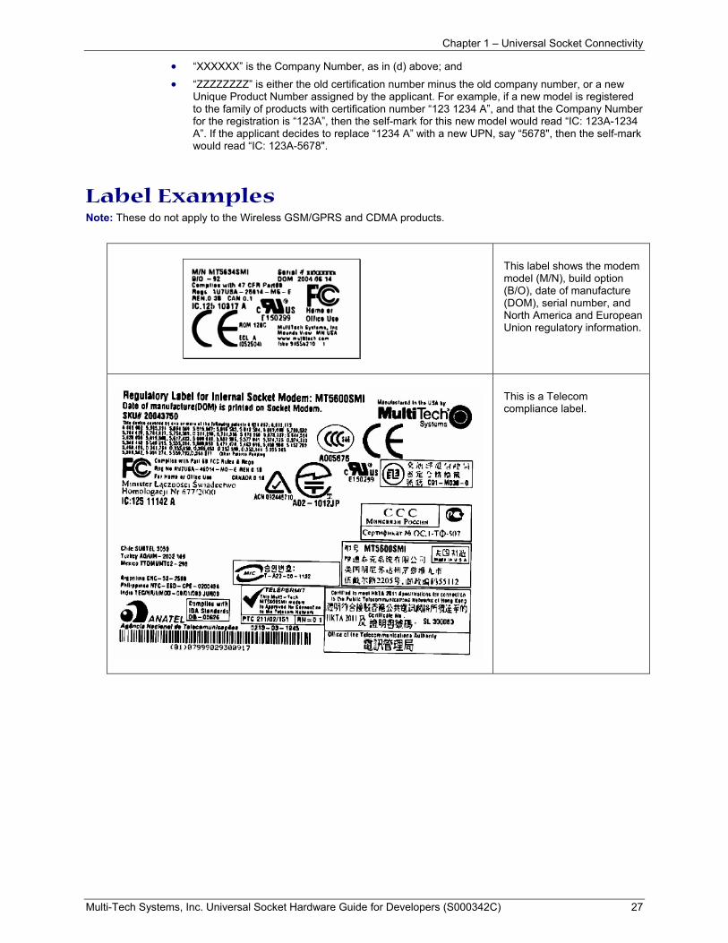
Label Examples Note: These do not apply to the Wireless GSM/GPRS and CDMA products.
This label shows the modem model (M/N), build option (B/O), date of manufacture (DOM), serial number, and North America and European Union regulatory information.
This is a Telecom compliance label.
Chapter 1 – Universal Socket Connectivity
Multi-Tech Systems, Inc. Universal Socket Hardware Guide for Developers (S000342C) 28
Regulatory Compliance Statements
EMC, Safety, and R&TTE Directive Compliance The CE mark is affixed to this product to confirm compliance with the following European Community Directives:
Council Directive 89/336/EEC of 3 May 1989 on the approximation of the laws of Member States relating to electromagnetic compatibility; and Council Directive 73/23/EEC of 19 February 1973 on the harmonization of the laws of Member States relating to electrical equipment designed for use within certain voltage limits; and Council Directive 1999/5/EC of 9 March on radio equipment and telecommunications terminal equipment and the mutual recognition of their conformity.
International Modem Restrictions Some dialing and answering defaults and restrictions may vary for international modems. Changing settings may cause a modem to become non-compliant with national telecom requirements in specific countries. Also note that some software packages may have features or lack restrictions that may cause the modem to become non-compliant.
Telecom Requirements for the United States FCC Part 15 Regulation This equipment has been tested and found to comply with the limits for a Class B digital device, pursuant to Part 15 of the FCC rules. These limits are designed to provide reasonable protection against harmful interference in a residential installation. This equipment generates, uses, and can radiate radio frequency energy, and if not installed and used in accordance with the instructions, may cause harmful interference to radio communications. However, there is no guarantee that interference will not occur in a particular installation. If this equipment does cause harmful interference to radio or television reception, which can be determined by turning the equipment off and on, the user is encouraged to try to correct the interference by one or more of the following measures:
Reorient or relocate the receiving antenna. Increase the separation between the equipment and receiver. Plug the equipment into an outlet on a circuit that is different from the one used by the receiver. Consult the dealer or an experienced radio/TV technician for help.
This device complies with Part 15 of the FCC rules. Operation of this device is subject to the following conditions: (1) This device may not cause harmful interference, and (2) this device must accept any interference that may cause undesired operation. WARNING – Changes or modifications to this unit not expressly approved by the party responsible for compliance could void the user’s authority to operate the equipment.
Industry Canada This Class B digital apparatus meets all requirements of the Canadian Interference-Causing Equipment Regulations. Cet appareil numérique de la classe B respecte toutes les exigences du Reglement Canadien sur le matériel brouilleur.
Chapter 1 – Universal Socket Connectivity
Multi-Tech Systems, Inc. Universal Socket Hardware Guide for Developers (S000342C) 29
New Zealand Telecom Warning Notice 1. The grant of a Telepermit for any item of terminal equipment indicates only that Telecom has
accepted that the item complies with minimum conditions for connection to its network. It indicates no endorsement of the product by Telecom, nor does it provide any sort of warranty. Above all, it provides no assurance that any item will work correctly in all respects with another item of Telepermitted equipment of a different make or model, nor does it imply that any product is compatible with all of Telecom’s network services.
This equipment is not capable under all operating conditions of correct operating conditions of correct operation at the higher speed which it is designated. 33.6 kbps and 56 kbps connections are likely to be restricted to lower bit rates when connected to some PSTN implementations. Telecom will accept no responsibility should difficulties arise in such circumstances.
2. Immediately disconnect this equipment should it become physically damaged, and arrange for its disposal or repair.
3. This modem shall not be used in any manner which could constitute a nuisance to other Telecom customers.
4. This device is equipped with pulse dialing, while the Telecom standard is DTMF tone dialing. There is no guarantee that Telecom lines will always continue to support pulse dialing.
Use of pulse dialing, when this equipment is connected to the same line as other equipment, may give rise to 'bell tinkle' or noise and may also cause a false answer condition. Should such problems occur, the user should NOT contact the Telecom Faults Service.
The preferred method of dialing is to use DTMF tones, as this is faster than pulse (decadic) dialing and is readily available on almost all New Zealand telephone exchanges.
5. Warning Notice: No '111' or other calls can be made from this device during a mains power failure. 6. This equipment may not provide for the effective hand-over of a call to another device connected to
the same line. 7. Some parameters required for compliance with Telecom’s Telepermit requirements are dependent
on the equipment (PC) associated with this device. The associated equipment shall be set to operate within the following limits for compliance with Telecom’s Specifications:
For repeat calls to the same number: • There shall be no more than 10 call attempts to the same number within any 30 minute
period for any single manual call initiation, and • The equipment shall go on-hook for a period of not less than 30 seconds between the end
of one attempt and the beginning of the next attempt. For automatic calls to different numbers:
• The equipment shall be set to ensure that automatic calls to different numbers are spaced such that there is no less than 5 seconds between the end of one call attempt and the beginning of another.
8. For correct operation, total of the RN’s of all devices connected to a single line at any time should not exceed 5.
South African Statement This modem must be used in conjunction with an approved surge protection device.
Other The above country-specific examples do not cover all countries with specific regulations; they are included to show you how each country may differ. If you have trouble determining your own country's requirements, check with Multi-Tech's Technical Support for assistance.
Chapter 1 – Universal Socket Connectivity
Multi-Tech Systems, Inc. Universal Socket Hardware Guide for Developers (S000342C) 30
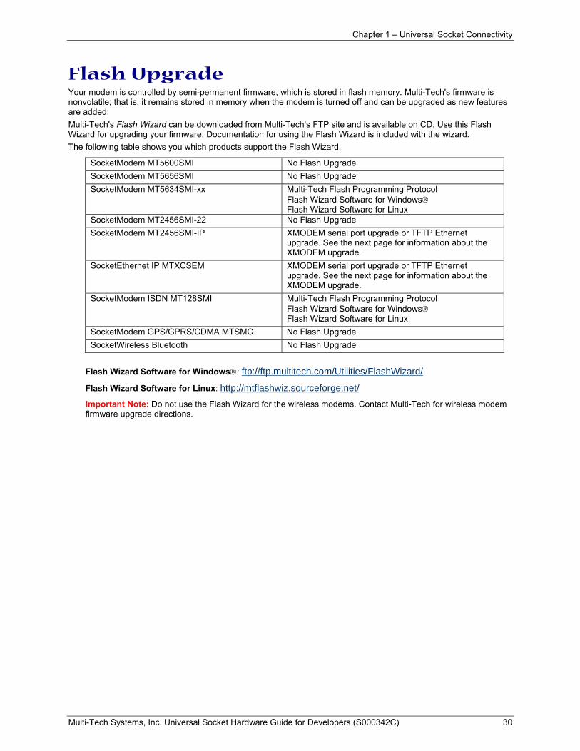
Flash Upgrade Your modem is controlled by semi-permanent firmware, which is stored in flash memory. Multi-Tech's firmware is nonvolatile; that is, it remains stored in memory when the modem is turned off and can be upgraded as new features are added. Multi-Tech's Flash Wizard can be downloaded from Multi-Tech’s FTP site and is available on CD. Use this Flash Wizard for upgrading your firmware. Documentation for using the Flash Wizard is included with the wizard. The following table shows you which products support the Flash Wizard.
SocketModem MT5600SMI No Flash Upgrade SocketModem MT5656SMI No Flash Upgrade SocketModem MT5634SMI-xx Multi-Tech Flash Programming Protocol
Flash Wizard Software for Windows Flash Wizard Software for Linux
SocketModem MT2456SMI-22 No Flash Upgrade SocketModem MT2456SMI-IP XMODEM serial port upgrade or TFTP Ethernet
upgrade. See the next page for information about the XMODEM upgrade.
SocketEthernet IP MTXCSEM XMODEM serial port upgrade or TFTP Ethernet upgrade. See the next page for information about the XMODEM upgrade.
SocketModem ISDN MT128SMI Multi-Tech Flash Programming Protocol Flash Wizard Software for Windows Flash Wizard Software for Linux
SocketModem GPS/GPRS/CDMA MTSMC No Flash Upgrade SocketWireless Bluetooth No Flash Upgrade
Flash Wizard Software for Windows: ftp://ftp.multitech.com/Utilities/FlashWizard/
Flash Wizard Software for Linux: http://mtflashwiz.sourceforge.net/
Important Note: Do not use the Flash Wizard for the wireless modems. Contact Multi-Tech for wireless modem firmware upgrade directions.
Chapter 1 – Universal Socket Connectivity
Multi-Tech Systems, Inc. Universal Socket Hardware Guide for Developers (S000342C) 31
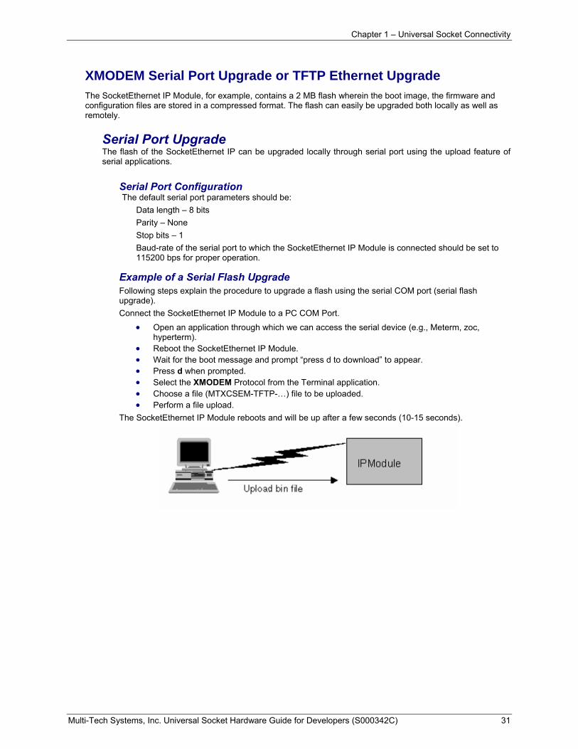
XMODEM Serial Port Upgrade or TFTP Ethernet Upgrade The SocketEthernet IP Module, for example, contains a 2 MB flash wherein the boot image, the firmware and configuration files are stored in a compressed format. The flash can easily be upgraded both locally as well as remotely.
Serial Port Upgrade The flash of the SocketEthernet IP can be upgraded locally through serial port using the upload feature of serial applications.
Serial Port Configuration The default serial port parameters should be:
Data length – 8 bits Parity – None Stop bits – 1 Baud-rate of the serial port to which the SocketEthernet IP Module is connected should be set to 115200 bps for proper operation.
Example of a Serial Flash Upgrade Following steps explain the procedure to upgrade a flash using the serial COM port (serial flash upgrade). Connect the SocketEthernet IP Module to a PC COM Port.
• Open an application through which we can access the serial device (e.g., Meterm, zoc, hyperterm).
• Reboot the SocketEthernet IP Module. • Wait for the boot message and prompt “press d to download” to appear. • Press d when prompted. • Select the XMODEM Protocol from the Terminal application. • Choose a file (MTXCSEM-TFTP-…) file to be uploaded. • Perform a file upload.
The SocketEthernet IP Module reboots and will be up after a few seconds (10-15 seconds).
Chapter 1 – Universal Socket Connectivity
Multi-Tech Systems, Inc. Universal Socket Hardware Guide for Developers (S000342C) 32
Ethernet Port Upgrade The flash can be upgraded remotely through the Ethernet using TFTP. The SocketEthernet IP Module flash contains two main files, which are required for an upgrade.
1. Binary File The binary file contains the firmware of the Module. The name of this binary file would be in the following format. MTXCSEM-TFTP-v<version>w-<date in ddMmmyyyy format>
2. Gun-zipped http.tar.gz File This contains the HTML pages of the serial device and other files related to it, such as http-host-param (http page configuration file). The name of this tar file would always be http.tar.gz
Enabling TFTP Server Enable TFTP server on SocketEthernet IP Module by issuing the following command:
# set ip tftp enable OK
Example of an Ethernet Flash Upgrade The IP module can be remotely upgraded over a network. Make sure a TFTP client is already installed on the machine. The following steps explain the method to perform flash upgrade from Ethernet.
• Make sure the SocketEthernet IP Module is reachable on the LAN. • Perform a TFTP to the SocketEthernet IP Module from a TFTP client.
– Set binary mode ON. Note: This step is very important. – Binary
• Put the binary file. – put <binary filename>
• Exit the TFTP session. – Quit
The SocketEthernet IP Module reboots after it has been successfully upgraded.

Chapter 1 – Universal Socket Connectivity
Multi-Tech Systems, Inc. Universal Socket Hardware Guide for Developers (S000342C) 33
Multi-Tech Systems, Inc. Flash Programming Protocol This information is provided exclusively for the users of Multi-Tech Systems, Inc. modems. Such users Multi-Tech Systems, Inc. modem owners have the right to use, modify, and incorporate this code into other products provided they include the Multi-Tech Systems, Inc. notice and the associated copyright notice with any such product.
Copyright (C) Multi-Tech Systems, Inc. 1995 All Right Reserved
The flash programming protocol is provided "AS IS” without warranty. Important: When interacting with the boot code, it is possible to make the modem inoperable.
Use extreme caution.
Programming the Modem There are two ways to start flash programming a modem. It can be programmed
1. From “AT” mode 2. When the modem powers up.
The following table shows how a modem is programmed. DTE Modem Comments AT*FS\r This effectively “restarts” the modem so that it enters the boot code. Handshake Sequence
M’s Many M’s are sent (10 milliseconds apart) at 19200 baud. This is where the handshake starts if the modem is just powered up.
U U is sent at 19200 baud if M’s are received within 100 milliseconds of power up. If the M’s are not received within 100 milliseconds, then the modem starts up normally. If the AT*FS command is used, then you have 1 second (1000mS) to perform the handshake.
D Sent at 19200 baud. M M if can receive at 9600/19200/38400/57600/115200 I|J|K|L|M I if modem will be programmed at 9600
J if modem will be programmed at 19200 K if modem will be programmed at 38400 L if modem will be programmed at 57600 M if modem will be programmed at 115200
\r\nOK\r\n Modem is ready to be programmed Program Sequence: DTE Modem Comments ATFLP\r Request to the modem to program G Modem is ready for next program packet [Length High] High byte of data packet length [Length Low] Low byte of data packet length
Packet lengths can be up to 4096 bytes in size for most boot code versions
[Address High] High byte of program address [Address Middle] Middle byte of program address [Address Low] Low byte of program address
Addresses are 3 byte values with a range of 00000h-FFFFFh [Data Bytes] These are the data bytes to be programmed at the address specified
above. They must be the same number of bytes as specified above. [Checksum] This checksum is generated by exclusive ORing together all of the
Data Bytes (do not include the Length or Address bytes in that calculation).
\nOK\r\n \nERROR\r\n
If bytes are programmed and verified. If verify fails or checksum is bad. Retry the block 3 times on an ERROR.
….
….
More of the above sequence until all the data bytes have been sent to the modem.
ATFLEND\r This ends programming and restarts the modem.
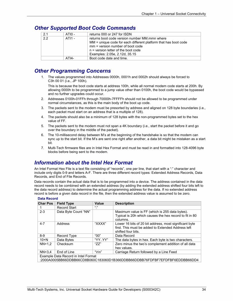
Chapter 1 – Universal Socket Connectivity
Multi-Tech Systems, Inc. Universal Socket Hardware Guide for Developers (S000342C) 34
Other Supported Boot Code Commands 2.1 ATI0 - returns 000 or 247 for ISDN 2.2 ATI1 - returns boot code version number MM.mmn where
MM = unique code for each different platform that has boot code mm = version number of boot code n = version letter of the boot code Examples: 2.05e, 2.12d, 35.15
ATI4- Boot code date and time.
Other Programming Concerns 1. The values programmed into Addresses 0000h, 0001h and 0002h should always be forced to C3h 00 01 (i.e., JP 100h). This is because the boot code starts at address 100h, while all normal modem code starts at 200h. By
allowing 0000h to be programmed to a jump value other than 0100h, the boot code would be bypassed and no further upgrades could occur.
2. Addresses 0100h-01FFh through 70000h-7FFFFh should not be allowed to be programmed under normal circumstances, as this is the main body of the boot up code.
3. The packets sent to the modem must be presorted by address and aligned on 128 byte boundaries (i.e., each packet must start on an address that is a multiple of 128).
4. The packets should also be a minimum of 128 bytes with the non-programmed bytes set to the hex value of FF.
5. The packets sent to the modem must not span a 4K boundary (i.e., start the packet before it and go over the boundary in the middle of the packet).
6. The 10-millisecond delay between M’s at the beginning of the handshake is so that the modem can sync up to the start bit. If the M’s are sent one right after another, a data bit might be mistaken as a start bit.
7. Multi-Tech firmware files are in Intel Hex Format and must be read in and formatted into 128-4096 byte blocks before being sent to the modem.
Information about the Intel Hex Format An Intel Format Hex File is a text file consisting of “records”, one per line, that start with a “:” character and include only digits 0-9 and letters A-F. There are three different record types: Extended Address Records, Data Records, and End of File Records. Data records contain the actual data that is to be programmed into a device. The address contained in the data record needs to be combined with an extended address (by adding the extended address shifted four bits left to the data record address) to determine the actual programming address for the data. If no extended address record is before a given data record in the file, then the extended address value is assumed to be zero.
Data Record Char Pos Field Type Value Description 1 Record Start “:” 2-3 Data Byte Count “NN” Maximum value is FF (which is 255 data bytes).
Typical is 20h which causes the hex record to fit in 80 columns.
4-7 Address “XXXX” Lower 16 bits of 20 bit address, most significant byte first. This must be added to Extended Address left shifted four bits.
8-9 Record Type “00” Data Record 10+N Data Bytes “YY..YY” The data bytes in hex. Each byte is two characters. NN+1,2 Checksum “ZZ” Zero minus the two’s complement addition of all data
hex values. NN+3,4 End of Line “\r\n” Carriage Return followed by a Line Feed Example Data Record in Intel Format :2000A0005BB66DDBB66CD8B060C183060D1B366DDBB66DDBB76FDFBF7EFDFBF6EDDBB66DD4
Chapter 1 – Universal Socket Connectivity
Multi-Tech Systems, Inc. Universal Socket Hardware Guide for Developers (S000342C) 35
Extended Address Record
Char Pos Field Type Value Description 1 Record Start “:” 2-3 Data Byte Count “02” Always 2 bytes for this record type 4-7 Address “0000” Not used for this record type (must be zero) 8-9 Record Type “02” Extended Address Record 10-13 Extended Address “EEEE” Top 16 bits of 20 bit address, most significant byte first 14-15 Checksum “ZZ” Zero minus the two’s complement addition of all data hex values 16-17 End of Line “\r\n” Carriage Return followed by a Line Feed Example Extended Address Record in Intel Format :020000021000EC
End of File Record
Char Pos Field Type Value Description 1 Record Start “:” 2-3 Data Byte Count “00” Always 2 bytes for this record type 4-7 Address “0000” Transfer Address (usually be zero) 8-9 Record Type “01” End of File Record 10-11 Checksum “ZZ” Zero minus the two’s complement addition of all data hex values 12-13 End of Line “\r\n” Carriage Return followed by a Line Feed Example End of File in Intel Format :00000001FF
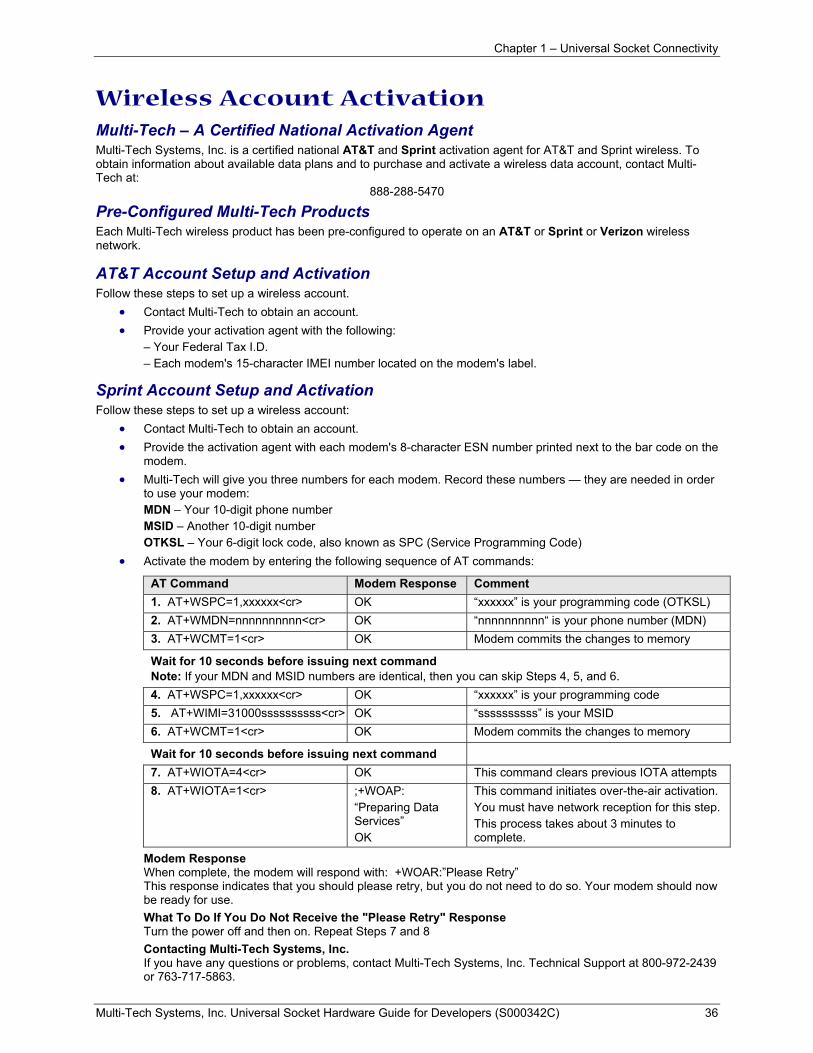
Chapter 1 – Universal Socket Connectivity
Multi-Tech Systems, Inc. Universal Socket Hardware Guide for Developers (S000342C) 36
Wireless Account Activation Multi-Tech – A Certified National Activation Agent Multi-Tech Systems, Inc. is a certified national AT&T and Sprint activation agent for AT&T and Sprint wireless. To obtain information about available data plans and to purchase and activate a wireless data account, contact Multi-Tech at:
888-288-5470
Pre-Configured Multi-Tech Products Each Multi-Tech wireless product has been pre-configured to operate on an AT&T or Sprint or Verizon wireless network.
AT&T Account Setup and Activation Follow these steps to set up a wireless account.
• Contact Multi-Tech to obtain an account. • Provide your activation agent with the following:
– Your Federal Tax I.D. – Each modem's 15-character IMEI number located on the modem's label.
Sprint Account Setup and Activation Follow these steps to set up a wireless account:
• Contact Multi-Tech to obtain an account. • Provide the activation agent with each modem's 8-character ESN number printed next to the bar code on the
modem. • Multi-Tech will give you three numbers for each modem. Record these numbers — they are needed in order
to use your modem: MDN – Your 10-digit phone number MSID – Another 10-digit number OTKSL – Your 6-digit lock code, also known as SPC (Service Programming Code) • Activate the modem by entering the following sequence of AT commands:
AT Command Modem Response Comment 1. AT+WSPC=1,xxxxxx<cr> OK “xxxxxx” is your programming code (OTKSL) 2. AT+WMDN=nnnnnnnnnn<cr> OK “nnnnnnnnnn“ is your phone number (MDN) 3. AT+WCMT=1<cr> OK Modem commits the changes to memory
Wait for 10 seconds before issuing next command Note: If your MDN and MSID numbers are identical, then you can skip Steps 4, 5, and 6. 4. AT+WSPC=1,xxxxxx<cr> OK “xxxxxx” is your programming code 5. AT+WIMI=31000ssssssssss<cr> OK “ssssssssss” is your MSID 6. AT+WCMT=1<cr> OK Modem commits the changes to memory
Wait for 10 seconds before issuing next command
7. AT+WIOTA=4<cr> OK This command clears previous IOTA attempts 8. AT+WIOTA=1<cr> ;+WOAP:
“Preparing Data Services” OK
This command initiates over-the-air activation. You must have network reception for this step. This process takes about 3 minutes to complete.
Modem Response When complete, the modem will respond with: +WOAR:”Please Retry” This response indicates that you should please retry, but you do not need to do so. Your modem should now be ready for use. What To Do If You Do Not Receive the "Please Retry" Response Turn the power off and then on. Repeat Steps 7 and 8 Contacting Multi-Tech Systems, Inc. If you have any questions or problems, contact Multi-Tech Systems, Inc. Technical Support at 800-972-2439 or 763-717-5863.
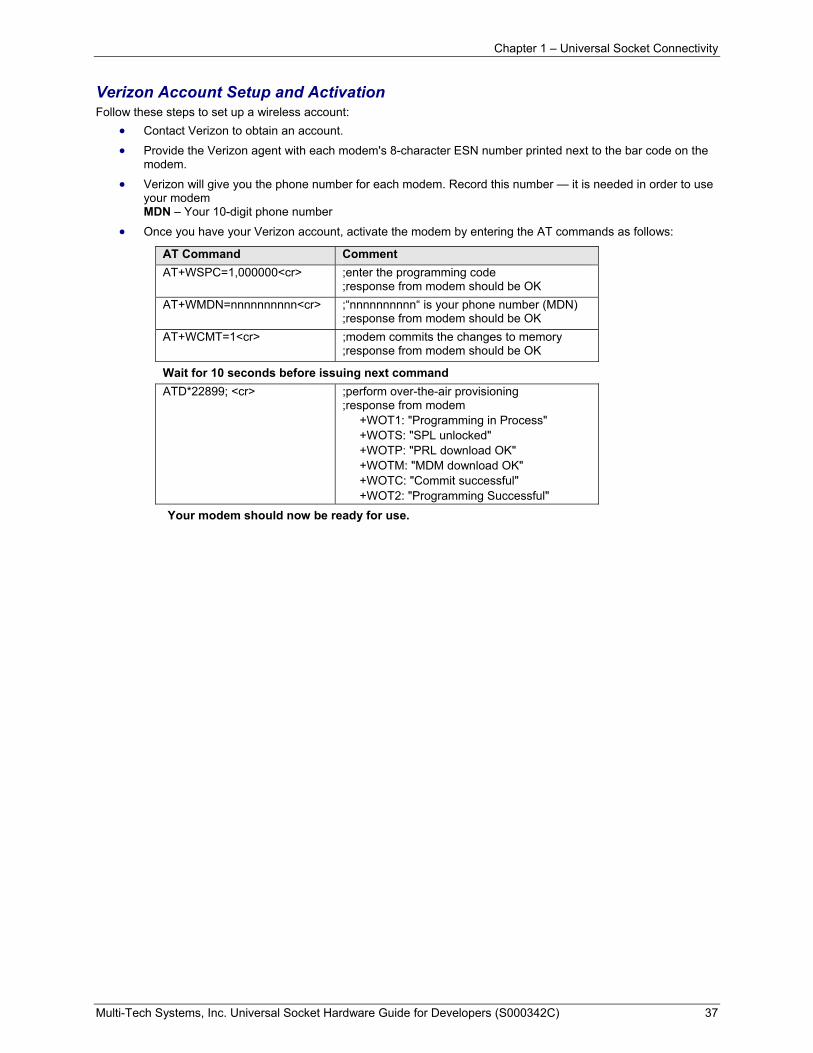
Chapter 1 – Universal Socket Connectivity
Multi-Tech Systems, Inc. Universal Socket Hardware Guide for Developers (S000342C) 37
Verizon Account Setup and Activation Follow these steps to set up a wireless account:
• Contact Verizon to obtain an account. • Provide the Verizon agent with each modem's 8-character ESN number printed next to the bar code on the
modem.
• Verizon will give you the phone number for each modem. Record this number — it is needed in order to use your modem
MDN – Your 10-digit phone number
• Once you have your Verizon account, activate the modem by entering the AT commands as follows:
AT Command Comment AT+WSPC=1,000000<cr> ;enter the programming code
;response from modem should be OK AT+WMDN=nnnnnnnnnn<cr> ;“nnnnnnnnnn“ is your phone number (MDN)
;response from modem should be OK AT+WCMT=1<cr> ;modem commits the changes to memory
;response from modem should be OK
Wait for 10 seconds before issuing next command ATD*22899; <cr> ;perform over-the-air provisioning
;response from modem +WOT1: "Programming in Process" +WOTS: "SPL unlocked" +WOTP: "PRL download OK" +WOTM: "MDM download OK" +WOTC: "Commit successful" +WOT2: "Programming Successful"
Your modem should now be ready for use.

Chapter 1 – Universal Socket Connectivity
Multi-Tech Systems, Inc. Universal Socket Hardware Guide for Developers (S000342C) 38
Multi-Tech Warranty Statement Multi-Tech Systems, Inc., (hereafter “MTS”) warrants that its products will be free from defects in material or workmanship for a period of two, five, or ten years (depending on model) from date of purchase, or if proof of purchase is not provided, two, five, or ten years (depending on model) from date of shipment.
MTS MAKES NO OTHER WARRANTY, EXPRESS OR IMPLIED, AND ALL IMPLIED WARRANTIES OF MERCHANTABILITY AND FITNESS FOR A PARTICULAR PURPOSE ARE HEREBY DISCLAIMED.
This warranty does not apply to any products which have been damaged by lightning storms, water, or power surges or which have been neglected, altered, abused, used for a purpose other than the one for which they were manufactured, repaired by Customer or any party without MTS’s written authorization, or used in any manner inconsistent with MTS’s instructions.
MTS’s entire obligation under this warranty shall be limited (at MTS’s option) to repair or replacement of any products which prove to be defective within the warranty period or, at MTS’s option, issuance of a refund of the purchase price. Defective products must be returned by Customer to MTS’s factory — transportation prepaid.
MTS WILL NOT BE LIABLE FOR CONSEQUENTIAL DAMAGES, AND UNDER NO CIRCUMSTANCES WILL ITS LIABILITY EXCEED THE PRICE FOR DEFECTIVE PRODUCTS.
Repair Procedures for U.S. and Canadian Customers In the event that service is required, products may be shipped, freight prepaid, to our Mounds View, Minnesota factory:
Multi-Tech Systems, Inc. 2205 Woodale Drive Mounds View, MN 55112 Attn: Repairs, Serial # ____________
A Returned Materials Authorization (RMA) is not required. Return shipping charges (surface) will be paid by MTS to destinations in U.S. and Canada.
Please include, inside the shipping box, a description of the problem, a return shipping address (must have street address, not P.O. Box), your telephone number, and if the product is out of warranty, a check or purchase order for repair charges.
For out of warranty repair charges, go to www.multitech.com/DOCUMENTS/Company/warranty/
Extended two-year overnight replacement service agreements are available for selected products. Please call MTS customer service at (888) 288-5470 or visit our web site at www.multitech.com/PARTNERS/Programs/orc/ for details on rates and coverage’s.
Please direct your questions regarding technical matters, product configuration, verification that the product is defective, etc., to our Technical Support department at (800) 972-2439 or email [email protected]. Please direct your questions regarding repair expediting, receiving, shipping, billing, etc., to our Repair Accounting department at (800) 328-9717 or (763) 717-5631, or email [email protected].
Repairs for damages caused by lightning storms, water, power surges, incorrect installation, physical abuse, or user-caused damages are billed on a time-plus-materials basis.
Chapter 1 – Universal Socket Connectivity
Multi-Tech Systems, Inc. Universal Socket Hardware Guide for Developers (S000342C) 39
Repair Procedures for International Customers (Outside U.S.A. and Canada) Your original point of purchase Reseller may offer the quickest and most economical repair option for your Multi-Tech product. You may also contact any Multi-Tech sales office for information about the nearest distributor or other repair service for your Multi-Tech product. The Multi-Tech sales office directory is available at www.multitech.com/PARTNERS/Channels/offices/
In the event that factory service is required, products may be shipped, freight prepaid to our Mounds View, Minnesota factory. Recommended international shipment methods are via Federal Express, UPS or DHL courier services, or by airmail parcel post; shipments made by any other method will be refused. A Returned Materials Authorization (RMA) is required for products shipped from outside the U.S.A. and Canada. Please contact us for return authorization and shipping instructions on any International shipments to the U.S.A. Please include, inside the shipping box, a description of the problem, a return shipping address (must have street address, not P.O. Box), your telephone number, and if the product is out of warranty, a check drawn on a U.S. bank or your company’s purchase order for repair charges. Repaired units shall be shipped freight collect, unless other arrangements are made in advance.
Please direct your questions regarding technical matters, product configuration, verification that the product is defective, etc., to our Technical Support department nearest you or email [email protected]. When calling the U.S., please direct your questions regarding repair expediting, receiving, shipping, billing, etc., to our Repair Accounting department at +(763) 717-5631 in the U.S.A., or email [email protected].
Repairs for damages caused by lightning storms, water, power surges, incorrect installation, physical abuse, or user-caused damages are billed on a time-plus-materials basis.
Repair Procedures for International Distributors International distributors should contact their MTS International sales representative for information about the repairs for their Multi-Tech product.
Please direct your questions regarding technical matters, product configuration, verification that the product is defective, etc., to our International Technical Support department at +(763)717-5863. When calling the U.S., please direct your questions regarding repair expediting, receiving, shipping, billing, etc., to our Repair Accounting department at +(763) 717-5631 in the U.S.A. or email [email protected].
Repairs for damages caused by lightning storms, water, power surges, incorrect installation, physical abuse, or user-caused damages are billed on a time-plus-materials basis.
Replacement Parts SupplyNet, Inc. can supply you with replacement power supplies, cables and connectors for selected Multi-Tech products. You can place an order with SupplyNet via mail, phone, fax or the Internet at the following addresses: Mail: SupplyNet, Inc. 614 Corporate Way Valley Cottage, NY 10989 Phone: 800 826-0279 Fax: 914 267-2420
Email: [email protected]
Internet: http://www.thesupplynet.com
Multi-Tech Systems, Inc. Universal Socket Hardware Guide for Developers (S000342C) 40
Chapter 2
SocketModem
MT5600SMI
MT5656SMI
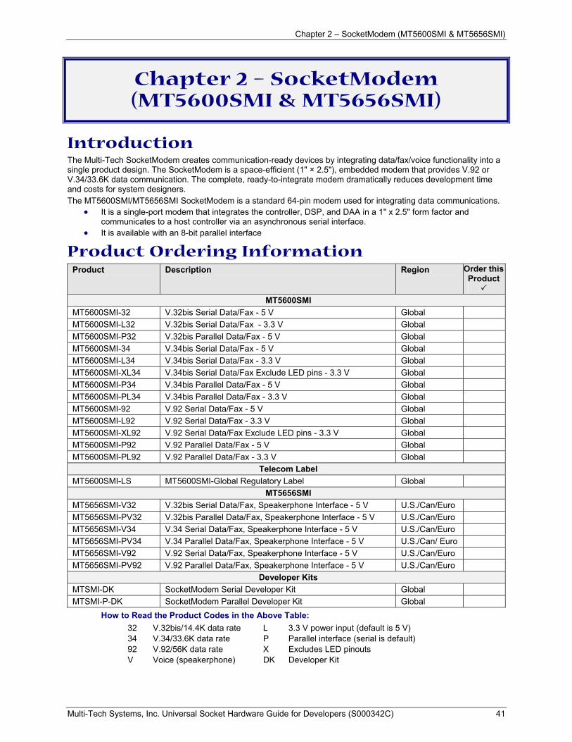
Chapter 2 – SocketModem (MT5600SMI & MT5656SMI)
Multi-Tech Systems, Inc. Universal Socket Hardware Guide for Developers (S000342C) 41
Chapter 2 – SocketModem (MT5600SMI & MT5656SMI)
Introduction The Multi-Tech SocketModem creates communication-ready devices by integrating data/fax/voice functionality into a single product design. The SocketModem is a space-efficient (1" × 2.5"), embedded modem that provides V.92 or V.34/33.6K data communication. The complete, ready-to-integrate modem dramatically reduces development time and costs for system designers. The MT5600SMI/MT5656SMI SocketModem is a standard 64-pin modem used for integrating data communications.
• It is a single-port modem that integrates the controller, DSP, and DAA in a 1" x 2.5" form factor and communicates to a host controller via an asynchronous serial interface.
• It is available with an 8-bit parallel interface
Product Ordering Information Product Description Region Order this
Product
MT5600SMI MT5600SMI-32 V.32bis Serial Data/Fax - 5 V Global MT5600SMI-L32 V.32bis Serial Data/Fax - 3.3 V Global MT5600SMI-P32 V.32bis Parallel Data/Fax - 5 V Global MT5600SMI-34 V.34bis Serial Data/Fax - 5 V Global MT5600SMI-L34 V.34bis Serial Data/Fax - 3.3 V Global MT5600SMI-XL34 V.34bis Serial Data/Fax Exclude LED pins - 3.3 V Global MT5600SMI-P34 V.34bis Parallel Data/Fax - 5 V Global MT5600SMI-PL34 V.34bis Parallel Data/Fax - 3.3 V Global MT5600SMI-92 V.92 Serial Data/Fax - 5 V Global MT5600SMI-L92 V.92 Serial Data/Fax - 3.3 V Global MT5600SMI-XL92 V.92 Serial Data/Fax Exclude LED pins - 3.3 V Global MT5600SMI-P92 V.92 Parallel Data/Fax - 5 V Global MT5600SMI-PL92 V.92 Parallel Data/Fax - 3.3 V Global
Telecom Label MT5600SMI-LS MT5600SMI-Global Regulatory Label Global
MT5656SMI MT5656SMI-V32 V.32bis Serial Data/Fax, Speakerphone Interface - 5 V U.S./Can/Euro MT5656SMI-PV32 V.32bis Parallel Data/Fax, Speakerphone Interface - 5 V U.S./Can/Euro MT5656SMI-V34 V.34 Serial Data/Fax, Speakerphone Interface - 5 V U.S./Can/Euro MT5656SMI-PV34 V.34 Parallel Data/Fax, Speakerphone Interface - 5 V U.S./Can/ Euro MT5656SMI-V92 V.92 Serial Data/Fax, Speakerphone Interface - 5 V U.S./Can/Euro MT5656SMI-PV92 V.92 Parallel Data/Fax, Speakerphone Interface - 5 V U.S./Can/Euro
Developer Kits MTSMI-DK SocketModem Serial Developer Kit Global MTSMI-P-DK SocketModem Parallel Developer Kit Global
How to Read the Product Codes in the Above Table: 32 V.32bis/14.4K data rate L 3.3 V power input (default is 5 V) 34 V.34/33.6K data rate P Parallel interface (serial is default) 92 V.92/56K data rate X Excludes LED pinouts V Voice (speakerphone) DK Developer Kit
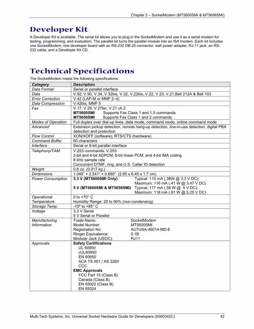
Chapter 2 – SocketModem (MT5600SMI & MT5656SMI)
Multi-Tech Systems, Inc. Universal Socket Hardware Guide for Developers (S000342C) 42
Developer Kit A Developer Kit is available. The serial kit allows you to plug in the SocketModem and use it as a serial modem for testing, programming, and evaluation. The parallel kit turns the parallel module into an ISA modem. Each kit includes one SocketModem, one developer board with an RS-232 DB-25 connector, wall power adapter, RJ-11 jack, an RS-232 cable, and a Developer Kit CD.
Technical Specifications The SocketModem meets the following specifications: Category Description Data Format Serial or parallel interface Data V.92; V.90, V.34, V.32bis, V.32, V.22bis, V.22, V.23, V.21,Bell 212A & Bell 103 Error Correction V.42 (LAP-M or MNP 2–4) Data Compression V.42bis, MNP 5 Fax V.17, V.29, V.27ter, V.21 ch.2
MT5600SMI Supports Fax Class 1 and 1.0 commands MT5656SMI Supports Fax Class 1 and 2 commands
Modes of Operation Full duplex over dial-up lines; data mode, command mode, online command mode Advanced Extension pickup detection, remote hang-up detection, line-in-use detection, digital PBX
detection and protection Flow Control XON/XOFF (software), RTS/CTS (hardware) Command Buffer 60 characters Interface Serial or 8-bit parallel interface Telephony/TAM V.253 commands: V.253
2-bit and 4-bit ADPCM, 8-bit linear PCM, and 4-bit IMA coding 8 kHz sample rate Concurrent DTMF, ring, and U.S. Caller ID detection
Weight 0.6 oz. (0.017 kg.) Dimensions 1.045” × 2.541” × 0.680” (2.65 x 6.45 x 1.7 cm) Power Consumption 3.3 V (MT5600SMI Only) Typical: 115 mA (.38W @ 3.3 V DC);
Maximum: 116 mA (.41 W @ 3.47 V DC) 5 V (MT5600SMI & MT5656SMI) Typical: 117 mA (.58 W @ 5 V DC); Maximum: 118 mA (.61 W @ 5.25 V DC)
Operational Temperature
0 to +70° C Humidity Range: 20 to 90% (non-condensing)
Storage Temp. -10º to +85° C Voltage 3.3 V Serial
5 V Serial or Parallel Manufacturing Information
Trade Name: SocketModem Model Number: MT5600SMI Registration No: AU7USA-46014-MD-E Ringer Equivalence: 0.1B Modular Jack (USOC): RJ11
Approvals Safety Certifications UL 60950 cUL60950 EN 60950 ACA TS 001 / AS 3260 CCC
EMC Approvals FCC Part 15 (Class B) Canada (Class B) EN 55022 (Class B) EN 55024
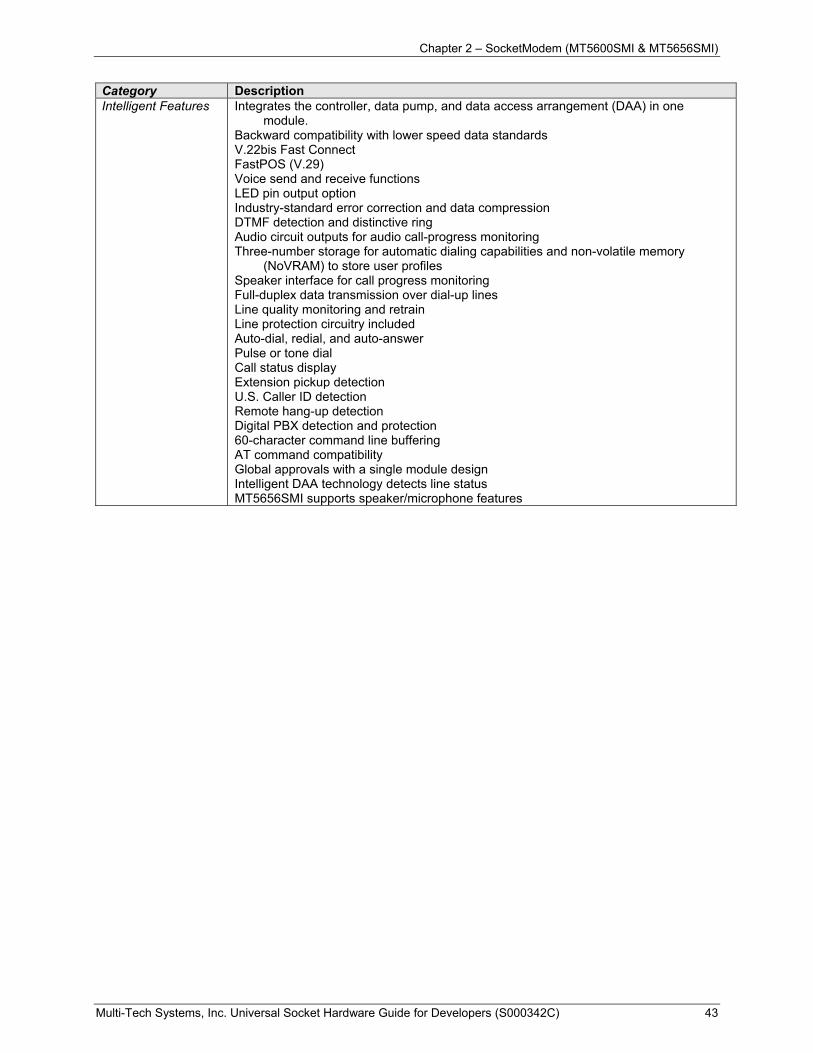
Chapter 2 – SocketModem (MT5600SMI & MT5656SMI)
Multi-Tech Systems, Inc. Universal Socket Hardware Guide for Developers (S000342C) 43
Category Description Intelligent Features
Integrates the controller, data pump, and data access arrangement (DAA) in one module.
Backward compatibility with lower speed data standards V.22bis Fast Connect FastPOS (V.29) Voice send and receive functions LED pin output option Industry-standard error correction and data compression DTMF detection and distinctive ring Audio circuit outputs for audio call-progress monitoring Three-number storage for automatic dialing capabilities and non-volatile memory
(NoVRAM) to store user profiles Speaker interface for call progress monitoring Full-duplex data transmission over dial-up lines Line quality monitoring and retrain Line protection circuitry included Auto-dial, redial, and auto-answer Pulse or tone dial Call status display Extension pickup detection U.S. Caller ID detection Remote hang-up detection Digital PBX detection and protection 60-character command line buffering AT command compatibility Global approvals with a single module design Intelligent DAA technology detects line status MT5656SMI supports speaker/microphone features
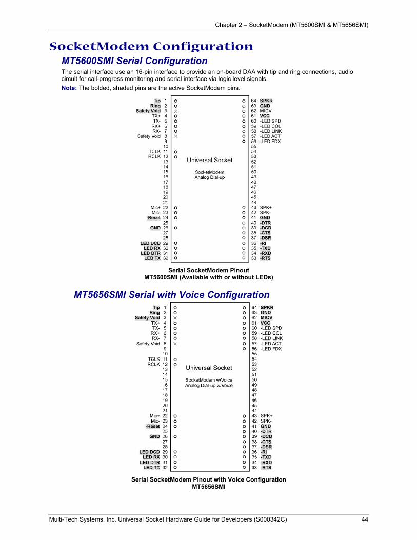
Chapter 2 – SocketModem (MT5600SMI & MT5656SMI)
Multi-Tech Systems, Inc. Universal Socket Hardware Guide for Developers (S000342C) 44
SocketModem Configuration MT5600SMI Serial Configuration The serial interface use an 16-pin interface to provide an on-board DAA with tip and ring connections, audio circuit for call-progress monitoring and serial interface via logic level signals. Note: The bolded, shaded pins are the active SocketModem pins.
Serial SocketModem Pinout
MT5600SMI (Available with or without LEDs)
MT5656SMI Serial with Voice Configuration
Serial SocketModem Pinout with Voice Configuration
MT5656SMI
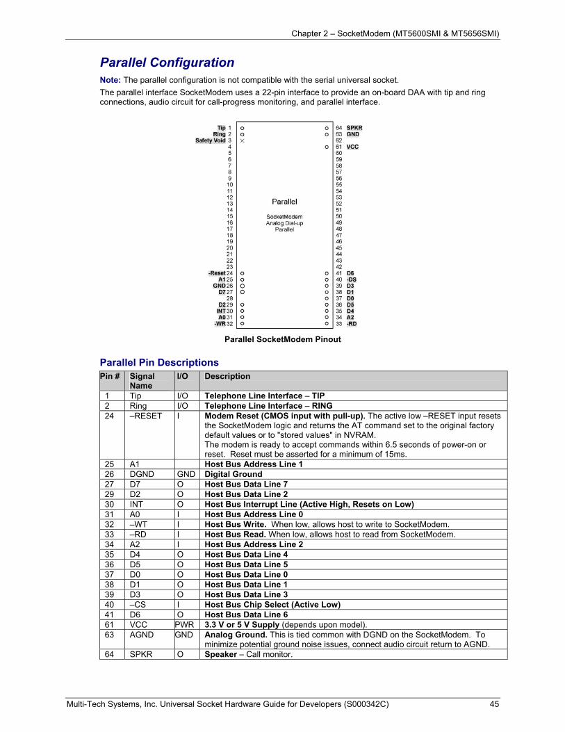
Chapter 2 – SocketModem (MT5600SMI & MT5656SMI)
Multi-Tech Systems, Inc. Universal Socket Hardware Guide for Developers (S000342C) 45
Parallel Configuration Note: The parallel configuration is not compatible with the serial universal socket. The parallel interface SocketModem uses a 22-pin interface to provide an on-board DAA with tip and ring connections, audio circuit for call-progress monitoring, and parallel interface.
Parallel SocketModem Pinout
Parallel Pin Descriptions Pin # Signal
Name I/O Description
1 Tip I/O Telephone Line Interface – TIP 2 Ring I/O Telephone Line Interface – RING 24 –RESET I Modem Reset (CMOS input with pull-up). The active low –RESET input resets
the SocketModem logic and returns the AT command set to the original factory default values or to "stored values" in NVRAM. The modem is ready to accept commands within 6.5 seconds of power-on or reset. Reset must be asserted for a minimum of 15ms.
25 A1 Host Bus Address Line 1 26 DGND GND Digital Ground 27 D7 O Host Bus Data Line 7 29 D2 O Host Bus Data Line 2 30 INT O Host Bus Interrupt Line (Active High, Resets on Low) 31 A0 I Host Bus Address Line 0 32 –WT I Host Bus Write. When low, allows host to write to SocketModem. 33 –RD I Host Bus Read. When low, allows host to read from SocketModem. 34 A2 I Host Bus Address Line 2 35 D4 O Host Bus Data Line 4 36 D5 O Host Bus Data Line 5 37 D0 O Host Bus Data Line 0 38 D1 O Host Bus Data Line 1 39 D3 O Host Bus Data Line 3 40 –CS I Host Bus Chip Select (Active Low) 41 D6 O Host Bus Data Line 6 61 VCC PWR 3.3 V or 5 V Supply (depends upon model). 63 AGND GND Analog Ground. This is tied common with DGND on the SocketModem. To
minimize potential ground noise issues, connect audio circuit return to AGND. 64 SPKR O Speaker – Call monitor.

Chapter 2 – SocketModem (MT5600SMI & MT5656SMI)
Multi-Tech Systems, Inc. Universal Socket Hardware Guide for Developers (S000342C) 46
Differences - Legacy Voice Modems and Current Modems
Differences between the SFxxxD/SP and the MT5656SMI
Note: The SFxxxD/SP is the legacy voice modem with speakerphone I/O. Pin 54 – “VC” This pin provided a reference voltage that is available from the data pump. This pin is not
supported on the MT5656SMI SocketModem. Pin 55 – “~Voice” This function, when active, closes the relay to switch the handset from the telephone line to a
current source to power the handset where it could be used as a speaker and microphone interface to the modem. This pin is not provided on the SocketModem
Pin 57 – “LCS” (Line Current Sense) When enabled, the LCS input indicates whether the associated handset of off-hook (high) or on-hook (low). This pin is not available on the MT5656SMI SocketModem, but the functionality is part of the Smart DAA.
Pin 58 – “Telout” (Telephone Handset Output). This pin is not supported on the SocketModem. Pin 59 – “Telin” (Telephone Handset Input). This pin is not supported on the SocketModem. Pin 60 – “Micm” (Microphone Modem Input). This pin is not supported on the SocketModem. Pin 62 – “Micv” (Microphone Voice Input). This pin is supported on the MT5656SMI SocketModem in the same
way as the "SF" modem.
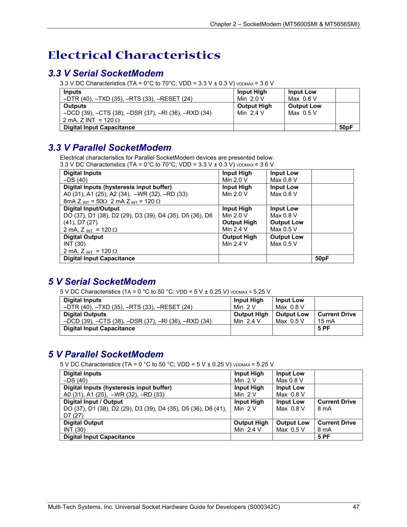
Chapter 2 – SocketModem (MT5600SMI & MT5656SMI)
Multi-Tech Systems, Inc. Universal Socket Hardware Guide for Developers (S000342C) 47
Electrical Characteristics
3.3 V Serial SocketModem 3.3 V DC Characteristics (TA = 0°C to 70°C; VDD = 3.3 V ± 0.3 V) VDDMAX = 3.6 V
Inputs –DTR (40), –TXD (35), –RTS (33), –RESET (24)
Input High Min 2.0 V
Input Low Max 0.8 V
Outputs –DCD (39), –CTS (38), –DSR (37), –RI (36), –RXD (34) 2 mA, Z INT = 120 Ω
Output High Min 2.4 V
Output Low Max 0.5 V
Digital Input Capacitance 50pF
3.3 V Parallel SocketModem Electrical characteristics for Parallel SocketModem devices are presented below. 3.3 V DC Characteristics (TA = 0°C to 70°C; VDD = 3.3 V ± 0.3 V) VDDMAX = 3.6 V
Digital Inputs –DS (40)
Input High Min 2.0 V
Input Low Max 0.8 V
Digital Inputs (hysteresis input buffer) A0 (31), A1 (25), A2 (34), –WR (32), –RD (33) 8mA Z INT = 50Ω 2 mA Z INT = 120 Ω
Input High Min 2.0 V
Input Low Max 0.8 V
Digital Input/Output DO (37), D1 (38), D2 (29), D3 (39), D4 (35), D5 (36), D6 (41), D7 (27) 2 mA, Z INT = 120 Ω
Input High Min 2.0 V Output High Min 2.4 V
Input Low Max 0.8 V Output Low Max 0.5 V
Digital Output INT (30) 2 mA, Z INT = 120 Ω
Output High Min 2.4 V
Output Low Max 0.5 V
Digital Input Capacitance 50pF
5 V Serial SocketModem 5 V DC Characteristics (TA = 0 °C to 50 °C; VDD = 5 V ± 0.25 V) VDDMAX = 5.25 V
Digital Inputs –DTR (40), –TXD (35), –RTS (33), –RESET (24)
Input High Min 2 V
Input Low Max 0.8 V
Digital Outputs –DCD (39), –CTS (38), –DSR (37), –RI (36), –RXD (34)
Output High Min 2.4 V
Output Low Max 0.5 V
Current Drive 15 mA
Digital Input Capacitance 5 PF
5 V Parallel SocketModem 5 V DC Characteristics (TA = 0 °C to 50 °C; VDD = 5 V ± 0.25 V) VDDMAX = 5.25 V
Digital Inputs –DS (40)
Input High Min 2 V
Input Low Max 0.8 V
Digital Inputs (hysteresis input buffer) A0 (31), A1 (25), –WR (32), –RD (33)
Input High Min 2 V
Input Low Max 0.8 V
Digital Input / Output DO (37), D1 (38), D2 (29), D3 (39), D4 (35), D5 (36), D6 (41), D7 (27)
Input High Min 2 V
Input Low Max 0.8 V
Current Drive 8 mA
Digital Output INT (30)
Output High Min 2.4 V
Output Low Max 0.5 V
Current Drive 8 mA
Digital Input Capacitance 5 PF
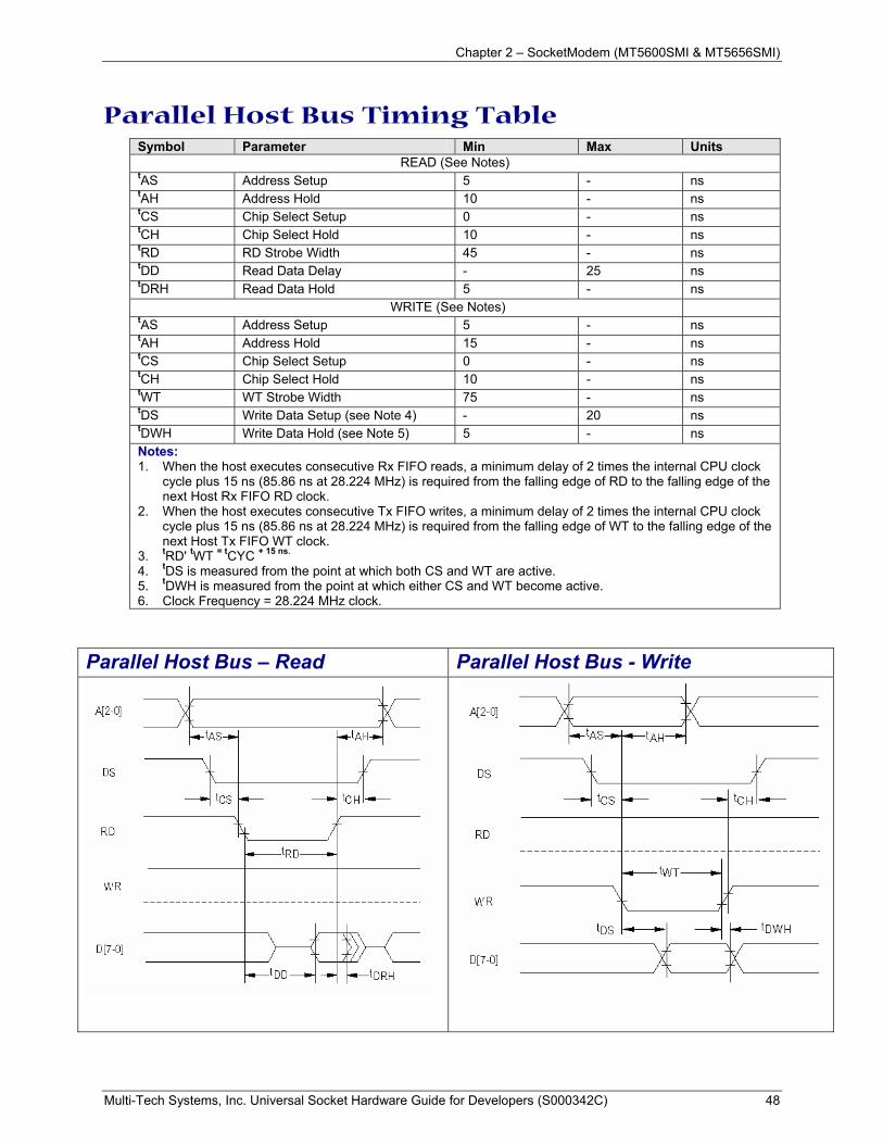
Chapter 2 – SocketModem (MT5600SMI & MT5656SMI)
Multi-Tech Systems, Inc. Universal Socket Hardware Guide for Developers (S000342C) 48
Parallel Host Bus Timing Table Symbol Parameter Min Max Units
READ (See Notes) tAS Address Setup 5 - ns tAH Address Hold 10 - ns tCS Chip Select Setup 0 - ns tCH Chip Select Hold 10 - ns tRD RD Strobe Width 45 - ns tDD Read Data Delay - 25 ns tDRH Read Data Hold 5 - ns
WRITE (See Notes) tAS Address Setup 5 - ns tAH Address Hold 15 - ns tCS Chip Select Setup 0 - ns tCH Chip Select Hold 10 - ns tWT WT Strobe Width 75 - ns tDS Write Data Setup (see Note 4) - 20 ns tDWH Write Data Hold (see Note 5) 5 - ns Notes: 1. When the host executes consecutive Rx FIFO reads, a minimum delay of 2 times the internal CPU clock
cycle plus 15 ns (85.86 ns at 28.224 MHz) is required from the falling edge of RD to the falling edge of the next Host Rx FIFO RD clock.
2. When the host executes consecutive Tx FIFO writes, a minimum delay of 2 times the internal CPU clock cycle plus 15 ns (85.86 ns at 28.224 MHz) is required from the falling edge of WT to the falling edge of the next Host Tx FIFO WT clock.
3. tRD' tWT = tCYC + 15 ns.
4. tDS is measured from the point at which both CS and WT are active. 5. tDWH is measured from the point at which either CS and WT become active. 6. Clock Frequency = 28.224 MHz clock.
Parallel Host Bus – Read Parallel Host Bus - Write
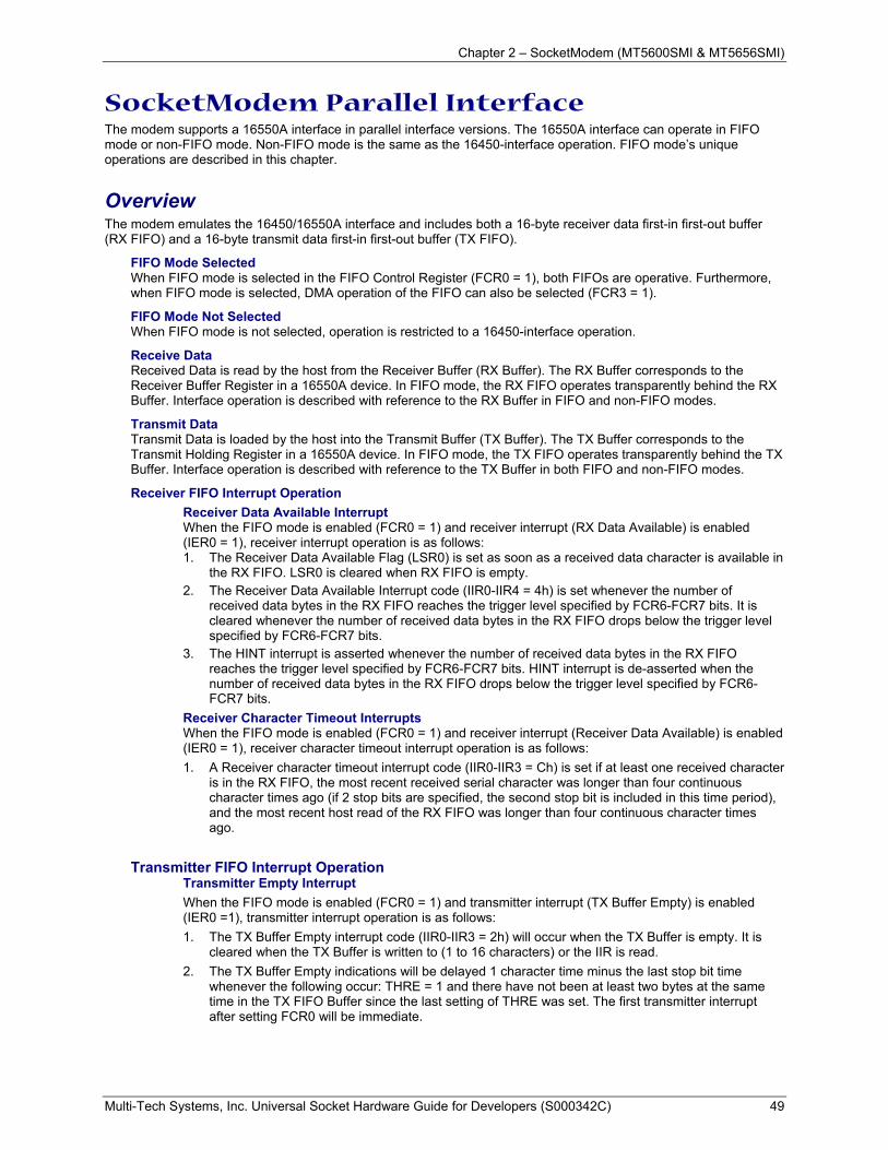
Chapter 2 – SocketModem (MT5600SMI & MT5656SMI)
Multi-Tech Systems, Inc. Universal Socket Hardware Guide for Developers (S000342C) 49
SocketModem Parallel Interface The modem supports a 16550A interface in parallel interface versions. The 16550A interface can operate in FIFO mode or non-FIFO mode. Non-FIFO mode is the same as the 16450-interface operation. FIFO mode’s unique operations are described in this chapter.
Overview The modem emulates the 16450/16550A interface and includes both a 16-byte receiver data first-in first-out buffer (RX FIFO) and a 16-byte transmit data first-in first-out buffer (TX FIFO).
FIFO Mode Selected When FIFO mode is selected in the FIFO Control Register (FCR0 = 1), both FIFOs are operative. Furthermore, when FIFO mode is selected, DMA operation of the FIFO can also be selected (FCR3 = 1).
FIFO Mode Not Selected When FIFO mode is not selected, operation is restricted to a 16450-interface operation.
Receive Data Received Data is read by the host from the Receiver Buffer (RX Buffer). The RX Buffer corresponds to the Receiver Buffer Register in a 16550A device. In FIFO mode, the RX FIFO operates transparently behind the RX Buffer. Interface operation is described with reference to the RX Buffer in FIFO and non-FIFO modes.
Transmit Data Transmit Data is loaded by the host into the Transmit Buffer (TX Buffer). The TX Buffer corresponds to the Transmit Holding Register in a 16550A device. In FIFO mode, the TX FIFO operates transparently behind the TX Buffer. Interface operation is described with reference to the TX Buffer in both FIFO and non-FIFO modes.
Receiver FIFO Interrupt Operation Receiver Data Available Interrupt When the FIFO mode is enabled (FCR0 = 1) and receiver interrupt (RX Data Available) is enabled (IER0 = 1), receiver interrupt operation is as follows: 1. The Receiver Data Available Flag (LSR0) is set as soon as a received data character is available in
the RX FIFO. LSR0 is cleared when RX FIFO is empty. 2. The Receiver Data Available Interrupt code (IIR0-IIR4 = 4h) is set whenever the number of
received data bytes in the RX FIFO reaches the trigger level specified by FCR6-FCR7 bits. It is cleared whenever the number of received data bytes in the RX FIFO drops below the trigger level specified by FCR6-FCR7 bits.
3. The HINT interrupt is asserted whenever the number of received data bytes in the RX FIFO reaches the trigger level specified by FCR6-FCR7 bits. HINT interrupt is de-asserted when the number of received data bytes in the RX FIFO drops below the trigger level specified by FCR6-FCR7 bits.
Receiver Character Timeout Interrupts When the FIFO mode is enabled (FCR0 = 1) and receiver interrupt (Receiver Data Available) is enabled (IER0 = 1), receiver character timeout interrupt operation is as follows: 1. A Receiver character timeout interrupt code (IIR0-IIR3 = Ch) is set if at least one received character
is in the RX FIFO, the most recent received serial character was longer than four continuous character times ago (if 2 stop bits are specified, the second stop bit is included in this time period), and the most recent host read of the RX FIFO was longer than four continuous character times ago.
Transmitter FIFO Interrupt Operation Transmitter Empty Interrupt When the FIFO mode is enabled (FCR0 = 1) and transmitter interrupt (TX Buffer Empty) is enabled (IER0 =1), transmitter interrupt operation is as follows: 1. The TX Buffer Empty interrupt code (IIR0-IIR3 = 2h) will occur when the TX Buffer is empty. It is
cleared when the TX Buffer is written to (1 to 16 characters) or the IIR is read. 2. The TX Buffer Empty indications will be delayed 1 character time minus the last stop bit time
whenever the following occur: THRE = 1 and there have not been at least two bytes at the same time in the TX FIFO Buffer since the last setting of THRE was set. The first transmitter interrupt after setting FCR0 will be immediate.
Chapter 2 – SocketModem (MT5600SMI & MT5656SMI)
Multi-Tech Systems, Inc. Universal Socket Hardware Guide for Developers (S000342C) 50
Register Functional Definitions The following table delineates the assigned bit functions for the twelve internal registers. The assigned bit functions are more fully defined in the following paragraphs.
Internal Registers
BIT No. Register No.
Register Name 7 6 5 4 3 2 1 0
7 Scratch Register (SCR) Scratch Register
6 Modem Status Register (MSR)
Data Carrier Detect (DCD)
Ring Indicator
(RI)
Data Set Ready (DSR)
Clear to Send CTS)
Delta Data Carrier Detect
(DDCD)
Trailing Edge of Ring
Indicator (TERI)
Delta Data Set Ready
(DDSR)
Delta Clear to Send (DCTS)
5 Line Status Register (LSR)
RX FIFO Error
Transmitter Empty
(TEMT)
Transmitter Buffer
Register Empty
(THRE)
Break Interrupt
(BI)
Framing Error (FE)
Parity Error (PE)
Overrun Error (OE)
Receiver Data
Ready (DR)
4 Modem Control Register (MCR)
0 0 0 Local Loopback
Out 2 Out 1 Request to Send (RTS)
Data Terminal Ready (DTR)
3 Line Control Register (LCR)
Divisor Latch
Access Bit (DLAB)
Set Break
Stick Parity
Even Parity Select (EPS)
Parity Enable (PEN)
Number of Stop
Bits (STB)
Word Length Select Bit 1
(WLS1)
Word Length Select Bit 0
(WLSO) 2 Interrupt Identify
Register (IIR) (Read Only)
FIFOs Enabled
FIFOs Enabled
0 0 Pending Interrupt ID
Bit 2
Pending Interrupt ID
Bit 1
Pending Interrupt ID
Bit 0
“0” if Interrupt Pending
2 FIFO Control Register (FCR) (Write Only)
Receiver Trigger MSB
Receiver Trigger
LSB
Reserved Reserved DMA Mode Select
TX FIFO Reset
RX FIFO Reset
FIFO Enable
1 (DLAB = 0)
Interrupt Enable Register (IER)
0 0 0 0 Enable Modem Status
Interrupt (EDSSI)
Enable Receiver
Line Status Interrupt (ELSI)
Enable Transmitter
Holding Register Empty
Interrupt (ETBEI)
Enable Received
Data Available Interrupt (ERBFI)
0 (DLAB = 0)
Transmitter Buffer Register (THR)
Transmitter FIFO Buffer Register (Write Only)
0 (DLAB = 0)
Receiver Buffer Register (RBR)
Receiver FIFO Buffer Register (Read Only)
1 (DLAB = 1)
Divisor Latch MSB Register (DLM)
Divisor Latch MSB
0 (DLAB = 1)
Divisor Latch LSB Register (DLL)
Divisor Latch LSB
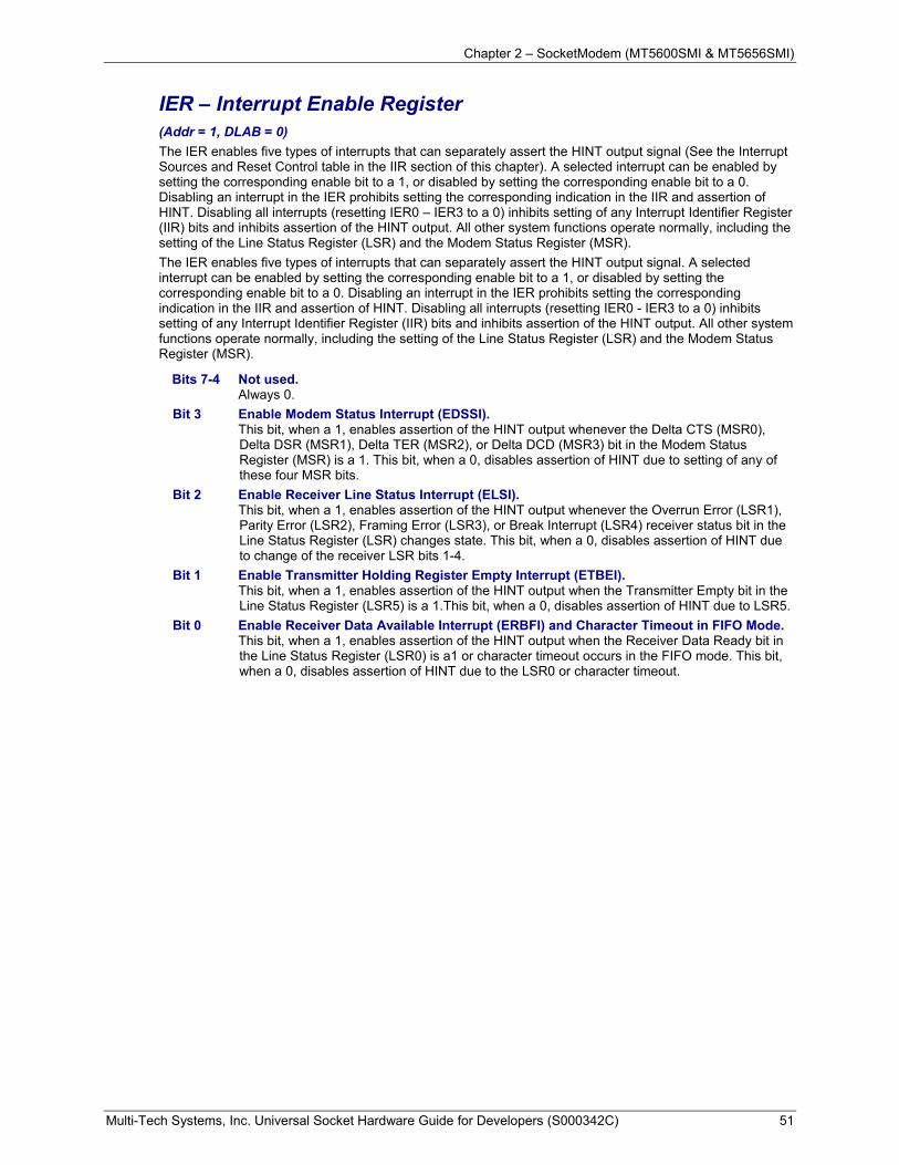
Chapter 2 – SocketModem (MT5600SMI & MT5656SMI)
Multi-Tech Systems, Inc. Universal Socket Hardware Guide for Developers (S000342C) 51
IER – Interrupt Enable Register (Addr = 1, DLAB = 0) The IER enables five types of interrupts that can separately assert the HINT output signal (See the Interrupt Sources and Reset Control table in the IIR section of this chapter). A selected interrupt can be enabled by setting the corresponding enable bit to a 1, or disabled by setting the corresponding enable bit to a 0. Disabling an interrupt in the IER prohibits setting the corresponding indication in the IIR and assertion of HINT. Disabling all interrupts (resetting IER0 – IER3 to a 0) inhibits setting of any Interrupt Identifier Register (IIR) bits and inhibits assertion of the HINT output. All other system functions operate normally, including the setting of the Line Status Register (LSR) and the Modem Status Register (MSR). The IER enables five types of interrupts that can separately assert the HINT output signal. A selected interrupt can be enabled by setting the corresponding enable bit to a 1, or disabled by setting the corresponding enable bit to a 0. Disabling an interrupt in the IER prohibits setting the corresponding indication in the IIR and assertion of HINT. Disabling all interrupts (resetting IER0 - IER3 to a 0) inhibits setting of any Interrupt Identifier Register (IIR) bits and inhibits assertion of the HINT output. All other system functions operate normally, including the setting of the Line Status Register (LSR) and the Modem Status Register (MSR).
Bits 7-4 Not used. Always 0. Bit 3 Enable Modem Status Interrupt (EDSSI). This bit, when a 1, enables assertion of the HINT output whenever the Delta CTS (MSR0),
Delta DSR (MSR1), Delta TER (MSR2), or Delta DCD (MSR3) bit in the Modem Status Register (MSR) is a 1. This bit, when a 0, disables assertion of HINT due to setting of any of these four MSR bits.
Bit 2 Enable Receiver Line Status Interrupt (ELSI). This bit, when a 1, enables assertion of the HINT output whenever the Overrun Error (LSR1),
Parity Error (LSR2), Framing Error (LSR3), or Break Interrupt (LSR4) receiver status bit in the Line Status Register (LSR) changes state. This bit, when a 0, disables assertion of HINT due to change of the receiver LSR bits 1-4.
Bit 1 Enable Transmitter Holding Register Empty Interrupt (ETBEI). This bit, when a 1, enables assertion of the HINT output when the Transmitter Empty bit in the
Line Status Register (LSR5) is a 1.This bit, when a 0, disables assertion of HINT due to LSR5. Bit 0 Enable Receiver Data Available Interrupt (ERBFI) and Character Timeout in FIFO Mode. This bit, when a 1, enables assertion of the HINT output when the Receiver Data Ready bit in
the Line Status Register (LSR0) is a1 or character timeout occurs in the FIFO mode. This bit, when a 0, disables assertion of HINT due to the LSR0 or character timeout.
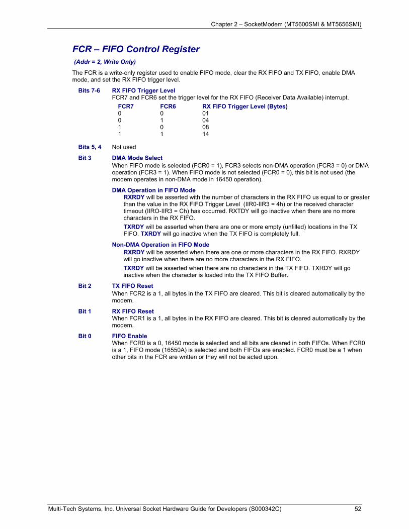
Chapter 2 – SocketModem (MT5600SMI & MT5656SMI)
Multi-Tech Systems, Inc. Universal Socket Hardware Guide for Developers (S000342C) 52
FCR – FIFO Control Register (Addr = 2, Write Only)
The FCR is a write-only register used to enable FIFO mode, clear the RX FIFO and TX FIFO, enable DMA mode, and set the RX FIFO trigger level.
Bits 7-6 RX FIFO Trigger Level FCR7 and FCR6 set the trigger level for the RX FIFO (Receiver Data Available) interrupt.
FCR7 FCR6 RX FIFO Trigger Level (Bytes) 0 0 01 0 1 04 1 0 08 1 1 14
Bits 5, 4 Not used
Bit 3 DMA Mode Select When FIFO mode is selected (FCR0 = 1), FCR3 selects non-DMA operation (FCR3 = 0) or DMA operation (FCR3 = 1). When FIFO mode is not selected (FCR0 = 0), this bit is not used (the modem operates in non-DMA mode in 16450 operation).
DMA Operation in FIFO Mode RXRDY will be asserted with the number of characters in the RX FIFO us equal to or greater than the value in the RX FIFO Trigger Level (IIR0-IIR3 = 4h) or the received character timeout (IIRO-IIR3 = Ch) has occurred. RXTDY will go inactive when there are no more characters in the RX FIFO. TXRDY will be asserted when there are one or more empty (unfilled) locations in the TX FIFO. TXRDY will go inactive when the TX FIFO is completely full.
Non-DMA Operation in FIFO Mode RXRDY will be asserted when there are one or more characters in the RX FIFO. RXRDY will go inactive when there are no more characters in the RX FIFO. TXRDY will be asserted when there are no characters in the TX FIFO. TXRDY will go inactive when the character is loaded into the TX FIFO Buffer.
Bit 2 TX FIFO Reset When FCR2 is a 1, all bytes in the TX FIFO are cleared. This bit is cleared automatically by the modem.
Bit 1 RX FIFO Reset When FCR1 is a 1, all bytes in the RX FIFO are cleared. This bit is cleared automatically by the modem.
Bit 0 FIFO Enable When FCR0 is a 0, 16450 mode is selected and all bits are cleared in both FIFOs. When FCR0 is a 1, FIFO mode (16550A) is selected and both FIFOs are enabled. FCR0 must be a 1 when other bits in the FCR are written or they will not be acted upon.
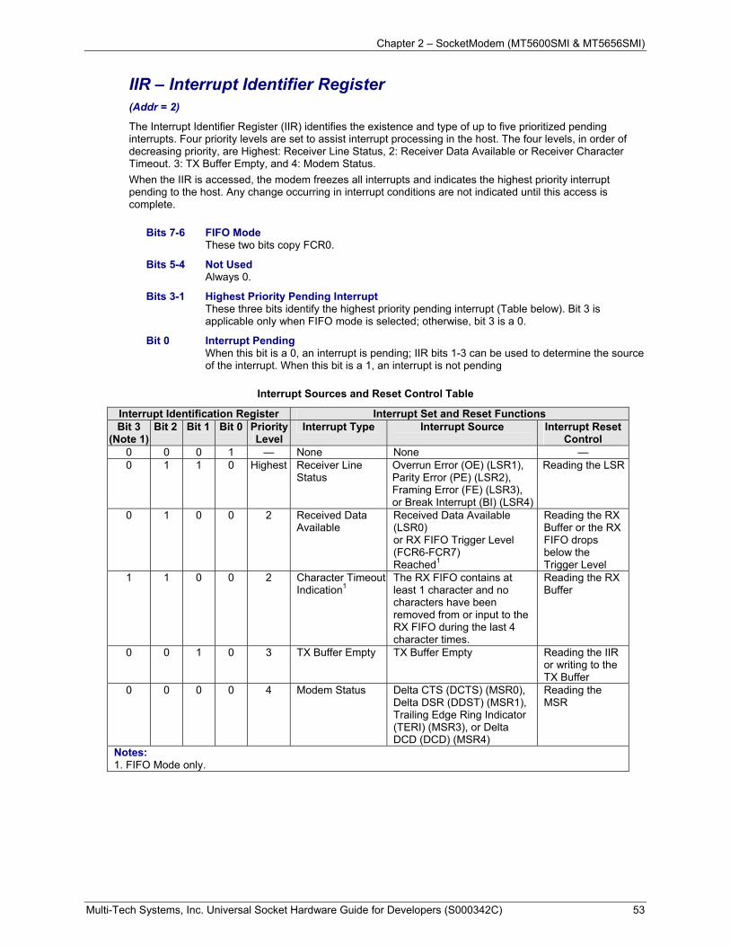
Chapter 2 – SocketModem (MT5600SMI & MT5656SMI)
Multi-Tech Systems, Inc. Universal Socket Hardware Guide for Developers (S000342C) 53
IIR – Interrupt Identifier Register (Addr = 2)
The Interrupt Identifier Register (IIR) identifies the existence and type of up to five prioritized pending interrupts. Four priority levels are set to assist interrupt processing in the host. The four levels, in order of decreasing priority, are Highest: Receiver Line Status, 2: Receiver Data Available or Receiver Character Timeout. 3: TX Buffer Empty, and 4: Modem Status. When the IIR is accessed, the modem freezes all interrupts and indicates the highest priority interrupt pending to the host. Any change occurring in interrupt conditions are not indicated until this access is complete.
Bits 7-6 FIFO Mode
These two bits copy FCR0.
Bits 5-4 Not Used Always 0.
Bits 3-1 Highest Priority Pending Interrupt These three bits identify the highest priority pending interrupt (Table below). Bit 3 is applicable only when FIFO mode is selected; otherwise, bit 3 is a 0.
Bit 0 Interrupt Pending When this bit is a 0, an interrupt is pending; IIR bits 1-3 can be used to determine the source of the interrupt. When this bit is a 1, an interrupt is not pending
Interrupt Sources and Reset Control Table
Interrupt Identification Register Interrupt Set and Reset Functions Bit 3
(Note 1) Bit 2 Bit 1 Bit 0 Priority
Level Interrupt Type Interrupt Source Interrupt Reset
Control 0 0 0 1 — None None — 0 1 1 0 Highest Receiver Line
Status Overrun Error (OE) (LSR1), Parity Error (PE) (LSR2), Framing Error (FE) (LSR3), or Break Interrupt (BI) (LSR4)
Reading the LSR
0 1 0 0 2 Received Data Available
Received Data Available (LSR0) or RX FIFO Trigger Level (FCR6-FCR7) Reached1
Reading the RX Buffer or the RX FIFO drops below the Trigger Level
1 1 0 0 2 Character Timeout Indication1
The RX FIFO contains at least 1 character and no characters have been removed from or input to the RX FIFO during the last 4 character times.
Reading the RX Buffer
0 0 1 0 3 TX Buffer Empty TX Buffer Empty Reading the IIR or writing to the TX Buffer
0 0 0 0 4 Modem Status Delta CTS (DCTS) (MSR0), Delta DSR (DDST) (MSR1), Trailing Edge Ring Indicator (TERI) (MSR3), or Delta DCD (DCD) (MSR4)
Reading the MSR
Notes: 1. FIFO Mode only.
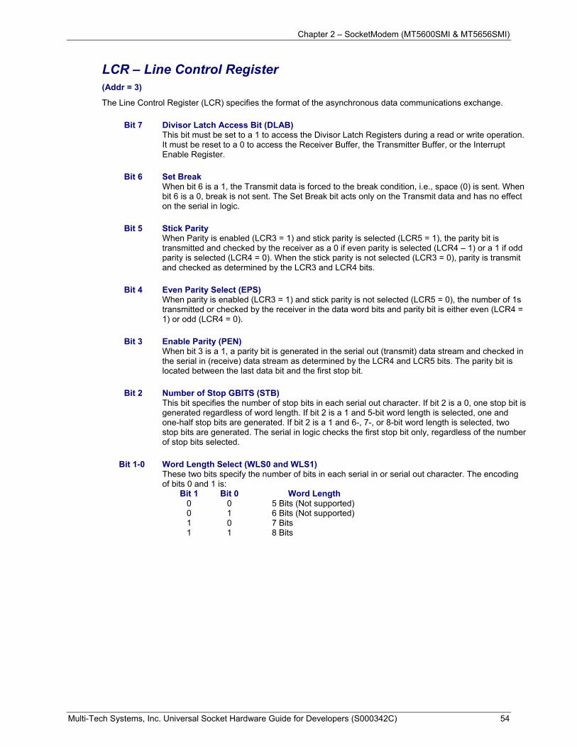
Chapter 2 – SocketModem (MT5600SMI & MT5656SMI)
Multi-Tech Systems, Inc. Universal Socket Hardware Guide for Developers (S000342C) 54
LCR – Line Control Register (Addr = 3)
The Line Control Register (LCR) specifies the format of the asynchronous data communications exchange.
Bit 7 Divisor Latch Access Bit (DLAB) This bit must be set to a 1 to access the Divisor Latch Registers during a read or write operation. It must be reset to a 0 to access the Receiver Buffer, the Transmitter Buffer, or the Interrupt Enable Register.
Bit 6 Set Break When bit 6 is a 1, the Transmit data is forced to the break condition, i.e., space (0) is sent. When bit 6 is a 0, break is not sent. The Set Break bit acts only on the Transmit data and has no effect on the serial in logic.
Bit 5 Stick Parity When Parity is enabled (LCR3 = 1) and stick parity is selected (LCR5 = 1), the parity bit is transmitted and checked by the receiver as a 0 if even parity is selected (LCR4 – 1) or a 1 if odd parity is selected (LCR4 = 0). When the stick parity is not selected (LCR3 = 0), parity is transmit and checked as determined by the LCR3 and LCR4 bits.
Bit 4 Even Parity Select (EPS) When parity is enabled (LCR3 = 1) and stick parity is not selected (LCR5 = 0), the number of 1s transmitted or checked by the receiver in the data word bits and parity bit is either even (LCR4 = 1) or odd (LCR4 = 0).
Bit 3 Enable Parity (PEN) When bit 3 is a 1, a parity bit is generated in the serial out (transmit) data stream and checked in the serial in (receive) data stream as determined by the LCR4 and LCR5 bits. The parity bit is located between the last data bit and the first stop bit.
Bit 2 Number of Stop GBITS (STB) This bit specifies the number of stop bits in each serial out character. If bit 2 is a 0, one stop bit is generated regardless of word length. If bit 2 is a 1 and 5-bit word length is selected, one and one-half stop bits are generated. If bit 2 is a 1 and 6-, 7-, or 8-bit word length is selected, two stop bits are generated. The serial in logic checks the first stop bit only, regardless of the number of stop bits selected.
Bit 1-0 Word Length Select (WLS0 and WLS1) These two bits specify the number of bits in each serial in or serial out character. The encoding of bits 0 and 1 is:
Bit 1 Bit 0 Word Length 0 0 5 Bits (Not supported) 0 1 6 Bits (Not supported) 1 0 7 Bits 1 1 8 Bits
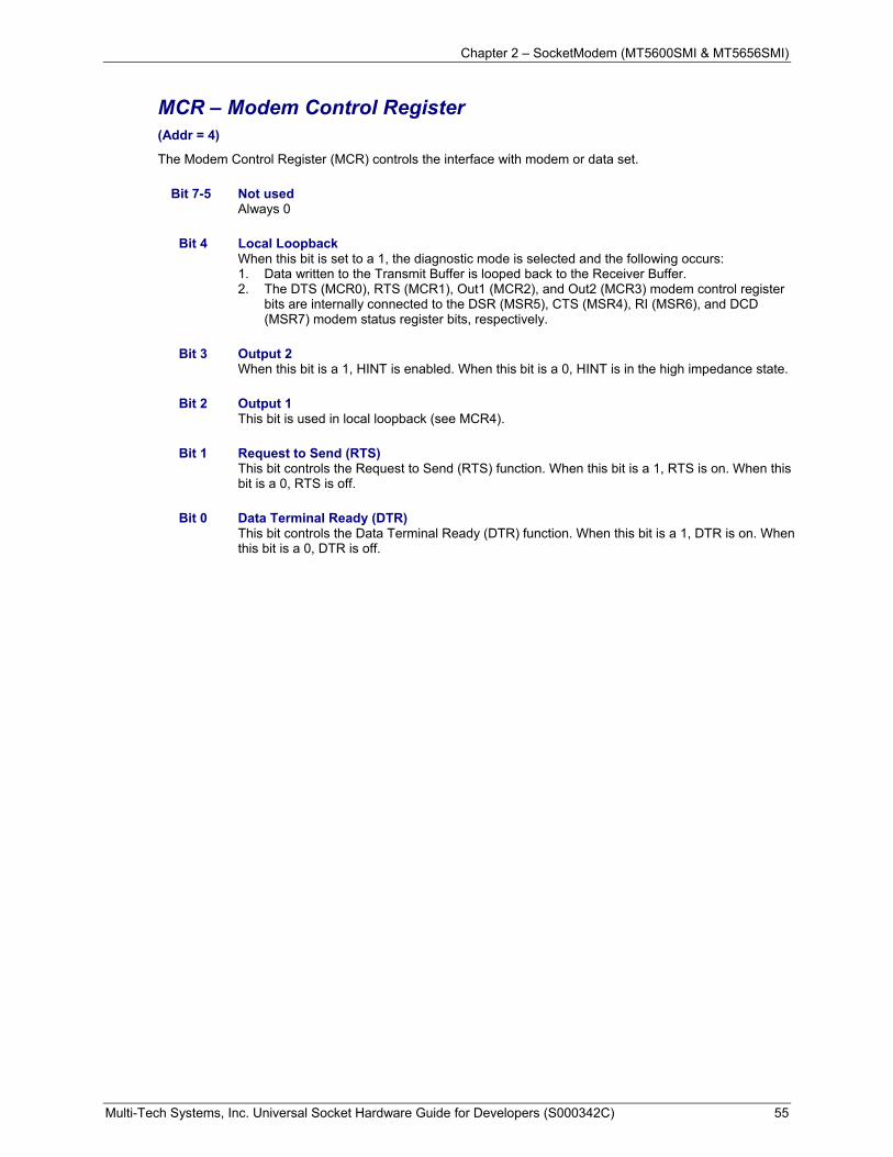
Chapter 2 – SocketModem (MT5600SMI & MT5656SMI)
Multi-Tech Systems, Inc. Universal Socket Hardware Guide for Developers (S000342C) 55
MCR – Modem Control Register (Addr = 4)
The Modem Control Register (MCR) controls the interface with modem or data set.
Bit 7-5 Not used Always 0
Bit 4 Local Loopback When this bit is set to a 1, the diagnostic mode is selected and the following occurs: 1. Data written to the Transmit Buffer is looped back to the Receiver Buffer. 2. The DTS (MCR0), RTS (MCR1), Out1 (MCR2), and Out2 (MCR3) modem control register
bits are internally connected to the DSR (MSR5), CTS (MSR4), RI (MSR6), and DCD (MSR7) modem status register bits, respectively.
Bit 3 Output 2
When this bit is a 1, HINT is enabled. When this bit is a 0, HINT is in the high impedance state.
Bit 2 Output 1 This bit is used in local loopback (see MCR4).
Bit 1 Request to Send (RTS) This bit controls the Request to Send (RTS) function. When this bit is a 1, RTS is on. When this bit is a 0, RTS is off.
Bit 0 Data Terminal Ready (DTR) This bit controls the Data Terminal Ready (DTR) function. When this bit is a 1, DTR is on. When this bit is a 0, DTR is off.
Chapter 2 – SocketModem (MT5600SMI & MT5656SMI)
Multi-Tech Systems, Inc. Universal Socket Hardware Guide for Developers (S000342C) 56
LSR – Line Status Register (Addr = 5)
This 8-bit register provides status information to the host concerning data transfer
Bit 7 RX FIFO Error In the 16450 mode, this bit is not used and is always 0. In the FIFO mode, this bit is set if there are one or more characters in the RX FIFO with parity error, framing error, or break indication detected. This bit is reset to a 0 when the host reads the LSR and note of the above conditions exist in the RX FIFO.
Bit 6 Transmitter Empty (TEMT) This bit is set to a 1 whenever the TX Buffer (THR) and equivalent of the Transmitter Shift Register (TRS) are both empty. It is reset to a 0 whenever either the THR or the equivalent of the TSR contains a character. In the FIFO mode, this bit is set to a 1 whenever the TX FIFO and the equivalent of the TSR are both empty
Bit 5 Transmitter Holding Register Empty (THRE) [TX Buffer Empty] This bit, when set, indicates that the TX Buffer is empty and the modem can accept a new character for transmission. In addition, this bit causes the modem to issue an interrupt to the host when the Transmit Holding Register Empty Interrupt Enable bit (IIR1) is set to 1. The THRE bit is set to a 1 when a character is transferred from the TX Buffer. The bit is reset to 0 when a byte is written into the TX Buffer by the host. In the FIFO mode, this bit is set when the TX FIFO is empty; it is cleared when at lease one byte is in the TX FIFO.
Bit 4 Break Interrupt (BI) This bit is set to a 1 whenever the received data input is a space (logic 0) for longer than two full word lengths plus 3 bits. The BI is reset when the host reads the LSR.
Bit 3 Framing Error (FE) This bit indicates that the received character did not have a valid stop bit. The FE bit is set to a 1 whenever the stop bit following the last data bit or parity bit is detected as a logic o (space). The FE bit is reset to a 0 when the host reads the LSR. In the FIFO mode, the error indication is associated with the particular character in the FIFO it applies to. The FE bit set to a 1 when this character is loaded into the RX Buffer.
Bit 2 Parity Error (PE) This bit indicates that the received data character in the RX Buffer does not have the correct even or odd parity, as selected by the Even Parity Select bit (LCR4) and the Stick Parity bit (LCR5). The PE bit is reset to a 0 when the host reads the LSR. In the FIFO mode, the error indication is associated with the particular character in the FIFO it applies to. The PE bit set to a 1 when this character is loaded into the RX Buffer.
Bit 1 Overrun Error (OE) This bit is set to a 1 whenever received data is loaded into the RX Buffer before the host has read the previous data from the RX Buffer. The OE is reset to a 0 when the host reads the LSR. In the FIFO mode, if data continues to fill beyond the trigger level, an overrun condition will occur only if the RX FIFO is full and the next character has been completely received.
Bit 0 Receiver Data Ready (DR) This bit is set to a 1 whenever a complete incoming character has been received and transferred into the RX Buffer. The DR bit is reset to a 0 when the host reads the RX Buffer. In the FIFO mode, the DR bit is set when the number of received data bytes in the RX FIFO equals or exceeds the trigger level specified in the FCR0-FCR1.
Chapter 2 – SocketModem (MT5600SMI & MT5656SMI)
Multi-Tech Systems, Inc. Universal Socket Hardware Guide for Developers (S000342C) 57
MSR – Modem Status Register (Addr = 6)
The Modem Status Register (MSR) reports current state and change information of the modem. Bits 4-7 supply current state and bits 0-3 supply change information. The change bits are set to a 1 whenever a control input form the modem changes state from the last MSR read by the host. Bits 0-3 are reset to 0 when the host reads the MSR or upon reset. Whenever bits 0, 1, 2, or 3 are set to a 1, a Modem Status Interrupt (IIR0-IIR3 = 0) is generated.
Bit 7 Data Carrier Detect (DCD)
This bit indicates the logic state of the DCH# (RLSD#) output. If Loopback is selected (MCR4 = 1), this bit reflects the state of the Out2 bit in the MCR (MCR3).
Bit 6 Ring Indicator (RI) This bit indicates the logic state of the RI# output. If Loopback is selected (MCR4 = 1), this bit reflects the state of the Out1 bit in the MCR (MCR2).
Bit 5 Data Set Ready (DSR) This bit indicates the logic state of the DSR# output. If Loopback is selected (MCR4 = 1), this bit reflects the state of the DTR in the MCR (MCR0).
Bit 4 Clear to Send (CTS) This bit indicates the logic state of the CTS# output. If Loopback is selected (MCR4 = 1), this bit reflects the state of the RTS bit in the MCR (MCR1).
Bit 3 Delta Data Carrier Detect (DDCD) This bit is set to a 1 when the DCD bit changes state since the host last read the MSR.
Bit 2 Trailing Edge of Ring Indicator (TERI) This bit is set to a 1 when the RI bit changes from a 1 to a 0 state since the host last read the MSR.
Bit 1 Delta Data Set Ready (DDSR) This bit is set to a 1 when the DSR bit has changed since the host last read the MSR.
Bit 0 Delta Clear to Send (DCTS) This bit is set to a 1 when the CTS bit has changed since the MSR the host last read the MSR.
RBX – RX Buffer (Receiver Buffer Register) (Addr = 0, DLAB = 0)
The RX Buffer (RBR) is a read-only register at location 0 (with DLAB = 0). Bit 0 is the least significant bit of the data and is the first bit received.
THR – TX Buffer (Transmitter Holding Register) (Addr = 0, DLAB = 0)
The TX Buffer (THR) is a write-only register at address 0 when DLAB = 0. Bit 0 is the least significant bit and the first bit sent.
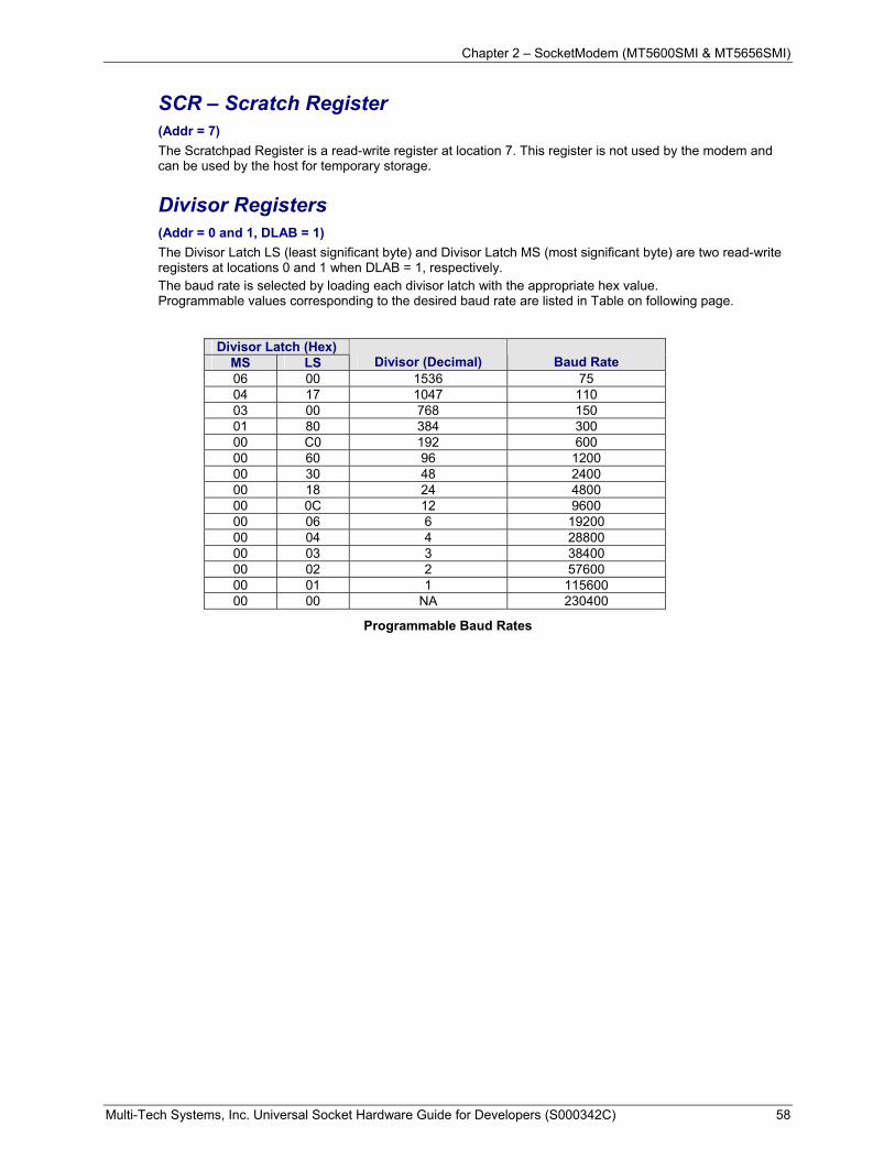
Chapter 2 – SocketModem (MT5600SMI & MT5656SMI)
Multi-Tech Systems, Inc. Universal Socket Hardware Guide for Developers (S000342C) 58
SCR – Scratch Register (Addr = 7) The Scratchpad Register is a read-write register at location 7. This register is not used by the modem and can be used by the host for temporary storage.
Divisor Registers (Addr = 0 and 1, DLAB = 1) The Divisor Latch LS (least significant byte) and Divisor Latch MS (most significant byte) are two read-write registers at locations 0 and 1 when DLAB = 1, respectively. The baud rate is selected by loading each divisor latch with the appropriate hex value. Programmable values corresponding to the desired baud rate are listed in Table on following page.
Divisor Latch (Hex)
MS LS Divisor (Decimal) Baud Rate 06 00 1536 75 04 17 1047 110 03 00 768 150 01 80 384 300 00 C0 192 600 00 60 96 1200 00 30 48 2400 00 18 24 4800 00 0C 12 9600 00 06 6 19200 00 04 4 28800 00 03 3 38400 00 02 2 57600 00 01 1 115600 00 00 NA 230400
Programmable Baud Rates
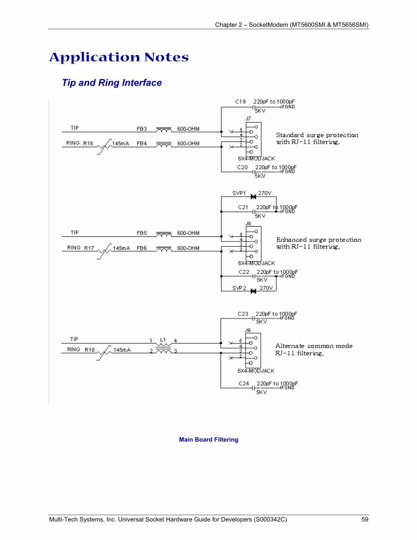
Chapter 2 – SocketModem (MT5600SMI & MT5656SMI)
Multi-Tech Systems, Inc. Universal Socket Hardware Guide for Developers (S000342C) 59
Application Notes
Tip and Ring Interface
Main Board Filtering
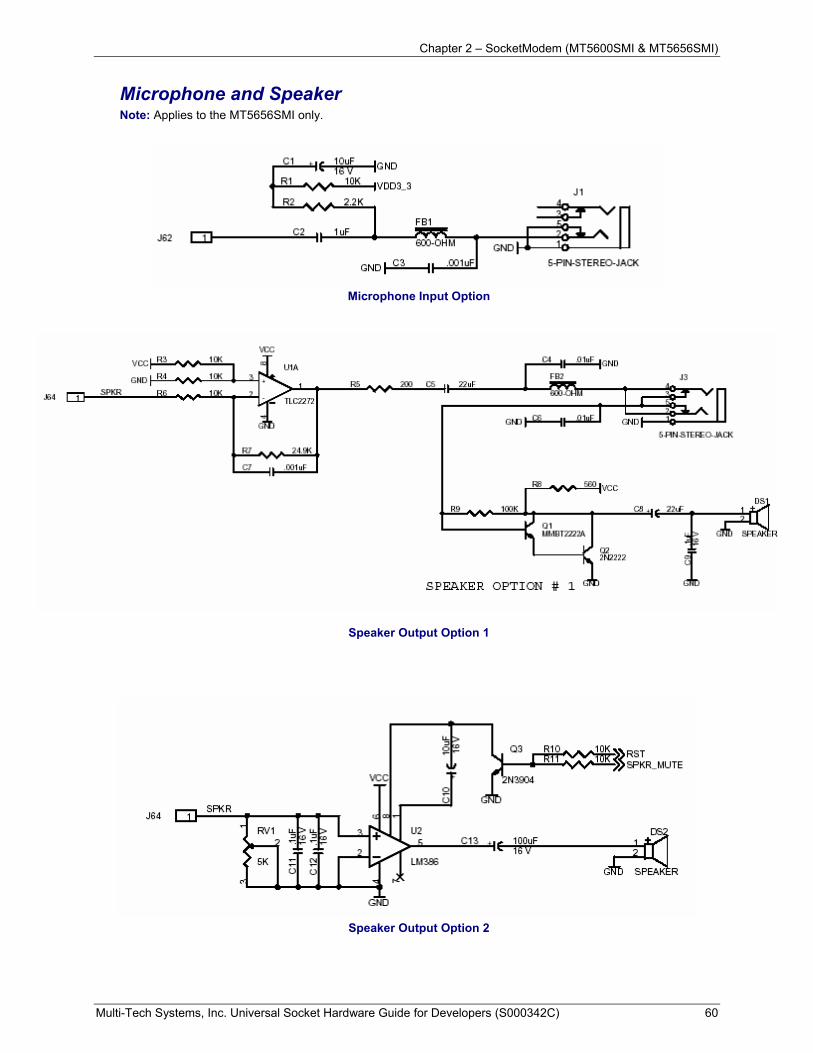
Chapter 2 – SocketModem (MT5600SMI & MT5656SMI)
Multi-Tech Systems, Inc. Universal Socket Hardware Guide for Developers (S000342C) 60
Microphone and Speaker Note: Applies to the MT5656SMI only.
Microphone Input Option
Speaker Output Option 1
Speaker Output Option 2
Chapter 2 – SocketModem (MT5600SMI & MT5656SMI)
Multi-Tech Systems, Inc. Universal Socket Hardware Guide for Developers (S000342C) 61
Recommended Parts
Disclaimer: Multi-Tech Systems makes no warranty claims for vendor product recommendations listed below. Other vendor products may or may not operate satisfactorily. Multi-Tech System’s recommended vendor products only indicate that the product has been tested in controlled conditions and were found to perform satisfactorily.
Surface mount ferrites are used on T&R (Tip and Ring) to mitigate emission levels out the RJ-11 cable. 220pF capacitors are also used on T&R to reduce the common mode emissions that may be present in certain systems. The ferrite and capacitors also aid in reducing the effects of transients that may be present on the line.
Recommended Ferrite (SMT) Manufacturer – Associated Component Technology (ACT) – Part # - YCB-1206 Manufacturer – Murata Erie – Part # - BLM31AJ601SN1
Recommended Ferrite (Thru-Hole) Manufacturer – Associated Component Technology (ACT) – Part # - WB2-2.OT
Recommended Capacitor Manufacturer – NOVACAP – Part # - ES2211NKES502NXT Manufacturer – Murata Erie – Part # - GA355DR7GC221KY02L (Surface mount device)
Part # - DE0807B221K-KH (Thru-hole device) Manufacturer – Ever Grace Electronic Industrials -- Part # - YP221K2EA7PS Note: The capacitors used on T&R must have the Y2 safety rating.
Recommended Connector Manufacturer – Stewart – Part # - SS-6446-NF-A431
Recommended Poly Switch Thermal Fuse (can be reset) Manufacturer – RayChem – Part # - TS600-170 Note: This fuse or its equivalent is required to meet UL60950 for protection against over-voltage from power line crosses.
Telecom The RJ-11 connector must meet FCC Part 68 requirements. Refer to FCC Part 68 section 68.500 subpart F for connector specifications. A self-healing fuse is used in series with line to help prevent damage to the DAA circuit. This fuse is needed for FCC Part 68 compliance.
Common Mode Choke Manufacturer – TDK – Part # - ZJYS51R5-2PT
Recommended Sidactor Manufacturer – Teccor Electronics – Part # - P#3100SA Manufacturer – ST Microelectronics -- Part 1 – SMP100LC-270
Recommended Transceiver Manufacturer – Analog Devices – Part # - ADM207EAR
Multi-Tech Systems, Inc. Universal Socket Hardware Guide for Developers (S000342C) 62
Chapter 3
SocketModem
MT5634SMI-34 MT5634SMI-92
Chapter 3 – SocketModem (MT5634SMI-34 & MT5634SMI-92)
Multi-Tech Systems, Inc. Universal Socket Hardware Guide for Developers (S000342C) 63
Chapter 3 – SocketModem (MT5634SMI-34 & MT5634SMI-92)
Introduction Multi-Tech’s SocketModem creates communication-ready devices by integrating data/fax/voice functionality into a single product design. The SocketModem is a space-efficient (1" × 2.5"), embedded modem that provides V.92/56K communication. The complete, ready-to-integrate modem dramatically reduces development time and costs for system designers.
The MT5634SMI SocketModem is used for integrating data and fax communications:
• It is a single-port modem, which integrates the controller, DSP, and DAA in a 1" x 2.5" form factor and communicates to a host controller via an asynchronous serial interface
• It is available with an 8-bit parallel interface
Product Ordering Information Product Description Region
Order this
Product
MT5634SMI-34 V.34 Serial Data V.34 Fax - 5 V Global MT5634SMI-92 V.92 Serial Data V.34 Fax - 5 V Global MT5634SMI-P-92 V.92 Parallel Data V.34 Fax - 5 V Global MT5634SMI-ITP-92 V.92 Serial Data V.34 Fax - Industrial Temperature - 3.3 V Global MT5634SMI-P-ITP-92 V.92 Parallel Data V.34 Fax - Industrial Temperature - 3.3 V Global MT5634SMI-HV-92 V.92 Serial Data V.34 Fax - High Voltage Medical Device - 5 V Global MT5634SMI-P-HV-92 V.92 Parallel Data V.34 Fax - High Voltage Medical Device - 5 V Global
Telecom Label MT5634SMI-LS MT5634SMI – Global Regulatory Label Global
Developer Kits MTSMI-DK SocketModem Serial Developer Kit Global MTSMI-P-DK SocketModem Parallel Developer Kit Global
How to Read the Product Codes in the Table Above: 34 V.34/33.6K data rate 92 V.92/56K data rate HV High Voltage Medical Device Build ITP Industrial Temperature Build P Parallel interface (serial is default) LS Telecom Label DK Developer Kit
Developer Kit Two SocketModem Developer Kits are available, one for serial and the other for parallel. The serial kit allows you to plug in the SocketModem and use it as a serial modem for testing, programming, and evaluation. The parallel kit turns the parallel module into an ISA modem. Each kit includes one developer board with an RS-232 DB-25 connector, wall power adapter, RJ-11 jack, an RS-232 cable, and a Developer Kit CD.
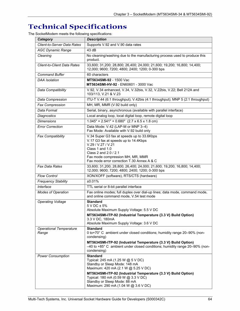
Chapter 3 – SocketModem (MT5634SMI-34 & MT5634SMI-92)
Multi-Tech Systems, Inc. Universal Socket Hardware Guide for Developers (S000342C) 64
Technical Specifications The SocketModem meets the following specifications:
Category Description Client-to-Server Data Rates Supports V.92 and V.90 data rates AGC Dynamic Range 43 dB Cleaning No cleaning/washing due to the manufacturing process used to produce this
product. Client-to-Client Data Rates 33,600; 31,200; 28,800; 26,400; 24,000; 21,600; 19,200; 16,800; 14,400;
12,000; 9600; 7200; 4800; 2400; 1200; 0-300 bps Command Buffer 60 characters DAA Isolation
MT5634SMI-92 - 1500 Vac MT5634SMI-HV-92 - EN60601 - 3000 Vac
Data Compatibility V.92, V.34 enhanced, V.34, V.32bis, V.32, V.22bis, V.22; Bell 212A and 103/113, V.21 & V.23
Data Compression ITU-T V.44 (6:1 throughput); V.42bis (4:1 throughput); MNP 5 (2:1 throughput) Fax Compression MH, MR, MMR (V.92 build only) Data Format Serial, binary, asynchronous (available with parallel interface) Diagnostics Local analog loop, local digital loop, remote digital loop Dimensions 1.045" × 2.541" × 0.680" (2.7 x 6.5 x 1.8 cm) Error Correction Data Mode: V.42 (LAP-M or MNP 3–4)
Fax Mode: Available with V.92 build only Fax Compatibility V.34 Super G3 fax at speeds up to 33.6Kbps
V.17 G3 fax at speeds up to 14.4Kbps V.29 / V.27 / V.21 Class 1 and 1.0 Class 2 and 2.0 / 2.1 Fax mode compression MH, MR, MMR Fax mode error correction T.30 Annex A & C
Fax Data Rates 33,600; 31,200; 28,800; 26,400; 24,000; 21,600; 19,200; 16,800; 14,400; 12,000; 9600; 7200; 4800; 2400; 1200; 0-300 bps
Flow Control XON/XOFF (software), RTS/CTS (hardware) Frequency Stability ±0.01% Interface TTL serial or 8-bit parallel interface Modes of Operation Fax online modes; full duplex over dial-up lines; data mode, command mode,
and online command mode, V.54 test mode Operating Voltage Standard
5 V DC ± 5% Absolute Maximum Supply Voltage: 5.5 V DC MT5634SMI-ITP-92 (Industrial Temperature 3.3 V Build Option) 3.3 V DC, 180mA Absolute Maximum Supply Voltage: 3.6 V DC
Operational Temperature Range
Standard 0 to+70° C ambient under closed conditions; humidity range 20–90% (non-condensing) MT5634SMI-ITP-92 (Industrial Temperature 3.3 V Build Option) –40 to +85° C ambient under closed conditions; humidity range 20–90% (non-condensing)
Power Consumption Standard Typical: 245 mA (1.25 W @ 5 V DC) Standby or Sleep Mode: 148 mA Maximum: 420 mA (2.1 W @ 5.25 V DC) MT5634SMI-ITP-92 (Industrial Temperature 3.3 V Build Option) Typical: 180 mA (0.59 W @ 3.3 V DC) Standby or Sleep Mode: 88 mA Maximum: 290 mA (1.04 W @ 3.6 V DC)
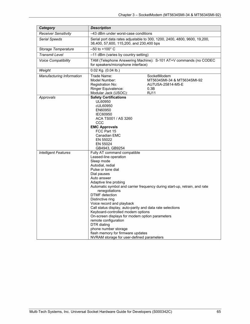
Chapter 3 – SocketModem (MT5634SMI-34 & MT5634SMI-92)
Multi-Tech Systems, Inc. Universal Socket Hardware Guide for Developers (S000342C) 65
Category Description Receiver Sensitivity –43 dBm under worst-case conditions Serial Speeds Serial port data rates adjustable to 300, 1200, 2400, 4800, 9600, 19,200,
38,400, 57,600, 115,200, and 230,400 bps Storage Temperature –50 to +100° C Transmit Level –11 dBm (varies by country setting) Voice Compatibility TAM (Telephone Answering Machine): S-101 AT+V commands (no CODEC
for speakers/microphone interface) Weight 0.02 Kg. (0.04 lb.) Manufacturing Information Trade Name: SocketModem
Model Number: MT5634SMI-34 & MT5634SMI-92 Registration No: AU7USA-25814-M5-E Ringer Equivalence: 0.3B Modular Jack (USOC): RJ11
Approvals Safety Certifications UL60950 cUL60950 EN60950 IEC60950 ACA TS001 / AS 3260 CCC
EMC Approvals FCC Part 15 Canadian EMC EN 55022 EN 55024 GB4943, GB9254
Intelligent Features Fully AT command compatible Leased-line operation Sleep mode Autodial, redial Pulse or tone dial Dial pauses Auto answer Adaptive line probing Automatic symbol and carrier frequency during start-up, retrain, and rate
renegotiations DTMF detection Distinctive ring Voice record and playback Call status display, auto-parity and data rate selections Keyboard-controlled modem options On-screen displays for modem option parameters remote configuration DTR dialing phone number storage flash memory for firmware updates NVRAM storage for user-defined parameters
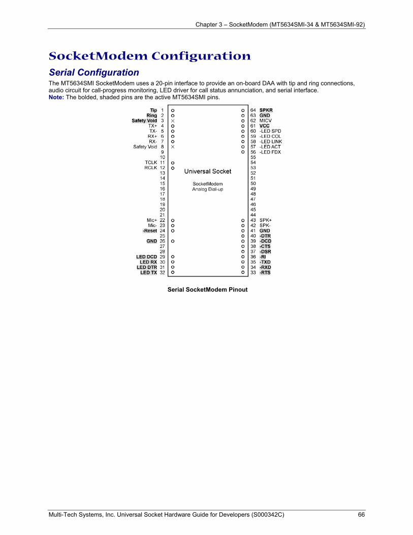
Chapter 3 – SocketModem (MT5634SMI-34 & MT5634SMI-92)
Multi-Tech Systems, Inc. Universal Socket Hardware Guide for Developers (S000342C) 66
SocketModem Configuration
Serial Configuration The MT5634SMI SocketModem uses a 20-pin interface to provide an on-board DAA with tip and ring connections, audio circuit for call-progress monitoring, LED driver for call status annunciation, and serial interface. Note: The bolded, shaded pins are the active MT5634SMI pins.
Serial SocketModem Pinout
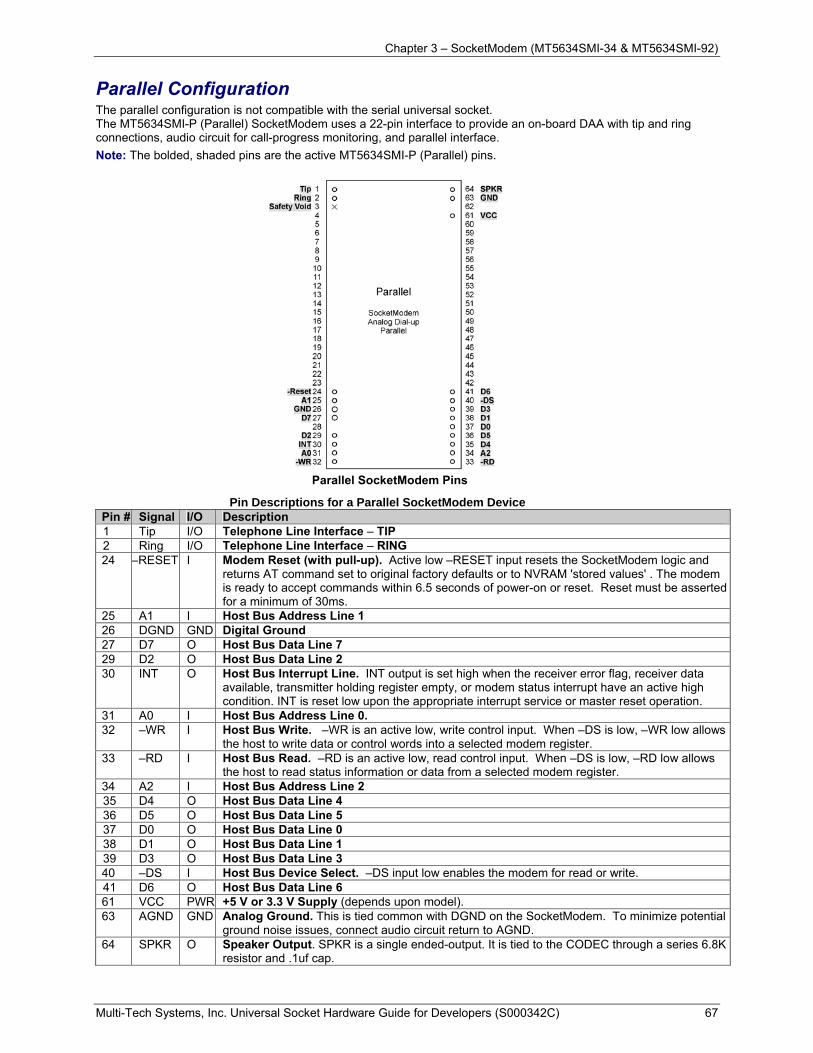
Chapter 3 – SocketModem (MT5634SMI-34 & MT5634SMI-92)
Multi-Tech Systems, Inc. Universal Socket Hardware Guide for Developers (S000342C) 67
Parallel Configuration The parallel configuration is not compatible with the serial universal socket. The MT5634SMI-P (Parallel) SocketModem uses a 22-pin interface to provide an on-board DAA with tip and ring connections, audio circuit for call-progress monitoring, and parallel interface. Note: The bolded, shaded pins are the active MT5634SMI-P (Parallel) pins.
Parallel SocketModem Pins
Pin Descriptions for a Parallel SocketModem Device Pin # Signal I/O Description 1 Tip I/O Telephone Line Interface – TIP 2 Ring I/O Telephone Line Interface – RING 24 –RESET I Modem Reset (with pull-up). Active low –RESET input resets the SocketModem logic and
returns AT command set to original factory defaults or to NVRAM 'stored values' . The modem is ready to accept commands within 6.5 seconds of power-on or reset. Reset must be asserted for a minimum of 30ms.
25 A1 I Host Bus Address Line 1 26 DGND GND Digital Ground 27 D7 O Host Bus Data Line 7 29 D2 O Host Bus Data Line 2 30 INT O Host Bus Interrupt Line. INT output is set high when the receiver error flag, receiver data
available, transmitter holding register empty, or modem status interrupt have an active high condition. INT is reset low upon the appropriate interrupt service or master reset operation.
31 A0 I Host Bus Address Line 0. 32 –WR I Host Bus Write. –WR is an active low, write control input. When –DS is low, –WR low allows
the host to write data or control words into a selected modem register. 33 –RD I Host Bus Read. –RD is an active low, read control input. When –DS is low, –RD low allows
the host to read status information or data from a selected modem register. 34 A2 I Host Bus Address Line 2 35 D4 O Host Bus Data Line 4 36 D5 O Host Bus Data Line 5 37 D0 O Host Bus Data Line 0 38 D1 O Host Bus Data Line 1 39 D3 O Host Bus Data Line 3 40 –DS I Host Bus Device Select. –DS input low enables the modem for read or write. 41 D6 O Host Bus Data Line 6 61 VCC PWR +5 V or 3.3 V Supply (depends upon model). 63 AGND GND Analog Ground. This is tied common with DGND on the SocketModem. To minimize potential
ground noise issues, connect audio circuit return to AGND. 64 SPKR O Speaker Output. SPKR is a single ended-output. It is tied to the CODEC through a series 6.8K
resistor and .1uf cap.
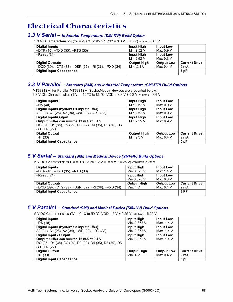
Chapter 3 – SocketModem (MT5634SMI-34 & MT5634SMI-92)
Multi-Tech Systems, Inc. Universal Socket Hardware Guide for Developers (S000342C) 68
Electrical Characteristics
3.3 V Serial – Industrial Temperature (SMI-ITP) Build Option 3.3 V DC Characteristics (TA = -40 °C to 85 °C; VDD = 3.3 V ± 0.3 V) VDDMAX = 3.6 V
Digital Inputs –DTR (40), –TXD (35), –RTS (33)
Input High Min 2.52 V
Input Low Max 0.9 V
–Reset (24) Input High Min 2.52 V
Input Low Max 0.3 V
Digital Outputs –DCD (39), –CTS (38), –DSR (37), –RI (36), –RXD (34)
Output High Min. 2.3 V
Output Low Max 0.4 V
Current Drive 2 mA
Digital Input Capacitance 5 pF
3.3 V Parallel – Standard (SMI) and Industrial Temperature (SMI-ITP) Build Options MT5634SMI for Parallel MT5634SMI SocketModem devices are presented below. 3.3 V DC Characteristics (TA = –40 °C to 85 °C; VDD = 3.3 V ± 0.3 V) VDDMAX = 3.6 V
Digital Inputs –DS (40)
Input High Min 2.52 V
Input Low Max 0.9 V
Digital Inputs (hysteresis input buffer) A0 (31), A1 (25), A2 (34), –WR (32), –RD (33)
Input High Min 2.52 V
Input Low Max 0.9 V
Digital Input/Output Output buffer can source 12 mA at 0.4 V DO (37), D1 (38), D2 (29), D3 (39), D4 (35), D5 (36), D6 (41), D7 (27)
Input High Min 2.52 V
Input Low Max 0.9 V
Digital Output INT (30)
Output High Min 2.3 V
Output Low Max 0.4 V
Current Drive 2 mA
Digital Input Capacitance 5 pF
5 V Serial – Standard (SMI) and Medical Device (SMI-HV) Build Options 5 V DC Characteristics (TA = 0 °C to 50 °C; VDD = 5 V ± 0.25 V) VDDMAX = 5.25 V
Digital Inputs –DTR (40), –TXD (35), –RTS (33)
Input High Min 3.675 V
Input Low Max 1.4 V
–Reset (24) Input High Min 3.675 V
Input Low Max 0.3 V
Digital Outputs –DCD (39), –CTS (38), –DSR (37), –RI (36), –RXD (34)
Output High Min. 4 V
Output Low Max 0.4 V
Current Drive 2 mA
Digital Input Capacitance 5 PF
5 V Parallel – Standard (SMI) and Medical Device (SMI-HV) Build Options 5 V DC Characteristics (TA = 0 °C to 50 °C; VDD = 5 V ± 0.25 V) VDDMAX = 5.25 V
Digital Inputs –DS (40)
Input High Min. 3.675 V
Input Low Max. 1.4 V
Digital Inputs (hysteresis input buffer) A0 (31), A1 (25), A2 (34), –WR (32), –RD (33)
Input High Min. 3.675 V
Input Low Max. 1.4 V
Digital Input / Output Output buffer can source 12 mA at 0.4 V DO (37), D1 (38), D2 (29), D3 (39), D4 (35), D5 (36), D6 (41), D7 (27)
Input High Min. 3.675 V
Input Low Max. 1.4 V
Digital Output INT (30)
Output High Min. 4 V
Output Low Max 0.4 V
Current Drive 2 mA
Digital Input Capacitance 5 pF
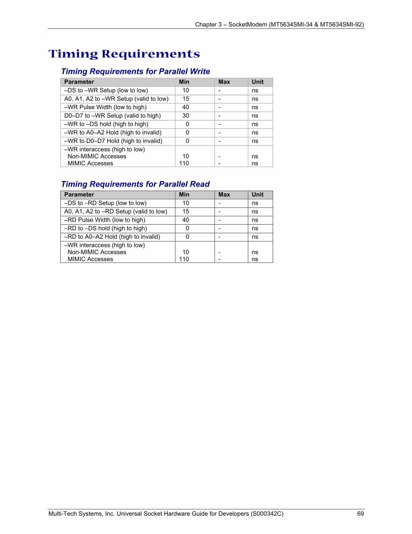
Chapter 3 – SocketModem (MT5634SMI-34 & MT5634SMI-92)
Multi-Tech Systems, Inc. Universal Socket Hardware Guide for Developers (S000342C) 69
Timing Requirements
Timing Requirements for Parallel Write Parameter Min Max Unit –DS to –WR Setup (low to low) 10 - ns A0, A1, A2 to –WR Setup (valid to low) 15 - ns –WR Pulse Width (low to high) 40 - ns D0–D7 to –WR Setup (valid to high) 30 - ns –WR to –DS hold (high to high) 0 - ns –WR to A0–A2 Hold (high to invalid) 0 - ns –WR to D0–D7 Hold (high to invalid) 0 - ns –WR interaccess (high to low) Non-MIMIC Accesses MIMIC Accesses
10 110
- -
ns ns
Timing Requirements for Parallel Read Parameter Min Max Unit –DS to –RD Setup (low to low) 10 - ns A0, A1, A2 to –RD Setup (valid to low) 15 - ns –RD Pulse Width (low to high) 40 - ns –RD to –DS hold (high to high) 0 - ns –RD to A0–A2 Hold (high to invalid) 0 - ns –WR interaccess (high to low) Non-MIMIC Accesses MIMIC Accesses
10 110
- -
ns ns
Chapter 3 – SocketModem (MT5634SMI-34 & MT5634SMI-92)
Multi-Tech Systems, Inc. Universal Socket Hardware Guide for Developers (S000342C) 70
SocketModem Parallel Interface Internal Registers The SocketModem parallel interface is a mimic of a 16C550A UART. It is similar to the MIMIC interface used in the Zilog Z80189. The SocketModem mimic (MMM) takes advantage of this standard interface while replacing the serial to parallel data transfer with a less complicated parallel to parallel data transfer.
The MMM interface controls an 8-bit parallel data transfer which is typically interrupt driven. Interrupts usually indicate one or both of two conditions: (1) the receive (RX) FIFO has either reached a trigger level or time-out condition and needs to be emptied and/or (2) the transmit (TX) FIFO is empty and waiting for more data from the Host. An interrupt can also be triggered by a change in the modem status register (i.e., loss of carrier) or by the occurrence of errors in the line status register (overrun, parity, framing, break detect).
In addition to the receive and transmit FIFOs, there are twelve other control/status registers called the MMM register set which can be accessed through this interface.
Overview SocketModem MIMIC (MMM) Operation Data flow through MMM is bi-directional. Simultaneously, data can flow from the host through the transmit FIFO to the SocketModem controller, and data can flow from SocketModem controller through the receive FIFO to the Host. In the receive path, 8-bit data is asynchronously received (from the SocketModem controller) by the receive FIFO where it is stored along with associated three error bits. The error bits must arrive (via a SocketModem controller I/O write to MMM shadow line status register) prior to receiving the actual data bits. The error bits are then temporarily stored so they may be written, with associated data bits, to the 11-bit wide RX FIFO. After every data write, the RX FIFO write pointer is incremented. RX FIFO trigger levels, data ready signal, and time-out counter are checked to see if a Host interrupt needs to be sent. The data ready signal will be activated and MMM sits poised to accept another data word. We highly recommend the host should read the MMM IIR register to determine the type of interrupt. Then it might check bit 7 of the LSR to see if there are any errors in the data currently residing in the receive FIFO. Finally, it will (1) alternately read a data word through the RX FIFO read pointer and the error bits via the MMM LSR until the FIFO is empty, or (2) read successive data words (knowing there were no errors in the FIFO) until the trigger count is met. A similar sequence occurs when data flows in the other direction (from host through transmit FIFO), except there is no error bit manipulation/checking involved.
FIFO Operation The 16-byte transmit and receive data FIFOs are enabled by the FIFO Control Register (FCR) bit-0. You can set the receive trigger level via FCR bits 6/7. The receiver FIFO section includes a time-out function to ensure data is delivered to the external host. An interrupt is generated whenever the Receive Holding Register (RHR) has not been read following the loading of a character or the receive trigger level has been reached.
Receive (RX) FIFO The RX FIFO can be configured to be 16 words deep and 11 bits wide. Each word in the RX FIFO consists of 8 data bits and 3 error bits. The RX block of the MMM contains read and write pointers and status flag circuitry that need only to be presented with data (for input), reset, read/write control signals, and read/write clock signals. The RX block of the MMM internally manages the FIFO register file and pointers, and it provides simultaneous read/write capability (no contention problems). The RX block of the MMM provides data (for output), FIFO full flag, FIFO empty flag, and an almost full flag which uses an associated predefined trigger level (obtained from the MMM FCR control register) to signal when the trigger level has been met. Four possible trigger levels may be selected by programming bits 6-7 of the FCR control register.
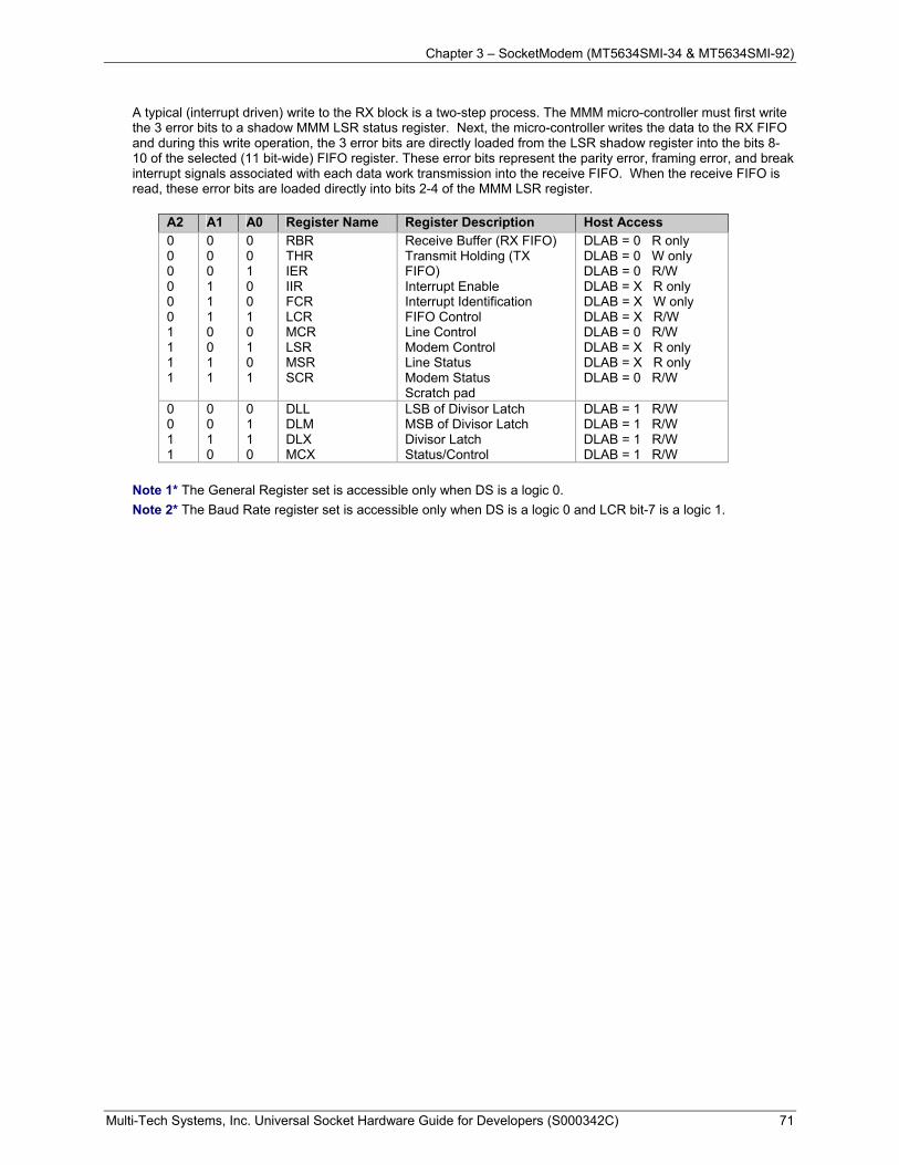
Chapter 3 – SocketModem (MT5634SMI-34 & MT5634SMI-92)
Multi-Tech Systems, Inc. Universal Socket Hardware Guide for Developers (S000342C) 71
A typical (interrupt driven) write to the RX block is a two-step process. The MMM micro-controller must first write the 3 error bits to a shadow MMM LSR status register. Next, the micro-controller writes the data to the RX FIFO and during this write operation, the 3 error bits are directly loaded from the LSR shadow register into the bits 8-10 of the selected (11 bit-wide) FIFO register. These error bits represent the parity error, framing error, and break interrupt signals associated with each data work transmission into the receive FIFO. When the receive FIFO is read, these error bits are loaded directly into bits 2-4 of the MMM LSR register.
A2 A1 A0 Register Name Register Description Host Access 0 0 0 0 0 0 1 1 1 1
0 0 0 1 1 1 0 0 1 1
0 0 1 0 0 1 0 1 0 1
RBR THR IER IIR FCR LCR MCR LSR MSR SCR
Receive Buffer (RX FIFO) Transmit Holding (TX FIFO) Interrupt Enable Interrupt Identification FIFO Control Line Control Modem Control Line Status Modem Status Scratch pad
DLAB = 0 R only DLAB = 0 W only DLAB = 0 R/W DLAB = X R only DLAB = X W only DLAB = X R/W DLAB = 0 R/W DLAB = X R only DLAB = X R only DLAB = 0 R/W
0 0 1 1
0 0 1 0
0 1 1 0
DLL DLM DLX MCX
LSB of Divisor Latch MSB of Divisor Latch Divisor Latch Status/Control
DLAB = 1 R/W DLAB = 1 R/W DLAB = 1 R/W DLAB = 1 R/W
Note 1* The General Register set is accessible only when DS is a logic 0. Note 2* The Baud Rate register set is accessible only when DS is a logic 0 and LCR bit-7 is a logic 1.
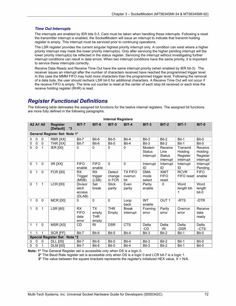
Chapter 3 – SocketModem (MT5634SMI-34 & MT5634SMI-92)
Multi-Tech Systems, Inc. Universal Socket Hardware Guide for Developers (S000342C) 72
Time Out Interrupts The interrupts are enabled by IER bits 0-3. Care must be taken when handling these interrupts. Following a reset the transmitter interrupt is enabled, the SocketModem will issue an interrupt to indicate that transmit holding register is empty. This interrupt must be serviced prior to continuing operations. The LSR register provides the current singular highest priority interrupt only. A condition can exist where a higher priority interrupt may mask the lower priority interrupt(s). Only after servicing the higher pending interrupt will the lower priority interrupt(s) be reflected in the status register. Servicing the interrupt without investigating further interrupt conditions can result in data errors. When two interrupt conditions have the same priority, it is important to service these interrupts correctly. Receive Data Ready and Receive Time Out have the same interrupt priority (when enabled by IER bit-3). The receiver issues an interrupt after the number of characters received have reached the programmed trigger level. In this case the MMM FIFO may hold more characters than the programmed trigger level. Following the removal of a data byte, the user should recheck LSR bit-0 for additional characters. A Receive Time Out will not occur if the receive FIFO is empty. The time out counter is reset at the center of each stop bit received or each time the receive holding register (RHR) is read.
Register Functional Definitions The following table delineates the assigned bit functions for the twelve internal registers. The assigned bit functions are more fully defined in the following paragraphs.
Internal Registers A2 A1 A0 Register
[Default] *3 BIT-7 BIT-6 BIT-5 BIT-4 BIT-3 BIT-2 BIT-1 BIT-0
General Register Set: Note 1* 0 0 0 RBR [XX] Bit-7 Bit-6 Bit-5 Bit-4 Bit-3 Bit-2 Bit-1 Bit-0 0 0 0 THR [XX] Bit-7 Bit-6 Bit-5 Bit-4 Bit-3 Bit-2 Bit-1 Bit-0 0 0 1 IER [00] 0 0 0 0 Modem
Status Interrupt
Receive Line Status interrupt
Transmit Holding Register interrupt
Receive Holding Register interrupt
0 1 0 IIR [XX] FIFO enable
FIFO enable
0 0 Interrupt ID
Interrupt ID
Interrupt ID
Interrupt Pending
0 1 0 FCR [00] RX Trigger (MSB)
RX trigger (LSB)
Detect change in FCR
TX FIFO overrun bit
DMA mode select
XMIT FIFO reset
RCVR FIFO reset
FIFO enable
0 1 1 LCR [00] Divisor latch access (DLAB)
Set break
Stick parity
Even parity
Parity enable
0 Word length bit-1
Word length bit-0
1 0 0 MCR [00] 0 0 0 Loop back
INT enable
OUT 1 -RTS -DTR
1 0 1 LSR [60] RX FIFO data error
TX empty THR empty
THR Empty
Break interrupt
Framing error
Parity error
Overrun error
Receive data ready
1 1 0 MSR [X0] CD RI
DSR
CTS Delta -CD
Delta -RI
Delta -DSR
Delta -CTS
1 1 1 SCR [FF] Bit-7 Bit-6 Bit-5 Bit-4 Bit-3 Bit-2 Bit-1 Bit-0 Special Register Set: Note *2 0 0 0 DLL [00] Bit-7 Bit-6 Bit-5 Bit-4 Bit-3 Bit-2 Bit-1 Bit-0 0 0 1 DLM [00] Bit-7 Bit-6 Bit-5 Bit-4 Bit-3 Bit-2 Bit-1 Bit-0
Note: 1* The General Register set is accessible only when DS is a logic 0. 2* The Baud Rate register set is accessible only when DS is a logic 0 and LCR bit-7 is a logic 1. 3* The value between the square brackets represents the register's initialized HEX value, X = N/A.
Chapter 3 – SocketModem (MT5634SMI-34 & MT5634SMI-92)
Multi-Tech Systems, Inc. Universal Socket Hardware Guide for Developers (S000342C) 73
RBR – Receive Buffer (RX FIFO) All eight bits are used for receive channel data (host read/data in; host write/data out). The three error bits per byte are copied into bits 2, 3, and 4 of the LSR during each host I/O read; therefore, they are available for monitoring on a per-byte basis.
THR – Transmit Holding Register (TX FIFO) All eight bits are used for transmit channel data (host write/data out; host read/data in).
IER – Interrupt Enable Bits 4–7: Reserved and will always read 0. Bits 0-3: Set by host software only and cleared by software control or host reset. Bit 3: Enables modem status IRQ. If bits 0–3 of the MSR are set and this bit is set to 1 (enabled),
a host interrupt is generated. Bit 2: Enables receive line status IRQ. If bits 1–4 (overrun, parity, framing, break errors) of the
LSR are set and this bit is set to a logic 1, a host interrupt is generated. Bit 1: Enables transmit holding register IRQ. If bit 5 (transmit holding register empty) of the LSR is
set and this bit is set to a 1, a host interrupt is generated. Bit 0: Enables received data available IRQ. If bit 0 (data ready) of the LSR is set and this bit is set
to a 1, a host interrupt is generated.
IIR – Interrupt Identification (Read Only) Bits 6–7: (FIFO enabled bits). These bits will read a 1 if FIFO mode is enabled and the 16450 enable
bit is 0 (no force of 16450 mode). Bits 4–5: Reserved and always read a 0. Bits 1–3: Interrupt ID bits. Bit 0: Interrupt pending. If logic 0 (in default mode), an interrupt is pending.
When the host accesses IIR, the contents of the register are frozen. Any new interrupts will be recorded, but not acknowledged during the IIR access. This requires buffering bits (0–3, 6–7) during IIR reads.
Interrupt Sources and Reset Control Table Bit 3 Bit 2 Bit 1 Priority Interrupt Source Interrupt Reset Control
0 1 1 Highest Overrun, parity, framing, error
or break detect bits set by SocketModem Controller
Reading the LSR
0 1 0 2nd Received data trigger level
RX FIFO drops below trigger level
1 1 0 2nd Receiver time-out with data in RX FIFO
Read RX FIFO
0 0 1 3rd TX holding register empty Writing to TX holding register or reading IIR when TX holding register is source of error
0 0 0 4th MODEM status: CTS, DSR, RI or DCD
Reading the MSR
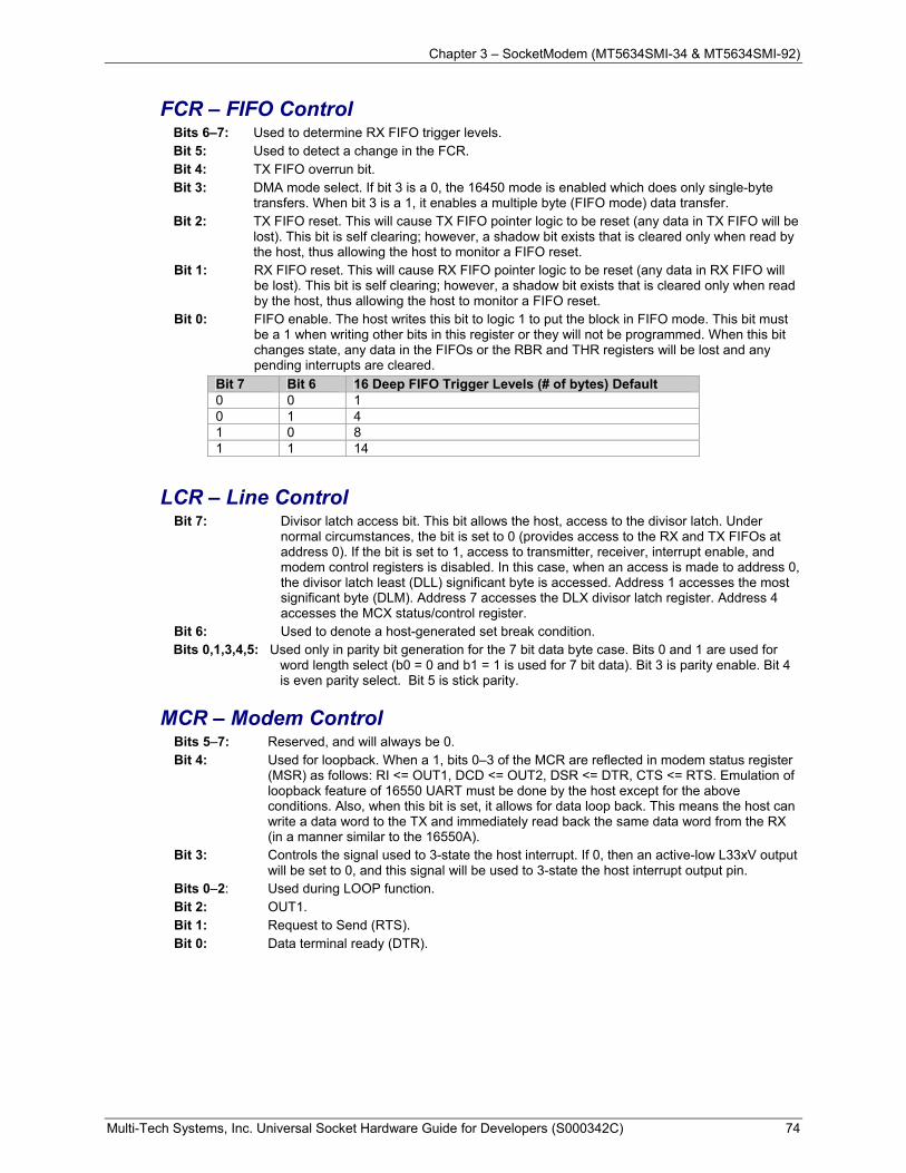
Chapter 3 – SocketModem (MT5634SMI-34 & MT5634SMI-92)
Multi-Tech Systems, Inc. Universal Socket Hardware Guide for Developers (S000342C) 74
FCR – FIFO Control Bits 6–7: Used to determine RX FIFO trigger levels. Bit 5: Used to detect a change in the FCR. Bit 4: TX FIFO overrun bit. Bit 3: DMA mode select. If bit 3 is a 0, the 16450 mode is enabled which does only single-byte
transfers. When bit 3 is a 1, it enables a multiple byte (FIFO mode) data transfer. Bit 2: TX FIFO reset. This will cause TX FIFO pointer logic to be reset (any data in TX FIFO will be
lost). This bit is self clearing; however, a shadow bit exists that is cleared only when read by the host, thus allowing the host to monitor a FIFO reset.
Bit 1: RX FIFO reset. This will cause RX FIFO pointer logic to be reset (any data in RX FIFO will be lost). This bit is self clearing; however, a shadow bit exists that is cleared only when read by the host, thus allowing the host to monitor a FIFO reset.
Bit 0: FIFO enable. The host writes this bit to logic 1 to put the block in FIFO mode. This bit must be a 1 when writing other bits in this register or they will not be programmed. When this bit changes state, any data in the FIFOs or the RBR and THR registers will be lost and any pending interrupts are cleared.
Bit 7 Bit 6 16 Deep FIFO Trigger Levels (# of bytes) Default 0 0 1 0 1 4 1 0 8 1 1 14
LCR – Line Control Bit 7: Divisor latch access bit. This bit allows the host, access to the divisor latch. Under
normal circumstances, the bit is set to 0 (provides access to the RX and TX FIFOs at address 0). If the bit is set to 1, access to transmitter, receiver, interrupt enable, and modem control registers is disabled. In this case, when an access is made to address 0, the divisor latch least (DLL) significant byte is accessed. Address 1 accesses the most significant byte (DLM). Address 7 accesses the DLX divisor latch register. Address 4 accesses the MCX status/control register.
Bit 6: Used to denote a host-generated set break condition. Bits 0,1,3,4,5: Used only in parity bit generation for the 7 bit data byte case. Bits 0 and 1 are used for
word length select (b0 = 0 and b1 = 1 is used for 7 bit data). Bit 3 is parity enable. Bit 4 is even parity select. Bit 5 is stick parity.
MCR – Modem Control Bits 5–7: Reserved, and will always be 0. Bit 4: Used for loopback. When a 1, bits 0–3 of the MCR are reflected in modem status register
(MSR) as follows: RI <= OUT1, DCD <= OUT2, DSR <= DTR, CTS <= RTS. Emulation of loopback feature of 16550 UART must be done by the host except for the above conditions. Also, when this bit is set, it allows for data loop back. This means the host can write a data word to the TX and immediately read back the same data word from the RX (in a manner similar to the 16550A).
Bit 3: Controls the signal used to 3-state the host interrupt. If 0, then an active-low L33xV output will be set to 0, and this signal will be used to 3-state the host interrupt output pin.
Bits 0–2: Used during LOOP function. Bit 2: OUT1. Bit 1: Request to Send (RTS). Bit 0: Data terminal ready (DTR).
Chapter 3 – SocketModem (MT5634SMI-34 & MT5634SMI-92)
Multi-Tech Systems, Inc. Universal Socket Hardware Guide for Developers (S000342C) 75
LSR – Line Status Bit 7: Error in RX FIFO. This bit is always set to 1 if at least one data byte in the RX FIFO has an
error. This will clear when there are no more errors in the RX FIFO. Bit 6: Transmitter empty. This bit is the same as LSR bit 5 (THRE) in MMM Bit 5: Transmitter holding register empty. This bit is set to 1 when either the transmitter holding
register has been read (emptied) by the micro-controller (16450 mode) or the TX FIFO is empty (16550 mode). This bit is set to 0 when either the THR or the TX FIFO becomes not empty in 16450 mode. In 16550 mode, it is set to 0 only after the trigger level has been met since the last occurrence of TX FIFO empty. If the transmitter timer is enabled, a shadow bit exists which delays the timer setting this bit to 1. When reading this bit, the micro-controller will not see the delay. Both shadow and register bits are cleared when the host writes to the THR or TX FIFO in 16450 mode. The trigger level must be reached to clear the bit in 16550 (FIFO) mode.
Bits 2–4: Used for parity error, framing error, and break detect. These bits are written, indirectly, by the micro-controller as follows: The bits are first written to the shadow bit locations when the micro-controller write accesses the LSR. When the next character is written to the receive buffer (RBR) or the RX FIFO, the data in the shadow bits is then copied to the RBR (16450 mode) or RX FIFO (16550 mode). In FIFO mode, bits become available to the host when the data byte associated with the bits is next to be read. In FIFO mode, with successive reads of the receiver, the status bits will be set if an error occurs on any byte. Once the micro-controller writes to the RBR or RX FIFO, the shadow bits are auto cleared. The register bits are updated with each host read.
Bit 1: Overrun error. This bit is set if the micro-controller makes a second write to RBR before the host reads data in the buffer (16450 mode) or with a full RX FIFO (16550 mode). No data will be transferred to the RX FIFO under these circumstances. This bit is reset when the host reads the LSR.
Bit 0: Data ready bit. This bit is set to 1 when received data is available, either in the RX FIFO (16550 mode) or the RBR (16450 mode). This bit is set immediately upon the micro-controller writing data to the RBR or FIFO if the receive timer is not enabled, but it is delayed by the timer interval if the receive timer is enabled. For micro-controller read access, a shadow bit exists so that the micro-controller does not see the delay that the host sees. Both bits are cleared to logic 0 immediately upon reading all data in either RBR or RX FIFO.
MSR – Modem Status Bits 4 through 7 of the MSR can also take on the MCR bits 0 through 3 value when in MCR loop mode (i.e. when MCR b4 = 1). The transfer of bits in loop back has a null modem twist (i.e. MCR b0 goes to MSR b5 and MCR b1goes to MSR b4).
Bit 7: Data carrier detect (DCD) bit. Bit 6: Ring indicator (RI) bit. Bit 5: Data set ready (DSR) bit. Bit 4: Clear to send (CTS) bit. Bit 3: Delta data carrier detect pin. This bit is set to a 1 whenever the data carrier detect bit changes
state. It is reset when the host reads the modem status register. Bit 2: Trailing edge ring indicator bit. This bit is set to 1 on the falling edge of the ring indicator bit. It
is reset when the host reads the modem status register. Bit 1: Delta data set ready bit. This bit is set to 1 whenever the data set ready changes state. It is
reset when the host reads the modem status register. Bit 0: Delta clear to send bit. This bit is a one whenever the clear to send bit changes state. It is reset
when the host reads the modem status register.
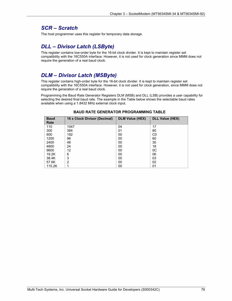
Chapter 3 – SocketModem (MT5634SMI-34 & MT5634SMI-92)
Multi-Tech Systems, Inc. Universal Socket Hardware Guide for Developers (S000342C) 76
SCR – Scratch The host programmer uses this register for temporary data storage.
DLL – Divisor Latch (LSByte) This register contains low-order byte for the 16-bit clock divider. It is kept to maintain register set compatibility with the 16C550A interface. However, it is not used for clock generation since MMM does not require the generation of a real baud clock.
DLM – Divisor Latch (MSByte) This register contains high-order byte for the 16-bit clock divider. It is kept to maintain register set compatibility with the 16C550A interface. However, it is not used for clock generation, since MMM does not require the generation of a real baud clock.
Programming the Baud Rate Generator Registers DLM (MSB) and DLL (LSB) provides a user capability for selecting the desired final baud rate. The example in the Table below shows the selectable baud rates available when using a 1.8432 MHz external clock input.
BAUD RATE GENERATOR PROGRAMMING TABLE Baud Rate
16 x Clock Divisor (Decimal) DLM Value (HEX) DLL Value (HEX)
110 300 600 1200 2400 4800 9600 19.2K 38.4K 57.6K 115.2K
1047 384 192 96 48 24 12 6 3 2 1
04 01 00 00 00 00 00 00 00 00 00
17 80 C0 60 30 18 0C 06 03 02 01
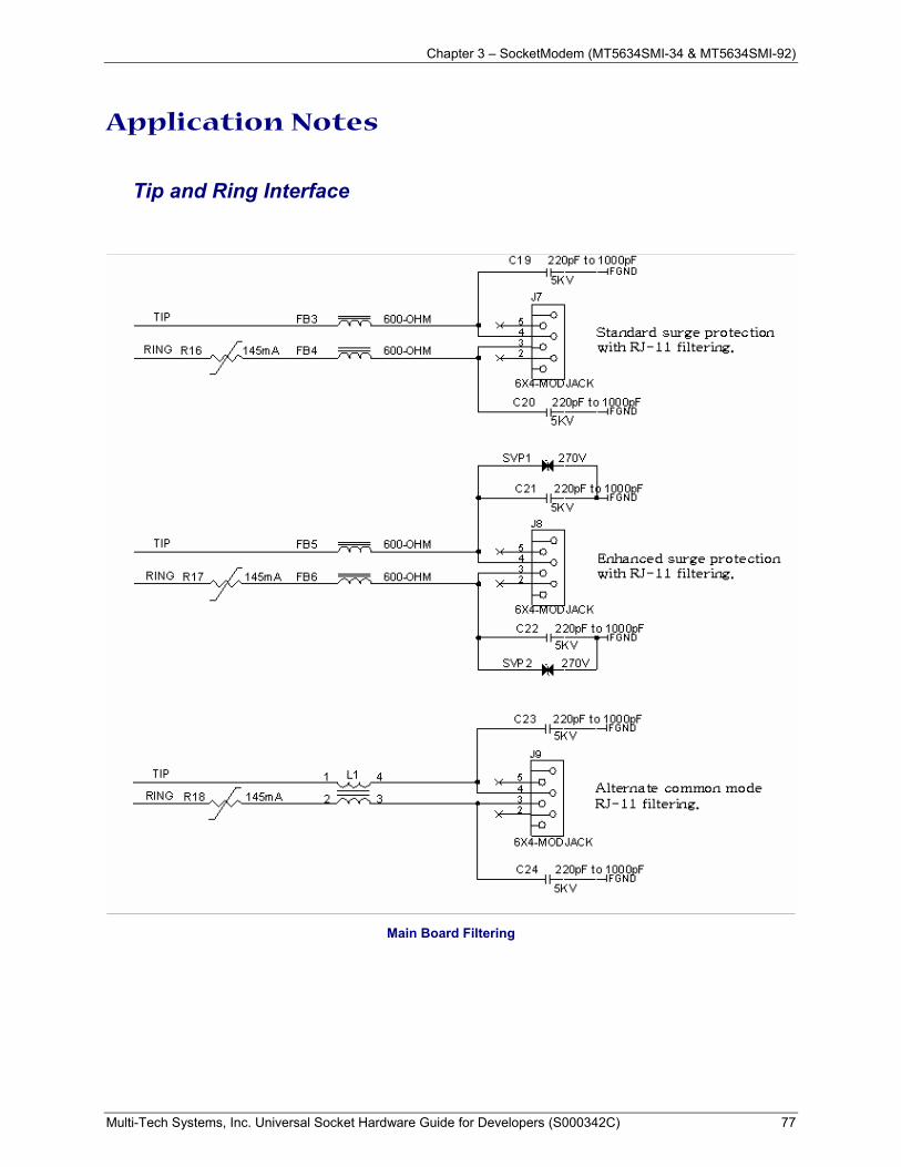
Chapter 3 – SocketModem (MT5634SMI-34 & MT5634SMI-92)
Multi-Tech Systems, Inc. Universal Socket Hardware Guide for Developers (S000342C) 77
Application Notes
Tip and Ring Interface
Main Board Filtering
Chapter 3 – SocketModem (MT5634SMI-34 & MT5634SMI-92)
Multi-Tech Systems, Inc. Universal Socket Hardware Guide for Developers (S000342C) 78
Recommended Parts Disclaimer: Multi-Tech Systems makes no warranty claims for vendor product recommendations listed below. Other vendor products may or may not operate satisfactorily. Multi-Tech System’s recommended vendor products only indicate that the product has been tested in controlled conditions and were found to perform satisfactorily.
Surface mount ferrites are used on T&R (Tip and Ring) to mitigate emission levels out the RJ-11 cable. 220pF capacitors are also used on T&R to reduce the common mode emissions that may be present in certain systems. The ferrite and capacitors also aid in reducing the effects of transients that may be present on the line.
Recommended Ferrite (SMT) Manufacturer – Associated Component Technology (ACT) – Part # - YCB-1206 Manufacturer – Murata Erie – Part # - BLM31AJ601SN1
Recommended Ferrite (Thru-Hole) Manufacturer – Associated Component Technology (ACT) – Part # - WB2-2.OT
Recommended Capacitor Manufacturer – NOVACAP – Part # - ES2211NKES502NXT Manufacturer – Murata Erie – Part # - GA355DR7GC221KY02L (Surface mount device)
Part # - DE0807B221K-KH (Thru-hole device) Manufacturer – Ever Grace Electronic Industrials -- Part # - YP221K2EA7PS Note: The capacitors used on T&R must have a Y2 safety rating.
Recommended Connector Manufacturer – Stewart – Part # - SS-6446-NF-A431
Recommended Poly Switch Thermal Fuse (can be reset) Manufacturer – RayChem – Part # - TS600-170 Note: The fuse is also needed to meet UL60950 for protection against over-voltage from power line crosses.
Telecom The RJ-11 connector must meet FCC Part 68 requirements. Refer to FCC Part 68 section 68.500 subpart F for connector specifications. A self-healing fuse is used in series with line to help prevent damage to the DAA circuit. This fuse is needed for FCC Part 68 compliance.
Common Mode Choke Manufacturer – TDK – Part # - ZJYS51R5-2PT
Recommended Sidactor Manufacturer – Teccor Electronics – Part # - P#3100SA Manufacturer – ST Microelectronics -- Part 1 – SMP100LC-270
Recommended Transceiver Manufacturer – Analog Devices – Part # - ADM207EAR
Multi-Tech Systems, Inc. Universal Socket Hardware Guide for Developers (S000342C) 79
Chapter 4
SocketModem
MT2456SMI-22
Chapter 4 – SocketModem (MT2456SMI-22)
Multi-Tech Systems, Inc. Universal Socket Hardware Guide for Developers (S000342C) 80
Chapter 4 – SocketModem (MT2456SMI-22)
Introduction The Multi-Tech SocketModem supports analog data modem operation with V.22bis Fast Connect, V.42bis data compression, and V.80 synchronous access mode. The SocketModem is a space-efficient (1" × 2.5"), embedded modem that is ready-to-integrate into your applications; therefore, dramatically reducing development time and costs for system designers.
The MT2456SMI-22 SocketModem is a standard 64-pin modem used for integrating data communications. It is a single-port 5 V or 3.3 V modem that integrates a modem controller, DSP, and DAA in a 1" x 2.5" form factor and communicates to a host controller via an asynchronous serial interface.
Product Ordering Information Product Description Region Order this
Product
MT2456SMI-22 V.22bis Serial Data Only – 5 V Global MT2456SMI-L22 V.22bis Serial Data Only – 3.3 V Global
Telecom Label MT2456SMI-LS MT2456SMI-Global Regulatory Label Global
Developer Kit MTSMI-DK SocketModem Serial Developer Kit Global
How to Read the Product Codes in the Table Above:
22 5 Volt Build L22 3.3 Volt Build LS Telecom Label DK
Developer Kit A SocketModem Developer Kit is available for the MT2456SMI-22. It includes one developer board with an RS-232 DB-25 connector, wall power adapter, RJ-11 jack, an RS-232 cable, and a Developer Kit CD.
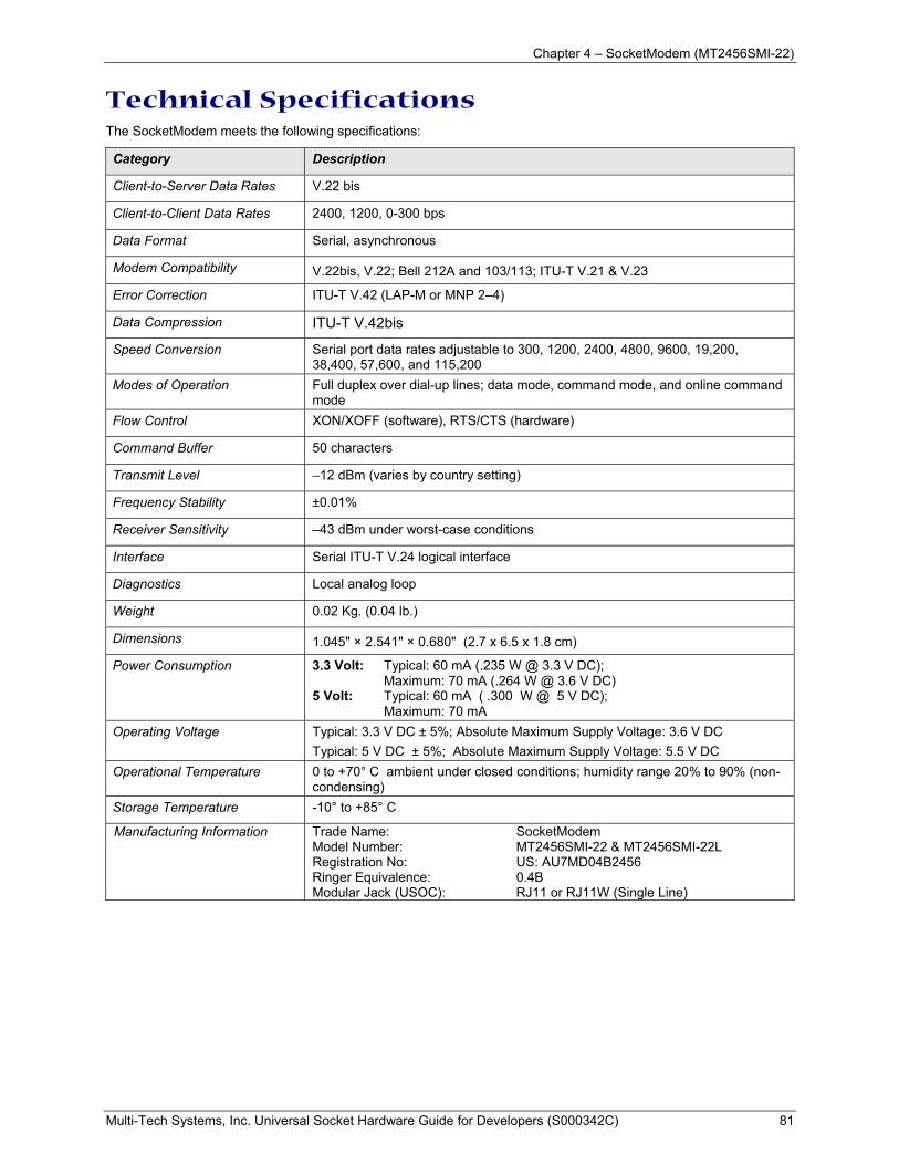
Chapter 4 – SocketModem (MT2456SMI-22)
Multi-Tech Systems, Inc. Universal Socket Hardware Guide for Developers (S000342C) 81
Technical Specifications The SocketModem meets the following specifications:
Category Description
Client-to-Server Data Rates V.22 bis
Client-to-Client Data Rates 2400, 1200, 0-300 bps
Data Format Serial, asynchronous
Modem Compatibility V.22bis, V.22; Bell 212A and 103/113; ITU-T V.21 & V.23
Error Correction ITU-T V.42 (LAP-M or MNP 2–4)
Data Compression ITU-T V.42bis
Speed Conversion Serial port data rates adjustable to 300, 1200, 2400, 4800, 9600, 19,200, 38,400, 57,600, and 115,200
Modes of Operation Full duplex over dial-up lines; data mode, command mode, and online command mode
Flow Control XON/XOFF (software), RTS/CTS (hardware)
Command Buffer 50 characters
Transmit Level –12 dBm (varies by country setting)
Frequency Stability ±0.01%
Receiver Sensitivity –43 dBm under worst-case conditions
Interface Serial ITU-T V.24 logical interface
Diagnostics Local analog loop
Weight 0.02 Kg. (0.04 lb.)
Dimensions 1.045" × 2.541" × 0.680" (2.7 x 6.5 x 1.8 cm)
Power Consumption 3.3 Volt: Typical: 60 mA (.235 W @ 3.3 V DC); Maximum: 70 mA (.264 W @ 3.6 V DC)
5 Volt: Typical: 60 mA ( .300 W @ 5 V DC); Maximum: 70 mA
Operating Voltage Typical: 3.3 V DC ± 5%; Absolute Maximum Supply Voltage: 3.6 V DC Typical: 5 V DC ± 5%; Absolute Maximum Supply Voltage: 5.5 V DC
Operational Temperature 0 to +70° C ambient under closed conditions; humidity range 20% to 90% (non-condensing)
Storage Temperature -10° to +85° C
Manufacturing Information Trade Name: SocketModem Model Number: MT2456SMI-22 & MT2456SMI-22L Registration No: US: AU7MD04B2456 Ringer Equivalence: 0.4B Modular Jack (USOC): RJ11 or RJ11W (Single Line)
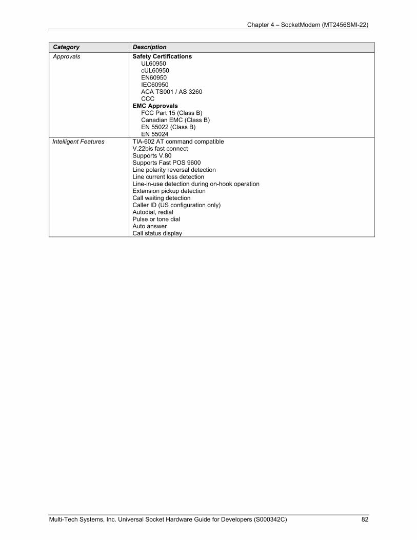
Chapter 4 – SocketModem (MT2456SMI-22)
Multi-Tech Systems, Inc. Universal Socket Hardware Guide for Developers (S000342C) 82
Category Description Approvals Safety Certifications
UL60950 cUL60950 EN60950 IEC60950 ACA TS001 / AS 3260 CCC
EMC Approvals FCC Part 15 (Class B) Canadian EMC (Class B) EN 55022 (Class B) EN 55024
Intelligent Features TIA-602 AT command compatible V.22bis fast connect Supports V.80 Supports Fast POS 9600 Line polarity reversal detection Line current loss detection Line-in-use detection during on-hook operation Extension pickup detection Call waiting detection Caller ID (US configuration only) Autodial, redial Pulse or tone dial Auto answer Call status display
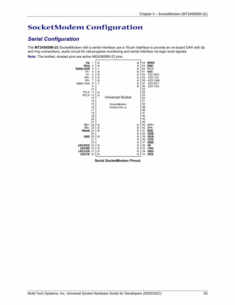
Chapter 4 – SocketModem (MT2456SMI-22)
Multi-Tech Systems, Inc. Universal Socket Hardware Guide for Developers (S000342C) 83
SocketModem Configuration
Serial Configuration The MT2456SMI-22 SocketModem with a serial interface use a 16-pin interface to provide an on-board DAA with tip and ring connections, audio circuit for call-progress monitoring and serial interface via logic level signals. Note: The bolded, shaded pins are active Mt2456SMI-22 pins.
Serial SocketModem Pinout
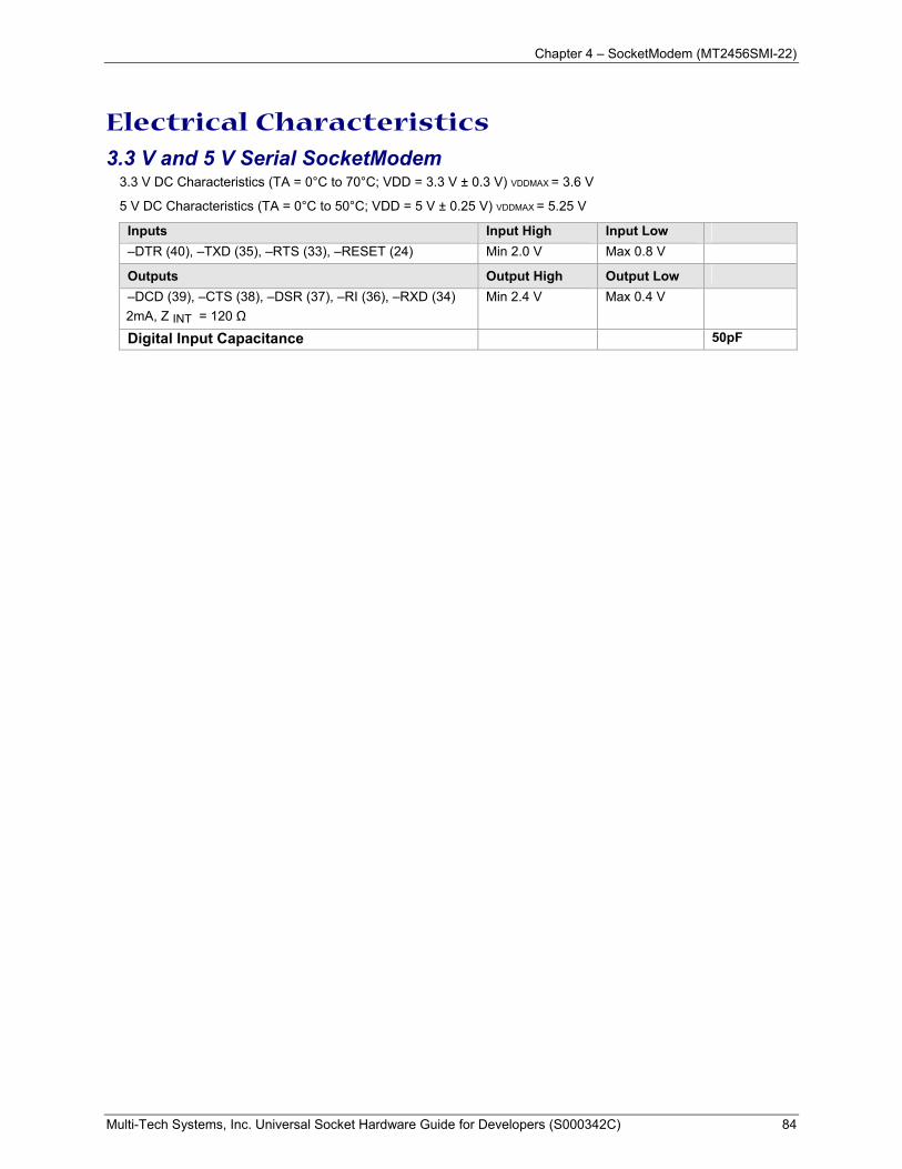
Chapter 4 – SocketModem (MT2456SMI-22)
Multi-Tech Systems, Inc. Universal Socket Hardware Guide for Developers (S000342C) 84
Electrical Characteristics
3.3 V and 5 V Serial SocketModem 3.3 V DC Characteristics (TA = 0°C to 70°C; VDD = 3.3 V ± 0.3 V) VDDMAX = 3.6 V
5 V DC Characteristics (TA = 0°C to 50°C; VDD = 5 V ± 0.25 V) VDDMAX = 5.25 V
Inputs Input High Input Low –DTR (40), –TXD (35), –RTS (33), –RESET (24) Min 2.0 V Max 0.8 V
Outputs Output High Output Low
–DCD (39), –CTS (38), –DSR (37), –RI (36), –RXD (34) 2mA, Z INT = 120 Ω
Min 2.4 V Max 0.4 V
Digital Input Capacitance 50pF
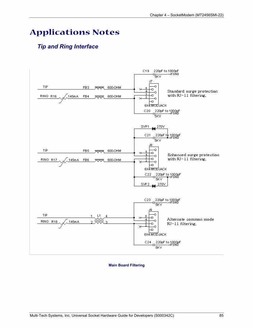
Chapter 4 – SocketModem (MT2456SMI-22)
Multi-Tech Systems, Inc. Universal Socket Hardware Guide for Developers (S000342C) 85
Applications Notes
Tip and Ring Interface
Main Board Filtering

Chapter 4 – SocketModem (MT2456SMI-22)
Multi-Tech Systems, Inc. Universal Socket Hardware Guide for Developers (S000342C) 86
Recommended Parts Disclaimer: Multi-Tech Systems makes no warranty claims for vendor product recommendations listed below. Other vendor products may or may not operate satisfactorily. Multi-Tech System’s recommended vendor products only indicate that the product has been tested in controlled conditions and were found to perform satisfactorily.
Surface mount ferrites are used on T&R (Tip and Ring) to mitigate emission levels out the RJ-11 cable. 220pF capacitors are also used on T&R to reduce the common mode emissions that may be present in certain systems. The ferrite and capacitors also aid in reducing the effects of transients that may be present on the line.
Recommended Ferrite (SMT) Manufacturer – Associated Component Technology (ACT) – Part # - YCB-1206 Manufacturer – Murata Erie – Part # - BLM31AJ601SN1
Recommended Ferrite (Thru-Hole) Manufacturer – Associated Component Technology (ACT) – Part # - WB2-2.OT
Recommended Capacitor Manufacturer – NOVACAP – Part # - ES2211NKES502NXT Manufacturer – Murata Erie – Part # - GA355DR7GC221KY02L (Surface mount device)
Part # - DE0807B221K-KH (Thru-hole device) Manufacturer – Ever Grace Electronic Industrials -- Part # - YP221K2EA7PS Note: The capacitors used on T&R must have a Y2 safety rating.
Recommended Connector Manufacturer – Stewart – Part # - SS-6446-NF-A431
Recommended Poly Switch Thermal Fuse (can be reset) Manufacturer – RayChem – Part # - TS600-170 Note: The fuse is also needed to meet UL60950 for protection against over-voltage from power line crosses.
Telecom The RJ-11 connector must meet FCC Part 68 requirements. Refer to FCC Part 68 section 68.500 subpart F for connector specifications. A self-healing fuse is used in series with line to help prevent damage to the DAA circuit. This fuse is needed for FCC Part 68 compliance.
Common Mode Choke Manufacturer – TDK – Part # - ZJYS51R5-2PT
Recommended Sidactor Manufacturer – Teccor Electronics – Part # - P#3100SA Manufacturer – ST Microelectronics -- Part 1 – SMP100LC-270
Recommended Transceiver Manufacturer – Analog Devices – Part # - ADM207EAR
Multi-Tech Systems, Inc. Universal Socket Hardware Guide for Developers (S000342C) 87
Chapter 5
SocketModem IP
MT2456SMI-IP
Chapter 5 – SocketModem IP (MT2456SMI-IP)
Multi-Tech Systems, Inc. Universal Socket Hardware Guide for Developers (S000342C) 88
Chapter 5 – SocketModem IP (MT2456SMI-IP)
Introduction The Multi-Tech SocketModem IP integrates dial-up PSTN modem functionality and a complete TCP/IP protocol stack into a single product design.
The SocketModem IP is a complete ready-to-integrate module that embeds Internet protocols inside your product device allowing it to send and receive data over the Internet without connecting to a PC or gateway server.
The space efficient (1” x 2.5”) embedded modem of the SocketModem IP sends and receives data via e-mail, HTTP, or socket interfaces.
The SocketModem IP has successfully completed international compliance testing (homologation) for global approval. This means you can specify one module for each system used across the world. And, since the SocketModem IP is a host independent device, the associated telecom approvals are portable across any solution for which it is integrated.
Product Ordering Information Product Description Region Order this
Product
MT2456SMI-IP-L22 V.22bis/2400 SocketModem and IP – 3.3 V Global MT2456SMI-IP-L32 V.32bis/14.4K SocketModem and IP – 3.3 V Global MT2456SMI-IP-L34 V.34/33.6K SocketModem and IP – 3.3 V Global MT2456SMI-IP-L92 V.92/56K SocketModem and IP – 3.3 V Global
Telecom Label MT2456SMI-LS MT2456SMI-Global Regulatory Label Global
Developer Kit MTSMI-DK SocketModem Serial Developer Kit Global
Developer Kit The SocketModem IP Developer Kit allows you to plug in the SocketModem IP and use it externally connected to your PC for testing, programming and evaluation.
The kit includes one: • One SocketModem IP module • A developer board • A universal power supply • An RS-232 cable • A Developer Kit CD
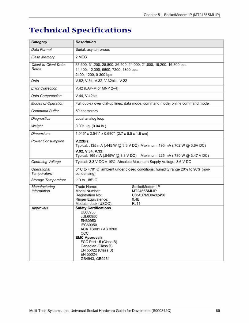
Chapter 5 – SocketModem IP (MT2456SMI-IP)
Multi-Tech Systems, Inc. Universal Socket Hardware Guide for Developers (S000342C) 89
Technical Specifications Category Description
Data Format Serial, asynchronous
Flash Memory 2 MEG
Client-to-Client Data Rates
33,600, 31,200, 28,800, 26,400, 24,000, 21,600, 19,200, 16,800 bps 14,400, 12,000, 9600, 7200, 4800 bps 2400, 1200, 0-300 bps
Data V.92; V.34, V.32, V.32bis, V.22
Error Correction V.42 (LAP-M or MNP 2–4)
Data Compression V.44, V.42bis
Modes of Operation Full duplex over dial-up lines; data mode, command mode, online command mode
Command Buffer 50 characters
Diagnostics Local analog loop
Weight 0.001 kg. (0.04 lb.)
Dimensions 1.045" x 2.541" x 0.680" (2.7 x 6.5 x 1.8 cm)
Power Consumption V.22bis: Typical: .135 mA (.445 W @ 3.3 V DC); Maximum: 195 mA (.702 W @ 3.6V DC) V.92, V.34, V.32: Typical: 165 mA (.545W @ 3.3 V DC); Maximum: 225 mA (.780 W @ 3.47 V DC)
Operating Voltage Typical: 3.3 V DC ± 10%; Absolute Maximum Supply Voltage: 3.6 V DC
Operational Temperature
0° C to +70° C ambient under closed conditions; humidity range 20% to 90% (non-condensing)
Storage Temperature -10 to +85° C
Manufacturing Information
Trade Name: SocketModem IP Model Number: MT2456SMI-IP Registration No: US:AU7MD0432456 Ringer Equivalence: 0.4B Modular Jack (USOC): RJ11
Approvals Safety Certifications UL60950 cUL60950 EN60950 IEC60950 ACA TS001 / AS 3260 CCC
EMC Approvals FCC Part 15 (Class B) Canadian (Class B) EN 55022 (Class B) EN 55024 GB4943, GB9254
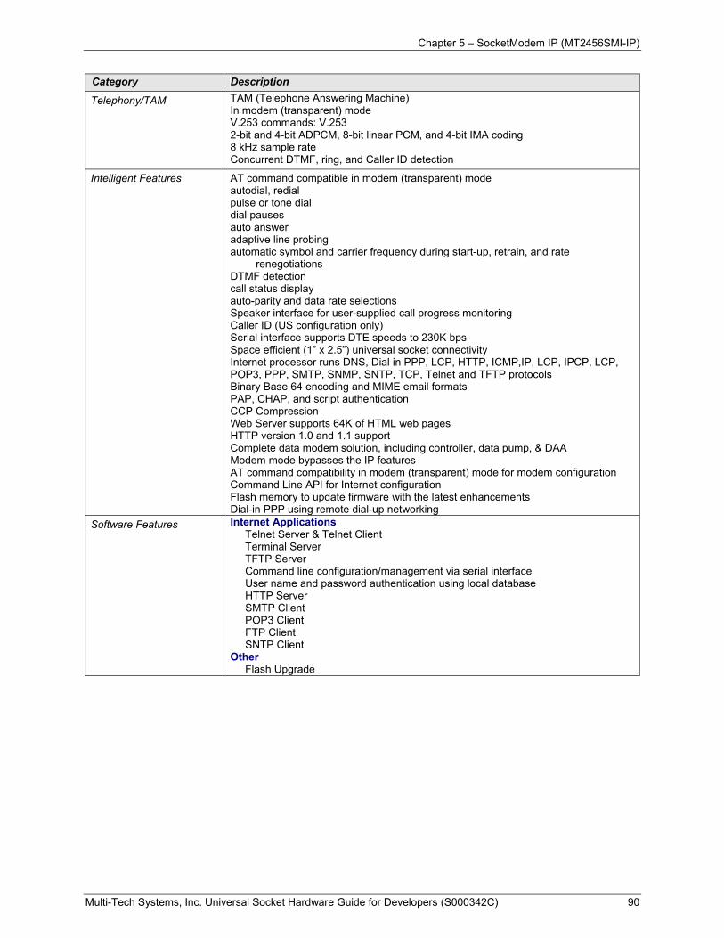
Chapter 5 – SocketModem IP (MT2456SMI-IP)
Multi-Tech Systems, Inc. Universal Socket Hardware Guide for Developers (S000342C) 90
Category Description
Telephony/TAM TAM (Telephone Answering Machine) In modem (transparent) mode V.253 commands: V.253 2-bit and 4-bit ADPCM, 8-bit linear PCM, and 4-bit IMA coding 8 kHz sample rate Concurrent DTMF, ring, and Caller ID detection
Intelligent Features
AT command compatible in modem (transparent) mode autodial, redial pulse or tone dial dial pauses auto answer adaptive line probing automatic symbol and carrier frequency during start-up, retrain, and rate
renegotiations DTMF detection call status display auto-parity and data rate selections Speaker interface for user-supplied call progress monitoring Caller ID (US configuration only) Serial interface supports DTE speeds to 230K bps Space efficient (1” x 2.5”) universal socket connectivity Internet processor runs DNS, Dial in PPP, LCP, HTTP, ICMP,IP, LCP, IPCP, LCP, POP3, PPP, SMTP, SNMP, SNTP, TCP, Telnet and TFTP protocols Binary Base 64 encoding and MIME email formats PAP, CHAP, and script authentication CCP Compression Web Server supports 64K of HTML web pages HTTP version 1.0 and 1.1 support Complete data modem solution, including controller, data pump, & DAA Modem mode bypasses the IP features AT command compatibility in modem (transparent) mode for modem configuration Command Line API for Internet configuration Flash memory to update firmware with the latest enhancements Dial-in PPP using remote dial-up networking
Software Features
Internet Applications Telnet Server & Telnet Client Terminal Server TFTP Server Command line configuration/management via serial interface User name and password authentication using local database HTTP Server SMTP Client POP3 Client FTP Client SNTP Client
Other Flash Upgrade
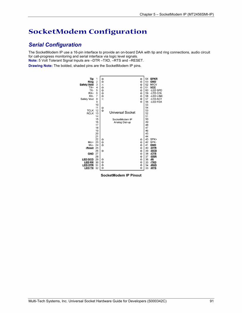
Chapter 5 – SocketModem IP (MT2456SMI-IP)
Multi-Tech Systems, Inc. Universal Socket Hardware Guide for Developers (S000342C) 91
SocketModem Configuration
Serial Configuration The SocketModem IP use a 16-pin interface to provide an on-board DAA with tip and ring connections, audio circuit for call-progress monitoring and serial interface via logic level signals. Note: 5 Volt Tolerant Signal Inputs are –DTR –TXD, –RTS and –RESET. Drawing Note: The bolded, shaded pins are the SocketModem IP pins.
SocketModem IP Pinout
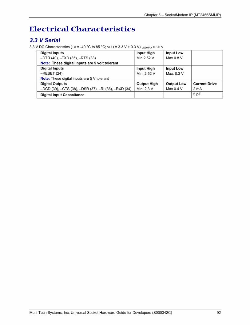
Chapter 5 – SocketModem IP (MT2456SMI-IP)
Multi-Tech Systems, Inc. Universal Socket Hardware Guide for Developers (S000342C) 92
Electrical Characteristics
3.3 V Serial 3.3 V DC Characteristics (TA = -40 °C to 85 °C; VDD = 3.3 V ± 0.3 V) VDDMAX = 3.6 V
Digital Inputs –DTR (40), –TXD (35), –RTS (33) Note: These digital inputs are 5 volt tolerant
Input High Min 2.52 V
Input Low Max 0.8 V
Digital Inputs –RESET (24) Note: These digital inputs are 5 V tolerant
Input High Min. 2.52 V
Input Low Max. 0.3 V
Digital Outputs –DCD (39), –CTS (38), –DSR (37), –RI (36), –RXD (34)
Output High Min. 2.3 V
Output Low Max 0.4 V
Current Drive 2 mA
Digital Input Capacitance 5 pF
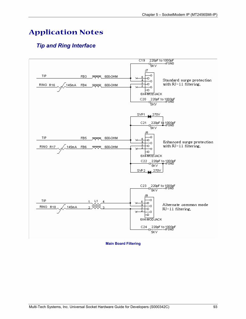
Chapter 5 – SocketModem IP (MT2456SMI-IP)
Multi-Tech Systems, Inc. Universal Socket Hardware Guide for Developers (S000342C) 93
Application Notes
Tip and Ring Interface
Main Board Filtering
Chapter 5 – SocketModem IP (MT2456SMI-IP)
Multi-Tech Systems, Inc. Universal Socket Hardware Guide for Developers (S000342C) 94
Recommended Parts Disclaimer: Multi-Tech Systems makes no warranty claims for vendor product recommendations listed below. Other vendor products may or may not operate satisfactorily. Multi-Tech System’s recommended vendor products only indicate that the product has been tested in controlled conditions and were found to perform satisfactorily.
Surface mount ferrites are used on T&R (Tip and Ring) to mitigate emission levels out the RJ-11 cable. 220pF capacitors are also used on T&R to reduce the common mode emissions that may be present in certain systems. The ferrite and capacitors also aid in reducing the effects of transients that may be present on the line.
Recommended Ferrite (SMT) Manufacturer – Associated Component Technology (ACT) – Part # - YCB-1206 Manufacturer – Murata Erie – Part # - BLM31AJ601SN1
Recommended Ferrite (Thru-Hole) Manufacturer – Associated Component Technology (ACT) – Part # - WB2-2.OT
Recommended Capacitor Manufacturer – NOVACAP – Part # - ES2211NKES502NXT Manufacturer – Murata Erie – Part # - GA355DR7GC221KY02L (Surface mount device)
Part # - DE0807B221K-KH (Thru-hole device) Manufacturer – Ever Grace Electronic Industrials -- Part # - YP221K2EA7PS Note: The capacitors used on T&R must have a Y2 safety rating.
Recommended Connector Manufacturer – Stewart – Part # - SS-6446-NF-A431
Recommended Poly Switch Thermal Fuse (can be reset) Manufacturer – RayChem – Part # - TS600-170 Note: The fuse is also needed to meet UL60950 for protection against over-voltage from power line crosses.
Telecom The RJ-11 connector must meet FCC Part 68 requirements. Refer to FCC Part 68 section 68.500 subpart F for connector specifications. A self-healing fuse is used in series with line to help prevent damage to the DAA circuit. This fuse is needed for FCC Part 68 compliance.
Common Mode Choke Manufacturer – TDK – Part # - ZJYS51R5-2PT
Recommended Sidactor Manufacturer – Teccor Electronics – Part # - P#3100SA Manufacturer – ST Microelectronics -- Part 1 – SMP100LC-270
Recommended Transceiver Manufacturer – Analog Devices – Part # - ADM207EAR
Multi-Tech Systems, Inc. Universal Socket Hardware Guide for Developers (S000342C) 95
Chapter 6
SocketEthernet IP
MTXCSEM
Chapter 6 – SocketEthernet IP (MTXCSEM)
Multi-Tech Systems, Inc. Universal Socket Hardware Guide for Developers (S000342C) 96
Chapter 6 – SocketEthernet IP (MTXCSEM)
Introduction The Multi-Tech SocketEthernet IP is a complete, ready to integrate serial-to-Ethernet module for connecting legacy devices to an IP network for remote monitoring, control and configuration. The space efficient module (1” x 2.5”) provides a high performance Ethernet bridge as well as a complete TCP/IP protocol stack into a single, universal socket design. The SocketEthernet IP can make your existing and next generation device, machine, or system, IP-ready while you focus on developing its core features.
Product Ordering Information Product Description Region Order this Product
MTXCSEM Serial to Ethernet + IP - 5 V Global MTXCSEM-L Serial to Ethernet + IP - 3.3 V Global
Developer Kit MTSEM-DK SocketEthernet IP Developer Kit Global
Developer Kit The SocketEthernet IP Developer Kit allows you to plug in the SocketEthernet IP and use it externally connected to your PC for testing, programming and evaluation.
The kit includes one: • One SocketEthernet IP module • A developer board • A universal power supply • An RS-232 cable • A Developer Kit CD
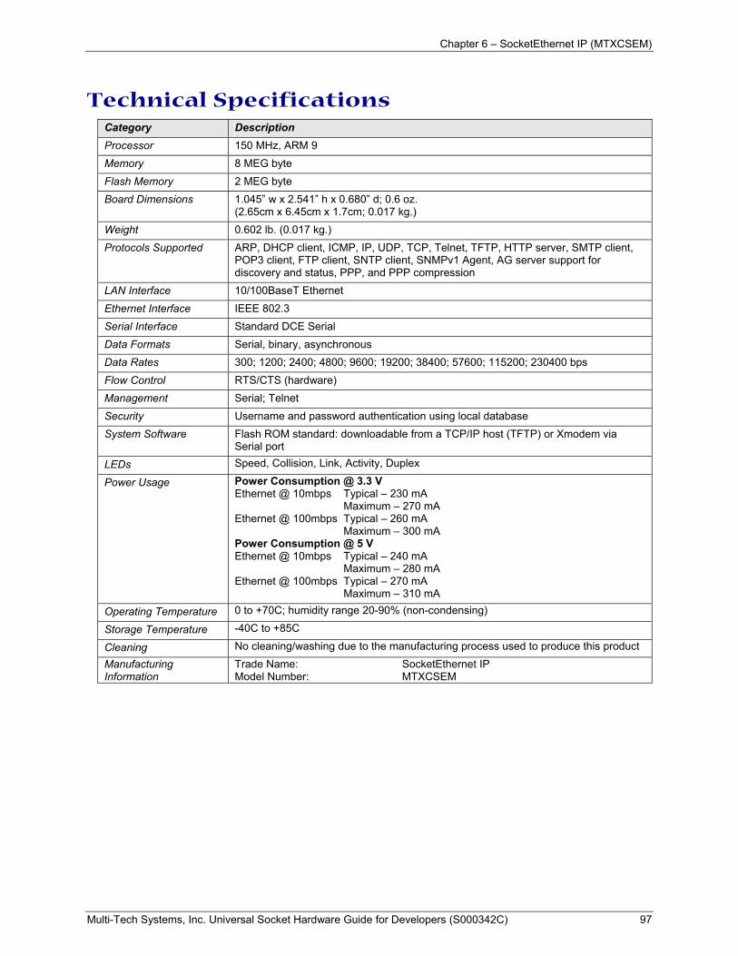
Chapter 6 – SocketEthernet IP (MTXCSEM)
Multi-Tech Systems, Inc. Universal Socket Hardware Guide for Developers (S000342C) 97
Technical Specifications Category Description Processor 150 MHz, ARM 9 Memory 8 MEG byte Flash Memory 2 MEG byte Board Dimensions 1.045” w x 2.541” h x 0.680” d; 0.6 oz.
(2.65cm x 6.45cm x 1.7cm; 0.017 kg.) Weight 0.602 lb. (0.017 kg.) Protocols Supported ARP, DHCP client, ICMP, IP, UDP, TCP, Telnet, TFTP, HTTP server, SMTP client,
POP3 client, FTP client, SNTP client, SNMPv1 Agent, AG server support for discovery and status, PPP, and PPP compression
LAN Interface 10/100BaseT Ethernet Ethernet Interface IEEE 802.3 Serial Interface Standard DCE Serial Data Formats Serial, binary, asynchronous Data Rates 300; 1200; 2400; 4800; 9600; 19200; 38400; 57600; 115200; 230400 bps Flow Control RTS/CTS (hardware) Management Serial; Telnet Security Username and password authentication using local database System Software Flash ROM standard: downloadable from a TCP/IP host (TFTP) or Xmodem via
Serial port LEDs Speed, Collision, Link, Activity, Duplex
Power Usage Power Consumption @ 3.3 V Ethernet @ 10mbps Typical – 230 mA Maximum – 270 mA Ethernet @ 100mbps Typical – 260 mA Maximum – 300 mA Power Consumption @ 5 V Ethernet @ 10mbps Typical – 240 mA Maximum – 280 mA Ethernet @ 100mbps Typical – 270 mA Maximum – 310 mA
Operating Temperature 0 to +70C; humidity range 20-90% (non-condensing)
Storage Temperature -40C to +85C
Cleaning No cleaning/washing due to the manufacturing process used to produce this product Manufacturing Information
Trade Name: SocketEthernet IP Model Number: MTXCSEM
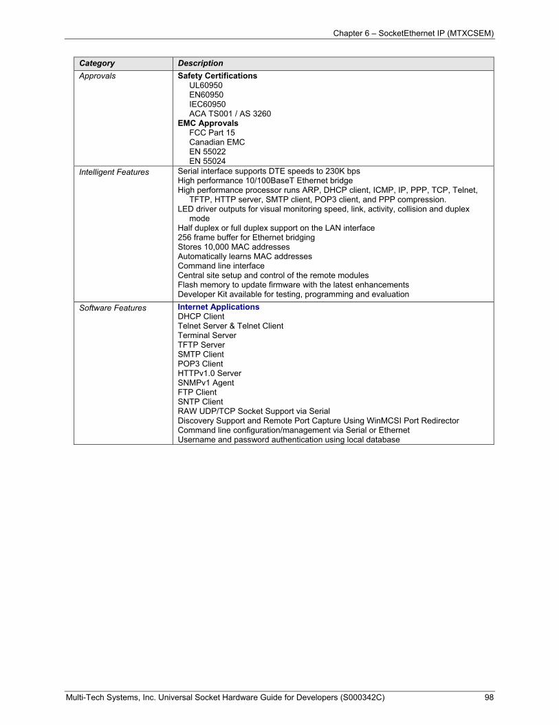
Chapter 6 – SocketEthernet IP (MTXCSEM)
Multi-Tech Systems, Inc. Universal Socket Hardware Guide for Developers (S000342C) 98
Category Description Approvals Safety Certifications
UL60950 EN60950 IEC60950 ACA TS001 / AS 3260
EMC Approvals FCC Part 15 Canadian EMC EN 55022 EN 55024
Intelligent Features Serial interface supports DTE speeds to 230K bps High performance 10/100BaseT Ethernet bridge High performance processor runs ARP, DHCP client, ICMP, IP, PPP, TCP, Telnet,
TFTP, HTTP server, SMTP client, POP3 client, and PPP compression. LED driver outputs for visual monitoring speed, link, activity, collision and duplex
mode Half duplex or full duplex support on the LAN interface 256 frame buffer for Ethernet bridging Stores 10,000 MAC addresses Automatically learns MAC addresses Command line interface Central site setup and control of the remote modules Flash memory to update firmware with the latest enhancements Developer Kit available for testing, programming and evaluation
Software Features Internet Applications DHCP Client Telnet Server & Telnet Client Terminal Server TFTP Server SMTP Client POP3 Client HTTPv1.0 Server SNMPv1 Agent FTP Client SNTP Client RAW UDP/TCP Socket Support via Serial Discovery Support and Remote Port Capture Using WinMCSI Port Redirector Command line configuration/management via Serial or Ethernet Username and password authentication using local database
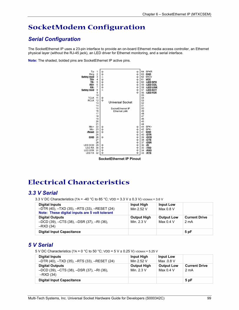
Chapter 6 – SocketEthernet IP (MTXCSEM)
Multi-Tech Systems, Inc. Universal Socket Hardware Guide for Developers (S000342C) 99
SocketModem Configuration
Serial Configuration The SocketEthernet IP uses a 23-pin interface to provide an on-board Ethernet media access controller, an Ethernet physical layer (without the RJ-45 jack), an LED driver for Ethernet monitoring, and a serial interface.
Note: The shaded, bolded pins are SocketEthernet IP active pins.
SocketEthernet IP Pinout
Electrical Characteristics
3.3 V Serial 3.3 V DC Characteristics (TA = -40 °C to 85 °C; VDD = 3.3 V ± 0.3 V) VDDMAX = 3.6 V
Digital Inputs –DTR (40), –TXD (35), –RTS (33), –RESET (24) Note: These digital inputs are 5 volt tolerant
Input High Min 2.52 V
Input Low Max 0.8 V
Digital Outputs –DCD (39), –CTS (38), –DSR (37), –RI (36), –RXD (34)
Output High Min. 2.3 V
Output Low Max 0.4 V
Current Drive 2 mA
Digital Input Capacitance 5 pF
5 V Serial 5 V DC Characteristics (TA = 0 °C to 50 °C; VDD = 5 V ± 0.25 V) VDDMAX = 5.25 V
Digital Inputs –DTR (40), –TXD (35), –RTS (33), –RESET (24)
Input High Min 2.52 V
Input Low Max .0.8 V
Digital Outputs –DCD (39), –CTS (38), –DSR (37), –RI (36), –RXD (34)
Output High Min. 2.3 V
Output Low Max 0.4 V
Current Drive 2 mA
Digital Input Capacitance 5 pF
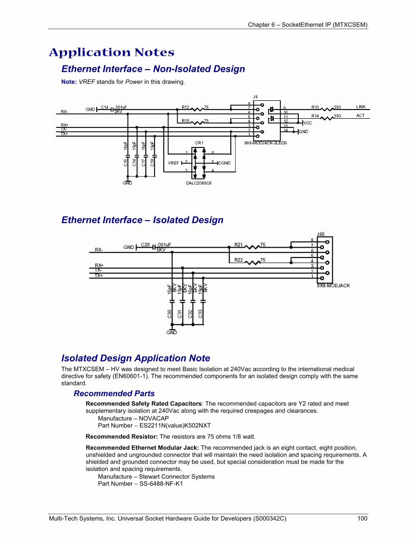
Chapter 6 – SocketEthernet IP (MTXCSEM)
Multi-Tech Systems, Inc. Universal Socket Hardware Guide for Developers (S000342C) 100
Application Notes
Ethernet Interface – Non-Isolated Design Note: VREF stands for Power in this drawing.
Ethernet Interface – Isolated Design
Isolated Design Application Note The MTXCSEM – HV was designed to meet Basic Isolation at 240Vac according to the international medical directive for safety (EN60601-1). The recommended components for an isolated design comply with the same standard.
Recommended Parts Recommended Safety Rated Capacitors: The recommended capacitors are Y2 rated and meet supplementary isolation at 240Vac along with the required creepages and clearances.
Manufacture – NOVACAP Part Number – ES2211N(value)K502NXT
Recommended Resistor: The resistors are 75 ohms 1/8 watt.
Recommended Ethernet Modular Jack: The recommended jack is an eight contact, eight position, unshielded and ungrounded connector that will maintain the need isolation and spacing requirements. A shielded and grounded connector may be used, but special consideration must be made for the isolation and spacing requirements.
Manufacture – Stewart Connector Systems Part Number – SS-6488-NF-K1
Multi-Tech Systems, Inc. Universal Socket Hardware Guide for Developers (S000342C) 101
Chapter 7
SocketModem ISDN
MT128SMI
Chapter 7 – SocketModem ISDN (MT128SMI)
Multi-Tech Systems, Inc. Universal Socket Hardware Guide for Developers (S000342C) 102
Chapter 7 – SocketModem ISDN (MT128SMI)
Introduction The Multi-Tech SocketModem ISDN creates communication-ready devices by integrating BRI ISDN functionality and S/T interface into a single, universal socket design. The space-efficient (1” x 2.5”) embedded modem provides bi-directional communication bandwidth of up to 128K bps. This complete, ready-to-integrate modem dramatically reduces development time and costs for system designers.
Product Ordering Information Product Description Region Order this
Product
MT128SMI 64/128K ISDN BRI S/T Interface – 5 V Euro/ROW MT128SMI-L 64/128K ISDN BRI S/T Interface – 3.3 V Euro/ROW
Developer Kit MTSMI-IDK SocketModem ISDN Developer Kit 100-240 V Global
Developer Kit The SocketModem ISDN Developer Kit provides the ability to plug in the ISDN module and use it for testing, programming and evaluation. The kit includes one developer board with RS-232 DB-25 connector, wall power adapter, RJ-45 jack, RS-232 cable, and Developer Guide CD.
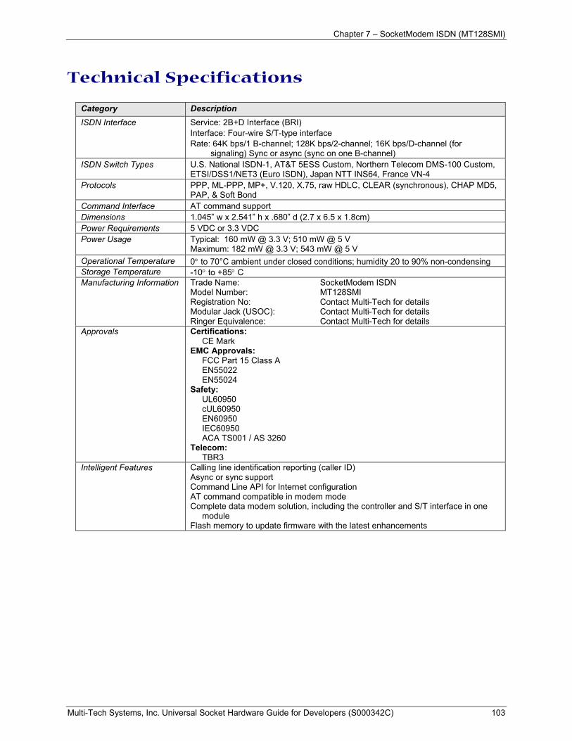
Chapter 7 – SocketModem ISDN (MT128SMI)
Multi-Tech Systems, Inc. Universal Socket Hardware Guide for Developers (S000342C) 103
Technical Specifications
Category Description ISDN Interface Service: 2B+D Interface (BRI)
Interface: Four-wire S/T-type interface Rate: 64K bps/1 B-channel; 128K bps/2-channel; 16K bps/D-channel (for
signaling) Sync or async (sync on one B-channel) ISDN Switch Types U.S. National ISDN-1, AT&T 5ESS Custom, Northern Telecom DMS-100 Custom,
ETSI/DSS1/NET3 (Euro ISDN), Japan NTT INS64, France VN-4 Protocols PPP, ML-PPP, MP+, V.120, X.75, raw HDLC, CLEAR (synchronous), CHAP MD5,
PAP, & Soft Bond Command Interface AT command support Dimensions 1.045” w x 2.541” h x .680” d (2.7 x 6.5 x 1.8cm) Power Requirements 5 VDC or 3.3 VDC Power Usage
Typical: 160 mW @ 3.3 V; 510 mW @ 5 V Maximum: 182 mW @ 3.3 V; 543 mW @ 5 V
Operational Temperature 0° to 70°C ambient under closed conditions; humidity 20 to 90% non-condensing Storage Temperature -10° to +85° C Manufacturing Information Trade Name: SocketModem ISDN
Model Number: MT128SMI Registration No: Contact Multi-Tech for details Modular Jack (USOC): Contact Multi-Tech for details Ringer Equivalence: Contact Multi-Tech for details
Approvals Certifications: CE Mark
EMC Approvals: FCC Part 15 Class A EN55022 EN55024
Safety: UL60950 cUL60950 EN60950 IEC60950 ACA TS001 / AS 3260 Telecom:
TBR3 Intelligent Features Calling line identification reporting (caller ID)
Async or sync support Command Line API for Internet configuration AT command compatible in modem mode Complete data modem solution, including the controller and S/T interface in one
module Flash memory to update firmware with the latest enhancements
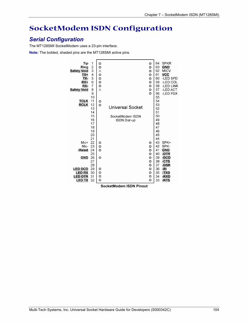
Chapter 7 – SocketModem ISDN (MT128SMI)
Multi-Tech Systems, Inc. Universal Socket Hardware Guide for Developers (S000342C) 104
SocketModem ISDN Configuration
Serial Configuration The MT128SMI SocketModem uses a 23-pin interface.
Note: The bolded, shaded pins are the MT128SMI active pins.
SocketModem ISDN Pinout
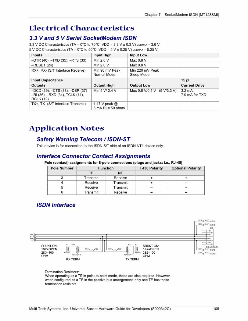
Chapter 7 – SocketModem ISDN (MT128SMI)
Multi-Tech Systems, Inc. Universal Socket Hardware Guide for Developers (S000342C) 105
Electrical Characteristics
3.3 V and 5 V Serial SocketModem ISDN 3.3 V DC Characteristics (TA = 0°C to 70°C; VDD = 3.3 V ± 0.3 V) VDDMAX = 3.6 V 5 V DC Characteristics (TA = 0°C to 50°C; VDD = 5 V ± 0.25 V) VDDMAX = 5.25 V
Inputs Input High Input Low –DTR (40), –TXD (35), –RTS (33) Min 2.0 V Max 0.8 V –RESET (24) Min 2.0 V Max 0.8 V RX+, RX- (S/T Interface Receive)
Min 90 mV Peak Normal Mode
Min 220 mV Peak Sleep Mode
Input Capacitance 15 pF Outputs Output High Output Low Current Drive –DCD (39), –CTS (38), –DSR (37) –RI (36), –RXD (34), TCLK (11), RCLK (12)
Min 4 V/ 2.4 V Max 0.5 V/0.5 V (5 V/3.3 V) 3.2 mA, 7.0 mA for TXD
TX+, TX- (S/T Interface Transmit) 1.17 V peak @ 6 mA RL= 50 ohms
Application Notes
Safety Warning Telecom / ISDN-ST This device is for connection to the ISDN S/T side of an ISDN NT1 device only.
Interface Connector Contact Assignments Pole (contact) assignments for 8-pole connections (plugs and jacks; i.e., RJ-45)
Function I.430 Polarity Optional Polarity Pole Number TE NT
3 Transmit Receive + + 4 Receive Transmit + – 5 Receive Transmit – + 6 Transmit Receive – –
ISDN Interface
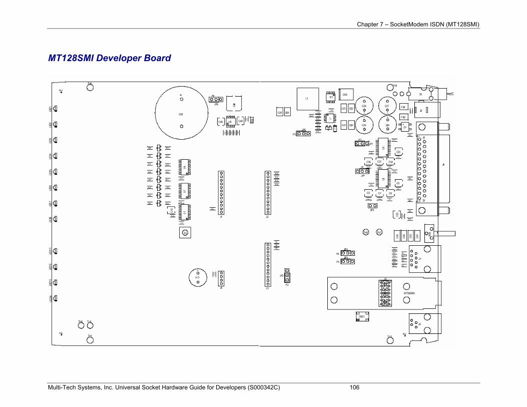
Chapter 7 – SocketModem ISDN (MT128SMI)
Multi-Tech Systems, Inc. Universal Socket Hardware Guide for Developers (S000342C) 106
MT128SMI Developer Board
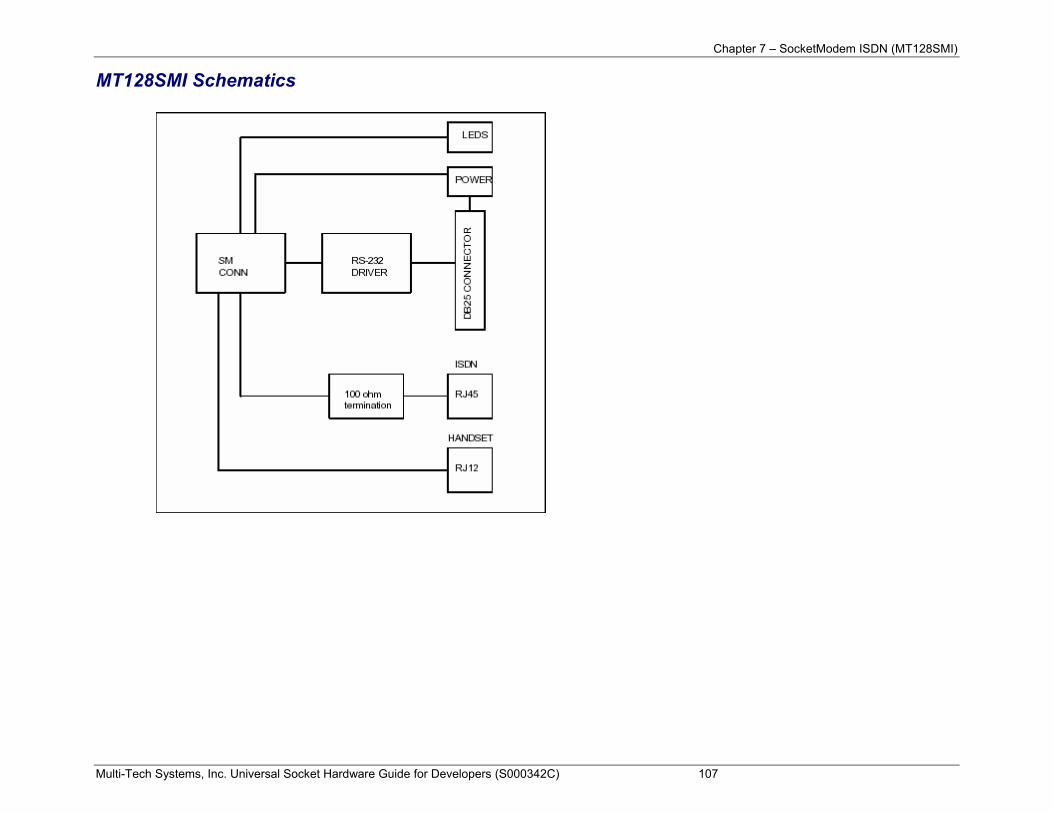
Chapter 7 – SocketModem ISDN (MT128SMI)
Multi-Tech Systems, Inc. Universal Socket Hardware Guide for Developers (S000342C) 107
MT128SMI Schematics
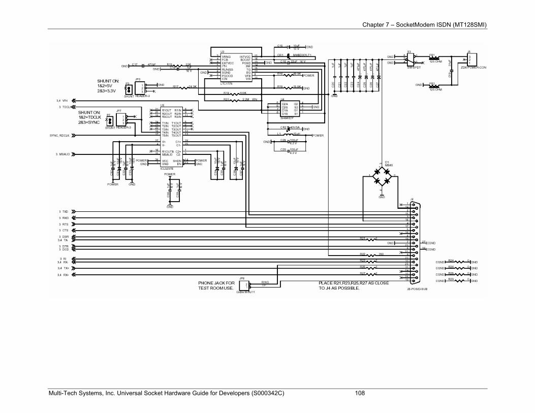
Chapter 7 – SocketModem ISDN (MT128SMI)
Multi-Tech Systems, Inc. Universal Socket Hardware Guide for Developers (S000342C) 108
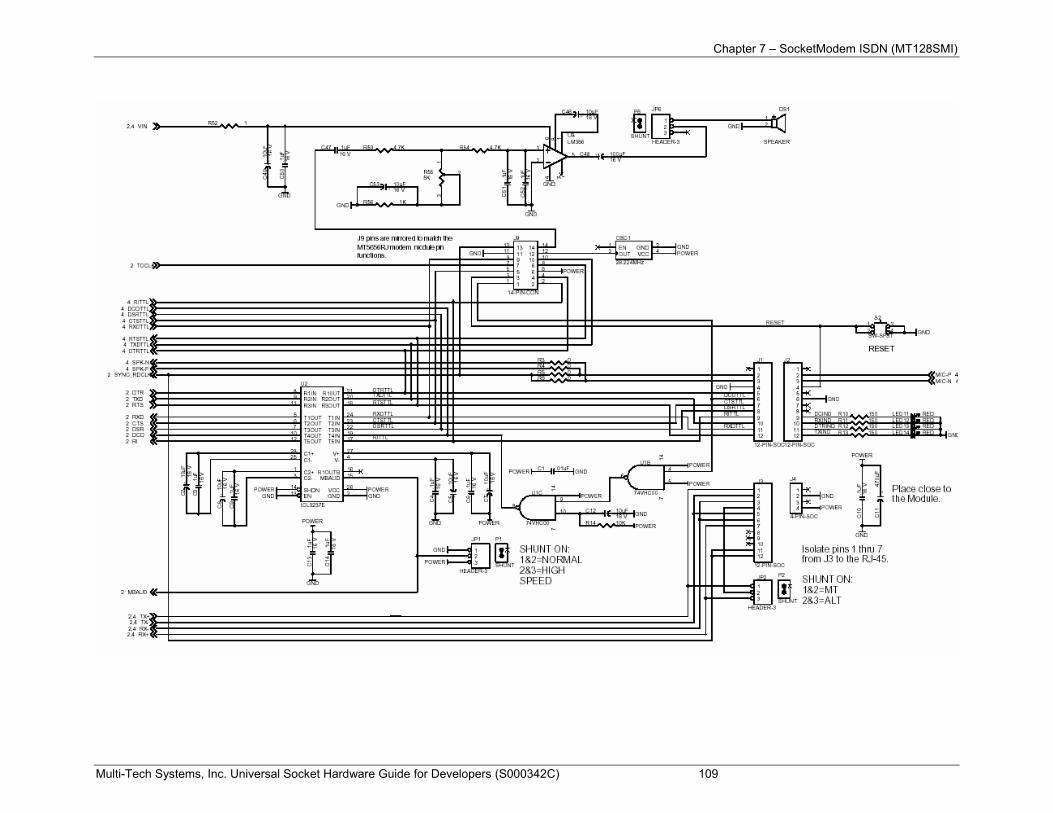
Chapter 7 – SocketModem ISDN (MT128SMI)
Multi-Tech Systems, Inc. Universal Socket Hardware Guide for Developers (S000342C) 109
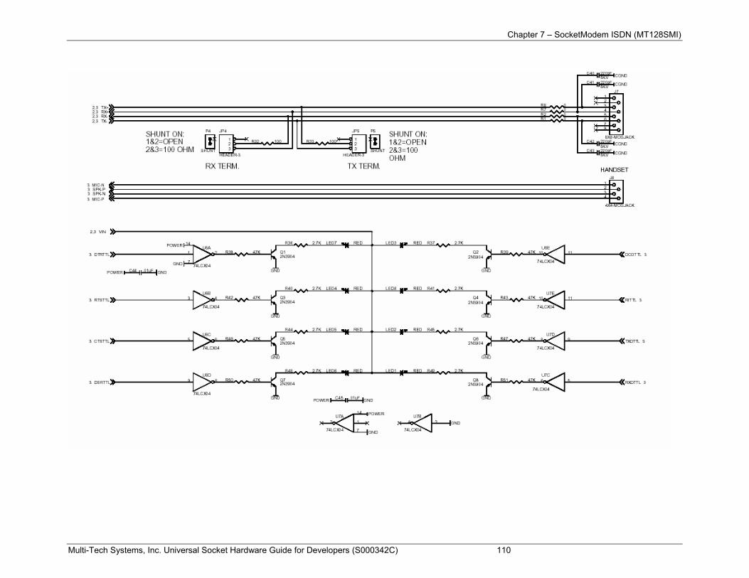
Chapter 7 – SocketModem ISDN (MT128SMI)
Multi-Tech Systems, Inc. Universal Socket Hardware Guide for Developers (S000342C) 110
Multi-Tech Systems, Inc. Universal Socket Hardware Guide for Developers (S000342C) 111
Chapter 8
SocketModem GPRS
MTSMC-G
Chapter 8 – SocketModem GPRS (MTSMC-G)
Multi-Tech Systems, Inc. Universal Socket Hardware Guide for Developers (S000342C) 112
Chapter 8 – SocketModem GPRS (MTSMC-G)
Product Description The Multi-Tech SocketModem GPRS is a complete, ready-to-integrate, embedded wireless modem. Designed for global use, it offers standards-based multi-band GSM/GPRS Class 10. The SocketModem GSM/GPRS is based on industry-standard open interfaces and utilizes the same form factor as the SocketModem, SocketModem IP, or SocketEthernet IP modules from Multi-Tech.
Notes about Activation: • These units are shipped without network activation. • To connect to the wireless network, you will have to establish a wireless account. Call Multi-Tech Systems,
Inc. to set up your account: 888-288-5470
• See the Wireless Activation procedures in a separate document available on the Developer Kit CD.
Product Ordering Information
Product Description Region Order this Product
MTSMC-G-F1 900/1800 MHz GSM/GPRS SocketModem – 5 V Europe/Asia/Africa MTSMC-G-F2 850/1900 MHz GSM/GPRS SocketModem – 5 V North/South America
Antennas and Cables 45009650 Dual-band antenna for F2-type and CDMA modems
(Green Dot) ¼ Wave, Stubby Global
45009660 Dual-band antenna for F1-type modems (Orange Dot) ¼ Wave, Stubby
Global
45009670 Dual-band antenna for the F2-type and CDMA modems ½ Wave, Right Angle
Global
45009675 Dual-band antenna for the F1-type modems ½ Wave, Right Angle
Global
45009630 SMA to MMCX COAX RF cable (6 inches) Global Developer Kit
MTSMC-DK SocketModem GPRS Developer Kit Global
Developer Kit The SocketModem GPRS Developer Kit allows you to plug in the SocketModem and use it for testing, programming, and evaluation. The kit includes:
• one developer board with RS-232 DB-25 connector • universal power supply • antenna • RS-232 cable • Developer Kit CD
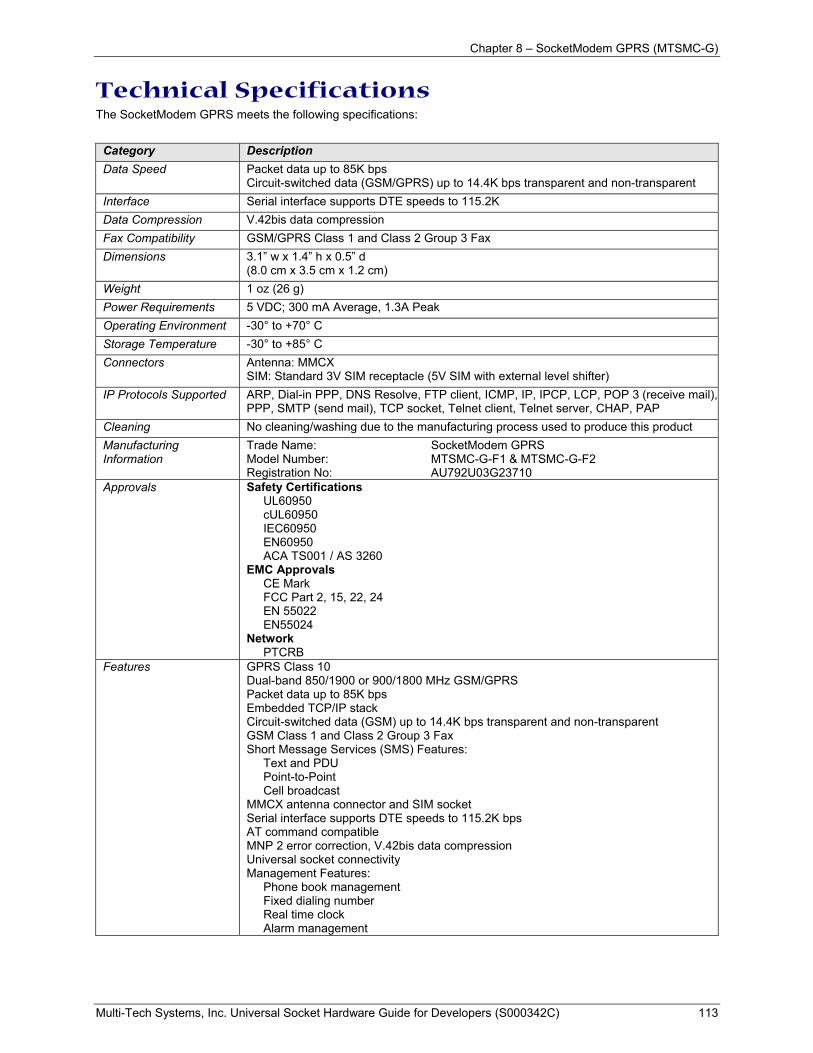
Chapter 8 – SocketModem GPRS (MTSMC-G)
Multi-Tech Systems, Inc. Universal Socket Hardware Guide for Developers (S000342C) 113
Technical Specifications The SocketModem GPRS meets the following specifications:
Category Description Data Speed Packet data up to 85K bps
Circuit-switched data (GSM/GPRS) up to 14.4K bps transparent and non-transparent Interface Serial interface supports DTE speeds to 115.2K Data Compression V.42bis data compression Fax Compatibility GSM/GPRS Class 1 and Class 2 Group 3 Fax Dimensions 3.1” w x 1.4” h x 0.5” d
(8.0 cm x 3.5 cm x 1.2 cm) Weight 1 oz (26 g) Power Requirements 5 VDC; 300 mA Average, 1.3A Peak Operating Environment -30° to +70° C Storage Temperature -30° to +85° C Connectors Antenna: MMCX
SIM: Standard 3V SIM receptacle (5V SIM with external level shifter) IP Protocols Supported ARP, Dial-in PPP, DNS Resolve, FTP client, ICMP, IP, IPCP, LCP, POP 3 (receive mail),
PPP, SMTP (send mail), TCP socket, Telnet client, Telnet server, CHAP, PAP Cleaning No cleaning/washing due to the manufacturing process used to produce this product Manufacturing Information
Trade Name: SocketModem GPRS Model Number: MTSMC-G-F1 & MTSMC-G-F2 Registration No: AU792U03G23710
Approvals Safety Certifications UL60950 cUL60950 IEC60950 EN60950 ACA TS001 / AS 3260
EMC Approvals CE Mark FCC Part 2, 15, 22, 24 EN 55022 EN55024
Network PTCRB
Features GPRS Class 10 Dual-band 850/1900 or 900/1800 MHz GSM/GPRS Packet data up to 85K bps Embedded TCP/IP stack Circuit-switched data (GSM) up to 14.4K bps transparent and non-transparent GSM Class 1 and Class 2 Group 3 Fax Short Message Services (SMS) Features:
Text and PDU Point-to-Point Cell broadcast
MMCX antenna connector and SIM socket Serial interface supports DTE speeds to 115.2K bps AT command compatible MNP 2 error correction, V.42bis data compression Universal socket connectivity Management Features:
Phone book management Fixed dialing number Real time clock Alarm management
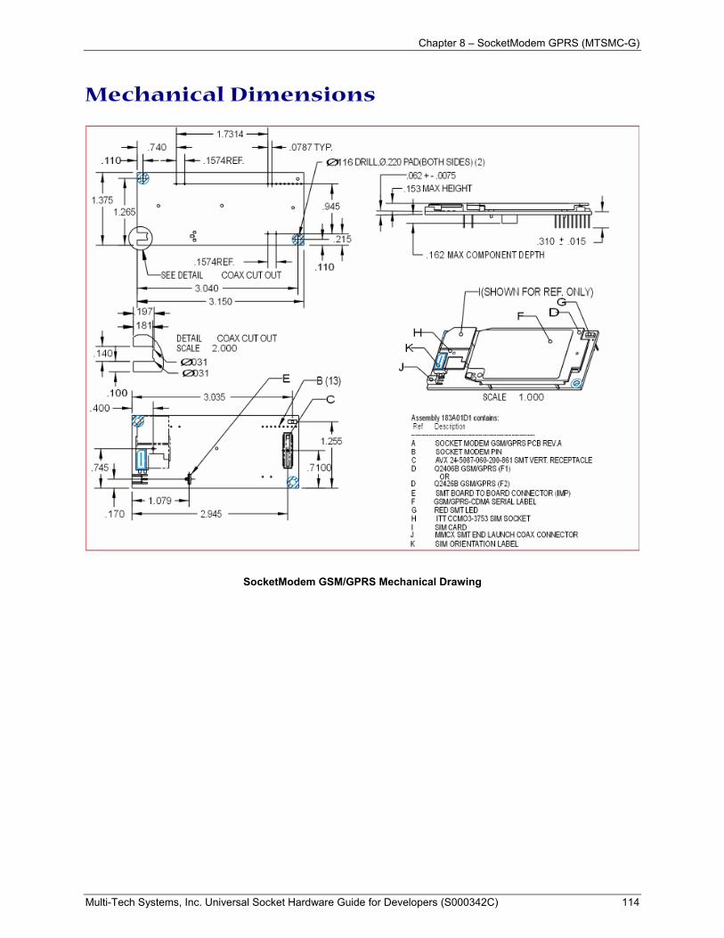
Chapter 8 – SocketModem GPRS (MTSMC-G)
Multi-Tech Systems, Inc. Universal Socket Hardware Guide for Developers (S000342C) 114
Mechanical Dimensions
SocketModem GSM/GPRS Mechanical Drawing
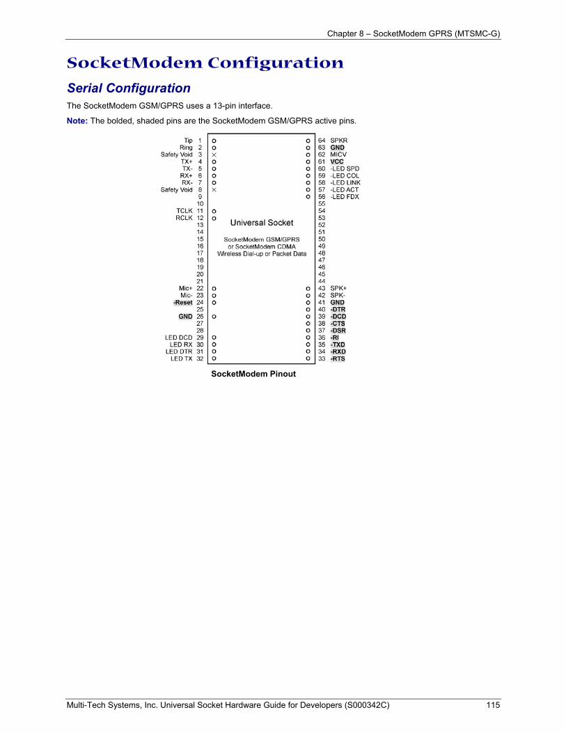
Chapter 8 – SocketModem GPRS (MTSMC-G)
Multi-Tech Systems, Inc. Universal Socket Hardware Guide for Developers (S000342C) 115
SocketModem Configuration
Serial Configuration The SocketModem GSM/GPRS uses a 13-pin interface.
Note: The bolded, shaded pins are the SocketModem GSM/GPRS active pins.
SocketModem Pinout
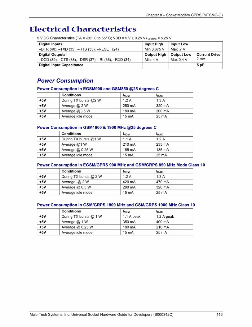
Chapter 8 – SocketModem GPRS (MTSMC-G)
Multi-Tech Systems, Inc. Universal Socket Hardware Guide for Developers (S000342C) 116
Electrical Characteristics 5 V DC Characteristics (TA = -20° C to 55° C; VDD = 5 V ± 0.25 V) VDDMAX = 5.25 V Digital Inputs –DTR (40), –TXD (35), –RTS (33), –RESET (24)
Input High Min 3.675 V
Input Low Max .7 V
Digital Outputs –DCD (39), –CTS (38), –DSR (37), –RI (36), –RXD (34)
Output High Min. 4 V
Output Low Max 0.4 V
Current Drive: 2 mA
Digital Input Capacitance 5 pF
Power Consumption Power Consumption in EGSM900 and GSM850 @25 degrees C
Conditions INOM IMAX +5V During TX bursts @2 W 1.2 A 1.3 A +5V Average @ 2 W 250 mA 320 mA +5V Average @ ).5 W 180 mA 200 mA +5V Average idle mode 15 mA 25 mA
Power Consumption in GSM1800 & 1900 MHz @25 degrees C
Conditions INOM IMAX +5V During TX bursts @1 W 1.1 A 1.2 A +5V Average @1 W 210 mA 235 mA +5V Average @ 0.25 W 165 mA 185 mA +5V Average idle mode 15 mA 25 mA
Power Consumption in EGSM/GPRS 900 MHz and GSM/GRPS 850 MHz Mode Class 10
Conditions INOM IMAX +5V During TX bursts @ 2 W 1.2 A 1.3 A +5V Average @ 2 W 420 mA 470 mA +5V Average @ 0.5 W 280 mA 320 mA +5V Average idle mode 15 mA 25 mA
Power Consumption in GSM/GRPS 1800 MHz and GSM/GRPS 1900 MHz Class 10 Conditions INOM IMAX +5V During TX bursts @ 1 W 1.1 A peak 1.2 A peak +5V Average @ 1 W 350 mA 400 mA +5V Average @ 0.25 W 180 mA 210 mA +5V Average idle mode 15 mA 25 mA
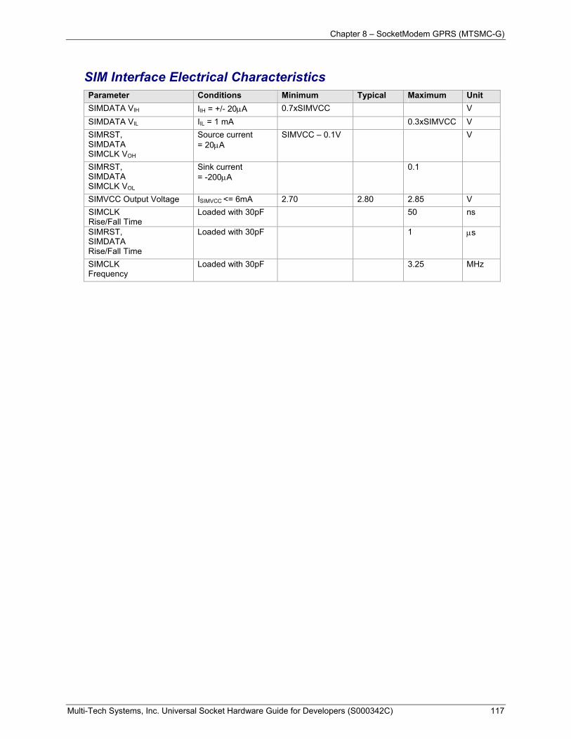
Chapter 8 – SocketModem GPRS (MTSMC-G)
Multi-Tech Systems, Inc. Universal Socket Hardware Guide for Developers (S000342C) 117
SIM Interface Electrical Characteristics Parameter Conditions Minimum Typical Maximum Unit SIMDATA VIH IIH = +/- 20µA 0.7xSIMVCC V SIMDATA VIL IIL = 1 mA 0.3xSIMVCC V SIMRST, SIMDATA SIMCLK VOH
Source current = 20µA
SIMVCC – 0.1V V
SIMRST, SIMDATA SIMCLK VOL
Sink current = -200µA
0.1
SIMVCC Output Voltage ISIMVCC <= 6mA 2.70 2.80 2.85 V SIMCLK Rise/Fall Time
Loaded with 30pF 50 ns
SIMRST, SIMDATA Rise/Fall Time
Loaded with 30pF 1 µs
SIMCLK Frequency
Loaded with 30pF 3.25 MHz
Chapter 8 – SocketModem GPRS (MTSMC-G)
Multi-Tech Systems, Inc. Universal Socket Hardware Guide for Developers (S000342C) 118
Application Notes SocketModem GSM/GPRS Interfaces • Flashing LED • SIM Interface • RF Interface
Flashing LED Interface The flashing LED signal is used to indicate the working mode of the SocketModem.
LED and SocketModem Status Signal SocketModem Status OFF Download mode or switched OFF>
Continuously lit Switched ON (not registered on the network) ON Flashing Switched ON (registered on the network)
SIM Interface The internal SIM interface of the SocketModem supports 3V SIMs only. Note: This interface is fully compliant with GSM 11.11 recommendations concerning the SIM functionality. Five Signals Are Available SIMVCC: SIM power supply. SIMRST: reset. SIMCLK: clock. SIMDATA: I/O port. SIMPRES1 SIM card detect.
RF Interface The impedance is 50 Ohms nominal.
RF Connector The RF connector is MMCX standard type. An antenna can be directly connected through the mating connector or using a small adapter.
RF Performances RF performances are compliant with the ETSI recommendation 05.05 and 11.10. The main parameters are:
Receiver Features • EGSM Sensitivity : < -104 dBm • GSM 1800/GSM 1900 Sensitivity : < -102 dBm • Selectivity @ 200 kHz : > +9 dBc • Selectivity @ 400 kHz : > +41 dBc • Dynamic range : 62 dB • Intermodulation : > -43 dBm • Co-channel rejection : + 9 dBc
Transmitter Features • Maximum output power (EGSM) : 33 dBm ± 2 dB • Maximum output power (DCS/PCS) : 30 dBm ± 2 dB • Minimum output power (EGSM): 5 dBm ± 5 dB • Minimum output power (DCS/PCS): 0 dBm ± 5 dB • H2 level : < -30 dBm • H3 level : < -30 dBm • Noise in 925 - 935 MHz : < -67 dBm • Noise in 935 - 960 MHz : < -79 dBm • Noise in 1805 - 1880 MHz : < -71 dBm • Phase error at peak power : < 5 ° RMS • Frequency error : ± 0.1 ppm max
Chapter 8 – SocketModem GPRS (MTSMC-G)
Multi-Tech Systems, Inc. Universal Socket Hardware Guide for Developers (S000342C) 119
General Guidelines for the Use of the SocketModem Hardware and RF
• Ground plane: Multi-Tech recommends having a common ground plane for analog, digital, and RF grounds.
• ESD protection on serial link. • Possible spurious emission radiated by the application to the RF receiver in the receiver band
The Antenna The antenna sub-system and integration in the application is a major issue: Choice of antenna cable (type, length, performances, thermal resistance, etc.) These elements could affect GSM performances such as sensitivity and emitted power. The antenna should be isolated as much as possible from the digital circuitry including the interface signals. Multi-Tech recommends shielding the terminal. On terminals including the antenna, a poor shielding could dramatically affect the sensitivity of the terminal. Subsequently, the power emitted through the antenna could affect the application.
Soldering and Cleaning the SocketModem The pins of the SocketModem may be hand soldered or wave soldered. If wave soldered, the temperature on the top of the SocketModem must not exceed 100° C. There should be no solvent or water washing of the SocketModem. Do not use a hot air gun on the SocketModem.
Initial Configuration Using Mobile PhoneTools For initial configuration of your wireless device, Multi-Tech offers a Windows-based mobile PhoneTools application. To load Mobile PhoneTools, click the Mobile PhoneTools icon on the SocketModem CD and follow the on-screen prompts.
Sources for Peripheral Devices GSM Antenna
The integrated modem antenna connector is a MMCX connector. The MMCX connector incorporates a 'Snap On' latching action in order to make the connection easier with an excellent RF performance. An additional advantage is its small physical size, which is 50% of the standard MCX connector. This type of connector is suitable for the standard ranges of flexible and semi-rigid cables. The characteristic impedance of the MMCX coaxial connector is 50 ohm. The antenna manufacturer must guarantee that the antenna will be working according to the radio characteristics presented in the table below.
Radio Characteristics GSM 850 EGSM 900 GSM 1800 GSM 1900
Frequency RX 869 to 894 MHz 925 to 960 MHz 1805 to 1880 MHz 1930 to 1990 MHz Frequency TX 824 to 849 MHz 880 to 915 MHz 1710 to 1785 MHz 1850 to 1910 MHz RF Power Stand 2W at 12.5% duty cycle 2W at 12.5% duty cycle 1W at 12.5% duty cycle 1W at 12.5% duty cycle
Impedance 50 ohms VSWR <2 Typical Radiated Gain 0 dBi on azimuth plane
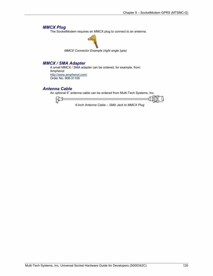
Chapter 8 – SocketModem GPRS (MTSMC-G)
Multi-Tech Systems, Inc. Universal Socket Hardware Guide for Developers (S000342C) 120
MMCX Plug The SocketModem requires an MMCX plug to connect to an antenna.
MMCX Connector Example (right angle type)
MMCX / SMA Adapter A small MMCX / SMA adapter can be ordered, for example, from: Amphenol http://www.amphenol.com/ Order No: 908-31100
Antenna Cable An optional 6” antenna cable can be ordered from Multi-Tech Systems, Inc.
6-Inch Antenna Cable – SMA Jack to MMCX Plug
Multi-Tech Systems, Inc. Universal Socket Hardware Guide for Developers (S000342C) 121
Chapter 9
SocketModem CDMA
MTSMC-C
Chapter 9 – SocketModem CDMA (MTSMC-C)
Multi-Tech Systems, Inc. Universal Socket Hardware Guide for Developers (S000342C) 122
Chapter 9 – SocketModem CDMA (MTSMC-C)
The Multi-Tech SocketModem CDMA is a complete, ready-to-integrate, embedded wireless modem. Designed for global use, it offers standards-based multi-band CDMA200 1x performance. The SocketModem CDMA is based on industry-standard open interfaces and utilizes Multi-Tech’s universal socket design.
Notes about Activation: • These units are shipped without network activation. • To connect to the wireless network, you will have to establish a wireless account. Call Multi-Tech Systems,
Inc. to set up your account: 888-288-5470.
• See the Wireless Activation procedures in a separate document available on the Developer Kit CD.
Product Ordering Information
Product Description Region Order this Product
MTSMC-C-N1 800/1900 CDMA 1xRTT Generic SocketModem – 5 V Global MTSMC-C-N2 800/1900 CDMA 1xRTT Sprint SocketModem – 5 V Global MTSMC-C-N3 800/1900 CDMA 1xRTT Verizon SocketModem – 5 V Global
Antennas and Cables 45009650 Dual-band antenna for CDMA and F2 type modems
(Green Dot) Global
45009630 SMA to MMCX COAX RF cable (6 inches) Global 45009670 Dual-band antenna for the F2-type and CDMA modems
½ Wave, Right Angle Global
Developer Kit MTSMC-DK SocketModem Wireless Developer Kit Global
Developer Kit The SocketModem CDMA Developer Kit allows you to plug in the SocketModem and use it for testing, programming, and evaluation. The kit includes:
• one developer board with RS-232 DB-25 connector • universal power supply • antenna • RS-232 cable • Developer Kit CD
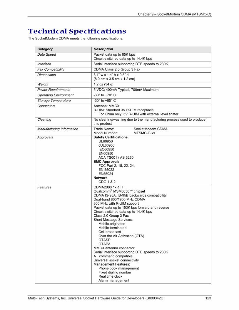
Chapter 9 – SocketModem CDMA (MTSMC-C)
Multi-Tech Systems, Inc. Universal Socket Hardware Guide for Developers (S000342C) 123
Technical Specifications The SocketModem CDMA meets the following specifications:
Category Description Data Speed Packet data up to 85K bps
Circuit-switched data up to 14.4K bps Interface Serial interface supporting DTE speeds to 230K Fax Compatibility CDMA Class 2.0 Group 3 Fax Dimensions 3.1” w x 1.4” h x 0.5” d
(8.0 cm x 3.5 cm x 1.2 cm) Weight 1.2 oz (34 g) Power Requirements 5 VDC; 400mA Typical, 700mA Maximum Operating Environment -30° to +70° C Storage Temperature -30° to +85° C Connectors Antenna: MMCX
R-UIM: Standard 3V R-UIM receptacle For China only, 5V R-UIM with external level shifter
Cleaning No cleaning/washing due to the manufacturing process used to produce this product
Manufacturing Information Trade Name: SocketModem CDMA Model Number: MTSMC-C-xx
Approvals Safety Certifications UL60950 cUL60950 IEC60950 EN60950 ACA TS001 / AS 3260
EMC Approvals FCC Part 2, 15, 22, 24, EN 55022 EN55024
Network CDG 1 & 2
Features CDMA2000 1xRTT Qualcomm® MSM6050™ chipset CDMA IS-95A, IS-95B backwards compatibility Dual-band 800/1900 MHz CDMA 800 MHz with R-UIM support Packet data up to 153K bps forward and reverse Circuit-switched data up to 14.4K bps Class 2.0 Group 3 Fax Short Message Services:
Mobile originated Mobile terminated Cell broadcast Over the Air Activation (OTA) OTASP OTAPA
MMCX antenna connector Serial interface supporting DTE speeds to 230K AT command compatible Universal socket connectivity Management Features:
Phone book management Fixed dialing number Real time clock Alarm management
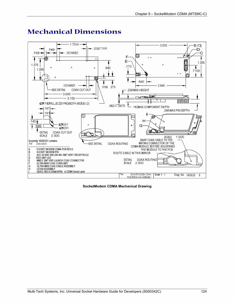
Chapter 9 – SocketModem CDMA (MTSMC-C)
Multi-Tech Systems, Inc. Universal Socket Hardware Guide for Developers (S000342C) 124
Mechanical Dimensions
SocketModem CDMA Mechanical Drawing
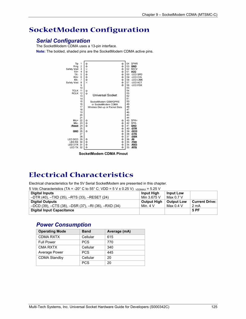
Chapter 9 – SocketModem CDMA (MTSMC-C)
Multi-Tech Systems, Inc. Universal Socket Hardware Guide for Developers (S000342C) 125
SocketModem Configuration
Serial Configuration The SocketModem CDMA uses a 13-pin interface. Note: The bolded, shaded pins are the SocketModem CDMA active pins.
SocketModem CDMA Pinout
Electrical Characteristics Electrical characteristics for the 5V Serial SocketModem are presented in this chapter. 5 Vdc Characteristics (TA = -20° C to 55° C; VDD = 5 V ± 0.25 V) VDDMAX = 5.25 V Digital Inputs –DTR (40), –TXD (35), –RTS (33), –RESET (24)
Input High Min 3.675 V
Input Low Max 0.7 V
Digital Outputs –DCD (39), –CTS (38), –DSR (37), –RI (36), –RXD (34)
Output High Min. 4 V
Output Low Max 0.4 V
Current Drive: 2 mA
Digital Input Capacitance 5 PF
Power Consumption Operating Mode Band Average (mA) CDMA RXTX Cellular 615 Full Power PCS 770
Cellular 340 CMA RXTX Average Power PCS 445
Cellular 20 CDMA Standby PCS 20
Chapter 9 – SocketModem CDMA (MTSMC-C)
Multi-Tech Systems, Inc. Universal Socket Hardware Guide for Developers (S000342C) 126
Application Notes
SocketModem Interfaces
Flashing LED Interface The flashing LED signal is used to indicate the working mode of the SocketModem. LED and SocketModem Status
Signal SocketModem Status OFF Download mode or switched OFF>
Continuously lit Switched ON (not registered on the network) ON Flashing Switched ON (registered on the network)
RF Interface The impedance is 50 Ohms nominal.
RF Connector The RF connector is MMCX standard type. An antenna can be directly connected through the mating connector or using a small adapter.
General Guidelines for the Use of the SocketModem Hardware and RF
• Ground plane: Multi-Tech recommends having a common ground plane for analog, digital, and RF grounds.
• ESD protection on serial link, • Possible spurious emission radiated by the application to the RF receiver in the receiver band.
The Antenna The antenna sub-system and integration in the application is a major issue: Choice of antenna cable (type, length, performances, thermal resistance, etc.) These elements could affect CDMA performances such as sensitivity and emitted power. The antenna should be isolated as much as possible from the digital circuitry including the interface signals. Multi-Tech recommends shielding the terminal. On terminals including the antenna, a poor shielding could dramatically affect the sensitivity of the terminal. Subsequently, the power emitted through the antenna could affect the application.
Soldering and Cleaning the SocketModem The pins of the SocketModem may be hand soldered or wave soldered. If wave soldered, the temperature on the top of the SocketModem must not exceed 100° C. There should be no solvent or water washing of the SocketModem. Do not use a hot air gun on the SocketModem.
Initial Configuration Using Mobile PhoneTools For initial configuration of your wireless device, Multi-Tech offers a Windows-based mobile PhoneTools application. To load Mobile PhoneTools: Click the Mobile PhoneTools icon on the product CD and follow the on-screen prompts.
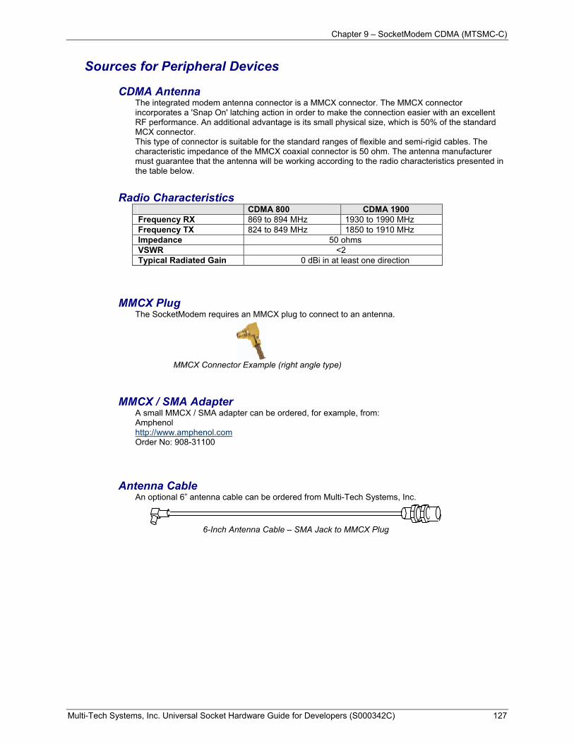
Chapter 9 – SocketModem CDMA (MTSMC-C)
Multi-Tech Systems, Inc. Universal Socket Hardware Guide for Developers (S000342C) 127
Sources for Peripheral Devices
CDMA Antenna The integrated modem antenna connector is a MMCX connector. The MMCX connector incorporates a 'Snap On' latching action in order to make the connection easier with an excellent RF performance. An additional advantage is its small physical size, which is 50% of the standard MCX connector. This type of connector is suitable for the standard ranges of flexible and semi-rigid cables. The characteristic impedance of the MMCX coaxial connector is 50 ohm. The antenna manufacturer must guarantee that the antenna will be working according to the radio characteristics presented in the table below.
Radio Characteristics CDMA 800 CDMA 1900 Frequency RX 869 to 894 MHz 1930 to 1990 MHz Frequency TX 824 to 849 MHz 1850 to 1910 MHz Impedance 50 ohms VSWR <2 Typical Radiated Gain 0 dBi in at least one direction
MMCX Plug The SocketModem requires an MMCX plug to connect to an antenna.
MMCX Connector Example (right angle type)
MMCX / SMA Adapter A small MMCX / SMA adapter can be ordered, for example, from: Amphenol http://www.amphenol.com Order No: 908-31100
Antenna Cable An optional 6” antenna cable can be ordered from Multi-Tech Systems, Inc.
6-Inch Antenna Cable – SMA Jack to MMCX Plug
Multi-Tech Systems, Inc. Universal Socket Hardware Guide for Developers (S000342C) 128
Chapter 10
SocketWireless Bluetooth
MTS2BTSMI
Chapter 10 – SocketWireless Bluetooth (MTS2BTSMI)
Multi-Tech Systems, Inc. Universal Socket Hardware Guide for Developers (S000342C) 129
Chapter 10 – SocketWireless Bluetooth (MTS2BTSMI)
Introduction The Multi-Tech Systems, Inc. SocketWireless with Bluetooth-enabled technology allows developers to establish wireless networks using a special set of AT commands and a developer board. The SocketWireless with Bluetooth technology makes the cable-replacement transition to wireless networks seamless and easy. This chapter explains how to establish Bluetooth communication between two serial devices for data applications in a point-to-point network. Bluetooth-enabled devices create communication-ready devices by integrating data functionality into a single, universal socket design. This complete, ready-to-integrate device dramatically reduces development time and costs for system designers.
Notes about Byte Gaps and Data Latency Because of the way Bluetooth is designed and operates, random byte gaps of 5 ms to 20 ms are common. Packet size will vary from transmission to transmission. Although the serial bandwidth operates up to 920K, effective data throughput in fast streaming mode is approximately 200Kbp. Effective data throughput in regular data mode is 60Kbps. The reason for the slower speed in regular mode is due to the AT parser, which looks at each character for ASCII valid command scripts in the regular mode's data stream. The SocketWireless RX has very limited buffering, so if you do not use hardware flow control and are transmitting further distances, you will quickly overflow the 50 byte buffer because of RF retransmissions, etc. When a Bluetooth connection is made, the SocketWireless device goes into regular data mode per the power-up factory default settings. This enables the user to remotely configure the SocketWireless settings via a remote RF Bluetooth connection. Basically, you can setup the SocketWireless device so no commands are required to be sent from the embedded side of the device. This allows seamless interfacing with legacy systems without the need to modify the host device
Product Ordering Information Product Description Region Order this
Product
MTS2BTSMI Serial-to-Bluetooth Module, C1 V1.2 – 5V (50 Pack) Global MTS2BTSMI-L Serial-to-Bluetooth Module, C1 V1.2 – 3.3V (50 Pack) Global
Developer Kit MTBTSMI-DK SocketWireless Bluetooth Developer Kit Global
Note: Each module is available as a single pack as well as the 50 pack listed above.
Developer Kit The SocketWireless Bluetooth Developer Kit provides the ability to plug in the module and use it for testing, programming and evaluation. The kit includes one developer board with RS-232 DB-25 connector, wall power adapter, antenna, RS-232 cable, and Developer Guide CD.
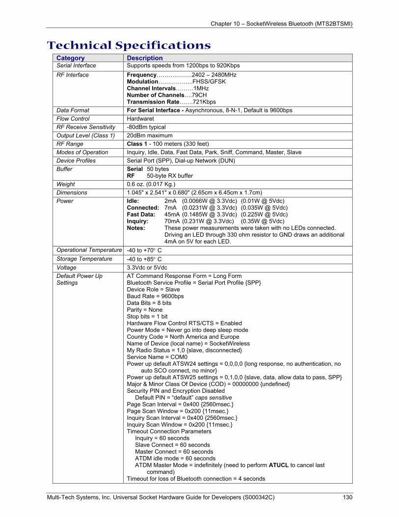
Chapter 10 – SocketWireless Bluetooth (MTS2BTSMI)
Multi-Tech Systems, Inc. Universal Socket Hardware Guide for Developers (S000342C) 130
Technical Specifications Category Description Serial Interface Supports speeds from 1200bps to 920Kbps RF Interface Frequency………………2402 – 2480MHz
Modulation……………...FHSS/GFSK Channel Intervals………1MHz Number of Channels….79CH Transmission Rate…….721Kbps
Data Format For Serial Interface - Asynchronous, 8-N-1, Default is 9600bps Flow Control Hardwaret RF Receive Sensitivity -80dBm typical Output Level (Class 1) 20dBm maximum RF Range Class 1 - 100 meters (330 feet) Modes of Operation Inquiry, Idle, Data, Fast Data, Park, Sniff, Command, Master, Slave Device Profiles Serial Port (SPP), Dial-up Network (DUN) Buffer Serial 50 bytes
RF 50-byte RX buffer Weight 0.6 oz. (0.017 Kg.) Dimensions 1.045" x 2.541" x 0.680" (2.65cm x 6.45cm x 1.7cm) Power Idle: 2mA (0.0066W @ 3.3Vdc) (0.01W @ 5Vdc)
Connected: 7mA (0.0231W @ 3.3Vdc) (0.035W @ 5Vdc) Fast Data: 45mA (0.1485W @ 3.3Vdc) (0.225W @ 5Vdc) Inquiry: 70mA (0.231W @ 3.3Vdc) (0.35W @ 5Vdc) Notes: These power measurements were taken with no LEDs connected. Driving an LED through 330 ohm resistor to GND draws an additional
4mA on 5V for each LED. Operational Temperature -40 to +70° C Storage Temperature -40 to +85° C Voltage 3.3Vdc or 5Vdc Default Power Up Settings
AT Command Response Form = Long Form Bluetooth Service Profile = Serial Port Profile SPP Device Role = Slave Baud Rate = 9600bps Data Bits = 8 bits Parity = None Stop bits = 1 bit Hardware Flow Control RTS/CTS = Enabled Power Mode = Never go into deep sleep mode Country Code = North America and Europe Name of Device (local name) = SocketWireless My Radio Status = 1,0 slave, disconnected Service Name = COM0 Power up default ATSW24 settings = 0,0,0,0 long response, no authentication, no
auto SCO connect, no minor Power up default ATSW25 settings = 0,1,0,0 slave, data, allow data to pass, SPP Major & Minor Class Of Device (COD) = 00000000 undefined Security PIN and Encryption Disabled Default PIN = “default” caps sensitive Page Scan Interval = 0x400 2560msec. Page Scan Window = 0x200 11msec. Inquiry Scan Interval = 0x400 2560msec. Inquiry Scan Window = 0x200 11msec. Timeout Connection Parameters Inquiry = 60 seconds Slave Connect = 60 seconds Master Connect = 60 seconds ATDM idle mode = 60 seconds ATDM Master Mode = indefinitely (need to perform ATUCL to cancel last
command) Timeout for loss of Bluetooth connection = 4 seconds
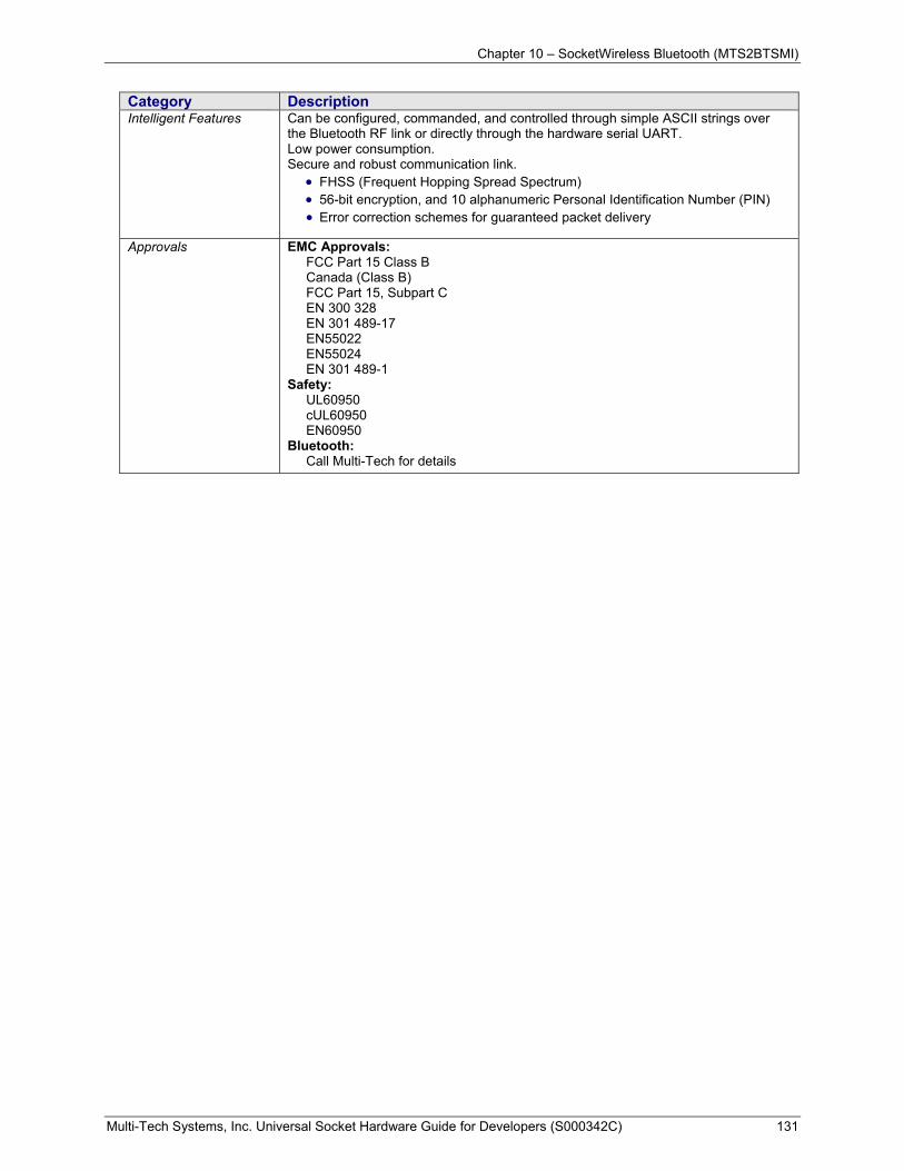
Chapter 10 – SocketWireless Bluetooth (MTS2BTSMI)
Multi-Tech Systems, Inc. Universal Socket Hardware Guide for Developers (S000342C) 131
Category Description Intelligent Features Can be configured, commanded, and controlled through simple ASCII strings over
the Bluetooth RF link or directly through the hardware serial UART. Low power consumption. Secure and robust communication link.
• FHSS (Frequent Hopping Spread Spectrum) • 56-bit encryption, and 10 alphanumeric Personal Identification Number (PIN) • Error correction schemes for guaranteed packet delivery
Approvals EMC Approvals: FCC Part 15 Class B Canada (Class B) FCC Part 15, Subpart C EN 300 328 EN 301 489-17 EN55022 EN55024 EN 301 489-1
Safety: UL60950 cUL60950 EN60950
Bluetooth: Call Multi-Tech for details
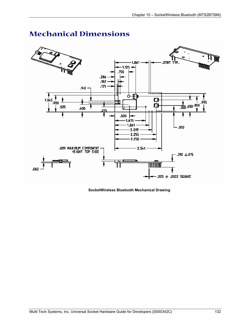
Chapter 10 – SocketWireless Bluetooth (MTS2BTSMI)
Multi-Tech Systems, Inc. Universal Socket Hardware Guide for Developers (S000342C) 132
Mechanical Dimensions
SocketWireless Bluetooth Mechanical Drawing
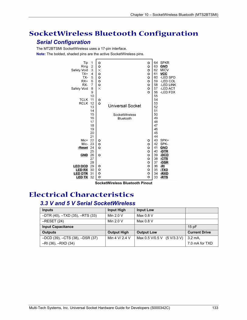
Chapter 10 – SocketWireless Bluetooth (MTS2BTSMI)
Multi-Tech Systems, Inc. Universal Socket Hardware Guide for Developers (S000342C) 133
SocketWireless Bluetooth Configuration Serial Configuration The MT2BTSMI SocketWireless uses a 17-pin interface. Note: The bolded, shaded pins are the active SocketWireless pins.
SocketWireless Bluetooth Pinout
Electrical Characteristics 3.3 V and 5 V Serial SocketWireless
Inputs Input High Input Low –DTR (40), –TXD (35), –RTS (33) Min 2.0 V Max 0.8 V –RESET (24) Min 2.0 V Max 0.8 V Input Capacitance 15 pF Outputs Output High Output Low Current Drive –DCD (39), –CTS (38), –DSR (37) –RI (36), –RXD (34)
Min 4 V/ 2.4 V Max 0.5 V/0.5 V (5 V/3.3 V) 3.2 mA, 7.0 mA for TXD
Chapter 10 – SocketWireless Bluetooth (MTS2BTSMI)
Multi-Tech Systems, Inc. Universal Socket Hardware Guide for Developers (S000342C) 134
Application Notes
Example of a Master Discovery/Connection Sequence From Power Up and No Connection
1. Verify local device is Master in Data Mode. Sent: ATSi,7 <cr_lf> Reply: <cr_lf>1,1,0,0<cr_lf>
2. If not Master, set to Master and Data Mode. Sent: ATSW25,1,1,0,0 <cr_lf> Reply: <cr_lf>OK<cr_lf>
3. Perform an Inquiry to obtain BT_Addresses (unless it is already known). Sent: ATMC <cr_lf> // Places Radio in Command Mode Reply: <cr_lf>OK<cr_lf> Sent: ATUCL // Clears radio state Reply: <cr_lf>OK<cr_lf> Sent: ATDI,1,00000000 Class of Device<cr_lf> // Looks for only one Bluetooth device Reply: <cr_lf>00A0961F2023,00000104,SOCKETWIRELESS<cr_lf>DONE<cr_lf>CONNECT <cr_lf>
4. Perform a Master Connect over SPP using the BT_Address. Sent : ATDM, 00A0961F2023,1101<cr_lf> // SPP connection Reply:<cr_lf>CONNECT,00A0961F008F <cr_lf> // Returns Slave BT address radios is in data
mode 5. Place radio into Fast Data Mode.
Sent : ATMC <cr_lf> // Places Radio in Command Mode Reply:<cr_lf>OK<cr_lf> Sent : ATMF<cr_lf> // Places radio in Fast Data Mode Reply:<cr_lf>OK<cr_lf>
6. Send Data.
Note about Sending Commands from the Slave When the Slave Connects in Fast Data Mode (ATSW25/or issuing ATMF) All valid AT commands sent through the Slave's UART will be interpreted and responded by the Master as if it were the local Slave radio. Basically, in this configuration from the Slave end, you can obtain status and configure the remote Master radio. This is a unique feature that may be useful in some applications, but it can be confusing if you think you are talking to the Slave.
To Get Out of Data Mode and Check Status 1. Delay at least 50 milliseconds; this could be less or more. 2. Perform a Set Command Mode.
Sent : ATMC<cr_lf> Reply:<cr_lf>OK<cr_lf>
3. Delay at least 50 milliseconds. 4. Check Status, perform a Disconnect …
Sent : AT<cr_lf> Reply:<cr_lf>OK<cr_lf>
Note about Being Connected in Fast Data Mode If connected in Fast Data Mode, it is necessary to reset the device to break the connection.
Chapter 10 – SocketWireless Bluetooth (MTS2BTSMI)
Multi-Tech Systems, Inc. Universal Socket Hardware Guide for Developers (S000342C) 135
Example of a Slave Command Sequence From Power Up:
1. Check and verify Communication to Slave. Sent : AT<cr_lf> Reply:<cr_lf>OK<cr_lf>
2. Get information on Slave Bluetooth address. Sent : ATSi,1<cr_lf> Reply: 12-digit address <cr_lf>OK<cr_lf>
3. Set Slave to automatically connect in Fast Data Mode on Bluetooth connection. Sent : ATSW25,0,0,0,0 <cr_lf> Reply:<cr_lf>OK<cr_lf>
4. Either cycle power or send ATURST. Note: This command sequence assumes the radio is in factory default in which it automatically comes up and is connectable as a Slave from a Master request.
Changing Configuration Parameters, such as the Bluetooth Name, Service Name, Class of Device, and Serial Port settings can be viewed and configured. This can be done locally through the serial port UART or from a remote Bluetooth RF link. To configure the SocketWireless Bluetooth device, the device must be in command mode by issuing ATMC. While in command mode, the SocketWireless Bluetooth device will accept ASCII bytes as commands. You can use the developer board and the RS-232 cable to connect to a PC and pass ASCII characters through the terminal to the SocketWireless Bluetooth device. The communications settings should match the settings used when the SocketWireless Bluetooth device connects. For example, the defaults are:
9600bps 8 bits No Parity 1 stop bit Hardware flow control enabled.
Once you change these parameters, you have the option to store them permanently in the non-volatile memory. Run your favorite terminal emulator, HyperTerminal, or other program.
• Type AT on your screen and follow it with a carriage return <cr_lf>. You should see "OK" returned to you. This will verify that your cable and communications settings are correct. When the SocketWireless device is not connected to another Bluetooth device, you can type the AT commands directly into the SocketWireless' UART; e.g., you do not have to type ATMC to change from data mode to command mode.
• Now you can enter any of the AT commands discussed in the following sections. Follow these commands by <cr_lf>. Valid commands will return an "OK" or a valid response. Invalid commands will reply ERROR.
• To return to data mode, type ATMD. You can now pass or receive data from a remote connected Bluetooth device.
Notes: • If you change communications parameter settings, remember to change your terminal or emulator
communications settings to correspond to the newly created parameter settings. • AT commands will not echo back to the terminal.
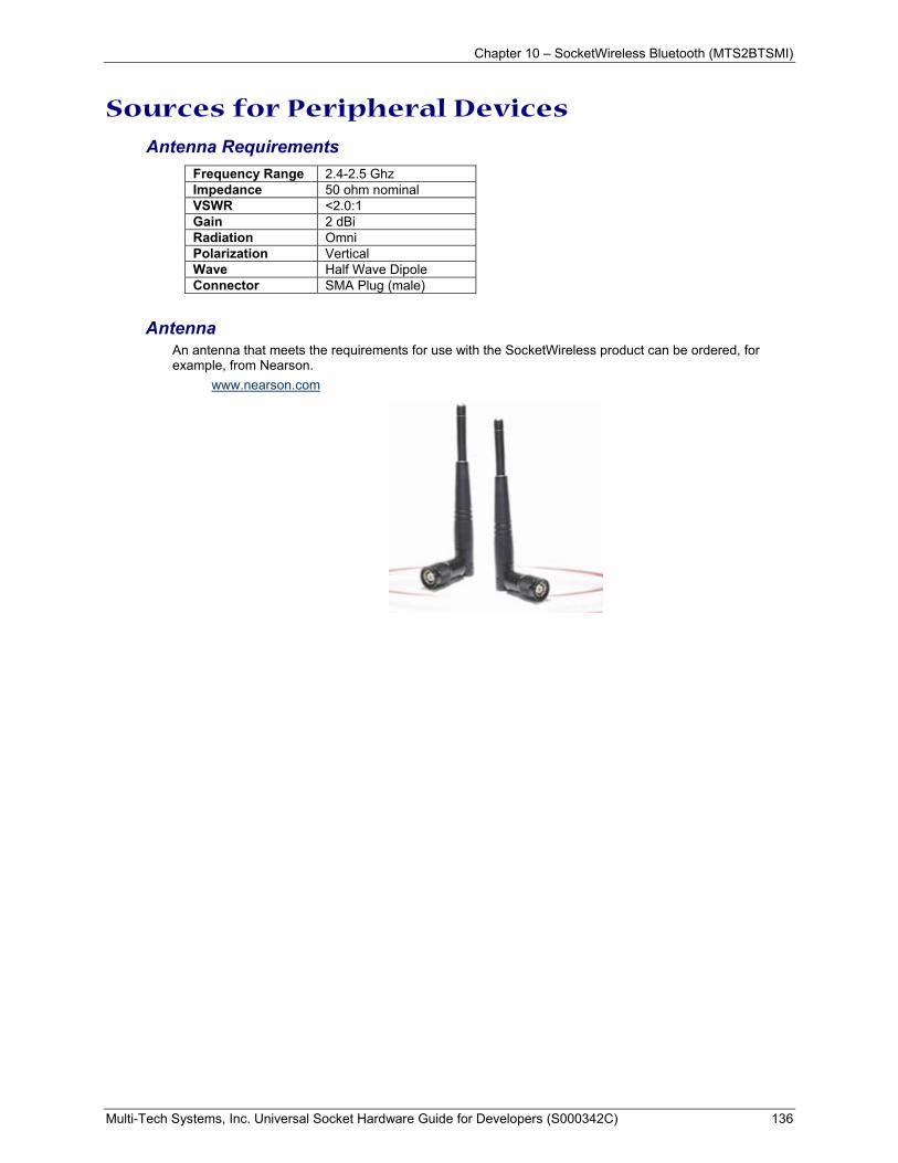
Chapter 10 – SocketWireless Bluetooth (MTS2BTSMI)
Multi-Tech Systems, Inc. Universal Socket Hardware Guide for Developers (S000342C) 136
Sources for Peripheral Devices
Antenna Requirements Frequency Range 2.4-2.5 Ghz Impedance 50 ohm nominal VSWR <2.0:1 Gain 2 dBi Radiation Omni Polarization Vertical Wave Half Wave Dipole Connector SMA Plug (male)
Antenna An antenna that meets the requirements for use with the SocketWireless product can be ordered, for example, from Nearson.
www.nearson.com
Index
Multi-Tech Systems, Inc. Universal Socket Hardware Guide for Developers (S000342C) 137
Index
5 5 V/3.3 V Jumper .....................................................17
A AT Commands Reference Guides .............................9 AT&T wireless ..........................................................36
B Bluetooth Configurations, Changing.......................135 Bluetooth technology..............................................129
C Cleaning Safety Standards ....................................126 Cleaning the Wireless SocketModem ....................119
D Design Considerations .............................................13 Developer Board ......................................................17 Developer Board Schematics.....18, 19, 20, 21, 22, 23 Developer Board, MT128SMI.................................106 Developer Kit
MT128SMI..........................................................102 MT2456SMI..........................................................80 MT2456SMI-IP .....................................................88 MT5600/5656SMI .................................................42 MT5634SMI..........................................................63 SocketEthernet IP.................................................96 SocketModem GPRS .........................................112 SocketWireless with Bluetooth ...........................129 Wireless CDMA ..................................................122
E Electrical Characteristics
MT128SMI (ISDN) ..............................................105 MT2456SMI-22.....................................................84 MT2456SMI-IP .....................................................92 MT5600/5656SMI .................................................47 MT5634SMI..........................................................68 SIM Interface ......................................................117 SocketEthernet IP.................................................99 SocketWireless with Bluetooth ...........................133 Wireless CDMA ..................................................125 Wireless GSM/GPRS .........................................116
Electromagnetic Interference Considerations ..........14 EMC, Safety, and R&TTE Directive Compliance......28
F Fax Commands Reference Guides ............................9 FCC Regulations......................................................28 Firmware Upgrade ...................................................30 Flash Programming Protocol....................................33
Flash Upgrade..........................................................30 Flash Upgrade Example.....................................31, 32
H Handling Precautions ...............................................17
I Internal Registers .....................................................72 International Modem Restrictions.............................28 Interrupt Sources and Reset Control Table
MT5600SMI..........................................................53 MT5634SMI..........................................................73
L Labeling the Product ................................................25 Legacy Voice Modem...............................................46
M Mechanical Dimensions
SocketModem GSM/GPRS ................................114 SocketWireless Bluetooth...................................132 Universal Socket...................................................15 Wireless CDMA ..................................................124
Microphone and Speaker MT5656SMI.....................60 Mobile PhoneTools ........................................119, 126 MT128SMI Interface...............................................105 MT128SMI Schematics ..................107, 108, 109, 110
N New Zealand Telecom Warning Notice....................29
O Ordering Replacement Parts....................................39
P Parallel Interface
MT5600SMI..........................................................49 MT5634SMI..........................................................70
Parallel Interface Register Table MT5600SMI..........................................................50 MT5634SMI..........................................................72
Parallel Pin Configurations MT5600/5656SMI .................................................45 MT5634SMI..........................................................67
Peripheral Devices SocketWireless with Bluetooth ...........................136 Wireless CDMA ..................................................127 Wireless GSM/GPRS .........................................119
Index
Multi-Tech Systems, Inc. Universal Socket Hardware Guide for Developers (S000342C) 138
Pin Configurations
MT128SMI (ISDN) ..............................................104 MT2456SMI-22.....................................................83 MT2456SMI-IP .....................................................91 MT5600SMI..........................................................44 MT5634SMI..........................................................66 SocketEthernet IP.................................................99 SocketModem GSM/GPRS ................................115 SocketWireless with Bluetooth ...........................133
Product Ordering Information MT128SMI..........................................................102 MT2456SMI-22.....................................................80 MT2456SMI-IP .....................................................88 MT5600/5656SMI .................................................41 MT5634SMI..........................................................63 SocketEthernet IP.................................................96 SocketModem GPRS .........................................112 SocketWireless with Bluetooth ...........................129 Wireless CDMA ..................................................122
Programmable Baud Rates Table MT5600SMI..........................................................58 MT5634SMI..........................................................76
R Radio Characteristics .....................................119, 127 Recommended Parts .............................61, 78, 86, 94 Repair ......................................................................38 Replacement Parts...................................................39
S Safety Considerations ..............................................13 SIM Interface..........................................................118 Sleep Mode..............................................................65 Software Features SocketEthernet IP ......................98 Soldering Safety Standards ...................................126 Soldering the Wireless SocketModem ...................119 South African Statement, Regulations .....................29 Speakerphone..............................................12, 41, 46 Sprint wireless..........................................................36
T Technical Specifications
MT128SMI (ISDN) ..............................................103 MT2356SMI-22.....................................................81 MT2456SMI-IP .....................................................89 MT5600/5656SMI .................................................42 MT5634SMI..........................................................64 SocketEthernet IP.................................................97 SocketModem GPRS .........................................113 SocketWireless with Bluetooth ...........................130 Wireless CDMA ..................................................123
Telecom Approvals ..................................................24 Telephone Answering Machine..........................65, 90 Timing Requirements
MT5600SMI..........................................................48 MT5634SMI..........................................................69
Tip and Ring Interface MT2456SMI-22.....................................................85 MT2456SMI-IP .....................................................93 MT5600/5656SMI .................................................59 MT5634SMI..........................................................77 SocketEthernet IP...............................................100
U Universal Pin Locations............................................10 Universal Socket Design ............................................8
V Verizon wireless .......................................................37 Voice
Speakerphone ..........................................12, 41, 46 Telephone Answering Machine ............................65
Voice Commands Reference Guides .........................9
W Warranty ..................................................................38 Wireless account activation......................................36 Wireless CDMA Interfaces .....................................126 Wireless GSM/GPRS Interfaces ............................118