Embed Size (px)
Citation preview

UNIVERSITY OF CALIFORNIA RIVERSIDE
Optoelectronics Investigations of Electron Dynamics in 2D-TMD Semiconductor Heterostructure Photocells: From Electron-Hole Pair Multiplication to Phonon Assisted
Anti-Stokes Absorption
A Dissertation submitted in partial satisfaction of the requirements for the degree of
Doctor of Philosophy
in
Physics
by
FatemehBarati
December 2018
Dissertation Committee: Dr. Nathaniel Gabor, Chairperson Dr. Yongtao Cui Dr. Vivek Aji

Copyright by FatemehBarati
2018

TheDissertationofFatemehBaratiisapproved:
CommitteeChairperson
UniversityofCalifornia,Riverside

iv
ACKNOWLEDGEMENT
I would like to thank my advisor, Prof. Nathaniel Gabor, for the patient guidance,
encouragement and advices he has provided over my years of being his student. Working
with him has been a wonderful experience for me for I not only learned so much from his
intellect but also from his friendly and kind manner life lessons, thank you.
I would like to thank Prof. Roland Kawakami for giving me this excellent opportunity of
becoming a graduate student at UCR and trusting in me.
I would like to thank Prof. Vivek Aji and Prof. Yongtao Cui for their great ideas and
collaborations toward improving my work and their kind support for my future academic
goals, Prof. Roger Lake and Dr. Shanshan Su for their theoretical collaboration in part of
this work. I’m grateful for my friends and colleagues at QMOlab, Dennis, Max, Trevor,
Jacky, and Jed for without their friendship and support the completion of this work would
have been all the more difficult. I’m grateful for everyone that has helped me throughout
my journey to this day including lab facilities and other research groups here at UCR.
Finally I would like to thank my family, my Mom, my Dad, and my only sister Zahra,
and above all Mir, I’m very lucky to have you in my life, and experience the true
happiness around you, thank you.

v
DEDICATION
To my one and only best friend Mir Shahsavar I couldn’t have done this without your support
to my beloved parents and to my little sister Zahra

vi
ABSTRACT OF THE DISSERTATION
Optoelectronics Investigations of Electron Dynamics in 2D-TMD Semiconductor Heterostructure Photocells: From Electron-Hole Pair Multiplication to Phonon Assisted
Anti-Stokes Absorption
by
Fatemeh Barati
Doctor of Philosophy, Graduate Program in Physics University of California, Riverside, December 2018
Prof. Nathaniel Gabor, Chairperson
Efficient electron-hole (e-h) pair multiplication could lead to highly sensitive
photodetectors, electroluminescent emitters, and improved-efficiency photovoltaic
devices. In this thesis, using advanced optoelectronic measurements, I discuss the
discovery of highly efficient multiplication of interlayer electron-hole pairs at the
interface of ultrathin tungsten diselenide / molybdenum diselenide integrated into field-
effect heterojunction devices. Electronic transport measurements of the interlayer current-
voltage characteristics indicate that interlayer electron-hole pairs are generated by hot
electron impact excitation at temperatures near T = 300 K. By exploiting this highly
efficient interlayer e-h pair multiplication process, we demonstrated near-infrared
optoelectronic devices that exhibit 350% enhancement of the optoelectronic responsivity
at microwatt power levels.
We extend our understanding of these materials by conducting spatially and
spectrally resolved imaging of the device photoresponse at low temperatures. Under

vii
carefully tuned experimental conditions, we observe phonon assisted anti-stokes
absorption near the interlayer exciton edge of the van der Waals semiconductor
heterostructure composed of tungsten diselenide and molybdenum diselenide. At low
photon energies near 1 eV, we observed a strong photocurrent peak with several low
energy echoes spaced by 30 meV below the fundamental absorption feature. We attribute
this highly unusual absorption to high-harmonic anti-stokes absorption; The alignment of
the exciton dipole moment to the atomic displacement of the out-of-plane optical phonon
modes gives rise to resonant absorption features akin to vibronic transitions in molecules.
The anti-stokes process is the first and most critical step toward laser cooling of atomic
layer semiconductors. Moreover, it could enhance the efficiency of next generation
photovoltaics, since it converts vibrational energy into electronic excitations using
photons with energies that are lower than the band gap.

viii
TABLE OF CONTENTS
Acknowledgements iv Dedication v Abstract vi Chapter 1: Introduction and Background 1.1 Introduction: Electron-Hole Pair Production and Annihilation 1 1.2 Semiconductor P-N Junctions 2 1.3 Conventional P-N Junction Diodes Band Diagram 2 1.4 Conventional P-N Junction Photodiodes 6 References 8 Chapter 2: Theory of 2DEG and 2D-Transition Metal Dichalcogenides Band Structure 2.1 Introduction 9 2.2 Electronic Structure 10 2.3 Electronic Band Structure of 2L-WSe2/MoSe2 13 2.4 Transport in Conventional Two Dimensional Electron Gas (2DEG) 19 2.4.1 Band Diagram of 2DEG 21 2.4.2 Density of States of 2DEG 23 2.5 Density of States in Transition Metal Dichalcogenides 26 References 28 Chapter 3: Device Fabrication 3.1 Introduction 30 3.2 Wafer Preparation 30 3.3 Exfoliation 31 3.4 Stacking 2D-TMD atomic layers 35 3.5 Device Fabrication 37 References 40 Chapter 4: instrumentation: Low Temperature Broadband Photocurrent Scanning Microscope 4.1 Introduction 41 4.2 Light-Matter Interaction at the Nanoscale 41

ix
4.3 The Supercontinuum Scanning Photocurrent Spectroscopy Microscope 42 4.4 Electronic Transport Experiment Instrumentation 45 4.5 Optical Imaging Microscopy Instrumentation 50 4.6 Optoelectronic Experiment Instrumentation 53 4.6.1 Fianium Supercontinuum Ultrafast Fiber Lasers 53 4.6.2 Princeton Instruments Monochromator 55 4.6.3 Getting Light Into A Monochromator 58 4.6.4 Gathering Spectrally Resolved Light Out Of Monochromator 61 4.6.5 Dual-Axis Scanning Galvo System 63 4.6.6 Spatially And Spectrally Resolved Laser Excitations 66 4.6.7 Power Dependence Experiments 70 4.7 Running Experiments Through Software 72 References 74 Chapter 5: Basic Optical Characterization of TMDs Heterostructures 5.1 Introduction 75 5.2 Raman Spectroscopy 76 5.3 Photoluminescence Spectroscopy 80 5.4 Photocurrent and Differential Reflection Spectroscopy 81 References 84 Chapter 6: Hot Carrier-Enhanced Interlayer Electron–Hole Pair Multiplication in 2D Semiconductor Heterostructure Photocells 6.1 Introduction 85 6.2 2D-TMD Semiconductors Junction Characteristics 86 6.3 Gate Voltage Dependence of I-VSD Characteristics of 2L-WSe2/MoSe2 90 6.4 Temperature Dependence of I-VSD Characteristics of 2L-WSe2/MoSe2 92 6.5 Interlayer Electron Transport of 2L-WSe2/MoSe2 95 6.5.1 Forward Bias Characteristics 96 6.5.2 Reverse Bias Characteristics 99 6.6 Gate and Temperature Dependence of dlogI/dVG of 2L-WSe2/MoSe2 102 6.7 Power Dependence of I-VSD Characteristics of 2L-WSe2/MoSe2 104 6.8 Comparison of the Model to Experimental Data 108 6.9 Photoresponse of the Atomic Layer Hetero-Junction 110 6.10 2D-TMD N+-N Junction Characteristics 111 References 114 Chapter 7: Phonon-Assisted Antistokes Upconversion in a 2D-TMD Heterostructure 7.1 Laser Cooling of Semiconductors 115

x
7.2 Preliminary Optical Characterizations 116 7.3 Spectral Imaging of High-Energy Excitation 119 7.4 Spectral Imaging of Low-Energy Excitation 120 7.5 2D-TMD P-N Junction Characteristics 122 7.5 Phonon-Assisted Antistokes Shift 125 References 128 Chapter 8: Conclusion 129

xi
LIST OF FIGURES
Figure 1.1. P-N junction at equilibrium. 3 Figure 1.2. Schematic representations of depletion layer width and energy band 4 diagram of a P-N junction under various biasing conditions. Figure 1.3. Current-voltage characteristics of a typical silicon P-N junction. 5 Figure 1.4. The semiconductor PN junction photodiode. 7 Figure 2.1. Constituent elements of transition metal dichalcogenides are 10 highlighted in the periodic table. Figure 2.2. Various atomic structures of TMDs. 11 Figure 2.3. Two-dimensional Brillouin zone (BZ) of MX2. 13 Figure 2.4. Schematics of the MoSe2/2L-WSe2 heterostructure. 15 Figure 2.5. Schematics of the MoSe2/2L-WSe2 electronic band structure. 18 Figure 2.6. Conduction and valence band line-up at a junction between an 21 N-type AlGaAs ad intrinsic GaAs. Figure 2.7. Dispersion relation, band diagram in real space and momentum space. 22 Figure 2.8. Energy band diagram of a 2D-TMD material with hyperbolic 28 band structure. Figure 3.1. Exfoliation process. 34 Figure 3.2. Optical images of a few exfoliated layers of WSe2, and MoSe2. 34
Figure 3.3. Transfer microscope and device schematics. 35
Figure 3.4. Schematic illustration and optical images of the dry-transfer process. 37
Figure 3.5. Optical images of devices. 39
Figure 3.6. Optical images of a fabricated device with different magnifications 39 from 5x to 100x.

xii
Figure 4.1. Schematic diagram of the supercontinuum scanning 44 photocurrent spectroscopy microscope (SSPSM). Figure 4.2. Photograph from the optical cryostat. 45 Figure 4.3. Photograph of wire bonding the electrical pads of the device. 47 Figure 4.4. Schematics of the atomic layer device. 47
Figure 4.5. Photographs and the electrical circuit diagram of the equipment 50 used for electronic experiments.
Figure 4.6. Optical imaging microscopy. 52
Figure 4.7. Schematic of the imaging microscope. 52
Figure 4.8. A typical supercontinuum spectrum 54
Figure 4.9. Schematics of the ray diagram of SP-2300 monochromator. 57
Figure 4.10. Monochromator Control Software & Grating efficiency 57 curves of SP2300. Figure 4.11. Diagram of the lens system required for getting light into the 60 entrance slit of MC. Figure 4.12. Getting light into the MC. 60 Figure 4.13. Optical diagram for getting light out of the MC. 62
Figure 4.14. Getting light out of the MC. 62
Figure 4.15. Scanning galvo system. 65
Figure 4.16. Schematics of the scanning Gaussian beam over the surface of 66 the sample.
Figure 4.17. Diffraction limited beam spot to the cryostat. 69
Figure 4.18. Power dependence experiment. 71
Figure 4.19. Profile of the custom-written SSM software. 73
Figure 5.1. Schematic drawing of the four Raman active and two inactive modes. 77
xiii
Figure 5.2. Optical images, Raman spectroscopy, and PL spectroscopy of devices 79
Figure 5.3. Device geometry and the PL spectra of the 2D semiconductor 81 heterostructure device.
Figure 5.4. Differential reflection and photocurrent spectroscopy 83 measurements of Device.
Figure 6.1. Various heterostructure band alignments. 86 Figure 6.2, Schematics of the MoSe2/2L-WSe2 electronic band structure under 89 different values of VSD and VG. Figure 6.3. Gate voltage dependence of the I-VSD and dI/dVSD characteristics in 91 the 2D N+-N heterojunction device. Figure 6.4. Temperature dependence of the interlayer I-VSD characteristics. 94 Figure 6.5. Schematics of TMD band structure and interlayer electronic transport. 98
Figure 6.6. Gate voltage, source-drain voltage, and temperature 103 dependence of dlogI/dVG in the atomic layer semiconductor heterostructure device. Figure 6.7, Interlayer photocurrent characteristics and multiplication 106 enhancement in the 2D heterojunction photocell.
Figure 6.8. Interlayer current-voltage characteristics in the transport regime 109 near the onset to NDC.
Figure 6.9. Wavelength dependence of the photocurrent-voltage characteristics 111 at T = 300 K.
Figure 6.10. Band structure, and current-voltage characteristics of the 2D 113 semiconductor heterostructure device. Figure 7.1. Device configuration, and Raman Spectra. 118
Figure 7.2. Gate voltage dependence of the excitation photon energy of the 120 P-N atomic layer heterostructure under high excitations.
Figure 7.3. Low energy excitations. 122
Figure 7.4. Band structure, and interlayer charge transfer at the P-N junction of 124 2L-WSe2/MoSe2.

xiv
Figure 7.5. Gate voltage dependence of I-VSD characteristics under illumination 124 and in the absence of light. Figure 7.6. Band profile, two-level system transitions, and E-K diagram 127 of the heterointerface of 2L-WSe2/MoSe2

1
CHAPTER 1
INTRODUCTION AND BACKGROUND
1.1 Introduction: Electron-Hole Pair Production and Annihilation
When external energy is supplied to a conventional semiconductor, the valence
band electrons may jump to the conduction band leaving behind a vacancy in the valence
band called a hole. The electron and the newly formed hole, whose formation required
sufficient excess energy to raise the electron across the band gap of the semiconductor,
combine to form an electron-hole (e-h) pair. The excess energy required for e-h pair
generation can be supplied from a heat source, from high energy charge carriers, or from
the interaction of light with the semiconductor. In the inverse process, the excited
electron can release the gained energy and recombine back to the conduction band
through a process called e-h pair annihilation. Conduction band electrons may also gain
sufficient kinetic energy to collide with carriers in the valence band generating additional
electron-hole pair via impact ionization1. Efficient e-h pair generation results in extra
charge carriers and thus could lead to highly sensitive photodetectors, electroluminescent
emitters, and improved-efficiency photovoltaic devices. In this thesis, I discuss
optoelectronic transport and e-h pair generation in 2D-TMD semiconductors
heterostructures configured into P-N and N-N heterojunction devices. For comparison to
modern technology, it is informative to first present the basic characteristics and behavior
of conventional semiconductors.

2
1.2 Semiconductor P-N Junctions
Semiconductor P-N junctions are essential building blocks for electronic and
optoelectronic devices. In conventional P-N junctions, regions depleted of free charge
carriers form on either side of the junction, generating built-in potentials associated with
uncompensated dopant atoms. Carrier transport across the junction occurs by diffusion
and drift processes influenced by the spatial extent of this depletion region. With the
advent of atomically thin van der Waals materials and their heterostructures, it is now
possible to realize a P-N junction at the ultimate thickness limit. Van der Waals junctions
composed of P- and N-type semiconductors - each just one-unit cell thick - are predicted
to exhibit completely different charge transport characteristics than bulk heterojunctions.
In this thesis we aim to study the optoelectronic characteristics of atomically thin
heterojunctions composed of transition metal dichalcogenides and to do so it is important
to first understand the basic working principles of a conventional P-N junction. In this
chapter introduce the conventional P-N junction. After describing the basic solid state
physics of two-dimensional materials (Chapter2), we then present 2D van der Waals
junctions and photo junctions composed of transition metal dichalcogenides in Chapter 6.
1.3 Conventional P-N Junction Diodes Band Diagram
In conventional materials, when P- and N-type semiconductors are jointed together, the
large carrier concentration gradients at the junction cause carrier diffusion. Holes from
the p-side diffuse into the N-side, and electrons from the n-side diffuse into the P-side. As
holes continue to leave the P-side, some of the negative acceptor ions (NA-) near the

3
junction are left uncompensated, since the acceptors are fixed in the semiconductor
lattice, whereas the holes are mobile. Similarly, some of the positive donor ions (ND+)
near the junction are left uncompensated as the electrons leave the n-side. Consequently,
a negative space charge forms near the P-side of the junction and a positive space charge
forms near the n-side. This phenomenon creates a space charged region at the junction, a
region that is depleted of mobile carriers, called the depletion region1. This space charge
region creates an electric field that is directed from the positive charge toward the
negative charge, as indicated in Fig. 1.1b at top.
The electric field is in the direction opposite to the diffusion current for each type
of charge carrier. The lower illustration of Fig. 1.1b shows that the hole diffusion current
flows from left to right, whereas the hole drift current due to the electric field flows from
right to left.
Figure 1.1. P-N junction at equilibrium. a, Uniformly doped P-type and N-type semiconductors before the junction is formed. b, The electric field in the depletion region and the energy band diagram of a P-N junction in thermal equilibrium.

4
The electron diffusion current also flows from left to right, whereas the electron
drift current flows in the opposite direction. The diffusion of carriers continues until the
drift current balances the diffusion current, then reaching a thermal equilibrium as
indicated by a constant Fermi energy. The equilibrium energy band diagram, shown again
in Fig. 1.2a, illustrates that the total electrostatic potential across the junction is Vbi. The
corresponding potential energy difference from the P-side to the n-side is approximately
qVbi. Forward and reverse bias conditions are illustrated in Fig. 1.2 b, & c.
Figure 1.2. Schematic representations of depletion layer width and energy band diagram of a P-N junction under various biasing conditions. a, Thermal equilibrium condition. b, Forward bias condition. c, Reverse bias condition.

5
The most important characteristic of P-N junctions is that they rectify, that is, they
allow current to flow easily in only one direction. Figure 1.3 shows the current-voltage
characteristics of a typical silicon P-N junction.
Forward Bias:
If we apply a positive voltage Vf to the p-side with respect to the n-side, the P-N
junction becomes forward-biased, as shown in Fig. 1.2b. The total electrostatic potential
across the junction decreases by Vf and becomes Vbi- Vf. Thus, forward bias reduces the
depletion layer width2.
Reverse Bias:
By contrast, as shown in Fig, 1.2c, if we apply positive voltage VR to the N-side
with respect to the p-side, the P-N junction now becomes reverse-biased and the total
electrostatic potential across the junction increases by VR becoming Vbi + VR. Here, we
find that reverse bias increases the depletion layer width2.
Figure 1.3. Current-voltage characteristics of a typical silicon P-N junction.

6
1.4 Conventional P-N Junction Photodiodes
One of the interesting approaches to studying the interaction of light with matter
is through photo-sensitive diode devices. Because the PN junction is composed of
semiconducting materials, the minimum energy required to excite an electron from the
valence band to the conduction band is the band gap energy EGAP. The electronic
potential energy profile and schematic device characteristics are shown in figure 1.4
The P-N junction is an important electronic and optoelectronic element in modern
electronics, yet also provides an experimental platform to study light-matter interactions
in novel semiconductor materials such as atomically thin van der Waals materials. If a
photon whose energy exceeds the band gap energy is incident on the P-N junction, it
creates an electron-hole pair that is separated by the electric field and collected at the
contacts. This leads to additional current that offsets the dark current-voltage (I-V)
characteristic, illustrated in Fig. 1.4b. In forward bias, the amount of optical power
converted to electrical power generated in the device, P = I0V0, is the power conversion
efficiency. This is the basic operating principle of solar cell devices used for energy
harvesting. In reverse bias, the built-in field may become so strong that electrons and
holes are accelerated to high kinetic energies, giving rise to avalanche multiplication used
in highly sensitive photodetectors.

7
Figure 1.4. The semiconductor PN junction photodiode. a, Schematic potential energy diagram for electrons in a PN junction showing the potential energy barrier (or built-in electric field). An incident photon excites an electron-hole pair in the junction. The electron-hole pair is separated and collected at the device contacts. b, Typical current-voltage characteristics for a conventional PN junction. This figure is adapted from reference 3.

8
REFERENCES
1. Sze, M. & NG, K. K. Physics of Semiconductor Devices. (Wiley-Interscience publications, United States, 1963).
2. Datta, S., Electron Transport in Mesoscopic Systems. (Cambridge university Press, Cambridge, 1995).
3. Gabor, N. M. Extremely Efficient and Ultrafast: Electrons, Holes, and their Interactions in the Carbon Nanotube P-N Junction. (Cornell University, 2012).

9
CHAPTER 2
THEORY OF TRANSITION METAL DICHALCOGENIDES BAND STRUCTURE
2.1 Introduction
Transition metal dichalcogenides are a class of materials with stoichiometry MX2,
where M is a transition metal of group-IV, group-V or group-VI, and X represents a
chalcogen, such that one hexagonally packed layer of M atoms is sandwiched between
two layers of X atoms. The bulk of TMDs consist of stacked sheets of atomically thin
layers, each layer typically with a thickness of 6~7 Å. The intralayer M–X bonds are
predominantly covalent in nature, whereas the sandwich layers are coupled by weak van
der Waals forces thus allowing the crystal to easily cleave along the layer surface. The
properties of bulk TMDs are diverse, ranging from insulators such as HfS2,
semiconductors such as MoSe2 and WSe2, semimetals such as WTe2 and TiSe2, to true
metals such as NbS2 and VSe2. Exfoliation of these materials into atomically thin two-
dimensional crystals preserves their bulk properties, while new physical properties
emerge due to quantum confinement effects. Among them, monolayers of group-VI
transition metal dichalcogenides are of particular interest as a family of ultrathin
semiconductors1.
In this chapter we first present an intuitive description of the electronic band
structure of this class of 2D layered materials and then explicitly discuss some of the
10
exotic properties that emerge in them due to quantum confinement.
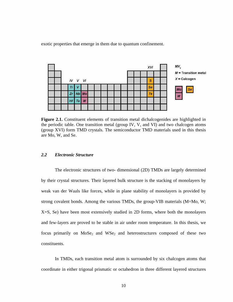
Figure 2.1. Constituent elements of transition metal dichalcogenides are highlighted in the periodic table. One transition metal (group IV, V, and VI) and two chalcogen atoms (group XVI) form TMD crystals. The semiconductor TMD materials used in this thesis are Mo, W, and Se.
2.2 Electronic Structure
The electronic structures of two- dimensional (2D) TMDs are largely determined
by their crystal structures. Their layered bulk structure is the stacking of monolayers by
weak van der Waals like forces, while in plane stability of monolayers is provided by
strong covalent bonds. Among the various TMDs, the group-VIB materials (M=Mo, W;
X=S, Se) have been most extensively studied in 2D forms, where both the monolayers
and few-layers are proved to be stable in air under room temperature. In this thesis, we
focus primarily on MoSe2 and WSe2 and heterostructures composed of these two
constituents.
In TMDs, each transition metal atom is surrounded by six chalcogen atoms that
coordinate in either trigonal prismatic or octahedron in three different layered structures

11
1T, 2H, and 3R (Figure 2.2 a, b). 1T is not as stable as the 2H and 3R phases for the two
group-VIB TMDs we are focusing on in this thesis. For the 2H and 3R phases, the
monolayer has the identical structure and the difference lies in the stacking order of the
monolayers in the layered structures2.
Figure 2.2. Various atomic structures of TMDs. a, Top view of an octahedral coordination of a TMD with transition atoms (red) and chalcogen atoms (blue) at the left and the polymorph structure at right, octahedron only has one form of 1T layered structure. b, Triangular prism coordination with 2H, and 3R structure and the polymorph structure. c, Side view of 1T, 2H, and 3R polytype structures. This figure is adapted from reference 3.

12
The 2H phase of bulk TMD crystals exhibits hexagonal symmetry, having two
monolayers per repeat unit, where the neighboring monolayers are rotated 180◦ with
respect to each other. The 3R phase has the rhombohedral symmetry, having three layers
per repeat unit, where the neighboring layers are translations of each other (Figure 2.2 c).
In general, thin film TMDs exfoliated from the natural crystals are mostly 2H stacking3.
In MX2 crystals with trigonal prism structure, we require three lattice parameters
a, b, and u to describe the crystal structure. As shown in Figure 2.2b, a = distance
between nearest neighbor in-plane M–M and X–X atoms, b= nearest neighbor M–X
separation, and u= distance between the M and X planes. The corresponding in-plane
hexagonal Brillouin zone contains the high-symmetry points Γ= (0,0), K= !!!!
(1,0),
M= !!!!
(0, √!!
) shown in figure 2.34. Using a1 and a2 the primitive vectors of the real 2D
lattice described by equation (2.1) shown in figure 2.2a, we can calculate the
corresponding reciprocal lattice vectors b1, and b2 according to equation (2.2) shown in
figure 2.3.
b= 7
12a , u= a2
a1!"!
= a2 3x"
+ y!"( )
a2!"!
= a2 − 3x"
+ y!"( ) (2.1)
b1!"!
= 2πa
33 Kx
! "!+K y
! "!⎛
⎝⎜
⎞
⎠⎟
b2!"!
= 2πa
− 33 Kx
! "!+K y
! "!⎛
⎝⎜
⎞
⎠⎟ (2.2)

13
Figure 2.3. Two-dimensional Brillouin zone (BZ) of MX2. The high symmetry points Γ, K, K’ and M are shown. Vectors b1 and b2 denote the in-plane reciprocal lattice vectors. Adapted from. Figure adapted from reference 4.
The six Q points in Figure 2.3 (which are not high symmetry points) correspond
to the approximate position of the edges of the conduction band in multi-layer TMD. In
monolayers, it is important to note that the conduction band minimum (CBM) and the
valence band maximum (VBM) are both located at the corners of the first BZ, where they
are considered as the only active band. In the next section, we present calculations of the
band structures that result from combining these unique crystal structures. We then use
this knowledge to understand the band structure near the corners of the BZ.
2.3 Electronic Band Structure of 2L-WSe2/MoSe2
When combined into heterostructures the transition metal dichalcogenides band
structure changes and forms a new band structure at the interface of the two materials.
This new band structure is completely distinguished from each of the individual layers,

14
just like a new semiconductor with its own band structure. Throughout this thesis, we
study the electronic band structure of a heterostructure composed of 2L-WSe2/MoSe2 at
the high symmetry points of K. In this section, we present detailed band structure
calculations of the new band structure that emerges in this unique combination of
materials.
As discussed in previous section, monolayers of TMD are formed by layers in
which the transition metal atom (W or Mo) is sandwiched between sulfur or selenium
atoms. The atomic model representing the heterostructure of a 2L-WSe2 stacked on top of
a layer of MoSe2 is illustrated in figure 2.4a. Figure 2.4b illustrates the atomic layer
heterostructure on a Si/SiO2 substrate with back gate and source and drain contacts. In the
remainder of this section the theoretical discussion on the electronic band structure of this
heterostructure is represented under applying positive and negative electric field between
the two layers.
Band dispersions and band gap energies of the MoSe2/2L-WSe2 heterostructure
including spin-orbit coupling (SOC) were calculated using the Vienna ab initio
simulation package (VASP)5-7 in the projected-augmented-wave method8. We used the
generalized gradient approximation (GGA) of the Perdew-Burke-Ernzerhof (PBE)9-11
form for the exchange correlation energy.

15
Figure 2.4. Schematics of the MoSe2/2L-WSe2 heterostructure. a, Schematic illustration of the atomic layer structure of a stack of 2L-WSe2 on a layer of MoSe2. b, Heterostructure integrated into a field effect transistor with source and drain contacts and a back-gate from underneath.
The van der Waals (vdW) interactions between the layers are accounted for by
using the DFT-D2 method of Grimme12. We set the kinetic energy cutoff for our
calculation at 500 eV. For all structural relaxations, the convergence tolerance on the
Hellmann-Feynman forces is less than 0.01 eV/Å. An 8×8×1 Γ-centered Monkhorst-Pack
k- point mesh is used for the 2D films. A vacuum layer of 20 Å is included in the
supercell in the z- direction to prevent interactions between the periodic repetitions of the
two-dimensional structure. With these settings, the lattice constant of MoSe2 is calculated
as 3.3247 Å and the lattice constant of WSe2 as 3.326 Å, so the lattice mismatch between
the two materials is less than 0.1%.
Our simulation results are consistent with the published lattice constants of the
two materials13,14. For the trilayer heterostructure, the lattice constant is 3.3254 Å. The
calculated vdW gap between MoSe2 and bilayer WSe2 is 3.15 Å (the vertical distance

16
between the Se and Se atoms), which is consistent with the published results of ref.15. The
thickness of trilayer system is 12.94 Å (the vertical distance between Mo to the furthest
W atom). The calculated PBE bandgaps of monolayer MoSe2 and bilayer WSe2 are 1.317
eV and 1.18 eV, respectively. Our calculated results are consistent with prior simulation
results16,17. Experimental measurements show that the bandgap of monolayer MoSe2 is
1.55 eV18, and the bandgap of bilayer WSe2 has an indirect bandgap of 1.26 eV19.
The band alignment and band structure of the combined trilayer TMD
heterostructure under different electric fields are calculated, and a small sample of band-
alignments are shown in Figure 2.5 below. Band structure calculations of the MoSe2/2L-
WSe2 heterostructure give an intrinsic type II heterojunction, and exhibit strong
qualitative and quantitative agreement with the band offset energies obtained from
electronic transport measurements. Figure 2.5 shows the calculated MoSe2/2L-WSe2
heterostructure band alignment under negative (Fig. 2.5a), zero (Fig. 2.5b), and positive
(Fig. 2.5c) applied electric field. The electric field is oriented perpendicular to the 2D
plane to simulate the electric field due to interlayer applied VSD.
Figure 2.5a shows the heterostructure band alignment under a negative VSD bias
voltage, which was calculated by applying a negative electric field of -0.2 eV/Å, pointing
from WSe2 to MoSe2. With this negative electric field the bandgap is a 0.73 eV direct
gap. For bilayer WSe2, the conduction band minimum (CBM) composed of dZ2
is at K,
while the valence band maximum (VBM) composed of W dx2-y2 and dxy is also at K. The
MoSe2 also has a direct gap at the K valley. The orbital composition is the same as WSe2.

17
Figure 2.5b shows the heterostructure bands with no applied electric field. Here
the band gap is an indirect 0.94 eV gap and shows features indicative of an intrinsic type
II heterojunction. The bandgap of bilayer WSe2 is 1.14 eV while the bandgap of MoSe2 is
1.25 eV. The CBM is at the K valley as set by MoSe2 , while the VBM is at the Γ valley
from WSe2. In the MoSe2 layer, the CBM is at K and the VBM is at Γ. The CBM is
composed of Mo dz2. The VBM is composed of dz2. In the WSe2 layer, the CBM is also at
K; the VBM is at the Γ valley. WSe2’s CBM is also composed of dz2 , while its VBM is
composed of dz2 . Figure 2.5c shows the band alignment of the heterostructure under
positive VSD, which was calculated by applying positive electric field 0.2 eV/Å.
From the heterostructure height of 2.0 nm, a direct correlation between eVSD and
electric field would give an approximate VSD value of VSD > 4 V. For N-type conduction,
the potential barrier is fully reduced, thus giving rise to current flow in high forward bias
(See section 3.9.1 for details). We note that, due to several regimes of device transport,
the quantitative changes of the band structure with electric field cannot be dependably
related to exact applied voltage. In Figure 2.5c, the minimum gap of 0.96 eV is
completely determined by WSe2. The CBM, which is composed of W’s dx2-y2 and dxy, is
at Σ, while the VBM composed of W’s dz2 is at the Γ valley. MoSe2 has direct gap with its
CBM and VBM both at K. The composition of the CBM of MoSe2 is Mo dz2; the VBM
composition of MoSe2 is dx2-y2 and dxy.

18
Figure 2.5. Schematics of the MoSe2/2L-WSe2 electronic band structure. a, b, c, Schematic illustration of the electronic band structure of the heterostructure under negative, zero, and positive electric field, respectively. Gray horizontal dashed lines show chemical potential of the individual layers, and the region in between the two vertical dashed lines is the junction. d, Band edge energies as a function of applied electric field. Positive electric field is in the direction of forward applied VSD. Data colors match band edge assignments in a-c. Circles (inverted triangles) correspond to WSe2 (MoSe2) conduction band minimum. Squares (triangles) correspond to WSe2 (MoSe2) valence band maximum.
Figure 2.5d shows the transition of the conduction and valence bands as a
function of applied electric field. The conduction bands in MoSe2 and WSe2 grow closer
together at low electric fields (E < 0.2 eV/Å), and eventually cross over, giving rise to the
high-field condition shown in Figure 2.5c. At negative electric fields, corresponding to

19
reverse VSD, the conduction bands grow farther apart in energy, giving rise to the
conditions in Figure 2.5a.
The band structure calculations confirm an indirect band gap at the interface of
MoSe2 and WSe2 forming a staggered band alignment, knowing the electronic band
structure of the system allows us to electrostatically tune the chemical potential around.
The calculations revealed a band gap of about 1ev at the interface of this system, which is
the activation energy one needs to photoexcite an electron across the interface, this
number is consistent with all other previously reported literature16,18,19, &23. This
information will be important in the future to optimize the optoelectronic parameters and
create an interlayer exciton in order to study anti-stokes absorption process (chapter 7).
We note that the quantitative changes of the band structure with electric field cannot be
dependably translated to VSD without detailed knowledge of the potential energy
landscape as a function of voltage. However, the band structure calculations can be used
as a guide to confirm our understanding of the effects of an applied electric field due to
applied VSD, as discussed in the next section.
2.4 Transport in Conventional Two Dimensional Electron Gas (2DEG)
In order to understand the electronic transport and the interaction of light with
two-dimensional transition metal dichalcogenides, we need to understand the density of
available electronic states (DOS). We continue the remainder of this chapter with first
introducing and understanding the 2D electron gas, and how transport takes place in this
prototypical system. We then review the parabolic nature of the band diagram of 2DEG
20
and derive the density of states of this conventional 2D system. Finally we introduce the
band dispersion of 2D-TMD and introduce its hyperbolic functionality and then calculate
the density of available electronic states in them and later compare the results with the
conventional 2DEG system.
The two dimensional electron gas is an electron gas that is free to move in two
dimensions, but tightly confined in the third dimension. This confinement leads to
quantized energy levels for motion in the third direction, giving rise to high energy
subband structure that may be ignored when studying electron transport. Thus the
electrons appear to be a 2D sheet embedded in a 3D world.
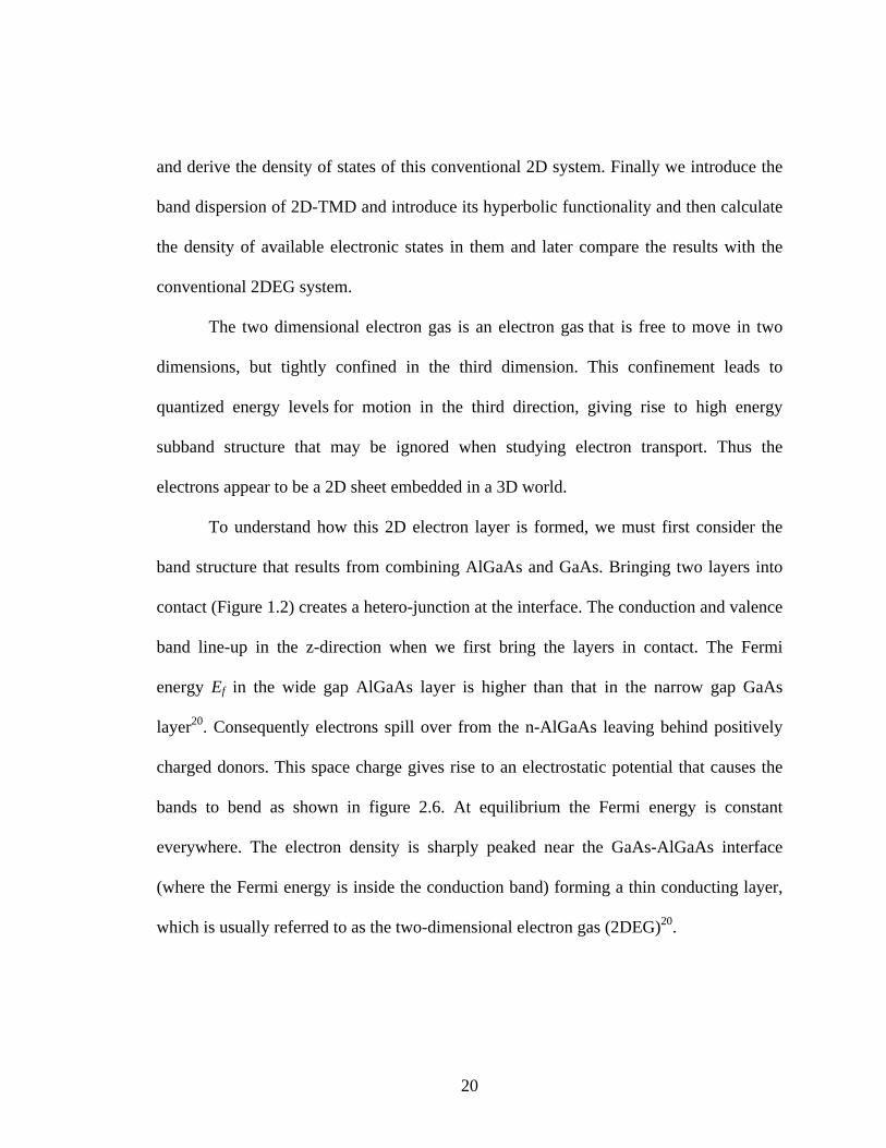
To understand how this 2D electron layer is formed, we must first consider the
band structure that results from combining AlGaAs and GaAs. Bringing two layers into
contact (Figure 1.2) creates a hetero-junction at the interface. The conduction and valence
band line-up in the z-direction when we first bring the layers in contact. The Fermi
energy Ef in the wide gap AlGaAs layer is higher than that in the narrow gap GaAs
layer20. Consequently electrons spill over from the n-AlGaAs leaving behind positively
charged donors. This space charge gives rise to an electrostatic potential that causes the
bands to bend as shown in figure 2.6. At equilibrium the Fermi energy is constant
everywhere. The electron density is sharply peaked near the GaAs-AlGaAs interface
(where the Fermi energy is inside the conduction band) forming a thin conducting layer,
which is usually referred to as the two-dimensional electron gas (2DEG)20.

21
Figure 2.6. Conduction and valence band line-up at a junction between an N-type AlGaAs ad intrinsic GaAs, a, Before and b, After charge transfer has taken place. Note that this is a cross-sectional view. This figure is adapted from reference 20.
2.4.1 Band Diagram of 2DEG
Here (in sections 2.4.1 and 2.4.2) we aim to find out the density of electronic states in a
conventional two-dimensional electron gas and study its relation with electronic energy,
then later in section 2.5 we study the density of electronic states in an atomic layer 2D-
TMD to compare the results. To calculate the density of states we need to first find out

22
the dispersion relation of the band diagram by solving the Schrodinger equation (2.3), for
a free electron gas in the absence of magnetic fields, the eigenfunctions are obtained from
equation 2.3,
ES +i!∇ + eA( )
2m
2
+U x, y( )⎡
⎣⎢⎢
⎤
⎦⎥⎥Ψ(x, y) = EΨ(x, y) (2.3)
by setting U=0 and A=0, The eigenfunctions normalized to an area S (a circle with radius
a in Fig. 2.7) have the form:
Ψ(x, y) = 1
Sexp ikxx( )exp iky y( ) (2.4)
Figure 2.7. Dispersion relation, band diagram in real space and momentum space. a, Dispersion relation for a free electron gas in two dimensions. Note that the bottom of the two-dimensional sub-band Es lies a little higher than the conduction band edge Ec in the bulk material. b, Band diagram in real space showing only the bottom of the band and the Fermi energy, Ef. c, Assuming periodic boundary conditions, kx, and ky take on quantized values depending on the dimensions of the sample. This figure is adapted from reference 20.

23
with eigenenergies given by
E = ES + !
2
2mkx
2 + ky2( ) (2.5)
The dispersion relation equation 2.5 is sketched in figure 2.7a. It is also common
to draw band diagrams in real space showing only the bottom of the band (corresponding
to kx=ky=0) and the Fermi energy.
2.4.2 Density Of States of 2DEG
Having the eigenfunctions of the dispersion relation of a 2DEG we can now
calculate the density of states. It describes the number of states per interval of energy at
each energy level available to be occupied by electrons (holes), referring to the number of
quantum states per unit energy. In other words, the density of states, denoted by g(E)
indicates how densely packed quantum states are in a particular system. Integrating the
density of the quantum states over a range of energy will produce a number of states
(N(E)) indicated by equation 2.6. The number of quantum states is important in the
determination of optical properties of a material.
( ) ( )E
EN E g E dE
Δ= ∫
(2.6)
Here g(E)dE represents the number of states between E and dE. From the Schrodinger
equation (2.4.1), we found that the energy of a particle is quantized and is given by:
E = k 2!2
2m (2.7)
The variable k is related to the physical quantity of momentum. A particle’s energy is

24
2 2 221
2 2 2m v pE mv
m m= = =
Relating the previous two equations yields
E = k 2!2
2m= p2
2m→ k = p
!
Here the momentum is a vector, which has components in the x, y, and z
directions. Therefore, k must also have direction components kx, ky, and kz. However in
2D, an electron is confined along one dimension but able to travel freely in the other two
directions. In the image below, an electron would be confined in the z-direction but
would travel freely in the XY plane and it can only exist in the well.
The wave function in a 1D well is given by
ψ (x) = Acos(kx) + Bsin(kx) (2.8)
where k = nπ
a, where a is the width of the barrier. In two dimensions:
, , and yx zx y z
nn nk k ka a a
ππ π= = =
To calculate density of states we need to find the number of states in the interval
of E and E+dE. In k-space, the interval is simply k and k+dk. In the 2D case, the unit cell
is simply a square with side length of π/a (The unit cell is the smallest shape which can
repeatedly be used to construct a lattice as in a diamond crystal). In figure 2.7c, the area
of the unit cell is:
2
0Aaπ⎛ ⎞= ⎜ ⎟⎝ ⎠

25
Next, we need to find the area of the ring and then divide by the area of the unit cell.
The area of a circle is πr2 where r is the radius. The area of the ring is then:
A = 1
4π (k + dk)2 −π k 2 = 2π kdk( )
Dividing the ring area by the unit cell area, the density of states can be found:
g(k)dk = 2 AA0
⎛
⎝⎜⎞
⎠⎟= (2)
π2
kdk
πa
⎛⎝⎜
⎞⎠⎟
2 = a2
πkdk
(2.9)
The relationship between k and E is:
k = 2mE
!2
Then:
dk = 1
22m!2
⎛⎝⎜
⎞⎠⎟
2mE!2
⎛⎝⎜
⎞⎠⎟
− 12
dE = m!2
2mE!2
⎛⎝⎜
⎞⎠⎟
− 12
dE
Substituting the results into the density of states equation (2.9) will give the density of
states in terms of energy.
g(E)dE = a2
π2mE!2
⎛⎝⎜
⎞⎠⎟
12 m!2
2mE!2
⎛⎝⎜
⎞⎠⎟
− 12⎡
⎣
⎢⎢
⎤
⎦
⎥⎥
dE
g(E)dE = a2mπ!2 dE
g(E) = a2m
π!2 (2.10)
Equation 2.10 reveals that the conventional 2D density of states, interestingly, does not
depend on energy.

26
2.5 Density of States in Transition Metal Dichalcogenides
The probability of absorbing photons depends on the number of available
electronic states. Therefore, to understand how light interacts with 2D-TMDs we need to
first understand the density of electronic states (DOS). To find out the density of
electronic states g(E) in 2D-TMD atomic layer semiconductors we use the energy
spectrum (shown in Figure 2.8) calculated theoretically through effective tight-binding
two-valley Bloch Hamiltonian21,22,23:
EτS
n k( ) = 12
λτS + n 2atk( )2+ Δ − λτS( )2⎛
⎝⎜⎞⎠⎟ (2.11)
Here, Δ is the band gap energy, 2λ is the spin splitting in the valence band, the valley
index τ=±1 corresponds to ±K points, and the spin index s=± corresponds to the z-
component of the spin. n = ±1 indexes the conduction and valence band, respectively. We
note here that the energy spectrum is hyperbolic; E(k) is approximately parabolic at low
energies but tends towards a constant linear slope at high electron energies.
The density of states in 2D-TMDs can be calculated directly from equation 2.11
and is given by:
g E( ) = 1
2nπa2t2
2E − λτSn
⎛⎝⎜
⎞⎠⎟
= 2E − λτS2n2πa2t2 (2.12)
The density of electronic states in the conduction band (n = 1) can be written as:
g E( ) = 1
πa2t2 E + EGAP( ) =EGAP
πa2t2 1+ EEGAP
⎛
⎝⎜⎞
⎠⎟ (2.13)
Here, EGAP is the energy difference between the conduction and valence band in the K

27
and K’ valleys of a monolayer TMD, such as MoSe2 or WSe2. From equation 2.13, the
density of states approaches a constant value for electrons near the bottom of the bands,
but depends linearly on the electron energy at high energies. Comparing this to equation
2.10, we note that this result is distinct from the density of states in conventional 2D
electron gases, where g(E) does not depend on energy due to parabolic band structure.
Calculating the density of available electronic states is important to understand
the electron transport through the interface of the heterostructure. Density of states being
linearly proportional to energy for this type of 2D atomic layer system forms a
completely different I-V characteristic from conventional semiconductor P-N junctions
(formulation represented in chapter 6).
Figure 2.8. Energy band diagram of a 2D-TMD material with hyperbolic band structure.

28
REFERENCES
1. Choi W., et al. Recent development of two-dimensional transition metal dichalcogenides and their applications. Materials Today, 20, 116-130 (2017).
2. Liu G. B., et al. Electronic structures and theoretical modeling of two-dimensional group-VIB transition metal dichalcogenides. Chem Soc Rev, 44, 2577-2788 (2015).
3. Zhang Y. J., et al. 2D crystals of transition metal dichalcogenide and their
iontronic functionalities. 2D Mater. 2, (2015).
4. Silva Guillen J. A. et al., Electronic Band Structure of Transition Metal Dichalcogenides from Ab Initio and Slater–Koster Tight-Binding Model. Appl. Sci. 6, 284 (2016).
5. Kresse, G. & Furthmüller, J. Efficient iterative schemes for ab initio total-energy
calculations using a plane-wave basis set. Phys. Rev. B 54, 11169-11186 (1996).
6. Kresse, G. & Hafner, J. Ab initio molecular dynamics for liquid metals. Phys. Rev. B 47, 558-561 (1993).
7. Kresse, G. & Furthmüller, J. Efficiency of ab-initio total energy calculations for
metals and semiconductors using a plane-wave basis set. Comput. Mater. Sci. 6, 15-50 (1996).
8. Blöchl, P. E. Projector augmented-wave method. Phys. Rev. B 50, 17953-17979
(1994).
9. Perdew, J. P. et al. Atoms, molecules, solids, and surfaces: Applications of the generalized gradient approximation for exchange and correlation. Phys. Rev. B 46, 6671- 6687 (1992).
10. Wang, Y. & Perdew, J. P. Correlation hole of the spin-polarized electron gas, with
exact small-wave-vector and high-density scaling. Phys. Rev. B 44, 13298-13307 (1991).
11. Kresse, G. & Joubert, D. From ultrasoft pseudopotentials to the projector
augmented- wave method. Phys. Rev. B 59, 1758-1775 (1999).

29
12. Harl, J., Schimka, L. & Kresse, G. Assessing the quality of the random phase approximation for lattice constants and atomization energies of solids. Phys. Rev. B 81, 1151261-11512618 (2010).
13. Horzum, S. et al. Phonon softening and direct to indirect band gap crossover in
strained single-layer MoSe2. Phys. Rev. B 87, 1254151-1254155 (2013).
14. Brixner, L. H. Preparation and properties of the single crystalline AB2-type selenides and tellurides of niobium, tantalum, molybdenum and tungsten. J. Inorg. Nucl. Chem. 24, 257–263(1962).
15. Bhattacharyya, S. & Singh, A. K. Semiconductor-metal transition in
semiconducting bilayer sheets of transition-metal dichalcogenides. Phys. Rev. B 86, 0754541-0754547 (2012).
16. Tongay, S. et al. Thermally driven crossover from indirect toward direct bandgap
in 2D semiconductors: MoSe2 versus MoS2. Nano Lett. 12, 5576-5580 (2012).
17. Sahin, H. et al. Anomalous Raman spectra and thickness-dependent electronic properties of WSe2. Phys. Rev. B 87, 1654091-1654096 (2013).
18. Zhang, Y. et al. Direct observation of the transition from indirect to direct
bandgap in atomically thin epitaxial MoSe2. Nat. Nanotechnol. 9, 111-115 (2014).
19. Zhang, Y. et al. Electronic structure, surface doping, and optical response in
epitaxial WSe2 thin films. Nano Lett. 16, 2485-2491 (2016).
20. Datta, S., Electron Transport in Mesoscopic Systems. (Cambridge university Press, Cambridge, 1995).
21. Sosenko, E., Zhang, J., Aji, V. Superconductivity in transition metal
dichalcogenides. arXiv 2, 1512.01261 (2016).
22. Xiao, D., Liu, G., Feng, W., Xu, X. & Yao, W. Coupled spin and valley physics in monolayers of MoS2 and other group-VI dichalcogenides. Phys. Rev. Lett. 108, 1968021-1968025 (2012).
23. Xu, X., Yao, W., Xiao, D. & Heinz, T. F. Spin and pseudospins in layered
transition metal dichalcogenides. Nat. phys. 10, 343-350 (2014).

30
CHAPTER 3
DEVICE FABRICATION & TRANSPORT MEASUREMENTS OF 2L-WSe2/MoSe2
3.1 Introduction
The devices studied in this thesis consist of two types of group-VI transition metal
dichalcogenides known as tungsten diselenide (WSe2), and molybdenum diselenide
(MoSe2). We start this chapter by carefully reviewing the wafer preparation procedure,
and then introduce the scotch and blue tape-based micromechanical exfoliation
technique. Afterwards, we explicitly illustrate the dry transfer method for assembling the
individual layers and building the van der Waals heterostructures, and finally present the
device fabrication tools and techniques.
3.2 Wafer Preparation
Two-inch Si wafers coated with 290 nm thick SiO2 with crystal planes of (100) are
used as substrates for preparing devices. We cut these wafers into small pieces with
dimensions less than 1cm x 1cm to exfoliate thin layers on them. The dimension of the
exfoliated flakes is of the order of tens of microns; so we need a way to mark the position
of them on the substrate and be able to find them easily. We pattern a mask of two
dimensional arrays that covers the whole area of the Si wafers through photolithography,
cleave the wafers, and clean them before using them for exfoliation and device
fabrication. The procedure for cleaning wafers is summarized below:

31
1. First cleaning: rinse wafer with acetone and isopropyl alcohol (IPA).
2. Spin coating photoresist: cover the surface with two layers of
hexamethyldisilazane (HDMS) and a positive resist of AZ5214.
3. Bake the wafer in 110 °C for 5 minutes.
4. Photolithography to pattern the mask on the surface of the wafer, we used Karl
Suss Mask Aligner with 1 micron resolution, we generally expose the samples for
16 seconds with ultra-violet light.
5. Develop them with a combination of one part of AZ 400K developer and four
parts of DI water for one minute and then dry them with nitrogen gas.
6. The patterned wafers then need to get etched. We use Reactive Ion Etch (RIE)
system at the Center for Nanoscale Science & Engineering with the rate of 20
µm/min for 2 minutes.
7. Lift off the resist with acetone pressure.
8. Once wafer is patterned, we then slice it into very small pieces.
9. Clean them through acetone sonication and finally rinse them in acetone and IPA.
Wafers are now ready for exfoliation, transferring and then device fabrication.
3.3 Exfoliation
We fabricated MoSe2/2L-WSe2 heterostructures by mechanical exfoliation of
WSe2 and MoSe2 flakes from bulk crystals (2D Semiconductor) onto Si wafers coated
with 290 nm-thick SiO2. There are two types of tapes that can be used for
micromechanical exfoliation of atomic layered materials, scotch tape and silicone-free

32
adhesive plastic film (blue tape). Scotch tape is good for exfoliation of graphene and
hexagonal boron nitride, for which you can take advantage of the strong adhesion of the
tape to repeat the peeling off process successively. Blue tape instead is very appropriate
for exfoliation of transition metal dichalcogenides; lower amount of adhesion is sufficient
to avoid tearing the layers apart into smaller flakes and at the same time reduce the
number of layers by peeling it off.
There are several steps for exfoliation with blue tape that makes exfoliation more
efficient:
1) Take a piece of crystal and place gently on the tape (tape #1).
2) Take another piece of tape (tape #2) and lay this tape on the tape#1 parallel,
gently press with your fingers.
3) Peel the pieces of tape off from each other, and repeat the last step over and
over to have a tape dappled with spots (unlike graphene and h-BN don’t spread it out by
exfoliating spots with flakes on top of each other, it will tear the flakes off), now you
have two pieces of tape, each of which can be used for exfoliating atomic layers of TMDs
onto SiO2/Si wafers. In general, we keep #1 for later and start using #2, the result of this
process is shown in figure 3.1a.
4) Carbon-tape the back of a Si wafer down to a clean glass slide that is also taped
down to the workstation.
5) Place tape #2 gently on Si wafer and let it adhere; do not touch the surface of

33
the tape for more adhesion.
6) These dapples will be like islands and because of their thickness there will be a
few bubbles created between them, and around this area will be tape in contact with
wafer due to adhesion, shown in figure 3.1 b, and c.
7) Exfoliate tape from wafer in such a way to have control over moving the
bubble through them, depicted in figure 3.1d.
8) Take the wafer apart from glass slide using a clean razor. In general exfoliation
methods produce flakes with different sizes and thicknesses randomly distributed over
the surface of the substrate, and only a small fraction of these flakes are atomically thin.
With this method we get at least a few monolayer, bilayer flakes at each trial. Optical
images of a few exfoliated bilayers of WSe2 and monolayers of MoSe2 are shown
respectively in figure 3.2 a and b.

34
Figure 3.1. Exfoliation process. a, Tapes #1 and #2 ready for exfoliation. b, Tweezers, blue tape and a small Si wafer carbon taped from underneath to a glass slide. c, Closer view of tape on wafer. d, Exfoliation of the tape from the wafer, showing the small angle.
Figure 3.2. Optical images of a few exfoliated layers of WSe2, and MoSe2 respectively in a and b, scale bars are 20 µm.
35
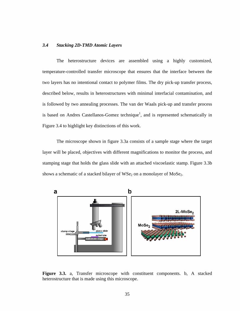
3.4 Stacking 2D-TMD Atomic Layers
The heterostructure devices are assembled using a highly customized,
temperature-controlled transfer microscope that ensures that the interface between the
two layers has no intentional contact to polymer films. The dry pick-up transfer process,
described below, results in heterostructures with minimal interfacial contamination, and
is followed by two annealing processes. The van der Waals pick-up and transfer process
is based on Andres Castellanos-Gomez technique1, and is represented schematically in
Figure 3.4 to highlight key distinctions of this work.
The microscope shown in figure 3.3a consists of a sample stage where the target
layer will be placed, objectives with different magnifications to monitor the process, and
stamping stage that holds the glass slide with an attached viscoelastic stamp. Figure 3.3b
shows a schematic of a stacked bilayer of WSe2 on a monolayer of MoSe2.
Figure 3.3. a, Transfer microscope with constituent components. b, A stacked heterostructure that is made using this microscope.

36
To achieve this, we first use a stamp to pick up the target layer, (Fig. 3.4a, top).
The stamp mounted in a micromanipulator consists of a layer of polydimethylsiloxane
(PDMS) adhered to the top of a glass slide and a thin layer of polypropylene carbonate
(PPC) spin coated on top of it. The stamp is lowered until the PPC contacts the first target
layer, WSe2. We then heat the stage to 40° C. Next, we let the stage to cool off to 34° C
and very quickly lift the stamp up, as shown in Figure 3.4b (top).
To assemble the heterostructure, we lower the WSe2 flake and place it on to the
MoSe2 flake on the stage as shown in Figure 3.4c (top). The stamp is transparent, and we
can see through it and align the orientation of the two flakes with sub-micrometer
resolution with respect to each other using the XY knobs of the translation stage on the
rotatable sample stage. The stage is then heated to 80° C, to begin melting the PPC which
then adheres strongly to the surface. The stamp is then lifted very slowly, causing the
PPC to separate from the PDMS. This leaves the stack of two flakes with PPC on top. We
then remove the residual PPC using acetone. Figure 3.4 (a, and b), bottom, show optical
images of the resultant exfoliated flakes of WSe2 and MoSe2. Dashed lines highlight the
individual layers and overlapped region of the heterostructure.
The working principle of the transfer is based on the viscoelasticity: the stamp
behaves as elastic solid at short timescales while it can slowly flow at long timescales.
Flakes are adhered to its surface because the viscoelastic material gets into close contact
with the flakes. By slowly peeling off the stamp from the surface, the viscoelastic
material detaches, releasing the flakes that adhere preferentially to the acceptor surface.

37
The stamping method can be also applied to transfer two-dimensional crystals onto pre-
fabricated devices with trenches and electrodes.
Figure 3.4. Schematic illustration and optical images of the dry-transfer process. a, b, c, (top), Schematic illustration of the transfer microscope at different temperatures for different purposes. a, b, c, (bottom), Optical images of exfoliated flakes of WSe2, MoSe2, and MoSe2/2L-WSe2 heterostructures respectively. Dashed lines indicate the area of the individual layers and the overlapped region, which are about 14µm2, 8µm2, and 4.3µm2 respectively from left to right.
3.5 Device Fabrication
Electrical contacts on the heterostructures are patterned by either electron-beam
lithography or focused ion-beam lithography and deposited by electron-beam evaporation
of Ti/Au (5nm adhesion layer /150 nm) for electrodes on each layer and on the

38
overlapped region as well. A focused beam of electrons or ions scans over the surface of
the substrate and exposes custom patterns on the electron/ion sensitive resist film
(MMA/PMMA) with ultra-high resolution.
High vacuum deposition is then used to deposit metal onto the e-beam defined
pattern. Figure 3.5a (left to right), shows several heterostructures made by transferring
flakes of figure 3.2a to b respectively. Figure 3.5b illustrates fabricated devices of figure
3.5a using EBL and E-Beam evaporation. Figure 3.6 shows optical images of the second
device from figure 3.5b in different objectives magnifications. From left to the right the
images are taken with 5x, 10x, 20x, 50x, and 100x objectives respectively.

39
Figure 3.5. a, Heterostructures made from flakes of figure 3.2 a and b. b, Heterostructures from part a with written electrodes, scale bars are 20 µm.
Figure 3.6. Optical images of a fabricated device with different magnifications from 5x
to 100x.

40
REFERENCES
1. Castellanos-Gomez, A. et al. Deterministic transfer of two-dimensional materials by all- dry viscoelastic stamping. 2D Mater. Lett. 1, 1-8 (2014).

41
CHAPTER 4
INSTRUMENTATION: LOW TEMPERATURE BROADBAND PHOTOCURRENT
SCANNING MICROSCOPE
4.1 Introduction
It was after the discovery of graphene by Andrew Geim and Noveselov that
scientists found interest in numerous other layered materials. One important family of
two-dimensional materials is the family of transition metal dichalcogenides (TMDs). In
their bulk form, TMDs have been studied for decades owing to their wide range of
electronic, optical, mechanical, chemical and thermal properties. More recently, as these
materials have been isolated into ultrathin films, optoelectronics experiment techniques
have proven great tools for exploring quantum mechanical electron and phonon behavior.
In this chapter, we discuss a novel optoelectronic probe designed to study this new family
of materials and their heterostructures.
4.2 Light-Matter Interaction at the Nanoscale
Interaction between light fields (electromagnetic radiation) and matter at the
nanoscale is a growing subject of research due to the increasing interest in the novel
phenomena that occurs as a result of this interaction. Classically, light-matter interactions
are a result of an oscillating electromagnetic field resonantly interacting with charged
particles. In the quantum view, light fields will act to couple quantum states of the matter.
As a practical basis for studying light-matter interactions, semiconductor based

42
optoelectronics is a field that has attracted a lot of attention both experimentally and
theoretically. In this chapter, we present the optoelectronic instrumentation needed to
explore quantum phenomena in nanoscale semiconductors. In later chapters, we then
present experiments that use these techniques to explore optoelectronic gain due to hot
carrier impact excitation and anti-Stokes absorption for applications in laser cooling of
TMD based semiconductor devices.
4.3 The Supercontinuum Scanning Photocurrent Spectroscopy Microscope
Supercontinuum scanning photocurrent spectroscopy microscope (SSPSM) is a
powerful tool designed to explore quantum optoelectronic properties of atomic scale
devices by integrating optics and electronics into a combined quantum transport
microscope. The SSPSM is equipped with a helium flow optical cryostat that enables
both electrical access and optical illumination to nanoscale devices through its electrical
feedthroughs and a transparent window. This cryostat can create a low-pressure
environment via a turbo pump system and can be cooled down to helium temperatures T
= 4 K.
For optical illumination a collimated beam of light is introduced to the back
aperture of an objective through optical and optomechanical components of the
microscope, generating a diffraction limited beam spot that can be scanned over the
nanoscale device. The resulting current is recorded to form a spatial map of photocurrent.
Reflected light from sample is collected by a photodiode detector (PD) converting the

43
optical power to electrical power (as a photovoltage), and the reflected intensity is
monitored to form a simultaneous image of the device.
The SSPSM microscope employs a supercontinuum Fianuim white laser as the
light source (discussed in section 4.5.1 of this chapter) along with Princeton Instrument
monochromator (see section 4.6.2 for details) for spatially and spectrally resolved
supercontinuum excitations. Power dependence experiments are achieved using
automated attenuation optics (discussed in 4.6.7).
Figure 4.1 illustrates a schematic diagram of the microscope. Laser light reaches
mirror M5 through two different paths: light either passes through the monochromator via
the left optical line in yellow, exits from its slit, hits L4 and reaches M5 for spectrally
resolved experiments, or using a flip mount mirror FM1 and a periscope (PSC) passes
through the right optical line in red and then reaches to the front of the exit slit of
monochromator. Light then reaches M5 via the second flip mount mirror (FM2) for
power dependence measurements. Laser light reflecting from M5 generates a diffraction
limited beam spot by passing through different optical components. In the following, we
give a highly detailed description of the integrated system that combines electronic and
optical tools to study nanoscale devices.

44
Figure 4.1. Schematic diagram of the supercontinuum scanning photocurrent spectroscopy microscope (SSPSM). Constituent components of the microscope comprise: light source of Fianium (LS_F), FO (fiber optics), monochromator (MC), mirrors (M), lenses (L), flip mount mirrors (FM), galvos system (GVS), beam splitter (BS), objective (OBJ), power sensor (PS), power meter (PM), photodiode detector (PD), CCD camera (CCD), cryostat (CRYO), PSC (periscope), band pass filter (BPF). Electronic experiments are conducted through the optical CRYO, while optical illumination is introduced via OBJ to devices.

45
4.4 Electronic Transport Experiment Instrumentation
A Helium flow optical cryostat is used to combine electrical measurements and
optical illumination on devices. In this section we’ll first present its application as a probe
station that enables electronic transport measurements on samples with the assistance of
several other pieces of equipment. In the next section, we describe the integration of
optical illumination to perform optoelectronic experiments.
The optical cryostat has a sample holder at the center where the sample is
mounted, surrounded by ten electrical contacts for electronic manipulation. The sample is
Figure 4.2. a, Photograph from the optical cryostat, a few BNC cables are connected to feedthroughs from right that are internally connected to the device, and two arms for vacuum pump and He transfer. b, A zoomed in view of a device in the cryostat under the microscope objective that introduces light from top to the sample, device is under vacuum.

46
separated from the outside environment by a 25.4 mm clear view epoxy sealed quartz
window for optical illumination in high vacuum. The distance between the sample holder
and the window is about 3mm, a typical working distance for many microscopic
objectives. The ten internal electrical contacts have output pin feedthroughs outside the
chamber providing electrical access to the device.
Figure 4.2a depicts a photograph from optical cryostat; the BNC cables are
connected to feedthroughs of the cryostat for electrical access to device. A zoomed in
view of the device under the microscope objective is shown in figure 4.2b. The objective
introduces a collimated laser light from top to the sample for optical illumination
presented in section 4.6.
Using a turbo pumping station, the chamber is evacuated to a pressure of 10-6
mTorr through an evacuation port located on the left arm in figure 4.2. A Si diode
temperature sensor along with a 50 Ω heater ring located at the base of the cryostat is
coupled to an external temperature controller. It can control and vary the temperature
between 4-360 K. Temperature control can be mediated also by regulating the helium
flow through He delivery line (the left arm in figure 4.2). A continuous flow of He
through the delivery line and cooling the metal base underneath the sample holder will
cool the sample to temperatures close to 4 K.
The electronic contact pads of devices on Si substrates are wire bonded to the
conductive pads (Ti/Au: 10/150 nm) of the chip carrier (a patterned substrate of sapphire)
using a wire-bonding machine. Figure 4.3a shows wire connections between device pads

47
and the chip carrier. After wire bonding, devices are soldered to the electronic pads of the
cryostat and silver painted for further electronic experiments shown in figure 4.3b.
Figure 4.3. a, Photograph of wire bonding the electrical pads of the device to contact pads of the chip carrier. b, Photograph of soldering chip carrier to electrical pins of the cryostat.
Figure 4.4. Schematics of the atomic layer device, arrangement of the layers, and the electrical contacts configuration.

48
Transport measurements are performed through the electrical configuration of the
device shown in figure 4.4, where source-drain voltage is applied to one layer and the
interlayer electrical current collected from the other while having an underneath back
gate of Si/SiO2.
All experimental parameters can be controlled though labview or a python based
software (discussed in section 4.6.6). Figure 4.5 shows a photograph of a high voltage
amplifier (Falco System WMA-100), current preamplifier (DLinstruments), switch box,
and two sets of DAQs respectively from top to bottom, with electrical connection
configuration. The two outputs of DAQ#1, labeled AO0 (in red), and AO1 (in blue)
provide input voltages for source-drain and gate respectively. A BNC cable connects
AO0 to mount #2 (top) on the switch box while mount #2 (bottom) serves as the source-
drain voltage probe used to apply voltage to one of the layers of the heterostructure.
The electrical device response must be analyzed and studied; Data Acquisition
Hardware (DAQ) supplies the input voltage and interfaces between the voltage/current
signal and the computer by converting the signal into digital values.
A grounded switch box allows physical connection between DAQ output channels
and the current/voltage probes, these probes transport electrical signal from DAQ output
channels to device and from device to computer via DAQ input channels.
In most devices, a Si/SiO2 back gate is designed to tune the carrier concentration
by electron and hole doping of the TMD heterostructures. Typically, a high voltage of up
to ±50 V is needed for the type of the heterostructures under the study of this thesis. It
can be achieved by incorporating a high voltage amplifier before the gate probe output.

49
The amplifier multiplies the signal taken from AO1 shown in figure 4.5 for the gate
voltage probe.
An Ithaco DL current preamplifier (Model 1211 with option 10) is used to convert
the electrical signal taken from the device into an output signal with a strong signal to
noise ratio by collecting the interlayer current from the heterostructure and transforming
the signal to the input channel of DAQ#2 (Ai17).
BNC cables from the cryostat feedthroughs can be plugged into the switch box
mounts labled 3-10 (bottom row), while VSD (in red), VG (in blue), and I (in purple)
probes can make the connection to device through the top row. AO2, AO3, and Ai16
connections from DAQ#2 represented in section 4.6.6.

50
Figure 4.5. Photographs and the electrical circuit diagram of the equipment used for electronic experiments.
4.5 Optical Imaging Microscopy Instrumentation
In order to conduct optoelectronic experiments on any device, it first needs to be
positioned underneath the laser excitation beam for optical illumination. Here we present
a basic optical imaging microscopy technique designed to position the devices prior to
optoelectronic experiments. A fiber optic illuminator (115 V, MI-150 fiber optic

51
illuminator w/IR Filter and Holder) with quartz halogen lamp is used as the light source
to illuminate the sample.
Figure 4.6 illustrates schematics of the optical microscope in which the divergent
beam of light source gets collimated by passing through a lens (VIS-NIR 100 mm), and
then reaches a dichroic mirror. Dichroic Mirrors/Beamsplitters spectrally separate light
by transmitting and reflecting light as a function of wavelength. Here we use a 950 nm
dichroic longpass filter, which is highly reflective below the cutoff wavelength and
highly transmissive above it. This filter reflects light shorter than 950 nm towards the
sample, and passes light longer than that emitted from the sample directly towards the
detection, so we won’t detect the scattered light caused by reflected light. The transmitted
light from dichroic mirror passes through two lenses of 75 mm and 30 mm to reduce the
image size and become compatible with the screen dimension of the CCD camera (EO-
3112C ½” CMOS Color USB Camera).
Figure 4.7a shows the schematic of the optical imaging microscope taken from
figure 4.1 and a photograph taken from the actual microscope is illustrated in part b of
figure 4.7. Fiber optics (FO) attached to a cage mount introduces light to the system.
Light reflects from mirror M11 (also coupled to the same cage mount with 45-
degree rotation) towards a lens (L8=100 mm) for collimation. Collimated light hits the
dichroic mirror (DM); it reflects wavelengths above 950 nm down to the sample after
passing through an objective (OBJ= Olympus, Plan N-10X/0.25).

52
Figure 4.6. Optical imaging microscopy, consisting of a light source, a dichroic mirror, image reducer (a pair lens), an objective, and a CCD camera.
Figure 4.7. a, Schematic of the imaging microscope. b, Optical diagram on a photo of the actual microscope. c, An optical image taken with this optical microscope from a device.

53
Light in higher wavelengths is then back reflected from sample, passes through
DM, and hits the second mirror (M12). The reflected light from M12 passes through two
lenses (L10=75 mm, and L11=30 mm) to reduce the image size and eventually reaches a
CCD camera that is connected to PC for imaging. Figure 4.7c shows an optical image of
a device taken with this microscope.
4.6 Optoelectronic Experiment Instrumentation
Optoelectronic experiments are performed by combining optical illumination
along with electronic measurements on the devices mounted in the cryostat.
Supercontinuum scanning photocurrent spectroscopy microscope (SSPSM) uses a
broadband supercontinuum white laser for the light source, which makes it a unique and
powerful experimental technique to investigate spatially and spectrally resolved
optoelectronic properties of nanoelectronic devices. In this section we present
supercontinuum scanning photocurrent spectroscopy microscope (SSPSM) by dissecting
it into its constituent components and explaining each part separately before discussing
the assembly of a combined microscope for spatially and spectrally resolved
measurements.
4.6.1 Fianium Supercontinuum Ultrafast Fiber Lasers
One of the major components of every optical microscope is the light source; a
Fianium supercontinuum is the light source coupled to this microscope for spatially and

54
spectrally resolved excitations. In optics, a supercontinuum is formed when a collection
of nonlinear processes act together upon a pump beam in order to cause severe spectral
Figure 4.8. a, A typical supercontinuum spectrum in red and the pump pulse in blue, this panel is adapted from reference 2. b, Power dependence supercontinuum spectra of Fianium SC400-8.
broadening of the original pump beam, for instance using a microstructured optical fiber1.
The result is a smooth spectral continuum.
Figure 4.8a shows a typical supercontinuum spectrum. The blue line shows the
spectrum of the pump source launched into a photonic crystal fiber while the red line
shows the resulting supercontinuum spectrum generated after propagating through the
fiber. The output of these lasers consists of just one wavelength with a combination of
these desirable features: high output power, broad and flat spectrum, very broad spectral
bandwidth, high degree of spatial coherence that allows tight focusing and the
corresponding low temporal coherence, generating ultrafast broadband supercontinuum
light2.

55
The light source we use for this microscope is a Fianium WhiteLaseTM SC400-8; a
picosecond pulsed laser pump (repetition rate = 20 MHz, pulse width = 6 ps) is launched
into a micro-structured optical fiber (the non-linear medium) of 1.5-meter length. At the
output of the fiber, the collimated white beam of light has an average power of 8 W and a
power spectral density of 4 mW/nm that ranges from λ ~ 400-2200 nm, yielding a
resolving power of about 3W in the visible range. The Fianium supercontinuum spectrum
used for this microscope is shown in figure 4.8b, the pump source is at 1055 nm, as
shown from the sharpest peak in the spectrum.
4.6.2 Princeton Instruments Monochromator
In order to spectrally resolve the supercontinuum light, we use Princeton
Instruments monochromator (SP-2300). Incoming light at the entrance slit of the
monochromator is directly imaged to the exit slit after passing through a diffraction
grating (DG1). Figure 4.9 shows schematics of the optical diagram of laser light that
passes through different components of the monochromator of the microscope.
There are two micrometer-controlled slits implemented in the monochromator
(MC) to adjust their width from 10 µm to 3 mm. These are rectangular apertures through
which light enters into and exits from the MC. They control the spectral resolution of the
MC by separating close wavelengths.
Light is focused onto the entrance slit and reflected by the first mirror (M1) onto
the parabolic collimating mirror (CM). The collimating mirror collimates the light and
reflects it directly to the diffraction grating (DG1) in this image. SP-2300 has a triple

56
grating turret labeled DG1, DG2, and DG3 shown in figure 4.9. Each of them has a
specific number of gratings 600, 300, and 150 g/mm respectively with identical blazing
wavelength of 1.2 µm. The blaze wavelength is the wavelength for which the blazed
grating is most efficient. Diffraction grating disperses the light and spatially separates it
into constituent spectral components. In figure 4.9 three colors of purple, green, and red
are indicative of diffracted light.
After the diffraction grating, light is re-focused by parabolic focusing mirror (FM)
onto the exit slit. Only the particular wavelength that falls directly on the exit slit passes
through it and is detected (in diagram of figure 4.9 white light enters the MC and only
green passes through the exit slit).
A motorized controller adjusts the angle of the diffraction grating to align the
spectrally separated light components towards the exit slit. The width of the exit slit
should be adjusted to narrow the output spectral distribution. This controller operates
through the Acton Monochromator Control software on a PC. The functions on the
software allow changing the gratings, the wavelength, wavelength scanning and the rate
of scan, shown in figure 4.10a. Diffraction grating efficiency curves of SP-2300 as a
function of wavelength for DG1, DG2, and DG3 respectively are shown in Figure 4.10b.
Since the blazing wavelength of our MC is 1.2 µm, the response signal exists between
yellow (800 nm-blaze), and red (2 µm-blaze) curves.

57
Figure 4.9. Schematics of the ray diagram of SP-2300 monochromator.
Figure 4.10, a. Monochromator Control Software, b. Grating efficiency curves of SP2300.

58
4.6.3 Getting Light Into A Monochromator
To achieve the highest optical throughput, we aim to get as much light into the
monochromator as possible, regardless of geometry. Each monochromator has an
acceptance pyramid, often described by an F/# or numerical aperture (NA). It’s a measure
of energy throughput, lower F/# means better light gathering power and energy
throughput. The position and dimensions of the internal optics determines this pyramid.
Usually the pyramid is treated as an acceptance cone with the cone peak on the center of
the entrance slit, and the F/# defined by an equivalent circle on the square grating image3.
In order to reach the maximum achievable performance in coupling a point source
laser to a monochromator, we need to collect as much light as possible from the source
and focus it on the entrance slit opening at an F/#, which is equal to the monochromator
F/#. There are two rules for most efficient coupling; First, we fill the monochromator
acceptance cone by choosing a correct F/#. Second, get as much light as possible through
the slit while observing the first guideline. The numerical aperture of the lenses we
choose to focus light into the entrance slit matches the effective numerical aperture of the
monochromator lens system (SP-2300) with f/3.9.
Figure 4.11 shows a diagram of the lens system required to introduce light into
the MC. The output of the fiber optics is a collimated beam of white light with diameter
of 𝑑!= 3 mm. To fill the acceptance cone we need to first expand the laser beam, at least
two lenses (L1, and L2) are necessary to accomplish this. In figure 4.11 the laser beam of
diameter 𝑑!is expanded to 𝑑!using a concave lens with focal length -f1 and a convex lens

59
with f2.
The numerical aperture of L3 should match the numerical aperture of MC, which
gives us 𝐹#!" = 3.9 𝑚𝑚 = !!!!
(I), for a collimated light 𝑑! = 𝑑!. The expansion ratio
gives 𝑑! =!!!!
𝑑! =!!!!
×3 𝑚𝑚 (II); plugging (I) into (II) defines the relation (III)
between the focal length of these three lenses to get the most efficiency out of the SP-
2300 MC. 𝑑! =!!!!
×3 mm = !!!.! !!
, or !!!!.!
= !!!!
(III).
The lenses we choose should apply in equation III, and be compatible with the
optical elements of the MC. The lenses used in this microscope are inked VIS-NIR
achromatic lenses with f1 = -50 mm, f2 = 200 mm, and f3 = 50mm, designed to limit the
effects of chromatic and spherical aberration. Inked lenses minimize the stray light within
an optical system, while achromatic lenses are corrected to bring two wavelengths
(typically red and blue) into focus on the same plane.
Figure 4.12 a, and b show the schematic diagram and photograph of the optical
and optomechanical components of the microscope to get light into the monochromator.
Light beam coming with diameter of 3mm from the Fianium laser source (LS_F) reflects
from first mirror (M1) into a right-angled mirror (M2) that reflects light upward to a
height equal to the center of the entrance slit of the monochromator.

60
Figure 4.11. Diagram of the lens system required for getting light into the entrance slit of MC.
Figure 4.12. Getting light into the MC. a, Schematics of the optics that introduces light into the MC. b, Optical diagram on a photograph of the actual microscope to introduce light to the MC.
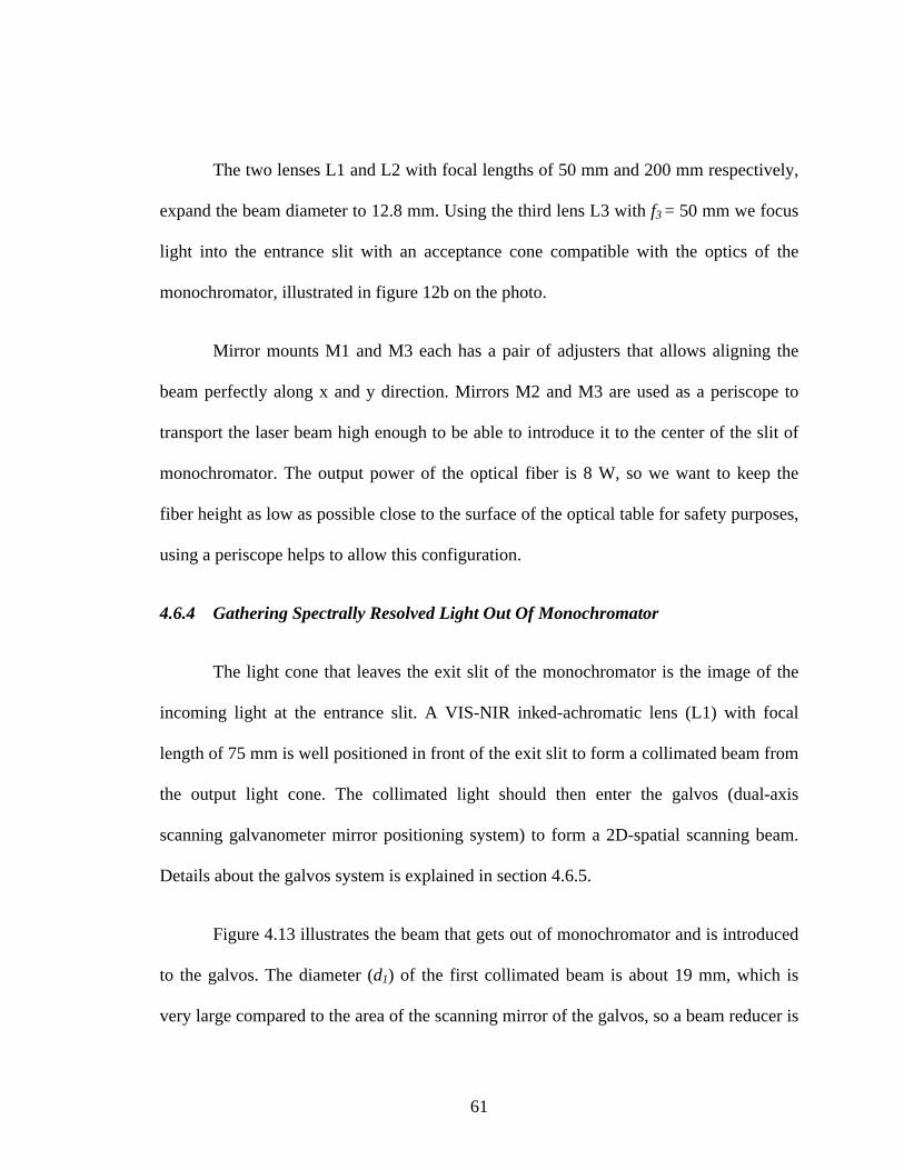
61
The two lenses L1 and L2 with focal lengths of 50 mm and 200 mm respectively,
expand the beam diameter to 12.8 mm. Using the third lens L3 with f3 = 50 mm we focus
light into the entrance slit with an acceptance cone compatible with the optics of the
monochromator, illustrated in figure 12b on the photo.
Mirror mounts M1 and M3 each has a pair of adjusters that allows aligning the
beam perfectly along x and y direction. Mirrors M2 and M3 are used as a periscope to
transport the laser beam high enough to be able to introduce it to the center of the slit of
monochromator. The output power of the optical fiber is 8 W, so we want to keep the
fiber height as low as possible close to the surface of the optical table for safety purposes,
using a periscope helps to allow this configuration.
4.6.4 Gathering Spectrally Resolved Light Out Of Monochromator
The light cone that leaves the exit slit of the monochromator is the image of the
incoming light at the entrance slit. A VIS-NIR inked-achromatic lens (L1) with focal
length of 75 mm is well positioned in front of the exit slit to form a collimated beam from
the output light cone. The collimated light should then enter the galvos (dual-axis
scanning galvanometer mirror positioning system) to form a 2D-spatial scanning beam.
Details about the galvos system is explained in section 4.6.5.
Figure 4.13 illustrates the beam that gets out of monochromator and is introduced
to the galvos. The diameter (d1) of the first collimated beam is about 19 mm, which is
very large compared to the area of the scanning mirror of the galvos, so a beam reducer is
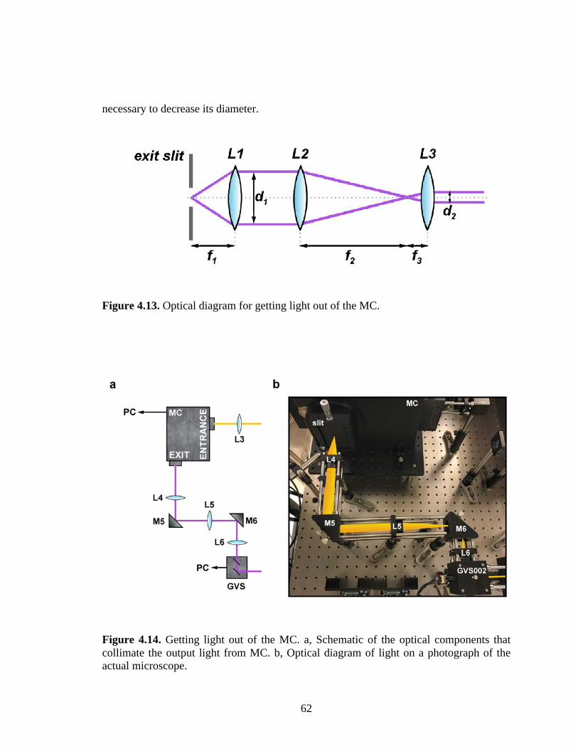
62
necessary to decrease its diameter.
Figure 4.13. Optical diagram for getting light out of the MC.
Figure 4.14. Getting light out of the MC. a, Schematic of the optical components that collimate the output light from MC. b, Optical diagram of light on a photograph of the actual microscope.
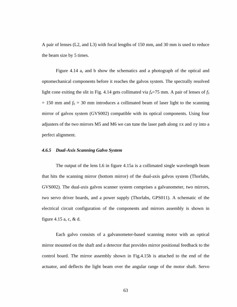
63
A pair of lenses (L2, and L3) with focal lengths of 150 mm, and 30 mm is used to reduce
the beam size by 5 times.
Figure 4.14 a, and b show the schematics and a photograph of the optical and
optomechanical components before it reaches the galvos system. The spectrally resolved
light cone exiting the slit in Fig. 4.14 gets collimated via f4=75 mm. A pair of lenses of f5
= 150 mm and f6 = 30 mm introduces a collimated beam of laser light to the scanning
mirror of galvos system (GVS002) compatible with its optical components. Using four
adjusters of the two mirrors M5 and M6 we can tune the laser path along ±x and ±y into a
perfect alignment.
4.6.5 Dual-Axis Scanning Galvo System
The output of the lens L6 in figure 4.15a is a collimated single wavelength beam
that hits the scanning mirror (bottom mirror) of the dual-axis galvos system (Thorlabs,
GVS002). The dual-axis galvos scanner system comprises a galvanometer, two mirrors,
two servo driver boards, and a power supply (Thorlabs, GPS011). A schematic of the
electrical circuit configuration of the components and mirrors assembly is shown in
figure 4.15 a, c, & d.
Each galvo consists of a galvanometer-based scanning motor with an optical
mirror mounted on the shaft and a detector that provides mirror positional feedback to the
control board. The mirror assembly shown in Fig.4.15b is attached to the end of the
actuator, and deflects the light beam over the angular range of the motor shaft. Servo

64
driver boards displayed in Fig. 4.15c interpret the signal from the optical position
detecting system inside the motor and then produce the drive voltage required to rotate
the mirror to the desired position. The galvo power supply shown in Fig. 4.15 d allows
two driver cards to be powered via the separate 2 m power cables.
The two output channels of DAQ#2 (A02, and AO3) illustrated in figure 4.5
provide DC voltages required for the actuator attached to the mirrors through LabView
control or the custom-written python based software (SSM). Connections from DAQ
output channels (AO2 and AO3) to driver boards are colored in yellow and from power
supply to x-scanning and y-scanning driver boards and eventually to the actual actuators
in cyan and pink respectively.
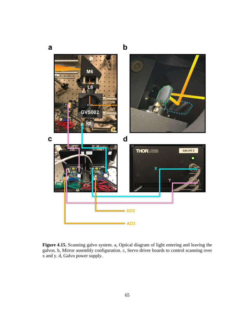
65
Figure 4.15. Scanning galvo system. a, Optical diagram of light entering and leaving the galvos. b, Mirror assembly configuration. c, Servo driver boards to control scanning over x and y. d, Galvo power supply.

66
4.6.6 Spatially And Spectrally Resolved Laser Excitations
The beam reflecting from the scanning mirror propagates into a pair of inked
achromatic lenses before entering the microscope. In order to maximize the optical power
focused onto the device the laser beam should fill the rear aperture of the microscope
objective. The diameter of the beam leaving the scanning mirror is about 4 mm (about the
size of the aperture) therefore the focal length of these two lenses are chosen equal
f1=f2=100 mm to avoid beam expansion or reduction. Their only function is to translate
the image from the scanning mirror to the rear aperture of the microscope.
Choosing inked achromatic lenses allow the laser beam scanning on the surface of
the device without aberration and stray light. Figure 4.16 shows a schematic of the light
propagation from scanning mirror (M1) towards the aperture and then scanning over
device surface.
Figure 4.16. Schematics of the scanning Gaussian beam over the surface of the sample.

67
Scanning mirror M1 reflects the collimated light to mirror M2 from which it’s
introduced into the lens pair L1 and L2. The lens pair images the beam spot at M1 to the
spot at the back of the objective (OBJ) of the microscope via a beam splitter (BS) that
reflects 90% of light towards the sample. The light is then focused to a diffraction-limited
spot on the surface of the sample in the cryostat using the objective.
Since the two lenses L1 and L2 have equal focal lengths the spot size remains
consistent. The beam that passes through the center of the lenses with no deflection is
shown in purple in Fig 4.16. When the scanning mirror rotates, the collimated beam is
deflected from center; two angles of scanning are illustrated in figure 4.16 by red, and
green. With a deflected light the image still forms on the same spot at the rear of the
objective but with an angle of incidence. The actuating voltage applied to the
galvanometer from the output channels (AO2, and AO3) can controllably change the
angle of incidence and scan the focused Gaussian beam across the sample surface and
generate a spatial map of photogenerated current.
The reflected light from sample transmits through the BS and reflects to a lens
(L3) with focal length of f3 = 50 mm via a right-angled mirror (M3), and finally gets
collected by a photodiode detector (PD). The photodiode converts the optical power to
electrical power as a photovoltage; the intensity of the photovoltage is monitored to form
a simultaneous reflection image of the sample.
To monitor the whole wavelength range we use two photodetectors. A Si
switchable gain detector (Thorlabs: PDA36A) is sensitive to the light from UV to NIR

68
wavelength range (350-1100 nm), and an InGaAs photodetector (Thorlabs: DET10C) on
the other hand is designed to detect light signals ranging from 900 to 1700 nm. The light
beams reflecting back from sample surface get focused on the screen of PD to form
simultaneous reflection image of the sample, from which differential reflection analysis
would be possible. Figure 4.17a,b shows the schematics and actual optomechanical
components of the microscope that introduces light from galvos (GVS) to the objective
and eventually to the sample for 2D scanning.
As mentioned in section 4.6.1 of this chapter, the Fianium light source provides
white light in a broad spectral variance between 400-2200 nm. To achieve the highest
performance of this microscope over such a broad spectral range, optical components
should match the wavelength range that we choose to conduct experiments. There are
three different beam splitter coatings to cover the whole wavelength range. Thorlabs non-
polarizing achromatic beam splitter cubes can provide a uniform reflection in these three
ranges; BS028 for Vis (400-700 nm), BS029 for NIR (700-1100 nm), and BS030 for IR
(100-1600 nm).
The objective used for this microscope is an Olympus UCPLAN N 50X with a
high numerical aperture of 0.65 and a long working distance of 2-4 mm. It’s designed for
optimal transmission in the near infrared (700-130 0nm wavelengths). Using this
objective at the wavelengths beyond this range would cause a slight power loss. To have
a high efficiency microscope we can mate the BS and OBJ depending upon a change in
the wavelength range. These objectives include a corrector ring that adjusts internal

69
optics to focus through the glass medium; it’s designed to compensate for the optical
aberrations caused by focusing light through a 1 mm thick transparent glass window of
the cryostat.
Figure 4.17. Diffraction limited beam spot to the cryostat. a, Schematics of the optics to introduce light to sample. b, Optical diagram on a photograph of the actual microscope.

70
As mentioned earlier in this section these beam splitters reflect 90% of the light to
the sample; the 10% of the light that transmits through the BS can get detected with a
power sensor (PS) coupled to a power meter (PM). The power sensor response function
should also match the wavelength range of the microscope; using two power sensors
(Thorlabs: S130C, and S132C) we can accurately detect the optical power in the ranges
of 400-1100 nm and 700-11800 nm respectively in the power range of 500 pW-500 mW.
In this scanning photocurrent microscopy technique the reflected light and the
device current are simultaneously collected as the focused laser spot is scanned across the
surface of the sample and as a result a pair of correlated spatial maps are generated.
These maps are then displayed and analyzed using LabView or python custom-written
control software.
Through this microscope we can perform spatial imaging as a function of
wavelength by fixing the spectrum at a specific wavelength and conducting 2D spatial
scans over the surface of the sample, as changing other parameters such as VSD, VG, or
temperature in order to make 3D or 4D data cubes. We can also perform spectral imaging
with a narrow resolution of 1 nm by fixing the laser beam at a specific spot on the device
(preferably the heterostructure) while tuning the spectral range over y axis, in this case x
axis could be variation of other parameters such as VSD, VG, or temperature.
4.6.7 Power Dependence Experiments
Another unique function of the supercontinuum scanning photocurrent

71
spectroscopy microscope (SSPSM) is the ability of allowing power dependence scanning
experiments at any specific wavelength within the range of 400-2200 nm. The fiber
output power is 8 W, which is high enough for generating a power dependence
experiment.
In figure 4.18a placing a mirror on a flip mount (FM1) allows us to deflect laser
light from reaching M2. The white light with 8W power then reflects into a periscope and
from there reaches a band-pass filter. Using Thorlabs band-pass filters we can allow a
specific wavelength with only ± 2 nm to transmit through and reach M9. These filters cut
out the laser power to tens of mW, which is pretty good for power dependence
experiments. Using the second flip mount (FM2) we lead the light towards reaching the
galvo system to again generate a diffraction limited beam spot.
Figure 4.18. Power dependence experiment. a, Schematic of the supercontinuum scanning photocurrent spectroscopy microscope (for a more clear image please see Fig. 4.1). b, Leading optical light from source to a band pass filter (BPF) using a flip mount (FM1). c, Optical light path from BPF to FM2.

72
Placing a motorized rotation mount (Thorlabs, K10CR1) coupled to a
continuously variable reflective neutral density filter (Thorlabs, NDC-50C2) in front of
the laser light allows us to control the intensity of the power. These filters provide linear,
adjustable attenuation within the coated region via rotation. Using this function of the
microscope we can spatially scan surface of devices while stepping through the new
parameter, which is optical power. Figure 4.18b, and c illustrate ray diagram on the
photographs taken from the actual microscope.
4.7 Running Experiments Through Software
Photocurrent and reflected photovoltage VREF from spatial or spectral scanning
can be imaged simultaneously while running the experiments. Using LabView or SSM (a
custom-written python based software) helps us to vary different input parameters and get
a view of the outcome signal in maps.
Figure 4.19a shows a profile of SSM software, consisting of three main panels at
the left to vary and control parameters. Panel_1 allows us to center the reflection imaging
or the photoresponse on the maps, set a fixed value for source-drain and gate voltages,
vary number of pixels along X and Y axis as well as changing the scan line rate. Through
panel_2 we can assign back-gate (AO1), source-drain (AO0), or x-axis (AO2) as the fast
scanning axis along x direction, whereas assign back-gate (AO1), source-drain (AO0),
Wavelength, or y-axis (AO3) along y direction as the slow scanning axis within a desired
range. Panel_3 allows generating data cubes of 2D spatial scans with the third parameter
being change in one of parameters of back-gate, source-drain or wavelength, as well as

73
repeating the data cube in another direction to generate 4D scans by varying one of the
other two remaining parameters.
Right column on the software profile shows 2D maps of reflection image and
photocurrent image taken from device in panel b of this figure, photoresponse is observed
where there is an overlap between the two layers of the heterostructure.
Figure 4.19. Profile of the custom-written SSM software. b, Optical image of a device consisting a 2L-WSe2 stacked on top of a 1L-MoSe2.

74
REFERENCES
1. NKT Photonics, www.NKTPhotonics.com 2. Robert R. Alfano, The Supercontinuum Laser Source, The ultimate white light.
Library of congress, New York, (2016).
3. Eugene Hecht, Optics, Fifth edition. Pearson Education, (2017).

75
CHAPTER 5
BASIC OPTICAL CHARACTERIZATION OF TMD HETEROSTRUCTURES
5.1 Introduction
The investigations of optical properties of layered materials represent one of the
main directions of current materials research, as light exposes many of the properties of
semiconductors and their structures. There exist many techniques to explore optical
properties of materials, among which Raman and photoluminescence are two that are
widely used in research and materials development. Raman spectroscopy is a
spectroscopic technique used to observe vibrational, rotational, and other low frequency
modes in a system. Because the vibrational spectrum is sensitive to the sample thickness,
Raman spectroscopy has been widely used to determine the number of layers of
exfoliated transition metal dichalcogenides; the energy, width, and amplitude of the
vibrational modes are strongly influenced by the thickness of the flakes. These
vibrational modes of the crystalline lattices are called phonons. On the other hand,
Photoluminescence (PL) is the light emission from any form of matter after the
absorption of photons. In this chapter we first present a comprehensive optical
characterization of transition metal dichalcogenides - MoSe2, WSe2 and heterostructures
composed of these materials - via two powerful optical spectroscopy techniques: Raman
and Photoluminescence. Using extensive characterization including differential
reflection, and photocurrent spectroscopy, we confirm strong interlayer electronic
coupling at the heterostructure interface. Photocurrent spectroscopy measurements, which

76
expose a great deal of new information about the heterostrucutres examined here, are
presented in chapters 5 and 6 in high detail.
5.2 Raman Spectroscopy
Raman Spectroscopy is a non-destructive analysis technique that provides
detailed information about the chemical structure, crystal structure, and molecular
interactions. Raman spectroscopy is based on the interaction of light with the chemical
bonds within a material, and directly probes the lattice vibrations of a crystal. To model
the vibrational modes of a molecule or crystal, we assume that the material is composed
of masses (atoms) joined by springs (chemical bonds), so that an input of energy into the
system will lead to mechanical vibrations. Each of these vibrational modes is initiated by
a specific frequency, usually in the infrared region of the electromagnetic spectrum, and
in many systems they are quantized like electronic energy levels. These molecular
vibrations cause a change in the polarizability or the dipole moment of the molecules.
When a high intensity laser light is introduced to a material, the molecules scatter the
incident light. A small fraction of scattered light emerges at different wavelength from
the initial light source, and the energy difference depends on the structure of the material.
This process, called Raman scattering1 may occur through the absorption or emission of a
phonon within the crystal structure.

77
Figure 5.1. Schematic drawing of the four Raman active and two inactive modes of the transition metal dichalcogenides MX2 (M=Mo, W and X=Se, S). This figure is adapted from reference 1.
We use Raman spectroscopy to determine the number of layers of exfoliated
transition metal dichalcogenides as the energy, width and amplitude of the vibrational
modes are strongly influenced by the thickness of the flakes and also to identify the
vibrational Raman active modes in the atomic layers.
There are four Raman active and two inactive modes of the transition metal
dichalcogenides MX2 (M = Mo, W and X = Se, S) representing different vibrations of the
atoms in the lattice, shown in figure 5.1. Raman active mode consists of three in-plane
modes (E1g, E12g, and E2
2g) and one out of plane mode (A1g).
The devices, shown in Figure 5.2 a & d, were first characterized to identify layer
thickness and ensure interlayer coupling, as determined through Raman and
photoluminescence (PL) spectroscopy. We used a Horiba LabRAM HR spectrometer
with an excitation of 532 nm, with working range of 100 cm-1 to 9700 cm-1.

78
Measurements are performed at room temperature with the power of excitation laser at 2
mw for both individual layers of MoSe2 and WSe2 and the overlapped region of the
heterostructures WSe2/MoSe2. Figure 5.2 b & e show the Raman spectrum for the MoSe2
and WSe2 flakes that were carried out before and after constructing the heterostructure.
For the monolayer MoSe2 we observed a very active mode at 241 cm-1 (30 meV),
and another mode at 289 cm-1 (36 meV). The first Raman active vibrational mode is
assigned to an out of plane vibration of Aˊ in which Se atoms oscillate in opposite phase
perpendicular to the atomic plane with respect to Mo atom at the center not moving, while
the second not very active mode to an in-plane vibration of E12g, at each unit cell this low
intensity mode is caused by Se atoms oscillating in opposite phase with Mo atom in the
plane of the atomic layer. Our measurements are in excellent agreement with other
studies attributing these vibrations to a monolayer Mose2.
For bilayer WSe2 we found a very active Raman mode at 250 cm-1 (31 meV), and
two other modes one at 256 cm-1 (31.7 meV) and the other at 308 cm-1 (38 meV). Based
on many previously reported literatures the combination of these modes is an indication
of having a bilayer material. The first two very close modes near 30 meV are assigned to
E12g and A1g respectively. In E1
2g vibrational mode two in phase Se atoms oscillate in
opposite to a W atom at each layer and the two layers oscillate laterally opposite to one
another, while in A1g mode Se atoms oscillate in opposite phase, out of plane with respect
to W atoms.

79
Figure. 5.2. Optical images, Raman spectroscopy, and PL spectroscopy of Devices 1 and 2. a, d, Optical images of the two MoSe2/2L-WSe2 heterostructures with contacts. b, e, Raman spectra (excitation wavelength λ=532 nm) for MoSe2 (green), and 2L-Wse2 (blue). c, f, PL spectra of MoSe2 (green), 2L-WSe2 (blue), and the stack (black).

80
5.3 Photoluminescence Spectroscopy
Figure 5.2 c & f show the room temperature photoluminescence (PL) spectra with
a laser wavelength λ= 532 nm fixed on the individual TMDs and on the overlapped
region. A schematic of the device geometry along with higher resolution PL spectra taken
from each layer and the overlapped region is shown in figure 5.3 a and b respectively. In
the monolayer MoSe2 (green line, Fig. 5.3 b), PL peaks were observed at photon energy
EPH = 1.57 eV and 1.75 eV, while in 2L-WSe2 (blue line, Fig. 5.3 b), two peaks were
observed at EPH = 1.46 eV and 1.66 eV. When measured in the heterostructure overlap
region, we observed strong suppression of the lowest energy PL peak (originating from
the WSe2), and an order of magnitude decrease of the PL peaks at 1.55 eV and 1.64 eV.
Such PL suppression, which was typical of these devices, has been studied previously2-6
and is attributed to charge redistribution and the formation of spatially indirect, bound e-h
pairs at the interface.
The PL spectra of the heterostructure devices show several key features that indicate
interlayer electron transfer and equilibrium charge redistribution between the layers in the
heterostructure7,8. Figure 5.2c shows the photoluminescence (PL) spectra of MoSe2, 2L-
WSe2, and the heterostructure. The PL emission of MoSe2 has a large peak at 1.57 eV
and a shoulder at 1.75 eV, while the 2L-WSe2 exhibits two peaks at 1.46 eV and 1.66 eV,
in agreement with previously reported data2. Figure 5.2 (d, e, and f) shows
characterization data for a second 2L-WSe2/MoSe2 heterostructure, Device 2. Raman
spectra and PL are again in agreement with the results of ref1.

81
Figure 5.3. Device geometry and the PL spectra of the 2D semiconductor heterostructure device. a, Schematics of the atomic layer heterostructure. b, Photoluminescence (λ = 532 nm) from MoSe2 (green), 2L-WSe2 (blue), and the heterostructure (black).
5.4 Photocurrent and Differential Reflection Spectroscopy
After devices were placed into high vacuum (10-6 torr), we first annealed the
samples at 420 °C for 48 hours to improve device contact quality and remove surface
contaminants6. Following this procedure, the devices were kept under a 10-6 torr vacuum
at all times. We carried out scanning photocurrent spectroscopy measurements using a
tunable Ti:sapph laser with 200 fs pulse duration and a 76 MHz rep rate combined with a
custom-built scanning microscope9. The photocurrent was measured with a diffraction-
limited beam spot at various wavelengths over the Ti:sapph laser range (wavelengths
700-1000 nm) and at average powers below 1 mW. After initial photocurrent
measurements to assess device contacts, the device resistance and DC current noise was
significantly decreased when measured at low and high VSD voltage. An order of

82
magnitude decrease in the low-bias (VSD < 0.5 V) resistance was typical after 12-24
hours of sustained scanning photocurrent measurements under vacuum, after which time
the device remained stable. Each of the devices described here were measured for more
than 60 days, and demonstrated stable operation after annealing.
After annealing, photocurrent and differential reflection spectra were taken to
confirm interlayer coupling at the interface, as determined by the strong correlation with
PL spectral features. We measured photocurrent and reflection spectra with a 0.7 mW
beam focused to a diffraction-limited 500 nm diameter (FWHM) spot. Figure 5.4 a shows
photocurrent (red), ΔR/R (blue), and PL (gray) as a function of incident photon energy.
The quantity ΔR/R is the difference between the reflection at any point and the reflection
of the silicon substrate, normalized by the background reflection from the substrate. In
Figure 5.4 b we show spatial ΔR/R maps taken at different wavelengths. We observed a
clear spatial dependence of ΔR/R, and a wavelength-dependent transition from positive,
through zero, and then to negative ΔR/R. We took the data from the green dot in Figure
5.4 b to plot the ΔR/R spectrum in Figure 5.4 a. The zero crossing of the ΔR/R spectrum
occurs near 1.45 eV, and a minimum in ΔR/R occurs at 1.66 eV, slightly higher in energy
than the peak in PL emission. The photocurrent shows a peak near 1.66 eV and continues
to increase at higher photon energies.

83
Figure. 5.4. Differential reflection and photocurrent spectroscopy measurements of Device 1 in figure 5.2. a, Photocurrent, ΔR/R, and PL spectra from MoSe2/2L-WSe2 heterostructure illustrated respectively by red, blue, and gray lines. b, Spatial ΔR/R maps at different excitation photon energies (labeled).

84
REFERENCES
1. Tonndorf Ph., et al., Photoluminescence emission and Raman response of monolayer MoS2, MoSe2, and WSe2. OPTICS EXPRESS 4909, 21 (2013).
2. Hong, X. et al. Ultrafast charge transfer in atomically thin MoS2/WS2
heterostructures. Nat. Nanotechnol. 9, 682-686 (2014).
3. Rivera, P. et al. Valley-polarized exciton dynamics in a 2D semiconductor heterostructure. Nat. Commun. 6, 1-6 (2015).
4. Rivera, P. et al. Observation of long-lived interlayer excitons in monolayer
MoSe2– WSe2 heterostructures. Science 351, 688-691 (2016).
5. Rigosi, A. F., Hill, H. M., Li, Y., Chernikov, A. & Heinz, T. F. Probing Interlayer Interactions in Transition Metal Dichalcogenide Heterostructures by Optical Spectroscopy: MoS2/WS2 and MoSe2/WSe2. Nano Lett. 15, 5033-5038 (2015).
6. Furchi, M. M., Pospischil, A. A., Libisch, F., Burgdörfer, J. & Mueller, T. Photovoltaic Effect in an Electrically Tunable van der Waals Heterojunction. Nano Lett. 14, 4785- 4791 (2014).
7. Rivera, P. et al. Valley-polarized exciton dynamics in a 2D semiconductor
heterostructure. Nat. Commun. 6, 1-6 (2015).
8. Ceballos, F., Bellus, M. Z., Chiu, H. & Zhao, H. Ultrafast charge separation and indirect exciton formation in a MoS2–MoSe2 van der waals heterostructure. ACS Nano 8, 12717- 12724 (2014).
9. Kresse, G. & Furthmüller, J. Efficient iterative schemes for ab initio total-energy
calculations using a plane-wave basis set. Phys. Rev. B 54, 11169-11186 (1996).

85
CHAPTER 6
HOT CARRIER-ENHANCED INTERLAYER ELECTRON-HOLE PAIR
MULTIPLICATION In VDW HETEROSTRUCTURE PHOTOCELLS
6.1 Introduction
Two-dimensional TMDs have captured a great deal of attention in the scientific
communities for their wide range of unique properties, as well as their promise for
electronic and optoelectronic performance at the nanoscale. In this chapter, we describe
the electronic operation and electronic transport measurements of heterostructures
composed of WSe2 and MoSe2. We measure the electronic transport characteristics at
various regimes of applied bias and gate voltage as a function of temperature. Through
interlayer I-VSD characteristics we report on highly efficient multiplication of interlayer e-
h pairs in these 2D semiconductor heterostructure photocells, indicating that layer-
indirect e-h pairs are generated by hot electron impact excitation at temperatures near T =
300 K. By exploiting this highly efficient interlayer e-h pair multiplication process, we
demonstrate near-infrared optoelectronic devices that exhibit 350% enhancement of the
optoelectronic responsivity at microwatt power levels. Our findings, which demonstrate
the remarkable efficiency of carrier multiplication in TMD- based optoelectronic devices,
make 2D semiconductor heterostructures viable for a new class of ultra-efficient
photodetectors based on layer-indirect electron-hole excitations. The main results of this
chapter were published in reference 1.

86
6.2 2D-TMD Semiconductors Junction Characteristics
Heterostructures based on atomically thin van der Waals materials are
fundamentally different and more flexible than those made from conventional covalently
bonded materials, in that the lack of dangling bonds on the surfaces of van der Waals
materials enables the creation of high-quality heterointerfaces without the constraint of
atomically precise commensurability2. Two-dimensional (2D) transition metal
dichalcogenides (TMDs) have recently emerged as promising candidates for future
electronics and optoelectronics.
While most of TMDs are intrinsic n-type semiconductors due to electron doping
originating from chalcogen vacancies, stacking two different TMDs can generate not only
N-N but also P-N, and P-P junctions at the interface. Depending on the detailed work
function of the constituent materials, a hetero-interface will have one of the three types of
band alignment formed at the junction. From the conventional perspective, charge
transfer across the heterojunction is driven by the electronic band structure alignment of
the acceptor and donor materials3. The hetero-interface could then be one of the
following types: straddling (type I), staggered (type II), and broken (or misaligned, type
III), as illustrated in figure 6.1. The hole and electron are separated into different
components for type II and type III heterostructures and are the desired band alignment
for charge separation. In these cases, devices can be formed into electronic hetero-
junctions with different concentrations of N- (electron) and P- (hole) type charge carriers.
Thus, they can form P-N, N-N, and P-P junctions depending on the position of the Fermi

87
level at equilibrium.
The combination of two TMD materials MoSe2 and WSe2 forms a type II band
alignment at equilibrium, creating an ideal system for charge transfer. In this section we
study the electronic band structure of a heterostructure composed of tungsten diselenide
(WSe2) and molybdenum diselenide (MoSe2) at the interface under applied positive and
negative gate and source-drain voltages. In the next two sections, we then study the two
regimes of N+-N and P-N in detail.
Figure 6.2 shows the electronic band structure of the MoSe2/2L-WSe2
heterostructure investigated here. In the intrinsic (uncharged) state (Fig. 6.2, a), the
chemical potential of the entire system is leveled under equilibrium condition at the
charge neutrality point and there is an equal space between the chemical potential and
each of the two lowest conduction band and highest valence band in the system.
Figure 6.1. Various heterostructure band alignments. For type I heterostructures, the band energy levels of one material straddle those of the other, resulting in the transfer of both holes and electrons to the narrower band gap material. For type II and III heterostructures, the band energy levels are staggered or broken, respectively, so that charge separation is energetically favorable.

88
There are three layers in the system; the first layer is the Si substrate being used as
the back-gate conductance (red is an indication of electrons population and blue is used
for holes). Above that a monolayer MoSe2 is placed, the schematic is presenting the
conduction and valence band edges, and above all there is a bilayer WSe2 with its own
band edges. There are two gaps (shown in white) between each layer that are presenting
the potential wells in the system. At the intrinsic state there is no potential drop in the
system and therefore no charge transfer. The conduction band edge of MoSe2 is closer to
the Fermi level, making it more n type than WSe2, which has a larger gap between its
conduction band and the Fermi level. Tuning the Fermi level up and down via applying
gate voltage, it can create N+-N, P-N, and also P+-P junctions. Characteristic of the N+-N
and P-N junctions are explicitly represented in sections 1.5.1 and 1.5.2 respectively.
Applying a positive back gate voltage to this type II heterostructure, we increase
the hole population at the gate channel, hence electron population will increase at the
two-layer stack, as a result it shifts the whole Fermi level of the system up towards the
two conduction band edges shown in figure 6.2b. The potential barrier that an electron
needs to overcome the first barrier and reach the first layer of the heterostructure
(MoSe2) is indicated in the figure 6.2b as eVG. The effect of the back gate would be
different on each of the two layers of the heterostructure as the charge density on layer 1
(MoSe2) screens the capacitive coupling to layer 2 (WSe2), overall the potential drop
between the two layers of the heterostructure would be the subtraction of the gate effect
on each of these two layers as Δɸ = ɸGMo - ɸGW. We can then study the band structure of
the system under applying positive and negative source-drain voltages between the two
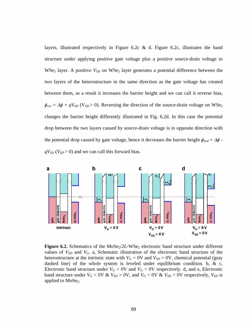
89
layers, illustrated respectively in Figure 6.2c & d. Figure 6.2c, illustrates the band
structure under applying positive gate voltage plus a positive source-drain voltage to
WSe2 layer. A positive VSD on WSe2 layer generates a potential difference between the
two layers of the heterostructure in the same direction as the gate voltage has created
between them, as a result it increases the barrier height and we can call it reverse bias,
ɸrev = Δɸ + qVSD (VSD > 0). Reversing the direction of the source-drain voltage on WSe2
changes the barrier height differently illustrated in Fig. 6.2d. In this case the potential
drop between the two layers caused by source-drain voltage is in opposite direction with
the potential drop caused by gate voltage, hence it decreases the barrier height ɸfwd = Δɸ -
qVSD (VSD > 0) and we can call this forward bias.
Figure 6.2. Schematics of the MoSe2/2L-WSe2 electronic band structure under different values of VSD and VG. a, Schematic illustration of the electronic band structure of the heterostructure at the intrinsic state with VG = 0V and VSD = 0V, chemical potential (gray dashed line) of the whole system is leveled under equilibrium condition. b, & c, Electronic band structure under VG > 0V and VG < 0V respectively. d, and e, Electronic band structure under VG < 0V & VSD > 0V, and VG < 0V & VSD < 0V respectively, VSD is applied to MoSe2.

90
6.3 Gate Voltage Dependence of I-VSD Characteristics of 2L-WSe2/MoSe2
As discussed before in details in chapter 6.2 and illustrated in figure 6.2 we could
electrostatically dope the interface of this heterostructure through a global back gate
voltage. As a result we observed an N+-N device behavior at low VSD and a well-defined
transition from insulating behavior at VG = -50 V to conducting behavior at VG = 10 V
through I-VG characteristics.
As the source-drain voltage VSD was increased, we observed a highly unusual
device response. Figure 6.6a shows a color map of the current I as a function of VSD and
VG. The I-VSD characteristics (Fig. 6.3b inset) measured in the low-current state (VG <
VON) exhibit very distinct behavior from those in the highly conducting N-type transport
regime. As the gate voltage increased, the forward bias I-VSD characteristics (VSD > 0 V,
Fig. 6.3b) exhibited a monotonic increase as a function of VSD. In contrast, Figure 6.3a
shows that the reverse bias (VSD < 0 V) current first increased sharply to a peak value
near VSD = - 4.8 V (bright feature, Fig. 6.3a) and then decreased at higher VSD. The non-
monotonic behavior in reverse bias emerged for VG > -36 V.
As gate voltage increased, the current peak remained at an approximately constant VSD
value. In the following, we examine the dependence of the interlayer current on source-
drain voltage, gate voltage, temperature, and optical illumination. In Figure 6.3c, the
reverse bias current peak emerges over a range of gate voltages corresponding to an
abrupt increase of the interlayer current I.

91
To examine the emergence of this peak more thoroughly, Figure 6.3d shows
differential conductance dI/dVSD vs. VSD as a function of gate voltage VG. Near VSD = -2.5
V, a maximum in the differential conductance, labeled gM, appears as VG increases.
Figure 6.3. Gate voltage dependence of the I-VSD and dI/dVSD characteristics in the 2D n+-n heterojunction device. a, Color map of I vs. VSD and VG (T = 340 K; heterostructure overlap area 4.3 µ m2). b, Forward bias I-VSD characteristics as a function of VG (increasing from dark purple to orange, labeled with vertical solid arrow). Inset, I-VSD characteristics at VG = 0 and VG = - 47 V (labeled). c, Reverse bias I-VSD characteristics as a function of VG. d, dI/dVSD vs. VSD characteristics (T = 340 K). NDC labels the negative differential conductance peak values (marked with open circles). gM is the maximum differential conductance.

92
In contrast, near VSD = -5.4 V, valleys in dI/dVSD vs. VSD evolve into prominent
negative differential conductance (NDC) for increasing VG (labeled with open circles).
The NDC occurs at a nearly constant VSD value as the gate voltage is increased. We
conclude that the onset of NDC, and thus the reverse bias current peak, directly correlates
with the VG dependent onset to unipolar electron conduction.
6.4 Temperature Dependence of I-VSD Characteristics of 2L-WSe2/MoSe2
The striking non-monotonic behavior of the reverse bias I-VSD characteristics also
arises as the temperature increases, and differs strongly from interlayer Zener tunneling
behavior4. We show in Figure 6.4 the I-VSD characteristics as a function of VG at several
temperatures. Below T = 340 K, the I-VSD characteristics exhibit no current peak in
reverse bias. At and above T = 340 K, however, the reverse bias current peak becomes
evident as VG is increased (Fig. 6.4a). Importantly, we also observed that the reverse bias
current increased much more rapidly with increasing temperature when compared to the
current at VSD > 0 V. At T = 360 K (Fig. 6.4b), the asymmetry in the I-VSD characteristics
is significant: the reverse bias current particularly at low negative VSD is approximately
two orders of magnitude larger than in forward bias. By rescaling the temperature-
dependent reverse bias interlayer current as T ln(I / T 2 ) , the data (for VG > VON) collapse
to a temperature-independent characteristic as a function of VSD (Fig. 6.4c). In forward
bias (Fig. 6.4d), a similar temperature-independent characteristic is observed, yet the
current must be rescaled as T ln(I / T ). In contrast to the temperature-independent current
expected for interlayer tunneling across the interface3, the reverse bias interlayer current I

93
∝ T 2exp(−1 / T ) increases sharply with temperature at low reverse bias, giving rise to a
current peak at increased temperatures.
We attribute the non-monotonic reverse bias current to interlayer e-h generation
by high-energy electrons transiting the atomic layer interface. In the e-h pair excitation
process requiring the lowest excess energy, an electron in WSe2 gains the combined
energy of the interlayer potential energy offset ΔEc0 and the kinetic energy of the source-
drain electric field to create a low-energy electron in MoSe2 plus an interlayer e-h pair
(Fig. 6.4e)
eW + Ke (VSD) → eMo + (eMo + hW). (6.1)
The subscript W or Mo indicates the layer into which the electron (e) or hole (h) is
transferred. The final three-body state includes an interlayer e-h pair produced at the
interface. The kinetic energy available to an electron eW in WSe2 is given by Ke = ΔEc,
where ΔEc (VSD) = ΔEc0 – e (αVSD) is the total potential energy drop for the interlayer
electron transfer process eW → eMo. The potential energy drop can be tuned by changing
VSD, and the phenomenological factor α accounts for additional voltage drop at the
contacts.
To model the device characteristics to include interlayer e-h multiplication, we
apply a conventional lucky electron model for hot electron injection through the 2D
semiconductor heterojunction (See 6.5 for a detailed representation). Ignoring
recombination of interlayer e-h pairs, the low bias current due to e-h pair multiplication
IM takes the form:

94
IM ∝ ΓM (kB T)2 exp(−K*e /kB T), (6.2)
Figure 6.4. Temperature dependence of the interlayer I-VSD characteristics. a, I-VSD characteristics at T = 310 K, 320 K, and 340 K (shifted vertically for clarity). VG increases from - 50 V to 10 V (dark purple to orange). b, I-VSD characteristics for increasing VG at T=360 K. c, Tln(I/T2) vs. VSD in reverse bias at T=300 K, 310 K, 320 K, 340 K, 360 K (VG =15 V). Inset gM/T vs. 1/T (VSD = -2.5 V, VG = 15 V). d, Tln(I/T) vs. VSD in forward bias at the same temperatures (VG = 15 V). d, (inset) I/T versus 1/T at VSD = 2.0 V, VG = 15 V. e, Electronic potential energy diagram for the heterojunction in reverse bias with electron-hole pairs generated at the MoSe2/2L-WSe2 interface. f, Electronic potential energy diagram for VSD > 0 V.

95
Where kB is the Boltzmann constant, and ΓM contains details about the impact
excitation probability and interlayer transit rate. The minimum kinetic energy required for
a hot electron to excite an interlayer e-h pair in reverse bias is given by
K*e =ΔE0
h −ΔE0c +2e (αVSD), (6.3)
where ΔE0h > ΔE0
c . When a negative VSD is applied, the potential energy gained by the
eW electron increases while the interlayer excitation energy decreases ΔEh = ΔEh0 – e
(αVSD) (Fig. 6.4e). For increasing reverse bias, the rapidly increasing current due to e-h
multiplication IM is overcome by the evolution of the recombination rate with VSD:
recombination increases with the reduction of ΔEh, and also increases with VG since there
are more electrons available to combine with the holes generated through impact
excitation. This competition results in NDC and a corresponding peak in the dark I-VSD
characteristics.
6.5 Interlayer Electron Transport of 2L-WSe2/MoSe2
In this section, we obtain the temperature and VSD dependence of the interlayer
current I by a straightforward calculation based on the electron transmission formalism5.
Following Chul-Ho Lee, et al.6, we model a 2D n-type, type II heterojunction in which
most of the voltage drop in the device occurs across the vertical junction, leaving no
appreciable potential barriers in the lateral transport direction within each semiconductor
layer. In our model, we assume these contributions to the functional form of the I-VSD
characteristics to be negligible, and later compare this assumption to experimental data.
We then evaluate the current in forward and reverse bias by assessing the rates of

96
electron transmission through the N- type heterojunction (Fig. 6.5), including the rate of
interlayer e-h pair multiplication. Our model assesses only carrier kinetic energy, and
asks: at what kinetic energy does a carrier have sufficient excess energy to produce
additional electron-hole pairs?
Our phenomenological model was developed to qualitatively explain the
temperature dependence of the I-VSD characteristics in the voltage regime just below the
appearance of NDC. Like conventional heterojunction devices, the current-voltage
characteristics are quite complicated, exhibiting several regimes that are described by
various microscopic processes. In conventional N+-N and P-N junctions for example,
different regimes often exhibit different ideality factors n. The commonly used ideality
factor is attributed to various mechanisms, but strictly speaking is a phenomenological
constant included to express the proportionality between electric potential drop and
applied voltage. In comparison to our data (section 6.5), we thus include a
phenomenological parameter α < 1, which quantifies the ‘lever arm’ between electric
potential energy and applied voltage VSD. In section 2.5 we calculated the density of
states for atomic layer transition metal dichalcogenides and from equation 2.13 found that
the density of states approaches a constant value for electrons near the bottom of the
bands, but depends linearly on the electron energy at high energies, which is completely
distinct from that at 2D electron gases.
6.5.1 Forward Bias Characteristics
Figure 6.8 shows a schematic of the potential energy landscape for electrons in

97
the heterojunction for VSD > 0 V. For kBT >> εF, we assume classical Boltzmann
distributions to evaluate how many right-moving electrons (i.e., electrons that are
transferred from MoSe2 into WSe2) transit the interface when a positive VSD is applied.
From the left side, we consider a charge carrier with energy that is just enough to get over
the potential barrier at the interface ΔE0c. From the diagram, this carrier has kinetic
energy ε – εF = ΔE0c – eVSD for VSD > 0 V.
In the forward bias interlayer transport process, conduction occurs through
electron states near the bottom of the conduction bands in both materials. In this case, the
density of states in both layers is approximately independent of energy. The interlayer
current results from counting only right-transiting electrons and is given by:
I+ = 𝑒𝑣𝜂!𝑔!(𝐸) 𝑔!"(𝐸) 𝑓(𝐸) 𝑑𝐸 !! (6.4)
where v = vF is the electron Fermi velocity, η0 is the transmission coefficient, gW(E) and
gMo(E) are the density of states in WSe2 and MoSe2, respectively, and f(E) is the electron
distribution in MoSe2.
Assuming eVSD, ΔE0c >> kBT, the interlayer current is then
I+ =Γ+ ( kB T) exp (-(∆E0
c -eVSD )/kB T (6.5a)
where
Γ+= !"!!!!!!! ! (∆E0
c+∆E0h) (∆E0
h+∆E0v). (6.5b)
Here, we model the system to have constant transmission coefficient η0 for carriers whose
total kinetic energy is sufficient to transit the barrier between the TMD layers.

98
Figure 6.5. Schematics of TMD band structure and interlayer electronic transport. a, energy band diagram of a 2D-TMD material with hyperbolic band structure, b, c, Electronic band structure of the MoSe2/2L-WSe2 under forward and reverse bias respectively, the area inside the vertical dashed line illustrates the heterojunction.
According to Figure 6.5, the band gap energy in WSe2 is approximately equal to
∆E0c+∆E0
h and in MoSe2 equal to (∆E0h + ∆E0
v).
Equation (6.5) indicates that in forward bias the normalized current I+/T should
exhibit an exponential decrease with 1/T, from which the activation energy ΔE0c can be
extracted. Equation (6.5) can also be re-expressed in terms of a temperature-independent
quantity that depends only on ΔE0c and VSD:
kBT ln I+/Γ+kBT =-∆E0c+eVSD. (6.6)

99
The forward bias I-VSD characteristics, when rescaled as T ln(I+/T) as in equation
(6.6), should collapse to a single characteristic. The current T ln(I+/T) vs. VSD exhibits
temperature independent behavior with a linear increase as VSD increases.
The data for all temperatures (Fig. 6.7d) indeed exhibit this behavior, collapsing
to a temperature-independent characteristic current T ln(I / T ) . We infer the conduction
band offset ΔE0c = 0.2 eV from an exponential fit of the forward bias current I/T as a
function of 1/T (Fig. 3.8d inset). The value obtained from transport measurements shows
excellent agreement with band structure calculations ΔE0 (theory) = 0.20 eV (Fig. 2.4).
The energy ΔE0c is the maximum kinetic energy available to a hot electron at VSD = 0 V
(Fig. 1.7a).
6.5.2 Reverse Bias Characteristics
In reverse bias, the temperature and VSD dependence of the interlayer current
serves as a signature of hot electron injection into MoSe2, while the thermally activated
behavior arises from the energetic threshold for e-h pair multiplication. The electron-hole
pair production process takes place in two steps: (1) a low-energy electron in WSe2 is
transferred into a high-energy state in MoSe2. (2) The high-energy (hot) electron in
MoSe2 decays and produces an interlayer e-h pair. As the reverse bias voltage is
increased, electron-hole pairs generated by high-energy electrons are separated in the
electric field and increase the device current. We first define the energy barrier for
additional electron generation due to e-h pair multiplication, and then evaluate the
interlayer current I that results from e-h pair multiplication when VSD < 0 V.

100
For interlayer transport from WSe2 (right) to MoSe2 (left), it is important to note
that electrons need not overcome a potential energy barrier, but instead may gain the
potential energy ΔE0c. In conventional devices, this leads to reverse bias saturation
current with weak dependence on VSD or temperature7. However, interlayer e-h pair
production requires a hot electron with a minimum excess kinetic energy, and thus
depends strongly on both VSD and temperature. From the schematic in Figure 3.9, the
minimum kinetic energy required for an electron to generate an interlayer e-h pair is
given by:
K*e =∆E0
h -∆E0c +2eVSD, (6.7)
where ΔE0h is the interlayer e-h pair excitation energy at VSD = 0 V. We note that when
VSD < 0 V, the potential energy that can be gained by an electron is increased ΔEc =ΔE0c
+e |VSD |, while the interlayer excitation energy is simultaneously decreased ΔEh =ΔE0h –
e |VSD |, resulting in equation (6.7).
In reverse bias, the energy difference between the conduction bands of the two
materials is large. Due to the electric field at the interface, low-energy electrons in WSe2
with approximately constant density of states are transferred into hot electrons in MoSe2
at high kinetic energy with density of states proportional to E (equation (2.13)). The
current due to interlayer e-h pair multiplication IM is then
IM ≈ 𝑒𝑣𝛾!!!"#!
!!!!!∞
!!
!!!!!𝑒𝑥𝑝 − !!!!
!!!𝑑𝐸; (6.8a)
=!"!! ∆!!!!∆!!!
!!!!! ! 𝐸𝑒𝑥𝑝!! − !!!!
!!!𝑑𝐸; (6.8b)

101
where we assume that the product of the transmission coefficient and impact excitation
rate γ0 is approximately constant above the kinetic energy threshold. Computing the
integral over the entire energy range and noting kBT >> εF, gives
IM = Γ! 𝐾!𝑇 ! 𝑒𝑥𝑝 !!!∗
!!!− 1 ; (6.9a)
𝛤! = !"!! ∆!!!!∆!!!
!!!!! ! . (6.9b)
In contrast to the forward bias current, there is an additional power of kBT in the reverse
bias current, which arises from the density of available electron states in MoSe2.
Equation (6.9) indicates that in the VSD and temperature regime in which e-h pair
multiplication is the dominant source of current, the reverse bias current can be re-
expressed in terms of a temperature-independent quantity that depends on ΔE0h. The
reverse bias I-VSD characteristics, when rescaled as T ln(IM/T2) as in equation (6.9),
should collapse to a single line. In this case, the voltage dependence of T ln(IM/T2)
exhibits universal behavior, with a linear increase with VSD.
While equation (6.9) gives the temperature scaling of the current due to e-h pair
multiplication, an additional straightforward analysis is required to obtain ΔE0h. First,
note that equation (6.9) contains a VSD-independent term and a VSD-dependent term. In
order to isolate the activation energy ΔE0h, we simply take the derivative dIM/dVSD of
equation (6.9), giving
!!!/!!!"!!!!!
= exp −𝐾!∗/𝐾!𝑇 . (6.10)
Equation (6.10) indicates that the quantity (dIM/dVSD)/T vs. 1/T should exhibit an
exponential decrease, from which the activation energy K*e can be extracted.

102
6.6 Gate and Temperature Dependence of dlogI/dVG of 2L-WSe2/MoSe2
The model described in sections 6.3 and 6.4 makes a number of predictions that
can be compared to experiment. First, as the reverse bias voltage is increased, hot
electrons with kinetic energy that exceeds K*e may generate interlayer e-h pairs (Fig.
6.4e), which are subsequently separated into the constituent electron and hole. Impact
excitation is expected to generate additional conduction electrons at the interface. As a
consequence, the onset gate voltage VON is lowered for negative VSD, while it is not
affected for VSD > 0 V.
We examine the gate voltage dependence of the interlayer current to test this
conjecture. Figure 6.9a shows a color map of dlogI/dVG vs. VG and VSD taken at T = 340
K. At VSD > 0 V, we observed a vertical peak feature in the dlogI/dVG map that occurs
near VG = -36 V. We label this gate voltage, which remains constant in forward bias, as
V+ON in Figure 6.6a. Such standard behavior does not include the effects of e-h pair
multiplication. In contrast, horizontal line traces of dlogI/dVG in reverse bias (Fig. 6.6a
bottom) show that VON decreases approximately linearly with increasing negative VSD.
This response is consistent with the e-h pair production process of equation (1):
additional electrons generated in the MoSe2 conduction band increase the electron density
in the unipolar interlayer channel, thus lowering the gate voltage required for the onset to
conduction.
Our model also predicts that by reducing temperature, impact excitation and charge
multiplication are suppressed. To see this, Figure 3.10b shows the temperature evolution

103
Figure 6.6. Gate voltage, source-drain voltage, and temperature dependence of dlogI/dVG in the atomic layer semiconductor heterostructure device. a, Color map of dlogI/dVG vs. VG and VSD (T = 340 K). Top, dlogI/dVG vs. VG characteristic at VSD = 2.0 V. Vertical dashed line labels the maximum value of dlogI/dVG in forward bias, denoted . Bottom, dlogI/dVG vs. VG characteristics for increasing negative VSD from VSD = -1.0 V (yellow line) to VSD = -8.5 V (purple line). b, dlogI/dVG vs. VG and VSD for negative VSD. The gate voltage axis is shifted by (vertical dashed line) extracted at each temperature. c, Maximum values of dlogI/dVG extracted at each temperature. V*
SD labels the intercept of the linear fits of the maxima and .
of the dlogI/dVG maps in reverse bias. At each temperature, we extract the maximum
values of dlogI/dVG as a function of VG and VSD (Fig. 6.6c). At T = 300 K, the onset gate
voltage shifts only slightly below V+ON (vertical dashed lines Fig. 6.6c) as the reverse bias
VON+
VON+
VON+

104
VSD is increased, indicating that no additional charge is generated at the interface. Above
T = 320 K, as the source-drain voltage increases above the threshold V*SD = -1.2 V, the
onset gate voltage VON decreases approximately linearly with increasing negative VSD.
The appearance of this feature, in which VON decreases linearly with negative VSD,
correlates directly with the temperature-dependent increase of the interlayer current (Fig.
6.4).
The very low threshold voltage V*SD shown in Figure 6.4b highlights an important
aspect of hot carrier-enhanced e-h pair generation. The interlayer transport process eW →
eMo transfers a low-energy electron in the WSe2 conduction band into a hot electron
above the conduction band edge in MoSe2 (Fig. 6.5). Impact excitation generates
additional charge density only if the excess kinetic energy exceeds K*. VON is therefore
reduced below V+ON once the source-drain voltage exceeds a critical energy eV*
SD > 1.2
eV (labeled in Fig. 6.6c). The threshold voltage V*SD for interlayer e-h pair generation is
lower than the energy-conservation limit for excitation of intralayer bound e-h pairs in
either MoSe2 (ΔEMo/e = 1.57 V) or 2L-WSe2 (ΔEW/e = 1.46 V).
6.7 Power Dependence of I-VSD Characteristics of 2L-WSe2/MoSe2
So far in this chapter we explicitly discussed hot carrier-enhanced interlayer
impact excitation through electronic transport experiments of 2L-WSe2/MoSe2. Here we
study this phenomenon through optoelectronic experiments. Figure 6.7a shows interlayer
photocurrent characteristics measured as a function of temperature at low optical power
(17 µW) and λ = 900 nm. When VG < VON, the dark current (black line trace Fig. 6.7) is

105
strongly suppressed since the N+-N heterojunction formed at the interface is depleted of
conduction electrons. Under local optical illumination of the heterostructure, we observed
dramatic increase in the reverse bias photocurrent with increasing temperature. In
contrast, the photocurrent at VSD > 0 shows negligible temperature dependence. The
prominent enhancement of the reverse bias photocurrent is fully consistent with equation
(1): an optically excited eW electron in the conduction band of WSe2 undergoes efficient
multiplication into an eMo electron and additional e-h pairs.
Remarkably, we find that the MoSe2/2L-WSe2 photocells exhibit a responsivity
enhancement that exceeds 350%. To quantify the multiplication factor, we measured the
detailed power dependence at each temperature (power dependence for T = 300 K shown
in Fig. 6.7b) and examined the ratio of the responsivity R at elevated temperatures to that
at T = 300 K. Since impact excitation is suppressed at low temperatures, the ratio R350 /
R300 gives a lower bound estimate of the multiplication enhancement. Figure 6.10c shows
the multiplication enhancement factor R350 / R300 as a function of VSD for various optical
powers. At low power (blue data), the enhancement factor exceeds 3.5 and shows a clear
peak near VSD = -2.8 V. At high optical power (red data) the enhancement is reduced,
likely resulting from increased electron-hole pair annihilation or thermal effects. Of key
importance, the maximum multiplication near VSD = -2.8 V corresponds very closely to
the peak conductance gM due to e-h multiplication in the absence of light (Fig. 3.4d). This
direct correspondence further highlights the ultra-low VSD threshold for hot carrier-
enhanced impact excitation.

106
The extraordinary efficiency of the eW + Ke → eMo + (eMo + hW) process at
elevated temperatures is an unexpected result. Normally, relaxation mechanisms such as
optical phonon emission are very efficient for relaxing hot electrons, including those in
individual monolayer TMDs8. In contrast, the eW → eMo process observed here produces
hot eMo electrons that subsequently relax excess kinetic energy equal to ΔEh0.
Multiplication dominates over ordinary interlayer electron transfer, and thus the reverse
bias current depends sensitively on ΔEh0 and temperature. According to equation (2) in
section 3.8, IM contains a temperature-dependent pre-factor of (kBT)9. This factor arises
from the increased density of states available to hot eMo electrons during impact
excitation (Fig. 6.5), and does not arise in forward bias (section 6.5.1).
Figure 6.7. Interlayer photocurrent characteristics and multiplication enhancement in the 2D heterojunction photocell. a, Interlayer photocurrent vs. VSD at T = 300, 340, and 350 K with VG < VON; black line trace is the dark I-VSD characteristic. Optical illumination is focused at the heterostructure with a laser at λ = 900 nm, P = 17 µW. (see inset schematic) b, Interlayer photocurrent vs. VSD for increasing optical power at T = 300 K. Inset, photocurrent vs. power at VSD = -5 V. c, Multiplication factor determined from the ratio of the responsivities R350 / R300 at various optical power levels (labeled). Solid lines are Lorentzian fits used to determine the peak multiplication value.

107
The differential conductance in reverse bias is given by g = dIM/dVSD ≈ 2eIM / kBT
(Section 6.5.2 equation 10), suggesting a linear relationship between ln(g/T) and 1/T with
a slope of −Ke* . Figure 6.4c inset shows the data ln(gM/T) vs. 1/T over a range of
temperatures. From the slope of the linear fit (−Ke*) and equation (6.3) in section 6.7, we
obtain the interlayer e-h pair excitation energy ΔEh0 = Ke
* + ΔEc0 = 1.0 eV. The value
obtained from transport data agrees well with ΔEh0 (theory) = 0.94 eV (Fig. 2.5).
Hot electron impact excitation results in a highly efficient energy relaxation
process that differs strongly from conventional impact ionization. In the TMD
heterostructure photocells, no avalanche breakdown behavior is observed, giving
additional insight into the origin of the NDC in Figure 6.3. While NDC is often attributed
to tunneling behavior, here the NDC is due to the competition between multiplication and
e-h pair recombination. Recent measurements of 2D heterostructures have suggested that
Shockley-Read-Hall (SRH) and Langevin processes dominate the unusual recombination
of interlayer e-h pairs9-11. In the devices demonstrated here, the multiplication-
recombination competition results in a peak in the dark I-VSD characteristics (Fig. 6.3c)
and a corresponding reduction of the multiplication enhancement factor at high negative
VSD (Fig. 6.10b). While in standard semiconductors, competing energy relaxation
mechanisms restrict carrier multiplication to extremely large biases12; interlayer impact
excitation dominates at very low applied VSD bias. Such remarkable behavior may enable
enhanced energy transfer, power conversion efficiency, and light emission processes that
take advantage of the layer-indirect nature of 2D heterostructure e-h pairs.

108
6.8 Comparison of the Model to Experimental Data
Our simple model agrees well with the temperature dependence observed in
Figure 6.7, but may not capture all details of the interlayer transport processes at all
biases. Importantly, we note that the model agrees well only within the voltage regime
leading up to the onset of NDC (-3 V < VSD < -0.5 V). Within this voltage regime, α
remains constant and can be extracted from the temperature-dependent data such as that
shown in Figure 6.4c. The obtained value for the device of Figure 6.3, α = 0.2, is typical
for TMD heterostructure devices studied here, and likely arises from a combination of
contact resistance, resistance drop across the individual materials, as well as intralayer
recombination processes. Figure 6.8 shows I-VSD characteristics over the range of
voltages that can be well described by our model. The rescaled current Tln(I/T2) changes
approximately linearly with VSD over the range -3 V < VSD < -0.5 V and for increasing
values of VG near the onset threshold. Tln(I/T2) also increase linearly with VG over the
range of voltages -37 V < VG < -31 V, which is precisely the onset regime. The linear
dependence on VSD, and the corresponding constant value of α over this voltage regime
strongly suggests that the potential drop across the interface scales proportionally to the
applied voltage in a similar way over the entire voltage range near the onset to NDC. Of
importance, the voltage drop along the lateral direction of the interface may depend on
the device current, which in turn influences the voltage drop across the junction. While
this is not explicitly treated in our model, the details of this effect are captured
qualitatively in the phenomenological factor α. While a detailed treatment would require
microscopic understanding of the interlayer transfer rates and the exact origins of α, we

109
exclude this subtle effect since α remains constant over the voltage regime of interest,
thus allowing us to capture the basic temperature dependent behavior. At very low bias
(VSD < 0.5 V), the regime in which the current does not match the behavior in our model,
α is difficult to extract since the current does not increase exponentially. As suggested in
Chul-Ho Lee, et al.13, this likely results from the lateral voltage drop or the non-
exponential behavior due to recombination effects. At very high voltage (above NDC),
we observe an additional feature of carrier multiplication: an enhancement of the device
noise due to impact excitation.
Figure 6.8. Interlayer current-voltage characteristics in the transport regime near the onset to NDC. a, Reverse bias I-VSD characteristics, rescaled as described in Section 3.9.1. b. I-VG characteristics with the same rescaling shown at various values of VSD.
At T = 360 K, the efficiency of impact excitation increases, leading to significant
noise at high voltage. While this behavior may result from random current fluctuations
due to carrier multiplication, it is not well described by the hot-carrier enhanced impact

110
excitation model below the threshold. Future work will focus closely on exploring the
impact excitation noise factor to explore noise in the carrier multiplication process.
6.9 Photoresponse of the Atomic Layer Hetero-Junction
For the assessment of the multiplication factor, we were very careful to
photoexcite only within the WSe2 absorption edge while avoiding optical absorption in
the (overlapping) low energy tail of the MoSe2 absorption peak. Absorption in MoSe2
may result in complicated interlayer transfer processes and additional state filling that
may skew the determination of the multiplication factor. From Figures 5.2 and 5.4, we
show that the heterostructure exhibits somewhat weak, but easily measured
photoluminescence and photocurrent response at photon energy 1.38 eV (corresponding
to λ = 900 nm). While this energy is slightly below, but still within the absorption peak of
the eW transition, we chose this wavelength to avoid as much as possible any absorption
in the low energy tail of the MoSe2 absorption edge, which begins to become non-
negligible as the photon energy increases above 1.4 eV (Figure 5.4).
Figure 6.9 shows photocurrent I-VSD characteristics taken at increasing photon
energies and T = 300 K (in the regime of inefficient impact excitation) with the laser
power fixed at P = 17 µW. While the overall photoresponse at 1.38 eV is comparatively
weak, the photocurrent results primarily from absorption in WSe2 rather than combined
absorption within the absorption bands of WSe2 and MoSe2. As the absorption of MoSe2
becomes important at higher energies, the overall photoresponse increases proportionally.
At higher photon energies, a careful assessment of the multiplication factor is less

111
dependable, as it must include the additional effects of current flow and interlayer
transfer caused by absorption in both layers. Future work will examine the detailed
photon energy dependence of impact excitation process by probing the intricate
dependence of photocurrent on photon energy, voltage, and temperature.
Figure 6.9. Wavelength dependence of the interlayer photocurrent-voltage characteristics at T = 300 K. Photocurrent (absolute value) vs. VSD measured as a function of decreasing wavelength (increasing photon energy) at fixed power = 17 µW. Photon energies are Eph = 1.38 eV, 1.45 eV, 1.57 eV, 1.62 eV, and 1.74 eV from bottom to top. For comparison, the black line trace is the same data shown in main text Figure 6.1a (T = 300 K, Ephoton = 1.38 eV).
6.10 2D-TMD N+-N Heterojunction Characteristics
The global back gate voltage VG allows electrostatic doping of the MoSe2/2L-

112
WSe2 interface, which is produced by mechanical exfoliation of bulk TMD crystals
followed by van der Waals-mediated pick-up, dry transfer, and high vacuum annealing
(See sections 3.4 & 3.5 for details). Assembling the individual TMDs into a
heterostructure results in a built-in potential energy difference across the interface
characterized by the band offset energy ΔEc0 (ΔEv
0) of the two conduction (valence)
bands (Fig. 6.10a). An electron transiting the interface from WSe2 into MoSe2
experiences the potential energy drop, while an electron travelling in the opposite
direction must gain sufficient kinetic energy to overcome the potential energy barrier
ΔEc0. At the heterostructure interface, the energy difference ΔEh
0 between the highest
valence band and lowest conduction band is the minimum energy required to excite an
interlayer e-h pair.
Figure 6.10b shows the current I as a function of gate voltage VG at source-drain
voltage VSD = 0.65 V. The I-VG characteristic demonstrates ordinary unipolar electron-
type (N- type) semiconductor heterojunction behavior: current that increases
monotonically at low VSD and a well-defined transition from insulating behavior at VG = -
50 V to conducting behavior at VG = 10 V. From the I-VG characteristic, we compute
dlogI/dVG and find the maximum, which determines the onset gate voltage VON = -35.5 V.
For gate voltages above VON, electrons are transferred through the N+-N heterojunction
formed at the interface of the heavily electron-doped (N+) MoSe2 and lightly electron-
doped (N) WSe2.

113
Figure 6.10. Band structure, and current-voltage characteristics of the 2D semiconductor heterostructure device. a, Electronic energy band diagram of the N+-N heterojunction at VSD = 0 V, showing the conduction bands (CB), valence bands (VB), and chemical potential µc in equilibrium (dashed gray line). b, Device current I (black) and dlogI/dVG (blue) vs. gate voltage VG (VSD = 0.65 V; T = 340 K).

114
REFERENCES
1. Barati, F. et al. Hot carrier-enhanced interlayer electron–hole pair multiplication in 2D semiconductor heterostructure photocells. Nat. Nanotech. 12, 1134–1139 (2017).
2. Lee, C. et al. Atomically thin p–n junctions with van der Waals heterointerfaces. Nat. Nanotechnol. 9, 676-681 (2014).
3. J. Kang, S. Tongay, J. Zhou, J. Li and J. Wu, Band offsets and heterostructures of two-dimensional semi- conductors, Appl. Phys. Lett., 2013, 102(1), 012111–012114.
4. Nourbakhsh, A., Zubair, A., Dresselhaus, M., & Palacios, T. Transport Properties of a MoS2/WSe2 hterojunction transistor and its potential for application. Nano Letters 16, 1359-1366 (2016).
5. Datta, S., Electron Transport in Mesoscopic Systems. (Cambridge university
Press, Cambridge, 1995).
6. Lee, C. et al. Atomically thin p–n junctions with van der Waals heterointerfaces. Nat. Nanotechnol. 9, 676-681 (2014).
7. Furchi, M. M., Pospischil, A., Libisch, F., Burgdörfer, J. & Mueller, T.
Photovoltaic effect in an electrically tunable van der waals heterojunction. Nano Lett. 14, 4785-4791 (2014).
8. Movva, H. C. P. et al. High-mobility holes in dual-gated WSe2 field-effect
transistors. ACS Nano 9, 10402-10410 (2015).
9. Rivera, P. et al. Valley-polarized exciton dynamics in a 2D semiconductor heterostructure. Nat. Commun. 6, 1-6 (2015).
10. Rivera, P. et al. Observation of long-lived interlayer excitons in monolayer
MoSe2– WSe2 heterostructures. Science 351, 688-691 (2016).
11. Lee, C. L. et al. Atomically thin p–n junctions with van der Waals heterointerfaces. Nat. Nanotechnol. 9, 676-681 (2014).
12. Sze, M. & NG, K. K. Physics of Semiconductor Devices. (Wiley-Interscience
publications, United States, 1963).
13. Lee, C. et al. Atomically thin p–n junctions with van der Waals heterointerfaces. Nat. Nanotechnol. 9, 676-681 (2014).

115
CHAPTER 7
PHONON-ASSISTED ANTISTOKES UPCONVERSION IN A VAN DER WAALS
HETEROSTRUCTURE P-N JUNCTION PHOTOCELL
7.1 Laser Cooling of Semiconductors
Laser cooling of solids, and more specifically semiconductors, has recently
attracted a lot of interest. Laser cooling is most commonly used for cooling and trapping
atoms and ions to extremely low temperatures. Surprisingly, the concept of laser cooling
of solids or optical refrigeration was proposed by Pringsheim in 19291, nearly half a
century before Doppler cooling of atoms was contemplated and well before the invention
of the laser. In the solid phase, thermal energy is due to vibrational modes of the lattice
(phonons). For a given electronic transition, photons in the low energy (red-shifted) tail
of the absorption maximum may be absorbed, followed by spontaneous emission of more
energetic (blue-shifted) photons. During the emission process, the energy difference
between absorption and emission is extracted from lattice thermal vibrations (phonons)
through a process known as anti-stokes process. In order to demonstrate laser cooling in
any system, the key requisite is to demonstrate the anti-stokes absorption processes.
Historically, material purity problems prevented the observation of this type of
laser cooling until 1995, when it was first demonstrated in ytterbium-doped glass2, a rare
earth doped material (RE). Soon after this successful observation of net cooling, attention

116
was directed towards cooling matter in various condensed phases, beyond RE materials.
The desire to achieve much lower temperatures than RE doped systems, as well as the
search for direct integration into existing semiconductor-based devices, has placed the
focus of numerous theoretical and experimental investigations of laser cooled solids on
semiconductors. Experiments recently conducted on bulk GaAs heterostructures3, as well
as CdS bulk and nanostructures4, have shown promising results, motivating a strong
interest in laser cooling of semiconductors even without the demonstration of net cooling.
Semiconductor cooling could provide more efficient pump light absorption, the potential
of much lower temperatures, and the opportunity for direct integration into electronic and
photonic devices for low temperature operation. In principle, the existence of a
continuum of states outside the direct band gap characteristic of many semiconductors
could allow such materials to get much colder (temperatures ~10 K and below) than RE
materials (limit of ~100 K)5.
7.2 Preliminary Optical Characterizations
In this chapter we study phonon assisted anti-stokes absorption in a 2D
heterostructure photocell composed of a bilayer tungsten diselenide (2L-WSe2) stacked
on top of a monolayer molybdenum diselenide (MoSe2) on a Si/SiO2 substrate integrated
into a field effect heterojunction device. A back-gate voltage controls the doping level of
carriers between the layers of the heterostructure. Source-drain contacts give electrical
access to each layer in order to apply voltage to one layer and collect the interlayer
current from the other (Fig. 7.1a).

117
The heterostructure studied here is unique in that two atomically thin materials
form an interface between atomic systems with many fewer atoms than bulk solid-state
systems. The first step towards exploring anti-stokes absorption is to be able to make
high quality devices exhibiting a high level of control over different parameters of the
system. In chapter 3 we discussed in detail the process to make very clean and high
quality devices. We studied the characteristics of this heterostructure when it forms an
N+-N heterojunction (see Chapter 1 section 5.1). We also discussed how a P-N junction
(see Chapter 1 section 5.2) can be formed by tuning the Fermi level, giving us the ability
to electrostatically tune the carrier density at the interface. In the P-N junction regime, we
uniformly tune the heterostructure, balancing electrons and holes to reach the charge
neutrality condition. As we will show, under this charge neutral condition, we are able to
more fully explore phenomena like anti-Stokes absorption.
Figure 7.1b illustrates the Raman spectra taken from both the individual layers and the
heterostructure. We used a Horiba LabRAM HR spectrometer with an excitation of 532
nm, with working range of 100 cm-1 to 9700 cm-1. Measurements are performed at room
temperature with the power of excitation laser at 2 mW. For the monolayer MoSe2 we
observed a very active mode at 30 meV (241 cm-1), and another mode at 36 meV (289
cm-1). The first Raman active vibrational mode is assigned to an out of plane vibration of
Aˊ while the second not very active mode to an in-plane vibration of E12g, For bilayer
WSe2 we found a very active Raman mode at 31 meV (250 cm-1), and two other modes at
31.7 meV (256 cm-1) and 38 meV (308 cm-1).

118
Figure 7.1. Device configuration, and Raman Spectra. a, (top) Schematics of the atomic layer heterostructure (bottom) and the n-p heterojunction device with a Si/SiO2 back gate and source drain electrodes (heterostructure overlap area 6 µm2). b, Raman (λ = 532 nm) from MoSe2 (green), 2L-WSe2 (blue), and the heterostructure (black). b, (inset) Raman zoomed in closeup right around the very active area (30 meV).
Our measurements show excellent agreement with previous studies6-8, attributing
these vibrational modes to monolayer MoSe2 and bilayer WSe2. The first modes near 30
meV in WSe2 are assigned to E12g and A1
g respectively7,8. In E12g vibrational mode two in
phase Se atoms oscillate in opposite to a W atom at each layer and the two layers
oscillate laterally opposite to one another, while in A1g mode Se atoms oscillate in
opposite phase, out of plane with respect to W atoms. Raman spectra taken from the
heterostructure (black line) has a contribution of both layers, and it shows the feature of
the constituent materials and nothing else. According to figure 7.1c the most dominant
feature of Raman is around 30 meV, and the inset shows details of these features on a log
scale. According to reported literature6,7, these features are due to low frequency optical
phonon modes in the atomically thin system.

119
7.3 Spectral Imaging of High-Energy Excitation
Using the custom-built instrumentation presented in chapter 4, we fix a Gaussian
beam on the overlapped region of the heterostructure and tune the photon excitation
energy within a range between 1.37 - 1.55 eV (equivalent to wavelength within 800-900
nm) while measuring the interlayer photocurrent. Figure 7.2a shows the interlayer
photocurrent vs. photon excitation energy and gate voltage. Tuning the system to positive
gate voltage, the device is in the N-N configuration, and we observe several photocurrent
features as a function of photon energy. Moving towards zero gate voltage values, these
features disappear as we reach the charge neutral condition. As the gate voltage is tuned
in the negative direction, we again observe photocurrent features as the device enters the
P-N configuration.
To examine this behavior more carefully, Figure 7.2b shows the photocurrent as a
function of photon excitation energy taken at VG = -2 V from figure 7.2a. We observe a
feature at 1.53 eV right around the PL peak position of MoSe2. Tracking this feature
down over gate voltage (figure 7.2c), we observed no redshift. Neutral exciton does not
change with respect to electrostatic doping while charged exciton does; hence this feature
is labeled the neutral exciton of MoSe2 (X0Mo). The second feature n figure 7.2 b is
observed at 1.49 eV, with a redshift of the amount of 21 meV (Fig. 7.2 c). This feature is
consistent with MoSe2 trion peak (X+Mo) in two ways, first that it happens in the right
energy as other people have seen10, and second it redshifts like we would expect trions to
redshift11. The third feature is observed at 1.44 eV with the redshift of 54 meV, consistent

120
Figure 7.2. Gate voltage dependence of the excitation photon energy of the P-N atomic layer heterostructure under high excitations. a, Color map of excitation energy (1.37 eV to 1.55 eV) vs. VG at a fix VSD = +6 v (T = 300 K). b, Interlayer photocurrent vs. excitation photon energy that shows the existence of three peaks, neutral exciton peak in MoSe2 at 1.52 eV, positive exciton peak in MoSe2 at 1.49 eV, and positive exciton peak in WSe2 at 1.44 eV. c, Red shift of the peak positions versus gate voltage, neutral exciton in MoSe2 (in dark green), positive exciton peak in MoSe2 (in medium green), and positive exciton peak of WSe2 (in blue). with charged exciton of WSe2 (X+
W). The important point here is that by tuning the gate
voltage from -20 V towards zero we are basically pulling ions out of the system and
depleting the system completely from ions, so by the time that we reach -2 volts all we
are left with are primarily the neutral excitons. This is the gate voltage where the most
asymmetric diode characteristic of the device (P-N junction behavior) happens in the
system (discussed in details in section 7.5).
7.4 Spectral Imaging of Low-Energy Excitation
Being able to deplete the system from charged excitons by moving towards VG = -
2V we are only left with neutral excitons at the interface of the heterostructure.
Observation of antistokes process requires having a clean system free from charged
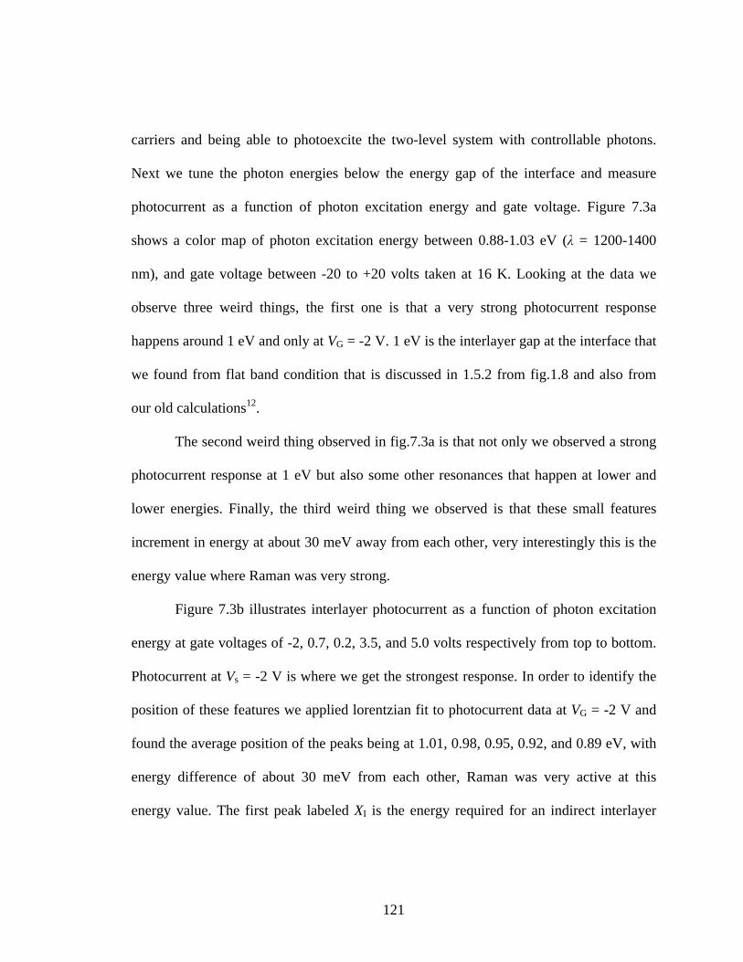
121
carriers and being able to photoexcite the two-level system with controllable photons.
Next we tune the photon energies below the energy gap of the interface and measure
photocurrent as a function of photon excitation energy and gate voltage. Figure 7.3a
shows a color map of photon excitation energy between 0.88-1.03 eV (λ = 1200-1400
nm), and gate voltage between -20 to +20 volts taken at 16 K. Looking at the data we
observe three weird things, the first one is that a very strong photocurrent response
happens around 1 eV and only at VG = -2 V. 1 eV is the interlayer gap at the interface that
we found from flat band condition that is discussed in 1.5.2 from fig.1.8 and also from
our old calculations12.
The second weird thing observed in fig.7.3a is that not only we observed a strong
photocurrent response at 1 eV but also some other resonances that happen at lower and
lower energies. Finally, the third weird thing we observed is that these small features
increment in energy at about 30 meV away from each other, very interestingly this is the
energy value where Raman was very strong.
Figure 7.3b illustrates interlayer photocurrent as a function of photon excitation
energy at gate voltages of -2, 0.7, 0.2, 3.5, and 5.0 volts respectively from top to bottom.
Photocurrent at Vs = -2 V is where we get the strongest response. In order to identify the
position of these features we applied lorentzian fit to photocurrent data at VG = -2 V and
found the average position of the peaks being at 1.01, 0.98, 0.95, 0.92, and 0.89 eV, with
energy difference of about 30 meV from each other, Raman was very active at this
energy value. The first peak labeled XI is the energy required for an indirect interlayer
122
exciton to form at the interface. We then observed photocurrent suppression in the small
features at higher gate values where system is not charge neutral.
Figure 7.3. Low energy excitations. a, Color map of excitation energy vs. VG (T = 16.7 K). b, Interlayer photocurrent vs. excitation energy characteristics as a function of gate voltage.
7.5 2D-TMD P-N Heterojunction Characteristics
We can also integrate TMDs into semiconductor photodiodes and study the
optoelectronic characteristics. The electronic energy band diagram of a similar
heterostructure incorporated into a photocell device is shown in figure 7.4a. A band offset
between the two conduction (valence) bands at VSD = 0 V results from the built-in
potential energy difference across the interface. The energy gap between the lowest
conduction band and the highest valence band in the system is large enough to form an
interlayer exciton (XI) when photo-exciting the device. Chemical potential at equilibrium

123
lives in a medium regime between the lowest conduction and highest valence bands,
which forms a charge neutrality condition.
Applying a positive back gate voltage, shifts the Fermi level up by increasing the
electron concentration in the system, making both layers N-type (MoSe2 more N-type
than WSe2), creating an N+-N heterojunction photocell (discussed in section 1.5.1). Now
we apply negative gate voltage to the device, it shifts the Fermi level down by increasing
the hole concentration in the system, so the Fermi level would be between the conduction
band edge of MoSe2 and the valence band edge of WSe2, making MoSe2 more n-doped
with electrons as the majority carriers and WSe2 more P-doped with holes accumulation
at the band edge, creating a P-N heterojunction photocell. Black arrow in figure 6.4a
labeled XI indicates the photogenerated interlayer excitons in which its electrons belong
to MoSe2 layer and holes to WSe2 layer.
Spatially distributed charge at the interface of the heterostructure is shown in
figure 6.4b top. Applying a source-drain voltage (figure 7.4c) can tune the potential drop
(ɸ), to reduce the potential barrier width and make the carriers transfer easier (forward
bias behavior of a rectifier) or increase the barrier width (the behavior of a rectifier under
reverse bias). If the applied VSD is large enough it can flatten the bands by taking ɸ to
zero, in this case the voltage is called flat band voltage2. Flat band voltage is proportional
to the activation energy needed to generate an interlayer exciton ɸ = XI – eVSD, when ɸ =
0, XI = eVFB. A color map of the photocurrent with the excitation wavelength of
λ = 800 nm, as a function of VSD vertical axis and VG horizontal axis is shown in figure
6.5a, data is taken at low temperature of 16.7 K.

124
Figure 7.4. Band structure, and interlayer charge transfer at the P-N junction of 2L-WSe2/MoSe2. a, Electronic energy band diagram at VSD = 0 V, showing the conduction bands (CB), valence bands (VB), and chemical potential µc in equilibrium (dashed gray line). b, Spatially distributed charges at the interface, 2L-WSe2 is more p-doped and MoSe2 is accumulated with negative electrons. c, Electronic band diagram of the interface, applying VSD changes the height of the barrier ɸ.
Figure 7.5. Gate voltage dependence of I-VSD characteristics under illumination and in the absence of light. a, Color map of I vs. VSD and VG (T = 16.7 K) under illumination of λ = 800 nm. b, I-VSD characteristics taken from color map at VG = -2V, the onset of the P-N junction regime. b, (inset) absolute value of log scale of I-VSD with an arrow indicating the flat band voltage at 1 volts.

125
It shows an N+-N junction behavior at positive gate voltages and a P-N junction
characteristic in negative gate values. The onset of the P-N heterojunction behavior is
right around VG = -2 V. Figure 7.5b depicts photocurrent as a function of VSD at VG = -2 V
where it has the most asymmetric diode characteristic similar to a P-N junction.
In a P-N junction photodiode, the position where the I-VSD curve passes through
zero-photocurrent axis is called flat band voltage (explained in details in Fig. 7.4c), in the
fourth quadrant (where VSD > 0 and I < 0) electrical power is been generated within the
photodiode. The inset in figure 6.5b illustrates the absolute value of the I-VSD curve, it
shows that the cross over voltage is happening at VFB = 1V, it implies that the activation
energy needed in this system to generate an interlayer exciton is about 1 eV.
7.6 Phonon-Assisted Antistokes Shift
Band profile in the lateral direction is depicted in Figure 7.6a, it shows the
spatially indirect exciton formation at the interface of MoSe2 and 2L-WSe2, by
photoexciting the heterostructure with a controllable photon energy the electron in
conduction band of WSe2 undergoes indirect transition to the valence band of MoSe2 by
moving in real space shown by black arrow. From our old calculations we know that at
the interface of this heterostructure, the highest valence band edge of WSe2 is located at
the Γ valley of its first brillouin zone and the lowest conduction band edge of MoSe2
located at the K valley of its own first brillouin zone.
An electron transitioning from WSe2 to MoSe2 experiences an indirect momentum
exchange from the middle of the brillouin zone of the later to the corner of the brillouin

126
zone of the former shown in figure 7.6c. We found from the flat band condition shown in
figure 1.8 that this interlayer gap is about 1 eV; this is the activation energy an electron
needs to transition across the interlayer gap. The existence of phonons is required in this
system to both enable the momentum exchange for electrons, and to compensate the
energy difference for the space indirect transfer when we reduce the photoexcitation
energy.
Figure 7.6b shows electron transitions at different photon excitation energies. We
have a very clean system, no intermediate energy level, no ions, and we have one
transition of 1 eV from the highest valence band of WSe2 |0,0> (ground state) to the
lowest conduction band of MoSe2 |1,0> (first excited state) shown by XI (interlayer
exciton). Based on Born-Oppenheimer approximation we can separate the contribution of
electrons and phonons in an energy level, such that electronic ground state can consist of
several excited phononic states.
The second peak in figure 7.6b is observed with a photoexcitation of 30 meV
smaller than the first peak. We argue that phonons with energy of 30 meV are assisting
this antistokes process to happen in the system by compensating the energy difference
neede to generate an interlayer exciton. Consequently three more peaks each with photon
energy of 30 meV smaller than the previous one observed in figure 7.3a indicated by
arrows in figure 7.6b. The second transition takes an electron in its ground state
combined with a phonon at its first excited state to a state where electron would be in its
first excited state and phonon in its ground state, in another word phonons are being
consumed for this transition to happen.

127
We argue that the energy difference for transitions is compensated by phonons of
energy 30 meV in the system, one, two, three and four phonons respectively are being
pulled out of the system and spent efficiently for an electron indirect transition between
the states. This number is in perfect agreement with our Raman measurements shown in
figure 7.1b, where we observed the strongest peak with energy 30 meV an indication of
the existence of low frequency optical phonons in the system. These phonons in the
system are assisting the anti-stokes processes in this 2D-TMD based semiconductor
heterostructure photocell.
Figure 7.6, Band profile, two-level system transitions, and E-K diagram of the heterointerface of 2L-WSe2/MoSe2. a, Band profile in the lateral direction, a photon with controllable energy photoexcites the heterointerface and generates indirect interlayer excitons. b, Two-level system of the interface, XI is an indication of interlayer exciton. Arrows from phononic excited states are representing phonon-assisted antistokes shifts. c, E-K diagram of the first BZ of the interface, the top BZ belongs to MoSe2 layer with the lowest conduction band located at K point valley while the bottom BZ belongs to WSe2 layer with highest valence band located in Γ point valley.
128
REFERENCES
1. Pringsheim, P., Zwei Bemerkungen über den Unterschied von Lumineszenz- und Temperaturstrahlung. ZeitschriftfürPhysikAHadronsandNuclei 57,739-746, (1929).
2. R. I. Epstein et al., Observation of laser-induced fluorescent cooling of a solid.
Nature (London) 377, 500 (1995).
3. Sheik-Bahae, M., & Epstein, R. I., Can laser light cool semiconductors?. PRL 92, 2474031-4 (2004).
4. Zhang, J., Li, D., Chen, R., & Xiong, Q., Laser Cooling of a Semiconductor by 40
Kelvin: An Optical Refrigerator Based on Cadmium Sulfide Nanoribbons. Proc. of SPIE 8638 863808-2 (2013).
5. Seletskiy, D. V., et al., Laser cooiling in solids: advances and prospects. Rep.
Prog. Phys. 79 096401 (2016).
6. Tonndorf Ph., et al., Photoluminescence emission and Raman response of monolayer MoS2, MoSe2, and WSe2. OPTICS EXPRESS 4909, 21 (2013).
7. Hong, X. et al. Ultrafast charge transfer in atomically thin MoS2/WS2
heterostructures. Nat. Nanotechnol. 9, 682-686 (2014).
8. Rivera, P. et al. Valley-polarized exciton dynamics in a 2D semiconductor heterostructure. Nat. Commun. 6, 1-6 (2015).
9. Ross J. S., et al., Electrical control of neutral and charged excitons in a monolayer
semiconductor. Nature Communications 4, (2013).
10. Shepard G. D., et al., Trion-Species-Resolved Quantum Beats in MoSe2. ACS Nano, 11, 11550-11558 (2017).
11. Wang G., et al., Excitons in atomically thin transition metal dichalcogenides. Rev.
Mod. Phys. 90, 021001-0210025 (2018).
12. Barati, F. et al. Hot carrier-enhanced interlayer electron–hole pair multiplication in 2D semiconductor heterostructure photocells. Nat. Nanotech. 12, 1134–1139 (2017).
129
CHAPTER 8
CONCLUSION
We started chapter 1, with presenting the characteristics and basic operation of the
elementary building blocks of semiconductor electronic devices: semiconducting P-N
junctions. We then introduced light to study its interaction with matter within these
junctions: P-N junction photodiodes. We aim to integrate a class of atomic layer
semiconductor known as transition metal dichalcogenides (TMDs) into semiconductor
photodiodes and study the optoelectronic characteristics. Before discussing that we
presented a brief theory of TMDs electronic band structure and studied 2L-WSe2/MoSe2
in particular through DFT calculations. To understand the electronic transport in these
devices we first studied the density of available electronic states (DOS) in conventional
2D electron gases. We then calculated the DOS of TMDs through their band dispersion.
Through these calculations we found that DOS is independent of energy states in
conventional 2D systems while it’s linearly proportional to energy states in 2D-TMDs.
We continued chapter 3 with presenting the procedure to wafer preparation,
exfoliation, making stacks and finally device fabrication. Dry transfer method is used for
making stacks, for device fabrication we used EBL, FIB and metal deposition methods.
An experimental instrumentation was necessary to perform measurements on these
devices. The supercontinuum scanning photocurrent spectroscopy microscope is designed
and developed for most of the work presented in this thesis. In chapter 4 we present the

130
development of this microscope by combining spatially and spectrally resolved laser
excitation techniques along with an electronic transport experiments platform.
Using advanced optoelectronic measurements, we discovered highly efficient
multiplication of interlayer electron-hole pairs at the interface of a 2L-WSe2/MoSe2
integrated into a field- effect heterojunction device, the results are discussed in chapter 6
of this thesis. Electronic transport measurements of the interlayer current-voltage
characteristics indicate that layer indirect electron-hole pairs are generated by hot
electron impact excitation at temperatures near T=300 K. By exploiting this highly
efficient interlayer e-h pair multiplication process, we demonstrated near-infrared
optoelectronic devices that exhibit 350% enhancement of the optoelectronic responsivity
at microwatt power levels. This efficient energy relaxation pathway that competes with
electron thermalization losses, make 2D semiconductor heterostructures viable for a new
class of hot-carrier energy harvesting devices that exploit layer-indirect electron-hole
excitations.
Through our novel spatially and spectrally resolved measurements (in chapter 7)
on these high quality 2D-TMD devices, we’ve been able to isolate the interlayer exciton
species through a phenomenon called phonon assisted antistokes process and have
identified an entirely new light-matter interaction within these states. We show that under
optimized experimental conditions phonon assisted anti-stokes absorption near the
interlayer exciton edge of a van der Waals semiconductor heterostructure composed of
tungsten diselenide and molybdenum diselenide become dominant, such that at low
photon energies near 1eV, we observed a strong photocurrent peak with several low

131
energy echoes spaced by 30 meV below this fundamental absorption feature. This
process, which we find to be highly efficient due to the alignment of the exciton dipole
moment to the atomic displacement of the out-of- plane optical phonon modes, marks the
first and most critical step toward laser cooling of atomic layer semiconductors.
Moreover, the anti-stokes absorption process observed here could enhance the efficiency
of next generation photovoltaics, since it converts vibrational energy into electronic
excitations using photons with energies that are lower than the band gap, manuscript is in
preparation.