Embed Size (px)
Citation preview

University of Groningen
Reduction of loss processes in polymer light-emitting diodesAbbaszadeh, Davood
IMPORTANT NOTE: You are advised to consult the publisher's version (publisher's PDF) if you wish to cite fromit. Please check the document version below.
Document VersionPublisher's PDF, also known as Version of record
Publication date:2016
Link to publication in University of Groningen/UMCG research database
Citation for published version (APA):Abbaszadeh, D. (2016). Reduction of loss processes in polymer light-emitting diodes [Groningen]:University of Groningen
CopyrightOther than for strictly personal use, it is not permitted to download or to forward/distribute the text or part of it without the consent of theauthor(s) and/or copyright holder(s), unless the work is under an open content license (like Creative Commons).
Take-down policyIf you believe that this document breaches copyright please contact us providing details, and we will remove access to the work immediatelyand investigate your claim.
Downloaded from the University of Groningen/UMCG research database (Pure): http://www.rug.nl/research/portal. For technical reasons thenumber of authors shown on this cover page is limited to 10 maximum.
Download date: 29-05-2018

CHAPTERONE
INTRODUCTION TO POLYMER LIGHT-EMITTINGDIODES
1.1 Introduction
Our daily life is strongly influenced by solid-state electronic products. Nowadays, alife without electronic products like computers, mobile phones, displays, solar energyharvesting systems, artificial intelligence, and so on is hard to imagine. All of theseproducts are assembled from solid-state electronic devices like transistors, diodes andsensors. Transistors are a key component of modern electronics, processors and chipsets are composed of a huge amount of this element that acts as a switch to generateand process electronic signals. On the other hand, optoelectronic devices are anotherbranch from solid-state electronics that can produce, harvest and detect light. Light har-vesting systems absorb sun light and convert it to electricity, also called photovoltaics.For these systems, there is a big demand in the entire world due to growing energydemand. Solar energy harvesting systems are very advantageous since solar energy isa free, clean and available energy source. Light producing systems, which opposite tophotovoltaics convert electricity to light, are used in lighting and displays. Unlike sil-icon (Si), for light-emitting diodes (LEDs) semiconductors with a direct band gap likegallium arsenide(GaAs) are being used. LEDs made of III-V semiconducting materi-als are very efficient and have very low energy consumption. Beside these advantages,highly sophisticated deposition systems are required to fabricate LEDs and this makesthe final product rather expensive. An emerging new class of semiconducting materi-als are conducting polymers, in 1977 it was discovered that polyacetylene can be madeconductive upon doping. This discovery opened a new field for electronic device fabri-cation. Although polyacetylene is not a stable chemical and also not easy to work with,but it still attracted a big attention from the scientific community to explore more stableforms of conducting organic materials. From that time, many conducting organics have
1

Chapter 1. Introduction to Polymer Light-Emitting Diodes
been investigated and synthesized for electronic applications. Generally, polymers areflexible as well as mechanically strong , which opens up new options for flexible andlightweight (opto)electronic devices. Compared to inorganic semiconductors these de-vices can be produced more cheaply. Polymers can be processed from solution, enablingroll-to-roll technologies similar to newspaper printing systems that allow for a high pro-duction speed. This makes them attractive especially for large-area devices as solar cellsand lighting panels, resulting in a new emerging field, plastic electronics.
1.2 Polymeric Semiconductors
A polymer is a large molecule composed of a repeating molecular unit called monomer.A wide variety of polymers exists, from synthetic plastics to DNA and proteins, whichall play a crucial role in our daily life. A small group from the wide range of polymersor plastics has conducting properties that can be used as active material in electronicdevices. The first conducting polymer was AsF5 and iodine doped polyacetylene, forwhich the 2000 Nobel Prize in chemistry was awarded [1]. Most well-known polymers indaily life are good insulators and are used to insulate electrical elements. Now the basicquestion is what makes a polymer or plastic an insulator or a conductor. The featurethat gives (semi)conducting properties to a polymer is the so-called bond conjugation,in other words an alternation of double and single bond between carbon atoms. Car-bon has 4 electrons in its outer shell that can form different hybrid orbital structures assp3, sp2 and sp. In the insulating polymers, carbon atoms are hybridized in four sp3
orbitals that all are identical and called σ bonds. While in the conducting polymers car-bon atoms are hybridized in three in-plane sp2 orbitals that make σ bonds with adjacentatoms (making the backbone of the polymer) and a non-hybridized pz orbital that is per-pendicular to the σ bonds. The pz orbitals of two adjacent atoms overlap and form πbonds in which electrons are delocalized. Figure 1.1 shows delocalized pz orbitals on asegment of polyacetylene that overlap from two neighboring carbon atoms and form πbond. The bonding level π, still occupied with electrons, is known in chemistry as thehighest occupied molecular orbital (HOMO). The anti-bonding level, π∗, being the firstempty energy level, is called the lowest unoccupied molecular orbital (LUMO). Theseenergy levels in a conjugated polymer, which consist of a repetition of molecular units,can be explained with one-dimensional periodic Bloch wave functions. Figure 1.2 (left)shows the energy diagram for such a system and the corresponding energy-momentum(E − k) plot. It is also illustrated how π bonds (HOMO) and π∗ anti-bonds (LUMO)form by superposition of wave functions from adjacent atomic orbitals. Bonding andanti-bonding levels, according to the pz orbital configuration/phase are schematicallyshown in Figure 1.2 (right). The more nodes the orbitals have, the higher the correspond-ing energy level is. Figure 1.2 shows the most stable superposition to the energeticallymost unstable superposition in accordance with pz orbitals and their phase.
An electron from HOMO can be excited to the LUMO by absorbing energy/light,leaving behind a hole in the HOMO. The opposite interaction may also occur by recom-
2

1.2. Polymeric Semiconductors
Figure 1.1: The chemical structure of polyacetylene which have double and single bond alterna-tion. Blue and red lobes show the overlap between pz − pz orbitals (wave-functions) making πbond; color difference shows the phase of wave-function.
bination of an electron in the LUMO with a hole in the HOMO thereby generating light.The HOMO-LUMO levels are equivalent to the valance and conduction band in solid-state physics, respectively and the energy difference between them can be compared tothe energy band gap.
The energy level for the LUMO (HOMO) of conjugated organic materials is in therange of −1 eV to −4 eV (−4.5 eV to −6.5 eV) below vacuum. The band gap of organicmaterials covers the ultraviolet to the visible light range. This makes them suitable ma-terials to be used in optoelectronic devices.
3

Chapter 1. Introduction to Polymer Light-Emitting Diodes
Figure 1.2: Schematic E− k plot for different pz molecular orbital orientation (perpendicular to thepolymer backbone) in polyacetylene, that makes π and π∗ bonds or HOMO-LUMO energy levels.(right) Schematically pz orbitals and their phase in blue and red colors are shown; according to thedegree of being in-phase of pz orbitals, energy levels can have different energies.
1.3 Polymers as Light Source
As discussed, conjugation is the key feature that makes one-dimensional polymermolecules (semi)conductive. Since these materials can be synthesized chemically, theirsolubility, absorption/emission spectrum, and charge transporting properties can be ad-justed by changing the conjugated main chain and the side chains. A set of conjugatedpolymers are listed in Figure 1.3 that we study in this dissertation. Poly(p-phenylenevinylene) (PPV) is a greenish yellow emitting polymer, which has vey poor solubil-ity in organic solvents. Hence, it is functionalized with different kind of side chainsthat increase the solubility and cause a red-shift in the emission. Of the PPV fam-ily, we specifically mention two well known polymers which have been investigatedwidely; poly (2-[3’-(3,7-dimethyloctyloxy)] 5-methoxy-p-phenylenvinylene)co(2-[3′-(3,7-dimethyloctyloxy)]-phenyl-p-phenylenevinylene), also known as super-yellow PPV(SY-PPV), [2] and poly[2-methoxy-5-(20-ethylhexyloxy)-p-phenylene vinylene (MEH-PPV). [3,4] SY-PPV, developed by Covion Semiconductors GmbH is commercially avail-able (Figure 1.3(a)). MEH-PPV is probably the most studied PPV derivative, being func-tionalized with ethoxy and methoxy side groups emitting orange light. This polymer hasserved as a work-horse for two decades to investigate the charge transport and photo-physical properties of conjugated polymers.
4

1.4. Physical Structure of Polymer Diodes and Fabrication
The discovery of another solution processable polymer, poly(9,9-dialkylfluorene)(PFO) [5,6] (Figure 1.3(c)), opened the door to fabricate blue emitting diodes. Upon addi-tion of benzothiadiazole (BT) moiety in the PFO backbone (Figure 1.3(d)), its band gapdecreases and the emission shifts to the green. Polyalkoxyspirobifluoren (PSF) is anotherPFO derivative that is widely investigated as blue emitting material and in combinationwith red and green dyes can be used to fabricate white light-emitting diodes (Figure1.3(e)).
Poly(9-vinylcarbazole) (PVK) is a large band gap polymer with a non-conjugatedbackbone, that has also been studied for application in OLEDs (Figure 1.3(f)). This poly-mer was already extensively studied in the past because it has been used as photorecep-tor in xerography. We have used this polymer not only as a host but also as electron-blocking layer in this dissertation. In PVK, conduction occurs through the conjugatedcarbazole parts that are attached to the non-conjugated polymer chain.
Figure 1.3: (a)poly(2-[3’-(3,7-dimethyloctyloxy)]5-methoxy-p-phenylenvinylene)co(2-[3’-(3,7-dimethyloctyloxy)]-phenyl-p-phenylenevinylene)(SY-PPV), (b) poly[2-methoxy-5-(20-ethylhexyloxy)-p-phenylene vinylene (MEH-PPV), (c) poly(9,9-dialkylfluorene)(PFO),(d)poly(9,9-dioctylfluorene-alt-benzothiadiazole), Poly[(9,9-di-n-octylfluorenyl-2,7-diyl)-alt-(benzo[2,1,3]thiadiazol-4,8-diyl)](F8BT), (e) polyalkoxyspirobifluoren (PSF) (PVK), (f)poly(9-vinylcarbazole).
1.4 Physical Structure of Polymer Diodes and Fabrication
In a PLED, a conjugated polymer is sandwiched between two electrodes, the cathodeand anode. Due to the very low mobility of organic semiconductors (< 10−7m2/Vs),
5

Chapter 1. Introduction to Polymer Light-Emitting Diodes
the thickness of the emissive layer must be limited in the order of 100 nm to keep theoperating voltage low. Upon application of a voltage higher than the band gap of thepolymer the cathode and anode inject electrons and holes into the polymer, respectively.Due to Coulombic attraction between electrons and holes they form a bound electron-hole pair that is called exciton.
Since the electrical charges play the main role inside an electronic device, it is cru-cial to study the charge transport and recombination processes in these devices. Organicand inorganic LEDs are bipolar devices, which means that electrons and holes simul-taneously flow in the semiconductor. In these bipolar devices, electrons flow throughconduction band or LUMO and holes through valence band or HOMO. For a betterunderstanding, it is important to study the transport of the electrons and holes indi-vidually. To investigate the transport properties of conjugated polymers, we thereforeneed to fabricate three types of devices: hole-only and electron-only devices, whicheach measure the hole or electron current separately and bipolar LEDs where also re-combination takes place. In order to measure the bulk properties of the polymer inthe hole-only (electron-only) device the injection electrode needs to be Ohmic. The col-lecting contact on the other hand should block injection of the opposite carrier into thedevice. For a bipolar LED both the contacts for electron and hole injection need tobe Ohmic. Figure 1.4 shows a schematic structure of hole-only and electron-only de-vices. For hole-only device the polymer is typically sandwiched between a spin-coatedpoly(3,4-ethylenedioxythiophene):poly(styrenesulfonic acid) (PEDOT:PSS) (CleviosTM PVP AI 4083) bottom contact and an evaporated MoO3/Al top electrode. Both electrodesare well-known hole injecting materials that have sufficiently high work functions forOhmic hole injection, while blocking the injection of electrons. For polymers with avery deep HOMO like PFO and F8BT, with a HOMO around −5.8 eV, PEDOT:PSS witha work function of −5.1 eV cannot form an Ohmic hole contact. For these polymersonly MoO3 insures Ohmic hole injection due to its very high work function of −6.7 eV.To measure the electron transport, the polymer layer is sandwiched between thermallyevaporated Al (which blocks injection of holes and electrons into the device) as bottomcontact and an evaporated Ba/Al (5/100nm) contact on a glass substrate, resulting in anelectron-only device.
For double-carrier devices, ITO/PEDOT:PSS is used as the anode and Ba/Al as thecathode, as shown schematically in Figure 1.5. In such a PLED generated excitons mighttransfer their energy to the electrodes instead of emission of a photon, which is an im-portant loss process in PLEDs. To prevent these losses additional layers are being placedbetween the emissive layer and the electrodes. By tuning of the HOMO and LUMO lev-els the injected carriers are then confined inside the active emitting polymer, as schemat-ically shown in Figure 1.5. As a result, efficiency of the PLED will be enhanced. In thefollowing chapters, we will discuss the applicability of such a multilayer device fromsolution processing in detail.
All PLEDs and single-carrier devices were fabricated on glass substrates with a pat-terned indium-tin oxide (ITO) layer. The substrates were cleaned, dried, and treatedwith UV-ozone. The emissive polymer and blocking polymer layers were spin-coated in
6

1.4. Physical Structure of Polymer Diodes and Fabrication
En
erg
y (
a.u
.)
LUMO
HOMO
Ban
d G
ap
LEP
Al
Trap states
Al
– –
Ba
– –––
––––––––
–
LEP
Al
Trap states
+ ++
PE
DO
T:P
SS
+ ++++
+
++ +
+
+
ITO
MoO3
Hole-Only Electron-Only
Figure 1.4: Schematically shown the hole-only (left) and electron-only (right) devices which eachmeasures only hole and only electron current respectively.
a nitrogen atmosphere from toluene and chlorobenzene solutions. To avoid side-effectsfrom pollutants like dusts and so on, we carried out all the experimental procedures forfabrication of devices in a cleanroom. After device preparation, steady state electricalmeasurements were carried out in a controlled N2 ambient using a computer-controlledKeithley 2400 source meter. Device light-output was simultaneously recorded with aHamamatsu S1336 silicon photodiode.
7

Chapter 1. Introduction to Polymer Light-Emitting Diodes
HTL
ETL
LEP
Trap states
++ ++
––
PE
DO
T:P
SS
+
Al
Ba
––––––
––
++ +
+
+ +++ +
+
–– –
–––
–– – ––
+
LEP
Al
Trap states
++ +
––
Ba
–
––
+
PE
DO
T:P
SS
+ ++++
– ––––
–– ––
+
–IT
O
EXCITON
Figure 1.5: (Left) Schematically shown a single layer PLED that polymer sandwiched between PE-DOT:PSS anode and Ba/Al cathode, (right) typical multilayer PLED which has two more polymerlayers to confine electrical charges inside the active emitting layer.
1.5 Charge Transport in Polymer Semiconductors
Conduction and charge carrier density in non-doped organic semiconductors are verylow. Therefore, injected charges into the organic device are not neutralized with countercharges, as is the case in a conductive medium. As a result upon injection of chargesa space-charge region is being formed. These space charges produce an electrostaticfield that limits the amount of the charges that can be injected into the device. Thistype of conduction that occurs in dielectric media is called space-charge limited (SCL)conduction and the measured current from such a device is called space-charge limitedcurrent (SCLC). Mott and Gurney formulated the SCL transport with accordance to theapplied voltage and device thickness [7]
J =98
ε0εrµV2
L3 , (1.1)
where ε0, εr is the vacuum permittivity and dielectric constant of the semiconductor,respectively. µ is the charge mobility in the material and shows how quickly a chargecarrier can move under an applied electric field; by definition where v = µE is theaverage drift velocity of the carriers. The mobility is an important material parameterthat determines the performance of electronic devices. The conductivity of a materials isproportional to the mobility and the amount of charge carriers; σ = neµ , where n is thecarrier density and e is the elementary charge value.
8
1.5. Charge Transport in Polymer Semiconductors
It has been demonstrated that Equation 1.1 can describe the trap-free hole transportin polymers like MEH-PPV, but only at low applied voltages and room temperature.When the applied voltage is higher, the current rises more rapidly with voltage thanwhat Equation 1.1 predicts. Initially, to explain this deviation, contrary to Mott-Gurneylaw that assumes a constant value for mobility, an empirical field-and temperature de-pendent mobility with a Poole-Frenkel like field dependence was proposed [8]
µ = µ0 exp(− ∆
kT
)exp
(γ√
E)
, (1.2)
where µ0 is the mobility when the temperature is infinite and electric field is zero, ∆ theactivation energy, k the Boltzmann constant, T the absolute temperature, E the electricfield, and γ is a field activation parameter. This equation was applied successfully todescribe the transport in PVK and other molecularly doped polymers. [9,10] However, ascientific justification for this empirical model was missing.
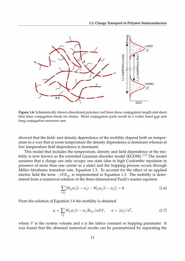
Conventional inorganic semiconductors like silicon (Si) and gallium arsenide (GaAs)exhibit a periodic crystal structure, where electrons and holes flow through delocalizedenergy bands. In contrast to inorganic semiconductors, conjugated polymers lack the 3Dcrystal order and band transport. Polymers are highly disordered materials and oftenform amorphous structures. Besides their structural disorder, polymer chains also con-tain defects and kinks where the conjugation is broken. As a result a polymer chain con-sists of conjugated segments that might have different length and therefore also slightlydifferent energy. As schematically shown in Figure 1.6, shorter conjugated segmentshave a wider energy gap than longer segments (quantum size effect), which can leadto spreading in site energies, also termed energetic disorder, of about 0.1− 0.2 eV. Theenergy offset leads to localization of the conjugated sites. To transfer a charge from onesite to another, electrons need to gain energy to hop. The energy to make a hop can beprovided by the absorbance and emission of phonons. Therefore, conjugated organicshave better conduction at higher temperatures. Conwell and Mott suggested this kind ofthermally assisted conduction for the first time in 1956, for impurity conduction in inor-ganic semiconductors. [11,12] Miller and Abrahams suggested a hopping rate, Wij, whichconsiders the probability of a carrier hopping from an occupied state, i, to an unoccupiedone, j. [13] The hopping rate depends on the difference in energy of each state, ε j− εi, andon the distance between those states, Rij, as
Wij = ν0 exp(−2α| ~Rij|
) exp(−
ε j − εi
kT
), ε j > εi
1 , ε j ≤ εi
, (1.3)
where ν0 is the attempt-to-jump frequency, α the inverse localization length and k theBoltzmann constant. The first exponential term represents the wave function overlap forstate i and j that determines the tunneling probability between the states. The secondterm describes the phonon distribution as a function of energy and temperature. In1993, Bassler by using Miller-Abrahams hopping rates, Equation 1.3, proposed a model
9

Chapter 1. Introduction to Polymer Light-Emitting Diodes
to explain the transport in positionally and energetically disordered polymers. [14] Heassumed that the energy distribution of the localized states may be approximated by aGaussian distribution (as shown in Figure 1.6) with a standard deviation;
DOS =N
2πσ2 exp(− ε2
2σ2
), (1.4)
where N is the total transporting sites and ε is the energy of a single state relative tothe center of the DOS. Such a formalism with Equation 1.3 is not analytically solvable.Therefore, Bassler used Monte Carlo method to calculate the charge transport in disor-dered semiconductors, presently known as the Gaussian Disorder Model (GDM). Theoutcome of his numerical simulations for the charge carrier mobility could be approxi-mated with an analytical formula of the form
µ = µ∞ exp
[−(
2σ
3kT
)2]×
exp(
C[(σ/kT)2 − Σ2]√
E)
; Σ ≥ 1.5
exp(
C[(σ/kT)2 − 2.252]√
E)
; Σ < 1.5, (1.5)
where µ∞ is the mobility at infinite temperature and amounts to interval 10−6 to10−5m2/Vs, C is a constant depending on lattice spacing, and Σ is a scale for positionaldisorder. The GDM model showed that the mobility depends on inverse square rootof temperature, which is non-Arrhenius. However, the predicted field dependence ofthe GDM is in agreement with experimental results only at high electric field (> 108
V/m). Gartstein and Conwell proposed the correlated disorder model (CDM), whichtakes the spatial energetic correlation between neighboring sites into account [15]. Thismodel could improve the agreement with experiment at low electric fields.
Studies conducted in the 80’s and mid-90’s considered mainly electric field and tem-perature dependence of the mobility. In 2003 also the dependence of the mobility oncharge carrier density was experimentally addressed. Since the density of carriers isrelatively low in diodes and with increasing voltage both the electric field and chargecarrier density are simultaneously enhanced, it is not straightforward to study the effectof carrier density on the mobility in a diode structure. However, by combining diodemeasurements with field-effect transistor (FET) measurements Tanase et al. showed thatthe measured mobility in FET device structure is much higher (orders of magnitude)than that in diode while the applied electric field between source and drain is muchsmaller. [16] Therefore, the enhancement of the mobility in a FET can be solely attributedto the enhancement of charge carrier density in the conductive channel due to appliedgate voltage, which controls the carrier density. [17,18] In diodes, hopping occurs throughthe sites in the tail of the DOS where the density of sites is low. While in a FET structure,upon application of a gate bias the tail of the DOS is filled and the Fermi-level approachesthe center of Gaussian DOS. Here there are more sites available for transport; and due tothis filling effect an enhanced mobility is measured. Model calculations by Pasveer et al.
10
1.5. Charge Transport in Polymer Semiconductors
**
*
Energ
y
H O M O
Long Conjugation (∗∗)
D O S
Short Conjugation (∗)
�
�L U M O
Figure 1.6: Schematically shown disordered polymer; red lines show conjugation length and shortblue lines conjugation break on chains. Short conjugation parts result in a wider band gap andlong conjugation narrower one.
showed that the field- and density dependence of the mobility depend both on temper-ature in a way that at room temperature the density dependence is dominant whereas atlow temperature field dependence is dominant.
This model that includes the temperature, density and field dependence of the mo-bility is now known as the extended Gaussian disorder model (EGDM). [19] The modelassumes that a charge can only occupy one state (due to high Coulombic repulsion inpresence of more than one carrier in a state) and the hopping process occurs throughMiller-Abrahams transition rate, Equation 1.3. To account for the effect of an appliedelectric field the term −eERijx is implemented in Equation 1.3. The mobility is deter-mined from a numerical solution of the three-dimensional Pauli’s master equation
∑i 6=j
[Wijni(1− nj)−Wjinj(1− ni)] = 0. (1.6)
From the solution of Equation 1.6 the mobility is obtained
µ = ∑i,j
Wijni(1− nj)Rijx/nEV, n = 〈ni〉/a3, (1.7)
where V is the system volume and a is the lattice constant or hopping parameter. Itwas found that the obtained numerical results can be parametrized by separating the
11

Chapter 1. Introduction to Polymer Light-Emitting Diodes
mobility dependence on carrier density and electric field, given by :
µ(T, n, E) ≈ µ(T, n) f (T, E), (1.8)
where the individual density and field dependent parametrization is given by :
µ(T, n) ≈ µ0(T, n) exp[−Cσ2] exp[
12(σ2 − σ)(2na3)δ
], σ =
σ
kT, (1.9a)
δ = 2ln(σ2 − σ)− ln(ln(4))
σ2 , (1.9b)
f (T, E) = exp
0.44(σ3/2 − 2.2)
√1 + 0.8(
eaEσ
)2− 1
, (1.9c)
where C = 0.42 , a is the intersite distance which is related to the transport site densityas a = N−1/3 , and µ0 is the mobility at the limit of zero field, zero carrier density andinfinite temperature. This model, in the limit of zero density is equivalent to Equation1.5 developed by Bassler. Field dependence can be approximated by an empirical Poole-Frenkel model, µ ∝ exp(γ
√E) as well. Because of the inclusion of both density- and
field effects, the EGDM model is well suited to describe the charge transport in polymerSCL diodes. Therefore, we have used this model for mobility to simulate the measuredexperimental transport data in this dissertation.
1.6 Charge Trapping in Organic Semiconductors
Figure 1.7(a) schematically shows both electron and hole transport and their radiativeand non-radiative recombination in a PLED. As demonstrated in Figure 1.7(b), the holetransport is trap-free space-charge limited but the electron transport is reduced by atleast 3 orders of magnitude due to the presence of trapping states below the LUMO.As a result, the electron current shows a few distinctive features that can be observedin Figure 1.7(b). First, it exhibits a strong voltage dependence, resulting in a very steepslope of the J −V curve on a log-log scale (about 6 that is much higher than 2, the slopefor trap-free SCLC). Second, the downward J − V sweep does not follow the upwardsweep but is much lower. This hysteresis shows that some electrons stay trapped insidethe device and disturb the internal field, making the down-scan to be much lower thanthe up-scan. Trapping effects not only enhance the current dependence on applied fieldbut also its thickness dependence. Furthermore, its temperature dependence decreaseswhen it is compared to the hole transport.
The dependence of J − V slope in log-log scale were investigated for a wide rangeof conjugated polymers. [20,21] It was demonstrated that the logJ−logVslope for the elec-tron current is dependent on the energy position of the LUMO level. Figure 1.8 showsthis relation for the polymers investigated; here only the data for MEH-PPV are added
12

1.6. Charge Trapping in Organic Semiconductors
Cathode
Anode
Non-Radiative Recombination
Radiative Recombination
(a)
� t
E tc
H O M O
D O S
Energ
y�
�L U M O
Figure 1.7: (a). This figure schematically shows that hole transport is trap free, but electron trans-port is strongly limited by the presence of trapping levels in the forbidden band gap (red cir-cles below the LUMO). With the existence of trap states two type of recombinations are possi-ble: Langevin radiative recombination between free holes and electrons and Shockley-Read-Hall(SRH) trap-assisted recombination between trapped electrons and free holes, (b) typical experi-mental J − V results for hole, electron and PLED currents (all can be compared with standardSCLC current)
to the published graph. This figure shows that for polymers with lower LUMO level,the slope of logJ−logVis decreasing, and when the LUMO reaches −3.8 eV or lowerthe slope becomes equal to 2, which is the signature of trap-free SCLC. Based on thisfinding, a common energy level for trapping of electrons for all studied polymers wasfound below the vacuum level inside the forbidden band gap, which has a typical en-ergy depth of ∼ −3.6 eV, and density of 3 − 5 × 10²³ m−3. Having a specific energylevel for electron trapping indicates that it may have an extrinsic origin like impurities(such as water and oxygen). It was reported by Nicolai et al. that a possible candidate fortrapping are (H2O)2−O2 complexes, which can be introduced during material synthe-sis procedure. [20] This means that, most probably, traps are not coming from structuraldefects like kinks in the polymer.
As mentioned above, electron trapping negatively affects the performance of PLEDs;the unbalanced transport (asymmetric hole and electron transport, shown in Figure1.7(b)) gives rise to a reduced spatial overlap between the electrons and holes and it en-hances Shockley-Read-Hall (SRH) trap-assisted recombination, which is non-radiativeand therefore a loss process. Therefore, it is important to understand the physics oftrap-limited transport. In 1956, Lampert already evaluated the effect of a discrete traplevel on the device current. [22] He demonstrated that the current density is similar to thetrap-free SCLC but drops by a factor of ϑ
J =98
ε0εrµϑV2
L3 , (1.10a)
13

Chapter 1. Introduction to Polymer Light-Emitting Diodes
- 2 . 5 - 3 . 0 - 3 . 5 - 4 . 0012345678
M E H - P P V TL
C Slop
e
T r a p - F r e eP ( N D I 2 O D - T 2 )
P C B MP C P D T B T
P C N E P VP F 1 0 T B T
P F 1 C V T PF 8 B T
P 3 H T
O C 1 C 1 0 - P P VN R S - P P V
L U M O ( e V )Figure 1.8: The slope of the trap-limited logJ−logVis shown versus LUMO level for differentpolymers; it is adapted from ref. [ 20]; only MEH-PPV was added to it.
ϑ =NNt
exp(−Etc
kT), (1.10b)
where N and Nt are the densities of transport and trap states, respectively, and Etc isthe energetic trap depth with respect to the valence- (hole trap) or conduction (electrontrap) band. This formalism shows that the current is lowered by traps until all trap statesare filled by carriers. Immediately after filling of the traps (called the trap-filled limit)a sharp increase of the current occurs, and the current rises from trap-limited to a trap-free SCLC. This trap-filled limit has been observed in inorganic semiconductors, but wasnot reported for conjugated polymers. The reason is that polymers have a distributionof localized trap states instead of discrete trap level. In case of electron traps, thesetraps are distributed in energy below the conduction band, as schematically shown inFigure 1.7(a). Then the trap-limited current will have a different dependence on voltagethan the one of Equation 1.10 for a discrete trap. The most used energy distributionsare either exponential or Gaussian, which we briefly review here. In 1962, Mark andHelfrich studied the case of an exponential distribution of trapping states in solids andformulated the corresponding trap-limited transport. In their calculations, the densityof traps is assumed to have an exponential relation as below
Dexp,t =Nt
kTtexp
(|E− (Ec − Etc)|
kTt
), (1.11)
where Tt is the characteristic temperature of the traps and Etc is the energy of trapsmeasured from the top of the valance- (hole traps) or conduction (electron traps) band
14
1.7. Numerical Calculations
(Ec). With this distribution, solving the Poisson equation results for the trap-limitedcurrent in
JTLC = Ncqµn
(ε0εr
qNt exp(Etc/kTt)
)r[(
2r + 1r + 1
)r+1 ( rr + 1
)r]
Vr+1
L2r+1 , (1.12)
where q is the elementary charge, µn the free electron mobility, and r = Tt/T. Accordingto Equation 1.12, the value of r can be directly derived from the slope of logJ−logV. Sincecharge transport in conjugated polymers is described with hopping through a Gaussiandensity of states (DOS) as discussed in the section of the mobility, it would be rational toalso assume a Gaussian distribution for traps. [23] For electrons a Gaussianly distributedtrap states are defined as
DGauss,t =Nt√2πσt
exp(−E− (Ec − Etc)
2σ2t
), (1.13)
where σt is defined as the width of Gaussianly distributed traps, Etc is the trap depthdefined as the energy difference between the center of the trap distribution and the con-duction band or, in case of a disordered semiconductor the center of the Gaussian LUMOas shown in the Figure 1.7(a) (Ec − Etc defines the trap energy). Hwang and Kao, assum-ing a Gaussian trap distribution, found that the trap-limited current is given a similarequation as Equation 1.12, but where r is now dependent on the Gaussian distributionwidth, σt,
r =(
1 + 2π( σt
4kT
)2)1/2
. (1.14)
The trap-limited current given by Equation 1.12 provides insight in how to under-stand and interpret trap-limited transport. It clearly shows how the current dependson the density of transport and trapping sites. We will show that this is a key point tominimize trapping effects by dilution of both trap and transport sites, which will be dis-cussed in chapter 6 of this dissertation. It also should be noted that in order to deriveEquation 1.12 many simplifications were made; it was assumed that the diffusion cur-rent is negligible, that the mobility is a constant and that the density of trapped chargesis much higher than the free carrier density (that means most of injected carriers aretrapped,nt � n). Therefore, for a more accurate description of trap-limited transport,taking into account diffusion as well as a density- and field dependent mobility numeri-cal device simulations are required.
1.7 Numerical Calculations
The drift-diffusion model calculates the device current assuming a one-dimensional con-tinuum system for a semiconductor that is sandwiched between two electrodes. In thisformalism, all physical quantities are a function of the distance from the electrodes. This
15

Chapter 1. Introduction to Polymer Light-Emitting Diodes
model solves three coupled equations to derive the current in a bipolar system like aPLED. The drift-diffusion equations for one-dimension are given by
Jn = µn(T, E, n)(
qn(x)E(x) + kTdn(x)
dx
), (1.15a)
Jp = µn(T, E, p)(
qp(x)E(x)− kTdp(x)
dx
), (1.15b)
Jtot = Jn + Jp, (1.15c)
where n(x) and p(x) are the density of free carriers and E(x) is the electric field as afunction of distance from cathode or anode. To calculate the electric field inside thedevice, the Poisson equation has to be solved with taking into account the presence offree (holes and electrons) and trapped (electrons) carriers as well;
dE(x)dx
=q
ε0εr[p(x)− n(x)− nt(x)] , (1.16a)
V =∫ L
0E(x)dx. (1.16b)
To guarantee particle conservation, also the continuity equation should be taken intoaccount. In steady state condition, where the carrier concentration is not a function oftime, the continuity equations reduce to;
1q
∂Jn(x)∂x
= −1q
∂Jp(x)∂x
= R(x), (1.17)
where R(x) is the recombination rate that will be discussed in the next section.
1.8 Evaluation of Efficiency in PLEDs
The efficiency of a PLED is defined as the ratio of generated photons to the number ofinjected electrons and holes that form excitons (known as internal quantum efficiency,IQE). In ideal case, this efficiency ratio is 1 or the device is 100% efficient. To find outhow to optimize the efficiency in a PLED, it is necessary to understand radiative recom-bination and loss effects. Radiative recombination is a Langevin type recombination,where the limiting step is the diffusion of electrons and hole towards each other dueto Coulombic attraction. This recombination occurs in materials that have a very shortmean free path for transport (that is expected for energetic disordered materials) in com-parison to the critical Coulombic capture length, rc, which is defined as the distancewhere the Coulombic energy between an electron-hole pair is higher than the thermalenergy kT,
q2
4πε0εrrc≥ kT, (1.18)
16

1.8. Evaluation of Efficiency in PLEDs
From this relation, for polymers (εr = 3) at room temperature rc typically amounts to 19nm, which this is clearly much higher than a typical hopping distance that is normallyabout 1-2 nm. It has been demonstrated that in conjugated polymers radiative recom-bination is indeed of the Langevin type. [24] The Langevin recombination rate is propor-tional to the product of hole and electron density with a prefactor that is proportional tothe sum of the carrier mobilities
RL =q
ε0εr
[µn(T, E, n) + µp(T, E, p)
](np− n2
i ) = BL(np− n2i ). (1.19)
Next to radiative Langevin recombination, it was also shown that Shockley-Read-Hall (SRH) trap-assisted recombination occurs on conjugated polymers. Because SRHrecombination is non-radiative it is a recombination process that limits the performanceof the PLED. [25–27] This recombination occurs when a trapped electron (µn = 0) capturesa free hole. The competition between both processes determines the efficiency of a PLED.SRH recombination is given by
RSRH =CnCpNt(np− n2
i )
[Cn(n + nl) + Cp(p + pl)]= BSRH(np− n2
i ), (1.20a)
nl = ni exp(Et − Ei
kT), (1.20b)
pl = ni exp(Ei − Et
kT), (1.20c)
with the capture coefficients for electrons and holes Cn and Cp, respectively, given by [25]
Cn =q
ε0εrµn(T, E, n), Cp =
qε0εr
µp(T, E, p), (1.21)
According to these definitions, the recombination rate in continuity Equation (Equation1.17) can be written as
R(x) = (BL + BSRH)(
np− n2i
). (1.22)
However, SRH trap-assisted recombination is not the only loss process in a PLED.Electrode quenching is another process that limits PLEDs performance. This pro-cess occurs when excitons form directly next to a metallic electrode (within 10 nm).The exciton can then transfer their energy directly to the electrode due to long-rangedipole-dipole interaction and decay non-radiatively. The more excitons are createdclose to the polymer-electrode interface, the stronger is this loss process. Furthermore,this non-radiative loss process will create a steep gradient in exciton concentrationclose to the electrodes and near the electrodes the population of excitons will decreasesharply. This concentration gradient will lead to a diffusion of excitons towards thepolymer/electrode interface, thereby further enhance the quenching. To calculate the
17
Chapter 1. Introduction to Polymer Light-Emitting Diodes
exciton quenching, a one-dimensional diffusion equation is used for the exciton densitydistribution ε(x, t) [28,29]
∂ε(x, t)∂t
= D∂2ε(x, t)
∂x2 − ε(x, t)τ∞
(1 +
x30
x3 +x3
0(L− x)3
)+ RL(x). (1.23)
The first term on the right hand side, is the one-dimensional exciton diffusion. Thesecond term represents exciton decay with a life-time of τ∞ being further enhanced byan inverse cube dependence on position with characteristic length, x0, that represents thedirect energy transfer to the electrode and L is the device thickness or the anode position.A characteristic length for x0 was found to be about 4 nm. [29–31] RL(x) is the excitongeneration term, which is governed by radiative Langevin recombination as discussedabove.
The internal quantum efficiency (IQE) in PLEDs can be defined as ratio of radiativerecombination to all radiative and loss effects, electrode quenching and SRH recombina-tion
ηIQE =
∫ L
0RL(x)dx∫ L
0[RL(x) + RSRH(x) + Q(x)] dx
, (1.24)
where Q(x) represent the number/density of excitons that decay in the electrode.As next step, numerical simulations are performed to find out the relative strength
of the radiative and non-radiative processes. Figure 1.9 shows the simulated resultsfor the efficiency behavior of a typical MEH-PPV based PLED. It demonstrates that atlow fields SRH recombination is the dominant recombination process. This means thatupon injection of electrons into the polymer, first the electron traps will be filled thatsubsequently all recombine with free holes. With increasing voltage, more trap stateswill be filled and as a result the number of free electrons will strongly increase. Theincrease of free electron concentration will result in a strong enhancement of the radiativeLangevin with applied voltage. The increased exciton formation will also lead to anenhanced quenching of excitons at the metallic cathode. But since the exciton populationprofile almost remains the same shape, the portion of the excitons that are quenchedremains almost fixed at about 20%. The same simulation is done for the different devicethicknesses at 100 A/m2, which shows that in thin devices (with thicknesses lower than50 nm) electrode quenching can be very strong, but for thicker devices trap-assistedrecombination is the dominant loss effect.
The calculation shown in Figure 1.9 demonstrates that the presence of electron trapsstrongly limits the PLED efficiency. To quantify the role of traps on device efficiency theefficiency is calculated as a function of electron trap density, as shown in Figure 1.10 for aPLED with a layer thickness of 60 nm. When the trap density is higher than 1024m−3 theefficiency of this device is almost zero, due to dominance of trap-assisted recombination.With a reduction of the trap density, the efficiency rapidly increases and reaches to its
18

1.8. Evaluation of Efficiency in PLEDs
Figure 1.9: Simulation of relative contribution of loss effects that limit the PLED device efficiency,(a) for a 60 nm MEH-PPV diode versus applied voltage, (b) for MEH-PPV diode at 100A/m2
versus device thickness; exciton diffusion length is assumed to be 6.7 nm.
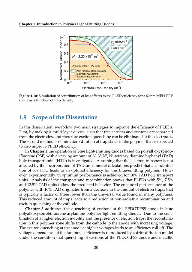
maximum value at about 1022m−3 trapping density. Further decrement of trapping den-sity does not enhance the efficiency. Exciton quenching amounts to typically 20% whenthe trapping density is high, and decreases to 10% for balanced transport when the trapdensity is too low. Then a symmetric recombination profile will be formed throughoutthe emissive layer, where each electrode contributes to half (5%) of the total quenchinglosses.
The trapping density for conjugated polymers has been reported to be about 3 ×10²³m−3. Here, it is found to be 2.1 × 10²³m−3 for MEH-PPV and indicated by a redarrow in the Figure 1.10. Elimination of traps can have a huge effect on the device effi-ciency. The blue arrow in the figure demonstrate that a ten times reduction of traps inthe polymer will increase the efficiency of a PLED more than 2 times. Since the trappingstate density is about 0.1% of transporting sites, identification and elimination of traps isa big dilemma that is costly and time consuming. For extrinsic defects purification mightbe the way to reduce electron trapping effects. If the trap states originate from structuraldefects like kinks in the polymer chain purification of the polymer will not lead to anyimprovement. As an alternative solution, we present in this thesis that it is possible tosimultaneously dilute trap states and transport sites.
19
Chapter 1. Introduction to Polymer Light-Emitting Diodes
Figure 1.10: Simulation of contribution of loss effects to the PLED efficiency for a 60 nm MEH-PPVdiode as a function of trap density
1.9 Scope of the Dissertation
In this dissertation, we follow two main strategies to improve the efficiency of PLEDs.First, by making a multi-layer device, such that free carriers and excitons are separatedfrom the electrodes, and therefore exciton quenching can be eliminated at the electrodes.The second method is elimination/dilution of trap states in the polymer that is expectedto also improve PLED efficiency.
In Chapter 2 the operation of blue light-emitting diodes based on polyalkoxyspirob-ifluorene (PSF) with a varying amount of N, N, N′, N′-tetraaryldiamino biphenyl (TAD)hole transport units (HTU) is investigated. Assuming that the electron transport is notaffected by the incorporation of TAD units model calculations predict that a concentra-tion of 5% HTU leads to an optimal efficiency for this blue-emitting polymer. How-ever, experimentally an optimum performance is achieved for 10% TAD hole transportunits. Analysis of the transport and recombination shows that PLEDs with 5%, 7.5%and 12.5% TAD units follow the predicted behavior. The enhanced performance of thepolymer with 10% TAD originates from a decrease in the amount of electron traps, thatis typically a factor of three lower than the universal value found in many polymers.This reduced amount of traps leads to a reduction of non-radiative recombination andexciton quenching at the cathode.
Chapter 3 addresses the quenching of excitons at the PEDOT:PSS anode in bluepolyalkoxyspirobifluorene-arylamine polymer light-emitting diodes. Due to the com-bination of a higher electron mobility and the presence of electron traps, the recombina-tion in this polymer zone shifts from the cathode to the anode with increasing voltage.The exciton quenching at the anode at higher voltages leads to an efficiency roll-off. Thevoltage dependence of the luminous efficiency is reproduced by a drift-diffusion modelunder the condition that quenching of excitons at the PEDOT:PSS anode and metallic
20

1.9. Scope of the Dissertation
cathode are of equal strength. Experimentally, the efficiency roll-off at high voltages dueto anode quenching is eliminated by the use of an electron-blocking layer between theanode and the light-emitting polymer.
In Chapter 4, we use MEH-PPV as a model polymer and we use PFO as hole-blockinglayer (HBL) to eliminate quenching of excitons at the metallic cathode. We investigate awide range of single-layer and bilayer PLEDs with different thicknesses consisting of apoly[2-methoxy-5-(2’-ethylhexyloxy)-p-phenylene vinylene] (MEH-PPV) emitting layerand a 20 nm poly(9,9’-dioctylfluorene) (PFO) HBL. The highest efficiency for both single-layer and bilayer devices is achieved when the total polymer layer thickness is ∼90 nm.As a result, addition of an HBL to reduce cathode quenching is only effective when theluminescence enhancement due to microcavity effects in PLEDs is restored. The relativeefficiency enhancement in bilayer devices as compared to single-layer devices variesfrom 283% for a 30 nm active layer to 20% for a 250 nm device.
One of the biggest challenges in the field of PLEDs is to increase their stability andlifetime. The main reason for the fast degradation of such devices is the use of highly-reactive metals, such as barium or calcium, as electrode material. In Chapter 5, we re-port the fabrication of an efficient PLED while using an air-stable partially oxidized alu-minum (AlOx) cathode. Usually, the relatively high work function of aluminum ( −4.2eV) imposes a large barrier for injecting electrons into the LUMO of the emissive poly-mer, which is frequently situated between −2.2 and −3.0 eV below the vacuum level.Here, we used F8BT as hole-blocking layer, which has a LUMO level of −3.3 eV that islower than that of MEH-PPV, −2.9 eV. By partially oxidizing aluminum the work func-tion can be decreased to −3.7± 0.3 eV. The combination of F8BT as hole blocking layerand oxidized Aluminum leads to voltage independent efficiencies that are even slightlyhigher as have been achieved for MEH-PPV diodes with reactive Ba/Al cathodes.
Chapter 6 deals with one of the most challenging topics in the field of polymer light-emitting diodes. As discussed, presence of electron traps reduces the light-output andmost importantly the efficiency of the PLEDs. As shown in Equation 1.11 the current ina semiconductor containing traps is reduced by N/Nr
t , with N the amount of transportsites, Nt the amount of traps and r a number that depends on the energy distribution ofthe traps. For r > 1 the possibility opens that trapping effects can be nearly eliminatedwhen N and Nt are simultaneously reduced. Solution-processed conjugated polymersare an excellent model system to test this hypothesis, because they can be easily dilutedby blending them with a large band gap semiconductor. We demonstrate that in con-jugated polymer blends with 10% active semiconductor and 90% large band gap hostthe typical strong electron trapping can be effectively eliminated. As a result we wereable to fabricate polymer light-emitting diodes with balanced electron and hole trans-port and reduced non-radiative trap-assisted recombination, leading to a doubling oftheir efficiency at nearly ten times lower material costs.
Since blue emitting polymers are very important in that sense they can be used asbackbone for white light-emitting PLEDs, in Chapter 7 we tested the dilution method onone of the most used blue light-emitting polymers, PSF-TAD. As is common for manyconjugated polymers used in light-emitting diodes (PLEDs) the charge transport in PSF-
21

Chapter 1. Introduction to Polymer Light-Emitting Diodes
TAD is dominated by holes. Although the free electron mobility is an order of magni-tude higher than the hole mobility, the electron transport is strongly hindered by traps.By diluting PSF-TAD with the wide band gap polymer poly(9,9-di-n-octylfluorenyl-2,7-diyl) (PFO) the effect of electron trapping can be nearly eliminated. As a result, thetransport in the PSF-TAD:PFO blend becomes electron dominated. Due to the higherelectron mobility, polymer light-emitting diodes (PLEDs) made from these blends ex-hibit higher current and light-output as compared to hole-dominated PLEDs made frompristine PSF-TAD. The reduced amount of electron traps enhances their efficiency from 2cd/A for the hole dominated PLED to 5.3 cd/A for the electron-dominated blend PLED.
22
References Chapter 1
References
[1] C. K. Chiang, C. R. Fincher, Y. W. Park, A. J. Heeger, H. Shirakawa, E. J. Louis, S. C.Gau, and Alan G. MacDiarmid, Phys. Rev. Lett. 39, 1098 (1977).
[2] H. Spreitzer, H. Becker, E. Kluge, W. Kreuder, H. Schenk, R. Demandt, and H. Schoo,Adv. Mater. 10, 1340 (1998).
[3] D. Braun and a. J. Heeger, Appl. Phys. Lett. 58, 1982 (1991).
[4] D. Moses, Appl. Phys. Lett. 60, 3215 (1992).
[5] Q. Pei and Y. Yang, J. Am. Chem. Soc. 118, 7416 (1996).
[6] U. Scherf, D. Neher, ”Polyfluorenes”, Springer, Heidelberg (2009).
[7] N. F. Mott and R. W. Gurney, ”Electronic Processes in Ionic Crystals”,2nded. OxfordUniversity Press, Oxford, (1948).
[8] J. Frenkel, Phys. Rev. 54, 647 (1938).
[9] D. M. Pai, J. Chem. Phys. 52, 2285 (1970).
[10] W. D. Gill, J. Appl. Phys. 43, 5033 (1972).
[11] E.M. Conwell, Phys. Rev. 103, 51 (1956).
[12] N. F. Mott, Can. J. Phys. 1956, 34, 1356.
[13] A. Miller and E. Abrahams, Phys. Rev. 120, 745 (1960).
[14] H. Bassler, Phys. Stat. Sol 15, 15 (1993).
[15] Y. N. Gartstein and E. Conwell, Chem. Phys. Lett., 245, 351 (1995).
[16] C. Tanase, E. J. Meijer, P. W. M. Blom, and D. M. de Leeuw, Phys. Rev. Lett. 91,216601 (2003).
[17] C. D. Dimitrakopoulos, S. Purushothaman, J. Kymissis, A. Callegari, and J. M. Shaw,Science 283, 822 (1999).
[18] G. Horowitz, M. E. Hajlaoui, and R. Hajlaoui, J. Appl. Phys. 87, 4456 (2000).
[19] W. F. Pasveer, J. Cottaar, C. Tanase, R. Coehoorn, P. A. Bobbert, P. W. M. Blom, D.M. de Leeuw, and M. A. J. Michels, Phys. Rev. Lett. 94, 206601 (2005).
[20] H. T. Nicolai, M. Kuik, G. A. H. Wetzelaer, B. de Boer, C. Campbell, C. Risko, J.L.Bredas, and P. W. M. Blom, Nat. Mater. 11, 882 (2012).
23
Chapter 1. Introduction to Polymer Light-Emitting Diodes
[21] M. Kuik, G. A. H. Wetzelaer, H. T. Nicolai, N.I. Craciun, D.M. De Leeuw, and P. W.M. Blom, Adv. Mater. 26, 512 (2014).
[22] M. A. Lampert, Phys. Rev. 103, 1648 (1956).
[23] M. Kuik, J. Vandenbergh, L. Goris, E.J. Begemann, L. Lutsen, D. J. M. Vanderzande,J. V. Manca, and P. W. M. Blom, Appl. Phys. Lett. 99, 183305 (2011).
[24] P. W. M. Blom, M. J. M. de Jong, and S. Breedijk, Appl. Phys. Lett. 71, 930 (1997).
[25] M. Kuik, L. J. A. Koster, G. A. H. Wetzelaer, and P. W. M. Blom, Phys. Rev. Lett. 107,256805 (2011).
[26] G. A. H. Wetzelaer, M. Kuik, H. T. Nicolai, and P. W. M. Blom, Phys. Rev. B 83,165204 (2011).
[27] M. Kuik, H. T. Nicolai, M. Lenes, G. A. H. Wetzelaer, M. Lu, and P. W. M. Blom,Appl. Phys. Lett. 98, 093301 (2011).
[28] D. E. Markov, J. C. Hummelen, and P. W. M. Blom, Phys. Rev. B 72, 045216 (2005).
[29] M. Kuik, L. J. A. Koster, G. Dijkstra, G. A. H. Wetzelaer, and P. W. M. Blom, Org.Electron. 13, 969 (2012).
[30] R. R. Chance, J. Chem. Phys. 62, 2245 (1975).
[31] D. Abbaszadeh, H.T. Nicolai, N.I. Craciun, and P. W. M. Blom, Phys. Rev. B 90,205204 (2014).
24