Embed Size (px)
Citation preview

UNIVERSITY OF NAIROBI
SCHOOL OF ENGINEERING
DEPT. OF ELECTRICAL AND INFORMATION
ENGINEERING
PROJECT REPORT
SPEED CONTROL OF A PERMANENT MAGNET
DC MOTOR USING DSP
PRJ 147
NAME: Kihika Lazarus Waweru
ADM NO: F17/1435/2011
PROJECT SUPERVISOR: MR. AHMED SAYYID
EXAMINER: DR. KAMUCHA
A Project Submitted in Partial Fulfillment of the Requirements for the
Award of the Degree in B.Sc. Electrical and Electronics Engineering
Submitted on: 13th May, 2016

i
Table of Contents Declaration of Originality ............................................................................................................... iii
Dedication ....................................................................................................................................... iv
Acknowledgement ............................................................................................................................ iv
List of Figures ..................................................................................................................................v
List of Tables ................................................................................................................................... vi
List of Abbreviations ....................................................................................................................... vi
Abstract .......................................................................................................................................... vii
CHAPTER ONE: INTRODUCTION ......................................................................................... 1
1.1 Problem Statement ...................................................................................................................1
1.2 Project Objectives .....................................................................................................................1
1.3 Project Scope ............................................................................................................................1
1.4 Project Organization ..................................................................................................................1
CHAPTER TWO: LITERATURE REVIEW ............................................................................ 2
2.10 DC MOTORS ............................................................................................................................2
2.11 PRINCIPLE OF OPERATION OF A PERMANENT MAGNET DC MOTOR ........................................2
2.12 SPEED OF A DC MOTOR ........................................................................................................3
2.13 SPEED CONTROL OF DC MOTOR USING DSP...........................................................................5
2.14 EQUIVALENT CIRCUIT OF A DC MOTOR..................................................................................5
2.15 FOUR QUADRANT OPERATION OF A DC MOTOR ....................................................................6
2.16 ADJUSTABLE SPEED DRIVES ..................................................................................................8
2.17 CONTROL OF ADJUSTABLE SPEED DRIVES ..............................................................................9
2.17 THE TRANSFER FUNCTION OF A PERMANENT MAGNET DC MOTOR ........................................9
2.2 DC – DC CONVERTERS .............................................................................................................. 10
2.21 THE BUCK CONVERTER ....................................................................................................... 11
2.22 CONTINUOUS CONDUCTION MODE .................................................................................... 13
2.3 PULSE WIDTH MODULATION (PWM) ........................................................................................ 14
2.4 DIGITAL SIGNAL PROCESSOR (DSP) ........................................................................................... 16
CHAPTER THREE: DESIGN ................................................................................................... 17
3.1 SPEED DRIVE REQUIREMENTS .................................................................................................. 17
3.2 DIGITAL SIGNAL PROCESSOR .................................................................................................... 17

ii
3.3 PERMANENT MAGNET DC MOTOR ........................................................................................... 20
3.4 MOSFET SWITCH ..................................................................................................................... 20
3.5 GATE DRIVE DESIGN ................................................................................................................ 21
3.6 COMPENSATOR DESIGN........................................................................................................... 22
CHAPTER THREE: SIMULATION ........................................................................................ 26
4.1 OPEN LOOP SIMUL ATION ........................................................................................................ 26
4.2 CLOSED LOOP SIMULATION ..................................................................................................... 26
CHAPTER FIVE: RESULTS & ANALYSIS ........................................................................... 28
5.1: DC MOTOR PRACTICAL RESULTS.............................................................................................. 28
5.2: OPEN LOOP SIMULATION RESULTS .......................................................................................... 29
5.3: CLOSED LOOP SIMULATION RESULTS ....................................................................................... 30
5.4: GATE DRIVE CIRCUIT RESULTS ................................................................................................. 30
CHAPTER SIX: CONCLUSION & RECOMMENDATION ................................................ 31
6.1: CONCLUSIONS........................................................................................................................ 31
6.2: DIFFICULTIES EXPERIENCED..................................................................................................... 31
6.3: RECOMMENDATION ............................................................................................................... 31
REFERENCES ................................................................................................................................... I
APPENDIX ..................................................................................................................................... II

iii
Declaration of Originality Name of Student:
Kihika Lazarus Waweru
Registration Number:
F17/1435/2011
College:
Architecture and Engineering
Faculty/School:
Engineering
Department:
Electrical and Information
Course Name:
Electrical and Electronics
Title of Work:
Speed Control of a Permanent DC Motor using DSP
1. I understand what plagiarism is and I am aware of the university policy in this regard.
2. I declare that this final year project report is my original work and has not been
submitted elsewhere for examination, award of a degree or publication. Where other
people’s work or my own work has been used, this has properly been acknowledged
and referenced in accordance with the University of Nairobi’s requirements.
3. I have not sought or used the services of any professional agencies to produce this work.
4. I have not allowed, and shall not allow anyone to copy my work with the intention of
passing it off as his/her own work.
5. I understand that any false claim in respect of this work shall result in disciplinary action,
in accordance with University anti-plagiarism policy.
SIGNATURE:
………………………………………………………………………………………
DATE: ………………………………………………………………

iv
Dedication I dedicate this project to my dear sister Carol and loving parents Paul and Muthoni Kihika for
their continued support throughout my course. I am forever indebted to you.
Acknowledgement Who can tell all the good things that the Lord has done? Who can praise Him enough? I
thank the Almighty God for His goodness and love. The far I have come and the far I am
to go, I praise Him.
I acknowledge my project supervisor Mr. Ahmed Sayyid. I would like to take this
opportunity to express my sincere gratitude to him for the support and guidance he has
provided during the entire period I have been working on the project. I am grateful for
the patience and zeal he has shown. I am highly indebted to him for giving me a better
understanding of the subject and valuable inputs.
I am grateful to Prof. Ouma A. H., the Chairman to the Department of Electrical and
Information Engineering, University of Nairobi for allowing me access to the
department’s equipment and for enabling me get the necessary components for the
completion of this project.
I would like to thank the Department laboratory assistants particularly Mr. Ng’ang’a and
Mr. Kimani in the Machines and Measurements lab respectively. Their support and
assistance throughout the time I’ve been doing tests for my project are highly
appreciated.
I would like to thank my friends for their support and criticism during my project period.
They have been my consistent anchors during this project.
Lastly, I would like to thank my parents and family members for their support and
encouragement as I carried out the project. They have been there for me and have always
been proud of me.
May the Almighty God bless, reward and be with you all.

v
List of Figures Fig 2.11: Principle of Operation of Permanent Magnet dc motor ……………………………pg 3
Fig 2.12: Dc motor Equivalent Circuit ………………………………………………………pg 6
Fig 2.13: Four Quadrant Operation of Dc motor …………………………………………….pg 7
Fig 2.14: Two Quadrant Converter ……………………….………………………………….pg 8
Fig 2.15: Single Quadrant Converter ………………………………………………………...pg 8
Fig 2.16: Closed loop Operation of Dc motor ……………………………………………….pg 9
Fig 2.17: Dc motor Transfer Function blocks ……………………………………………….pg 10
Fig 2.21: Dc – Dc Regulation Functional blocks ……………………………………………pg 11
Fig 2.22: Basic Dc – Dc Converter ……………………………………………………….....pg 11
Fig 2.23: Basic dc Converter Output ………………………………………………………..pg 12
Fig 2.24: Practical Dc – Dc Converter Circuit ……………………………………………....pg 13
Fig 2.25: Continuous Conduction Mode …………………………………………………….pg 14
Fig 2.31: Pulse Width Modulation signal Waveform ……………………………………….pg 15
Fig 2.32: 25% PWM signal Waveform ……………………………………………………...pg 15
Fig 3.11: Dc motor Speed control using DSP Flowchart ……………………………………pg 17
Fig 3.21: C2000 Piccolo Launchpad TMS320FX28027 ……………………………………pg 20
Fig 3.51: Schematic PCB for Gate Drive Circuit …………………………………………...pg 21
Fig 3.52: Express PCB Diagram for Gate Drive Circuit ……………………………………pg 22
Fig 3.61: Bode plot for Uncompensated motor System .........................................................pg 24
Fig 3.62: Step Response for Uncompensated motor System ……………………………….pg 24
Fig 3.63: Bode plot for the Compensated motor System …………………………………...pg 25
Fig 3.64: Step Response for the Compensated motor System ……………………………...pg 25
Fig 4.11: PSIM Open loop motor Simulation Circuit ……………………………………....pg 26
Fig 4.21: PSIM Closed loop motor Simulation Circuit …………………………………….pg 27
Fig 5.11: Tach-generator Output voltage against Speed graph …………………………….pg 29
Fig 5.41: Auto-coupler Gate Drive input and output waveforms ……………….………….pg 30

vi
List of Tables Table 5.11: Dc Motor Practical Results ……………………..…………….pg 28
Table 5.21: Dc Motor Open Loop Simulation Results …………………….pg 29
Table 5.31: Dc Motor Closed Loop Simulation Results …………………...pg 30
List of Abbreviations DSP Digital Signal Processing
DC Direct Current
AC Alternating Current
PWM Pulse Width Modulation
RPM Revolutions per minute
KVL Kirchoff’s Voltage Law
KCL Kirchorff’s Current Law
ADC Analogue to Digital Converter
GPIO General Purpose Input/Output

vii
Abstract Many industrial applications in the modern world such as conveyor belts, automobiles,
elevators, steel rolling mills, cranes, high precision digital tools, air conditioners and
robotics all involve rotation of dc motors at different speeds. Their simple nature,
precision and wide range speed control characteristics of dc motors make them most
suited in many applications. The subject of speed control in dc motors is hence very
critical for control engineers.
This project is about controlling the speed of a permanent magnet dc motor. A DSP is
used as the digital controller in this case. It generates PWM signals that correspond to the
desired speed. The PWM signals are then used to switch ON and OFF a MOSFET switch
hence controlling the power fed to the motor thus the speed. A closed loop system is to
be built by obtaining the output speed using a tacho-generator as the feedback. A closed
loop transfer function is also obtained for the system.
Simulation is done in both the open loop and closed loop system. Results of the simulations and
the practical results are obtained and compared and analyze

1
CHAPTER ONE: INTRODUCTION 1.1 Problem Statement
Speed control of DC motors is an inevitable topic in millions of industrial of applications. This
project is concerned with application of digital signal processing methods in realizing the speed
control of permanent magnet dc motors.
1.2 Project Objectives
Design of DC-DC converters
Modelling, simulating and construction of the dc motor control system
1.3 Project Scope
Demonstration of speed control of permanent magnet dc motor using a digital signal processor.
1.4 Project Organization Chapter one gives an introduction to the project; stating the project statement, objectives
and scope.
Chapter two gives the literature review of dc motors, dc-dc converters and digital signal
processors.
Chapter three gives the design analysis; looking into the speed drives, permanent magnet
dc motor speed requirements and analysis. The MOSFET switch is also investigated as
well as the gate drive circuit between the MOSFET and the DSP. The chapter is
concluded by the design of the motor controller compensator.
Chapter four gives the simulation of both open and closed loop simulations of the motor
speed control system in PSIM.
Chapter five presents the results for the open and closed loop simulations as well as for
motor practical results.
Chapter six represents a summary of the entire project, gives the conclusion and
recommendations on the same.

2
CHAPTER TWO: LITERATURE REVIEW
2.10 DC MOTORS
DC motors are devices that convert dc electrical energy to mechanical energy. A motor
works on the principle that a current-carrying conductor placed in a magnetic field experiences a
force. This force is due to the interaction between magnetic field due to the current carrying
conductor and the magnetic field that existed. A motor can derive its electrical energy from
either a dc source or from an AC source. They can therefore be referred to as either dc motors or
ac motors. The magnetic field of the motors can be derived from either a permanent magnet or
from an electromagnet.
The three basic types of DC motors are the series motor, the shunt motor, and the
compound motor.
The series motor is designed to move large loads with high starting torque in
applications such as a crane motor or lift hoist.
The shunt motor is designed slightly differently, since it is made for applications
such as pumping fluids, where constant-speed characteristics are important.
The compound motor is designed with some of the series motor's characteristics
and some of the shunt motor's characteristics. This allows the compound motor to
be used in applications where high starting torque and controlled operating speed
are both required.
2.11 PRINCIPLE OF OPERATION OF A PERMANENT MAGNET DC MOTOR A rectangular coil free to rotate about a fixed axis is placed inside a magnetic field produced by a
permanent magnet as shown in figure 1.10 below. A dc current is fed into the coil through
carbon brushes bearing on a commutator, which consists of a metal ring split into two halves
separated by insulation. As current flows through the coil a magnetic field is set up around the
coil which interacts with the magnetic field due to the permanent magnet. This causes a force F
to be exerted on the conductor, whose direction can be determined by the Fleming’s Left hand
rule. This causes a torque and the coil rotates. When the coil has rotated through 900 the negative
and positive terminals of the supply interchange the commutator halves thus, reversing the
current direction. This prevents the coil from rotating in the opposite direction, thus it rotates
continuously in one direction.

3
Fig. 2.11
2.12 SPEED OF A DC MOTOR BACK EMF, Eb.
When the armature of a dc motor rotates under the influence of the driving torque, the
armature conductor moves through the magnetic field due to the permanent magnet, thus an emf
is induced in them as in a generator. The induced emf acts in opposite direction to the direction
of the applied voltage, Vt (Lenz’s Law). The induced emf is known as back emf or counter emf,
Eb. The back emf is given by;
Eb = 𝑃∅𝑍𝑁
60𝐴 (Eqn 2.10).
Where,
P= Number of poles of the permanent magnet,
∅= Flux per pole in Wb,
Z= total number of armature conductors,
N= speed of the motor in rpm
A= number of parallel paths;
(A=2 for simplex wave winding, A=P for simplex lap winding)
The back emf is always smaller than the applied voltage, although the difference is small
when the motor is running under normal conditions.
From the motor equation given by;
Vt = Eb + IaRa (Eqn 2.11).

4
Then the net voltage across the armature circuit is,
Va = Vt − Eb (Eqn 2.12).
And the back emf will be given by;
Eb = Vt − IaRa (Eqn 2.13).
Since Vt and Ra are usually fixed, the value of Eb determines the current Ia drawn by the motor. If
the speed N of the motor is high, then Eb is large from Eqn 2.1 hence the motor draws less
armature current and vice versa.
Thus, from Eqn 1.11 and 1.13 we obtain
𝑃∅𝑍𝑁
60𝐴= 𝑉𝑡 – 𝐼𝑎𝑅𝑎 (Eqn 2.14)
N = (Vt – IaRa) 60A
∅PZ (Eqn 2.15)
N = K (Vt – IaRa)
∅ (Eqn 2.16)
Where
K = 60A
PZ
Armature torque is given by;
𝑇 =𝑍∅𝐼𝑎𝑃
2𝜋𝐴=
𝐼𝑎𝐸𝑏
𝜔𝑎 (Eqn 2.18)
Where 𝜔a = 2𝜋N is the angular velocity of the motor shaft
There are three main methods of controlling the speed of a dc motor, namely:
i. By varying the flux per pole (∅). This is called flux control method.
ii. By varying the resistance in the armature circuit. This is called armature control method
iii. By varying the applied voltage. This is called voltage control method.
But the above methods suffer from several disadvantages, which include:
Low efficiency at low speeds and hence low charge cycle for the battery.

5
Speed can be controlled only below base speed.
Battery voltage variations cannot be compensated.
Limited to brushed DC motors only.
2.13 SPEED CONTROL OF DC MOTOR USING DSP Digital Signal processing technology is enabling cost effective and energy efficient
control system design. The performance of a DSP architecture allows an intelligent approach to
reduce the complete system costs. PWM switching control methods improve speed control and
reduce the power losses in the system, which increases the mean time between charge cycles of
the battery. The reduced losses also help to reduce the weight of the system. In PWM control
methods, appropriate circuit and control methods allow speeds above base speed to be achieved.
Moreover using gate drive IC’s improve the ruggedness and reliability of the system.
2.14 EQUIVALENT CIRCUIT OF A DC MOTOR In a dc motor, the field flux ∅f is established by the stator, either by means of a
permanent magnet where the field flux ∅f remains constant or by means of a field winding where
the field current If controls the flux ∅f. The rotor carries in its slots the armature winding, which
handles the electrical power. The interaction of the field flux ∅f and the armature current Ia
produces the electromagnetic torque;
Tem = kt∅fIa (Eqn 2.20)
Where kt is the torque constant of the motor.
A back emf is produced in the armature circuit by the rotation of the armature conductors of a
speed 𝜔m in the presence of a field flux ∅f:
ea = ke∅f𝜔m
where ke is the voltage constant of the dc motor.
The interaction between Tem with the load torque determines how the motor speed builds up.
𝑇𝑒𝑚 = 𝐽𝑑𝜔𝑚
𝑑𝑡 + 𝐵ωm + Tωl(t) (Eqn 2.21)

6
Where J and B are the total equivalent inertia and the damping respectively, of the motor-load
combination and T𝜔L is the equivalent working torque of the load.
Fig 2.12
A controllable voltage source Vt is applied to the armature terminals to establish Ia. Thus
the armature current is determined by Vt, the induced emf ea, the armature resistance Ra, and the
armature winding inductance La.
Vt = ea + RaIa + La𝑑𝐼𝑎
𝑑𝑡 (Eqn 2.23)
2.15 FOUR QUADRANT OPERATION OF A DC MOTOR DC machines act as generators while braking. To consider braking, it’s assumed that the
flux ∅f is kept constant and the motor is initially driving a load at speed 𝜔m. To reduce speed,
the armature voltage Vt is reduced below ea so that the armature current Ia reverses in direction.
The electromagnetic torque Tem reverses in direction and the kinetic energy associated with the
motor load inertia is converted into electrical energy by the dc machine. This energy must
somehow be absorbed by the source Vt or be dissipated by a resistor.

7
During braking operation, the polarity of ea does not change since the direction of
rotation has not changed. As the rotor slows down, ea decreases in magnitude. The generation
stops when the rotor comes to a standstill and all the inertial energy has been exhausted. The
direction of rotation of the motor is reversed by reversing the polarity of the terminal voltage Vt.
A dc motor can therefore operate in either direction and its electromagnetic torque can be
reversed for braking, as shown by the four quadrants of the torque-speed plane in figure below.
Fig 2.13
In permanent magnet dc motors, permanent magnets on the stator produce a constant field flux
∅f and thus we have;
Tem = kTIa (Eqn 2.30)
Ea = kE𝜔m (Eqn 2.31)
Vt = Ea + RaIa (Eqn 2.32)
The steady state speed can thus be obtained as a function of Tem for a given value of Vt.
𝜔m = 1
kE(𝑉𝑡 −
Ra
kT 𝑇𝑒𝑚) (Eqn 2.33)

8
The speed of a load with an arbitrary torque-speed characteristics can hence be controlled by
controlling Vt in a permanent magnet dc motor.
2.16 ADJUSTABLE SPEED DRIVES A switch mode dc-dc converter can be used to control the speed of a dc motor. Figure 2.14 is a
two quadrant converter which can be used when reversing the direction of the motor rotation is
not needed but braking is required.
Fig 2.14
For a single quadrant operation where speed is to remain unidirectional and there is no need for
braking, the step down converter of figure 2.15 can be used.
Fig 2.15

9
2.17 CONTROL OF ADJUSTABLE SPEED DRIVES Figure 2.16 shows a block diagram of a dc motor operating in closed loop to deliver
controlled speed. The speed transducer converts the mechanical energy (speed) into an electrical
signal. The electrical signal is fed to the controller as a feedback. The controller compares the
feedback signal to the reference signal (speed) and produces a PWM signal of appropriate duty
cycle. The PWM signal is used to control the switch of the power electronics converter. This
controls the terminal voltage Vt and hence, the speed.
Ref speed
Fig 2.16
2.17 THE TRANSFER FUNCTION OF A PERMANENT MAGNET DC MOTOR
The following equations written in terms of small deviations around their steady
state values are used for analyzing small signal performance of the motor-load
combination around a steady state operating point.
Δvt = Δea + RaΔia
Δea = kE Δ𝜔m
ΔTem = kT Δia
ΔTem = ΔTWL
Taking the Laplace transforms of these equations;
Vt(s) = Ea(s) + (Ra + sLa) Ia(s)
Ea(s) = kE𝜔m(s)
Tem(s) = kTIa(s)
Tem(s) = TWL(S) + (B + sJ) 𝜔m(s)
Speed
Controler
Power
Electronics
motor drive
Motor Load
Speed
Transducer Motor speed (Voltage signal)

10
𝜔m(s) = sθm(s)
These equations for the motor-load combination can be represented by the transfer function
blocks as shown in figure 2.7.
Fig 2.17
The inputs to the motor-load combination in the figure are the armature voltage Vt(s) and
the load torque TWL(s). Applying one input at a time and setting the other input to zero,
the superposition principle yields;
This equation results in two closed loop transfer functions:
G1(s)
with Twl(s) = 0 and
G2(s)
with Vt(s) = 0
2.2 DC – DC CONVERTERS DC-DC converters are used to convert unregulated dc input voltage to a controlled dc output
voltage at a desired level.
The unregulated dc input voltage can be obtained by rectifying the line voltage or from a dc
source such as a battery, as shown in figure 2.70.

11
Fig 2.21
AC line voltage
1-phase or 3-phase
There are several types of dc-dc converters. The following are some of the types of dc-dc
converters that exist:
i. Step-down (buck) converter
ii. Step-up (boost) converter
iii. Step-down/step-up converter (buck-boost) converter
iv. Buck converter
v. Full bridge converter
In this project the buck converter is discussed and used.
2.21 THE BUCK CONVERTER The average dc output voltage of a dc-dc converter is controlled to equal a desired level,
even though the input dc voltage and the output load may fluctuate. The average output voltage
is controlled by controlling the switch “on” and “off” durations (ton and toff). Figure 2.8
illustrates a basic dc-dc converter.
Fig 2.22

12
The average value Vo of the output voltage vo depends on ton and toff as shown in figure 2.71
below.
Fig 2.23
The output voltage is controlled by switching at a constant frequency (and hence a constant
switching time period Ts = ton + toff). The duty ratio, D is defined as the ratio of the on duration
to the switching time period. Adjusting the on duration therefore, varies the duty ratio, D.
𝐷 = 𝑡𝑜𝑛
𝑇𝑠 (Eqn 2.70)
The basic circuit of figure 2.70 constitutes a buck converter for purely resistive load. Assuming
an ideal switch, a constant instantaneous input voltage Vd and a purely resistive load, the
instantaneous output voltage waveform is shown in figure 2.71 as a function of the switch
position. The average output voltage can be calculated in terms of the switch duty ratio, D:
(Eqn 2.71)
= 𝑡𝑜𝑛
𝑇𝑠Vd (Eqn 2.72)
= DVd (Eqn 2.73)
Varying the duty ratio, D thus, controls the output voltage Vo.
The circuit of figure 2.70 above has two drawbacks:
i. In practice, the load would be inductive and even with resistive loads there would
always be stray inductance. The switch will thus absorb (or dissipate) the inductive
energy and may be destroyed.

13
ii. The output voltage fluctuates between Vd and zero, which is not acceptable for most
applications.
The circuit of figure 2.24 below is used to overcome these drawbacks.
Fig 2.24
The problem of stored inductive energy is overcome by using a diode as shown in the
figure above. A low pass filter consisting of an inductor and a capacitor is used to diminish the
output voltage fluctuations. The corner frequency of the low pass filter is chosen to much lower
than the switching frequency fs, thus eliminating the switching ripple in the output voltage.
When the switch is on, the diode becomes reversed biased and input provides energy to the load
and the inductor. When the switch is off the inductor current flows through the diode,
transferring some of its stored energy to the load. The average inductor current is equal to the
average output current Io, since the average capacitor current in steady state is zero.
2.22 CONTINUOUS CONDUCTION MODE In continuous conduction of operation, the inductor current flows continuously and does
not fall to zero. The figure below shows the waveforms of continuous conduction mode.
When the switch is on, it conducts the inductor current and the diode becomes reverse biased.
This results in a positive voltage VL = Vd + Vo, across the inductor. This voltage causes linear
increase in inductor current IL. When the switch is turned off, the inductive energy causes IL to
continue flowing. The current now flows through the diode and Vo = -VL.

14
Fig 2.25
Since in steady state operation the waveform must repeat from one time period to the next;
(Eqn 2.74)
Therefore;
(𝑉𝑑 − 𝑉𝑜)𝑡𝑜𝑛 = (𝑇𝑠 − 𝑡𝑜𝑛) (Eqn 2.75)
Or,
(Eqn 2.76)
The output voltage is thus proportional to the value of the duty cycle, D as shown in the equation
above. In discontinuous conduction mode the inductor current goes to zero during the period
when the switch is off and it does not flow until when the switch is turned on again.
2.3 PULSE WIDTH MODULATION (PWM) A Pulse refers to an electromagnetic wave or modulation thereof of brief duration while
Width Modulation is to adjust to proper measure or proportion the width of the pulse with
respect to the frequency of the wave. Pulse Width Modulation (PWM) is therefore a way of
delivering energy through a succession of pulses rather than a continuously varying analog
signal. We consider the waveform in the figure below;

15
Fig 2.31
The signal is a voltage switching between 12V and 0V. A device connected to use the signal will
see the average voltage. Since the time the signal is 12V is equal to the time the signal is 0V in
the figure shown above, an average voltage of 6V will be seen by the device. The positive pulse
lasts for 50% of the total time.
In the figure 1.92 below, the positive pulse only lasts for 25% of the total time. The average
voltage seen by the device in this case is 3V, that is, less than in the first case. The voltage is
equivalent to the product of the positive pulse value and 25%.
Fig 2.32
Varying the time of the positive pulse thus varies the average output voltage. The percentage of
the time of positive pulse compared to the period of the signal is called the duty cycle, D of the
signal. In the figures above the duty cycle, D was therefore, 50% and 25% respectively.
PWM signals have the advantage of high efficiency compared to other signals. They
however, cannot be used by some devices due to their abrupt and periodic changes in magnitude.
Several circuits can be used to generate PWM signals. A digital signal processor (DSP) is
normally programmed to produce PWM signals.

16
APPLICATIONS OF THE PWM
A suitable device has to be used to see the average output voltage, since some devices
don’t work properly with abrupt changing voltages. Pulse width modulated signals are used to
control the speed of a motor, as control voltages for switches, hence greatly used in power
electronics converters among others.
2.4 DIGITAL SIGNAL PROCESSOR (DSP) A digital signal processor (DSP) is a specialized microprocessor, with its architecture
optimized for the operational needs of digital signal processing. The goal of DSPs is usually to
measure, filter and/or compress continuous real-world analog signals. Most general-purpose
microprocessors can also execute digital signal processing algorithms successfully, but dedicated
DSPs usually have better power efficiency. Thus, they are more suitable in portable devices such
as mobile phones because of power consumption constraints. DSPs often use special memory
architectures that are able to fetch multiple data and/or instructions at the same time.
Digital Signal Processing both provides a mathematical description of the systems to be
designed and also implements them (either by software programming or by hardware
embedding) without much dependency on hardware issues, which explains the importance and
success of DSP engineering.
DSP processor ICs are found in every type of modern electronic systems and products
including, SDTV | HDTV sets, radios and mobile communication devices, Hi-Fi audio
equipment, Dolby noise reduction algorithms, GSM mobile phones, mp3 multimedia players,
camcorders and digital cameras, automobile control systems, noise cancelling headphones,
digital spectrum analyzers, intelligent missile guidance, radar, GPS based cruise control systems
and all kinds of image processing, video processing, audio processing and speech processing
systems.
The DSPs have the following advantages when used as controllers over the other
controllers:
Low cost
High performance
Flexibility of quick design modifications
Implementation of more control schemes
Less susceptible to aging, environmental variations & have better noise immunity.

17
CHAPTER THREE: DESIGN
This project requires that the speed of a permanent magnet dc motor is digitally controlled using
a DSP microcontroller. A feedback system for the speed control system is to be provided. A
tacho-generator is to be used as a device that converts the output speed to a voltage signal that is
fed back to the DSP to make a closed loop control system.
3.1 SPEED DRIVE REQUIREMENTS Different components are used in the design of the speed control system. These include a
permanent magnet dc motor, a tacho-generator, DSP, MOSFET switch and its gate drive. The
flow chart of figure 3.11 below shows how the different components interoperated to complete
the project:
Fig 3.11
3.2 DIGITAL SIGNAL PROCESSOR A DSP is used as the digital controller in this project. The controller is to be designed in
analog using MATLAB and implemented using a DSP.
The DSP used is a TMS320F28027 from Texas Instruments. This is a member of the F2802x
Piccolo family of microcontrollers. This family of microcontrollers provides the power of the

18
C28x core coupled with highly integrated control peripherals in low pin-count devices. Features
of the TMS320F28027 are:
High-Efficiency 32-Bit CPU (TMS320C28x)
60 MHz (16.67-ns Cycle Time)
50 MHz (20-ns Cycle Time)
40 MHz (25-ns Cycle Time)
16 x 16 and 32 x 32 MAC Operations
16 x 16 Dual MAC
Harvard Bus Architecture
Atomic Operations
Fast Interrupt Response and Processing
Unified Memory Programming Model
Code-Efficient (in C/C++ and Assembly)
Endianness: Little Endian
Low Cost for Both Device and System:
Single 3.3-V Supply
No Power Sequencing Requirement
Integrated Power-on and Brown-out Resets
Small Packaging, as Low as 38-Pin Available
Low Power
No Analog Support Pins
Clocking:
Two Internal Zero-pin Oscillators
On-Chip Crystal Oscillator/External Clock Input
Dynamic PLL Ratio Changes Supported
Watchdog Timer Module
Missing Clock Detection Circuitry
Up to 22 Individually Programmable, Multiplexed GPIO Pins With Input Filtering
Peripheral Interrupt Expansion (PIE) Block That Supports All Peripheral Interrupts
Three 32-Bit CPU Timers
Independent 16-Bit Timer in Each ePWM Module

19
On-Chip Memory
Flash, SARAM, OTP, Boot ROM Available
Code-Security Module
128-Bit Security Key/Lock
Protects Secure Memory Blocks
Prevents Firmware Reverse Engineering
Serial Port Peripherals
One SCI (UART) Module
One SPI Module
One Inter-Integrated-Circuit (I2C) Bus
Enhanced Control Peripherals
Enhanced Pulse Width Modulator (ePWM)
High-Resolution PWM (HRPWM) Module
Enhanced Capture (eCAP) Module
Analog-to-Digital Converter (ADC)
On-Chip Temperature Sensor
Comparator
Advanced Emulation Features
Analysis and Breakpoint Functions
Real-Time Debug via Hardware
2802x, 2802xx Packages
38-Pin DA Thin Shrink Small-Outline Package (TSSOP)
48-Pin PT Low-Profile Quad Flatpack (LQFP)
The program used was designed on Code Composer Studio IDE and Control Suit both from
the Texas Instruments, which are compatible with the DSP. The figure 2.2 below shows a
photo of the TMS320F28027 C2000 Launchpad.

20
Fig 3.21
3.3 PERMANENT MAGNET DC MOTOR A 220V dc motor was used but operated at a maximum of 120V. The armature resistance was
calculated as the gradient of the graph of armature voltage against armature current. Different
values of armature current were recorded at different armature voltages as shown in table 1. A
graph of Armature voltage against Armature current was then drawn.
3.4 MOSFET SWITCH A MOSFET was used as the switch to the buck converter. The MOSFET used is to be controlled
by the PWM signals from the digital controller-the DSP. The MOSFET does not see the average
voltage of the PWM signal, but it sees HIGH voltages followed by LOW voltages repeatedly just
like the PWM signal appears, and at the same frequency as the frequency of the signal.
The MOSFET switches ON when a HIGH voltage is applied to its gate and OFF when a LOW
voltage is applied to gate. It therefore, switches ON and OFF at the frequency of the PWM
signal.
The MOSFET used had the following properties: 500V and 10A

21
3.5 GATE DRIVE DESIGN The switching time of a transistor needs to be kept as short as possible, to minimize
power losses. However, the switching time is inversely proportional to the amount of current
used to charge the gate. Switching currents are therefore required in terms of several hundreds of
mA or even Amperes.
The switching signal, which is a PWM signal, for the transistor is generated by a DSP. The DSP
provides an output signal that is limited to a few mA of current. Consequently, if the transistor is
directly driven by such a signal, it would switch very slowly, with correspondingly high power
loss. The gate capacitor of the transistor will draw current so quickly, during switching, that it
causes a current overdraw in the DSP, causing overheating which may lead to permanent
damage or even completely destroy DSP. A gate driver is thus provided between the DSP output
signal and the power transistor to prevent this from happening.
The gate drive circuit was realized using an isolated auto-coupler IC HCPL3120 shown
in PCB schematic figure 3.51 below. CN1 is the connector where the PWM signal from the DSP
is fed to the gate drive. CN2 is the connector to which power supply to the motor was fed, this is
the voltage being controlled in order to control the motor speed. Terminal 1 of CN3 was
connected to the gate of the MOSFET while terminal 2 to the source.
To determine the value of R1, the IF of the auto-coupler must be considered. Then R1 is
given by:
Since 7mA < IF < 16mA for HCPL3120
we select IF = 10mA
R1 = Vcc−1.4
I =
5−1.4
10𝑚𝐴 = 360Ω
Fig 3.51
22
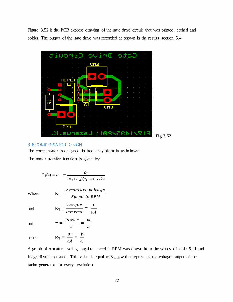
Figure 3.52 is the PCB express drawing of the gate drive circuit that was printed, etched and
solder. The output of the gate drive was recorded as shown in the results section 5.4.
Fig 3.52
3.6 COMPENSATOR DESIGN The compensator is designed in frequency domain as follows:
The motor transfer function is given by:
G1(s) = 𝜔
Where KE = 𝐴𝑟𝑚𝑎𝑡𝑢𝑟𝑒 𝑣𝑜𝑙𝑡𝑎𝑔𝑒
𝑆𝑝𝑒𝑒𝑑 𝑖𝑛 𝑅𝑃𝑀
and KT = 𝑇𝑜𝑟𝑞𝑢𝑒
𝑐𝑢𝑟𝑟𝑒𝑛𝑡 =
𝜏
𝜔𝑖
but 𝜏 = 𝑃𝑜𝑤𝑒𝑟
𝜔 =
𝑣𝑖
𝜔
hence KT = 𝑣𝑖
𝜔𝑖 =
𝑣
𝜔
A graph of Armature voltage against speed in RPM was drawn from the values of table 5.11 and
its gradient calculated. This value is equal to Ktach which represents the voltage output of the
tacho-generator for every revolution.

23
Ktach = 0.0194 V/rad/s
KT = 0.84302 V/rad/s
The motor inertia moment is provided in the datasheet and is given as;
J = 0.04 kgm3
B = 0.0019 N/rad/s
The values of Ra and La for the motor were determined by measurement.
Ra = 2.27 Ω
La = 0.018 H
The damping coefficient is so small and can be assumed negligible in the calculations. Hence,
the motor speed transfer equation G1(s) becomes:
G1(s) = 𝜔 = 0.84302
(0.04𝑠+0.0019)(0.018𝑠+2.27)+0.84302𝑥0.84302
= 0.84302
0.00072𝑠∗2+0.09114𝑠+0.71068
= 1170.86
𝑠∗2+126.58𝑠+987.55
= 51.56 5.109
𝑠∗2+1025𝑠+5.109
This transfer function was used to design the compensator in MATLAB as follows:
A new m-file was created and the following code written;
%Practical Motor System Equation
num = [1170.86] denom = [1 126.58 987.55]
Gp = tf(num, denom) bode (Gp) grid on title ('Step Response for Compensated motor') hold on
The bode plot and step response obtained for the uncompensated motor system is shown in the
figure below.

24
Fig 3.61
Fig 3.62
From the bode plot and step response for the motor, it was notes to have a phase margin of 91.10
and a long settling time of approximately 800s. To improve the phase margin and response for
the motor, a compensator was designed.
A PD controller with Kp = 100 and Kd = 5 was noted to improve the motor characteristics to give
a faster time response and a lower phase margin. The bode plot and step response of the
compensated system are shown below.

25
Fig 3.63
Fig 3.64
Below is the code added to the previous in order generate the above bode plot for the
compensated system.
%Compensted System
Kp = 100 Ki = 0 Kd = 5
Gc = pid(Kp, Ki, Kd) H = 1 Mc = feedback(Gp*Gc, H) bode (Mc) grid on

26
CHAPTER THREE: SIMULATION Simulation of the various circuits was done using the PowerSim software as follows in this
chapter sections.
4.1 OPEN LOOP SIMUL ATION The aim of this simulation was to obtain different values of speed at different duty cycles
hence armature voltages. The circuit was connected to match the speed of the practical motor
used at different armature voltages. The speed of the motor was recorded against various duty
cycles of the square wave voltage source driving the MOSFET as shown in table 5.21.
The circuit for the open loop simulation was as shown below:
Fig 4.11
4.2 CLOSED LOOP SIMULATION A feedback system was incorporated with the proportional compensator designed to form
a closed loop system. The compensator replaced the PWM producer in the open loop circuit.
The aim of this simulation was to get different values of speed using different values of the
reference voltage. A voltage of 2.4V was used as the maximum reference voltage and it was
reduced using a voltage divider to give different values for the reference voltage. The speed of
the motor was recorded against various positions of the rheostat. These positions represents the

27
reference speeds input to system. The difference between the reference speed and the actual
speed gives an error signal to the controller that in turn regulates the duty cycle of the signal fed
to the MOSFET. This ensures that the actual speed of the motor follows the reference speed. The
figure below shows the circuit of the closed loop simulation and the results obtained were
recorded as shown in table 5.31.
Fig 4.21

28
CHAPTER FIVE: RESULTS & ANALYSIS
5.1: DC MOTOR PRACTICAL RESULTS To be able to determine the various motor constants required for its modelling in designing the
controller, an experiment was carried out on the motor. The table below shows the parameters
and values obtained. A graph of tachogenerator output voltage against motor speed was then
plotted as shown in fig 4.11 and it’s slope is numerically equal to Ktach = 0.0194.
Table 5.11
Va Ia Vtach N(rpm) 𝜔 = 2𝜋*(rpm)/60 Ktach = Vtach/𝜔 KT = Va/𝜔
15 0.1 0.29 143 14.97 0.01937 1.002
32 0.2 0.7 344 36.02 0.01943 0.8884
37 0.2 0.83 408 42.73 0.01942 0.8805
42 0.2 0.94 459 48.07 0.01955 0.8737
48 0.2 1.03 538 56.34 0.01828 0.8519
59 0.2 1.36 666 69.74 0.0195 0.8460
66 0.2 1.53 753 78.85 0.0194 0.8370
71 0.3 1.66 813 85.14 0.01949 0.8339
81 0.3 1.89 929 97.28 0.0194 0.8326
92 0.3 2.14 1055 110.48 0.01937 0.8327
97 0.3 2.27 1119 117.18 0.01937 0.8277
103 0.3 2.41 1188 124.41 0.01937 0.8279
107 0.3 2.5 1230 128.81 0.01941 0.8307
117 0.3 2.75 1352 141.58 0.01942 0.8264
122 0.3 2.88 1415 148.18 0.01944 0.8233
0.0194 0.84302

29
Fig 5.11
5.2: OPEN LOOP SIMULATION RESULTS The figure 4.11 was created in PSIM with motor characteristics of set to match those of
the practical motor, that is, Ra = 1.2Ω, La = 8.2x10⁻³H, Nrated = 1200rpm, Ia(rated) = 1.6A and
Va(rated) = 120V. For different duty cycles of the clock, the speed obtained was recorded as shown
in Table 4.21 below;
Table 5.21
Duty cycle Motor speed, N (rpm)
0.05 42
0.15 168
0.25 294
0.35 419
0.45 545
0.50 608
0.65 797
0.75 923
0.85 1049
0.95 1175
0
0.5
1
1.5
2
2.5
3
3.5
0 200 400 600 800 1000 1200 1400 1600
Vta
ch
speed
Graph of Output Voltage aginst Speed in rpm

30
5.3: CLOSED LOOP SIMULATION RESULTS Table 5.31
Rheostat position (Reference
speed)
Armature voltage, Va (V) Motor Speed, N (rpm)
0.1 18 172
0.2 26 228
0.3 35 343
0.4 44 478
0.5 57 596
0.6 63 702
0.7 71 887
0.8 85 950
0.9 98 1076
1.0 114 1194
5.4: GATE DRIVE CIRCUIT RESULTS The input and output of the auto-coupler gate drive circuit was viewed on the oscilloscope screen
and captured as shown in the figure 4.41 below.
Fig 5.41

31
CHAPTER SIX: CONCLUSION & RECOMMENDATION 6.1: CONCLUSIONS The importance of permanent magnet dc motor speed control cannot be overstated. This
project has shown that cheaper and simpler methods can be used to control the speed of a
permanent magnet dc motor efficiently and accurately.
In order for the digital control for the dc motor to be realized in this project, the motor
was first modelled. This involved obtaining its transfer function for the closed loop
system which helped determine the motor characteristics. A compensator that improves
the motor performance to the desired characteristics was then designed. The code was
then written for the DSP controller to effect the digital speed control for the permanent
magnet dc motor. The motor speed was converted to equivalent voltage value through a
tacho-generator. This voltage was fed back to the DSP through an ADC to provide a
feedback for the controller.
The DSP realizes this control through sending PWM signals to the gate of the MOSFET
that would in turn switch the power to the motor ON and OFF at high frequency. The
speed of the motor is hence directly related to the average power delivered to it through
the PWM signal which is dependent the duty cycle. The DSP output PWM signal is
limited to a few mA current. Consequently, if the transistor is directly driven by such a
signal, it would switch very slowly, with correspondingly high power loss. A gate driver
is thus provided between the DSP output signal and the power transistor to prevent this
from happening.
6.2: DIFFICULTIES EXPERIENCED The implementation of the closed loop for the motor was initially a challenge as well as
writing the code for the DSP.
6.3: RECOMMENDATION Designing and implementing the dc motor speed control drive in all the four
quadrants. This will be able to give rotation in either direction and provide
braking for the dc motor.
Using the microprocessor to detect and display the speed of the dc motor on a
screen

I
REFERENCES Power Electronics (Circuits, Devices and Applications), Muhammad H. Rashid
A. E. Fitzgerald, C. K. (2003). Electric Machinery. New York: McGraw-Hill.
Nice N. S. (1996). Control Systems Engineering. John Wiley & Sons Inc
Bishop, R. H. (n.d.). Mordern Control Systems Analysis. ADDISON WESLEY.
Analysis & Design of Analog Integrated Circuits 4ed -Grey, Hurst, Lewis, Meyer
Introduction to Microprocessors and Microcontrollers 2nd Ed.~tqw~_darksiderg
Ned Mohan, T. M. (2003). POWER ELECTRONICS. Jolm Wiley & Sons.
John Bird. (2003). Electrical and Electronic Principles and Technology. Newnes.
Robert W. Erickson. (2001). Fundanentals of Power Electronics. Kluwer Academic Publishers.
www.ti.com
http://www.Analogdevices.com
www.mathworks.com/controltutorials

II
APPENDIX
//----------------------------------------------------------------------------------
// FILE: ProjectName-Main.C
// Description: Sample Template file to edit
// The file drives duty on PWM1A using C28x
// These can be deleted and modifed by the user
// C28x ISR is triggered by the PWM 1 interrupt
// Version: 2.0
// Target: TMS320F2802x(PiccoloA),
// Copyright Texas Instruments © 2004-2010
// October 2010 - Sample template project with DPLib v3 (MB)
// PLEASE READ - Useful notes about this Project
// Although this project is made up of several files, the most important ones are:
// "ProjectName-Main.C" - this file
// - Application Initialization, Peripheral config,
// - Application management
// - Slower background code loops and Task scheduling
// "ProjectName-DevInit_F28xxx.C
// - Device Initialization, e.g. Clock, PLL, WD, GPIO mapping
// - Peripheral clock enables
// - DevInit file will differ per each F28xxx device series, e.g. F280x, F2833x,
// "ProjectName-DPL-ISR.asm
// - Assembly level library Macros and any cycle critical functions are found here
// "ProjectName-DPL-CLA.asm"
// - Init code for DPlib CLA Macros run by C28x
// - CLA Task code
// "ProjectName-Settings.h"
// - Global defines (settings) project selections are found here

III
// - This file is referenced by both C and ASM files.
// "ProjectName-CLAShared.h.h"
// - Variable defines and header includes that are shared b/w CLA and C28x
// Code is made up of sections, e.g. "FUNCTION PROTOTYPES", "VARIABLE
DECLARATIONS" ,..etc
// each section has FRAMEWORK and USER areas.
// FRAMEWORK areas provide useful ready made "infrastructure" code which for the most part
// does not need modification, e.g. Task scheduling, ISR call, GUI interface support,...etc
// USER areas have functional example code which can be modified by USER to fit their appl.
// Code can be compiled with various build options (Incremental Builds IBx), these
// options are selected in file "ProjectName-Settings.h". Note: "Rebuild All" compile
// tool bar button must be used if this file is modified.
//----------------------------------------------------------------------------------
#include "ProjectName-Settings.h"
#include "PeripheralHeaderIncludes.h"
#include "DSP2802x_EPWM_defines.h"
#include "DPlib.h"
#include "IQmathLib.h"
/ FUNCTION PROTOTYPES
// Add protoypes of functions being used in the project here
void DeviceInit(void);
#ifdef FLASH
void InitFlash();
#endif
void MemCopy();
//-------------------------------- DPLIB --------------------------------------------
void PWM_1ch_CNF(int16 n, int16 period, int16 mode, int16 phase);

IV
void ADC_SOC_CNF(int ChSel[], int Trigsel[], int ACQPS[], int IntChSel, int mode);
// -------------------------------- FRAMEWORK --------------------------------------
int16 VTimer0[4]; // Virtual Timers slaved off CPU Timer 0
int16 VTimer1[4]; // Virtual Timers slaved off CPU Timer 1
int16 VTimer2[4]; // Virtual Timers slaved off CPU Timer 2
// Used for running BackGround in flash, and ISR in RAM
extern Uint16 *RamfuncsLoadStart, *RamfuncsLoadEnd, *RamfuncsRunStart;
// Used for ADC Configuration
int ChSel[16] = 0,0,0,0,0,0,0,0,0,0,0,0,0,0,0,0;
int TrigSel[16] = 0,0,0,0,0,0,0,0,0,0,0,0,0,0,0,0;
int ACQPS[16] = 7,7,7,7,7,7,7,7,7,7,7,7,7,7,7,7;
// Used to indirectly access all EPWM modules
volatile struct EPWM_REGS *ePWM[] =
&EPwm1Regs, //intentional: (ePWM[0] not
used)
&EPwm1Regs,
&EPwm2Regs,
&EPwm3Regs,
&EPwm4Regs,
;
// Used to indirectly access all Comparator modules
volatile struct COMP_REGS *Comp[] =
&Comp1Regs, //intentional: (Comp[0] not
used)
&Comp1Regs,
&Comp2Regs,
;
// ---------------------------------- USER -----------------------------------------
// ---------------------------- DPLIB Net Pointers ---------------------------------

V
// Declare net pointers that are used to connect the DP Lib Macros here
// CONTROL_2P2Z - instance #1
extern volatile long *CNTL_2P2Z_Ref1;
extern volatile long *CNTL_2P2Z_Out1;
extern volatile long *CNTL_2P2Z_Fdbk1;
extern volatile long *CNTL_2P2Z_Coef1;
// PWMDRV_1ch
extern volatile long *PWMDRV_1ch_Duty1; // instance #1, EPWM1
extern volatile long PWMDRV_1ch_Period1; // Optional
//ADCDRV_1ch
extern volatile long *ADCDRV_1ch_Rlt1; // instance #1, ADC
// ---------------------------- DPLIB Variables ---------------------------------
// Declare the net variables being used by the DP Lib Macro here
long Ref , Fdbk , Out;
#pragma DATA_SECTION(CNTL_2P2Z_CoefStruct1, "CNTL_2P2Z_Coef");
struct CNTL_2P2Z_CoefStruct CNTL_2P2Z_CoefStruct1;
// MAIN CODE - starts here
void main(void)
// INITIALISATION - General
// The DeviceInit() configures the clocks and pin mux registers
// The function is declared in ProjectName-DevInit_F2803/2x.c,
// Please ensure/edit that all the desired components pin muxes
// are configured properly that clocks for the peripherals used
// are enabled, for example the individual PWM clock must be enabled
// along with the Time Base Clock
DeviceInit(); // Device Life support & GPIO

VI
// INCREMENTAL BUILD OPTIONS - NOTE: selected via ProjectName-Settings.h
// ---------------------------------- USER -----------------------------------------
#if (INCR_BUILD == 1) // Open Loop Two Phase Interleaved PFC PWM Driver
// Configure PWM1 for 200Khz (Period Count= 60Mhz/200Khz = 300)
PWM_1ch_CNF(1, 300,1,0);
// Configure ADC to be triggered from EPWM1 Period event
//Map channel to ADC Pin
ChSel[0]=14; //Map channel 0 to pin ADC-B6
// ChSel[0] = 13; // ADC B5
// ChSel[1] = 3; // ADC A3
// Select Trigger Event for ADC conversion
TrigSel[0]= ADCTRIG_EPWM1_SOCA;
// TrigSel[0]= ADCTRIG_EPWM1_SOCA;
// TrigSel[1]= ADCTRIG_EPWM5_SOCB;
// Configure the ADC with auto interrupt clear mode
// ADC interrupt after EOC of channel 0
ADC_SOC_CNF(ChSel,TrigSel,ACQPS,0,2);
// ADC_SOC_CNF(ChSel,TrigSel,ACQPS,1,0);
// Configure the EPWM1 to issue the SOC
EPwm1Regs.ETSEL.bit.SOCAEN = 1;
EPwm1Regs.ETSEL.bit.SOCASEL = ET_CTR_PRD; // Use PRD event as trigger
for ADC SOC
EPwm1Regs.ETPS.bit.SOCAPRD = ET_1ST; // Generate pulse on every event
// Digital Power CLA(DP) library initialisation
DPL_Init();
// Lib Module connection to "nets"
// Connect the PWM Driver input to an input variable, Open Loop System
// Connect the CNTL_2P2Z block to the variables
CNTL_2P2Z_Fdbk1 = &Fdbk;

VII
CNTL_2P2Z_Out1 = &Out;
CNTL_2P2Z_Ref1 = &Ref;
CNTL_2P2Z_Coef1 = &CNTL_2P2Z_CoefStruct1.b2;
// ADCDRV_1ch block connections
ADCDRV_1ch_Rlt1 = &Fdbk;
// PMWDRV_1ch block connection
PWMDRV_1ch_Duty1 = &Out;
// Initialize the Controller Coefficients
CNTL_2P2Z_CoefStruct1.b2 = _IQ26(0.0);
CNTL_2P2Z_CoefStruct1.b1 = _IQ26(90);
CNTL_2P2Z_CoefStruct1.b0 = _IQ26(110);
CNTL_2P2Z_CoefStruct1.a2 = _IQ26(0.0);
CNTL_2P2Z_CoefStruct1.a1 = _IQ26(1.0);
CNTL_2P2Z_CoefStruct1.max =_IQ24(0.7);
CNTL_2P2Z_CoefStruct1.min =_IQ24(0.0);
// Initialize the net variables/nodes
Ref=_IQ24(0.5);
Fdbk=_IQ24(0.0);
Out=_IQ24(0.0);
// Duty1A =_IQ24(0.4);
// Out=_IQ24(0.0);
#endif // (INCR_BUILD == 1)
//====================================================================
// INTERRUPTS & ISR INITIALIZATION (best to run this section after other initialization)
// Set up C28x Interrupt
//Also Set the appropriate # define's in the ProjectName-Settings.h
//to enable interrupt management in the ISR
EALLOW;

VIII
PieVectTable.EPWM1_INT = &DPL_ISR; // Map Interrupt
PieCtrlRegs.PIEIER3.bit.INTx1 = 1; // PIE level enable, Grp3 / Int1
EPwm1Regs.ETSEL.bit.INTSEL = ET_CTR_PRD; // INT on PRD event
EPwm1Regs.ETSEL.bit.INTEN = 1; // Enable INT
EPwm1Regs.ETPS.bit.INTPRD = ET_1ST; // Generate INT on every event
IER |= M_INT3; // Enable CPU INT3 connected to EPWM1-6 INTs:
EINT; // Enable Global interrupt INTM
ERTM; // Enable Global realtime interrupt DBGM
EDIS;
//====================================================================
// BACKGROUND (BG) LOOP
//--------------------------------- FRAMEWORK -------------------------------------
for(;;) //infinite loop
// State machine entry & exit point
(*Alpha_State_Ptr)(); // jump to an Alpha state (A0,B0,...)
//END MAIN CODE
//====================================================================