Embed Size (px)
Citation preview
University of Southampton Research Repository
ePrints Soton
Copyright © and Moral Rights for this thesis are retained by the author and/or other copyright owners. A copy can be downloaded for personal non-commercial research or study, without prior permission or charge. This thesis cannot be reproduced or quoted extensively from without first obtaining permission in writing from the copyright holder/s. The content must not be changed in any way or sold commercially in any format or medium without the formal permission of the copyright holders.
When referring to this work, full bibliographic details including the author, title, awarding institution and date of the thesis must be given e.g.
AUTHOR (year of submission) "Full thesis title", University of Southampton, name of the University School or Department, PhD Thesis, pagination
http://eprints.soton.ac.uk
UNIVERSITY OF SOUTHAMPTON
FACULTY OF PHYSICAL SCIENCE AND ENGINEERING
School of Electronics and Computer Science
Au-compensated High Resistivity Silicon for Low Loss Microwave
Devices - Suppression of Parasitic Surface Conduction Effect
by
Nur Zatil Ismah Hashim
Thesis for the degree of Doctor of Philosophy
December 2015

UNIVERSITY OF SOUTHAMPTON
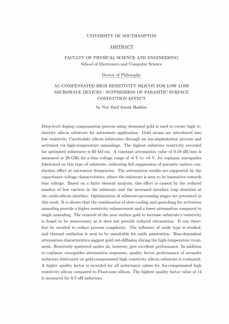
ABSTRACT
FACULTY OF PHYSICAL SCIENCE AND ENGINEERING
School of Electronics and Computer Science
Doctor of Philosophy
AU-COMPENSATED HIGH RESISTIVITY SILICON FOR LOW LOSS
MICROWAVE DEVICES - SUPPRESSION OF PARASITIC SURFACE
CONDUCTION EFFECT
by Nur Zatil Ismah Hashim
Deep-level doping compensation process using elemental gold is used to create high re-
sistivity silicon substrate for microwave application. Gold atoms are introduced into
low resistivity Czochralski silicon substrates through an ion-implantation process and
activated via high-temperature annealings. The highest substrate resistivity recorded
for optimised substrates is 60 kΩ-cm. A constant attenuation value of 0.19 dB/mm is
measured at 20 GHz for a bias voltage range of -6 V to +6 V, for coplanar waveguides
fabricated on this type of substrate, indicating full suppression of parasitic surface con-
duction effect at microwave frequencies. The attenuation results are supported by the
capacitance-voltage characteristics, where the substrate is seen to be insensitive towards
bias voltage. Based on a finite element analysis, this effect is caused by the reduced
number of free carriers in the substrate and the increased interface trap densities at
the oxide-silicon interface. Optimisation of substrate-processing stages are presented in
this work. It is shown that the combination of slow-cooling and quenching for activation
annealing provide a higher resistivity enhancement and a lower attenuation compared to
single annealing. The removal of the near surface gold to increase substrate’s resistivity
is found to be unnecessary as it does not provide reduced attenuation. It can there-
fore be avoided to reduce process complexity. The influence of oxide type is studied,
and thermal oxidation is seen to be unsuitable for oxide passivation. Bias-dependent
attenuation characteristics suggest gold out-diffusion during the high-temperature treat-
ment. Reactively sputtered oxides do, however, give excellent performance. In addition
to coplanar waveguides attenuation responses, quality factor performance of meander
inductors fabricated on gold-compensated high resistivity silicon substrate is evaluated.
A higher quality factor is recorded for all inductance values for Au-compensated high
resistivity silicon compared to Float-zone silicon. The highest quality factor value of 14
is measured for 0.7-nH inductors.


Declaration of Authorship
I, Nur Zatil Ismah Hashim , declare that the thesis entitled Au-compensated High Resis-
tivity Silicon for Low Loss Microwave Devices - Suppression of Parasitic Surface Con-
duction Effect and the work presented in the thesis are both my own, and have been
generated by me as the result of my own original research. I confirm that:
• this work was done wholly or mainly while in candidature for a research degree at
this University;
• where any part of this thesis has previously been submitted for a degree or any
other qualification at this University or any other institution, this has been clearly
stated;
• where I have consulted the published work of others, this is always clearly at-
tributed;
• where I have quoted from the work of others, the source is always given. With the
exception of such quotations, this thesis is entirely my own work;
• I have acknowledged all main sources of help;
• where the thesis is based on work done by myself jointly with others, I have made
clear exactly what was done by others and what I have contributed myself;
• parts of this work have been published as shown in the List of Publications;
Signed:.......................................................................................................................
Date:..........................................................................................................................
v
List of Publications
N.Z.I. Hashim, Abuelgasim A., De Groot C.H., (2013) Coplanar waveguides on
gold-doped high resistivity silicon for 67-GHz microwave application, RF and
Microwave Conference (RFM),2013 IEEE International, Penang, Malaysia.
Abuelgasim A., N.Z.I. Hashim, Chong, H.M.C., Ashburn, P., De Groot C.H., (2014)
Low loss 67-GHz coplanar waveguides and spiral inductors on 100 kΩcm
gold-doped high resistivity Cz-Silicon, Silicon Monolithic Integrated Circuits in
RF Systems (SiRF), 2014 IEEE 14th Topical Meeting on, Newport Beach, California,
USA.
N.Z.I. Hashim, Abuelgasim A., De Groot C.H., (2015) Low loss microwave sub-
strate using deep-level doping compensation, NANO Day Poster Session, Southamp-
ton, United Kingdom.
N.Z.I. Hashim, Abuelgasim A., De Groot C.H., (2014) Suppression of parasitic
surface conduction in Au-compensated high resistivity silicon for 40-GHz
RF-MMIC application, Microwave Conference (APMC), 2014 Asia-Pacific, Sendai,
Japan.
K. Mallik, A. Abuelgasim, N.Hashim, P.Ashburn, C.H. de Groot, (2014) Analytical
and numerical model of spiral inductors on high resistivity silicon substrates,
Solid-State Electronics, 93, 43-48.
N.Z.I. Hashim, Abuelgasim A., De Groot C.H., (2015) Suppression of parasitic
surface conduction in Au-compensated high resistivity silicon for microwave
application, ECS Industrial Advisory Board Poster Session, Southampton, United
Kingdom.
N.Z.I. Hashim, Abuelgasim A., De Groot C.H., (2015) Gold-compensated high re-
sistivity silicon as low loss microwave substrate, IEEE Transactions on Microwave
Theory and Techniques (To be submitted).
vi
Acknowledgements
”Life is a great big canvas, and you should throw all the paint you can on it.”
Quoted from Danny Kane, that was the first line that I wrote in my logbook when I
started my PhD. It was never about the qualification alone, it was always about the
journey, the experience, and most importantly, the people; the loved ones that I left
behind to come to Southampton, and the cherished ones that I met here, who have
made this chapter of my life nothing less than meaningful.
Surely not the least to thank for, Professor Kees de Groot, for the tremendous amount of
guidance in completing my PhD, for the supervision and the financial support that you
have given me, you are a star. Thank you for putting up with me and my incompetencies,
and I hope I have not been too much of a burden as your student. A special thanks
goes to Dr Ahmed Abuelgasim, Dr Yudong Wang and Dr Ruomeng Huang for their
time in helping me out with the fabrication work in the cleanroom, as well as the
device characterisation process in the measurement lab. To all the other inhabitants of
Southampton Nanofabrication Center, you have made it a less scarier jungle for me to
dig in, by providing sufficient needs and enough support throughout the entire years.
My heartiest appreciation goes to my parents, Hashim and Salihah, for the endless
support and encouragement, for the years spent worrying about their youngest daughter
who does not seem to want to find her way back home (Don’t worry, I’m coming home
soon!), for the prayers, for the love and care that they have shown me throughout these
years, for that, I thank you. And I love you. To my sister and my brother, Nur Awanis
and Ammar Nasran, no thanks to you for the naggings and the bullies! However, I really
could not thank you enough for taking care of Abah and Mama whilst I’m away, and for
having a bunch of wonderful children whom I miss dearly everyday; Amsyar, Assyifa,
Aafiyah, Iris and Ammar Jr. To these five teletubbies, Achu loves you so very much!
To the person whom I call a friend, the best one at it, you should know that my eyes
were well up with tears even before I mentioned your name here. Dear Azira, you have
always been there for me. To share the laughter and the tears, the secrets and the
confessions, the idiocy and the craziness that no one knows apart from you. For holding
me up when I’m feeling down, for gathering up my courage when I have none, for being
a wonderful friend when I’m being the reckless one, and for all of that, thank you for
sticking around.
The next dedication goes to 15 Honeysuckle Road, the house where I met my friends for
life. To my evil twin, Khaira, I miss you and I miss us. Even though the endings are
not as what we expected it to be, I hope you know that, deep down inside my heart,
you are a friend that I treasure so much. I wish you well and I wish you success and I
hope someday and somewhere we will find our way to one another again. To Asmah and
vii
viii
Lynn, the first six months of my stay in Southampton would not have been colourful
without you two.
My sources of sanity in the office and my lunch buddies, Katrina and Eleni, thank you
for all the shared gossips, the giggles and most importantly, the good company for the
past four years. The rest of the NANO girls, all of you have been amazing. Keep the girl
power alive! Not to forget the people in Bay 4 of NANO and Silicon Photonics Research
Groups, especially Stevan, Nikos, Taharh and Despina, thank you for the wisdom.
My deepest appreciation also goes to the people who have been in and out of my life, my
greatest source of good distraction and sometimes also served as my source of heartbreak.
Despite the countless hours I have spent on running to take my mind off you, each one
of you gave me one good lesson. I have now learnt to wait for the magic, and settle not
for the ordinary. After all, this is only another chapter of my life that I have painted.
Last but not least, this PhD would not have been possible without the full financial
support entitled to me by the Goverment of Malaysia and specifically my employers, the
Ministry of Higher Education and the University of Science, Malaysia. This debt will be
dutifully repaid with the years that I am going to serve you for once I settle for home.
With the remaining white spaces that I have on the canvas, I am thrilled to the more
exciting episode soon!
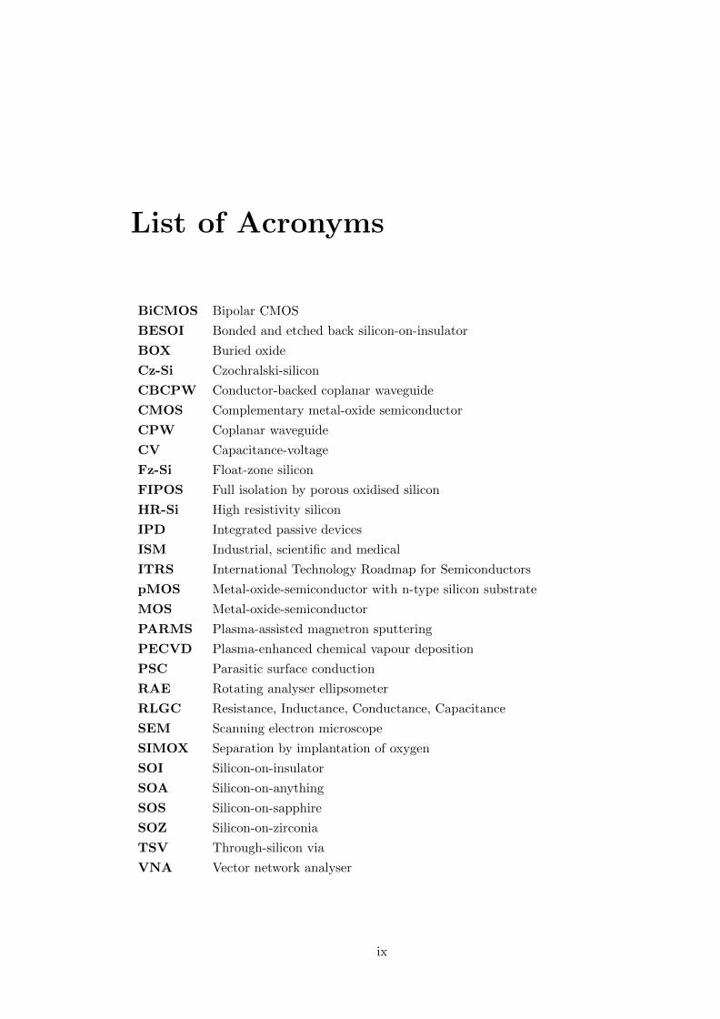
List of Acronyms
BiCMOS Bipolar CMOS
BESOI Bonded and etched back silicon-on-insulator
BOX Buried oxide
Cz-Si Czochralski-silicon
CBCPW Conductor-backed coplanar waveguide
CMOS Complementary metal-oxide semiconductor
CPW Coplanar waveguide
CV Capacitance-voltage
Fz-Si Float-zone silicon
FIPOS Full isolation by porous oxidised silicon
HR-Si High resistivity silicon
IPD Integrated passive devices
ISM Industrial, scientific and medical
ITRS International Technology Roadmap for Semiconductors
pMOS Metal-oxide-semiconductor with n-type silicon substrate
MOS Metal-oxide-semiconductor
PARMS Plasma-assisted magnetron sputtering
PECVD Plasma-enhanced chemical vapour deposition
PSC Parasitic surface conduction
RAE Rotating analyser ellipsometer
RLGC Resistance, Inductance, Conductance, Capacitance
SEM Scanning electron microscope
SIMOX Separation by implantation of oxygen
SOI Silicon-on-insulator
SOA Silicon-on-anything
SOS Silicon-on-sapphire
SOZ Silicon-on-zirconia
TSV Through-silicon via
VNA Vector network analyser
ix

Contents
Declaration of Authorship v
List of Publications vi
Acknowledgements vii
List of Acronyms ix
1 Introduction 1
1.1 High resistivity substrate for low-loss microwave application . . . . . . . . 1
1.2 Silicon as microwave substrate . . . . . . . . . . . . . . . . . . . . . . . . 3
1.3 Parasitic surface conduction effect in bulk high resistivity silicon substrate 5
1.4 Thesis outline . . . . . . . . . . . . . . . . . . . . . . . . . . . . . . . . . . 7
2 Realisation of Au-compensated High Resistivity Silicon 9
2.1 Impurities in Silicon . . . . . . . . . . . . . . . . . . . . . . . . . . . . . . 9
2.2 Deep Level Doping Compensation . . . . . . . . . . . . . . . . . . . . . . 12
2.3 Gold (Au) as Deep Level Dopant . . . . . . . . . . . . . . . . . . . . . . . 16
2.4 Implementation of Au-compensated HR-Si in microwave technology . . . 20
2.5 Developing Au-compensated High Resistivity Silicon Substrates . . . . . . 22
2.6 Summary . . . . . . . . . . . . . . . . . . . . . . . . . . . . . . . . . . . . 26
3 Design and Fabrication of Microwave Devices 27
3.1 Capacitor design . . . . . . . . . . . . . . . . . . . . . . . . . . . . . . . . 27
3.2 Coplanar waveguide design . . . . . . . . . . . . . . . . . . . . . . . . . . 28
3.3 Meander inductor design . . . . . . . . . . . . . . . . . . . . . . . . . . . . 34
3.4 Fabrication of devices on Au-compensated HR-Si substrates . . . . . . . . 41
3.5 Summary . . . . . . . . . . . . . . . . . . . . . . . . . . . . . . . . . . . . 51
4 Evaluation of Surface Charge Layers in MOS Capacitors on High Re-sistivity Silicon 53
4.1 Surface Conduction Effect Associated with Thermally Oxidised Silicon . . 53
4.2 Capacitance-Voltage Characterisation . . . . . . . . . . . . . . . . . . . . 62
4.3 C-V Simulation of MOS Capacitors on High Resistivity Substrates . . . . 66
4.4 Surface Charge Effects at Si-SiO2 Interface . . . . . . . . . . . . . . . . . 69
4.5 Summary . . . . . . . . . . . . . . . . . . . . . . . . . . . . . . . . . . . . 73
5 Suppression of Parasitic Surface Conduction using CPW Loss Analysis 75
5.1 Attenuation Loss Mechanism of a Coplanar Waveguide . . . . . . . . . . . 75
xi
xii CONTENTS
5.2 Characterisation of CPW Loss using Transmission Line Model . . . . . . 79
5.3 Attenuation Loss of CPW on Au-compensated HR-Si Substrates . . . . . 82
5.4 Suppression of Parasitic Surface Conduction (PSC) using Au-Si Substrates 85
5.5 Effective Resistivity of Au-compensated HR-Si . . . . . . . . . . . . . . . 89
5.6 Summary . . . . . . . . . . . . . . . . . . . . . . . . . . . . . . . . . . . . 93
6 Improving Quality Factor of Meander Inductors 95
6.1 Quality factor of a Meander Inductor . . . . . . . . . . . . . . . . . . . . . 96
6.2 S-parameter Measurement Setup & Results . . . . . . . . . . . . . . . . . 98
6.3 Quality factor of Meander Inductor on Au-Si substrate . . . . . . . . . . . 104
6.4 Summary . . . . . . . . . . . . . . . . . . . . . . . . . . . . . . . . . . . . 107
7 Summary & Outlook 109
7.1 Summary . . . . . . . . . . . . . . . . . . . . . . . . . . . . . . . . . . . . 109
7.2 Outlook . . . . . . . . . . . . . . . . . . . . . . . . . . . . . . . . . . . . . 112
References 115
Appendix A: Extraction of Effective Resistivity using CPW TransmissionLine 125
Appendix B: RLC Circuit Analysis using SONNET 133
Appendix C: Attenuation characteristics for CPWs 139
Chapter 1
Introduction
1.1 High resistivity substrate for low-loss microwave ap-
plication
The need for high-speed electronic devices and circuits has augmented the development
of monolithic microwave integrated circuits (MMICs), whereby the production of CMOS
and BiCMOS transistors have been made capable of operating at microwave frequencies
(ranging between 300 MHz - 300 GHz) [1]. The integration of microwave circuitry has
led to the incorporation of wireless communication in today’s cellular (or mobile) and
data communication network. Applications of these include (but are not limited to) the
operation of Wi-Fi and Bluetooth in the ISM band range [2] for unlicensed usage.
In order to operate in such a super high frequency (SHF) environment, MMIC devices
need to be fabricated on low loss, high resistivity substrates. This is achieved by having
a significantly reduced number of background free carriers in the substrate, which con-
tribute to substrate losses at high frequency operation. The use of high resistivity sub-
strates for microwave application has been proven to aid improvement on noise isolation
and to provide high power transmission efficiency. This will benefit passive components
and interconnectors for example, planar inductors, capacitors, coplanar waveguides and
microstrips [3–6].
The production of high resistivity substrates for MMIC applications has always been
associated with III-V semiconductor materials such as GaAs, GaN and InP, due to the
wide band-gap nature of the compound substrates. Having a wide energy band-gap en-
sures suppression of electrical current conduction which consequently leads to substrate
isolation from device operation [7]. Despite their semi-insulating properties, the com-
plexity in creating compound semiconductors (for example, lattice-mismatch problems)
increases fabrication cost. Perceiving this as an undesirable factor, silicon, came back
into the picture offering less complexity and lower fabrication and manufacturing costs.
1
2 Chapter 1 Introduction
However, creating very high resistivity bulk Si substrates is not straightforward since the
presence of background carriers generated during monocrystalline Si growth hindered its
potential development as a microwave substrate. This is because background carriers in
bulk Si create significant current conduction paths that contribute to substrate losses at
microwave range. To solve this issue, silicon-on-anything (SOA) and silicon-on-insulator
(SOI) technologies were introduced, where the former was realised by transferring silicon-
based, fully-processed ICs, onto material such as glass [8, 9].
The latter was firstly introduced with thin film Si being chemically vapour-deposited
on highly-insulated elements such as sapphire and zirconia to form silicon-on-sapphire
(SOS) [10] and silicon-on-zirconia (SOZ) [11]. Instead of depositing thin film Si on
top of other insulators, an alternative approach, known as FIPOS and SIMOX, can be
used in which a thin layer of Si film is separated from its bulk structure by oxidised
[12] or implanted SiO2 [13], respectively. Apart from the mentioned methods, more
commercially available SOI were introduced through wafer-bonding techniques called
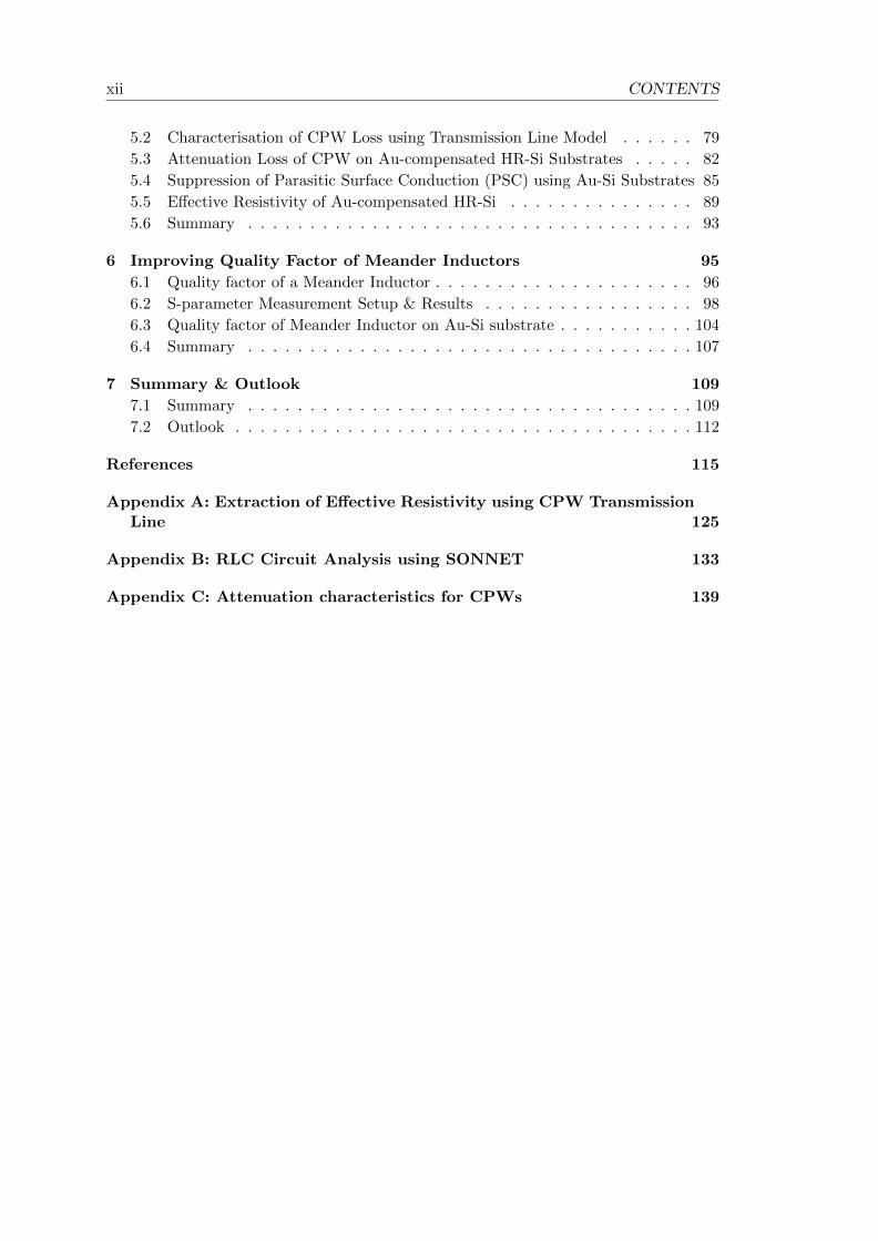
Bonded and Etched Back SOI (BESOI) [14] and Smart CutTM [15]. Two Si wafers,
including one which has been oxidised or implanted, were bonded together. The upper
top undergoes thinning process until the required thickness is achieved for BESOI, or
just above the implanted area for the case of Smart-CutTM.
Figure 1.1: Smart CutTM process engineered by Soitec Inc. for production ofSOI wafers [15]
Despite extensive research conducted on SOI technology to create silicon-based mi-
crowave substrates, self-heating issues and its associated thermal breakdown caused by
separation of devices from bulk Si structures have always been a pressing matter [16–20].
Having thinner SOI oxides to solve thermal isolation problems however will only reduce
substrate’s isolation from eddy currents. Hence, there continues to be a constant need
Chapter 1 Introduction 3
to develop high resistivity bulk Si substrate as an alternative to SOI wafers, thereby
eliminating the structural complexity.
1.2 Silicon as microwave substrate
International Technology Roadmap for Semiconductors (ITRS) has underlined the im-
portance of high resistivity silicon substrates for integration of passive components in
mixed analog/digital RF CMOS devices [21]. Although the emphasis is on compound Si
and SOI technology, research on high resistivity bulk Si substrate is becoming increas-
ingly important given its reduced structure complexity, which is translated into reduced
fabrication cost.
The basic principle of creating high resistivity bulk Si substrates is to reduce the con-
centration of background free carriers that provide alternative current conduction paths
inside the substrate and consequently generate losses at microwave frequencies. The
presence of these parasitic carriers originates from inevitable contamination that occurs
during monocrystalline Si growth in the Czochralski process (Cz-Si).
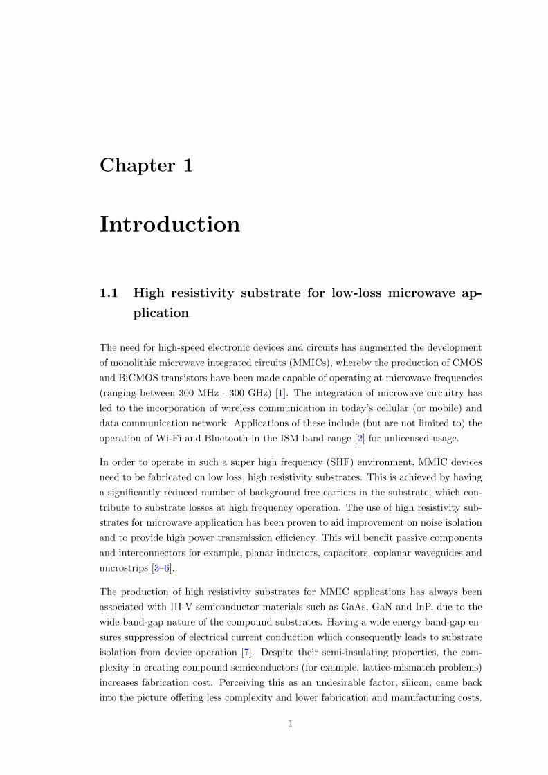
Figure 1.2 illustrates Czochralski crystal-pulling process used to produce monocrystalline
Si ingots. High purity polycrystalline Si, called electronic grade silicon are filled into a
silica (or quartz) crucible and melted over a high temperature before being pulled out
through a crystal-orientated seed to create Si ingot of a specific pulling rate-dependent
diameter.
Figure 1.2: Czochralski silicon process [22]
One source of contaminations comes from the silica crucible that holds the melt. During
high temperature treatment, the crucible is slightly dissolved and releases 5 to 20 of parts
4 Chapter 1 Introduction
per million atoms (ppma) oxygen which will then be transported around the vessel in
the form of silicon monoxide. In addition to oxygen, a reaction between the crucible and
the graphite susceptor (located underneath the crucible to provide mechanical strength)
produces carbon monoxide. Apart from oxygen and carbon, low-level contamination
also comes from impurities such as boron and phosphorus due to the incorporation of
these elements used to generate doped Si substrates for electrical modulation.
The quickest solution to address this issue would be to use the Float-zone (Fz-Si) method
for growing Si, where the absence of a silica crucible reduces the level of contamination
in the growth process. Nowadays, Float-zone silicon wafers with bulk resistivities up to
70 kΩ-cm, called HiResTM, are commercially available for the use of microwave circuits
and devices in GHz and THz range [23]. However, the largest wafer diameter produced
so far using this method is 8”. From manufacturing point of view, this means an increase
in production cost since, the current standard wafer size for modern CMOS processing
is 12” [24]. For a large-scaled, low-cost production, the only alternative to Fz-Si still
is Cz-Si. Since growth contamination in Cz-Si is unavoidable, research has been done
in terms of modification of its crystalline structure to reduce mobile background free
carriers in Cz-Si substrates, and therefore increasing the substrate’s bulk resistivity.
One way to achieve this is by employing the proton implantation method. The basic
principle of this method is bombardment of protons through the Si surface into its bulk
structure, creating defects that trap mobile carriers, stopping them from conducting
freely inside the structure. In 1978, Aoki et al. proposed the growth of high resistivity
silicon through an oxygen or nitrogen ion beam implantation technique [25]. Using an
implantation energy of 200 keV, oxygen was injected through polycrystalline silicon,
amorphous silicon and a single crystal layer, to produce semi-insulating Si layer, with
resistivities between 107 to 1011 Ω-cm.
The work was followed by Li et al. in 1989 where they managed to produce a silicon
layer with a resistivity of 103 Ω-cm, through proton-implantation at an energy of 180
keV, followed by two-step annealing process [26]. The formation of a buried defect layer
and impurity-gettering create a defect-free zone at the top of the silicon layer. In 1998,
Liao made use of a higher implantation energy (30 MeV) to accelerate protons and
create deep level traps in a lightly-doped silicon wafer, increasing its resistivity to 106
Ω-cm [27]. Using a slightly lower implantation energy than Liao i.e. 10 MeV, and adding
a two-step annealing process in his work, Wu et al. [28] succeeded in producing silicon
wafer of the same resistivity. Rashid et al. reported a resistivity value of 105 Ω-cm,
achieved through their six-step implantation method using an implantation energy of
17.4 MeV [29].
Successful attempts in creating high resistivity bulk Cz-Si has led to its potential as a
microwave substrate, comparable to commercially available semi-insulating III-Vs and
SOIs. However, focussing on increasing bulk resistivity is not the only issue that matters
Chapter 1 Introduction 5
in developing low loss microwave substrate. The existence of parasitic surface conduc-
tion (PSC) at bulk Si surface causes degradation of overall substrate’s resistivity and
introduces additional losses for devices operating at high frequency.
1.3 Parasitic surface conduction effect in bulk high resis-
tivity silicon substrate
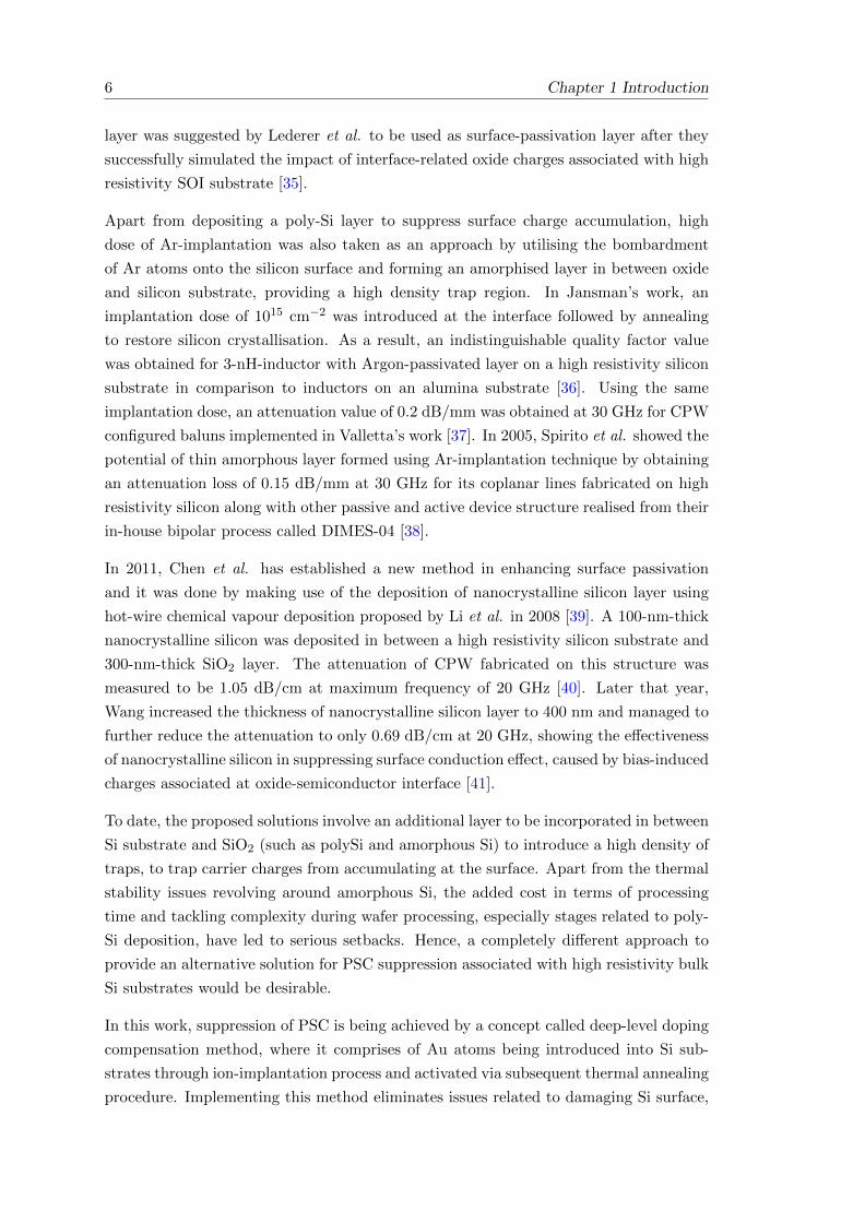
Parasitic surface conduction (PSC) effect was first explained by Reyes et al. where an
increase in coplanar waveguide (CPW) attenuation was reported in both work for CPWs
fabricated on high resistivity Si substrates [30, 31]. According to Reyes, there exists a
formation of either accumulation or inversion at the Si surface which can potentially
cause a drop in surface resistivity and eventually contribute to an increase in losses. In
1999, Wu et al. presented quantitative analysis for Reyes’ hypothesis, confirming the
existence of a low resistivity region at oxide-semiconductor surface, due to population
of carriers during accumulation or inversion [32].
Figure 1.3: Non-continuous oxide pattern between HR-Si substrate and CPWconductor line [32].
He also proposed the use of a non-continuous oxide pattern to reduce attenuation loss
since losses due to the inversion layer, situated right beneath the CPW lines, were said
to be insignificant. It was said that the loss was mainly contributed to the continuous
oxide pattern. In addition to that, non-continuous patterns allow DC-blocking role to
be taken by the readily formed thin layer native silicon oxide when exposed to air at
room temperature. The proposed structure is shown in Figure 1.3, where the loss was
recorded to decrease from 18 to 3 dB/cm at 30 GHz.
However, this has not been seen as an ideal, reliable and repetitive solution. Later the
same year, Gamble et al. came up with the idea of introducing a high density of traps in
between the oxide-silicon interface in order to trap electrons and prevent low resistivity
areas, whilst still having a continuous oxide to act as the passivation layer [33]. A 0.6-µm-
thick polycrystalline silicon was used as the trapping layer to give an attenuation loss of
1.08 dB/cm at 30 GHz, a value lower than the one obtained by Wu. Following Gamble’s
work, more work has been conducted on introducing trap-rich layers to surface-passivate
high resistivity silicon. Lue incorporated a 300-nm-thick polysilicon film beneath a 100-
nm-thick SiO2 layer, obtaining low insertion loss [34]. The same thickness of polysilicon
6 Chapter 1 Introduction
layer was suggested by Lederer et al. to be used as surface-passivation layer after they
successfully simulated the impact of interface-related oxide charges associated with high
resistivity SOI substrate [35].
Apart from depositing a poly-Si layer to suppress surface charge accumulation, high
dose of Ar-implantation was also taken as an approach by utilising the bombardment
of Ar atoms onto the silicon surface and forming an amorphised layer in between oxide
and silicon substrate, providing a high density trap region. In Jansman’s work, an
implantation dose of 1015 cm−2 was introduced at the interface followed by annealing
to restore silicon crystallisation. As a result, an indistinguishable quality factor value
was obtained for 3-nH-inductor with Argon-passivated layer on a high resistivity silicon
substrate in comparison to inductors on an alumina substrate [36]. Using the same
implantation dose, an attenuation value of 0.2 dB/mm was obtained at 30 GHz for CPW
configured baluns implemented in Valletta’s work [37]. In 2005, Spirito et al. showed the
potential of thin amorphous layer formed using Ar-implantation technique by obtaining
an attenuation loss of 0.15 dB/mm at 30 GHz for its coplanar lines fabricated on high
resistivity silicon along with other passive and active device structure realised from their
in-house bipolar process called DIMES-04 [38].
In 2011, Chen et al. has established a new method in enhancing surface passivation
and it was done by making use of the deposition of nanocrystalline silicon layer using
hot-wire chemical vapour deposition proposed by Li et al. in 2008 [39]. A 100-nm-thick
nanocrystalline silicon was deposited in between a high resistivity silicon substrate and
300-nm-thick SiO2 layer. The attenuation of CPW fabricated on this structure was
measured to be 1.05 dB/cm at maximum frequency of 20 GHz [40]. Later that year,
Wang increased the thickness of nanocrystalline silicon layer to 400 nm and managed to
further reduce the attenuation to only 0.69 dB/cm at 20 GHz, showing the effectiveness
of nanocrystalline silicon in suppressing surface conduction effect, caused by bias-induced
charges associated at oxide-semiconductor interface [41].
To date, the proposed solutions involve an additional layer to be incorporated in between
Si substrate and SiO2 (such as polySi and amorphous Si) to introduce a high density of
traps, to trap carrier charges from accumulating at the surface. Apart from the thermal
stability issues revolving around amorphous Si, the added cost in terms of processing
time and tackling complexity during wafer processing, especially stages related to poly-
Si deposition, have led to serious setbacks. Hence, a completely different approach to
provide an alternative solution for PSC suppression associated with high resistivity bulk
Si substrates would be desirable.
In this work, suppression of PSC is being achieved by a concept called deep-level doping
compensation method, where it comprises of Au atoms being introduced into Si sub-
strates through ion-implantation process and activated via subsequent thermal annealing
procedure. Implementing this method eliminates issues related to damaging Si surface,
Chapter 1 Introduction 7
through bombardment of atoms that occur during the Si-amorphisation process.It also
avoids the underlying physical and chemical complexities seen when using additional
poly-Si or nanocrystalline Si layers on top of high resistivity Si substrates.
Using low-cost Czochralski-processed Si substrates as the starting material, deep-level
doping compensation approach is seen as a promising candidate to create high resistivity
Si wafers with full suppression of PSC effect, with a less-complex process procedures
contributing to reduced fabrication costs.
1.4 Thesis outline
The potential of deep level doping compensation method to suppress parasitic surface
conduction effect on high resistivity bulk silicon substrates for microwave application
is being studied in this work. Electrical and microwave components were designed,
software-simulated and fabricated onto Au-compensated high resistivity bulk Si sub-
strates (HR-Si) to observe its potential as low-loss microwave substrate by providing a
more conducive platform for reduction of background free carriers and suppression of
PSC-dependent charge carriers inside Si substrates.
Chapter 2 explains the underlying theory and potential microwave applications of high
resistivity Si substrates developed through deep-level doping compensation method. An
in-depth analysis on the creation of Au-compensated HR-Si substrates is discussed in
the later section, which include the introduction of Au atoms into Si through ion im-
plantation and its subsequent activation annealing procedures.
Chapter 3 discusses the electrical and microwave components used in this work with the
basic metal-oxide-silicon structure; capacitors, coplanar waveguides and meander induc-
tors. The chosen design for each components is explained and examined before being
carefully realised onto Au-compensated HR-Si substrates through a series of fabrication
processes. Capacitor structure was used to characterise the behaviour of bias-dependent
charge carriers associated with Si-SiO2 interface whereas coplanar waveguides and me-
ander inductors were used to study the microwave loss properties of Au-compensated Si
substrates with relation to PSC effect at the Si surface.
Chapter 4 evaluates the effect of surface charges from capacitance-voltage characterisa-
tion measured on the fabricated capacitor structures. Formation of charges at Si-SiO2 in-
terface provides an insight regarding the bahaviour of charge carriers in Au-compensated
HR-Si substrates with application of DC bias.
Chapter 5 examines the potential suppression of PSC effect using Au-compensated HR-Si
substrates, where coplanar waveguides were used as the analysed structure. Microwave
loss properties of this particular structure are discussed with respect to DC bias influence.
8 Chapter 1 Introduction
Characterisation of effective substrate resistivity is included at the end of the section to
quantify the effect of PSC on Au-compensated HR-Si.
Potential application of Au-compensated HR-Si substrates as microwave substrate is
further illustrated in Chapter 6. Microwave characteristics in terms of Q factor perfor-
mance of meander inductors are being analysed in this chapter with the effect of PSC
suppression on performance of integrated passive components is evaluated.
Last but not least, Chapter 7 represents the summary of work presented in the thesis.
Chapter 2
Realisation of Au-compensated
High Resistivity Silicon
Deep-level doping compensation method is used in this work to develop high resistivity
Si substrates for microwave application. Elemental gold (Au) is used to compensate
for background free carriers in low resistivity Czochralski silicon substrates, by creating
deep level traps inside Si band gap and enhancing substrate’s resistivity. Using this
method, Au is introduced into Si via ion-implantation process and activated through
high-temperature annealing procedure to achieve optimum level of compensation.
2.1 Impurities in Silicon
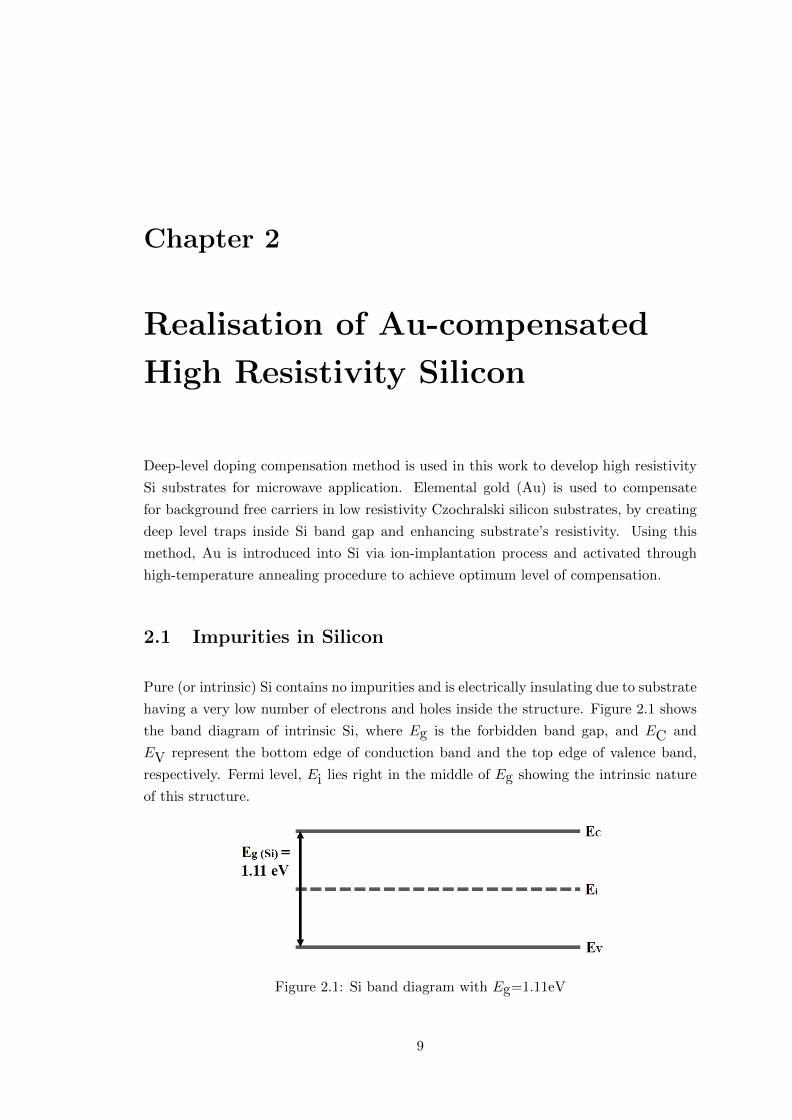
Pure (or intrinsic) Si contains no impurities and is electrically insulating due to substrate
having a very low number of electrons and holes inside the structure. Figure 2.1 shows
the band diagram of intrinsic Si, where Eg is the forbidden band gap, and EC and
EV represent the bottom edge of conduction band and the top edge of valence band,
respectively. Fermi level, Ei lies right in the middle of Eg showing the intrinsic nature
of this structure.
Figure 2.1: Si band diagram with Eg=1.11eV
9
10 Chapter 2 Realisation of Au-compensated High Resistivity Silicon
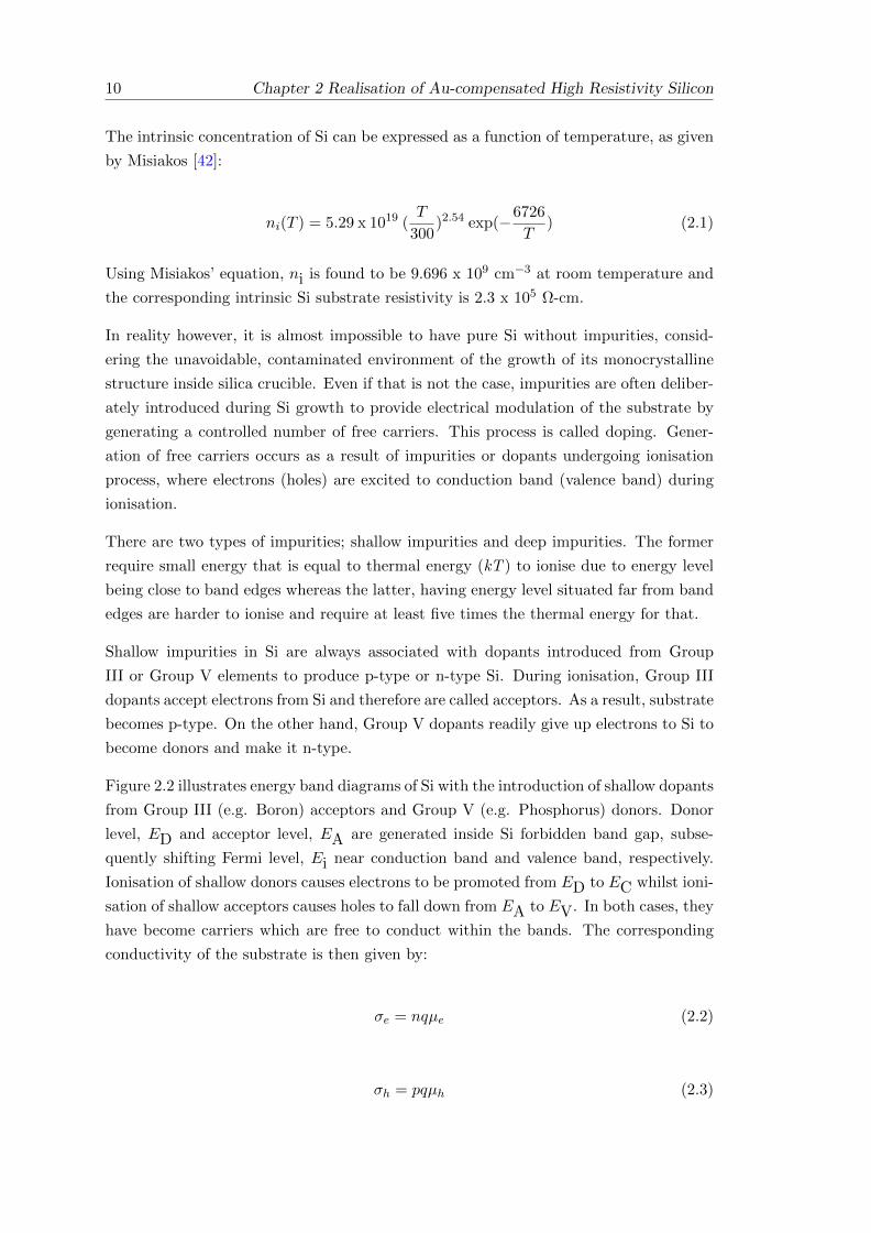
The intrinsic concentration of Si can be expressed as a function of temperature, as given
by Misiakos [42]:
ni(T ) = 5.29 x 10¹⁹ (T
300)2.54 exp(−6726
T) (2.1)
Using Misiakos’ equation, ni is found to be 9.696 x 109 cm−3 at room temperature and
the corresponding intrinsic Si substrate resistivity is 2.3 x 10⁵ Ω-cm.
In reality however, it is almost impossible to have pure Si without impurities, consid-
ering the unavoidable, contaminated environment of the growth of its monocrystalline
structure inside silica crucible. Even if that is not the case, impurities are often deliber-
ately introduced during Si growth to provide electrical modulation of the substrate by
generating a controlled number of free carriers. This process is called doping. Gener-
ation of free carriers occurs as a result of impurities or dopants undergoing ionisation
process, where electrons (holes) are excited to conduction band (valence band) during
ionisation.
There are two types of impurities; shallow impurities and deep impurities. The former
require small energy that is equal to thermal energy (kT ) to ionise due to energy level
being close to band edges whereas the latter, having energy level situated far from band
edges are harder to ionise and require at least five times the thermal energy for that.
Shallow impurities in Si are always associated with dopants introduced from Group
III or Group V elements to produce p-type or n-type Si. During ionisation, Group III
dopants accept electrons from Si and therefore are called acceptors. As a result, substrate
becomes p-type. On the other hand, Group V dopants readily give up electrons to Si to
become donors and make it n-type.
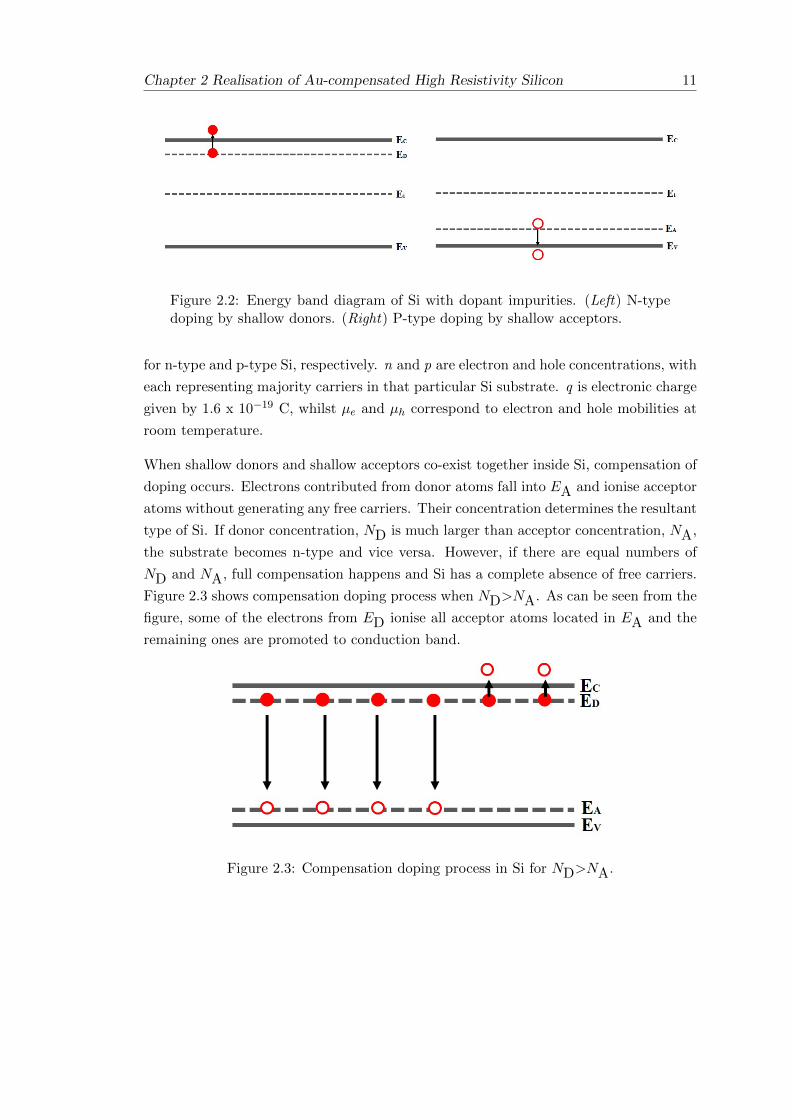
Figure 2.2 illustrates energy band diagrams of Si with the introduction of shallow dopants
from Group III (e.g. Boron) acceptors and Group V (e.g. Phosphorus) donors. Donor
level, ED and acceptor level, EA are generated inside Si forbidden band gap, subse-
quently shifting Fermi level, Ei near conduction band and valence band, respectively.
Ionisation of shallow donors causes electrons to be promoted from ED to EC whilst ioni-
sation of shallow acceptors causes holes to fall down from EA to EV. In both cases, they
have become carriers which are free to conduct within the bands. The corresponding
conductivity of the substrate is then given by:
σe = nqµe (2.2)
σh = pqµh (2.3)
Chapter 2 Realisation of Au-compensated High Resistivity Silicon 11
Figure 2.2: Energy band diagram of Si with dopant impurities. (Left) N-typedoping by shallow donors. (Right) P-type doping by shallow acceptors.
for n-type and p-type Si, respectively. n and p are electron and hole concentrations, with
each representing majority carriers in that particular Si substrate. q is electronic charge
given by 1.6 x 10⁻¹⁹ C, whilst µe and µh correspond to electron and hole mobilities at
room temperature.
When shallow donors and shallow acceptors co-exist together inside Si, compensation of
doping occurs. Electrons contributed from donor atoms fall into EA and ionise acceptor
atoms without generating any free carriers. Their concentration determines the resultant
type of Si. If donor concentration, ND is much larger than acceptor concentration, NA,
the substrate becomes n-type and vice versa. However, if there are equal numbers of
ND and NA, full compensation happens and Si has a complete absence of free carriers.
Figure 2.3 shows compensation doping process when ND>NA. As can be seen from the
figure, some of the electrons from ED ionise all acceptor atoms located in EA and the
remaining ones are promoted to conduction band.
Figure 2.3: Compensation doping process in Si for ND>NA.
12 Chapter 2 Realisation of Au-compensated High Resistivity Silicon
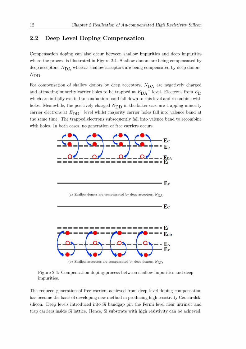
2.2 Deep Level Doping Compensation
Compensation doping can also occur between shallow impurities and deep impurities
where the process is illustrated in Figure 2.4. Shallow donors are being compensated by
deep acceptors, NDA whereas shallow acceptors are being compensated by deep donors,
NDD.
For compensation of shallow donors by deep acceptors, NDA are negatively charged
and attracting minority carrier holes to be trapped at EDA− level. Electrons from ED
which are initially excited to conduction band fall down to this level and recombine with
holes. Meanwhile, the positively charged NDD in the latter case are trapping minority
carrier electrons at EDD+ level whilst majority carrier holes fall into valence band at
the same time. The trapped electrons subsequently fall into valence band to recombine
with holes. In both cases, no generation of free carriers occurs.
(a) Shallow donors are compensated by deep acceptors, NDA
(b) Shallow acceptors are compensated by deep donors, NDD
Figure 2.4: Compensation doping process between shallow impurities and deepimpurities.
The reduced generation of free carriers achieved from deep level doping compensation
has become the basis of developing new method in producing high resistivity Czochralski
silicon. Deep levels introduced into Si bandgap pin the Fermi level near intrinsic and
trap carriers inside Si lattice. Hence, Si substrate with high resistivity can be achieved.
Chapter 2 Realisation of Au-compensated High Resistivity Silicon 13
Study shows that transition elements are potential candidates for this method [43]. The
key points in realising deep level doping compensation using transition metal elements
are the amount of energy required to induce ionisation i.e. deep level position, and
suitable dopant concentration to produce optimum compensation [44]. The first step
is to determine the Fermi level and this can be done by solving the charge neutrality
equation given by:
p+∑i
N+Di− n−
∑j
N−Aj = 0 (2.4)
where N+Di
and N−Aj is the ith ionised donor and j th ionised acceptor concentration for
a total impurity density of NDi and NAj respectively. For the purpose of this work, it is
assumed that only a pair of donor and acceptor levels are created by deep level dopants
in Si bandgap. Hence, the terms can be dropped to N+D and N−A , where the expressions
are derived as [45]:
N+D =
ND
1 + gDeEF−ED/kT + e2EF−EA−ED/kT(2.5)
N−A =NA
1 + gAeEA−EF /kT + eEA+ED−2EF /kT(2.6)
As for free hole and electron concentrations, n and p, the expressions are given by:
n = NCe−(EC−EF )/kT (2.7)
p = NV e−(EF−EV )/kT (2.8)
where k is the Boltzmann constant and T is the temperature taken as 300 K (room
temperature). NC and NV are effective density of states in the conduction band and
valence band respectively. In the case of silicon, these values are taken as 2.8 x 10¹⁹
cm−3 for NC and 1.04 x 1019 cm−3 for NV at room temperature [46]. Conduction band
energy level, EC equals energy band gap of silicon, which is 1.12 eV, with respect to
EV = 0 eV.
Equations above have been used together to solve for Equation 2.4 to find p and n. Once
these values have been found, resistivity, ρ can be calculated using:
ρ =1
σ=
1
nqµe + pqµh(2.9)
14 Chapter 2 Realisation of Au-compensated High Resistivity Silicon
where µe and µh are electron and hole mobility respectively. To analyse the impact of
incorporating deep level impurity to compensate for shallow levels in Si, calculations
have been done for p-type Si, Boron-doped with minimum concentration of 1013 cm−3
at T = 300 K. Acceptor energy level of Boron in Si was taken to be EV + 0.045 eV and
gD and gA are 2 and 4 respectively.
There were two variables that have been considered in this study:
1. Deep donor energy level below EC
2. Concentration of deep donor impurities in Si
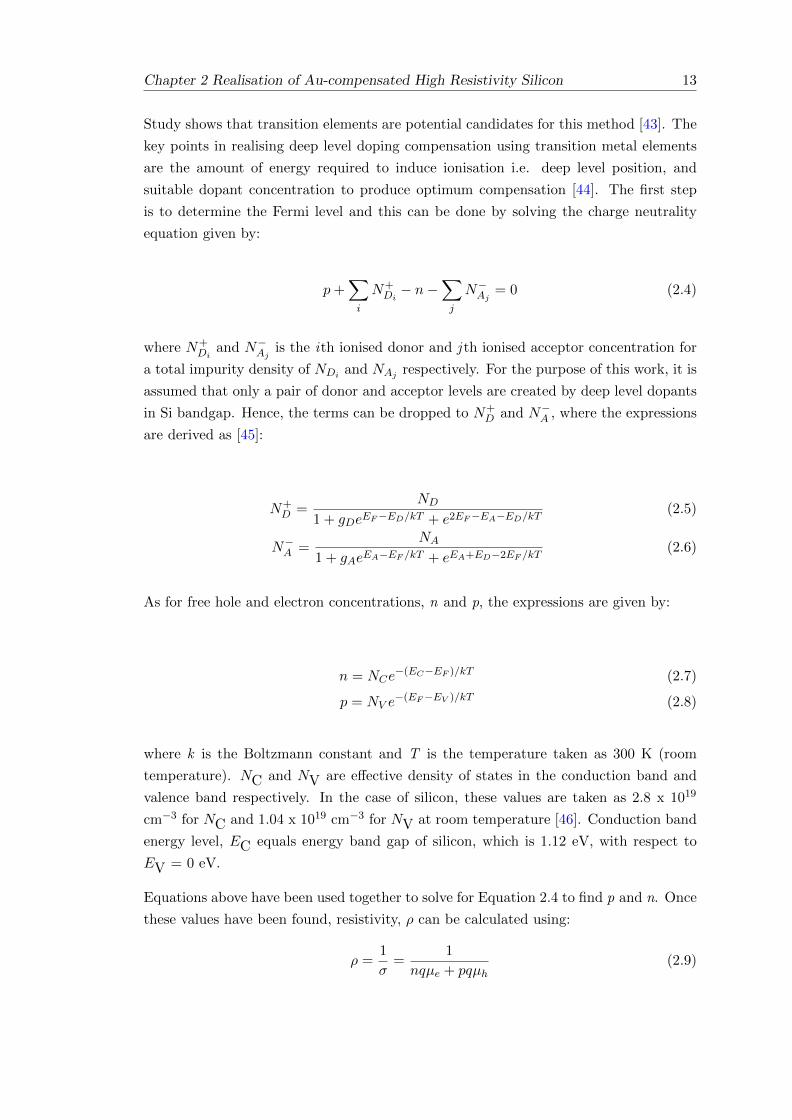
Figure 2.5 shows the corresponding Si resistivity at 300 K with respect to the concentra-
tion of donor impurity, with generic energy level positions below conduction band edge,
ED.
Figure 2.5: Calculated resistivity as a function of donor impurity concentrationsfor background B concentration of 1014 cm−3 at generic ED [44].
From the figure, it can be seen that the resistivity increases with increasing donor concen-
tration until it reaches a maximum value, and then falls back. Initially, ND is insufficient
to compensate for background Boron acceptors hence, resistivity is still low due to un-
dercompensation. Optimum compensation occurs when resistivity reaches its maximum
value, indicating that the number of donors exist exactly compensate for shallow Boron
acceptors whilst overcompensation due to excess number of ionised donors happens when
resistivity starts to decline with higher concentration of deep donor, making it prone to
becoming n-type.
Chapter 2 Realisation of Au-compensated High Resistivity Silicon 15
Element and site Donor level below NC Acceptor level above NVCo 0.89 0.82Pd 0.84 0.90Au 0.78 0.56Ag 0.75 0.55
Table 2.1: Substitutional position of energy levels of transition elements inSi [43].
Shallow donors can be distinguished from the figure (ED<0.3), in which the maxi-
mum resistivity has a sharp peak and the value occurs when donor concentration equals
background Boron concentration, ND = NA. The reason is that, donor energy level
is nearer to conduction band than intrinsic Fermi level, hence, almost all donors get
ionised and take part in compensating for shallow acceptors. A slight increase in con-
centration after this will cause overcompensation and change the material to n-type.
However, for ED≈0.5, energy level is closer to intrinsic Fermi level compared to conduc-
tion band. Less fraction of ionised donor indicates gradual change in compensation and
therefore, resistivity remains high over a wider range of donor concentration, provided
that ND>NA.
Therefore, using sufficiently deep donors, i.e. where ED≈0.5, a value of 5 x 10⁵ Ω-cm
can be achieved for p-type Si without the need of tight control over donor concentration
as the resistivity will remain high over a range of relatively low concentration values.
According to Mallik et al, the same conclusion can be drawn in the case of n-type Si,
where a sufficiently deep acceptor can be used to achieve high resistivity n-Si without
the need of tight control over its concentration.
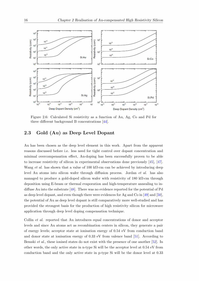
This study has been extended by including a number of transition elements, having
relatively deep donor and acceptor levels in Si. Table 2.1 shows the substitutional
position of energy levels of the elements. Using the equations gathered earlier in this
section, a graph of Si resistivity at 300 K is drawn as a function of Au, Ag, Co and
Pd for three different background Boron concentrations; 1013, 1014 and 1015 cm−3. The
results are shown in Figure 2.6.
As can be seen in the figure, the addition of deep dopant Au, Ag, Co and Pd into Si
increases the resistivity of silicon with at least three orders of magnitude. In general,
resistivity starts to increase at a value of ND = NA and remains high over a range
of concentrations, confirming the initial trend observed in Figure 2.5. Hence, these
elements are suitable for deep level doping compensation technique to compensate for
shallow acceptor/donor levels in silicon and increase its resistivity, with particularly the
Au and Ag acceptor levels near midgap being very suitable.
16 Chapter 2 Realisation of Au-compensated High Resistivity Silicon
Figure 2.6: Calculated Si resistivity as a function of Au, Ag, Co and Pd forthree different background B concentrations [44].
2.3 Gold (Au) as Deep Level Dopant
Au has been chosen as the deep level element in this work. Apart from the apparent
reasons discussed before i.e. less need for tight control over dopant concentration and
minimal overcompensation effect, Au-doping has been successfully proven to be able
to increase resistivity of silicon in experimental observations done previously [45], [47].
Wang et al. has shown that a value of 100 kΩ-cm can be achieved by introducing deep
level Au atoms into silicon wafer through diffusion process. Jordan et al. has also
managed to produce a gold-doped silicon wafer with resistivity of 180 kΩ-cm through
deposition using E-beam or thermal evaporation and high-temperature annealing to in-
diffuse Au into the substrate [48]. There was no evidence reported for the potential of Pd
as deep level dopant, and even though there were evidences for Ag and Co in [49] and [50],
the potential of Au as deep level dopant is still comparatively more well-studied and has
provided the strongest basis for the production of high resistivity silicon for microwave
application through deep level doping compensation technique.
Collin et al. reported that Au introduces equal concentrations of donor and acceptor
levels and since Au atoms act as recombination centers in silicon, they generate a pair
of energy levels; acceptor state at ionisation energy of 0.54 eV from conduction band
and donor state at ionisation energy of 0.33 eV from valence band [51]. According to
Bemski et al., these ionised states do not exist with the presence of one another [52]. In
other words, the only active state in n-type Si will be the acceptor level at 0.54 eV from
conduction band and the only active state in p-type Si will be the donor level at 0.33
Chapter 2 Realisation of Au-compensated High Resistivity Silicon 17
eV from valence band. Therefore, unlike Manganese which only creates deep level donor
in Si and can only compensate for p-type Si [53], Au can compensate for both n- and
p-type Si due to its deep level nature in both conditions. Not only that it can enhance
silicon resistivity, a large range of concentration can be used to achieve this, making it
desirably beneficial during wafer-processing stage.
Au can occupy both, interstitial and substitutional sites in silicon [54] but deep levels
in silicon are created only by Au occupying substitutional sites. Hence the diffusion
process needs to be well controlled to achieve the required substitutional positions.
Since substitutional Au has lower diffusivity than interstitial Au [55–57], diffusion of
Au occurs, first, predominantly in the interstitial sites before exchange of sites takes
place, and the occupancy becomes subsitutional. At temperature above 800 C, the
interchange between interstitial Au and substitutional Au is controlled by the ’kick-out’
mechanism [58]. This means that Au diffuses through lattice interstitial, kicks out a
silicon atom and substitute for its lattice position, where it is relatively immobile. The
mechanism can be shown as:
Aui ⇔ Aus + I (2.10)
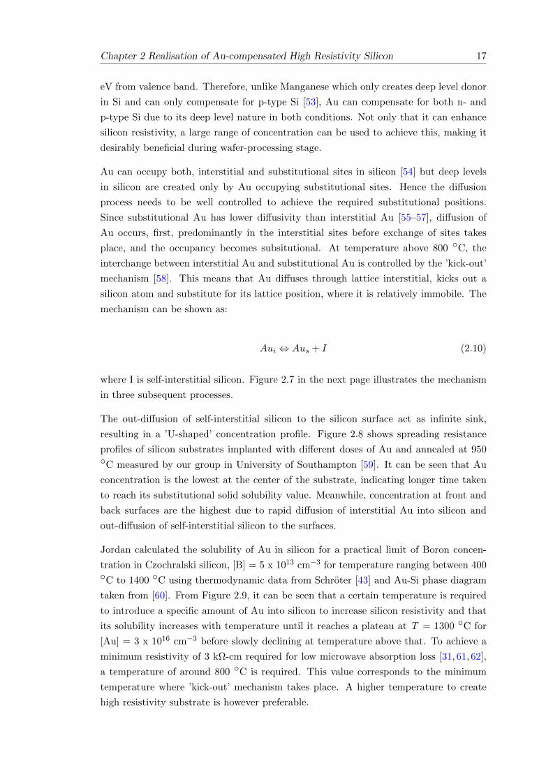
where I is self-interstitial silicon. Figure 2.7 in the next page illustrates the mechanism
in three subsequent processes.
The out-diffusion of self-interstitial silicon to the silicon surface act as infinite sink,
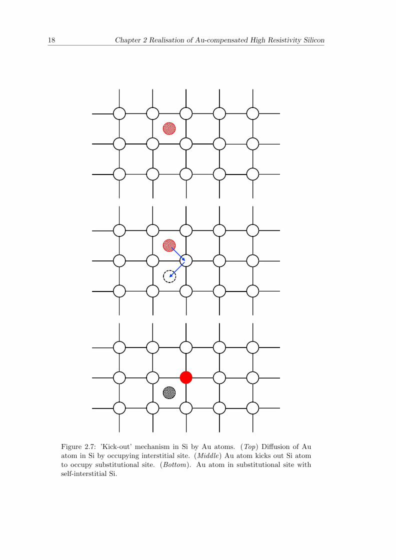
resulting in a ’U-shaped’ concentration profile. Figure 2.8 shows spreading resistance
profiles of silicon substrates implanted with different doses of Au and annealed at 950C measured by our group in University of Southampton [59]. It can be seen that Au
concentration is the lowest at the center of the substrate, indicating longer time taken
to reach its substitutional solid solubility value. Meanwhile, concentration at front and
back surfaces are the highest due to rapid diffusion of interstitial Au into silicon and
out-diffusion of self-interstitial silicon to the surfaces.
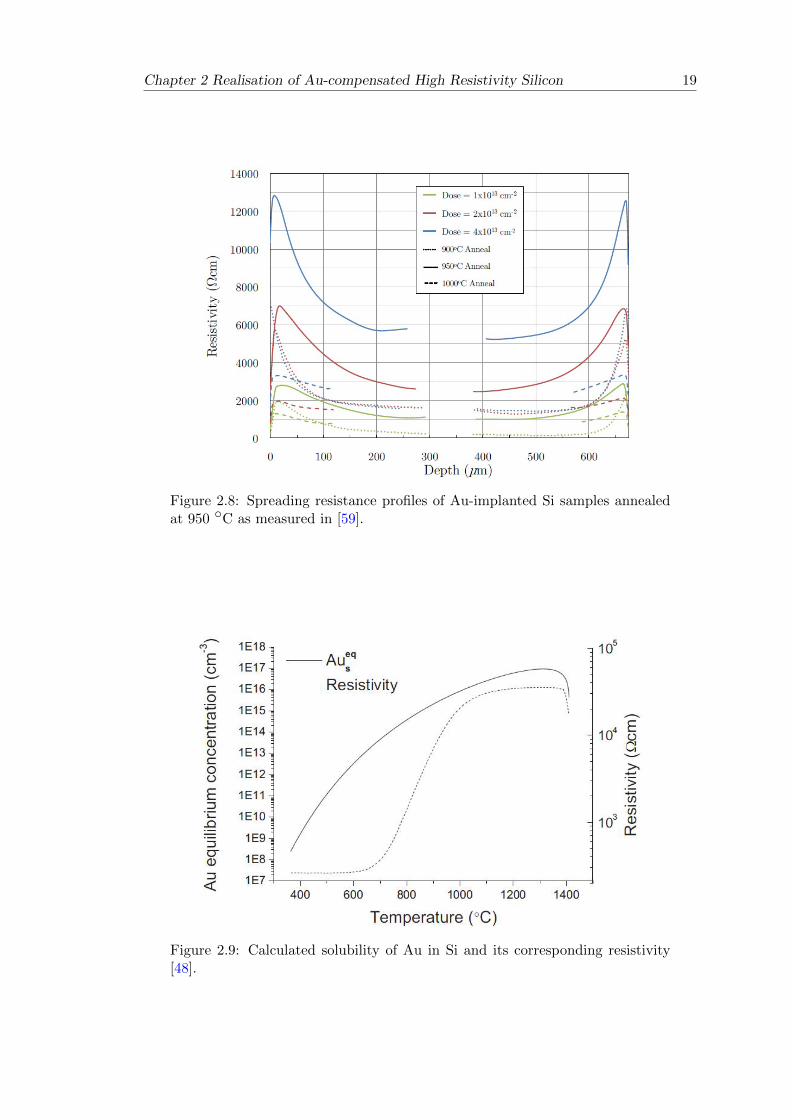
Jordan calculated the solubility of Au in silicon for a practical limit of Boron concen-
tration in Czochralski silicon, [B] = 5 x 1013 cm−3 for temperature ranging between 400C to 1400 C using thermodynamic data from Schroter [43] and Au-Si phase diagram
taken from [60]. From Figure 2.9, it can be seen that a certain temperature is required
to introduce a specific amount of Au into silicon to increase silicon resistivity and that
its solubility increases with temperature until it reaches a plateau at T = 1300 C for
[Au] = 3 x 1016 cm−3 before slowly declining at temperature above that. To achieve a
minimum resistivity of 3 kΩ-cm required for low microwave absorption loss [31, 61, 62],
a temperature of around 800 C is required. This value corresponds to the minimum
temperature where ’kick-out’ mechanism takes place. A higher temperature to create
high resistivity substrate is however preferable.
18 Chapter 2 Realisation of Au-compensated High Resistivity Silicon
Figure 2.7: ’Kick-out’ mechanism in Si by Au atoms. (Top) Diffusion of Auatom in Si by occupying interstitial site. (Middle) Au atom kicks out Si atomto occupy substitutional site. (Bottom). Au atom in substitutional site withself-interstitial Si.
Chapter 2 Realisation of Au-compensated High Resistivity Silicon 19
Figure 2.8: Spreading resistance profiles of Au-implanted Si samples annealedat 950 C as measured in [59].
Figure 2.9: Calculated solubility of Au in Si and its corresponding resistivity[48].
20 Chapter 2 Realisation of Au-compensated High Resistivity Silicon
2.4 Implementation of Au-compensated HR-Si in microwave
technology
High solubility implies high diffusivity [63]. The high diffusivity nature of Au serves as an
excellent metallisation contact material but is detrimental for silicon wafer-processing, as
Au may diffuse into the active region on silicon substrate, degrading device performance
through unwanted compensation or trappings. In response to this, the applications of
Au-compensated HR-Si substrates are only focussing on specific RF-MMIC technology
such as integrated passive devices (IPDs) [64, 65] and 3D-integration using Through-Si
vias (TSV) [66], as well as the realisation of SOI devices with buried oxide (BOX) as
diffusion barrier in between handle and active Si wafers [47, 48]. The incorporation of
Au-compensated Si into these technologies was based on one principle, and that is to
have active devices as far away as possible from the substrate to prevent it from ’killing’
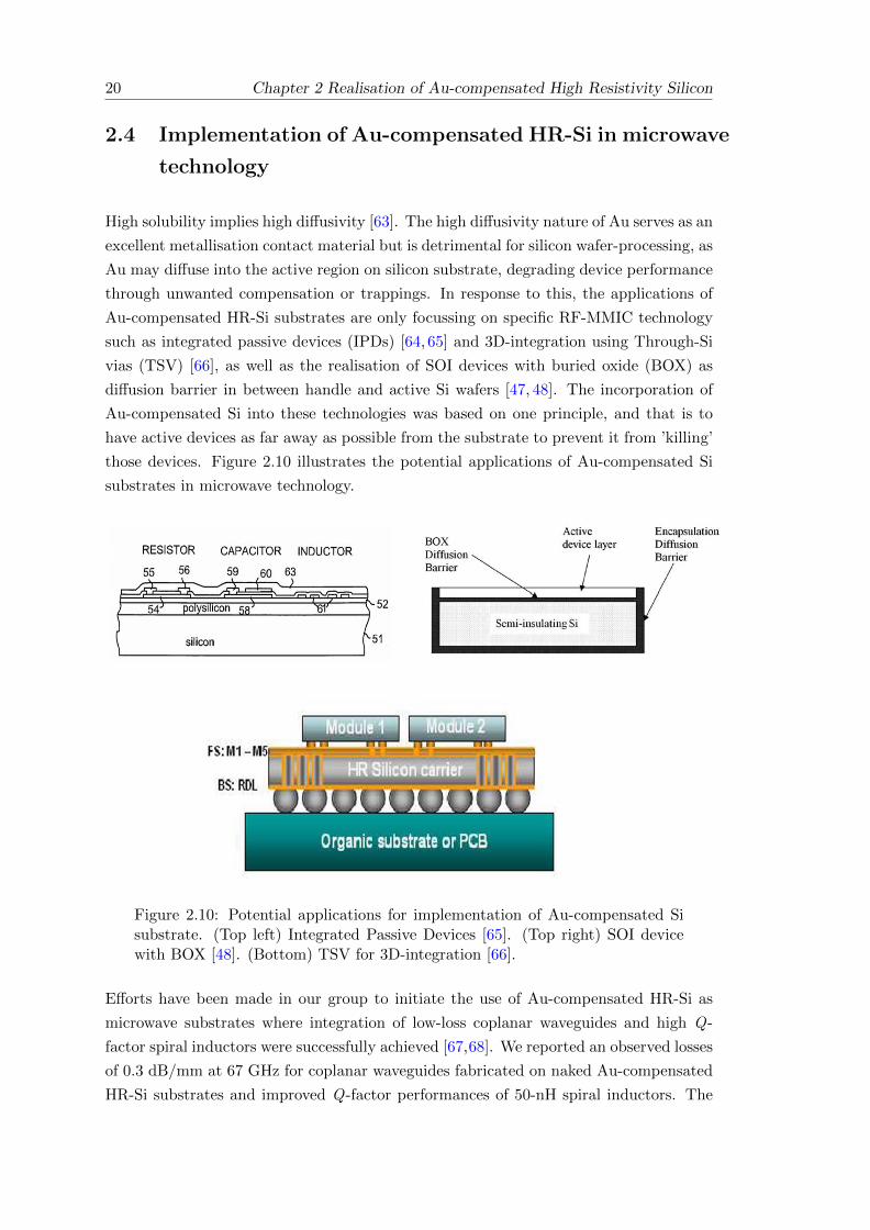
those devices. Figure 2.10 illustrates the potential applications of Au-compensated Si
substrates in microwave technology.
Figure 2.10: Potential applications for implementation of Au-compensated Sisubstrate. (Top left) Integrated Passive Devices [65]. (Top right) SOI devicewith BOX [48]. (Bottom) TSV for 3D-integration [66].
Efforts have been made in our group to initiate the use of Au-compensated HR-Si as
microwave substrates where integration of low-loss coplanar waveguides and high Q-
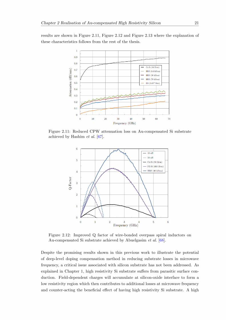
factor spiral inductors were successfully achieved [67,68]. We reported an observed losses
of 0.3 dB/mm at 67 GHz for coplanar waveguides fabricated on naked Au-compensated
HR-Si substrates and improved Q-factor performances of 50-nH spiral inductors. The
Chapter 2 Realisation of Au-compensated High Resistivity Silicon 21
results are shown in Figure 2.11, Figure 2.12 and Figure 2.13 where the explanation of
these characteristics follows from the rest of the thesis.
Figure 2.11: Reduced CPW attenuation loss on Au-compensated Si substrateachieved by Hashim et al. [67].
Figure 2.12: Improved Q factor of wire-bonded overpass spiral inductors onAu-compensated Si substrate achieved by Abuelgasim et al. [68].
Despite the promising results shown in this previous work to illustrate the potential
of deep-level doping compensation method in reducing substrate losses in microwave
frequency, a critical issue associated with silicon substrate has not been addressed. As
explained in Chapter 1, high resistivity Si substrate suffers from parasitic surface con-
duction. Field-dependent charges will accumulate at silicon-oxide interface to form a
low resistivity region which then contributes to additional losses at microwave frequency
and counter-acting the beneficial effect of having high resistivity Si substrate. A high
22 Chapter 2 Realisation of Au-compensated High Resistivity Silicon
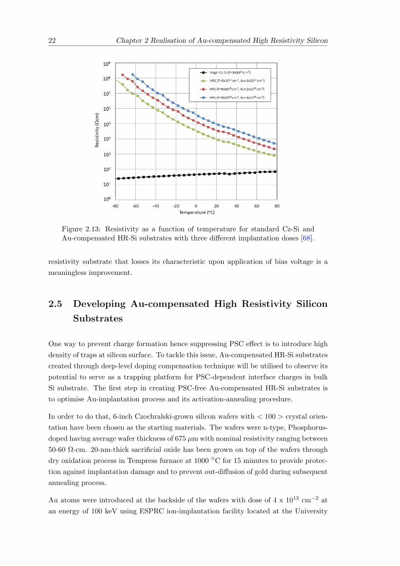
Figure 2.13: Resistivity as a function of temperature for standard Cz-Si andAu-compensated HR-Si substrates with three different implantation doses [68].
resistivity substrate that losses its characteristic upon application of bias voltage is a
meaningless improvement.
2.5 Developing Au-compensated High Resistivity Silicon
Substrates
One way to prevent charge formation hence suppressing PSC effect is to introduce high
density of traps at silicon surface. To tackle this issue, Au-compensated HR-Si substrates
created through deep-level doping compensation technique will be utilised to observe its
potential to serve as a trapping platform for PSC-dependent interface charges in bulk
Si substrate. The first step in creating PSC-free Au-compensated HR-Si substrates is
to optimise Au-implantation process and its activation-annealing procedure.
In order to do that, 6-inch Czochralski-grown silicon wafers with < 100 > crystal orien-
tation have been chosen as the starting materials. The wafers were n-type, Phosphorus-
doped having average wafer thickness of 675 µm with nominal resistivity ranging between
50-60 Ω-cm. 20-nm-thick sacrificial oxide has been grown on top of the wafers through
dry oxidation process in Tempress furnace at 1000 C for 15 minutes to provide protec-
tion against implantation damage and to prevent out-diffusion of gold during subsequent
annealing process.
Au atoms were introduced at the backside of the wafers with dose of 4 x 1013 cm−2 at
an energy of 100 keV using ESPRC ion-implantation facility located at the University
Chapter 2 Realisation of Au-compensated High Resistivity Silicon 23
of Surrey. Once implanted, the wafers were treated under annealing condition of 950 Cfor 1 hour in Argon environment to activate the Au dopants. The implantation details
and annealing temperature were optimised values obtained in [68]. Accordingly, the
combination of this particular implantation dose and annealing temperature provides
the highest resistivity enhancement.
0 5 0 1 0 0 1 5 0 2 0 0 2 5 0 3 0 00
2 0 0
4 0 0
6 0 0
8 0 0
1 0 0 0
Q u e n c h i n g
Temp
eratur
e (0 C)
T i m e ( m i n )
S l o w - c o o l i n g Q u e n c h i n g
U n l o a d w a f e r
U n l o a d w a f e r
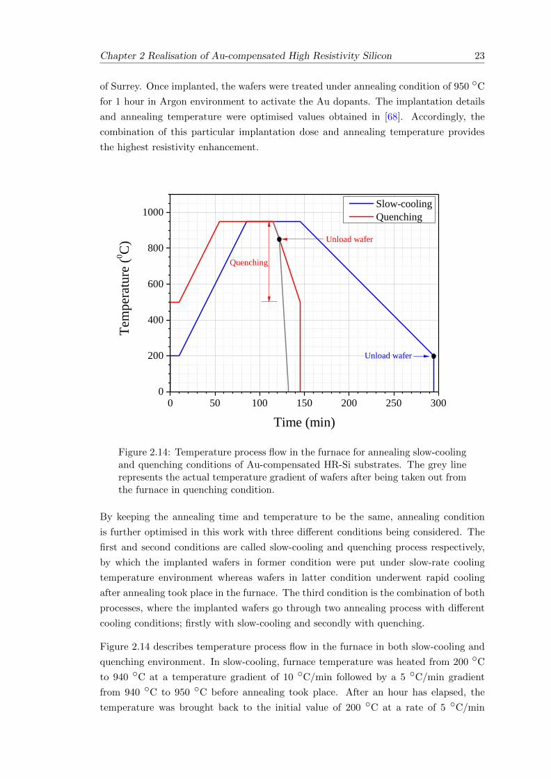
Figure 2.14: Temperature process flow in the furnace for annealing slow-coolingand quenching conditions of Au-compensated HR-Si substrates. The grey linerepresents the actual temperature gradient of wafers after being taken out fromthe furnace in quenching condition.
By keeping the annealing time and temperature to be the same, annealing condition
is further optimised in this work with three different conditions being considered. The
first and second conditions are called slow-cooling and quenching process respectively,
by which the implanted wafers in former condition were put under slow-rate cooling
temperature environment whereas wafers in latter condition underwent rapid cooling
after annealing took place in the furnace. The third condition is the combination of both
processes, where the implanted wafers go through two annealing process with different
cooling conditions; firstly with slow-cooling and secondly with quenching.
Figure 2.14 describes temperature process flow in the furnace in both slow-cooling and
quenching environment. In slow-cooling, furnace temperature was heated from 200 Cto 940 C at a temperature gradient of 10 C/min followed by a 5 C/min gradient
from 940 C to 950 C before annealing took place. After an hour has elapsed, the
temperature was brought back to the initial value of 200 C at a rate of 5 C/min
24 Chapter 2 Realisation of Au-compensated High Resistivity Silicon
all the way down. In the quenching process, the heating procedure was identical to
the one in slow-cooling until annealing took place. After annealing completed, furnace
temperature was brought down at a rate of 15 C/min with the wafers taken out at 850C to assist the quenching process.
After annealing took place, the sacrificial oxide grown earlier was removed through wet-
etching in buffered 20:1 hydrofluoric acid (HF) until hydrophobic. The chemical reaction
involved:
SiO2(s) + 6HF (aq)→ H2SiOF6(aq) + 2H2O(aq) (2.11)
Once oxide was removed, four-point-probe measurement was conducted to find the resis-
tivity of the wafers. The reason for this immediate action was to ensure good electrical
contact between the probe and the substrate, right before native oxide started to grow
on the silicon. A Jandel RM3-AR four-point-prober was used to measure sheet resis-
tance at the front and the back of each wafer at five different points, covering the whole
surface area. The values were then averaged and multiplied by average wafer thickness
of 675 µm to find the resistivity of front side and backside of the wafers.
Table 2.2 shows the difference in resistivity enhancement measured for these three dif-
ferent conditions. First of all, it is evident that the resistivity at the front of the wafer
reflects the resistivity at the back indicating that the kick-out diffusion mechanism is
present. Also can be seen from the table, the highest resistivity enhancement was ob-
tained from the combination of both slow-cooling and quenching annealing conditions.
To explain this matter further, this process will be broken down into two individual
annealing condition, first being slow-cooling then followed by quenching.
In slow-cooling, interstitial Au atoms start to diffuse after T = 600 C into Si crystals
before substituting for Si self-interstitials at temperature above 800 C. This is when the
resistivity starts to change and substitutional Au atoms are compensating for the free
carriers and thermal donors to increase bulk resistivity of Si. However, maximum com-
pensation only occurs during the one-hour annealing at 950 C, the highest temperature
reached during the whole procedure. When the cooling process starts, temperature is
brought down to initial value of 200 C at a very slow rate. This causes some of the Au
atoms to give up their substitutional positions and de-compensate, reducing the resis-
tivity. Not only that, a generation of thermal donors might also contribute to resistivity
reduction when furnace cools down below 500 C. Having said that, resistivity does not
reach its undoped value (shown by resistivity of 1-2 kΩ-cm measured in slow-cooling
condition in Table 2.2), indicating that the remaining substitutional Au atoms are still
electrically active and able to compensate.
In the quenching process, the substitutional Au atoms do not have enough time to
decompensate and so, will remain in their substitutional positions until after the wafers
Chapter 2 Realisation of Au-compensated High Resistivity Silicon 25
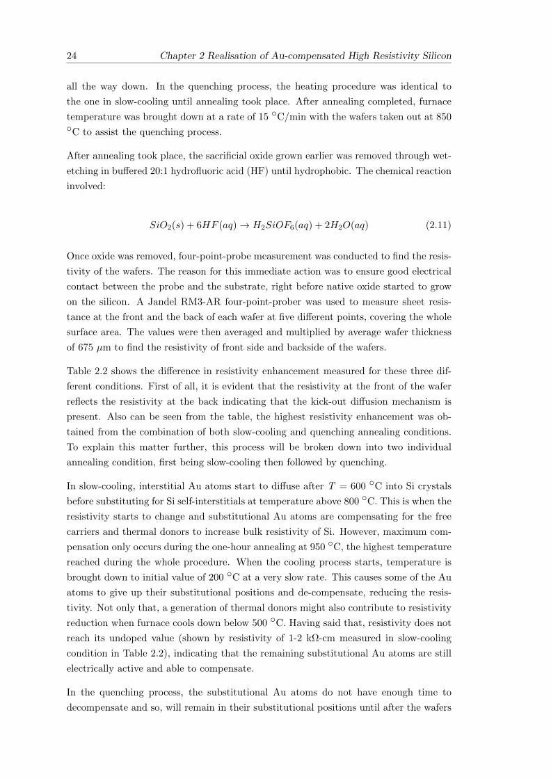
Annealing Procedure Resistivity (kΩ-cm)FRONT BACK
Slow-cooling 1.54 2.00
Quenching 22.6 21.7
Slow-cooling + Quenching 37.0 32.0
Table 2.2: Four-point-probe resistivity measurement result for wafers underwentslow-cooling, quenching or both before Au layer removal through wet-etching.Measurements were conducted at the front and the back sides of the wafers withpristine resistivity value of 50-60 Ω-cm.
were unloaded at 850 C. Unloading the wafers at this temperature also prevents the
generation of thermal donors, which will provide the wafers with significant increase in
resistivity due to full compensation at 950 C.
In the third condition where both processes were combined, implanted wafers were pro-
vided with a so-called ’elevated threshold’ before going through second annealing proce-
dure involving quenching. The slightly enhanced resistivity obtained from slow-cooling
was brought into quenching environment to serve as threshold resistivity before second
annealing took place. As a result, more Au atoms get compensated and give rise to
higher resistivity. Based on these observations, it was decided to proceed with combined
annealing condition for all further processed wafers.
Subsequent to the removal of the sacrificial oxide and the resistivity measurements, a
Au-surface etch was performed to remove any potential conductive layer due to an excess
of Au. The surface etch was performed through wet-etching using gold etchant with a
mixing ratio of KI : I2 : H2O = 4g : 1g : 40g for a duration of 1 minute. The reaction
that has taken place was:
2Au(s) + I2(aq)→ 2AuI(aq) (2.12)
Once the residual Au had been removed from the wafers, resistivity of the wafers were
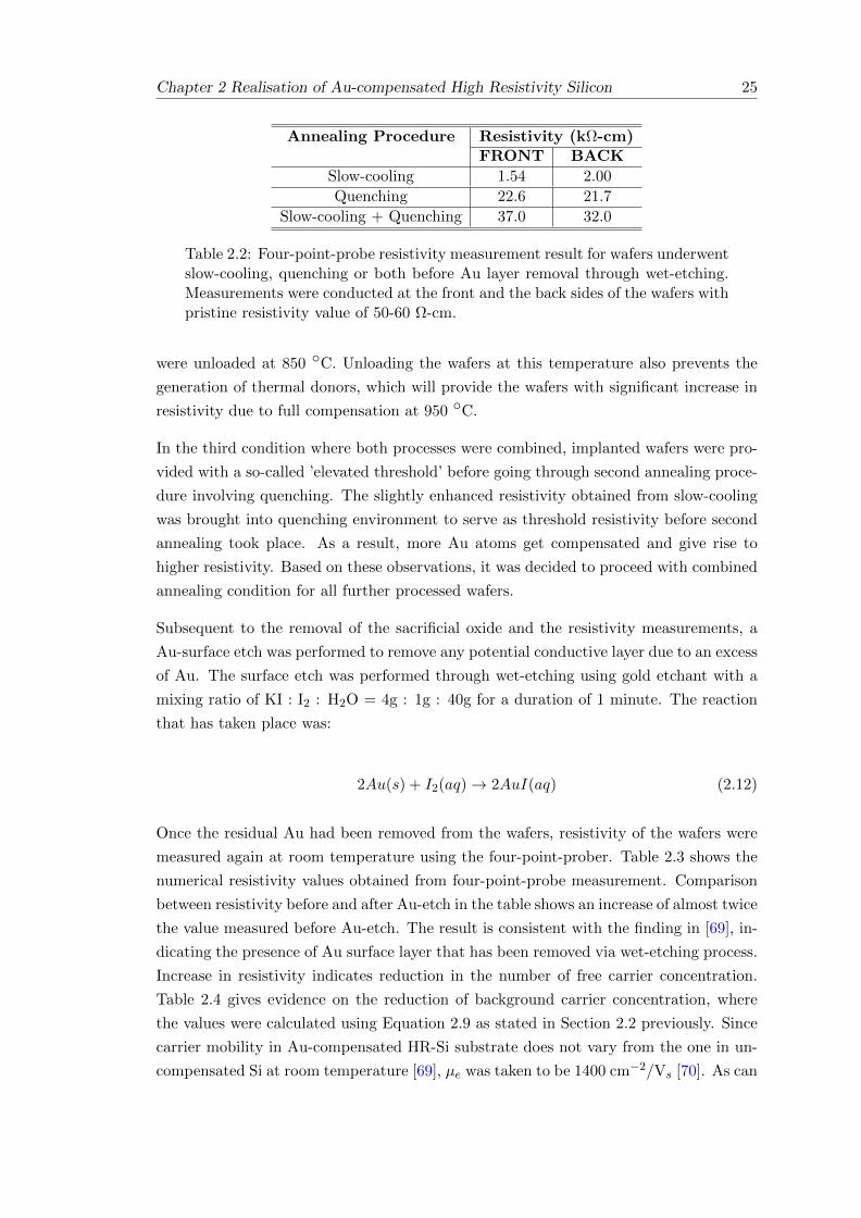
measured again at room temperature using the four-point-prober. Table 2.3 shows the
numerical resistivity values obtained from four-point-probe measurement. Comparison
between resistivity before and after Au-etch in the table shows an increase of almost twice
the value measured before Au-etch. The result is consistent with the finding in [69], in-
dicating the presence of Au surface layer that has been removed via wet-etching process.
Increase in resistivity indicates reduction in the number of free carrier concentration.
Table 2.4 gives evidence on the reduction of background carrier concentration, where
the values were calculated using Equation 2.9 as stated in Section 2.2 previously. Since
carrier mobility in Au-compensated HR-Si substrate does not vary from the one in un-
compensated Si at room temperature [69], µe was taken to be 1400 cm−2/Vs [70]. As can
26 Chapter 2 Realisation of Au-compensated High Resistivity Silicon
Wafer Resistivity (kΩ-cm)FRONT BACK
Before After Before After
1 43.2 74.9 37.9 75.62 44.8 75.9 39.8 73.93 41.6 79.9 33.7 78.84 24.0 44.4 22.8 43.75 23.3 42.8 22.3 43.06 28.7 40.6 30.1 40.3
MEAN 34.3 60.0 31.1 60.0
STANDARD DEVIATION 10.0 18.9 7.43 18.6
Table 2.3: Four-point-probe resistivity values measured at the front and theback sides of Au-compensated HR-Si substrates developed through combinedannealing procedures. Results include measurements done before and after Au-etching.
Substrate Type Etching ρ (kΩ−cm) n (cm−3)
Au-compensated HR-Si Au-etched 60.0 6.0 x 10¹⁰
Au-compensated HR-Si − 35.0 2.0 x 10¹¹
Float-Zone N/A 0.36 1.2x10¹³
Table 2.4: Calculated free carrier concentrations in Au-compensated HR-Si sub-strates and Float-zone Si substrates using Equation 2.9.
be seen from the table, majority carrier concentrations are comparatively lower in Au-
compensated Si substrates compared to Float-zone Si substrate, where a reduction close
to a power of three can be observed in Au-etched, Au-compensated HR-Si substrate.
The value approaches the level of intrinsic Si, as mentioned in Section 2.1.
2.6 Summary
Deep-level doping compensation method is used to create high resistivity Si substrates.
Au was implanted into 50 Ω-cm Czochralski-Si substrates at the backside of the sub-
strates with a dose of 4 x 1013 cm−2 at an energy of 100 keV. The implanted substrates
were then put under three different annealing procedures with the annealing treatment
kept at a temperature of 950 C for one hour. The highest increase in resistivity is seen
for substrates that underwent combined annealing procedure consisting of slow cooling
and quenching, indicating the importance of slow-cooling process to act as an ’elevated
threshold’ for subsequent quenching process in the annealing treatment. Au-etching
provides an additional increase in resistivity, due to removal of an inactive Au surface
layer on Si surface. The highest recorded resistivity is seen for Au-compensated HR-Si
substrates developed through combined annealing procedure with Au-etching effect with
a typical value of 60 kΩ-cm and a maximum value of 80 kΩ-cm.
Chapter 3
Design and Fabrication of
Microwave Devices
Parasitic surface conduction on Au-compensated Si-based microwave devices were evalu-
ated and quantified using metal-oxide-silicon structures. Three types of devices were de-
signed and fabricated in this work; capacitors, coplanar waveguides and meander induc-
tors with the incorporation of back metallisation of the structure to allow back-biasing
of devices during electrical and microwave characterisations. Electrical characterisations
on capacitor structure were used to evaluate surface charge effects in Au-compensated
HR-Si whereas microwave characterisations on coplanar waveguides and meander induc-
tors were useful for observing the potential suppression of parasitic surface conduction
using this type of substrate.
3.1 Capacitor design
Square-shaped capacitors were designed. Eight different sizes of capacitors were included
to observe its scaling property with respect to area. Apart from lithography checking,
the significance of analysing this property is to enable the extraction of oxide thickness,
tox from oxide capacitance, Cox equation given by:
Cox =εoεrA
tox(3.1)
where εo and εr are permittivity of free-space and relative permittivity of SiO2 respec-
tively, and A is the capacitance area. Table 3.1 summarises the set of capacitors designed
in this work and their corresponding patterns are shown in Figure 3.1.
27
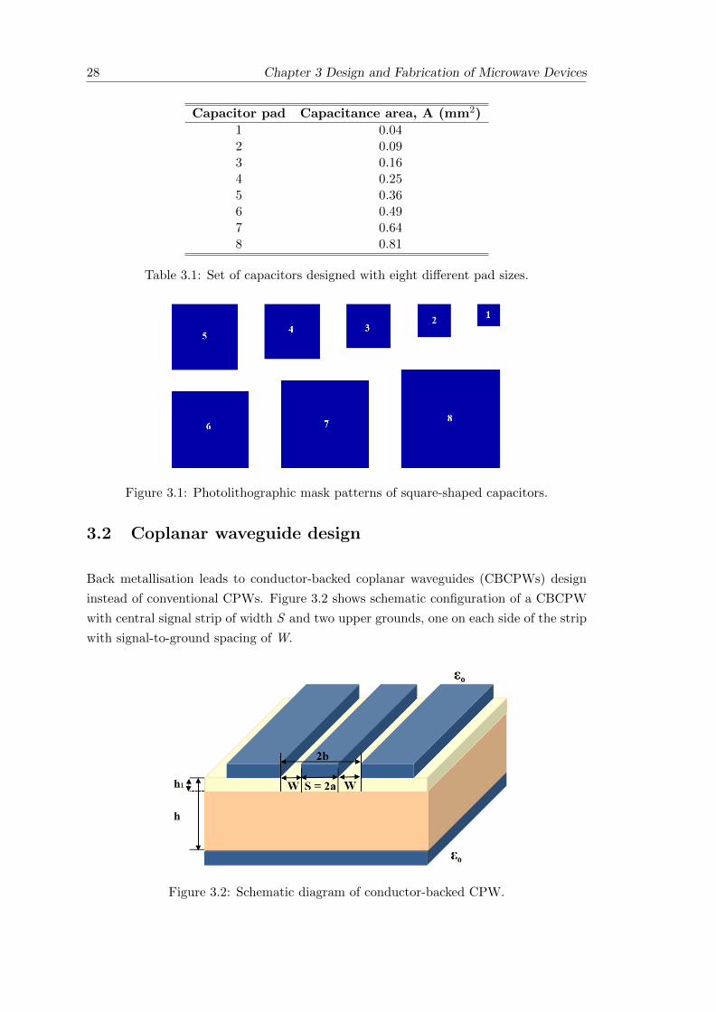
28 Chapter 3 Design and Fabrication of Microwave Devices
Capacitor pad Capacitance area, A (mm2)
1 0.042 0.093 0.164 0.255 0.366 0.497 0.648 0.81
Table 3.1: Set of capacitors designed with eight different pad sizes.
Figure 3.1: Photolithographic mask patterns of square-shaped capacitors.
3.2 Coplanar waveguide design
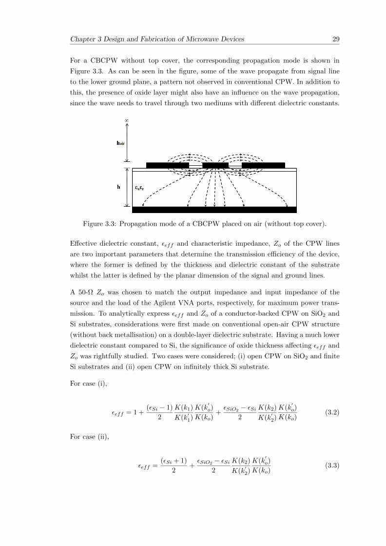
Back metallisation leads to conductor-backed coplanar waveguides (CBCPWs) design
instead of conventional CPWs. Figure 3.2 shows schematic configuration of a CBCPW
with central signal strip of width S and two upper grounds, one on each side of the strip
with signal-to-ground spacing of W.
Figure 3.2: Schematic diagram of conductor-backed CPW.
Chapter 3 Design and Fabrication of Microwave Devices 29
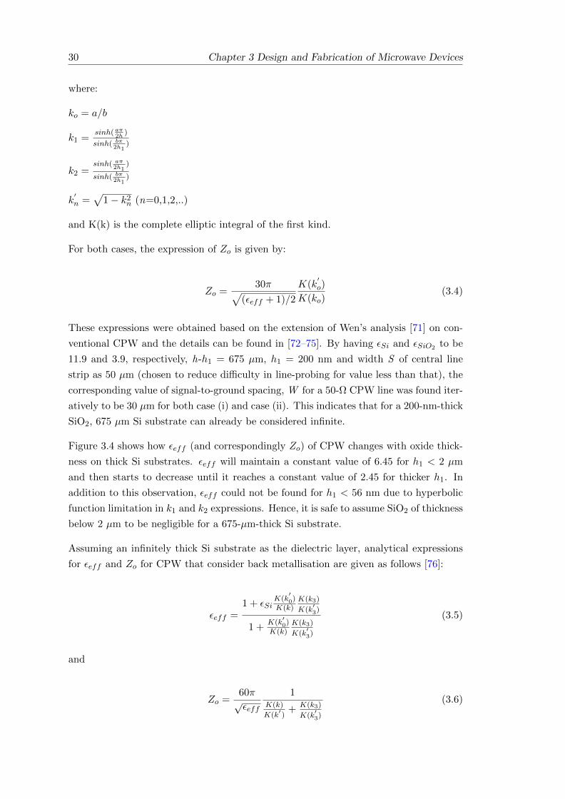
For a CBCPW without top cover, the corresponding propagation mode is shown in
Figure 3.3. As can be seen in the figure, some of the wave propagate from signal line
to the lower ground plane, a pattern not observed in conventional CPW. In addition to
this, the presence of oxide layer might also have an influence on the wave propagation,
since the wave needs to travel through two mediums with different dielectric constants.
Figure 3.3: Propagation mode of a CBCPW placed on air (without top cover).
Effective dielectric constant, εeff and characteristic impedance, Zo of the CPW lines
are two important parameters that determine the transmission efficiency of the device,
where the former is defined by the thickness and dielectric constant of the substrate
whilst the latter is defined by the planar dimension of the signal and ground lines.
A 50-Ω Zo was chosen to match the output impedance and input impedance of the
source and the load of the Agilent VNA ports, respectively, for maximum power trans-
mission. To analytically express εeff and Zo of a conductor-backed CPW on SiO2 and
Si substrates, considerations were first made on conventional open-air CPW structure
(without back metallisation) on a double-layer dielectric substrate. Having a much lower
dielectric constant compared to Si, the significance of oxide thickness affecting εeff and
Zo was rightfully studied. Two cases were considered; (i) open CPW on SiO2 and finite
Si substrates and (ii) open CPW on infinitely thick Si substrate.
For case (i),
εeff = 1 +(εSi − 1)
2
K(k1)
K(k′1)
K(k′o)
K(ko)+εSiO2 − εSi
2
K(k2)
K(k′2)
K(k′o)
K(ko)(3.2)
For case (ii),
εeff =(εSi + 1)
2+εSiO2 − εSi
2
K(k2)
K(k′2)
K(k′o)
K(ko)(3.3)
30 Chapter 3 Design and Fabrication of Microwave Devices
where:
ko = a/b
k1 =sinh(aπ
2h)
sinh( bπ2h1
)
k2 =sinh( aπ
2h1)
sinh( bπ2h1
)
k′n =
√1− k2n (n=0,1,2,..)
and K(k) is the complete elliptic integral of the first kind.
For both cases, the expression of Zo is given by:
Zo =30π√
(εeff + 1)/2
K(k′o)
K(ko)(3.4)
These expressions were obtained based on the extension of Wen’s analysis [71] on con-
ventional CPW and the details can be found in [72–75]. By having εSi and εSiO2 to be
11.9 and 3.9, respectively, h-h1 = 675 µm, h1 = 200 nm and width S of central line
strip as 50 µm (chosen to reduce difficulty in line-probing for value less than that), the
corresponding value of signal-to-ground spacing, W for a 50-Ω CPW line was found iter-
atively to be 30 µm for both case (i) and case (ii). This indicates that for a 200-nm-thick
SiO2, 675 µm Si substrate can already be considered infinite.
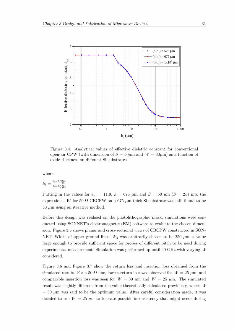
Figure 3.4 shows how εeff (and correspondingly Zo) of CPW changes with oxide thick-
ness on thick Si substrates. εeff will maintain a constant value of 6.45 for h1 < 2 µm
and then starts to decrease until it reaches a constant value of 2.45 for thicker h1. In
addition to this observation, εeff could not be found for h1 < 56 nm due to hyperbolic
function limitation in k1 and k2 expressions. Hence, it is safe to assume SiO2 of thickness
below 2 µm to be negligible for a 675-µm-thick Si substrate.
Assuming an infinitely thick Si substrate as the dielectric layer, analytical expressions
for εeff and Zo for CPW that consider back metallisation are given as follows [76]:
εeff =1 + εSi
K(k′0)
K(k)K(k3)
K(k′3)
1 +K(k
′0)
K(k)K(k3)
K(k′3)
(3.5)
and
Zo =60π√εeff
1K(k)
K(k′ )+ K(k3)
K(k′3)
(3.6)
Chapter 3 Design and Fabrication of Microwave Devices 31
0 . 1 1 1 0 1 0 0 1 0 0 02
3
4
5
6
7 ( h - h 1 ) = 5 2 5 µm ( h - h 1 ) = 6 7 5 µm ( h - h 1 ) = 1 x 1 0 9 µm
Effect
ive di
electr
ic cons
tant, ε
eff
h 1 ( µm )
Figure 3.4: Analytical values of effective dieletric constant for conventionalopen-air CPW (with dimension of S = 50µm and W = 30µm) as a function ofoxide thickness on different Si substrates.
where:
k3 =tanh(aπ
2h)
tanh( bπ2h
)
Putting in the values for εSi = 11.9, h = 675 µm and S = 50 µm (S = 2a) into the
expressions, W for 50-Ω CBCPW on a 675-µm-thick Si substrate was still found to be
30 µm using an iterative method.
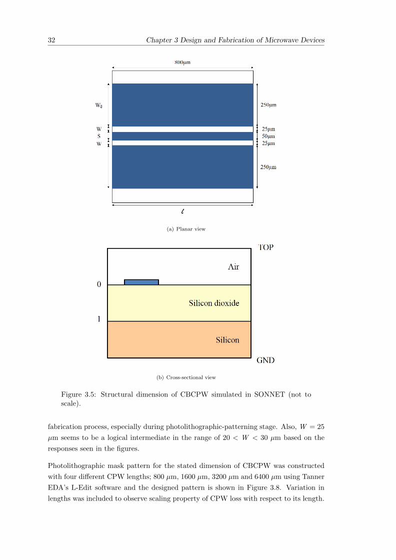
Before this design was realised on the photolithographic mask, simulations were con-
ducted using SONNET’s electromagnetic (EM) software to evaluate the chosen dimen-
sion. Figure 3.5 shows planar and cross-sectional views of CBCPW constructed in SON-
NET. Width of upper ground lines, Wg was arbitrarily chosen to be 250 µm, a value
large enough to provide sufficient space for probes of different pitch to be used during
experimental measurement. Simulation was performed up until 40 GHz with varying W
considered.
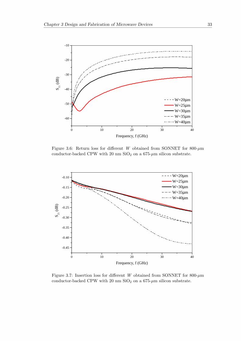
Figure 3.6 and Figure 3.7 show the return loss and insertion loss obtained from the
simulated results. For a 50-Ω line, lowest return loss was observed for W = 25 µm, and
comparable insertion loss was seen for W = 30 µm and W = 25 µm. The simulated
result was slightly different from the value theoretically calculated previously, where W
= 30 µm was said to be the optimum value. After careful consideration made, it was
decided to use W = 25 µm to tolerate possible inconsistency that might occur during
32 Chapter 3 Design and Fabrication of Microwave Devices
(a) Planar view
(b) Cross-sectional view
Figure 3.5: Structural dimension of CBCPW simulated in SONNET (not toscale).
fabrication process, especially during photolithographic-patterning stage. Also, W = 25
µm seems to be a logical intermediate in the range of 20 < W < 30 µm based on the
responses seen in the figures.
Photolithographic mask pattern for the stated dimension of CBCPW was constructed
with four different CPW lengths; 800 µm, 1600 µm, 3200 µm and 6400 µm using Tanner
EDA’s L-Edit software and the designed pattern is shown in Figure 3.8. Variation in
lengths was included to observe scaling property of CPW loss with respect to its length.
Chapter 3 Design and Fabrication of Microwave Devices 33
0 1 0 2 0 3 0 4 0
- 6 0
- 5 0
- 4 0
- 3 0
- 2 0
- 1 0
S 11 (dB
)
F r e q u e n c y , f ( G H z )
W = 2 0 µm W = 2 5 µm W = 3 0 µm W = 3 5 µm W = 4 0 µm
Figure 3.6: Return loss for different W obtained from SONNET for 800-µmconductor-backed CPW with 20 nm SiO2 on a 675-µm silicon substrate.
0 1 0 2 0 3 0 4 0
- 0 . 4 5
- 0 . 4 0
- 0 . 3 5
- 0 . 3 0
- 0 . 2 5
- 0 . 2 0
- 0 . 1 5
- 0 . 1 0
S 21 (dB
)
F r e q u e n c y , f ( G H z )
W = 2 0 µm W = 2 5 µm W = 3 0 µm W = 3 5 µm W = 4 0 µm
Figure 3.7: Insertion loss for different W obtained from SONNET for 800-µmconductor-backed CPW with 20 nm SiO2 on a 675-µm silicon substrate.
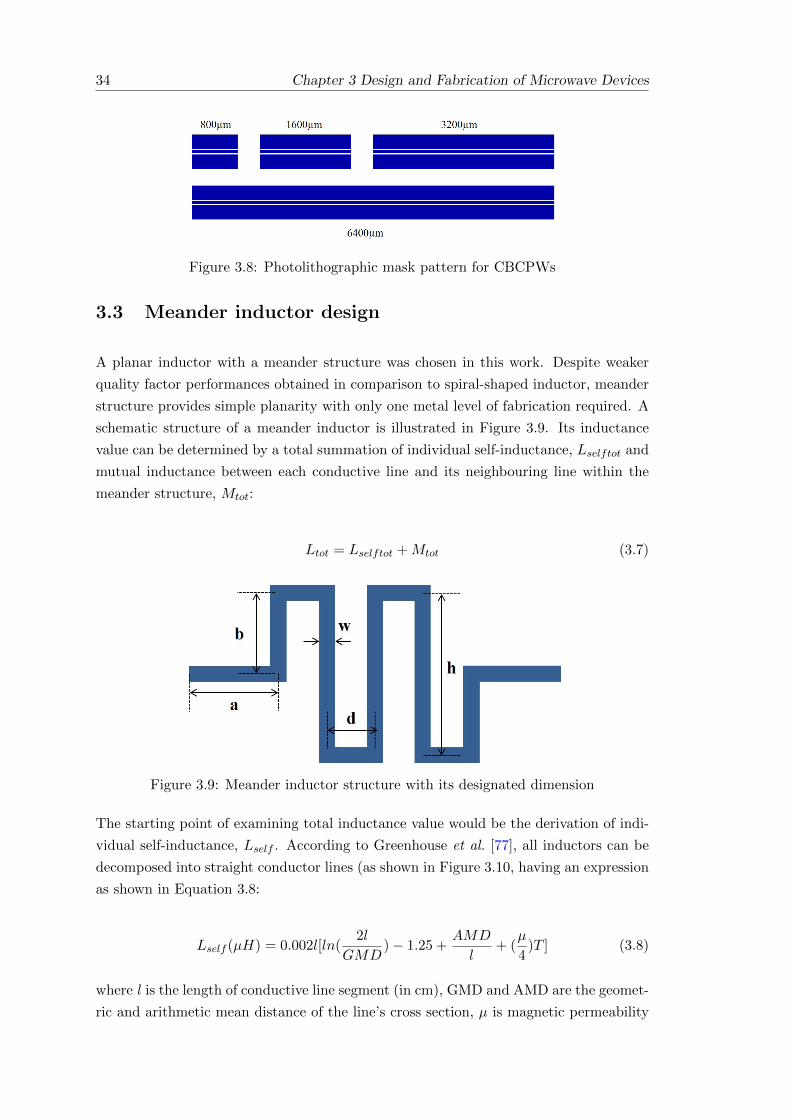
34 Chapter 3 Design and Fabrication of Microwave Devices
Figure 3.8: Photolithographic mask pattern for CBCPWs
3.3 Meander inductor design
A planar inductor with a meander structure was chosen in this work. Despite weaker
quality factor performances obtained in comparison to spiral-shaped inductor, meander
structure provides simple planarity with only one metal level of fabrication required. A
schematic structure of a meander inductor is illustrated in Figure 3.9. Its inductance
value can be determined by a total summation of individual self-inductance, Lselftot and
mutual inductance between each conductive line and its neighbouring line within the
meander structure, Mtot:
Ltot = Lselftot +Mtot (3.7)
Figure 3.9: Meander inductor structure with its designated dimension
The starting point of examining total inductance value would be the derivation of indi-
vidual self-inductance, Lself . According to Greenhouse et al. [77], all inductors can be
decomposed into straight conductor lines (as shown in Figure 3.10, having an expression
as shown in Equation 3.8:
Lself (µH) = 0.002l[ln(2l
GMD)− 1.25 +
AMD
l+ (
µ
4)T ] (3.8)
where l is the length of conductive line segment (in cm), GMD and AMD are the geomet-
ric and arithmetic mean distance of the line’s cross section, µ is magnetic permeability
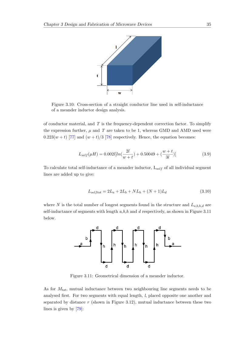
Chapter 3 Design and Fabrication of Microwave Devices 35
Figure 3.10: Cross-section of a straight conductor line used in self-inductanceof a meander inductor design analysis.
of conductor material, and T is the frequency-dependent correction factor. To simplify
the expression further, µ and T are taken to be 1, whereas GMD and AMD used were
0.223(w + t) [77] and (w + t)/3 [78] respectively. Hence, the equation becomes:
Lself (µH) = 0.002l[ln(2l
w + t) + 0.50049 + (
w + t
3l)] (3.9)
To calculate total self-inductance of a meander inductor, Lself of all individual segment
lines are added up to give:
Lselftot = 2La + 2Lb +NLh + (N + 1)Ld (3.10)
where N is the total number of longest segments found in the structure and La,b,h,d are
self-inductance of segments with length a,b,h and d respectively, as shown in Figure 3.11
below.
Figure 3.11: Geometrical dimension of a meander inductor.
As for Mtot, mutual inductance between two neighbouring line segments needs to be
analysed first. For two segments with equal length, l, placed opposite one another and
separated by distance r (shown in Figure 3.12), mutual inductance between these two
lines is given by [79]:
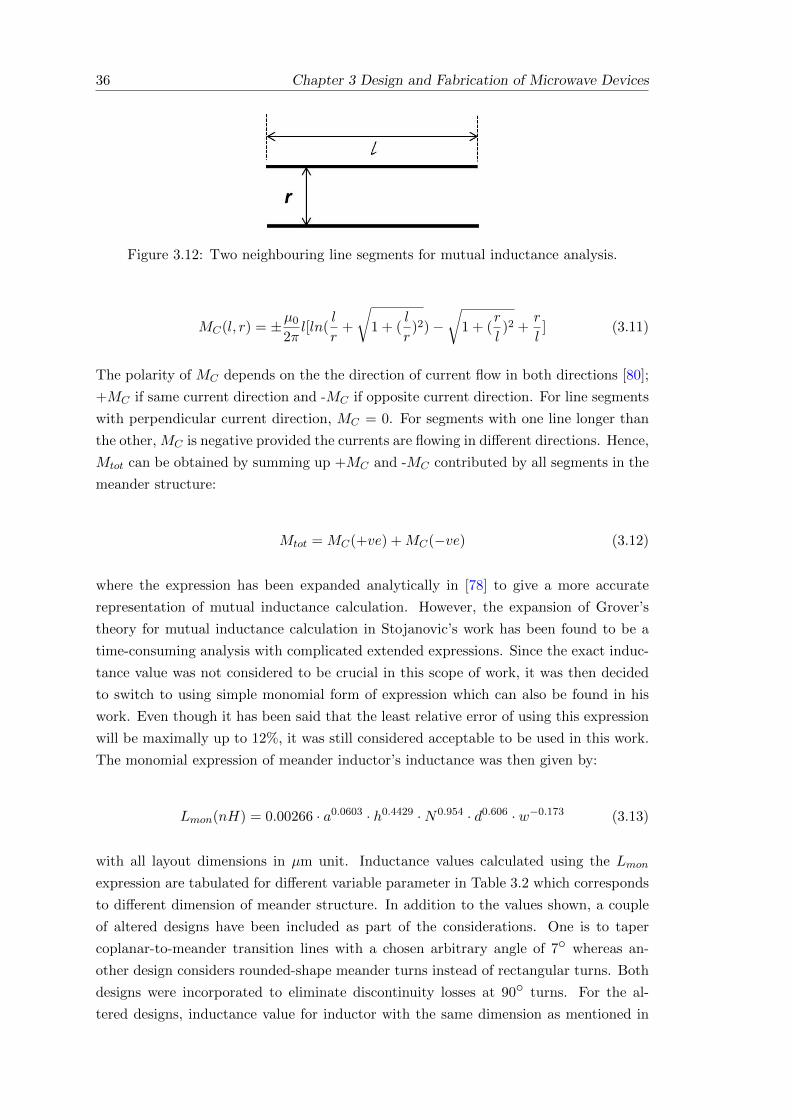
36 Chapter 3 Design and Fabrication of Microwave Devices
Figure 3.12: Two neighbouring line segments for mutual inductance analysis.
MC(l, r) = ±µ02πl[ln(
l
r+
√1 + (
l
r)2)−
√1 + (
r
l)2 +
r
l] (3.11)
The polarity of MC depends on the the direction of current flow in both directions [80];
+MC if same current direction and -MC if opposite current direction. For line segments
with perpendicular current direction, MC = 0. For segments with one line longer than
the other, MC is negative provided the currents are flowing in different directions. Hence,
Mtot can be obtained by summing up +MC and -MC contributed by all segments in the
meander structure:
Mtot = MC(+ve) +MC(−ve) (3.12)
where the expression has been expanded analytically in [78] to give a more accurate
representation of mutual inductance calculation. However, the expansion of Grover’s
theory for mutual inductance calculation in Stojanovic’s work has been found to be a
time-consuming analysis with complicated extended expressions. Since the exact induc-
tance value was not considered to be crucial in this scope of work, it was then decided
to switch to using simple monomial form of expression which can also be found in his
work. Even though it has been said that the least relative error of using this expression
will be maximally up to 12%, it was still considered acceptable to be used in this work.
The monomial expression of meander inductor’s inductance was then given by:
Lmon(nH) = 0.00266 · a0.0603 · h0.4429 ·N0.954 · d0.606 · w−0.173 (3.13)
with all layout dimensions in µm unit. Inductance values calculated using the Lmon
expression are tabulated for different variable parameter in Table 3.2 which corresponds
to different dimension of meander structure. In addition to the values shown, a couple
of altered designs have been included as part of the considerations. One is to taper
coplanar-to-meander transition lines with a chosen arbitrary angle of 7 whereas an-
other design considers rounded-shape meander turns instead of rectangular turns. Both
designs were incorporated to eliminate discontinuity losses at 90 turns. For the al-
tered designs, inductance value for inductor with the same dimension as mentioned in
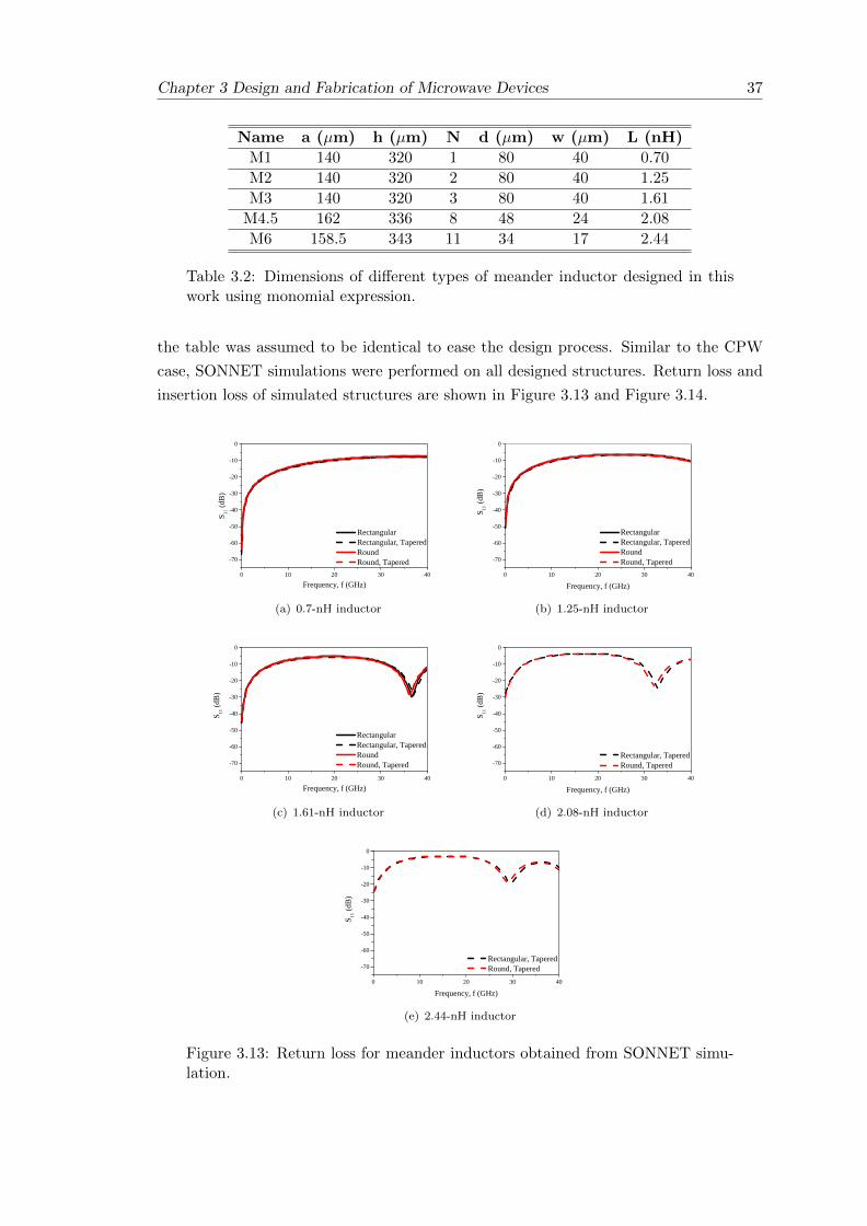
Chapter 3 Design and Fabrication of Microwave Devices 37
Name a (µm) h (µm) N d (µm) w (µm) L (nH)
M1 140 320 1 80 40 0.70
M2 140 320 2 80 40 1.25
M3 140 320 3 80 40 1.61
M4.5 162 336 8 48 24 2.08
M6 158.5 343 11 34 17 2.44
Table 3.2: Dimensions of different types of meander inductor designed in thiswork using monomial expression.
the table was assumed to be identical to ease the design process. Similar to the CPW
case, SONNET simulations were performed on all designed structures. Return loss and
insertion loss of simulated structures are shown in Figure 3.13 and Figure 3.14.
0 1 0 2 0 3 0 4 0- 7 0
- 6 0
- 5 0
- 4 0
- 3 0
- 2 0
- 1 0
0
S 11 (dB
)
F r e q u e n c y , f ( G H z )
R e c t a n g u l a r R e c t a n g u l a r , T a p e r e d R o u n d R o u n d , T a p e r e d
(a) 0.7-nH inductor
0 1 0 2 0 3 0 4 0- 7 0
- 6 0
- 5 0
- 4 0
- 3 0
- 2 0
- 1 0
0
S 11 (dB
)
F r e q u e n c y , f ( G H z )
R e c t a n g u l a r R e c t a n g u l a r , T a p e r e d R o u n d R o u n d , T a p e r e d
(b) 1.25-nH inductor
0 1 0 2 0 3 0 4 0- 7 0
- 6 0
- 5 0
- 4 0
- 3 0
- 2 0
- 1 0
0
S 11 (dB
)
F r e q u e n c y , f ( G H z )
R e c t a n g u l a r R e c t a n g u l a r , T a p e r e d R o u n d R o u n d , T a p e r e d
(c) 1.61-nH inductor
0 1 0 2 0 3 0 4 0- 7 0
- 6 0
- 5 0
- 4 0
- 3 0
- 2 0
- 1 0
0
S 11 (dB
)
F r e q u e n c y , f ( G H z )
R e c t a n g u l a r , T a p e r e d R o u n d , T a p e r e d
(d) 2.08-nH inductor
0 1 0 2 0 3 0 4 0- 7 0
- 6 0
- 5 0
- 4 0
- 3 0
- 2 0
- 1 0
0
S 11 (dB
)
F r e q u e n c y , f ( G H z )
R e c t a n g u l a r , T a p e r e d R o u n d , T a p e r e d
(e) 2.44-nH inductor
Figure 3.13: Return loss for meander inductors obtained from SONNET simu-lation.
38 Chapter 3 Design and Fabrication of Microwave Devices
Return loss characteristics of all structures show very high reflection with nearly -5 dB
value seen throughout the whole frequency range, indicating 30% of input power are
being reflected by the devices. However, high rejection is seen for structures with values
≥ 1.61 nH where a bandwidth of 3 GHz is observed for return loss of -20 dB.
In terms of insertion loss, the structures depict inductor’s behaviour where the loss
increases with increasing frequency. As frequency goes up, inductive reactance of the
structures becomes more significant hence translates into higher insertion loss. Never-
theless, for structures with values ≥ 1.61 nH, the loss oscillates at higher frequencies
and reaches a certain bandwidth where the values are at the minimum. The frequency
range at which this behaviour is observed is the same as the one seen in return loss
characteristics shown in Figure 3.13.
0 1 0 2 0 3 0 4 0
- 5
- 4
- 3
- 2
- 1
0
S 21 (dB
)
F r e q u e n c y , f ( G H z )
R e c t a n g u l a r R e c t a n g u l a r , T a p e r e d R o u n d R o u n d , T a p e r e d
(a) 0.7-nH inductor
0 1 0 2 0 3 0 4 0
- 5
- 4
- 3
- 2
- 1
0S 21 (
dB)
F r e q u e n c y , f ( G H z )
R e c t a n g u l a r R e c t a n g u l a r , T a p e r e d R o u n d R o u n d , T a p e r e d
(b) 1.25-nH inductor
0 1 0 2 0 3 0 4 0
- 5
- 4
- 3
- 2
- 1
0
S 21 (dB
)
F r e q u e n c y , f ( G H z )
R e c t a n g u l a r R e c t a n g u l a r , T a p e r e d R o u n d R o u n d , T a p e r e d
(c) 1.61-nH inductor
0 1 0 2 0 3 0 4 0
- 5
- 4
- 3
- 2
- 1
0
R e c t a n g u l a r , T a p e r e d R o u n d , T a p e r e d
S 21 (dB
)
F r e q u e n c y , f ( G H z )
(d) 2.08-nH inductor
0 1 0 2 0 3 0 4 0
- 5
- 4
- 3
- 2
- 1
0
R e c t a n g u l a r , T a p e r e d R o u n d , T a p e r e d
S 21 (dB
)
F r e q u e n c y , f ( G H z )
(e) 2.44-nH inductor
Figure 3.14: Insertion loss for meander inductors obtained from SONNET sim-ulation.
Chapter 3 Design and Fabrication of Microwave Devices 39
The discussed designs were then realised on photolithographic mask and the patterns
are as shown in Figure 3.15 to Figure 3.19.
Figure 3.15: 0.7-nH-inductor (N = 1) with rectangular (top) and round (bot-tom) shapes, having a 90 discontinuity (left) or tapered (right) CPW-to-meander line. (From top LHS) M1, M1T, M1S and M1ST.
Figure 3.16: 1.25-nH-inductor (N = 2) with rectangular (top) and round (bot-tom) shapes, having a 90 discontinuity (left) or tapered (right) CPW-to-meander line. (From top LHS) M2, M2T, M2S and M2ST.
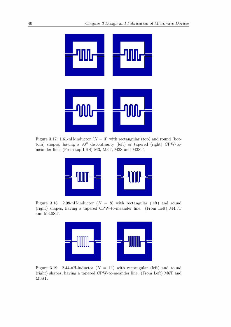
40 Chapter 3 Design and Fabrication of Microwave Devices
Figure 3.17: 1.61-nH-inductor (N = 3) with rectangular (top) and round (bot-tom) shapes, having a 90 discontinuity (left) or tapered (right) CPW-to-meander line. (From top LHS) M3, M3T, M3S and M3ST.
Figure 3.18: 2.08-nH-inductor (N = 8) with rectangular (left) and round(right) shapes, having a tapered CPW-to-meander line. (From Left) M4.5Tand M4.5ST.
Figure 3.19: 2.44-nH-inductor (N = 11) with rectangular (left) and round(right) shapes, having a tapered CPW-to-meander line. (From Left) M6T andM6ST.
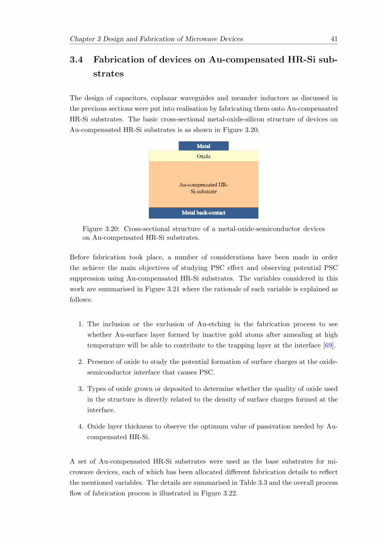
Chapter 3 Design and Fabrication of Microwave Devices 41
3.4 Fabrication of devices on Au-compensated HR-Si sub-
strates
The design of capacitors, coplanar waveguides and meander inductors as discussed in
the previous sections were put into realisation by fabricating them onto Au-compensated
HR-Si substrates. The basic cross-sectional metal-oxide-silicon structure of devices on
Au-compensated HR-Si substrates is as shown in Figure 3.20.
Figure 3.20: Cross-sectional structure of a metal-oxide-semiconductor deviceson Au-compensated HR-Si substrates.
Before fabrication took place, a number of considerations have been made in order
the achieve the main objectives of studying PSC effect and observing potential PSC
suppression using Au-compensated HR-Si substrates. The variables considered in this
work are summarised in Figure 3.21 where the rationale of each variable is explained as
follows:
1. The inclusion or the exclusion of Au-etching in the fabrication process to see
whether Au-surface layer formed by inactive gold atoms after annealing at high
temperature will be able to contribute to the trapping layer at the interface [69].
2. Presence of oxide to study the potential formation of surface charges at the oxide-
semiconductor interface that causes PSC.
3. Types of oxide grown or deposited to determine whether the quality of oxide used
in the structure is directly related to the density of surface charges formed at the
interface.
4. Oxide layer thickness to observe the optimum value of passivation needed by Au-
compensated HR-Si.
A set of Au-compensated HR-Si substrates were used as the base substrates for mi-
crowave devices, each of which has been allocated different fabrication details to reflect
the mentioned variables. The details are summarised in Table 3.3 and the overall process
flow of fabrication process is illustrated in Figure 3.22.
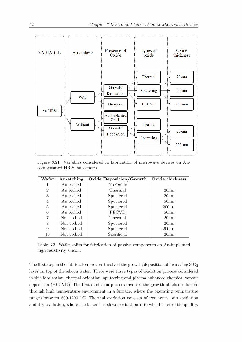
42 Chapter 3 Design and Fabrication of Microwave Devices
Figure 3.21: Variables considered in fabrication of microwave devices on Au-compensated HR-Si substrates.
Wafer Au-etching Oxide Deposition/Growth Oxide thickness
1 Au-etched No Oxide -2 Au-etched Thermal 20nm3 Au-etched Sputtered 20nm4 Au-etched Sputtered 50nm5 Au-etched Sputtered 200nm6 Au-etched PECVD 50nm7 Not etched Thermal 20nm8 Not etched Sputtered 20nm9 Not etched Sputtered 200nm10 Not etched Sacrificial 20nm
Table 3.3: Wafer splits for fabrication of passive components on Au-implantedhigh resistivity silicon.
The first step in the fabrication process involved the growth/deposition of insulating SiO2
layer on top of the silicon wafer. There were three types of oxidation process considered
in this fabrication; thermal oxidation, sputtering and plasma-enhanced chemical vapour
deposition (PECVD). The first oxidation process involves the growth of silicon dioxide
through high temperature environment in a furnace, where the operating temperature
ranges between 800-1200 C. Thermal oxidation consists of two types, wet oxidation
and dry oxidation, where the latter has slower oxidation rate with better oxide quality.
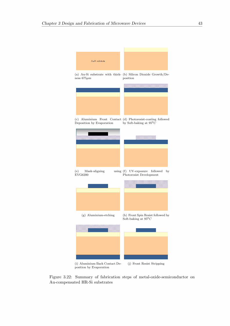
Chapter 3 Design and Fabrication of Microwave Devices 43
(a) Au-Si substrate with thick-ness 675µm
(b) Silicon Dioxide Growth/De-position
(c) Aluminium Front ContactDeposition by Evaporation
(d) Photoresist-coating followedby Soft-baking at 950C
(e) Mask-aligning usingEVG6200
(f) UV-exposure followed byPhotoresist Development
(g) Aluminium-etching (h) Front Spin Resist followed bySoft-baking at 950C
(i) Aluminium Back Contact De-position by Evaporation
(j) Front Resist Stripping
Figure 3.22: Summary of fabrication steps of metal-oxide-semiconductor onAu-compensated HR-Si substrates
44 Chapter 3 Design and Fabrication of Microwave Devices
Oxidation pro-cess
Thermal Reactive sput-tering
PECVD
Advantage Highest-qualityoxide
High uniformity,fast, good adhe-sion
Low temperature
Disadvantage High temper-ature, highequipment main-tenance
Ionic bombard-ment damage,high equipmentand source main-tenance
Chemical andparticulate con-tamination, lowdensity
Table 3.4: Comparison between thermal oxidation, reactive sputtering andPECVD for silicon dioxide deposition.
As for sputtering process, it is a form of physical vapour deposition, where the basic prin-
ciple of operation is to excite solid target material through a flux of ejected target atoms
on a heated substrate, forming a thin film layer on top of the substrate. In this fabri-
cation, a reactive sputtering process was employed through Plasma-Assisted Magnetron
Sputtering (PARMS) technology, that is based on repeated two-step process. The first
process is reactive deposition of a thin silicon layer with controlled oxygen atmosphere
followed by RF plasma assist process with reactive oxygen. The process continues until
the required layer is achieved i.e. through time-control or an optical monitoring system.
Meanwhile, PECVD is a low-temperature, chemical vapour deposition process where
source gas is decomposited by plasma on the substrate. Typical operating temperature
is very much lower than thermal oxidation (300-400 C) however, the deposited oxide
quality is doubtful due to chemical and particulate contamination, as well as density
issues. Comparison between these three types of oxidation is shown in Table 3.4.
Silicon oxide was grown thermally on two wafers via dry oxidation process in a Tempress
furnace at a temperature of 1000 C for 9 minutes to achieve a nominal oxide thickness
of 20 nm. Growth rate was taken to be 2.2 nm/min, determined by thermal oxidation
of a bare silicon wafer which was conducted right before the actual oxidation took place
to ensure optimum rate was used at a given temperature and gas environment in the
furnace. The chemical reaction for a dry oxidation is:
Si(s) +O2(g)→ SiO2(s) (3.14)
A nominal oxide thickness of 50 nm was deposited on one wafer using an OIPT System
100 PECVD machine for 49 seconds. In this process, a combination of silane and nitrous
oxide have been used as the source gases to deposit silicon dioxide at a pressure of 1000
mT and RF power of 20 W. Similar to thermal oxidation, deposition rate was first
determined by depositing silicon dioxide on a bare silicon wafer, giving a value of 1.03
nm/s.
Chapter 3 Design and Fabrication of Microwave Devices 45
Five wafers have undergone oxide-sputtering process using the Leybold Helios reactive
sputterer. Time was varied to achieve different SiO2 thicknesses, based on a deposition
rate of 0.55 nm/s specified by the deposition recipe. In addition, one wafer was further
processed without any SiO2 layer and one was left with the sacrificial oxide deposited
during the implantation process in the development of Au-compensated HR-Si substrates
as described in Section 2.5 of Chapter 2.
Following the oxide deposition, the thickness of the deposited film was measured us-
ing an ellipsometer. This technique consists of a rotating analyzer ellipsometer(RAE)
configuration that is used to measure the change in light polarisation when light passes
through the sample surface (in this case, silicon dioxide layer) and gets reflected [81].
Once the sample is measured, a sample model will be generated and fitted to the exper-
imental data, allowing the unknown parameter of oxide thickness to vary until the best
match between these data is achieved.
A full 6-inch scan was conducted on all oxide-deposited and oxide-grown wafers. The
angle of travelling and reflected light was set to be 65 and mean squared values (MSEs)
for all wafers are below 10. The model used to fit the 20-nm-thick and 50-nm-thick was
’Silicon with Thermal Oxide’ model whereas the one used to fit 200-nm-thick oxide
was ’Silicon with Transparent Film’. Both models were the basic models embedded in
CompleteEASE software, a software integrated with the Woollam M-2000 spectroscopic
ellipsometer which was used in this measurement. Figure 3.23 illustrates the example
of thickness patterns obtained from the three aforementioned types of oxide deposition.
Comparing the pattern, the thermal oxide has the highest thickness towards the top
edge of the substrate whereas the highest thickness for sputtered and PECVD oxide
can be seen at the center of the substrate. These trends are reasonable, considering the
angle of substrate inside the chamber for growth or deposition of oxide. During thermal
oxidation, substrates were placed vertically in a wafer ’boat’ with dummy wafers and
since flow of oxygen came mostly from above inside the furnace, greater oxygen exposure
were received by the edges of the substrates in comparison to the center, resulting in
decreasing concentration of oxide growth from the edges towards the center. Meanwhile,
for deposited oxide, ionic bombardment (for sputtering) and decomposition of precursors
(for PECVD) occurred directly on top of substrate’s surfaces (due to the horizontally-
placed positions inside the chamber), causing the center of the substrate to receive
slightly higher deposition compared to the edges.
Table 3.5 compares the nominal with the estimated values obtained from ellipsometry
measurement. With reference to the table, the estimated oxide thickness obtained from
sputtered oxide wafers differ significantly, especially for 200-nm-thick oxide with a re-
duction of 15 percent from the required thickness. The discrepancy can be explained by
incorrect deposition rate used to determine deposition time required for a certain oxide
thickness value. The actual deposition rate for silicon dioxide in Helios sputterer was
hence 0.46 nm/s, instead of the stated 0.55 nm/s. A similar approach as the one used
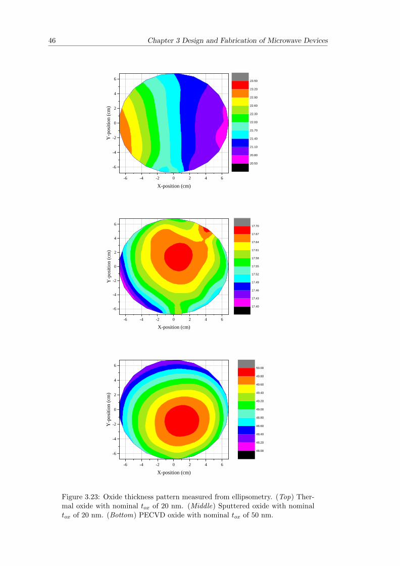
46 Chapter 3 Design and Fabrication of Microwave Devices
- 6 - 4 - 2 0 2 4 6
- 6
- 4
- 2
0
2
4
6
Y-pos
ition (
cm)
X - p o s i t i o n ( c m )
2 0 . 5 0
2 0 . 8 0
2 1 . 1 0
2 1 . 4 0
2 1 . 7 0
2 2 . 0 0
2 2 . 3 0
2 2 . 6 0
2 2 . 9 0
2 3 . 2 0
2 3 . 5 0
- 6 - 4 - 2 0 2 4 6- 6
- 4
- 2
0
2
4
6
Y-pos
ition (
cm)
X - p o s i t i o n ( c m )
1 7 . 4 0
1 7 . 4 3
1 7 . 4 6
1 7 . 4 9
1 7 . 5 2
1 7 . 5 5
1 7 . 5 8
1 7 . 6 1
1 7 . 6 4
1 7 . 6 7
1 7 . 7 0
- 6 - 4 - 2 0 2 4 6
- 6
- 4
- 2
0
2
4
6
Y-pos
ition (
cm)
X - p o s i t i o n ( c m )
4 8 . 0 0
4 8 . 2 0
4 8 . 4 0
4 8 . 6 0
4 8 . 8 0
4 9 . 0 0
4 9 . 2 0
4 9 . 4 0
4 9 . 6 0
4 9 . 8 0
5 0 . 0 0
Figure 3.23: Oxide thickness pattern measured from ellipsometry. (Top) Ther-mal oxide with nominal tox of 20 nm. (Middle) Sputtered oxide with nominaltox of 20 nm. (Bottom) PECVD oxide with nominal tox of 50 nm.
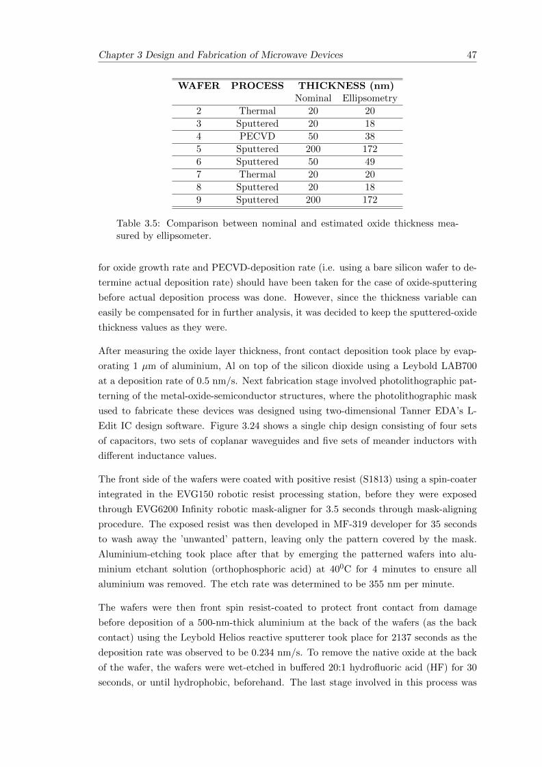
Chapter 3 Design and Fabrication of Microwave Devices 47
WAFER PROCESS THICKNESS (nm)Nominal Ellipsometry
2 Thermal 20 20
3 Sputtered 20 18
4 PECVD 50 38
5 Sputtered 200 172
6 Sputtered 50 49
7 Thermal 20 20
8 Sputtered 20 18
9 Sputtered 200 172
Table 3.5: Comparison between nominal and estimated oxide thickness mea-sured by ellipsometer.
for oxide growth rate and PECVD-deposition rate (i.e. using a bare silicon wafer to de-
termine actual deposition rate) should have been taken for the case of oxide-sputtering
before actual deposition process was done. However, since the thickness variable can
easily be compensated for in further analysis, it was decided to keep the sputtered-oxide
thickness values as they were.
After measuring the oxide layer thickness, front contact deposition took place by evap-
orating 1 µm of aluminium, Al on top of the silicon dioxide using a Leybold LAB700
at a deposition rate of 0.5 nm/s. Next fabrication stage involved photolithographic pat-
terning of the metal-oxide-semiconductor structures, where the photolithographic mask
used to fabricate these devices was designed using two-dimensional Tanner EDA’s L-
Edit IC design software. Figure 3.24 shows a single chip design consisting of four sets
of capacitors, two sets of coplanar waveguides and five sets of meander inductors with
different inductance values.
The front side of the wafers were coated with positive resist (S1813) using a spin-coater
integrated in the EVG150 robotic resist processing station, before they were exposed
through EVG6200 Infinity robotic mask-aligner for 3.5 seconds through mask-aligning
procedure. The exposed resist was then developed in MF-319 developer for 35 seconds
to wash away the ’unwanted’ pattern, leaving only the pattern covered by the mask.
Aluminium-etching took place after that by emerging the patterned wafers into alu-
minium etchant solution (orthophosphoric acid) at 400C for 4 minutes to ensure all
aluminium was removed. The etch rate was determined to be 355 nm per minute.
The wafers were then front spin resist-coated to protect front contact from damage
before deposition of a 500-nm-thick aluminium at the back of the wafers (as the back
contact) using the Leybold Helios reactive sputterer took place for 2137 seconds as the
deposition rate was observed to be 0.234 nm/s. To remove the native oxide at the back
of the wafer, the wafers were wet-etched in buffered 20:1 hydrofluoric acid (HF) for 30
seconds, or until hydrophobic, beforehand. The last stage involved in this process was
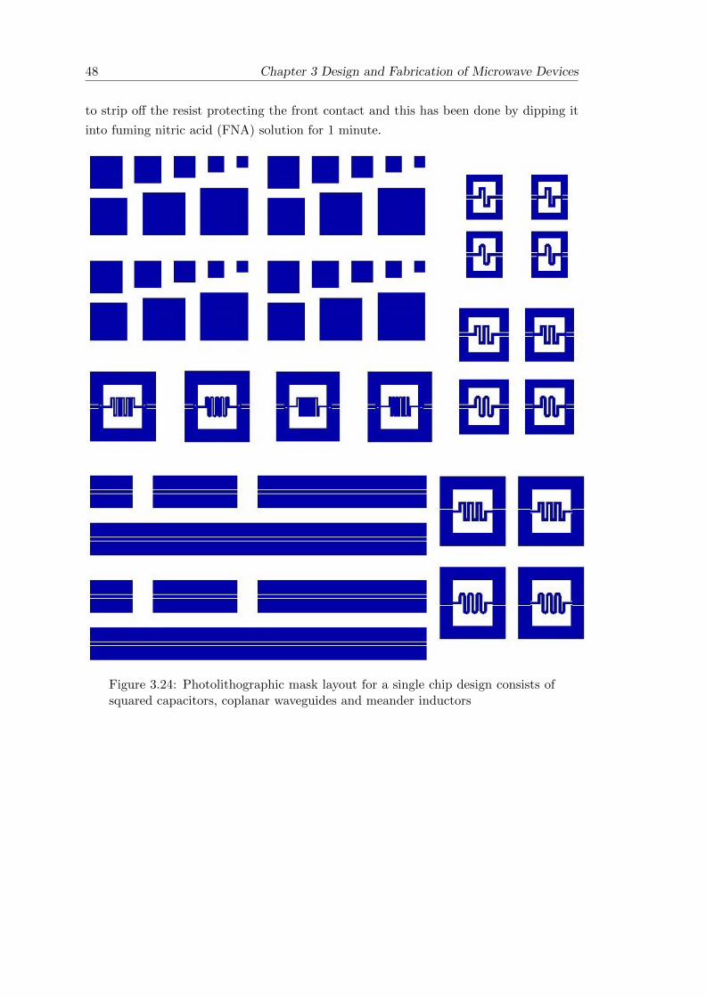
48 Chapter 3 Design and Fabrication of Microwave Devices
to strip off the resist protecting the front contact and this has been done by dipping it
into fuming nitric acid (FNA) solution for 1 minute.
Figure 3.24: Photolithographic mask layout for a single chip design consists ofsquared capacitors, coplanar waveguides and meander inductors
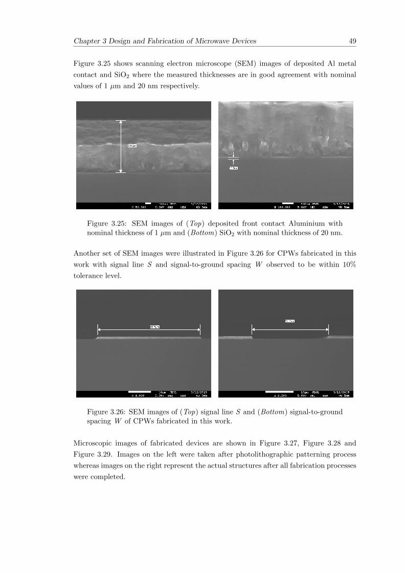
Chapter 3 Design and Fabrication of Microwave Devices 49
Figure 3.25 shows scanning electron microscope (SEM) images of deposited Al metal
contact and SiO2 where the measured thicknesses are in good agreement with nominal
values of 1 µm and 20 nm respectively.
Figure 3.25: SEM images of (Top) deposited front contact Aluminium withnominal thickness of 1 µm and (Bottom) SiO2 with nominal thickness of 20 nm.
Another set of SEM images were illustrated in Figure 3.26 for CPWs fabricated in this
work with signal line S and signal-to-ground spacing W observed to be within 10%
tolerance level.
Figure 3.26: SEM images of (Top) signal line S and (Bottom) signal-to-groundspacing W of CPWs fabricated in this work.
Microscopic images of fabricated devices are shown in Figure 3.27, Figure 3.28 and
Figure 3.29. Images on the left were taken after photolithographic patterning process
whereas images on the right represent the actual structures after all fabrication processes
were completed.
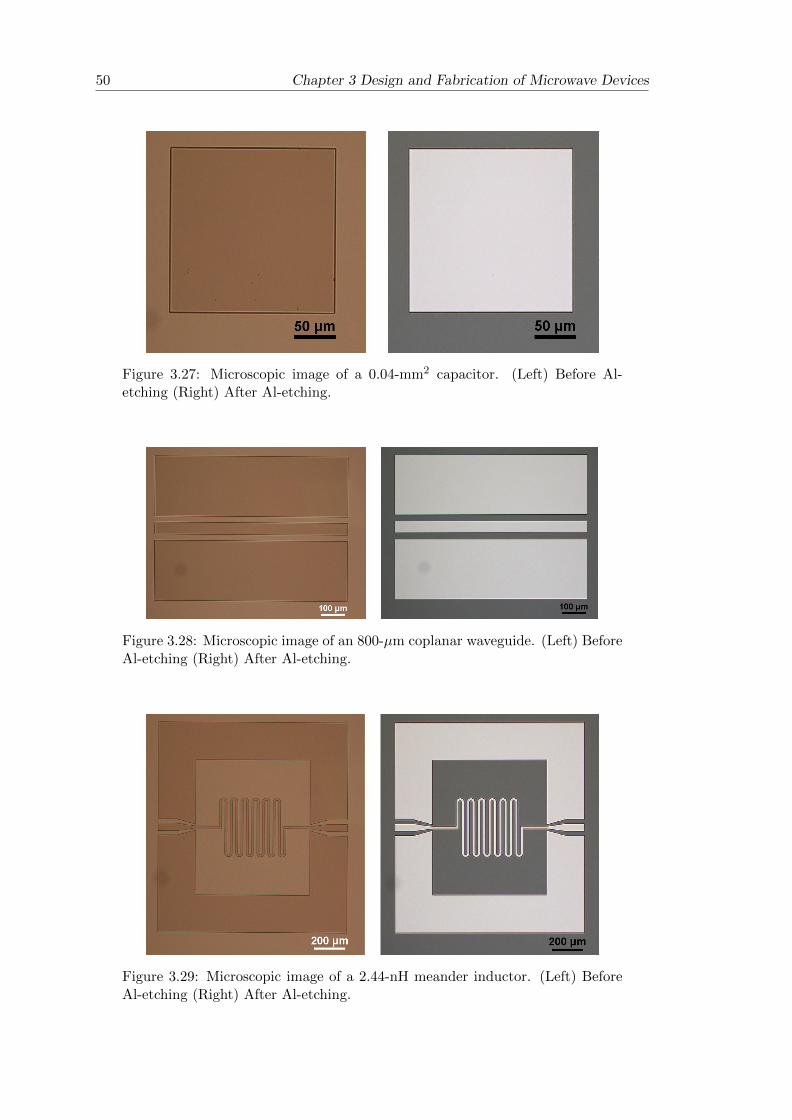
50 Chapter 3 Design and Fabrication of Microwave Devices
Figure 3.27: Microscopic image of a 0.04-mm2 capacitor. (Left) Before Al-etching (Right) After Al-etching.
Figure 3.28: Microscopic image of an 800-µm coplanar waveguide. (Left) BeforeAl-etching (Right) After Al-etching.
Figure 3.29: Microscopic image of a 2.44-nH meander inductor. (Left) BeforeAl-etching (Right) After Al-etching.
Chapter 3 Design and Fabrication of Microwave Devices 51
3.5 Summary
Planar capacitors, coplanar waveguides and meander inductors were designed. Backside
metallisation was considered in the design where the designed structures were optimised
to provide a sufficient platform for the study of PSC suppression on Au-compensated HR-
Si substrates. All design were realised onto photolithographic mask before fabrication
of devices took place.

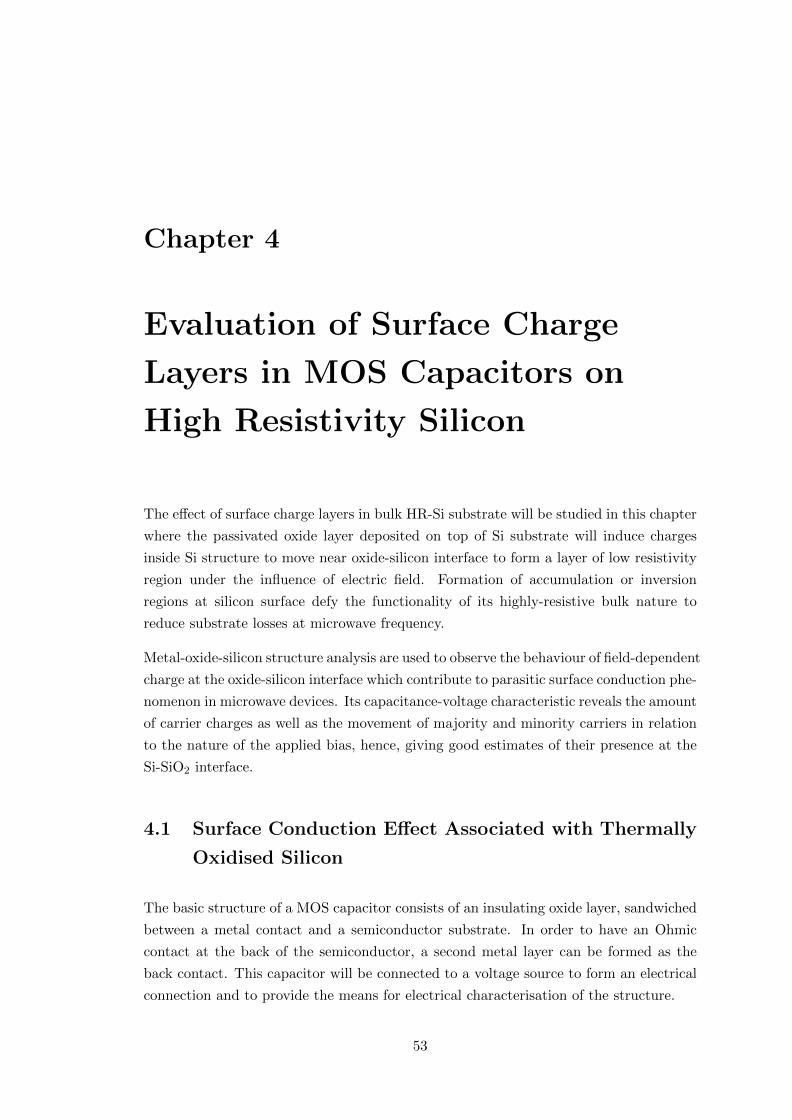
Chapter 4
Evaluation of Surface Charge
Layers in MOS Capacitors on
High Resistivity Silicon
The effect of surface charge layers in bulk HR-Si substrate will be studied in this chapter
where the passivated oxide layer deposited on top of Si substrate will induce charges
inside Si structure to move near oxide-silicon interface to form a layer of low resistivity
region under the influence of electric field. Formation of accumulation or inversion
regions at silicon surface defy the functionality of its highly-resistive bulk nature to
reduce substrate losses at microwave frequency.
Metal-oxide-silicon structure analysis are used to observe the behaviour of field-dependent
charge at the oxide-silicon interface which contribute to parasitic surface conduction phe-
nomenon in microwave devices. Its capacitance-voltage characteristic reveals the amount
of carrier charges as well as the movement of majority and minority carriers in relation
to the nature of the applied bias, hence, giving good estimates of their presence at the
Si-SiO2 interface.
4.1 Surface Conduction Effect Associated with Thermally
Oxidised Silicon
The basic structure of a MOS capacitor consists of an insulating oxide layer, sandwiched
between a metal contact and a semiconductor substrate. In order to have an Ohmic
contact at the back of the semiconductor, a second metal layer can be formed as the
back contact. This capacitor will be connected to a voltage source to form an electrical
connection and to provide the means for electrical characterisation of the structure.
53
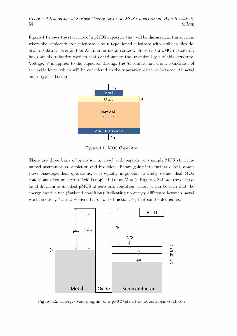
54Chapter 4 Evaluation of Surface Charge Layers in MOS Capacitors on High Resistivity
Silicon
Figure 4.1 shows the structure of a pMOS capacitor that will be discussed in this section,
where the semiconductor substrate is an n-type doped substrate with a silicon dioxide,
SiO2 insulating layer and an Aluminium metal contact. Since it is a pMOS capacitor,
holes are the minority carriers that contribute to the inversion layer of this structure.
Voltage, V is applied to the capacitor through the Al contact and d is the thickness of
the oxide layer, which will be considered as the separation distance between Al metal
and n-type substrate.
Figure 4.1: MOS Capacitor
There are three basis of operation involved with regards to a simple MOS structure
named accumulation, depletion and inversion. Before going into further details about
these bias-dependent operations, it is equally important to firstly define ideal MOS
conditions when no electric field is applied, i.e. at V = 0. Figure 4.2 shows the energy-
band diagram of an ideal pMOS at zero bias condition, where it can be seen that the
energy band is flat (flatband condition), indicating no energy difference between metal
work function, Φm and semiconductor work function, Φs that can be defined as:
Figure 4.2: Energy-band diagram of a pMOS structure at zero bias condition
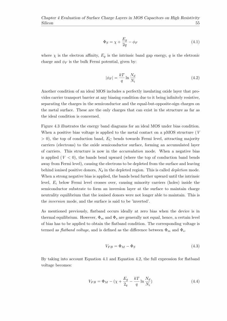
Chapter 4 Evaluation of Surface Charge Layers in MOS Capacitors on High ResistivitySilicon 55
ΦS = χ+Eg2q− φF (4.1)
where χ is the electron affinity, Eg is the intrinsic band gap energy, q is the eletronic
charge and φF is the bulk Fermi potential, given by:
|φF | =kT
qlnNd
Ni(4.2)
Another condition of an ideal MOS includes a perfectly insulating oxide layer that pro-
vides carrier transport barrier at any biasing condition due to it being infinitely resistive,
separating the charges in the semiconductor and the equal-but-opposite-sign charges on
the metal surface. These are the only charges that can exist in the structure as far as
the ideal condition is concerned.
Figure 4.3 illustrates the energy band diagrams for an ideal MOS under bias condition.
When a positive bias voltage is applied to the metal contact on a pMOS structure (V
> 0), the top of conduction band, EC bends towards Fermi level, attracting majority
carriers (electrons) to the oxide semiconductor surface, forming an accumulated layer
of carriers. This structure is now in the accumulation mode. When a negative bias
is applied (V < 0), the bands bend upward (where the top of conduction band bends
away from Fermi level), causing the electrons to be depleted from the surface and leaving
behind ionised positive donors, Nd in the depleted region. This is called depletion mode.
When a strong negative bias is applied, the bands bend further upward until the intrinsic
level, Ei below Fermi level crosses over, causing minority carriers (holes) inside the
semiconductor substrate to form an inversion layer at the surface to maintain charge
neutrality equilibrium that the ionised donors were not longer able to maintain. This is
the inversion mode, and the surface is said to be ’inverted’.
As mentioned previously, flatband occurs ideally at zero bias when the device is in
thermal equilibrium. However, Φm and Φs are generally not equal, hence, a certain level
of bias has to be applied to obtain the flatband condition. The corresponding voltage is
termed as flatband voltage, and is defined as the difference between Φm and Φs.
VFB = ΦM − ΦS (4.3)
By taking into account Equation 4.1 and Equation 4.2, the full expression for flatband
voltage becomes:
VFB = ΦM − (χ+Eg2q− kT
qlnNd
Ni) (4.4)
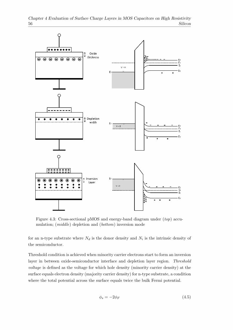
56Chapter 4 Evaluation of Surface Charge Layers in MOS Capacitors on High Resistivity
Silicon
Figure 4.3: Cross-sectional pMOS and energy-band diagram under (top) accu-mulation; (middle) depletion and (bottom) inversion mode
for an n-type substrate where Nd is the donor density and Ni is the intrinsic density of
the semiconductor.
Threshold condition is achieved when minority carrier electrons start to form an inversion
layer in between oxide-semiconductor interface and depletion layer region. Threshold
voltage is defined as the voltage for which hole density (minority carrier density) at the
surface equals electron density (majority carrier density) for n-type substrate, a condition
where the total potential across the surface equals twice the bulk Fermi potential.
φs = −2φF (4.5)
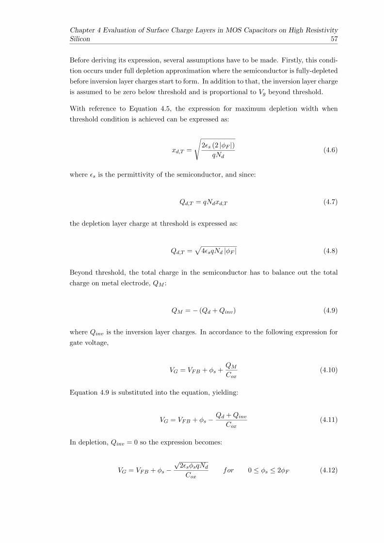
Chapter 4 Evaluation of Surface Charge Layers in MOS Capacitors on High ResistivitySilicon 57
Before deriving its expression, several assumptions have to be made. Firstly, this condi-
tion occurs under full depletion approximation where the semiconductor is fully-depleted
before inversion layer charges start to form. In addition to that, the inversion layer charge
is assumed to be zero below threshold and is proportional to Vg beyond threshold.
With reference to Equation 4.5, the expression for maximum depletion width when
threshold condition is achieved can be expressed as:
xd,T =
√2εs (2 |φF |)
qNd(4.6)
where εs is the permittivity of the semiconductor, and since:
Qd,T = qNdxd,T (4.7)
the depletion layer charge at threshold is expressed as:
Qd,T =√
4εsqNd |φF | (4.8)
Beyond threshold, the total charge in the semiconductor has to balance out the total
charge on metal electrode, QM :
QM = − (Qd +Qinv) (4.9)
where Qinv is the inversion layer charges. In accordance to the following expression for
gate voltage,
VG = VFB + φs +QMCox
(4.10)
Equation 4.9 is substituted into the equation, yielding:
VG = VFB + φs −Qd +Qinv
Cox(4.11)
In depletion, Qinv = 0 so the expression becomes:
VG = VFB + φs −√
2εsφsqNd
Coxfor 0 ≤ φs ≤ 2φF (4.12)
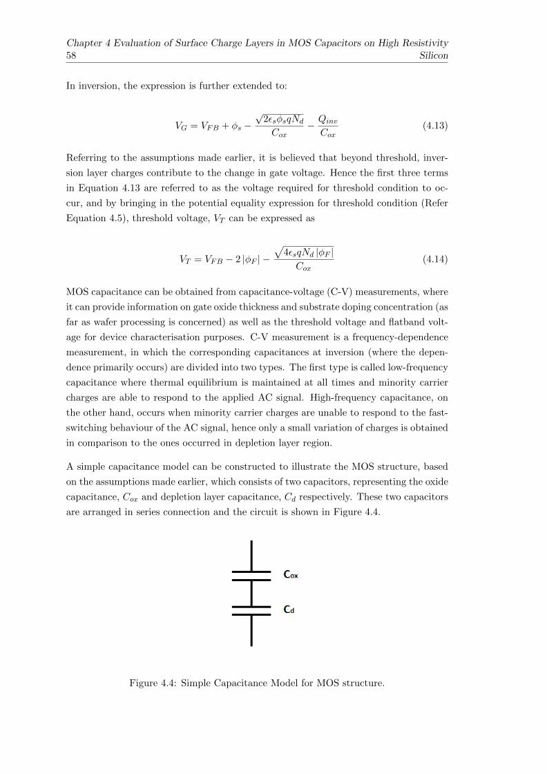
58Chapter 4 Evaluation of Surface Charge Layers in MOS Capacitors on High Resistivity
Silicon
In inversion, the expression is further extended to:
VG = VFB + φs −√
2εsφsqNd
Cox− Qinv
Cox(4.13)
Referring to the assumptions made earlier, it is believed that beyond threshold, inver-
sion layer charges contribute to the change in gate voltage. Hence the first three terms
in Equation 4.13 are referred to as the voltage required for threshold condition to oc-
cur, and by bringing in the potential equality expression for threshold condition (Refer
Equation 4.5), threshold voltage, VT can be expressed as
VT = VFB − 2 |φF | −√
4εsqNd |φF |Cox
(4.14)
MOS capacitance can be obtained from capacitance-voltage (C-V) measurements, where
it can provide information on gate oxide thickness and substrate doping concentration (as
far as wafer processing is concerned) as well as the threshold voltage and flatband volt-
age for device characterisation purposes. C-V measurement is a frequency-dependence
measurement, in which the corresponding capacitances at inversion (where the depen-
dence primarily occurs) are divided into two types. The first type is called low-frequency
capacitance where thermal equilibrium is maintained at all times and minority carrier
charges are able to respond to the applied AC signal. High-frequency capacitance, on
the other hand, occurs when minority carrier charges are unable to respond to the fast-
switching behaviour of the AC signal, hence only a small variation of charges is obtained
in comparison to the ones occurred in depletion layer region.
A simple capacitance model can be constructed to illustrate the MOS structure, based
on the assumptions made earlier, which consists of two capacitors, representing the oxide
capacitance, Cox and depletion layer capacitance, Cd respectively. These two capacitors
are arranged in series connection and the circuit is shown in Figure 4.4.
Figure 4.4: Simple Capacitance Model for MOS structure.
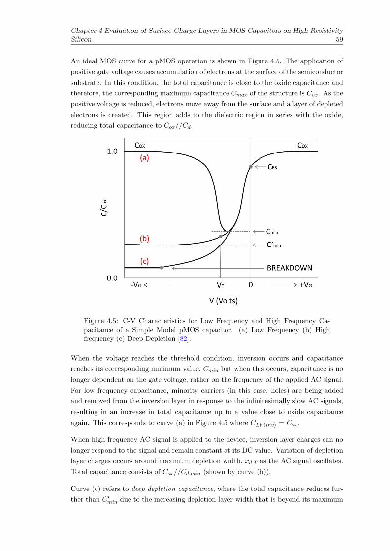
Chapter 4 Evaluation of Surface Charge Layers in MOS Capacitors on High ResistivitySilicon 59
An ideal MOS curve for a pMOS operation is shown in Figure 4.5. The application of
positive gate voltage causes accumulation of electrons at the surface of the semiconductor
substrate. In this condition, the total capacitance is close to the oxide capacitance and
therefore, the corresponding maximum capacitance Cmax of the structure is Cox. As the
positive voltage is reduced, electrons move away from the surface and a layer of depleted
electrons is created. This region adds to the dielectric region in series with the oxide,
reducing total capacitance to Cox//Cd.
Figure 4.5: C-V Characteristics for Low Frequency and High Frequency Ca-pacitance of a Simple Model pMOS capacitor. (a) Low Frequency (b) Highfrequency (c) Deep Depletion [82].
When the voltage reaches the threshold condition, inversion occurs and capacitance
reaches its corresponding minimum value, Cmin but when this occurs, capacitance is no
longer dependent on the gate voltage, rather on the frequency of the applied AC signal.
For low frequency capacitance, minority carriers (in this case, holes) are being added
and removed from the inversion layer in response to the infinitesimally slow AC signals,
resulting in an increase in total capacitance up to a value close to oxide capacitance
again. This corresponds to curve (a) in Figure 4.5 where CLF (inv) = Cox.
When high frequency AC signal is applied to the device, inversion layer charges can no
longer respond to the signal and remain constant at its DC value. Variation of depletion
layer charges occurs around maximum depletion width, xd,T as the AC signal oscillates.
Total capacitance consists of Cox//Cd,min (shown by curve (b)).
Curve (c) refers to deep depletion capacitance, where the total capacitance reduces fur-
ther than C ′min due to the increasing depletion layer width that is beyond its maximum
60Chapter 4 Evaluation of Surface Charge Layers in MOS Capacitors on High Resistivity
Silicon
value as the voltage reduces. This phenomena occurs as holes are not generated fast
enough to keep up to the fast-changing AC signal to form an inversion layer hence, caus-
ing the depleted region to be extended further. In this case, total capacitance would
be very much less than C ′min until it reaches a breakdown. To reduce this effect and
allow full inversion, capacitance-voltage measurement needs to be done by sweeping the
DC voltage from inversion to accumulation, and light needs to be present before the
measurement takes place.
The ideal MOS structure discussed earlier assumes a perfectly insulating layer in between
metal contact and semiconductor substrate that is infinitely resistive. Unfortunately,
this is not the case in reality since oxidation of silicon introduces defects in the Si-SiO2
interface, where electrically-conducting and non-conducting charges exist. The associ-
ated charges affect MOS performance in such a way that an inversion or accumulation
layer can form at zero or low bias thus, creating a layer of low resistivity region at the
interface and altering bias-dependent capacitance characteristics. This causes unreliable
wafer-processing and device performance. Figure 4.6 illustrates four types of charges
associated with oxidised silicon.
Figure 4.6: Associated Charges at Si-SiO2 interface [82].
Interface trapped charge, Dit exists at the interface, within the forbidden gap due to
structural defects, metal impurities and other radiation-caused effects. Unlike oxide
charges, this type of charge can be electrically active i.e. becomes positive donor trap
by giving up an electron or negative acceptor trap by accepting an electron. Hence,
it can be neutralised by low temperature annealing under hydrogen environment at
450 C. It affects MOS capacitance is such a way that there is a change of charges
when the interface-trap level crosses the Fermi level with the application of electric field,
altering the MOS characteristic by stretching out the curve obtained from low frequency
capacitance-voltage measurement.
Meanwhile, fixed oxide charge, Qf is usually caused by structural defects in silicon during
the oxidation process and is located within 2.5 nm of the silicon-silicon dioxide interface
[83]. Its density depends on oxidation ambient and temperature, cooling condition and
silicon orientation, and is very little affected by the oxide thickness and doping type or
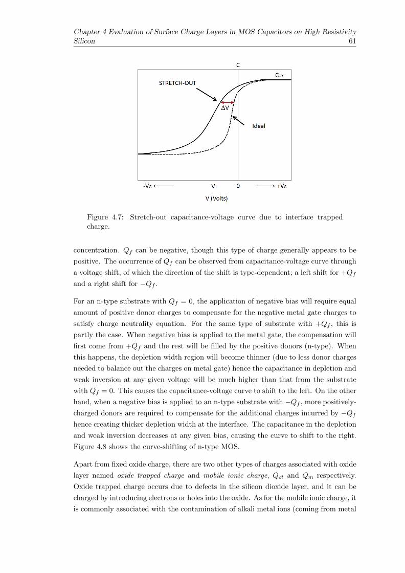
Chapter 4 Evaluation of Surface Charge Layers in MOS Capacitors on High ResistivitySilicon 61
Figure 4.7: Stretch-out capacitance-voltage curve due to interface trappedcharge.
concentration. Qf can be negative, though this type of charge generally appears to be
positive. The occurrence of Qf can be observed from capacitance-voltage curve through
a voltage shift, of which the direction of the shift is type-dependent; a left shift for +Qf
and a right shift for −Qf .
For an n-type substrate with Qf = 0, the application of negative bias will require equal
amount of positive donor charges to compensate for the negative metal gate charges to
satisfy charge neutrality equation. For the same type of substrate with +Qf , this is
partly the case. When negative bias is applied to the metal gate, the compensation will
first come from +Qf and the rest will be filled by the positive donors (n-type). When
this happens, the depletion width region will become thinner (due to less donor charges
needed to balance out the charges on metal gate) hence the capacitance in depletion and
weak inversion at any given voltage will be much higher than that from the substrate
with Qf = 0. This causes the capacitance-voltage curve to shift to the left. On the other
hand, when a negative bias is applied to an n-type substrate with −Qf , more positively-
charged donors are required to compensate for the additional charges incurred by −Qfhence creating thicker depletion width at the interface. The capacitance in the depletion
and weak inversion decreases at any given bias, causing the curve to shift to the right.
Figure 4.8 shows the curve-shifting of n-type MOS.
Apart from fixed oxide charge, there are two other types of charges associated with oxide
layer named oxide trapped charge and mobile ionic charge, Qot and Qm respectively.
Oxide trapped charge occurs due to defects in the silicon dioxide layer, and it can be
charged by introducing electrons or holes into the oxide. As for the mobile ionic charge, it
is commonly associated with the contamination of alkali metal ions (coming from metal
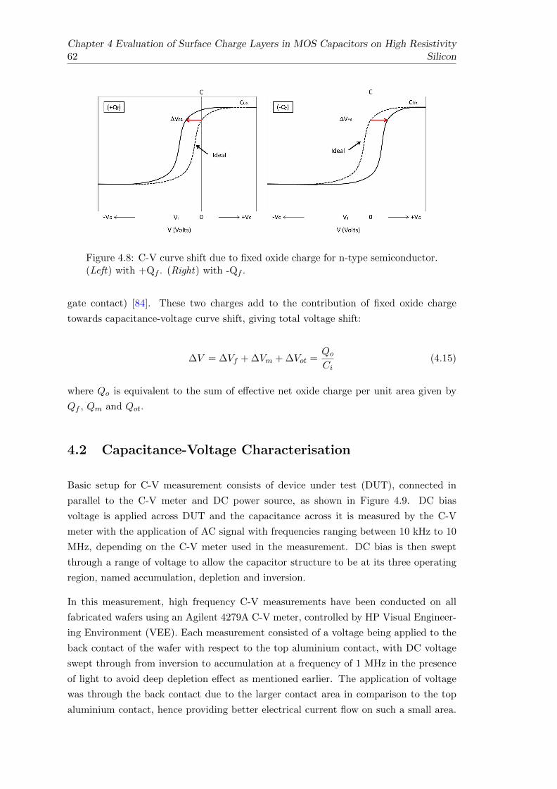
62Chapter 4 Evaluation of Surface Charge Layers in MOS Capacitors on High Resistivity
Silicon
Figure 4.8: C-V curve shift due to fixed oxide charge for n-type semiconductor.(Left) with +Qf . (Right) with -Qf .
gate contact) [84]. These two charges add to the contribution of fixed oxide charge
towards capacitance-voltage curve shift, giving total voltage shift:
∆V = ∆Vf + ∆Vm + ∆Vot =QoCi
(4.15)
where Qo is equivalent to the sum of effective net oxide charge per unit area given by
Qf , Qm and Qot.
4.2 Capacitance-Voltage Characterisation
Basic setup for C-V measurement consists of device under test (DUT), connected in
parallel to the C-V meter and DC power source, as shown in Figure 4.9. DC bias
voltage is applied across DUT and the capacitance across it is measured by the C-V
meter with the application of AC signal with frequencies ranging between 10 kHz to 10
MHz, depending on the C-V meter used in the measurement. DC bias is then swept
through a range of voltage to allow the capacitor structure to be at its three operating
region, named accumulation, depletion and inversion.
In this measurement, high frequency C-V measurements have been conducted on all
fabricated wafers using an Agilent 4279A C-V meter, controlled by HP Visual Engineer-
ing Environment (VEE). Each measurement consisted of a voltage being applied to the
back contact of the wafer with respect to the top aluminium contact, with DC voltage
swept through from inversion to accumulation at a frequency of 1 MHz in the presence
of light to avoid deep depletion effect as mentioned earlier. The application of voltage
was through the back contact due to the larger contact area in comparison to the top
aluminium contact, hence providing better electrical current flow on such a small area.
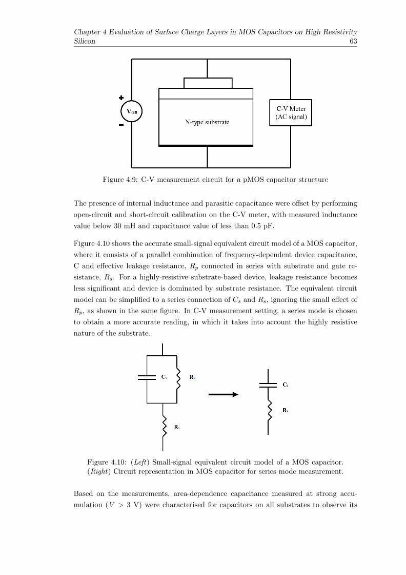
Chapter 4 Evaluation of Surface Charge Layers in MOS Capacitors on High ResistivitySilicon 63
Figure 4.9: C-V measurement circuit for a pMOS capacitor structure
The presence of internal inductance and parasitic capacitance were offset by performing
open-circuit and short-circuit calibration on the C-V meter, with measured inductance
value below 30 mH and capacitance value of less than 0.5 pF.
Figure 4.10 shows the accurate small-signal equivalent circuit model of a MOS capacitor,
where it consists of a parallel combination of frequency-dependent device capacitance,
C and effective leakage resistance, Rp connected in series with substrate and gate re-
sistance, Rs. For a highly-resistive substrate-based device, leakage resistance becomes
less significant and device is dominated by substrate resistance. The equivalent circuit
model can be simplified to a series connection of Cs and Rs, ignoring the small effect of
Rp, as shown in the same figure. In C-V measurement setting, a series mode is chosen
to obtain a more accurate reading, in which it takes into account the highly resistive
nature of the substrate.
Figure 4.10: (Left) Small-signal equivalent circuit model of a MOS capacitor.(Right) Circuit representation in MOS capacitor for series mode measurement.
Based on the measurements, area-dependence capacitance measured at strong accu-
mulation (V > 3 V) were characterised for capacitors on all substrates to observe its
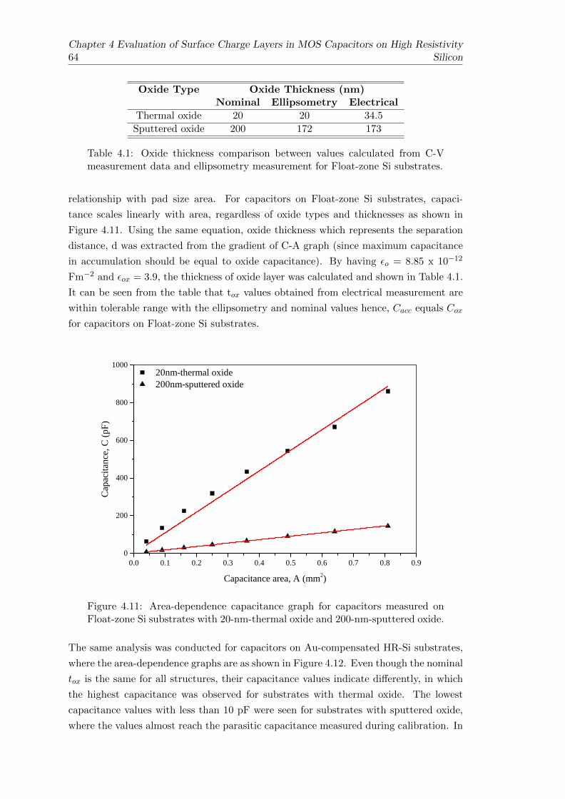
64Chapter 4 Evaluation of Surface Charge Layers in MOS Capacitors on High Resistivity
Silicon
Oxide Type Oxide Thickness (nm)Nominal Ellipsometry Electrical
Thermal oxide 20 20 34.5
Sputtered oxide 200 172 173
Table 4.1: Oxide thickness comparison between values calculated from C-Vmeasurement data and ellipsometry measurement for Float-zone Si substrates.
relationship with pad size area. For capacitors on Float-zone Si substrates, capaci-
tance scales linearly with area, regardless of oxide types and thicknesses as shown in
Figure 4.11. Using the same equation, oxide thickness which represents the separation
distance, d was extracted from the gradient of C-A graph (since maximum capacitance
in accumulation should be equal to oxide capacitance). By having εo = 8.85 x 10⁻¹²
Fm−2 and εox = 3.9, the thickness of oxide layer was calculated and shown in Table 4.1.
It can be seen from the table that tox values obtained from electrical measurement are
within tolerable range with the ellipsometry and nominal values hence, Cacc equals Cox
for capacitors on Float-zone Si substrates.
0 . 0 0 . 1 0 . 2 0 . 3 0 . 4 0 . 5 0 . 6 0 . 7 0 . 8 0 . 90
2 0 0
4 0 0
6 0 0
8 0 0
1 0 0 0 2 0 n m - t h e r m a l o x i d e 2 0 0 n m - s p u t t e r e d o x i d e
Capac
itance,
C (pF
)
C a p a c i t a n c e a r e a , A ( m m 2 )
Figure 4.11: Area-dependence capacitance graph for capacitors measured onFloat-zone Si substrates with 20-nm-thermal oxide and 200-nm-sputtered oxide.
The same analysis was conducted for capacitors on Au-compensated HR-Si substrates,
where the area-dependence graphs are as shown in Figure 4.12. Even though the nominal
tox is the same for all structures, their capacitance values indicate differently, in which
the highest capacitance was observed for substrates with thermal oxide. The lowest
capacitance values with less than 10 pF were seen for substrates with sputtered oxide,
where the values almost reach the parasitic capacitance measured during calibration. In
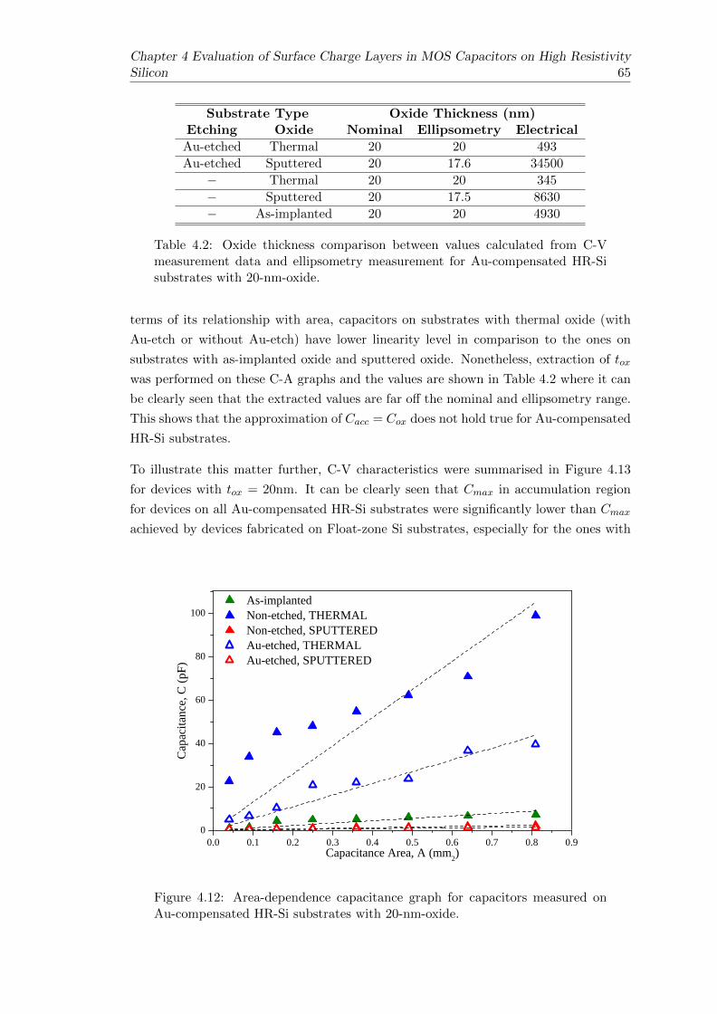
Chapter 4 Evaluation of Surface Charge Layers in MOS Capacitors on High ResistivitySilicon 65
Substrate Type Oxide Thickness (nm)Etching Oxide Nominal Ellipsometry Electrical
Au-etched Thermal 20 20 493
Au-etched Sputtered 20 17.6 34500
− Thermal 20 20 345
− Sputtered 20 17.5 8630
− As-implanted 20 20 4930
Table 4.2: Oxide thickness comparison between values calculated from C-Vmeasurement data and ellipsometry measurement for Au-compensated HR-Sisubstrates with 20-nm-oxide.
terms of its relationship with area, capacitors on substrates with thermal oxide (with
Au-etch or without Au-etch) have lower linearity level in comparison to the ones on
substrates with as-implanted oxide and sputtered oxide. Nonetheless, extraction of tox
was performed on these C-A graphs and the values are shown in Table 4.2 where it can
be clearly seen that the extracted values are far off the nominal and ellipsometry range.
This shows that the approximation of Cacc = Cox does not hold true for Au-compensated
HR-Si substrates.
To illustrate this matter further, C-V characteristics were summarised in Figure 4.13
for devices with tox = 20nm. It can be clearly seen that Cmax in accumulation region
for devices on all Au-compensated HR-Si substrates were significantly lower than Cmax
achieved by devices fabricated on Float-zone Si substrates, especially for the ones with
0 . 0 0 . 1 0 . 2 0 . 3 0 . 4 0 . 5 0 . 6 0 . 7 0 . 8 0 . 90
2 0
4 0
6 0
8 0
1 0 0 A s - i m p l a n t e d N o n - e t c h e d , T H E R M A L N o n - e t c h e d , S P U T T E R E D A u - e t c h e d , T H E R M A L A u - e t c h e d , S P U T T E R E D
Capac
itance,
C (pF
)
C a p a c i t a n c e A r e a , A ( m m 2 )
Figure 4.12: Area-dependence capacitance graph for capacitors measured onAu-compensated HR-Si substrates with 20-nm-oxide.
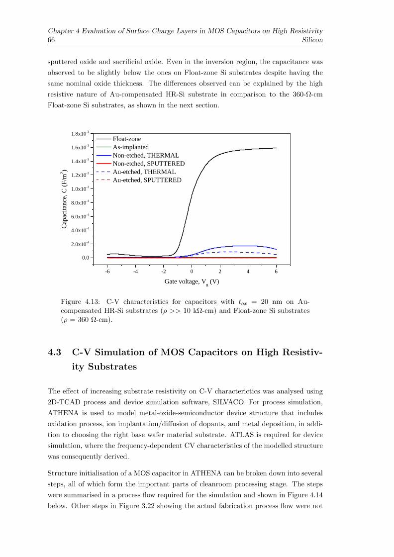
66Chapter 4 Evaluation of Surface Charge Layers in MOS Capacitors on High Resistivity
Silicon
sputtered oxide and sacrificial oxide. Even in the inversion region, the capacitance was
observed to be slightly below the ones on Float-zone Si substrates despite having the
same nominal oxide thickness. The differences observed can be explained by the high
resistive nature of Au-compensated HR-Si substrate in comparison to the 360-Ω-cm
Float-zone Si substrates, as shown in the next section.
- 6 - 4 - 2 0 2 4 60 . 0
2 . 0 x 1 0 - 4
4 . 0 x 1 0 - 4
6 . 0 x 1 0 - 4
8 . 0 x 1 0 - 4
1 . 0 x 1 0 - 3
1 . 2 x 1 0 - 3
1 . 4 x 1 0 - 3
1 . 6 x 1 0 - 3
1 . 8 x 1 0 - 3 F l o a t - z o n e A s - i m p l a n t e d N o n - e t c h e d , T H E R M A L N o n - e t c h e d , S P U T T E R E D A u - e t c h e d , T H E R M A L A u - e t c h e d , S P U T T E R E D
Capac
itance,
C (F/
m2 )
G a t e v o l t a g e , V g ( V )
Figure 4.13: C-V characteristics for capacitors with tox = 20 nm on Au-compensated HR-Si substrates (ρ >> 10 kΩ-cm) and Float-zone Si substrates(ρ = 360 Ω-cm).
4.3 C-V Simulation of MOS Capacitors on High Resistiv-
ity Substrates
The effect of increasing substrate resistivity on C-V characterictics was analysed using
2D-TCAD process and device simulation software, SILVACO. For process simulation,
ATHENA is used to model metal-oxide-semiconductor device structure that includes
oxidation process, ion implantation/diffusion of dopants, and metal deposition, in addi-
tion to choosing the right base wafer material substrate. ATLAS is required for device
simulation, where the frequency-dependent CV characteristics of the modelled structure
was consequently derived.
Structure initialisation of a MOS capacitor in ATHENA can be broken down into several
steps, all of which form the important parts of cleanroom processing stage. The steps
were summarised in a process flow required for the simulation and shown in Figure 4.14
below. Other steps in Figure 3.22 showing the actual fabrication process flow were not
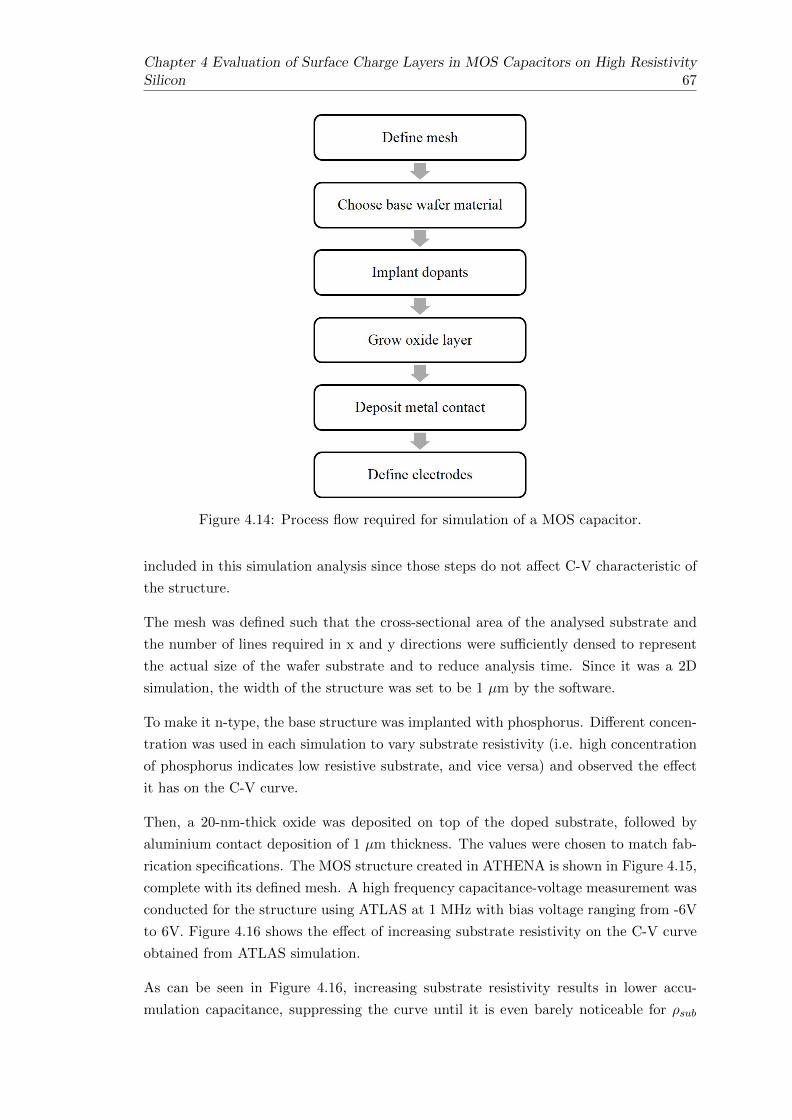
Chapter 4 Evaluation of Surface Charge Layers in MOS Capacitors on High ResistivitySilicon 67
Figure 4.14: Process flow required for simulation of a MOS capacitor.
included in this simulation analysis since those steps do not affect C-V characteristic of
the structure.
The mesh was defined such that the cross-sectional area of the analysed substrate and
the number of lines required in x and y directions were sufficiently densed to represent
the actual size of the wafer substrate and to reduce analysis time. Since it was a 2D
simulation, the width of the structure was set to be 1 µm by the software.
To make it n-type, the base structure was implanted with phosphorus. Different concen-
tration was used in each simulation to vary substrate resistivity (i.e. high concentration
of phosphorus indicates low resistive substrate, and vice versa) and observed the effect
it has on the C-V curve.
Then, a 20-nm-thick oxide was deposited on top of the doped substrate, followed by
aluminium contact deposition of 1 µm thickness. The values were chosen to match fab-
rication specifications. The MOS structure created in ATHENA is shown in Figure 4.15,
complete with its defined mesh. A high frequency capacitance-voltage measurement was
conducted for the structure using ATLAS at 1 MHz with bias voltage ranging from -6V
to 6V. Figure 4.16 shows the effect of increasing substrate resistivity on the C-V curve
obtained from ATLAS simulation.
As can be seen in Figure 4.16, increasing substrate resistivity results in lower accu-
mulation capacitance, suppressing the curve until it is even barely noticeable for ρsub
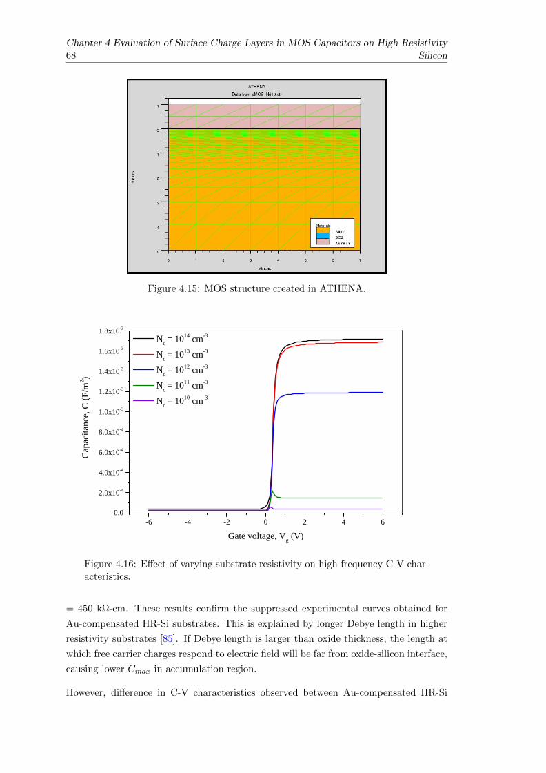
68Chapter 4 Evaluation of Surface Charge Layers in MOS Capacitors on High Resistivity
Silicon
Figure 4.15: MOS structure created in ATHENA.
- 6 - 4 - 2 0 2 4 60 . 0
2 . 0 x 1 0 - 4
4 . 0 x 1 0 - 4
6 . 0 x 1 0 - 4
8 . 0 x 1 0 - 4
1 . 0 x 1 0 - 3
1 . 2 x 1 0 - 3
1 . 4 x 1 0 - 3
1 . 6 x 1 0 - 3
1 . 8 x 1 0 - 3
N d = 1 0 1 4 c m - 3
N d = 1 0 1 3 c m - 3
N d = 1 0 1 2 c m - 3
N d = 1 0 1 1 c m - 3
N d = 1 0 1 0 c m - 3
Capac
itance,
C (F/
m2 )
G a t e v o l t a g e , V g ( V )
Figure 4.16: Effect of varying substrate resistivity on high frequency C-V char-acteristics.
= 450 kΩ-cm. These results confirm the suppressed experimental curves obtained for
Au-compensated HR-Si substrates. This is explained by longer Debye length in higher
resistivity substrates [85]. If Debye length is larger than oxide thickness, the length at
which free carrier charges respond to electric field will be far from oxide-silicon interface,
causing lower Cmax in accumulation region.
However, difference in C-V characteristics observed between Au-compensated HR-Si
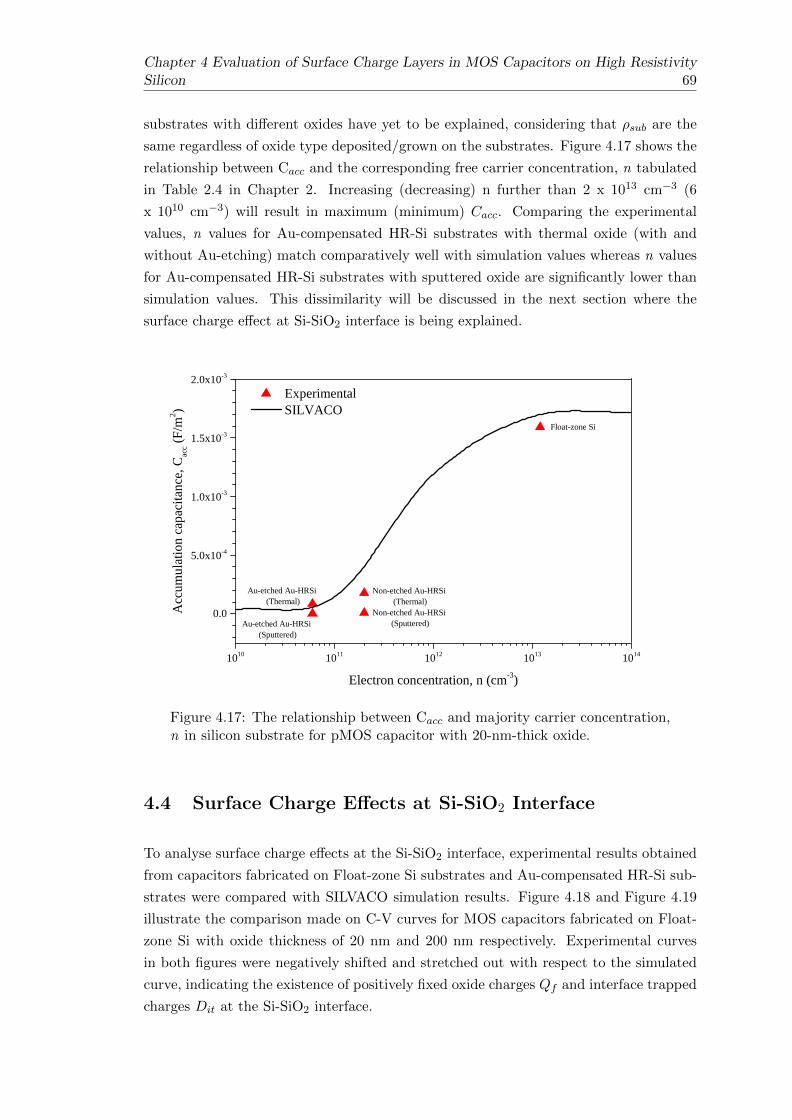
Chapter 4 Evaluation of Surface Charge Layers in MOS Capacitors on High ResistivitySilicon 69
substrates with different oxides have yet to be explained, considering that ρsub are the
same regardless of oxide type deposited/grown on the substrates. Figure 4.17 shows the
relationship between Cacc and the corresponding free carrier concentration, n tabulated
in Table 2.4 in Chapter 2. Increasing (decreasing) n further than 2 x 1013 cm−3 (6
x 1010 cm−3) will result in maximum (minimum) Cacc. Comparing the experimental
values, n values for Au-compensated HR-Si substrates with thermal oxide (with and
without Au-etching) match comparatively well with simulation values whereas n values
for Au-compensated HR-Si substrates with sputtered oxide are significantly lower than
simulation values. This dissimilarity will be discussed in the next section where the
surface charge effect at Si-SiO2 interface is being explained.
1 0 1 0 1 0 1 1 1 0 1 2 1 0 1 3 1 0 1 4
0 . 0
5 . 0 x 1 0 - 4
1 . 0 x 1 0 - 3
1 . 5 x 1 0 - 3
2 . 0 x 1 0 - 3
N o n - e t c h e d A u - H R S i ( S p u t t e r e d )A u - e t c h e d A u - H R S i
( S p u t t e r e d )
A u - e t c h e d A u - H R S i ( T h e r m a l )Ac
cumula
tion c
apacita
nce, C
acc (F
/m2 )
E l e c t r o n c o n c e n t r a t i o n , n ( c m - 3 )
E x p e r i m e n t a l S I L V A C O
N o n - e t c h e d A u - H R S i ( T h e r m a l )
F l o a t - z o n e S i
Figure 4.17: The relationship between Cacc and majority carrier concentration,n in silicon substrate for pMOS capacitor with 20-nm-thick oxide.
4.4 Surface Charge Effects at Si-SiO2 Interface
To analyse surface charge effects at the Si-SiO2 interface, experimental results obtained
from capacitors fabricated on Float-zone Si substrates and Au-compensated HR-Si sub-
strates were compared with SILVACO simulation results. Figure 4.18 and Figure 4.19
illustrate the comparison made on C-V curves for MOS capacitors fabricated on Float-
zone Si with oxide thickness of 20 nm and 200 nm respectively. Experimental curves
in both figures were negatively shifted and stretched out with respect to the simulated
curve, indicating the existence of positively fixed oxide charges Qf and interface trapped
charges Dit at the Si-SiO2 interface.
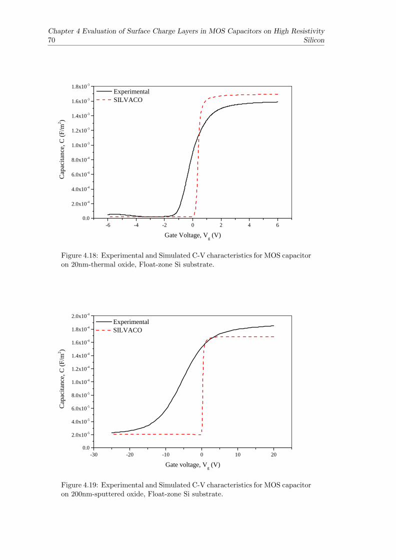
70Chapter 4 Evaluation of Surface Charge Layers in MOS Capacitors on High Resistivity
Silicon
- 6 - 4 - 2 0 2 4 60 . 0
2 . 0 x 1 0 - 4
4 . 0 x 1 0 - 4
6 . 0 x 1 0 - 4
8 . 0 x 1 0 - 4
1 . 0 x 1 0 - 3
1 . 2 x 1 0 - 3
1 . 4 x 1 0 - 3
1 . 6 x 1 0 - 3
1 . 8 x 1 0 - 3 E x p e r i m e n t a l S I L V A C O
Capac
itance,
C (F/
m2 )
G a t e V o l t a g e , V g ( V )
Figure 4.18: Experimental and Simulated C-V characteristics for MOS capacitoron 20nm-thermal oxide, Float-zone Si substrate.
- 3 0 - 2 0 - 1 0 0 1 0 2 00 . 0
2 . 0 x 1 0 - 5
4 . 0 x 1 0 - 5
6 . 0 x 1 0 - 5
8 . 0 x 1 0 - 5
1 . 0 x 1 0 - 4
1 . 2 x 1 0 - 4
1 . 4 x 1 0 - 4
1 . 6 x 1 0 - 4
1 . 8 x 1 0 - 4
2 . 0 x 1 0 - 4
E x p e r i m e n t a l S I L V A C O
Capac
itance,
C (F/
m2 )
G a t e v o l t a g e , V g ( V )
Figure 4.19: Experimental and Simulated C-V characteristics for MOS capacitoron 200nm-sputtered oxide, Float-zone Si substrate.
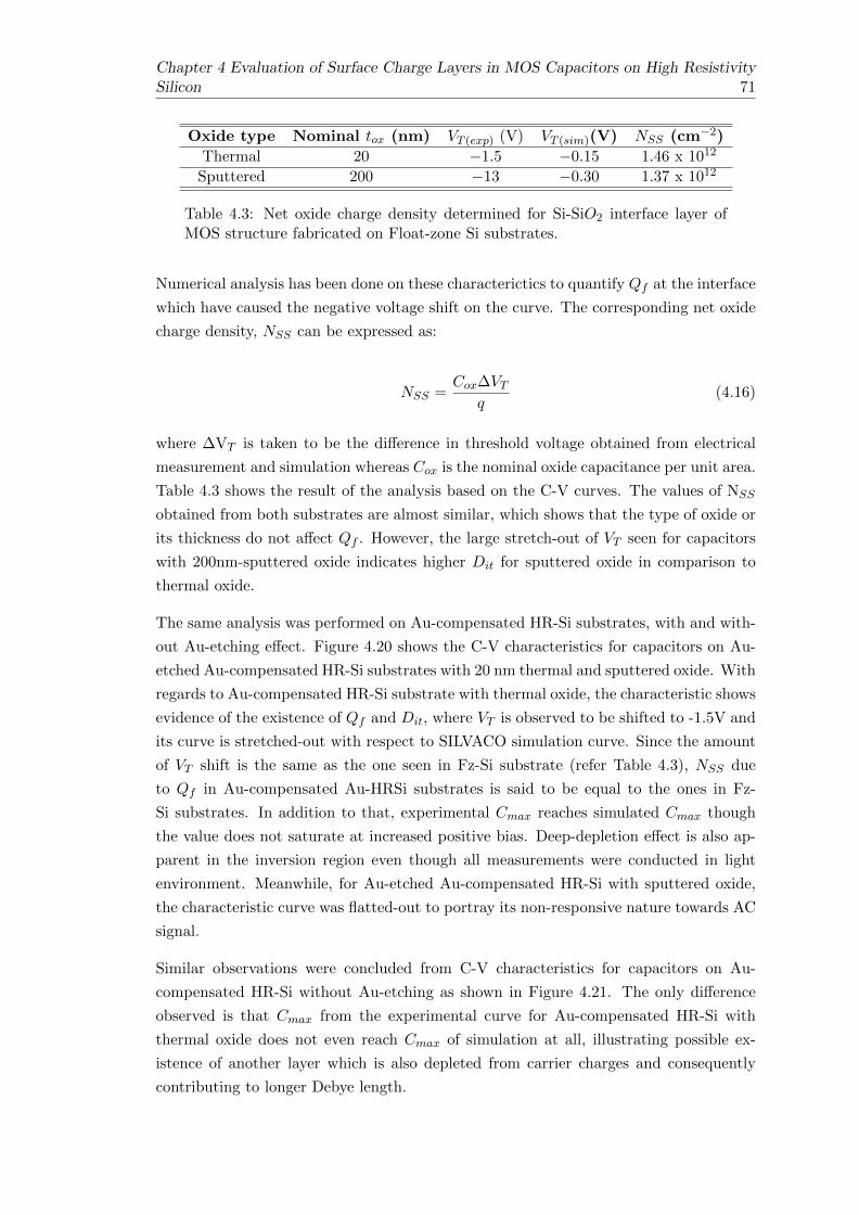
Chapter 4 Evaluation of Surface Charge Layers in MOS Capacitors on High ResistivitySilicon 71
Oxide type Nominal tox (nm) VT (exp) (V) VT (sim)(V) NSS (cm−2)
Thermal 20 −1.5 −0.15 1.46 x 10¹²
Sputtered 200 −13 −0.30 1.37 x 10¹²
Table 4.3: Net oxide charge density determined for Si-SiO2 interface layer ofMOS structure fabricated on Float-zone Si substrates.
Numerical analysis has been done on these characterictics to quantify Qf at the interface
which have caused the negative voltage shift on the curve. The corresponding net oxide
charge density, NSS can be expressed as:
NSS =Cox∆VT
q(4.16)
where ∆VT is taken to be the difference in threshold voltage obtained from electrical
measurement and simulation whereas Cox is the nominal oxide capacitance per unit area.
Table 4.3 shows the result of the analysis based on the C-V curves. The values of NSS
obtained from both substrates are almost similar, which shows that the type of oxide or
its thickness do not affect Qf . However, the large stretch-out of VT seen for capacitors
with 200nm-sputtered oxide indicates higher Dit for sputtered oxide in comparison to
thermal oxide.
The same analysis was performed on Au-compensated HR-Si substrates, with and with-
out Au-etching effect. Figure 4.20 shows the C-V characteristics for capacitors on Au-
etched Au-compensated HR-Si substrates with 20 nm thermal and sputtered oxide. With
regards to Au-compensated HR-Si substrate with thermal oxide, the characteristic shows
evidence of the existence of Qf and Dit, where VT is observed to be shifted to -1.5V and
its curve is stretched-out with respect to SILVACO simulation curve. Since the amount
of VT shift is the same as the one seen in Fz-Si substrate (refer Table 4.3), NSS due
to Qf in Au-compensated Au-HRSi substrates is said to be equal to the ones in Fz-
Si substrates. In addition to that, experimental Cmax reaches simulated Cmax though
the value does not saturate at increased positive bias. Deep-depletion effect is also ap-
parent in the inversion region even though all measurements were conducted in light
environment. Meanwhile, for Au-etched Au-compensated HR-Si with sputtered oxide,
the characteristic curve was flatted-out to portray its non-responsive nature towards AC
signal.
Similar observations were concluded from C-V characteristics for capacitors on Au-
compensated HR-Si without Au-etching as shown in Figure 4.21. The only difference
observed is that Cmax from the experimental curve for Au-compensated HR-Si with
thermal oxide does not even reach Cmax of simulation at all, illustrating possible ex-
istence of another layer which is also depleted from carrier charges and consequently
contributing to longer Debye length.
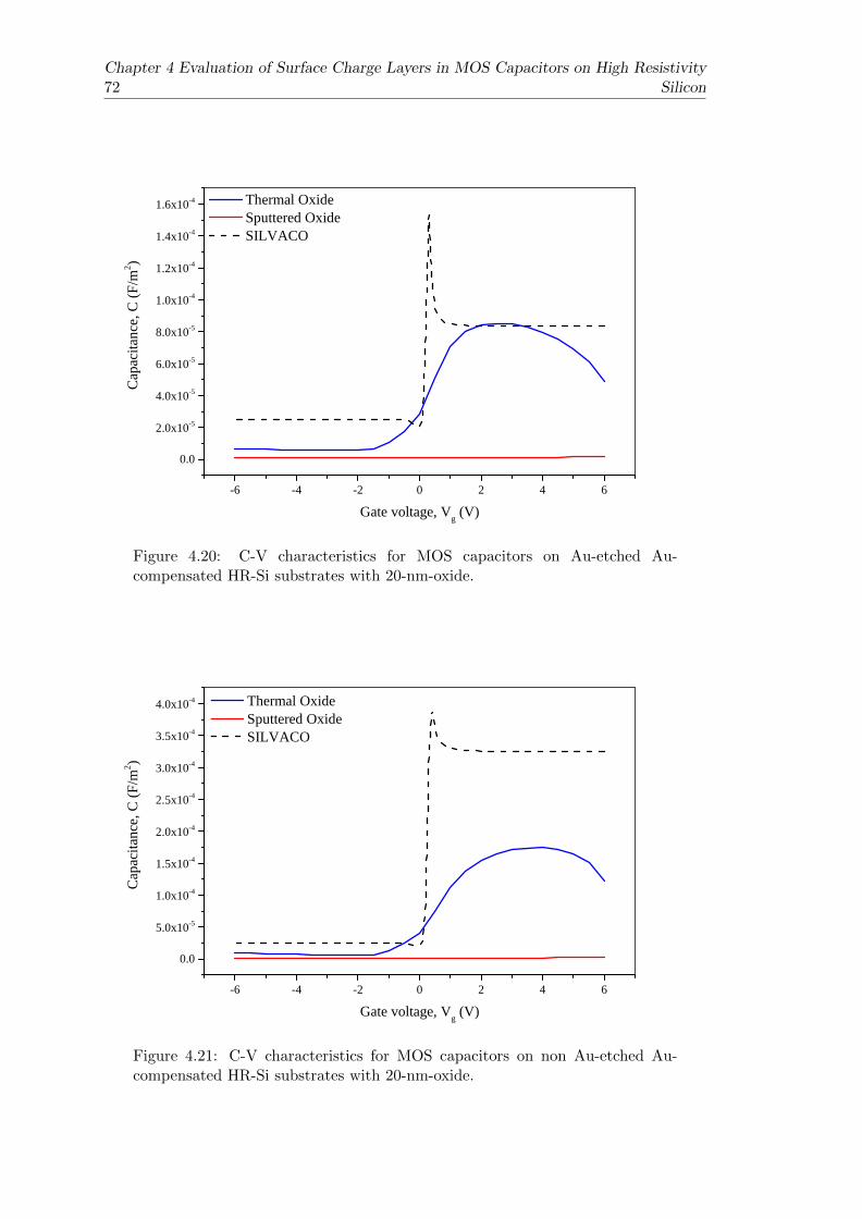
72Chapter 4 Evaluation of Surface Charge Layers in MOS Capacitors on High Resistivity
Silicon
- 6 - 4 - 2 0 2 4 6
0 . 0
2 . 0 x 1 0 - 5
4 . 0 x 1 0 - 5
6 . 0 x 1 0 - 5
8 . 0 x 1 0 - 5
1 . 0 x 1 0 - 4
1 . 2 x 1 0 - 4
1 . 4 x 1 0 - 4
1 . 6 x 1 0 - 4 T h e r m a l O x i d e S p u t t e r e d O x i d e S I L V A C O
Capac
itance,
C (F/
m2 )
G a t e v o l t a g e , V g ( V )
Figure 4.20: C-V characteristics for MOS capacitors on Au-etched Au-compensated HR-Si substrates with 20-nm-oxide.
- 6 - 4 - 2 0 2 4 6
0 . 0
5 . 0 x 1 0 - 5
1 . 0 x 1 0 - 4
1 . 5 x 1 0 - 4
2 . 0 x 1 0 - 4
2 . 5 x 1 0 - 4
3 . 0 x 1 0 - 4
3 . 5 x 1 0 - 4
4 . 0 x 1 0 - 4 T h e r m a l O x i d e S p u t t e r e d O x i d e S I L V A C O
Capac
itance,
C (F/
m2 )
G a t e v o l t a g e , V g ( V )
Figure 4.21: C-V characteristics for MOS capacitors on non Au-etched Au-compensated HR-Si substrates with 20-nm-oxide.
Chapter 4 Evaluation of Surface Charge Layers in MOS Capacitors on High ResistivitySilicon 73
4.5 Summary
Capacitance-voltage characteristics of Au-compensated HR-Si substrates were studied
in this chapter, where the approximation of Cacc = Cox is shown to be invalid due to the
high resistivity nature of the substrates and longer Debye length. SILVACO simulations
were conducted to show the effect of high resistivity substrates on C-V characterisations.
Suppression of accumulation response is seen for high resistivity substrates especially
when the value starts to reach 45 kΩ-cm, confirming the experimental C-V suppression
shown by Au-compensated HR-Si substrates. Analysis on surface charge effect on Au-
compensated HR-Si substrates shows potential suppression for substrates with sputtered
oxide where non-responsive C-V curves were obtained at range of voltage measured.

Chapter 5
Suppression of Parasitic Surface
Conduction using CPW Loss
Analysis
As has been discussed in the previous chapter, capacitance-voltage characteristics for
MOS structure fabricated on Au-compensated Si substrates show reduced dependency
on bias voltage, indicating the possibility of PSC suppression at Au-compensated Si
substrate surfaces. In this chapter, microwave characteristics of coplanar waveguides are
used to evaluate the potential of Au-compensated Si substrates to suppress PSC effect
and increase substrate resistivity effectively to ensure low-loss microwave performance
is achieved.
For the purpose of this work, conductor-backed coplanar waveguides were designed and
fabricated on top of Au-compensated Si substrate where particular attention has been
paid on the planar dimension of the CPW structure to minimise losses contributed
by impedance-mismatching. The losses measured are hence, mostly coming from the
substrates. Microwave measurements were conducted to analyse attenuation loss of
coplanar waveguides and to evaluate factors affecting loss characteristics of these devices
on Au-compensated Si substrate.
5.1 Attenuation Loss Mechanism of a Coplanar Waveguide
Coplanar waveguide transmission lines are used to transmit microwave frequency sig-
nals in MMICs technology. Unlike microstrip lines, coplanar waveguides offer reduced
complexity in terms of fabrication and circuit integration due to the ground lines being
on the same plane as its signal line. In addition, its planar dimension can be designed
75
76 Chapter 5 Suppression of Parasitic Surface Conduction using CPW Loss Analysis
in such a way to fit any required characteristic impedance hence the risk of impedance-
mismatching between source and load can be reduced.
Schematic structure of a conventional CPW on a naked substrate without top cover is
shown in Figure 5.1 where the ground lines, G have the same planarity as the signal
line denoted by S. Travelling wave propagates in the outward direction from signal line
to ground lines through the air and into the substrate, as shown in Figure 5.2.
Figure 5.1: Conventional CPW on a naked substrate without top cover [86].
Figure 5.2: Electric field distributions for CPW in even mode [86].
Full signal transmission is not achievable in any transmission line structure including
CPW. Therefore, losses are introduced. Apart from radiation losses, there are two main
mechanisms of CPW losses; ohmic and dielectric, which represent losses associated with
CPW metal conductor lines and substrate’s finite resistance, respectively [86]. The
expression for conductor loss in CPWs (in dB/length) is given by:
αc =8.68RS
√εr,eff
240πK(k)K(k′)(1− k2)[Φ(S) + Φ(W )] (5.1)
Chapter 5 Suppression of Parasitic Surface Conduction using CPW Loss Analysis 77
where:
Φ(x) =1
x
[π + ln
(4πx
t
1− k1 + k
)](5.2)
k =S
S + 2W(5.3)
k′
=√
1− k2 (5.4)
and K(k) is the complete elliptic integral of the first kind and εr,eff is the effective
permittivity of the structure. RS is metal surface resistance represented by:
RS =√πfρµo (5.5)
where f is the operating frequency, ρ is metal resistivity and µo is vacuum permeability
given by 4πx10−7 H/m. Based on the relationships seen in Equation 5.2 to Equation 5.5,
αc shows strong dependency on CPW dimension and metal resistivity and is shown to
be directly proportional to√f .
Meanwhile, substrate loss, αd contributed by substrate’s finite resistance is given by [86]
(in dB/length):
αd = 27.3εr√εr,eff
εr,eff − 1
εr − 1
tanδ
λo(5.6)
where λo is wavelength of free-space and tan δ is dielectric loss tangent of the semicon-
ductor expressed by [87]:
tanδ = tanδd +σ
ωεoεr(5.7)
As can be seen in Equation 5.7, there are two parts of losses in semiconductor. tan
δd represents intrinsic loss coming from pure semiconductor whereas the latter part of
the equation is contributed extrinsically by doping property of semiconductor, mainly
originating from free charge carriers. For doped semiconductor substrate operating
in high frequency range, tan δd is considered to be small and can be neglected [88].
Assuming a thick substrate (h → ∞), Equation 5.6 can be simplified to give [89]:
αd = 8.6830π
√εr,effρSi
(5.8)
78 Chapter 5 Suppression of Parasitic Surface Conduction using CPW Loss Analysis
where ρsub is substrate resistivity. From the expression, substrate loss is seen to be
inversely proportional to ρsub indicating the importance of having substrate with high
resistivity to reduce total CPW losses.
Apart from the losses coming from αc and αd, there is another contribution that makes
up the total CPW losses in silicon-based MMICs (SiMMICs) circuit application and
that is called bias-dependent interface loss as discussed in [31]. Interface losses in CPW
occur as a result of PSC effect where the movement of charge carriers at the interface
due to change in electric field creates a low resistivity region at the silicon surface with
the magnitude of loss generated depends greatly on bias voltage. This loss can only be
analysed qualitatively from microwave characterisation where the total attenuation loss
of a CPW is obtained [32,90,91].
For a two-port S-parameter measurement, the expression for CPW attenuation can be
derived from Beer-Lambert law [92]:
IlIo
= 10−αl (5.9)
where Il is the intensity of transmitted power through CPW line with length l and Io is
the intensity of incident power. It can be further expanded to give:
IlIo
=Il
I −R=
Il/I
1−R/I= 10−αl (5.10)
with I total power supplied by VNA and R is the reflected power. The numerator of the
third expression represents the fraction of transmitted power through the system from
port 1 to port 2 whereas the denominator represents the fraction of reflected power back
to port 1 with respect to total power generated. The fractional terms can be translated
into magnitude of S21, in the former case and S11 for the latter, giving |S12|2 and |S11|2
respectively.
Hence, the expression can be re-written as:
[|S21|2
1− |S11|2
]= 10−αl (5.11)
As a result, total attenuation loss of a CPW in dB per unit l can be expressed as:
α = −10
llog10
[|S21|2
1− |S11|2
](5.12)
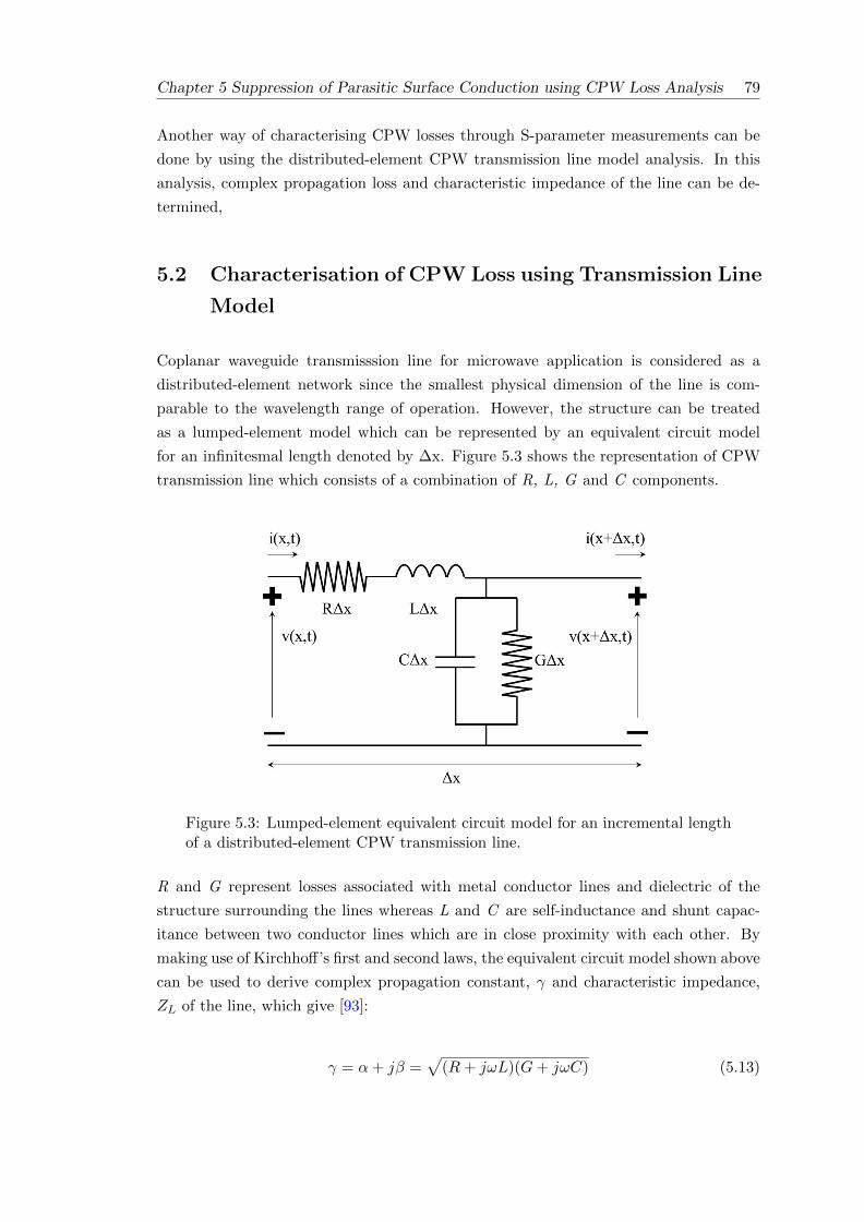
Chapter 5 Suppression of Parasitic Surface Conduction using CPW Loss Analysis 79
Another way of characterising CPW losses through S-parameter measurements can be
done by using the distributed-element CPW transmission line model analysis. In this
analysis, complex propagation loss and characteristic impedance of the line can be de-
termined,
5.2 Characterisation of CPW Loss using Transmission Line
Model
Coplanar waveguide transmisssion line for microwave application is considered as a
distributed-element network since the smallest physical dimension of the line is com-
parable to the wavelength range of operation. However, the structure can be treated
as a lumped-element model which can be represented by an equivalent circuit model
for an infinitesmal length denoted by ∆x. Figure 5.3 shows the representation of CPW
transmission line which consists of a combination of R, L, G and C components.
Figure 5.3: Lumped-element equivalent circuit model for an incremental lengthof a distributed-element CPW transmission line.
R and G represent losses associated with metal conductor lines and dielectric of the
structure surrounding the lines whereas L and C are self-inductance and shunt capac-
itance between two conductor lines which are in close proximity with each other. By
making use of Kirchhoff’s first and second laws, the equivalent circuit model shown above
can be used to derive complex propagation constant, γ and characteristic impedance,
ZL of the line, which give [93]:
γ = α+ jβ =√
(R+ jωL)(G+ jωC) (5.13)
80 Chapter 5 Suppression of Parasitic Surface Conduction using CPW Loss Analysis
ZL =
√R+ jωL
G+ jωC(5.14)
where α and β are attenuation constant and phase constant respectively.
Rearranging equations Equation 5.13 and Equation 5.14 will then provide R, L, G and
C expressions in terms of γ and ZL as depicted below:
R = Re(γ · ZL) (5.15)
L =Im(γ · ZL)
ω(5.16)
G = Re(γ
ZL) (5.17)
C =Im( γ
ZL)
ω(5.18)
where ω is the angular frequency given by 2πf.
Extraction of γ and ZL can be obtained from on-wafer microwave characterisation,
where two-port, frequency-dependent S-parameter are measured by a vector network
analyser (VNA). Under perfectly-matched transmission line condition, power transfer
ratio is equal to 1 where there is no reflection of transmission signal at both ports and
transmitted power at one port is reciprocal to one another [94]. This means that losses
are attributed purely from metal and dielectric of the structure to give:
S11 = S22 (5.19)
S21 = S12 (5.20)
By taking into account power losses due to reflected signal at both ports individually
(represented by reflection coefficient Γ) and by considering Zo = 50 Ω as VNA’s reference
impedance, γ and ZL expressions in terms of S-parameter values can be found from [95]:
e−γL =
(1− S2
11 + S221
2S21±
√(S2
11 − S212 + 1)2 − (2S2
11)
(2S21)2
)−1(5.21)
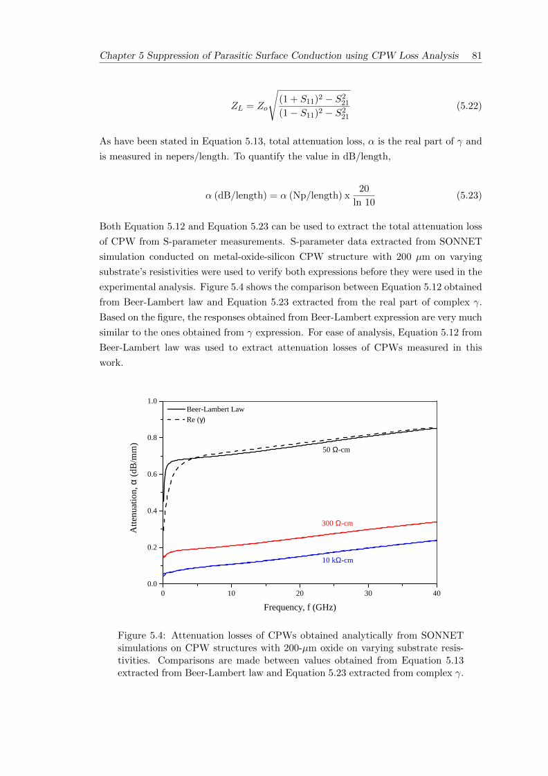
Chapter 5 Suppression of Parasitic Surface Conduction using CPW Loss Analysis 81
ZL = Zo
√(1 + S11)2 − S2
21
(1− S11)2 − S221
(5.22)
As have been stated in Equation 5.13, total attenuation loss, α is the real part of γ and
is measured in nepers/length. To quantify the value in dB/length,
α (dB/length) = α (Np/length) x20
ln 10(5.23)
Both Equation 5.12 and Equation 5.23 can be used to extract the total attenuation loss
of CPW from S-parameter measurements. S-parameter data extracted from SONNET
simulation conducted on metal-oxide-silicon CPW structure with 200 µm on varying
substrate’s resistivities were used to verify both expressions before they were used in the
experimental analysis. Figure 5.4 shows the comparison between Equation 5.12 obtained
from Beer-Lambert law and Equation 5.23 extracted from the real part of complex γ.
Based on the figure, the responses obtained from Beer-Lambert expression are very much
similar to the ones obtained from γ expression. For ease of analysis, Equation 5.12 from
Beer-Lambert law was used to extract attenuation losses of CPWs measured in this
work.
0 1 0 2 0 3 0 4 00 . 0
0 . 2
0 . 4
0 . 6
0 . 8
1 . 0
1 0 k Ω - c m
3 0 0 Ω - c m
B e e r - L a m b e r t L a w R e ( γ )
Attenu
ation, α
(dB/m
m)
F r e q u e n c y , f ( G H z )
5 0 Ω - c m
Figure 5.4: Attenuation losses of CPWs obtained analytically from SONNETsimulations on CPW structures with 200-µm oxide on varying substrate resis-tivities. Comparisons are made between values obtained from Equation 5.13extracted from Beer-Lambert law and Equation 5.23 extracted from complex γ.
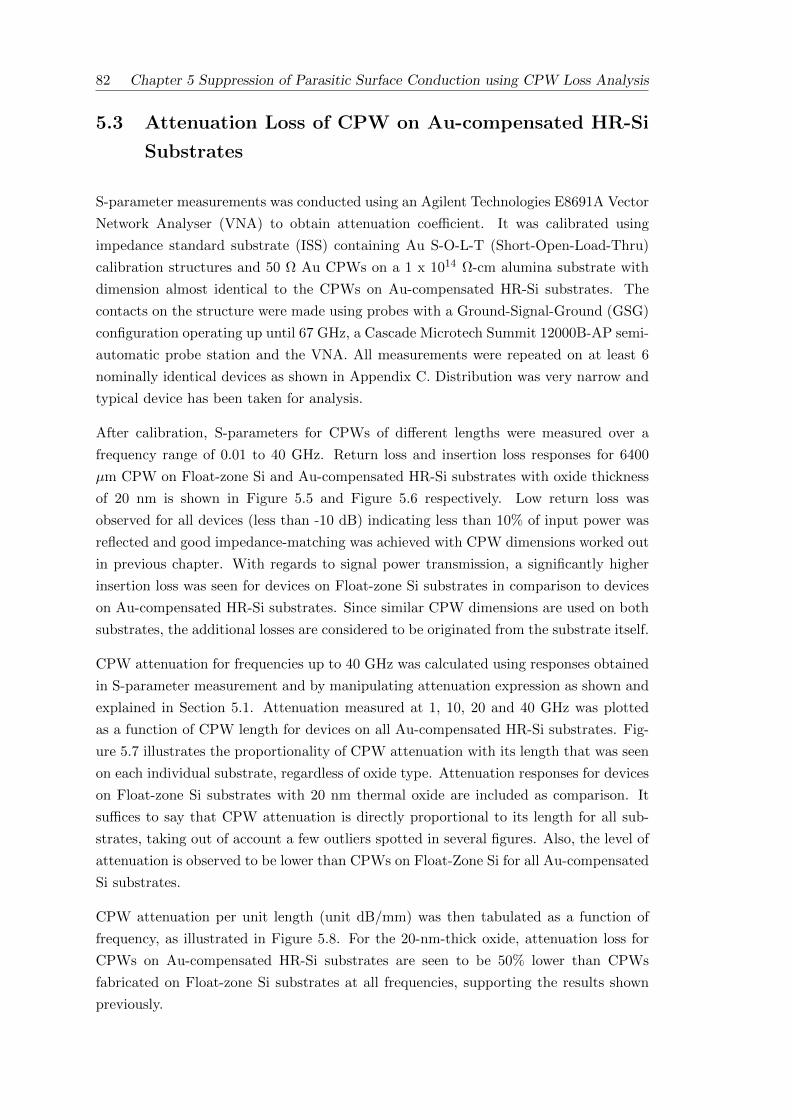
82 Chapter 5 Suppression of Parasitic Surface Conduction using CPW Loss Analysis
5.3 Attenuation Loss of CPW on Au-compensated HR-Si
Substrates
S-parameter measurements was conducted using an Agilent Technologies E8691A Vector
Network Analyser (VNA) to obtain attenuation coefficient. It was calibrated using
impedance standard substrate (ISS) containing Au S-O-L-T (Short-Open-Load-Thru)
calibration structures and 50 Ω Au CPWs on a 1 x 10¹⁴ Ω-cm alumina substrate with
dimension almost identical to the CPWs on Au-compensated HR-Si substrates. The
contacts on the structure were made using probes with a Ground-Signal-Ground (GSG)
configuration operating up until 67 GHz, a Cascade Microtech Summit 12000B-AP semi-
automatic probe station and the VNA. All measurements were repeated on at least 6
nominally identical devices as shown in Appendix C. Distribution was very narrow and
typical device has been taken for analysis.
After calibration, S-parameters for CPWs of different lengths were measured over a
frequency range of 0.01 to 40 GHz. Return loss and insertion loss responses for 6400
µm CPW on Float-zone Si and Au-compensated HR-Si substrates with oxide thickness
of 20 nm is shown in Figure 5.5 and Figure 5.6 respectively. Low return loss was
observed for all devices (less than -10 dB) indicating less than 10% of input power was
reflected and good impedance-matching was achieved with CPW dimensions worked out
in previous chapter. With regards to signal power transmission, a significantly higher
insertion loss was seen for devices on Float-zone Si substrates in comparison to devices
on Au-compensated HR-Si substrates. Since similar CPW dimensions are used on both
substrates, the additional losses are considered to be originated from the substrate itself.
CPW attenuation for frequencies up to 40 GHz was calculated using responses obtained
in S-parameter measurement and by manipulating attenuation expression as shown and
explained in Section 5.1. Attenuation measured at 1, 10, 20 and 40 GHz was plotted
as a function of CPW length for devices on all Au-compensated HR-Si substrates. Fig-
ure 5.7 illustrates the proportionality of CPW attenuation with its length that was seen
on each individual substrate, regardless of oxide type. Attenuation responses for devices
on Float-zone Si substrates with 20 nm thermal oxide are included as comparison. It
suffices to say that CPW attenuation is directly proportional to its length for all sub-
strates, taking out of account a few outliers spotted in several figures. Also, the level of
attenuation is observed to be lower than CPWs on Float-Zone Si for all Au-compensated
Si substrates.
CPW attenuation per unit length (unit dB/mm) was then tabulated as a function of
frequency, as illustrated in Figure 5.8. For the 20-nm-thick oxide, attenuation loss for
CPWs on Au-compensated HR-Si substrates are seen to be 50% lower than CPWs
fabricated on Float-zone Si substrates at all frequencies, supporting the results shown
previously.
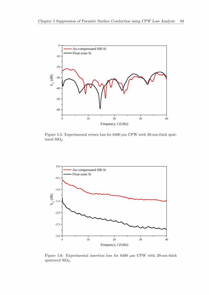
Chapter 5 Suppression of Parasitic Surface Conduction using CPW Loss Analysis 83
0 1 0 2 0 3 0 4 0
- 6 0
- 5 0
- 4 0
- 3 0
- 2 0
- 1 0
0S 11 (
dB)
F r e q u e n c y , f ( G H z )
A u - c o m p e n s a t e d H R - S i F l o a t - z o n e S i
Figure 5.5: Experimental return loss for 6400 µm CPW with 20-nm-thick sput-tered SiO2.
0 1 0 2 0 3 0 4 0- 3 . 0
- 2 . 5
- 2 . 0
- 1 . 5
- 1 . 0
- 0 . 5
0 . 0
S 21 (dB
)
F r e q u e n c y , f ( G H z )
A u - c o m p e n s a t e d H R - S i F l o a t - z o n e S i
Figure 5.6: Experimental insertion loss for 6400 µm CPW with 20-nm-thicksputtered SiO2.
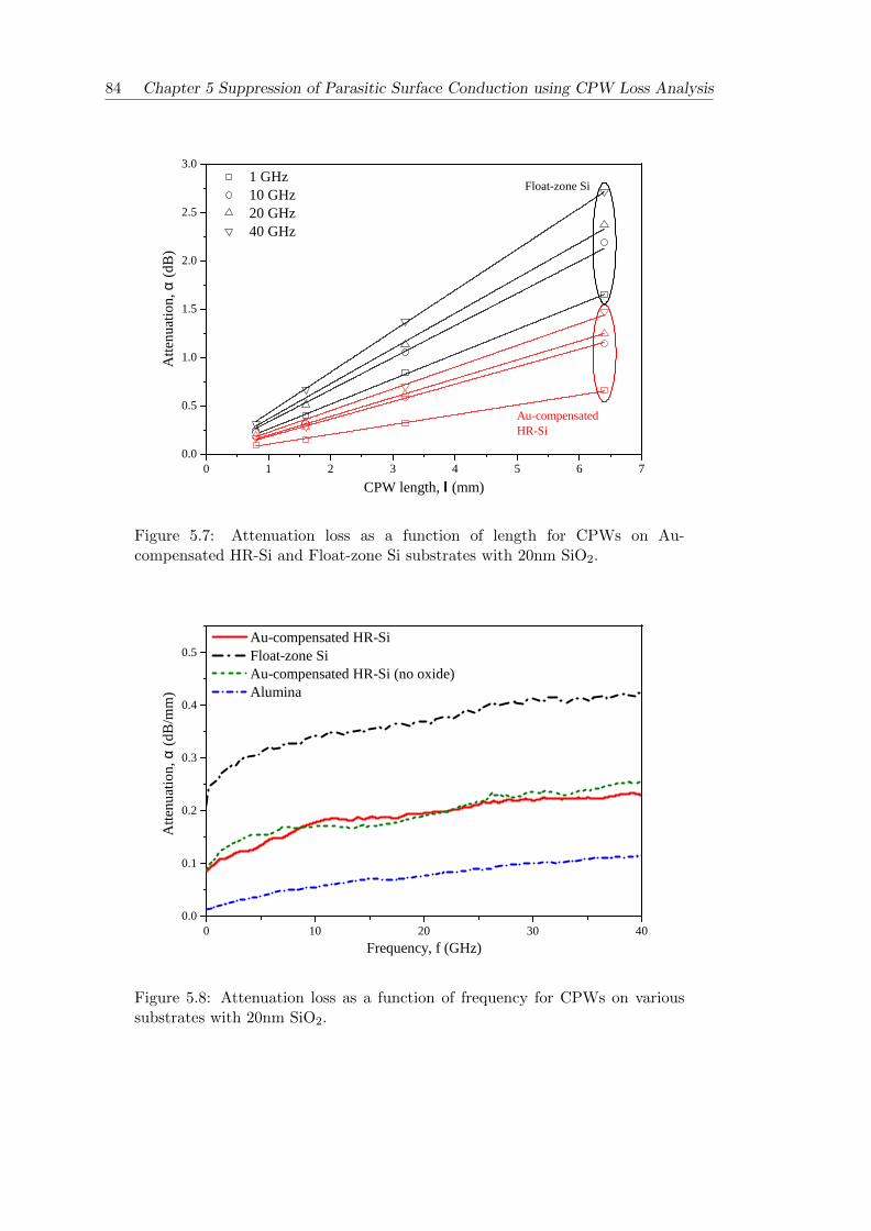
84 Chapter 5 Suppression of Parasitic Surface Conduction using CPW Loss Analysis
0 1 2 3 4 5 6 70 . 0
0 . 5
1 . 0
1 . 5
2 . 0
2 . 5
3 . 0
A u - c o m p e n s a t e d H R - S i
1 G H z 1 0 G H z 2 0 G H z 4 0 G H z
Attenu
ation, α
(dB)
C P W l e n g t h , l ( m m )
F l o a t - z o n e S i
Figure 5.7: Attenuation loss as a function of length for CPWs on Au-compensated HR-Si and Float-zone Si substrates with 20nm SiO2.
0 1 0 2 0 3 0 4 00 . 0
0 . 1
0 . 2
0 . 3
0 . 4
0 . 5 A u - c o m p e n s a t e d H R - S i F l o a t - z o n e S i A u - c o m p e n s a t e d H R - S i ( n o o x i d e ) A l u m i n a
Attenu
ation, α
(dB/m
m)
F r e q u e n c y , f ( G H z )
Figure 5.8: Attenuation loss as a function of frequency for CPWs on varioussubstrates with 20nm SiO2.
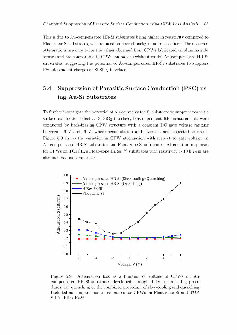
Chapter 5 Suppression of Parasitic Surface Conduction using CPW Loss Analysis 85
This is due to Au-compensated HR-Si substrates being higher in resistivity compared to
Float-zone Si substrates, with reduced number of background free carriers. The observed
attenuations are only twice the values obtained from CPWs fabricated on alumina sub-
strates and are comparable to CPWs on naked (without oxide) Au-compensated HR-Si
substrates, suggesting the potential of Au-compensated HR-Si substrates to suppress
PSC-dependent charges at Si-SiO2 interface.
5.4 Suppression of Parasitic Surface Conduction (PSC) us-
ing Au-Si Substrates
To further investigate the potential of Au-compensated Si substrate to suppress parasitic
surface conduction effect at Si-SiO2 interface, bias-dependent RF measurements were
conducted by back-biasing CPW structure with a constant DC gate voltage ranging
between +6 V and -6 V, where accumulation and inversion are suspected to occur.
Figure 5.9 shows the variation in CPW attenuation with respect to gate voltage on
Au-compensated HR-Si substrates and Float-zone Si substrates. Attenuation responses
for CPWs on TOPSIL’s Float-zone HiResTM substrates with resistivity > 10 kΩ-cm are
also included as comparison.
- 6 - 4 - 2 0 2 4 60 . 00 . 10 . 20 . 30 . 40 . 50 . 60 . 70 . 80 . 91 . 0
Attenu
ation, α
(dB/m
m)
V o l t a g e , V ( V )
A u - c o m p e n s a t e d H R - S i ( S l o w - c o o l i n g + Q u e n c h i n g ) A u - c o m p e n s a t e d H R - S i ( Q u e n c h i n g ) H i R e s F z - S i F l o a t - z o n e S i
Figure 5.9: Attenuation loss as a function of voltage of CPWs on Au-compensated HR-Si substrates developed through different annealing proce-dures, i.e. quenching or the combined procedure of slow-cooling and quenching.Included as comparisons are responses for CPWs on Float-zone Si and TOP-SIL’s HiRes Fz-Si.
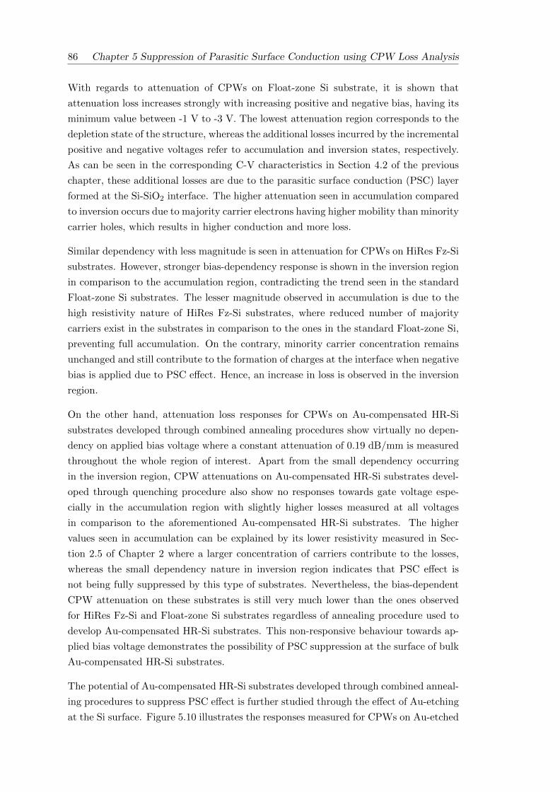
86 Chapter 5 Suppression of Parasitic Surface Conduction using CPW Loss Analysis
With regards to attenuation of CPWs on Float-zone Si substrate, it is shown that
attenuation loss increases strongly with increasing positive and negative bias, having its
minimum value between -1 V to -3 V. The lowest attenuation region corresponds to the
depletion state of the structure, whereas the additional losses incurred by the incremental
positive and negative voltages refer to accumulation and inversion states, respectively.
As can be seen in the corresponding C-V characteristics in Section 4.2 of the previous
chapter, these additional losses are due to the parasitic surface conduction (PSC) layer
formed at the Si-SiO2 interface. The higher attenuation seen in accumulation compared
to inversion occurs due to majority carrier electrons having higher mobility than minority
carrier holes, which results in higher conduction and more loss.
Similar dependency with less magnitude is seen in attenuation for CPWs on HiRes Fz-Si
substrates. However, stronger bias-dependency response is shown in the inversion region
in comparison to the accumulation region, contradicting the trend seen in the standard
Float-zone Si substrates. The lesser magnitude observed in accumulation is due to the
high resistivity nature of HiRes Fz-Si substrates, where reduced number of majority
carriers exist in the substrates in comparison to the ones in the standard Float-zone Si,
preventing full accumulation. On the contrary, minority carrier concentration remains
unchanged and still contribute to the formation of charges at the interface when negative
bias is applied due to PSC effect. Hence, an increase in loss is observed in the inversion
region.
On the other hand, attenuation loss responses for CPWs on Au-compensated HR-Si
substrates developed through combined annealing procedures show virtually no depen-
dency on applied bias voltage where a constant attenuation of 0.19 dB/mm is measured
throughout the whole region of interest. Apart from the small dependency occurring
in the inversion region, CPW attenuations on Au-compensated HR-Si substrates devel-
oped through quenching procedure also show no responses towards gate voltage espe-
cially in the accumulation region with slightly higher losses measured at all voltages
in comparison to the aforementioned Au-compensated HR-Si substrates. The higher
values seen in accumulation can be explained by its lower resistivity measured in Sec-
tion 2.5 of Chapter 2 where a larger concentration of carriers contribute to the losses,
whereas the small dependency nature in inversion region indicates that PSC effect is
not being fully suppressed by this type of substrates. Nevertheless, the bias-dependent
CPW attenuation on these substrates is still very much lower than the ones observed
for HiRes Fz-Si and Float-zone Si substrates regardless of annealing procedure used to
develop Au-compensated HR-Si substrates. This non-responsive behaviour towards ap-
plied bias voltage demonstrates the possibility of PSC suppression at the surface of bulk
Au-compensated HR-Si substrates.
The potential of Au-compensated HR-Si substrates developed through combined anneal-
ing procedures to suppress PSC effect is further studied through the effect of Au-etching
at the Si surface. Figure 5.10 illustrates the responses measured for CPWs on Au-etched
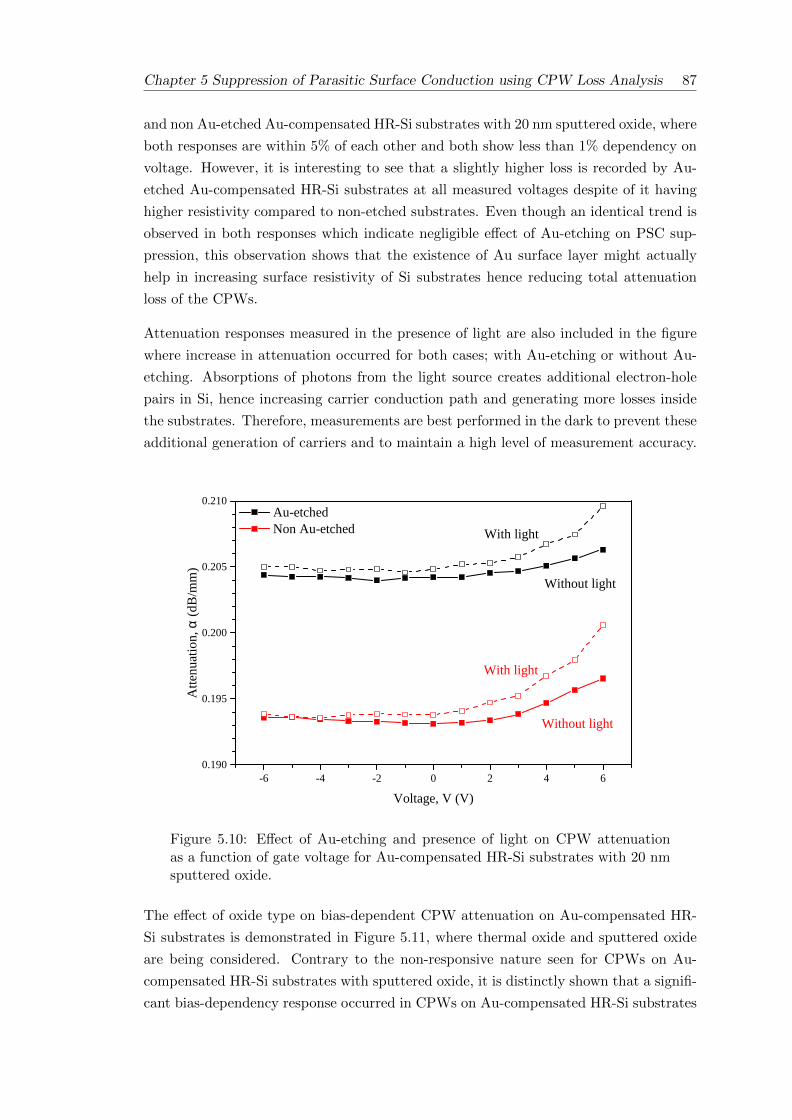
Chapter 5 Suppression of Parasitic Surface Conduction using CPW Loss Analysis 87
and non Au-etched Au-compensated HR-Si substrates with 20 nm sputtered oxide, where
both responses are within 5% of each other and both show less than 1% dependency on
voltage. However, it is interesting to see that a slightly higher loss is recorded by Au-
etched Au-compensated HR-Si substrates at all measured voltages despite of it having
higher resistivity compared to non-etched substrates. Even though an identical trend is
observed in both responses which indicate negligible effect of Au-etching on PSC sup-
pression, this observation shows that the existence of Au surface layer might actually
help in increasing surface resistivity of Si substrates hence reducing total attenuation
loss of the CPWs.
Attenuation responses measured in the presence of light are also included in the figure
where increase in attenuation occurred for both cases; with Au-etching or without Au-
etching. Absorptions of photons from the light source creates additional electron-hole
pairs in Si, hence increasing carrier conduction path and generating more losses inside
the substrates. Therefore, measurements are best performed in the dark to prevent these
additional generation of carriers and to maintain a high level of measurement accuracy.
- 6 - 4 - 2 0 2 4 60 . 1 9 0
0 . 1 9 5
0 . 2 0 0
0 . 2 0 5
0 . 2 1 0
W i t h o u t l i g h t
W i t h l i g h t
W i t h o u t l i g h t
Attenu
ation, α
(dB/m
m)
V o l t a g e , V ( V )
A u - e t c h e d N o n A u - e t c h e d
W i t h l i g h t
Figure 5.10: Effect of Au-etching and presence of light on CPW attenuationas a function of gate voltage for Au-compensated HR-Si substrates with 20 nmsputtered oxide.
The effect of oxide type on bias-dependent CPW attenuation on Au-compensated HR-
Si substrates is demonstrated in Figure 5.11, where thermal oxide and sputtered oxide
are being considered. Contrary to the non-responsive nature seen for CPWs on Au-
compensated HR-Si substrates with sputtered oxide, it is distinctly shown that a signifi-
cant bias-dependency response occurred in CPWs on Au-compensated HR-Si substrates
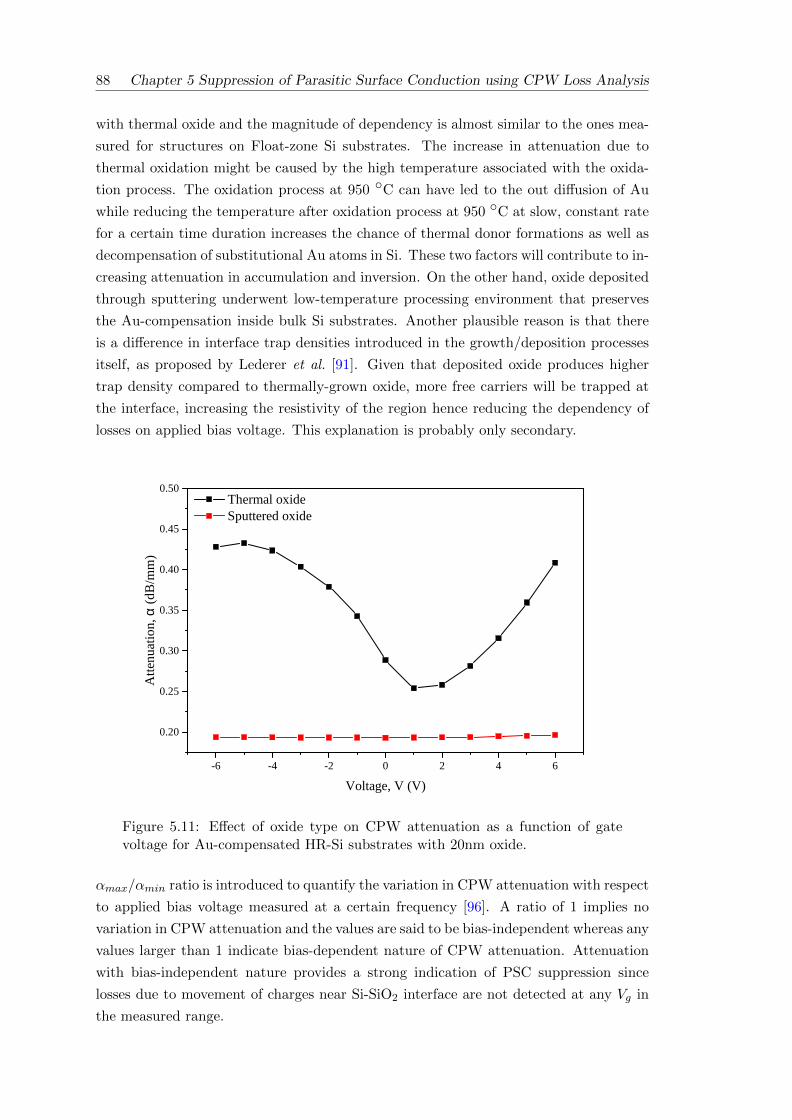
88 Chapter 5 Suppression of Parasitic Surface Conduction using CPW Loss Analysis
with thermal oxide and the magnitude of dependency is almost similar to the ones mea-
sured for structures on Float-zone Si substrates. The increase in attenuation due to
thermal oxidation might be caused by the high temperature associated with the oxida-
tion process. The oxidation process at 950 C can have led to the out diffusion of Au
while reducing the temperature after oxidation process at 950 C at slow, constant rate
for a certain time duration increases the chance of thermal donor formations as well as
decompensation of substitutional Au atoms in Si. These two factors will contribute to in-
creasing attenuation in accumulation and inversion. On the other hand, oxide deposited
through sputtering underwent low-temperature processing environment that preserves
the Au-compensation inside bulk Si substrates. Another plausible reason is that there
is a difference in interface trap densities introduced in the growth/deposition processes
itself, as proposed by Lederer et al. [91]. Given that deposited oxide produces higher
trap density compared to thermally-grown oxide, more free carriers will be trapped at
the interface, increasing the resistivity of the region hence reducing the dependency of
losses on applied bias voltage. This explanation is probably only secondary.
- 6 - 4 - 2 0 2 4 6
0 . 2 0
0 . 2 5
0 . 3 0
0 . 3 5
0 . 4 0
0 . 4 5
0 . 5 0
Attenu
ation, α
(dB/m
m)
V o l t a g e , V ( V )
T h e r m a l o x i d e S p u t t e r e d o x i d e
Figure 5.11: Effect of oxide type on CPW attenuation as a function of gatevoltage for Au-compensated HR-Si substrates with 20nm oxide.
αmax/αmin ratio is introduced to quantify the variation in CPW attenuation with respect
to applied bias voltage measured at a certain frequency [96]. A ratio of 1 implies no
variation in CPW attenuation and the values are said to be bias-independent whereas any
values larger than 1 indicate bias-dependent nature of CPW attenuation. Attenuation
with bias-independent nature provides a strong indication of PSC suppression since
losses due to movement of charges near Si-SiO2 interface are not detected at any Vg in
the measured range.
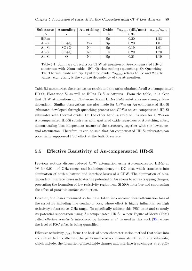
Chapter 5 Suppression of Parasitic Surface Conduction using CPW Loss Analysis 89
Substrate Annealing Au-etching Oxide *αmeas (dB/mm) αmax/αminFz - - Th 0.34 3
HiRes - - Sp 0.20 1.53
Au-Si SC+Q Yes Sp 0.20 1.01
Au-Si SC+Q No Sp 0.19 1.01
Au-Si SC+Q No Th 0.29 1.70
Au-Si Q No Sp 0.21 1.19
Table 5.1: Summary of results for CPW attenuation on Au-compensated HR-Sisubstrates with 20nm oxide. SC+Q: slow-cooling+quenching; Q: Quenching;Th: Thermal oxide and Sp: Sputtered oxide. *αmeas relates to 0V and 20GHzvalues. αmax/αmin is the voltage dependency of the attenuation.
Table 5.1 summarises the attenuation results and the ratios obtained for all Au-compensated
HR-Si, Float-zone Si as well as HiRes Fz-Si substrates. From the table, it is clear
that CPW attenuations on Float-zone Si and HiRes Fz-Si substrates are strongly bias-
dependent. Similar observations are also made for CPWs on Au-compensated HR-Si
substrates developed through quenching process and CPWs on Au-compensated HR-Si
substrates with thermal oxide. On the other hand, a ratio of 1 is seen for CPWs on
Au-compensated HR-Si substrates with sputtered oxide regardless of Au-etching effect,
demonstrating bias-independent nature of the structure, together with the lowest ac-
tual attenuation. Therefore, it can be said that Au-compensated HR-Si substrates can
potentially suppressed PSC effect at the bulk Si surface.
5.5 Effective Resistivity of Au-compensated HR-Si
Previous sections discuss reduced CPW attenuation using Au-compensated HR-Si at
0V for 0.01 - 40 GHz range, and its independency on DC bias, which translates into
elimination of both substrate and interface losses of a CPW. The elimination of bias-
dependent interface losses indicates the potential of Au atoms to act as trapping charges,
preventing the formation of low resistivity region near Si-SiO2 interface and suppressing
the effect of parasitic surface conduction.
However, the losses measured so far have taken into account total attenuation loss of
the structure including line conductor loss, whose effect is highly influential on high
resistivity substrate at GHz range. To specifically address this PSC issue and to study
its potential suppression using Au-compensated HR-Si, a new Figure-of-Merit (FoM)
called effective resistivity introduced by Lederer et al. is used in this work [35], where
the level of PSC effect is being quantified.
Effective resistivity, ρeff forms the basis of a new characterisation method that takes into
account all factors affecting the performance of a coplanar structure on a Si substrate,
which include, the formation of fixed oxide charges and interface trap charges at Si-SiO2
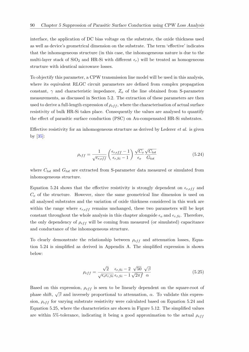
90 Chapter 5 Suppression of Parasitic Surface Conduction using CPW Loss Analysis
interface, the application of DC bias voltage on the substrate, the oxide thickness used
as well as device’s geometrical dimension on the substrate. The term ‘effective’ indicates
that the inhomogeneous structure (in this case, the inhomogeneous nature is due to the
multi-layer stack of SiO2 and HR-Si with different εr) will be treated as homogeneous
structure with identical microwave losses.
To objectify this parameter, a CPW transmission line model will be used in this analysis,
where its equivalent RLGC circuit parameters are defined from complex propagation
constant, γ and characteristic impedance, Zo of the line obtained from S-parameter
measurements, as discussed in Section 5.2. The extraction of these parameters are then
used to derive a full-length expression of ρeff , where the characterisation of actual surface
resistivity of bulk HR-Si takes place. Consequently the values are analysed to quantify
the effect of parasitic surface conduction (PSC) on Au-compensated HR-Si substrates.
Effective resistivity for an inhomogeneous structure as derived by Lederer et al. is given
by [35]:
ρeff =1
√εr,eff
(εr,eff − 1
εr,Si − 1
) √Coεo
√CtotGtot
(5.24)
where Ctot and Gtot are extracted from S-parameter data measured or simulated from
inhomogeneous structure.
Equation 5.24 shows that the effective resistivity is strongly dependent on εr,eff and
Co of the structure. However, since the same geometrical line dimension is used on
all analysed substrates and the variation of oxide thickness considered in this work are
within the range where εr,eff remains unchanged, these two parameters will be kept
constant throughout the whole analysis in this chapter alongside εo and εr,Si. Therefore,
the only dependency of ρeff will be coming from measured (or simulated) capacitance
and conductance of the inhomogeneous structure.
To clearly demonstrate the relationship between ρeff and attenuation losses, Equa-
tion 5.24 is simplified as derived in Appendix A. The simplified expression is shown
below:
ρeff =
√2
√εoεr,Si
εr,Si − 2
εr,Si − 1
√50√
2πf
√β
α(5.25)
Based on this expression, ρeff is seen to be linearly dependent on the square-root of
phase shift,√β and inversely proportional to attenuation, α. To validate this expres-
sion, ρeff for varying substrate resistivity were calculated based on Equation 5.24 and
Equation 5.25, where the characteristics are shown in Figure 5.12. The simplified values
are within 5%-tolerance, indicating it being a good approximation to the actual ρeff
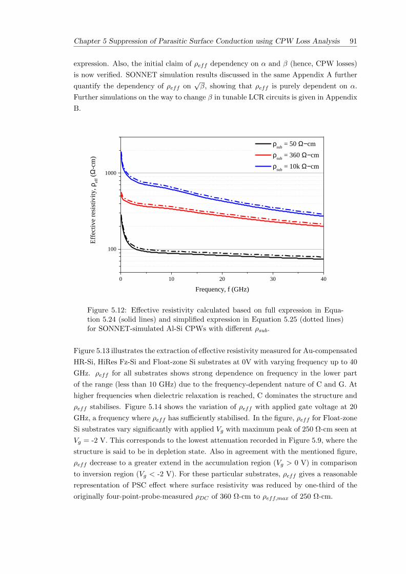
Chapter 5 Suppression of Parasitic Surface Conduction using CPW Loss Analysis 91
expression. Also, the initial claim of ρeff dependency on α and β (hence, CPW losses)
is now verified. SONNET simulation results discussed in the same Appendix A further
quantify the dependency of ρeff on√β, showing that ρeff is purely dependent on α.
Further simulations on the way to change β in tunable LCR circuits is given in Appendix
B.
0 1 0 2 0 3 0 4 0
1 0 0
1 0 0 0
Effect
ive res
istivit
y, ρeff
(Ω-cm
)
F r e q u e n c y , f ( G H z )
ρ s u b = 5 0 Ω− c m ρ s u b = 3 6 0 Ω− c m ρ s u b = 1 0 k Ω− c m
Figure 5.12: Effective resistivity calculated based on full expression in Equa-tion 5.24 (solid lines) and simplified expression in Equation 5.25 (dotted lines)for SONNET-simulated Al-Si CPWs with different ρsub.
Figure 5.13 illustrates the extraction of effective resistivity measured for Au-compensated
HR-Si, HiRes Fz-Si and Float-zone Si substrates at 0V with varying frequency up to 40
GHz. ρeff for all substrates shows strong dependence on frequency in the lower part
of the range (less than 10 GHz) due to the frequency-dependent nature of C and G. At
higher frequencies when dielectric relaxation is reached, C dominates the structure and
ρeff stabilises. Figure 5.14 shows the variation of ρeff with applied gate voltage at 20
GHz, a frequency where ρeff has sufficiently stabilised. In the figure, ρeff for Float-zone
Si substrates vary significantly with applied Vg with maximum peak of 250 Ω-cm seen at
Vg = -2 V. This corresponds to the lowest attenuation recorded in Figure 5.9, where the
structure is said to be in depletion state. Also in agreement with the mentioned figure,
ρeff decrease to a greater extend in the accumulation region (Vg > 0 V) in comparison
to inversion region (Vg < -2 V). For these particular substrates, ρeff gives a reasonable
representation of PSC effect where surface resistivity was reduced by one-third of the
originally four-point-probe-measured ρDC of 360 Ω-cm to ρeff,max of 250 Ω-cm.
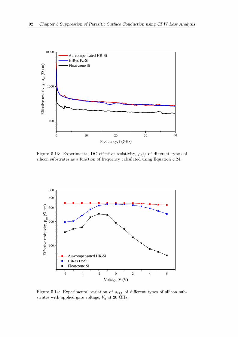
92 Chapter 5 Suppression of Parasitic Surface Conduction using CPW Loss Analysis
0 1 0 2 0 3 0 4 0
1 0 0
1 0 0 0
1 0 0 0 0
Effect
ive res
istivit
y, ρeff
(Ω-cm
)
F r e q u e n c y , f ( G H z )
A u - c o m p e n s a t e d H R - S i H i R e s F z - S i F l o a t - z o n e S i
Figure 5.13: Experimental DC effective resistivity, ρeff of different types ofsilicon substrates as a function of frequency calculated using Equation 5.24.
- 6 - 4 - 2 0 2 4 6
1 0 0
2 0 0
3 0 0
4 0 05 0 0
Effect
ive res
istivit
y, ρeff
(Ω-cm
)
V o l t a g e , V ( V )
A u - c o m p e n s a t e d H R - S i H i R e s F z - S i F l o a t - z o n e S i
Figure 5.14: Experimental variation of ρeff of different types of silicon sub-strates with applied gate voltage, Vg at 20 GHz.
Chapter 5 Suppression of Parasitic Surface Conduction using CPW Loss Analysis 93
Meanwhile, ρeff for HiRes Fz-Si substrates show an extreme reduction from ρDC of
nominally 10 kΩ-cm to ρeff,max of only 330 Ω-cm between -1 V to 1 V, even though the
trend corresponds to the reciprocal of bias-dependent attenuation shown in Figure 5.9.
Similar observation is made for ρeff of Au-compensated HR-Si where the values are very
much less than the measured ρDC but with no dependency recorded as portrayed in the
same previously mentioned figure. The reason for this discrepancy is related to the high
resistivity nature of HiRes Fz-Si and Au-compensated HR-Si substrate and contact probe
sensitivity during S-parameter measurement [97]. At very high frequencies, parasitic
series resistance becomes comparable to substrate’s bulk resistance hence a very sensitive
probing method needed to be incorporated to obtain the accurate value of C and G.
Nevertheless, the trends shown by these three substrates provide the rough idea on how
PSC regulates the resistivity of bulk Si substrates. When gate voltage is applied, the
induced PSC-dependent charges at the Si surface introduce a low resistivity region in
between oxide and Si substrates. Depending on the magnitude and polarity of Vg, the
existence of low resistivity region at the interface reduces the effective resistivity of Si
bulk structure and increases the total microwave losses. With relation to the responses
seen in the figure, significant dependency of ρeff on Vg can be seen for Float-zone Si
and HiRes Fz-Si substrates, which are directly translated to substrates’ dependency on
PSC whereas the flat, stabilised ρeff values seen for Au-compensated HR-Si substrates
indicate the non-responsive nature of Au-compensated HR-Si substrates towards PSC.
5.6 Summary
Microwave characteristics of conductor-backed coplanar waveguides on Au-compensated
Hr-Si substrates were measured under DC bias influence to observe potential PSC sup-
pression at microwave frequency range, where the effect is most prominent. Full sup-
pression of PSC-dependent charges is seen for non Au-etched, Au-compensated HR-Si
substrates developed through combined annealing procedure with constant attenuation
of 0.19 dB/mm is measured throughout the whole voltage range at 20 GHz to give a
unity αmax/αmin ratio. Similar non-dependency nature is not observed for compensated
substrates developed through single annealing procedure, with αmax/αmin value larger
than 1 was calculated at the same frequency. Therefore it is shown that the combined
annealing procedure provides higher density of traps inside Si substrate in comparison
to substrates developed through single quenching procedure. Meanwhile, the effect of
Au-etching on suppression of PSC was also observed, in which it demonstrates similar
non-dependency nature but with higher attenuation level of 0.21 dB/mm at 20 GHz.
Therefore, Au-etching step in fabrication of devices for microwave application can be
neglected to improve microwave performance as well as to reduce complexity of fabrica-
tion process. In addition to that, oxide type also plays an important role in suppressing
94 Chapter 5 Suppression of Parasitic Surface Conduction using CPW Loss Analysis
PSC effect on Au-compensated HR-Si substrates. Thermal oxide is seen to be incom-
patible to be used as oxide passivation layer due to its high processing temperature
which has caused abruptions in compensated Au behaviour. As a result, bias-dependent
attenuation characteristics for substrates with thermal oxide are shown to be of similar
trend to the ones observed in Float-zone Si and have αmax/αmin ratio as high as the
one calculated for HiRes Fz-Si substrates. Meanwhile, the extraction of substrate’s ef-
fective resistivity show major discrepancy value-wise, however, the trend illustrated on
bias-dependent effective resistivity characteristics for Au-compensated HR-Si substrates
is in agreement to the previously discussed results, in which a constant value of ρeff
is calculated throughout the whole voltage range, demonstrating suppression effect on
PSC using these particular substrates.
Chapter 6
Improving Quality Factor of
Meander Inductors
The potential of Au-compensated HR-Si substrates to suppress parasitic surface con-
duction effect was successfully shown in the previous chapter, where attenuation charac-
teristics of conductor-backed coplanar waveguides were used as the tool to observe and
quantify the reduced effect of PSC using high resistivity substrates developed through
deep-level doping compensation method. In this chapter, Au-compensated HR-Si sub-
strates will be used as the base substrate for the initial development of 3D-integrated
passive components in Si-based MMICs technology. Taken as the most straighforward
passive device to be designed and analysed, meander inductors were chosen. It has sev-
eral advantages in comparison to spiral structures including reduced level of lithography
(with only one metal layer required) and reduced amount of mutual inductance due to
its uni-directional current. The ability of this structure to provide an accurate repre-
sentation of material properties especially in the near-surface region becomes the solid
basis of using this particular structure in this work, where potential PSC suppression
using Au-compensated HR-Si substrate for microwave application is being studied.
Q-factor analysis is used to characterise the performance of meander inductors on ox-
idised Au-compensated HR-Si substrates, where microwave measurements were con-
ducted for extraction of S-parameter data. To start, this chapter will discuss the theory
and extraction of Q factor from S-parameter data. It will be followed by experimental
analysis and discussion on the extracted Q-factor parameter.
95
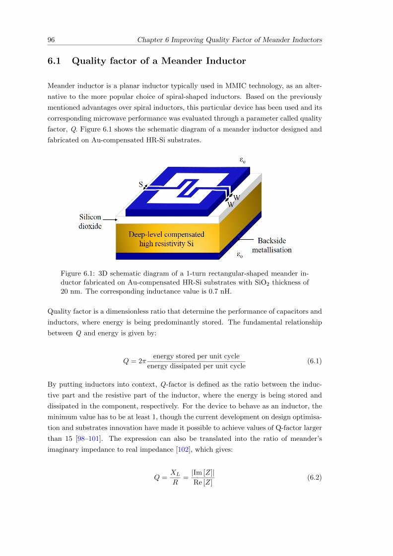
96 Chapter 6 Improving Quality Factor of Meander Inductors
6.1 Quality factor of a Meander Inductor
Meander inductor is a planar inductor typically used in MMIC technology, as an alter-
native to the more popular choice of spiral-shaped inductors. Based on the previously
mentioned advantages over spiral inductors, this particular device has been used and its
corresponding microwave performance was evaluated through a parameter called quality
factor, Q. Figure 6.1 shows the schematic diagram of a meander inductor designed and
fabricated on Au-compensated HR-Si substrates.
Figure 6.1: 3D schematic diagram of a 1-turn rectangular-shaped meander in-ductor fabricated on Au-compensated HR-Si substrates with SiO2 thickness of20 nm. The corresponding inductance value is 0.7 nH.
Quality factor is a dimensionless ratio that determine the performance of capacitors and
inductors, where energy is being predominantly stored. The fundamental relationship
between Q and energy is given by:
Q = 2πenergy stored per unit cycle
energy dissipated per unit cycle(6.1)
By putting inductors into context, Q-factor is defined as the ratio between the induc-
tive part and the resistive part of the inductor, where the energy is being stored and
dissipated in the component, respectively. For the device to behave as an inductor, the
minimum value has to be at least 1, though the current development on design optimisa-
tion and substrates innovation have made it possible to achieve values of Q-factor larger
than 15 [98–101]. The expression can also be translated into the ratio of meander’s
imaginary impedance to real impedance [102], which gives:
Q =XL
R=|Im [Z]|Re [Z]
(6.2)
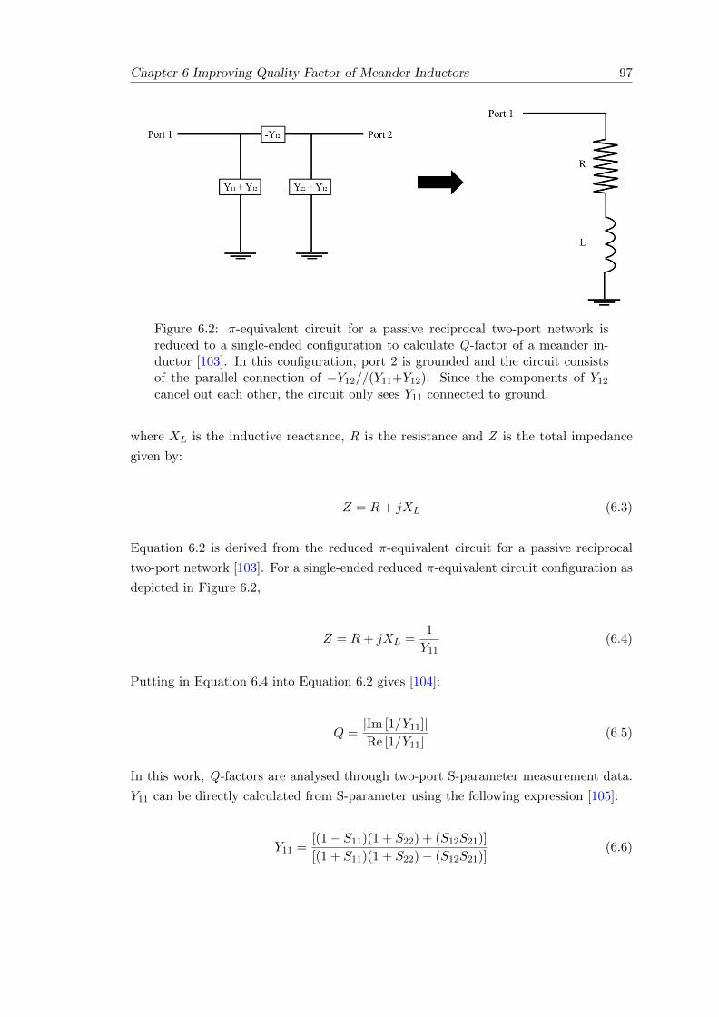
Chapter 6 Improving Quality Factor of Meander Inductors 97
Figure 6.2: π-equivalent circuit for a passive reciprocal two-port network isreduced to a single-ended configuration to calculate Q-factor of a meander in-ductor [103]. In this configuration, port 2 is grounded and the circuit consistsof the parallel connection of −Y12//(Y11+Y12). Since the components of Y12cancel out each other, the circuit only sees Y11 connected to ground.
where XL is the inductive reactance, R is the resistance and Z is the total impedance
given by:
Z = R+ jXL (6.3)
Equation 6.2 is derived from the reduced π-equivalent circuit for a passive reciprocal
two-port network [103]. For a single-ended reduced π-equivalent circuit configuration as
depicted in Figure 6.2,
Z = R+ jXL =1
Y11(6.4)
Putting in Equation 6.4 into Equation 6.2 gives [104]:
Q =|Im [1/Y11]|Re [1/Y11]
(6.5)
In this work, Q-factors are analysed through two-port S-parameter measurement data.
Y11 can be directly calculated from S-parameter using the following expression [105]:
Y11 =[(1− S11)(1 + S22) + (S12S21)]
[(1 + S11)(1 + S22)− (S12S21)](6.6)
98 Chapter 6 Improving Quality Factor of Meander Inductors
6.2 S-parameter Measurement Setup & Results
To calculate Q-factor of meander inductor and consequently evaluate its performance
on Au-compensated HR-Si substrates, S-parameter measurements were conducted on
all fabricated structures mentioned in Section 3.3 of Chapter 3 using Agilent Technolo-
gies E8691A Vector Network Analyser (VNA). The calibration setup for this measure-
ment was the same as the one required for CPW attenuation loss measurement (refer
Section 5.3 in Chapter 5). After calibration, S-parameter responses for all fabricated
meander inductors were measured over a frequency range of 0.01 - 40 GHz.
Return loss for meander inductors fabricated on Au-compensated HR-Si and Float-zone
Si substrates are shown in Figure 6.3 to Figure 6.7. The recorded values are in good
agreement with SONNET simulation for all inductance values and structures. These
observations confirm that at least 30% of power is being reflected back to the port by
the devices, regardless of the shape of meander turns or tapering options used. It shows
that high level of impedance-mismatching still occurs and further optimisation needs to
be done on the design to improve this.
0 1 0 2 0 3 0 4 0- 7 0
- 6 0
- 5 0
- 4 0
- 3 0
- 2 0
- 1 0
0
S O N N E T
S 11 (dB
)
F r e q u e n c y , f ( G H z )
R e c t a n g u l a r R e c t a n g u l a r , T a p e r e d R o u n d R o u n d , T a p e r e d
A u - c o m p e n s a t e d H R - S i
F l o a t - z o n e S i
Figure 6.3: SONNET-simulated and measured return loss of 0.7 nH meanderinductors on Float-zone Si and Au-compensated HR-Si substrates. Curves re-flecting different shapes of the inductor result in near identical curves and arenot individually visible.
Chapter 6 Improving Quality Factor of Meander Inductors 99
0 1 0 2 0 3 0 4 0- 4 0
- 3 0
- 2 0
- 1 0
0
S O N N E T
F l o a t - z o n e S i
A u - c o m p e n s a t e d H R - S i
S 11 (dB
)
F r e q u e n c y , f ( G H z )
R e c t a n g u l a r R e c t a n g u l a r , T a p e r e d R o u n d R o u n d , T a p e r e d
Figure 6.4: SONNET-simulated and measured return loss of 1.25 nH meanderinductors on Float-zone Si and Au-compensated HR-Si substrates. Curves re-flecting different shapes of the inductor result in near identical curves and arenot individually visible.
0 1 0 2 0 3 0 4 0
- 3 0
- 2 0
- 1 0
0
S O N N E T
F l o a t - z o n e S i
A u - c o m p e n s a t e d H R - S i
S 11 (dB
)
F r e q u e n c y , f ( G H z )
R e c t a n g u l a r R e c t a n g u l a r , T a p e r e d R o u n d R o u n d , T a p e r e d
Figure 6.5: SONNET-simulated and measured return loss of 1.61 nH meanderinductors on Float-zone Si and Au-compensated HR-Si substrates. Curves re-flecting different shapes of the inductor result in near identical curves and arenot individually visible.
100 Chapter 6 Improving Quality Factor of Meander Inductors
0 1 0 2 0 3 0 4 0- 3 0
- 2 0
- 1 0
0
S O N N E TF l o a t - z o n e S i
A u - c o m p e n s a t e d H R - S i
S 11 (dB
)
F r e q u e n c y , f ( G H z )
R e c t a n g u l a r , T a p e r e d R o u n d , T a p e r e d
Figure 6.6: SONNET-simulated and measured return loss of 2.08 nH meanderinductors on Float-zone Si and Au-compensated HR-Si substrates. Curves re-flecting different shapes of the inductor result in near identical curves and arenot individually visible.
0 1 0 2 0 3 0 4 0- 3 0
- 2 0
- 1 0
0
S O N N E TF l o a t - z o n e S i
A u - c o m p e n s a t e d H R - S i
S 11 (dB
)
F r e q u e n c y , f ( G H z )
R e c t a n g u l a r , T a p e r e d R o u n d , T a p e r e d
Figure 6.7: SONNET-simulated and measured return loss of 2.44 nH meanderinductors on Float-zone Si and Au-compensated HR-Si substrates. Curves re-flecting different shapes of the inductor result in near identical curves and arenot individually visible.
Chapter 6 Improving Quality Factor of Meander Inductors 101
Figure 6.8 to Figure 6.12 show the insertion loss response of the devices. Increasing the
inductance values causes an increase in insertion loss. The reason for this is that an
increase in length with increasing number of turns will cause more losses during signal
transmission, similar to CPWs.
Compared to SONNET, experimental responses for devices on both Au-compensated
HR-Si and Float-zone Si substrates show higher losses, most probably due to parasitic
components which are not considered in SONNET. However, devices on Au-compensated
HR-Si substrates are seen to have lower insertion loss in comparison to the ones on Float-
zone Si substrates. This could be due to higher substrate resistivity provided by Au-
compensated HR-Si. It is also interesting to note that meander inductors with round
turns have higher insertion loss than devices with rectangular turns for all measured
inductance values, in both experimental and simulated responses. This can be explained
again by the difference in paths length which in turns affects the resistive part of meander
inductors. Round turns have longer paths therefore contributing to higher insertion loss
compared to rectangular turns. In terms of tapering options, the losses are seen to
be comparable to the non-tapered ones, indicating the negligible effect of adding the
tapered line at CPW-to-meander transition.
For Q-factor analysis in the next section, the focus will be narrowed down to meander
inductors with rectangular turns and tapered transition since this particular design
provide the lowest insertion loss and accommodate the only available fabricated design
for higher inductance values, i.e. the 2.08 nH and 2.44 nH inductors.
0 1 0 2 0 3 0 4 0- 2
- 1
0
S O N N E T
F l o a t - z o n e S i
A u - c o m p e n s a t e d H R - S i
S 21 (dB
)
F r e q u e n c y , f ( G H z )
R e c t a n g u l a r R e c t a n g u l a r , T a p e r e d R o u n d R o u n d , T a p e r e d
Figure 6.8: SONNET-simulated and measured insertion loss of 0.7 nH meanderinductors on Float-zone Si and Au-compensated HR-Si substrates.
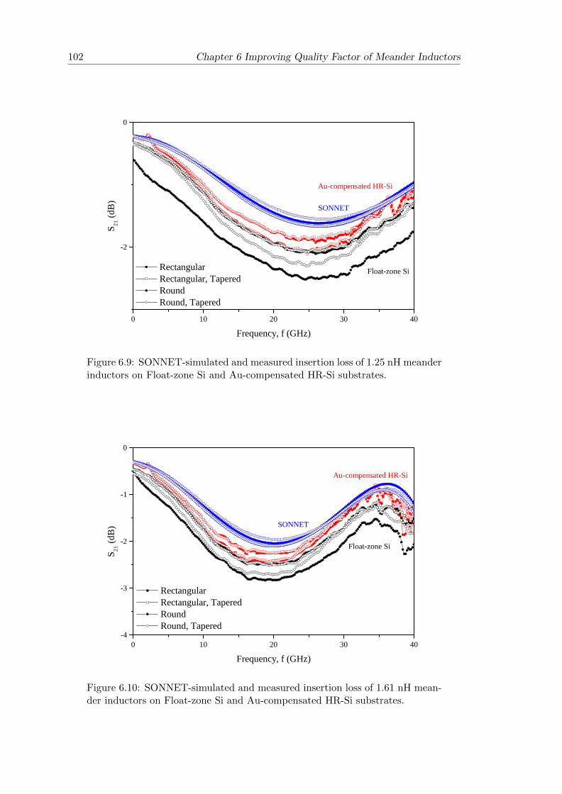
102 Chapter 6 Improving Quality Factor of Meander Inductors
0 1 0 2 0 3 0 4 0
- 2
0
S O N N E T
F l o a t - z o n e S i
A u - c o m p e n s a t e d H R - S i
S 21 (dB
)
F r e q u e n c y , f ( G H z )
R e c t a n g u l a r R e c t a n g u l a r , T a p e r e d R o u n d R o u n d , T a p e r e d
Figure 6.9: SONNET-simulated and measured insertion loss of 1.25 nH meanderinductors on Float-zone Si and Au-compensated HR-Si substrates.
0 1 0 2 0 3 0 4 0- 4
- 3
- 2
- 1
0
S O N N E T
F l o a t - z o n e S i
A u - c o m p e n s a t e d H R - S i
S 21 (dB
)
F r e q u e n c y , f ( G H z )
R e c t a n g u l a r R e c t a n g u l a r , T a p e r e d R o u n d R o u n d , T a p e r e d
Figure 6.10: SONNET-simulated and measured insertion loss of 1.61 nH mean-der inductors on Float-zone Si and Au-compensated HR-Si substrates.
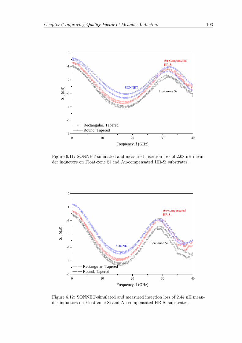
Chapter 6 Improving Quality Factor of Meander Inductors 103
0 1 0 2 0 3 0 4 0- 6
- 5
- 4
- 3
- 2
- 1
0
S O N N E TF l o a t - z o n e S i
A u - c o m p e n s a t e d H R - S i
S 21 (dB
)
F r e q u e n c y , f ( G H z )
R e c t a n g u l a r , T a p e r e d R o u n d , T a p e r e d
Figure 6.11: SONNET-simulated and measured insertion loss of 2.08 nH mean-der inductors on Float-zone Si and Au-compensated HR-Si substrates.
0 1 0 2 0 3 0 4 0
0 1 0 2 0 3 0 4 0
- 6
- 5
- 4
- 3
- 2
- 1
0
- 6
- 5
- 4
- 3
- 2
- 1
0
S 21 (dB
)
S O N N E T F l o a t - z o n e S i
A u - c o m p e n s a t e d H R - S i
F r e q u e n c y , f ( G H z )
R e c t a n g u l a r , T a p e r e d R o u n d , T a p e r e d
Figure 6.12: SONNET-simulated and measured insertion loss of 2.44 nH mean-der inductors on Float-zone Si and Au-compensated HR-Si substrates.
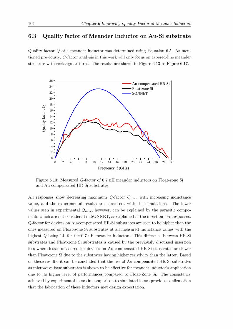
104 Chapter 6 Improving Quality Factor of Meander Inductors
6.3 Quality factor of Meander Inductor on Au-Si substrate
Quality factor Q of a meander inductor was determined using Equation 6.5. As men-
tioned previously, Q-factor analysis in this work will only focus on tapered-line meander
structure with rectangular turns. The results are shown in Figure 6.13 to Figure 6.17.
0 2 4 6 8 1 0 1 2 1 4 1 6 1 8 2 0 2 2 2 4 2 6 2 8 3 002468
1 01 21 41 61 82 02 22 42 6
Qualit
y fact
or, Q
F r e q u e n c y , f ( G H z )
A u - c o m p e n s a t e d H R - S i F l o a t - z o n e S i S O N N E T
Figure 6.13: Measured Q-factor of 0.7 nH meander inductors on Float-zone Siand Au-compensated HR-Si substrates.
All responses show decreasing maximum Q-factor Qmax with increasing inductance
value, and the experimental results are consistent with the simulations. The lower
values seen in experimental Qmax, however, can be explained by the parasitic compo-
nents which are not considered in SONNET, as explained in the insertion loss responses.
Q-factor for devices on Au-compensated HR-Si substrates are seen to be higher than the
ones measured on Float-zone Si substrates at all measured inductance values with the
highest Q being 14, for the 0.7 nH meander inductors. This difference between HR-Si
substrates and Float-zone Si substrates is caused by the previously discussed insertion
loss where losses measured for devices on Au-compensated HR-Si substrates are lower
than Float-zone Si due to the substrates having higher resistivity than the latter. Based
on these results, it can be concluded that the use of Au-compensated HR-Si substrates
as microwave base substrates is shown to be effective for meander inductor’s application
due to its higher level of performances compared to Float-Zone Si. The consistency
achieved by experimental losses in comparison to simulated losses provides confirmation
that the fabrication of these inductors met design expectation.
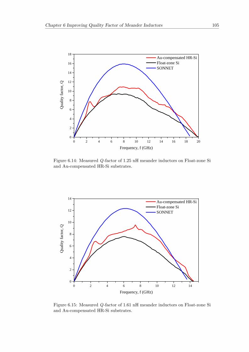
Chapter 6 Improving Quality Factor of Meander Inductors 105
0 2 4 6 8 1 0 1 2 1 4 1 6 1 8 2 00
2
4
6
8
1 0
1 2
1 4
1 6
1 8Qu
ality f
actor,
Q
F r e q u e n c y , f ( G H z )
A u - c o m p e n s a t e d H R - S i F l o a t - z o n e S i S O N N E T
Figure 6.14: Measured Q-factor of 1.25 nH meander inductors on Float-zone Siand Au-compensated HR-Si substrates.
0 2 4 6 8 1 0 1 2 1 40
2
4
6
8
1 0
1 2
1 4
Qualit
y fact
or, Q
F r e q u e n c y , f ( G H z )
A u - c o m p e n s a t e d H R - S i F l o a t - z o n e S i S O N N E T
Figure 6.15: Measured Q-factor of 1.61 nH meander inductors on Float-zone Siand Au-compensated HR-Si substrates.
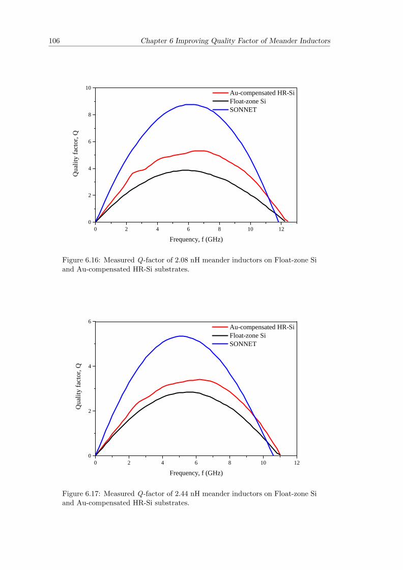
106 Chapter 6 Improving Quality Factor of Meander Inductors
0 2 4 6 8 1 0 1 20
2
4
6
8
1 0Qu
ality f
actor,
Q
F r e q u e n c y , f ( G H z )
A u - c o m p e n s a t e d H R - S i F l o a t - z o n e S i S O N N E T
Figure 6.16: Measured Q-factor of 2.08 nH meander inductors on Float-zone Siand Au-compensated HR-Si substrates.
0 2 4 6 8 1 0 1 20
2
4
6
Qualit
y fact
or, Q
F r e q u e n c y , f ( G H z )
A u - c o m p e n s a t e d H R - S i F l o a t - z o n e S i S O N N E T
Figure 6.17: Measured Q-factor of 2.44 nH meander inductors on Float-zone Siand Au-compensated HR-Si substrates.
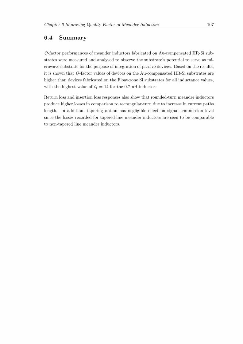
Chapter 6 Improving Quality Factor of Meander Inductors 107
6.4 Summary
Q-factor performances of meander inductors fabricated on Au-compensated HR-Si sub-
strates were measured and analysed to observe the substrate’s potential to serve as mi-
crowave substrate for the purpose of integration of passive devices. Based on the results,
it is shown that Q-factor values of devices on the Au-compensated HR-Si substrates are
higher than devices fabricated on the Float-zone Si substrates for all inductance values,
with the highest value of Q = 14 for the 0.7 nH inductor.
Return loss and insertion loss responses also show that rounded-turn meander inductors
produce higher losses in comparison to rectangular-turn due to increase in current paths
length. In addition, tapering option has negligible effect on signal tranmission level
since the losses recorded for tapered-line meander inductors are seen to be comparable
to non-tapered line meander inductors.

Chapter 7
Summary & Outlook
7.1 Summary
High resistivity substrates are desirable in microwave application to provide low loss
performance. In order to create high resistivity substrates, low concentration level of
background free carriers needs to be achieved. In this thesis, a high resistivity substrate is
developed through a concept called deep-level doping compensation, where background
free carriers in Si are compensated by elemental Au.
The concept consists of Au atoms compensating for the carriers by providing deep levels
near Si mid band gap and trapping them from freely conducting in the conduction band.
For optimum compensation, Au atoms are introduced into Si using ion-implantation
technique and activated via high temperature annealing procedure. The diffusion pro-
cess occurs through ’kick-out’ mechanism, by which a Au atom kicks out Si atom from
its lattice configuration and occupies the substitutional position inside Si lattice. For
optimum compensation, Au atoms are introduced into Si using ion-implantation tech-
nique and activated via high temperature annealing procedure. In this work, a gold dose
of 4 x 1013 cm−2 were injected through the backside of Czochralski-silicon substrates
with nominal resistivity of 50 Ω-cm. The implanted substrates were then annealed at
950 C in an Argon environment to activate the Au dopants. As a result, the substrate
resistivity was successfully enhanced to as high as 80 kΩ-cm, with an average value of
60 kΩ-cm for optimised implanted substrates.
Upon application at high frequency range, high resistivity silicon substrates suffer from
parasitic surface conduction, an effect that is bias-dependent, and occurs primarily due
to carriers near the Si surface during accumulation and inversion. The accumulation
and inversion of charges at the silicon surface creates a low resistivity surface region
which consequently increases substrate losses. This defeats the purpose of creating high
resistivity Si in the first place.
109
110 Chapter 7 Summary & Outlook
To address this issue, Au-compensated high resistivity silicon substrates developed in
this work are studied for its potential suppression of parasitic surface conduction using
deep-level doping compensation method. Metal-oxide-semiconductor (MOS) capacitors
are fabricated on Au-compensated HR-Si substrates to study the surface charge effect
associated with high resistivity substrates at the Si-SiO2 interface. Capacitance-voltage
characteristics of the devices show non-typical high frequency behaviour, with accumula-
tion capacitance significantly less than the oxide capacitance. The smaller accumulation
capacitance seen in the measurements is caused by the reduction of majority free carriers
and the correspondingly longer Debye length in high resistivity substrates. Comparing
the experimental results with the simulation results, capacitance obtained from experi-
ments are observed to be lower in all regions, indicating the potential of the substrate
to suppress the surface charge effect.
Microwave characterisations were used as a tool to evaluate the parasitic surface con-
duction effect on high resistivity silicon substrates under DC bias influence. Coplanar
waveguides were fabricated to observe the attenuation characteristics of the devices on
Au-compensated high resistivity silicon substrates. Under zero bias condition, the mea-
sured attenuations of CPWs on oxidised substrates are comparable to the attenuations
of CPWs on naked substrates, and are very much lower than the ones on oxidised Float-
zone Si substrates. These observations show the initial potential of parasitic surface
conduction suppression, with a recorded low attenuation of 0.19 dB/mm at 20 GHz.
Full suppression of the effect is successfully observed through microwave characterisa-
tions under DC bias influence. Unlike the bias-dependent attenuation values seen for
CPWs on 360 Ω-cm and 10 kΩ-cm Float-zone Si substrates, a constant attenuation value
of 0.19 dB/mm at 20 GHz is achieved throughout the whole range of bias voltage for
CPWs on Au-compensated high resistivity silicon substrates.
To reach this successful result, several process innovations have been designed and
achieved. One of the key innovations is the optimisation of the activation anneal-
ing procedure. Three different annealing treatment conditions were introduced; slow-
cooling, quenching and the combined procedure of slow-cooling and quenching. Slow-
cooling alone leads to very limited compensation. The highest resistivity enhancement
is achieved for substrates developed through the combined procedure. In terms of mi-
crowave device characteristics, CPWs fabricated on substrates developed through the
combined procedure show full suppression of parasitic surface conduction with measured
αmax/αmin ratio of 1 whereas CPWs fabricated on substrates developed through the sin-
gle quenching procedure show a slight attenuation-dependency with αmax/αmin ratio of
1.19. Based on these observations, the activation annealing is best conducted through
the combined procedure of slow-cooling and quenching to provide optimum resistivity
enhancement and low loss microwave characteristics.
Another essential point is the significance of the Au surface layer. Removing this Au
layer at the silicon surface by wet-etching helps to increase substrate resistivity. The
Chapter 7 Summary & Outlook 111
resistivity is increased to almost double the values before Au-etching. However, from
a microwave point of view, full suppression of parasitic surface conduction is seen in
both cases, with and without Au-etching. Actually, the attenuation losses of CPWs
fabricated on substrates without Au layer removal are lower than the ones on substrates
with Au layer removal, indicating that the existence of a Au layer at the silicon surface
provides additional benefits. Therefore, the Au surface removal through wet-etching is
not required to improve microwave performance, leading to reduced complexity in the
fabrication process.
The type of oxide used as the passivation layer also has an important role in suppress-
ing parasitic surface conduction using Au-compensated high resistivity silicon substrate.
The effect is fully suppressed on substrates with sputtered oxide with αmax/αmin ratio of
1, whereas a strong bias-dependent attenuation characteristic is seen on substrates with
thermal oxide, with a recorded αmax/αmin ratio of 1.70. The increase in attenuation
and its bias-dependent characteristics for the latter oxide are contributed to the high
processing temperature during oxidation, which lowers the substitutional Au concentra-
tion.
Having presented the points above, suppression of parasitic surface conduction in bulk
high resistivity silicon can be achieved via deep-level doping compensation technique.
The highest level of microwave performance is observed for non Au-etched, Au-compensated
high resistivity silicon substrate developed through the combined annealing procedure
of slow-cooling and quenching with sputtered oxide. The best value is 0.19 dB/mm at
20 GHz and is constant throughout the whole range of voltage measured, indicating
full suppression of the effect. Microwave performance of meander inductors fabricated
on these Au-compensated high resistivity silicon substrates were evaluated to further
indicate the potential of the substrate. The quality factor of these inductors are higher
than those fabricated on Float-zone silicon substrates. The best value of Q-factor is 14,
for a 0.7-nH inductor.
In conclusion, increased performance of microwave devices fabricated on Au-compensated
high resistivity silicon provides a clear demonstration of the effectiveness of the deep-
level doping compensation method in providing an alternative to the currently available
microwave substrates, offering reduced fabrication complexity and lower manufacturing
cost.
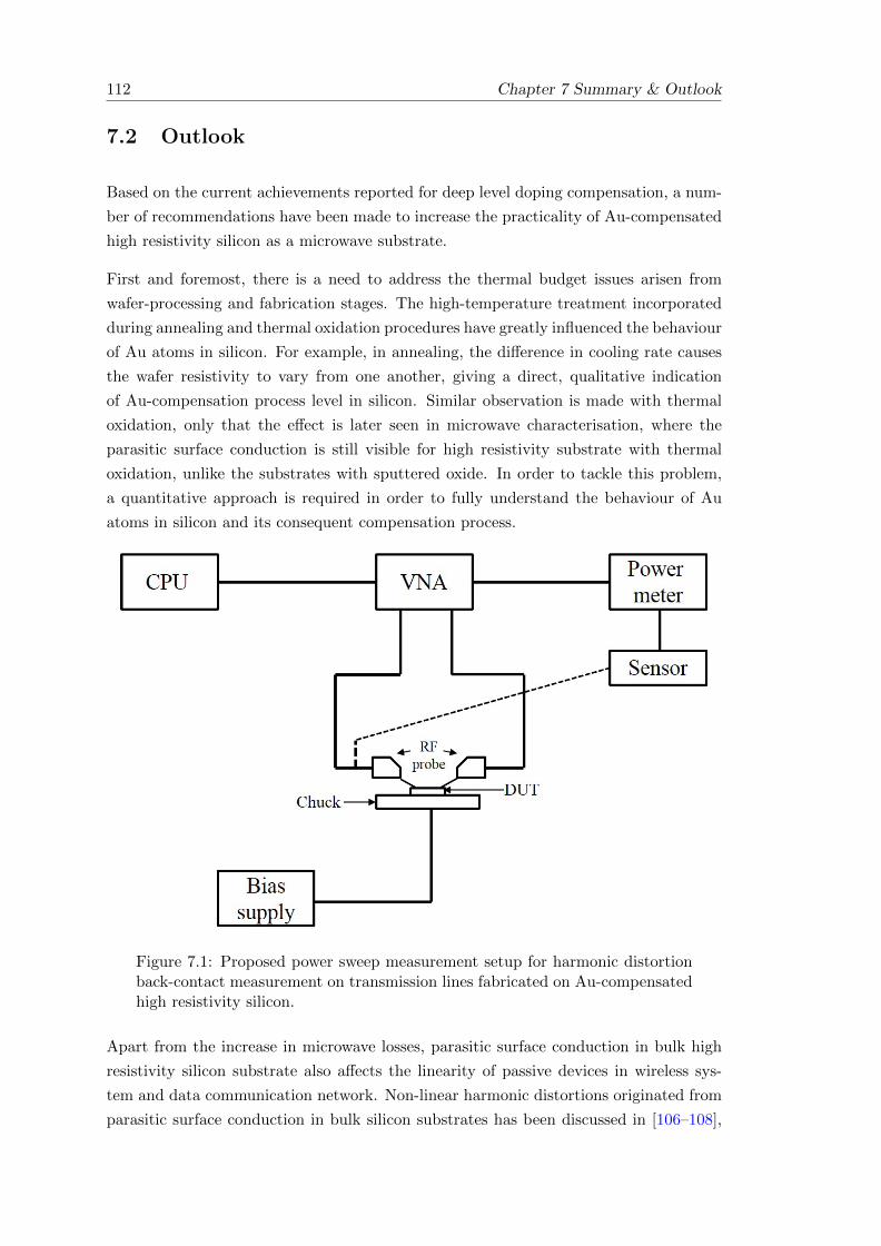
112 Chapter 7 Summary & Outlook
7.2 Outlook
Based on the current achievements reported for deep level doping compensation, a num-
ber of recommendations have been made to increase the practicality of Au-compensated
high resistivity silicon as a microwave substrate.
First and foremost, there is a need to address the thermal budget issues arisen from
wafer-processing and fabrication stages. The high-temperature treatment incorporated
during annealing and thermal oxidation procedures have greatly influenced the behaviour
of Au atoms in silicon. For example, in annealing, the difference in cooling rate causes
the wafer resistivity to vary from one another, giving a direct, qualitative indication
of Au-compensation process level in silicon. Similar observation is made with thermal
oxidation, only that the effect is later seen in microwave characterisation, where the
parasitic surface conduction is still visible for high resistivity substrate with thermal
oxidation, unlike the substrates with sputtered oxide. In order to tackle this problem,
a quantitative approach is required in order to fully understand the behaviour of Au
atoms in silicon and its consequent compensation process.
Figure 7.1: Proposed power sweep measurement setup for harmonic distortionback-contact measurement on transmission lines fabricated on Au-compensatedhigh resistivity silicon.
Apart from the increase in microwave losses, parasitic surface conduction in bulk high
resistivity silicon substrate also affects the linearity of passive devices in wireless sys-
tem and data communication network. Non-linear harmonic distortions originated from
parasitic surface conduction in bulk silicon substrates has been discussed in [106–108],
Chapter 7 Summary & Outlook 113
where its occurrence is said to be detrimental to the system, if the power level is higher
than the ones in other microwave circuitries and active components. It is therefore im-
portant to observe this non-linear behaviour in Au-compensated high resistivity silicon
to ensure full suppression of parasitic surface conduction is by all means, achieved. Kerr
et al. proposed the power sweep measurement setup used to measure second and third
harmonic distortion level of transmission line fabricated on passivated bulk high resis-
tivity silicon [109]. However, the setup can be altered to employ the back metallisation
of the microwave structure in this work. The proposed setup for measurement using
back contact is as shown in Figure 7.1.
The proposed work can then be utilised to form the solid basis of fully incorporating this
substrate into microwave applications such as integrated passive devices and through-
silicon-vias for 3D-integration.

References
[1] T. Lee, “CMOS RF: No longer an oxymoron,” in Gallium Arsenide Integrated
Circuit (GaAs IC) Symposium, 1997. Technical Digest 1997., 19th Annual, 1997,
pp. 244–247.
[2] T. Instruments. (2005) ISM-band and short range device regulatory compliance
overview. [Online]. Available: http://www.ti.com/lit/an/swra048/swra048.pdf
[3] D. Leipold, W. Schwartz, and K.-H. Kraus, “Integrated CMOS circuit for use
at high frequencies,” Patent US 6 348 718, Feb 19, 2002. [Online]. Available:
http://www.google.com/patents/US6348718
[4] J.-P. Raskin, A. Viviani, D. Flandre, and J. Colinge, “Substrate crosstalk reduction
using SOI technology,” Electron Devices, IEEE Transactions on, vol. 44, no. 12,
pp. 2252–2261, 1997.
[5] A. Niknejad and R. Meyer, “Analysis of eddy-current losses over conductive sub-
strates with applications to monolithic inductors and transformers,” Microwave
Theory and Techniques, IEEE Transactions on, vol. 49, no. 1, pp. 166–176, 2001.
[6] J. Yang, K. Benaissa, D. Crenshaw, B. Williams, S. Sridhar, J. Ai, G. Boselli,
S. Zhao, S.-P. Tang, N. Mahalingam, S. Ashburn, P. Madhani, T. Blythe, and
H. Shichijo, “0.1 µm RFCMOS on high resistivity substrates for system on chip
(SOC) applications,” in Electron Devices Meeting, 2002. IEDM ’02. International,
2002, pp. 667–670.
[7] E. Mehal and R. Wacker, “GaAs integrated microwave circuits,” Microwave The-
ory and Techniques, IEEE Transactions on, vol. 16, no. 7, pp. 451–454, Jul 1968.
[8] R. Dekker, P. Baltus, M. van Deurzen, W. Einden, H. Maas, and A. Wagemans,
“An ultra low-power RF bipolar technology on glass,” in Electron Devices Meeting,
1997. IEDM ’97. Technical Digest., International, Dec 1997, pp. 921–923.
[9] R. Dekker, P. Baltus, and H. Maas, “Substrate transfer for radio frequency tech-
nologies,” Electron Devices, IEEE Transactions on, vol. 50, no. 3, pp. 747–757,
2003.
115
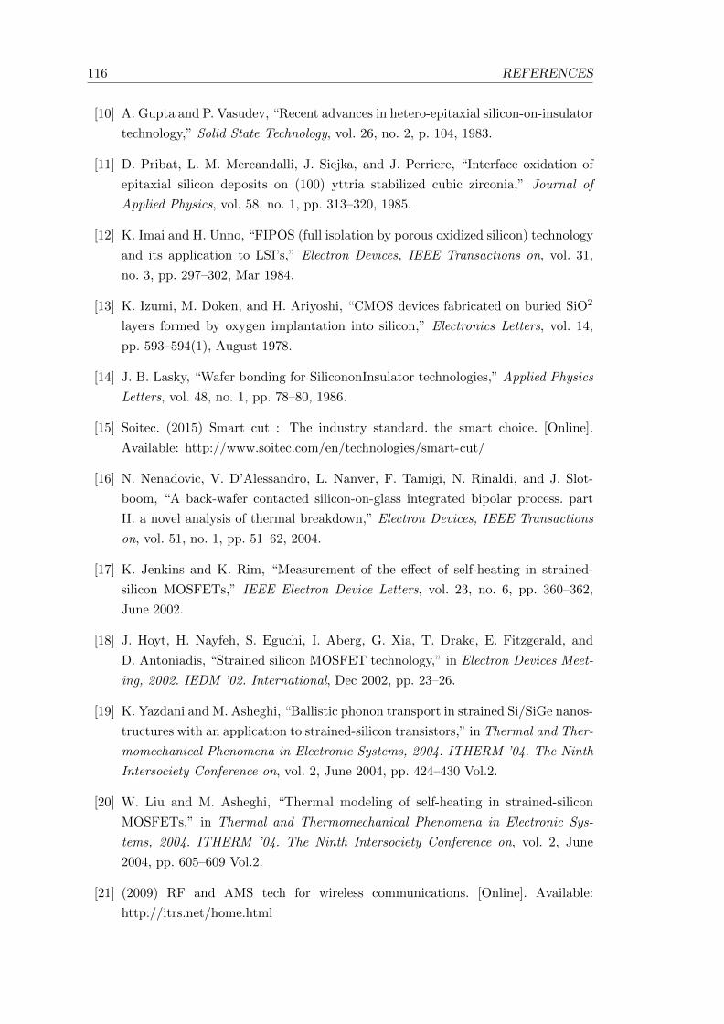
116 REFERENCES
[10] A. Gupta and P. Vasudev, “Recent advances in hetero-epitaxial silicon-on-insulator
technology,” Solid State Technology, vol. 26, no. 2, p. 104, 1983.
[11] D. Pribat, L. M. Mercandalli, J. Siejka, and J. Perriere, “Interface oxidation of
epitaxial silicon deposits on (100) yttria stabilized cubic zirconia,” Journal of
Applied Physics, vol. 58, no. 1, pp. 313–320, 1985.
[12] K. Imai and H. Unno, “FIPOS (full isolation by porous oxidized silicon) technology
and its application to LSI’s,” Electron Devices, IEEE Transactions on, vol. 31,
no. 3, pp. 297–302, Mar 1984.
[13] K. Izumi, M. Doken, and H. Ariyoshi, “CMOS devices fabricated on buried SiO2
layers formed by oxygen implantation into silicon,” Electronics Letters, vol. 14,
pp. 593–594(1), August 1978.
[14] J. B. Lasky, “Wafer bonding for SilicononInsulator technologies,” Applied Physics
Letters, vol. 48, no. 1, pp. 78–80, 1986.
[15] Soitec. (2015) Smart cut : The industry standard. the smart choice. [Online].
Available: http://www.soitec.com/en/technologies/smart-cut/
[16] N. Nenadovic, V. D’Alessandro, L. Nanver, F. Tamigi, N. Rinaldi, and J. Slot-
boom, “A back-wafer contacted silicon-on-glass integrated bipolar process. part
II. a novel analysis of thermal breakdown,” Electron Devices, IEEE Transactions
on, vol. 51, no. 1, pp. 51–62, 2004.
[17] K. Jenkins and K. Rim, “Measurement of the effect of self-heating in strained-
silicon MOSFETs,” IEEE Electron Device Letters, vol. 23, no. 6, pp. 360–362,
June 2002.
[18] J. Hoyt, H. Nayfeh, S. Eguchi, I. Aberg, G. Xia, T. Drake, E. Fitzgerald, and
D. Antoniadis, “Strained silicon MOSFET technology,” in Electron Devices Meet-
ing, 2002. IEDM ’02. International, Dec 2002, pp. 23–26.
[19] K. Yazdani and M. Asheghi, “Ballistic phonon transport in strained Si/SiGe nanos-
tructures with an application to strained-silicon transistors,” in Thermal and Ther-
momechanical Phenomena in Electronic Systems, 2004. ITHERM ’04. The Ninth
Intersociety Conference on, vol. 2, June 2004, pp. 424–430 Vol.2.
[20] W. Liu and M. Asheghi, “Thermal modeling of self-heating in strained-silicon
MOSFETs,” in Thermal and Thermomechanical Phenomena in Electronic Sys-
tems, 2004. ITHERM ’04. The Ninth Intersociety Conference on, vol. 2, June
2004, pp. 605–609 Vol.2.
[21] (2009) RF and AMS tech for wireless communications. [Online]. Available:
http://itrs.net/home.html
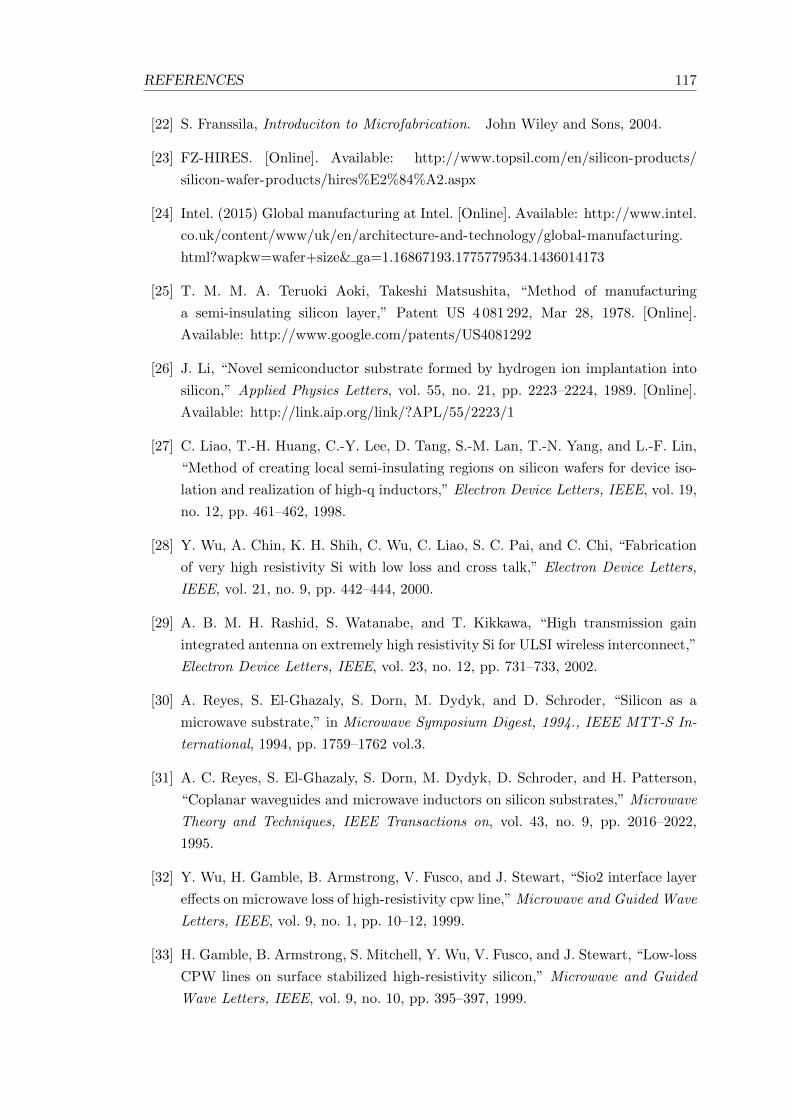
REFERENCES 117
[22] S. Franssila, Introduciton to Microfabrication. John Wiley and Sons, 2004.
[23] FZ-HIRES. [Online]. Available: http://www.topsil.com/en/silicon-products/
silicon-wafer-products/hires%E2%84%A2.aspx
[24] Intel. (2015) Global manufacturing at Intel. [Online]. Available: http://www.intel.
co.uk/content/www/uk/en/architecture-and-technology/global-manufacturing.
html?wapkw=wafer+size& ga=1.16867193.1775779534.1436014173
[25] T. M. M. A. Teruoki Aoki, Takeshi Matsushita, “Method of manufacturing
a semi-insulating silicon layer,” Patent US 4 081 292, Mar 28, 1978. [Online].
Available: http://www.google.com/patents/US4081292
[26] J. Li, “Novel semiconductor substrate formed by hydrogen ion implantation into
silicon,” Applied Physics Letters, vol. 55, no. 21, pp. 2223–2224, 1989. [Online].
Available: http://link.aip.org/link/?APL/55/2223/1
[27] C. Liao, T.-H. Huang, C.-Y. Lee, D. Tang, S.-M. Lan, T.-N. Yang, and L.-F. Lin,
“Method of creating local semi-insulating regions on silicon wafers for device iso-
lation and realization of high-q inductors,” Electron Device Letters, IEEE, vol. 19,
no. 12, pp. 461–462, 1998.
[28] Y. Wu, A. Chin, K. H. Shih, C. Wu, C. Liao, S. C. Pai, and C. Chi, “Fabrication
of very high resistivity Si with low loss and cross talk,” Electron Device Letters,
IEEE, vol. 21, no. 9, pp. 442–444, 2000.
[29] A. B. M. H. Rashid, S. Watanabe, and T. Kikkawa, “High transmission gain
integrated antenna on extremely high resistivity Si for ULSI wireless interconnect,”
Electron Device Letters, IEEE, vol. 23, no. 12, pp. 731–733, 2002.
[30] A. Reyes, S. El-Ghazaly, S. Dorn, M. Dydyk, and D. Schroder, “Silicon as a
microwave substrate,” in Microwave Symposium Digest, 1994., IEEE MTT-S In-
ternational, 1994, pp. 1759–1762 vol.3.
[31] A. C. Reyes, S. El-Ghazaly, S. Dorn, M. Dydyk, D. Schroder, and H. Patterson,
“Coplanar waveguides and microwave inductors on silicon substrates,” Microwave
Theory and Techniques, IEEE Transactions on, vol. 43, no. 9, pp. 2016–2022,
1995.
[32] Y. Wu, H. Gamble, B. Armstrong, V. Fusco, and J. Stewart, “Sio2 interface layer
effects on microwave loss of high-resistivity cpw line,” Microwave and Guided Wave
Letters, IEEE, vol. 9, no. 1, pp. 10–12, 1999.
[33] H. Gamble, B. Armstrong, S. Mitchell, Y. Wu, V. Fusco, and J. Stewart, “Low-loss
CPW lines on surface stabilized high-resistivity silicon,” Microwave and Guided
Wave Letters, IEEE, vol. 9, no. 10, pp. 395–397, 1999.
118 REFERENCES
[34] H.-T. Lue, T.-Y. Tseng, and G.-W. Huang, “A method to characterize the di-
electric and interfacial properties of metalinsulator-semiconductor structures by
microwave measurement,” Journal of Applied Physics, vol. 91, no. 8, 2002.
[35] D. Lederer and J.-P. Raskin, “Effective resistivity of fully-processed SOI sub-
strates,” Solid-State Electronics, vol. 49, no. 3, pp. 491 – 496, 2005.
[36] A. Jansman, J. Van Beek, M. Van Delden, A. L. A. M. Kemmeren, A. Den Dekker,
and F. Widdershoven, “Elimination of accumulation charge effects for high-
resistive silicon substrates,” in European Solid-State Device Research, 2003. ESS-
DERC ’03. 33rd Conference on, 2003, pp. 3–6.
[37] E. Valletta, J. Van Beek, A. Den Dekker, N. Pulsford, H. F. F. Jos, L. de Vreede,
L. Nanver, and J. Burghartz, “Design and characterization of integrated passive
elements on high ohmic silicon,” in Microwave Symposium Digest, 2003 IEEE
MTT-S International, vol. 2, 2003, pp. 1235–1238.
[38] M. Spirito, F. De Paola, L. Nanver, E. Valletta, B. Rong, B. Rejaei, L. de Vreede,
and J. Burghartz, “Surface-passivated high-resistivity silicon as a true microwave
substrate,” Microwave Theory and Techniques, IEEE Transactions on, vol. 53,
no. 7, pp. 2340–2347, 2005.
[39] H. Li, R. Franken, R. Stolk, C. van der Werf, J. Rath, and R. Schropp, “Control-
ling the quality of nanocrystalline silicon made by hot-wire chemical vapor deposi-
tion by using a reverse hydrogen profiling technique,” Journal of Non-Crystalline
Solids, vol. 354, pp. 2087 – 2091, 2008.
[40] C.-J. Chen, R.-L. Wang, Y.-K. Su, and T.-J. Hsueh, “A nanocrystalline silicon
surface-passivation layer on an HR-Si substrate for RFICs,” Electron Device Let-
ters, IEEE, vol. 32, no. 3, pp. 369–371, 2011.
[41] R.-L. Wang, Y.-K. Su, C.-J. Chen, and T.-J. Hsueh, “Nanocrystalline silicon thick-
ness dependence of transmission characteristics of CPWs on surface-passivated
highresistivity silicon substrates,” Electronics Letters, vol. 47, no. 20, pp. 1133–
1134, 2011.
[42] K. Misiakos and D. Tsamakis, “Accurate measurements of the silicon intrinsic
carrier density from 78 to 340 K,” Journal of Applied Physics, vol. 74, no. 5,
pp. 3293–3297, 1993. [Online]. Available: http://scitation.aip.org/content/aip/
journal/jap/74/5/10.1063/1.354551
[43] W. Schroter and M. Seibt, Properties of Crystalline Silicon: Deep Levels of Tran-
sition Metal Impurities in c-Si. R. Hull (Editor), The Institution of Electrical
Engineers, London, 1999.
REFERENCES 119
[44] K. Mallik, R. J. Falster, and P. R. Wilshaw, “’Semi-insulating’ silicon
using deep level impurity doping: problems and potential,” Semiconductor
Science and Technology, vol. 18, no. 6, p. 517, 2003. [Online]. Available:
http://stacks.iop.org/0268-1242/18/i=6/a=321
[45] A. Milnes, Deep Impurities in Silicon. John Wiley and Sons, 1973.
[46] S. Sze, Semiconductor Devices: Physics and Technology. New York:John Wiley
and Sons, 1936, ch. Carrier Concentration at Thermal Equilibrium, p. 19.
[47] R. Wang, S. Campell, R. Tan, J. Meyer, and Y. Cai, “Semi-insulating silicon
substrates for silicon based RF integrated circuits,” in Silicon Monolithic Integrated
Circuits in RF Systems, 1998. Digest of Papers. 1998 Topical Meeting on, 1998,
pp. 164–168.
[48] D. M. Jordan, R. H. Haslam, K. Mallik, R. J. Falster, and P. R. Wilshaw, “The
development of semi-insulating silicon substrates for microwave devices,” Journal
of The Electrochemical Society, vol. 157, no. 5, pp. H540–H545, 2010. [Online].
Available: http://jes.ecsdl.org/content/157/5/H540.abstract
[49] G. A. Adegboyega, L. Passari, M. A. Butturi, A. Poggi, and E. Suzi, “Electri-
cal Properties of Silver Impurities and their Annealing Behaviour in p-Type Fz
Silicon,” Journal de Physique III, vol. 6, pp. 1691–1696, Dec. 1996.
[50] H. Kitagawa, “Diffusion and electrical properties of 3D transition-metal impurities
in Silicon,” Solid State Phenomena, vol. 71, pp. 51–72, 2000.
[51] C. B. Collins, R. O. Carlson, and C. J. Gallagher, “Properties of gold-doped
silicon,” Phys. Rev., vol. 105, pp. 1168–1173, Feb 1957. [Online]. Available:
http://link.aps.org/doi/10.1103/PhysRev.105.1168
[52] G. Bemski, “Recombination properties of gold in silicon,” Phys. Rev., vol. 111,
pp. 1515–1518, Sep 1958. [Online]. Available: http://link.aps.org/doi/10.1103/
PhysRev.111.1515
[53] G. A. Adegboyega, O. Osasona, and E. Susi, “Intrinsic gettering of manganese
impurity in silicon substrate,” physica status solidi (a), vol. 161, no. 1, pp. 231–
235, 1997. [Online]. Available: http://dx.doi.org/10.1002/1521-396X(199705)161:
1〈231::AID-PSSA231〉3.0.CO;2-I
[54] W. Bullis, “Properties of gold in silicon,” Solid-State Electronics, vol. 9, no. 2,
pp. 143 – 168, 1966. [Online]. Available: http://www.sciencedirect.com/science/
article/pii/0038110166900852
[55] W. R. Wilcox, T. J. LaChapelle, and D. H. Forbes, “Gold in silicon: Effect on
resistivity and diffusion in heavily-doped layers,” Journal of The Electrochemical
Society, vol. 111, no. 12, pp. 1377–1380, 1964.
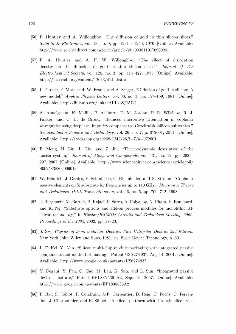
120 REFERENCES
[56] F. Huntley and A. Willoughby, “The diffusion of gold in thin silicon slices,”
Solid-State Electronics, vol. 13, no. 9, pp. 1231 – 1240, 1970. [Online]. Available:
http://www.sciencedirect.com/science/article/pii/0038110170900201
[57] F. A. Huntley and A. F. W. Willoughby, “The effect of dislocation
density on the diffusion of gold in thin silicon slices,” Journal of The
Electrochemical Society, vol. 120, no. 3, pp. 414–422, 1973. [Online]. Available:
http://jes.ecsdl.org/content/120/3/414.abstract
[58] U. Gosele, F. Morehead, W. Frank, and A. Seeger, “Diffusion of gold in silicon: A
new model,” Applied Physics Letters, vol. 38, no. 3, pp. 157–159, 1981. [Online].
Available: http://link.aip.org/link/?APL/38/157/1
[59] A. Abuelgasim, K. Mallik, P. Ashburn, D. M. Jordan, P. R. Wilshaw, R. J.
Falster, and C. H. de Groot, “Reduced microwave attenuation in coplanar
waveguides using deep level impurity compensated Czochralski-silicon substrates,”
Semiconductor Science and Technology, vol. 26, no. 7, p. 072001, 2011. [Online].
Available: http://stacks.iop.org/0268-1242/26/i=7/a=072001
[60] F. Meng, H. Liu, L. Liu, and Z. Jin, “Thermodynamic description of the
ausisn system,” Journal of Alloys and Compounds, vol. 431, no. 12, pp. 292 –
297, 2007. [Online]. Available: http://www.sciencedirect.com/science/article/pii/
S0925838806006013
[61] W. Heinrich, J. Gerdes, F. Schmiickle, C. Rheinfelder, and K. Strohm, “Coplanar
passive elements on Si substrate for frequencies up to 110 GHz,” Microwave Theory
and Techniques, IEEE Transactions on, vol. 46, no. 5, pp. 709–712, 1998.
[62] J. Burghartz, M. Bartek, B. Rejaei, P. Sarro, A. Polyakov, N. Pham, E. Boullaard,
and K. Ng, “Substrate options and add-on process modules for monolithic RF
silicon technology,” in Bipolar/BiCMOS Circuits and Technology Meeting, 2002.
Proceedings of the 2002, 2002, pp. 17–23.
[63] S. Sze, Physics of Semiconductor Devices, Part II:Bipolar Devices 2nd Edition.
New York:John Wiley and Sons, 1981, ch. Basic Device Technology, p. 69.
[64] L. F. Kei. Y. Ahn, “Silicon multi-chip module packaging with integrated passive
components and method of making,” Patent US6 274 937, Aug 14, 2001. [Online].
Available: http://www.google.co.uk/patents/US6274937
[65] Y. Degani, Y. Fan, C. Gao, M. Lau, K. Sun, and L. Sun, “Integrated passive
device substrate,” Patent EP1 835 536 A2, Sept 19, 2007. [Online]. Available:
http://www.google.com/patents/EP1835536A2
[66] P. Bar, S. Joblot, P. Coudrain, J.-F. Carpentier, B. Reig, C. Fuchs, C. Ferran-
don, J. Charbonnier, and H. Sibuet, “A silicon platform with through-silicon vias
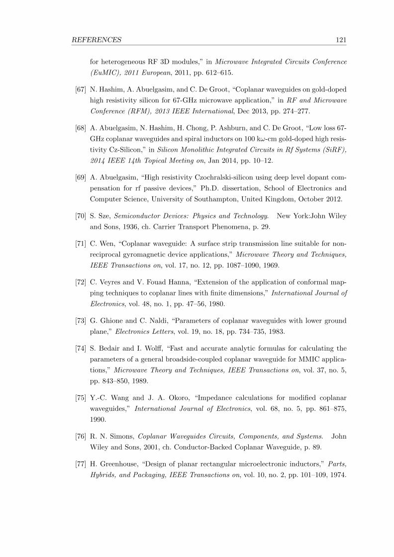
REFERENCES 121
for heterogeneous RF 3D modules,” in Microwave Integrated Circuits Conference
(EuMIC), 2011 European, 2011, pp. 612–615.
[67] N. Hashim, A. Abuelgasim, and C. De Groot, “Coplanar waveguides on gold-doped
high resistivity silicon for 67-GHz microwave application,” in RF and Microwave
Conference (RFM), 2013 IEEE International, Dec 2013, pp. 274–277.
[68] A. Abuelgasim, N. Hashim, H. Chong, P. Ashburn, and C. De Groot, “Low loss 67-
GHz coplanar waveguides and spiral inductors on 100 kω-cm gold-doped high resis-
tivity Cz-Silicon,” in Silicon Monolithic Integrated Circuits in Rf Systems (SiRF),
2014 IEEE 14th Topical Meeting on, Jan 2014, pp. 10–12.
[69] A. Abuelgasim, “High resistivity Czochralski-silicon using deep level dopant com-
pensation for rf passive devices,” Ph.D. dissertation, School of Electronics and
Computer Science, University of Southampton, United Kingdom, October 2012.
[70] S. Sze, Semiconductor Devices: Physics and Technology. New York:John Wiley
and Sons, 1936, ch. Carrier Transport Phenomena, p. 29.
[71] C. Wen, “Coplanar waveguide: A surface strip transmission line suitable for non-
reciprocal gyromagnetic device applications,” Microwave Theory and Techniques,
IEEE Transactions on, vol. 17, no. 12, pp. 1087–1090, 1969.
[72] C. Veyres and V. Fouad Hanna, “Extension of the application of conformal map-
ping techniques to coplanar lines with finite dimensions,” International Journal of
Electronics, vol. 48, no. 1, pp. 47–56, 1980.
[73] G. Ghione and C. Naldi, “Parameters of coplanar waveguides with lower ground
plane,” Electronics Letters, vol. 19, no. 18, pp. 734–735, 1983.
[74] S. Bedair and I. Wolff, “Fast and accurate analytic formulas for calculating the
parameters of a general broadside-coupled coplanar waveguide for MMIC applica-
tions,” Microwave Theory and Techniques, IEEE Transactions on, vol. 37, no. 5,
pp. 843–850, 1989.
[75] Y.-C. Wang and J. A. Okoro, “Impedance calculations for modified coplanar
waveguides,” International Journal of Electronics, vol. 68, no. 5, pp. 861–875,
1990.
[76] R. N. Simons, Coplanar Waveguides Circuits, Components, and Systems. John
Wiley and Sons, 2001, ch. Conductor-Backed Coplanar Waveguide, p. 89.
[77] H. Greenhouse, “Design of planar rectangular microelectronic inductors,” Parts,
Hybrids, and Packaging, IEEE Transactions on, vol. 10, no. 2, pp. 101–109, 1974.
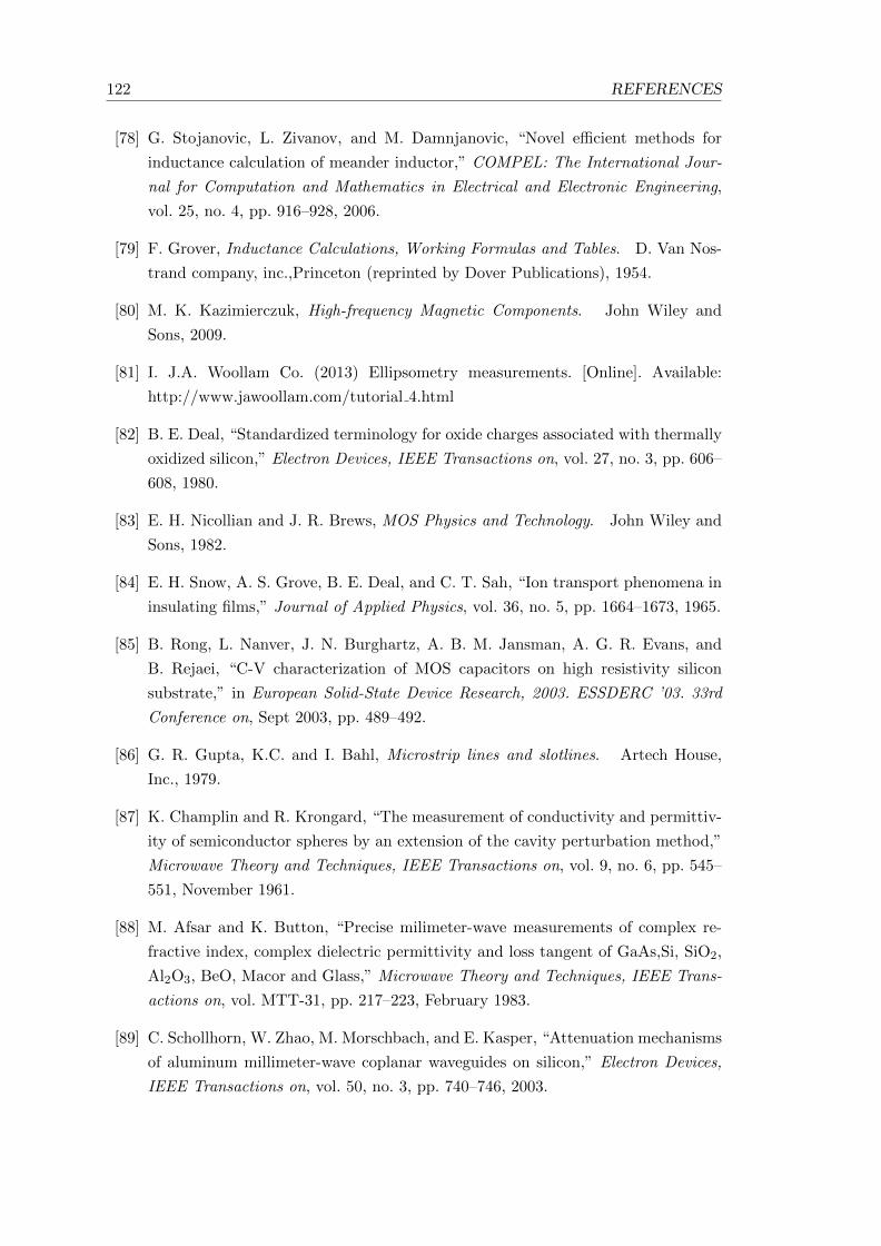
122 REFERENCES
[78] G. Stojanovic, L. Zivanov, and M. Damnjanovic, “Novel efficient methods for
inductance calculation of meander inductor,” COMPEL: The International Jour-
nal for Computation and Mathematics in Electrical and Electronic Engineering,
vol. 25, no. 4, pp. 916–928, 2006.
[79] F. Grover, Inductance Calculations, Working Formulas and Tables. D. Van Nos-
trand company, inc.,Princeton (reprinted by Dover Publications), 1954.
[80] M. K. Kazimierczuk, High-frequency Magnetic Components. John Wiley and
Sons, 2009.
[81] I. J.A. Woollam Co. (2013) Ellipsometry measurements. [Online]. Available:
http://www.jawoollam.com/tutorial 4.html
[82] B. E. Deal, “Standardized terminology for oxide charges associated with thermally
oxidized silicon,” Electron Devices, IEEE Transactions on, vol. 27, no. 3, pp. 606–
608, 1980.
[83] E. H. Nicollian and J. R. Brews, MOS Physics and Technology. John Wiley and
Sons, 1982.
[84] E. H. Snow, A. S. Grove, B. E. Deal, and C. T. Sah, “Ion transport phenomena in
insulating films,” Journal of Applied Physics, vol. 36, no. 5, pp. 1664–1673, 1965.
[85] B. Rong, L. Nanver, J. N. Burghartz, A. B. M. Jansman, A. G. R. Evans, and
B. Rejaei, “C-V characterization of MOS capacitors on high resistivity silicon
substrate,” in European Solid-State Device Research, 2003. ESSDERC ’03. 33rd
Conference on, Sept 2003, pp. 489–492.
[86] G. R. Gupta, K.C. and I. Bahl, Microstrip lines and slotlines. Artech House,
Inc., 1979.
[87] K. Champlin and R. Krongard, “The measurement of conductivity and permittiv-
ity of semiconductor spheres by an extension of the cavity perturbation method,”
Microwave Theory and Techniques, IEEE Transactions on, vol. 9, no. 6, pp. 545–
551, November 1961.
[88] M. Afsar and K. Button, “Precise milimeter-wave measurements of complex re-
fractive index, complex dielectric permittivity and loss tangent of GaAs,Si, SiO2,
Al2O3, BeO, Macor and Glass,” Microwave Theory and Techniques, IEEE Trans-
actions on, vol. MTT-31, pp. 217–223, February 1983.
[89] C. Schollhorn, W. Zhao, M. Morschbach, and E. Kasper, “Attenuation mechanisms
of aluminum millimeter-wave coplanar waveguides on silicon,” Electron Devices,
IEEE Transactions on, vol. 50, no. 3, pp. 740–746, 2003.
REFERENCES 123
[90] B. Rejaei, K. Ng, C. Floerkemeier, N. Pham, L. Nanver, and J. Burghartz, “In-
tegrated transmission lines on high-resistivity silicon: Coplanar waveguides or
microstrips?” in Solid-State Device Research Conference, 2000. Proceeding of the
30th European, 2000, pp. 460–463.
[91] D. Lederer and J.-P. Raskin, “Substrate loss mechanisms for microstrip and CPW
transmission lines on lossy silicon wafers,” Solid-State Electronics, vol. 47, pp.
1927–1936, 2003.
[92] D. Sarkar, Physical and Chemical Methods in Soil Analysis: Beer-Lambert’s Law.
New Age International, 2005.
[93] D. M. Pozar, Microwave Engineering. John Wiley and Sons, 2012, ch. Transmis-
sion line theory.
[94] R. B. Marks and D. F. Williams, “A general waveguide circuit theory,” Journal
of Research of the National Institute of Standards and Technology, vol. 97, pp.
533–561, 1992.
[95] Y. Eo and W. Eisenstadt, “High-speed VLSI interconnect modeling based on S-
parameter measurements,” Components, Hybrids, and Manufacturing Technology,
IEEE Transactions on, vol. 16, no. 5, pp. 555–562, Aug 1993.
[96] S. Evseev, L. Nanver, and S. Milosavljevic, “AlN thin-film deposition for sup-
pressing surface current losses in RF circuits on high-resistivity silicon,” in Bipo-
lar/BiCMOS Circuits and Technology Meeting (BCTM), 2013 IEEE, Sept 2013,
pp. 77–80.
[97] D. Lederer and J. P. Raskin, “New substrate passivation method dedicated to
HR SOI wafer fabrication with increased substrate resistivity,” Electron Device
Letters, IEEE, vol. 26, no. 11, pp. 805–807, Nov 2005.
[98] W. Kuhn, “Loss mechanisms and quality factor improvement for inductors in high-
resistivity SOI processes,” in Silicon Monolithic Integrated Circuits in RF Systems
(SiRF), 2012 IEEE 12th Topical Meeting on, Jan 2012, pp. 29–32.
[99] P. Sarafis, E. Hourdakis, A. Nassiopoulou, C. Neve, K. Ben Ali, and J.-P. Raskin,
“Advanced Si-based substrates for RF passive integration: Comparison between
local porous Si layer technology and trap-rich high resistivity Si,” Solid-State Elec-
tronics, vol. 87, pp. 27 – 33, 2013.
[100] J.-M. Yook, D. Kim, and J. C. Kim, “High-Q trenched spiral inductors and low-loss
low pass filters using through silicon via processes,” Japanese Journal of Applied
Physics, vol. 53, no. 4S, p. 04EE11, 2014.
[101] N. Li, K. Okada, T. Inoue, T. Hirano, Q. Bu, A. Narayanan, T. Siriburanon,
H. Sakane, and A. Matsuzawa, “High-Q inductors on locally semi-insulated Si
124 REFERENCES
substrate by Helium-3 bombardment for RF CMOS integrated circuits,” Electron
Devices, IEEE Transactions on, vol. 62, no. 4, pp. 1269–1275, April 2015.
[102] T. Lee, The Design of CMOS Radio-Frequency Integrated Circuits. Cam-
bridge:Cambridge University Press, 2004.
[103] D. M. Pozar, Microwave Engineering. John Wiley and Sons, 2012, ch. Microwave
network analysis.
[104] G. Radosavljevic, A. Maric, L. Zivanov, and W. Smetana, “Realization of high
quality RF inductors using LTCC technology,” in Telecommunications Forum
(TELFOR), 2011 19th, 2011, pp. 984–987.
[105] G. Vendelin, Design of Amplifiers and Oscillators by the S-parameter Method.
John WIley & Sons, 1982.
[106] A. Botula, A. Joseph, J. Slinkman, R. Wolf, Z.-X. He, D. Ioannou, L. Wagner,
M. Gordon, M. Abou-Khalil, R. Phelps, M. Gautsch, W. Abadeer, D. Harmon,
M. Levy, J. Benoit, and J. Dunn, “A thin-film soi 180nm cmos rf switch technol-
ogy,” in Silicon Monolithic Integrated Circuits in RF Systems, 2009. SiRF ’09.
IEEE Topical Meeting on, Jan 2009, pp. 1–4.
[107] C. Roda Neve, D. Lederer, G. Pailloncy, D. Kerr, J. Gering, T. McKay, M. Carroll,
and J. P. Raskin, “Impact of si substrate resistivity on the non-linear behaviour
of rf cpw transmission lines,” in Microwave Integrated Circuit Conference, 2008.
EuMIC 2008. European, Oct 2008.
[108] C. Roda Neve and J. P. Raskin, “Rf harmonic distortion of cpw lines on hr-si and
trap-rich hr-si substrates,” Electron Devices, IEEE Transactions on, vol. 59, no. 4,
pp. 924–932, April 2012.
[109] D. Kerr, J. Gering, T. McKay, M. Carroll, C. Roda Neve, and J. P. Raskin,
“Identification of rf harmonic distortion on si substrates and its reduction using
a trap-rich layer,” in Silicon Monolithic Integrated Circuits in RF Systems, 2008.
SiRF 2008. IEEE Topical Meeting on, Jan 2008, pp. 151–154.
[110] R. Simons, Coplanar Waveguides Circuits, Components, and Systems. John Wiley
and Sons, 2001, ch. Conventional Coplanar Waveguide.
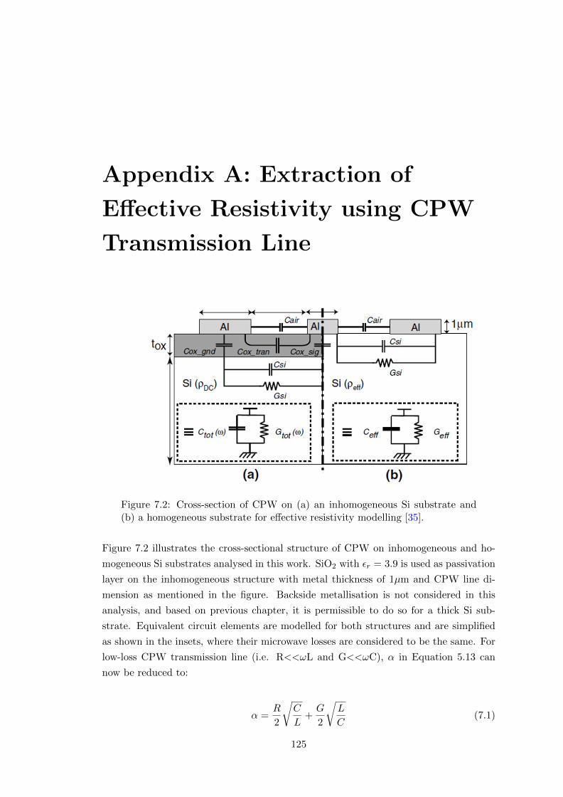
Appendix A: Extraction of
Effective Resistivity using CPW
Transmission Line
Figure 7.2: Cross-section of CPW on (a) an inhomogeneous Si substrate and(b) a homogeneous substrate for effective resistivity modelling [35].
Figure 7.2 illustrates the cross-sectional structure of CPW on inhomogeneous and ho-
mogeneous Si substrates analysed in this work. SiO2 with εr = 3.9 is used as passivation
layer on the inhomogeneous structure with metal thickness of 1µm and CPW line di-
mension as mentioned in the figure. Backside metallisation is not considered in this
analysis, and based on previous chapter, it is permissible to do so for a thick Si sub-
strate. Equivalent circuit elements are modelled for both structures and are simplified
as shown in the insets, where their microwave losses are considered to be the same. For
low-loss CPW transmission line (i.e. R<<ωL and G<<ωC), α in Equation 5.13 can
now be reduced to:
α =R
2
√C
L+G
2
√L
C(7.1)
125
126Chapter 7 Appendix A: Extraction of Effective Resistivity using CPW Transmission
Line
Assuming R to be the same for both cases (same Al metal line hence same conductor
loss, αC), the expression can be further approximated below to give substrate loss of:
αinh ≈Gtot
2
√L
Ctot; αeff ≈
Geff2
√L
Ceff(7.2)
for inhomogeneous CPW structure and effective structure, where only substrate losses
are considered and L is identical (due to same geometrical CPW dimension used). Since
substrate losses are also assumed to be the same, the relationship between inhomoge-
neous and effective structure is found to be:
Geff = Gtot
√CeffCtot
(7.3)
Effective capacitance, Ceff can be expressed in terms of air-filled capacitance, Co using
[110]:
εr,eff =CeffCo
(7.4)
where εeff is the effective relative permittivity and can be written down in terms of εr,Si
and filling factor, q:
εr,eff = 1 + q(εr,Si − 1) (7.5)
Meanwhile, the expression for effective conductance, Geff is as follows:
Geff = qCo
εoρeff(7.6)
where ρeff represents the effective resistivity of the structure.
Based on the expressions shown in Equation 7.3 to Equation 7.6, the equivalent effective
resistivity for an inhomogeneous structure is derived as:
ρeff =1
√εr,eff
(εr,eff − 1
εr,Si − 1
) √Coεo
√CtotGtot
(7.7)
where Ctot and Gtot are extracted from S-parameter data measured or simulated from
inhomogeneous structure.
Chapter 7 Appendix A: Extraction of Effective Resistivity using CPW TransmissionLine 127
Equation 7.7 shows that effective resistivity is strongly dependent on εr,eff and Co of the
structure. However, since the same geometrical line dimension is used on all analysed
substrates and the variation of oxide thickness considered in this work are within the
range where εr,eff remains unchanged, then these two parameters will be kept constant
throughout the whole analysis in this chapter alongside εo and εr,Si. Therefore, the
only dependency of ρeff will be coming from measured (or simulated) capacitance and
conductance of the inhomogeneous structure. Revisiting previous section where C and
G are derived from γ and Zc, and that αc,inh and αc,eff are the same, ρeff can then be
said to be purely dependent on the losses contributed by PSC effect.
To demonstrate the relationship between ρeff and CPW losses, Equation 7.7 is simplified
with a number of considerations made. First of all, by only considering an infinitely thick
Si substrate and ignoring backside metallisation, the structure can be treated as a direct
Al-Si CPW with effective relative permittivity [110]:
εr,eff ≈εr,Si
2(7.8)
and the corresponding Co for the case of SCPW >> WCPW is:
Co = 4 εoK(ko)
K(k′o)
≈ 4 εo (7.9)
Since γ = α + jβ and Zc is assumed to be 50Ω, expressions for Gtot and Ctot shown in
Equation 5.17 and Equation 5.18 respectively can be further broken down into:
G = Re
(γ
Zc
)=
α
50(7.10)
C = Im
(γZc
)2πf
=β
100πf(7.11)
Substituting Equation 7.10 and Equation 7.11 into Equation 7.7 gives:
ρeff =
√2
√εoεr,Si
εr,Si − 2
εr,Si − 1
√50√
2πf
√β
α(7.12)
where ρeff is seen to be linearly dependent on√β and inversely proportional to α and
√f .
SONNET simulation was performed on an oxide-free Al-Si CPW structure to verify the
connection between ρeff and CPW losses (α and β). Geometrical CPW dimension as
explained in Figure 3.5 in Chapter 5 was used in this simulation work, with SiO2 layer
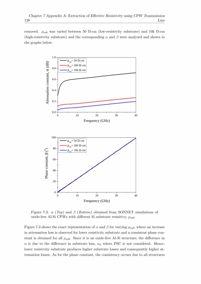
128Chapter 7 Appendix A: Extraction of Effective Resistivity using CPW Transmission
Line
removed. ρsub was varied between 50 Ω-cm (low-resistivity substrate) and 10k Ω-cm
(high-resistivity substrate) and the corresponding α and β were analysed and shown in
the graphs below.
0 1 0 2 0 3 0 4 00 . 0
0 . 2
0 . 4
0 . 6
0 . 8
1 . 0 ρ s u b = 5 0 Ω - c m ρ s u b = 3 6 0 Ω - c m ρ s u b = 1 0 k Ω - c m
Attenu
ation c
onstan
t, α (d
B)
F r e q u e n c y ( G H z )
0 1 0 2 0 3 0 4 00
2 0
4 0
6 0
8 0
1 0 0
Phase
const
ant, β
(0 )
F r e q u e n c y ( G H z )
ρ s u b = 5 0 Ω - c m ρ s u b = 3 6 0 Ω - c m ρ s u b = 1 0 k Ω - c m
Figure 7.3: α (Top) and β (Bottom) obtained from SONNET simulations ofoxide-free Al-Si CPWs with different Si substrate resisitivy, ρsub.
Figure 7.3 shows the exact representation of α and β for varying ρsub, where an increase
in attenuation loss is observed for lower resistivity substrate and a consistent phase con-
stant is obtained for all ρsub. Since it is an oxide-free Al-Si structure, the difference in
α is due to the difference in substrate loss, αd where PSC is not considered. Hence,
lower resistivity substrate produces higher substrate losses and consequently higher at-
tenuation losses. As for the phase constant, the consistency occurs due to all structures
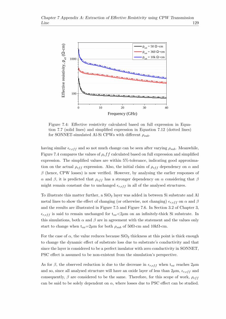
Chapter 7 Appendix A: Extraction of Effective Resistivity using CPW TransmissionLine 129
0 1 0 2 0 3 0 4 0
1 0 0
1 0 0 0Eff
ective
resis
tivity
, ρeff
(Ω-cm
)
F r e q u e n c y ( G H z )
ρ s u b = 5 0 Ω− c m ρ s u b = 3 6 0 Ω− c m ρ s u b = 1 0 k Ω− c m
Figure 7.4: Effective resistivity calculated based on full expression in Equa-tion 7.7 (solid lines) and simplified expression in Equation 7.12 (dotted lines)for SONNET-simulated Al-Si CPWs with different ρsub.
having similar εr,eff and so not much change can be seen after varying ρsub. Meanwhile,
Figure 7.4 compares the values of ρeff calculated based on full expression and simplified
expression. The simplified values are within 5%-tolerance, indicating good approxima-
tion on the actual ρeff expression. Also, the initial claim of ρeff dependency on α and
β (hence, CPW losses) is now verified. However, by analysing the earlier responses of
α and β, it is predicted that ρeff has a stronger dependency on α considering that β
might remain constant due to unchanged εr,eff in all of the analysed structures.
To illustrate this matter further, a SiO2 layer was added in between Si substrate and Al
metal lines to show the effect of changing (or otherwise, not changing) εr,eff on α and β
and the results are illustrated in Figure 7.5 and Figure 7.6. In Section 3.2 of Chapter 3,
εr,eff is said to remain unchanged for tox<2µm on an infinitely-thick Si substrate. In
this simulations, both α and β are in agreement with the statement and the values only
start to change when tox=2µm for both ρsub of 50Ω-cm and 10kΩ-cm.
For the case of α, the value reduces because SiO2 thickness at this point is thick enough
to change the dynamic effect of substrate loss due to substrate’s conductivity and that
since the layer is considered to be a perfect insulator with zero conductivity in SONNET,
PSC effect is assumed to be non-existent from the simulation’s perspective.
As for β, the observed reduction is due to the decrease in εr,eff when tox reaches 2µm
and so, since all analysed structure will have an oxide layer of less than 2µm, εr,eff and
consequently, β are considered to be the same. Therefore, for this scope of work, ρeff
can be said to be solely dependent on α, where losses due to PSC effect can be studied.
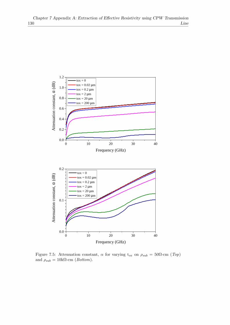
130Chapter 7 Appendix A: Extraction of Effective Resistivity using CPW Transmission
Line
0 1 0 2 0 3 0 4 00 . 0
0 . 2
0 . 4
0 . 6
0 . 8
1 . 0
1 . 2
Attenu
ation c
onstan
t, α (d
B)
F r e q u e n c y ( G H z )
t o x = 0 t o x = 0 . 0 2 µm t o x = 0 . 2 µm t o x = 2 µm t o x = 2 0 µm t o x = 2 0 0 µm
0 1 0 2 0 3 0 4 00 . 0
0 . 1
0 . 2
Attenu
ation c
onstan
t, α (d
B)
F r e q u e n c y ( G H z )
t o x = 0 t o x = 0 . 0 2 µm t o x = 0 . 2 µm t o x = 2 µm t o x = 2 0 µm t o x = 2 0 0 µm
Figure 7.5: Attenuation constant, α for varying tox on ρsub = 50Ω-cm (Top)and ρsub = 10kΩ-cm (Bottom).
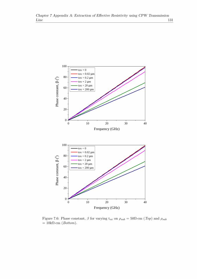
Chapter 7 Appendix A: Extraction of Effective Resistivity using CPW TransmissionLine 131
0 1 0 2 0 3 0 4 00
2 0
4 0
6 0
8 0
1 0 0
Phase
const
ant, β
(0 )
F r e q u e n c y ( G H z )
t o x = 0 t o x = 0 . 0 2 µm t o x = 0 . 2 µm t o x = 2 µm t o x = 2 0 µm t o x = 2 0 0 µm
0 1 0 2 0 3 0 4 00
2 0
4 0
6 0
8 0
1 0 0
Phase
const
ant, β
(0 )
F r e q u e n c y ( G H z )
t o x = 0 t o x = 0 . 0 2 µm t o x = 0 . 2 µm t o x = 2 µm t o x = 2 0 µm t o x = 2 0 0 µm
Figure 7.6: Phase constant, β for varying tox on ρsub = 50Ω-cm (Top) and ρsub= 10kΩ-cm (Bottom).
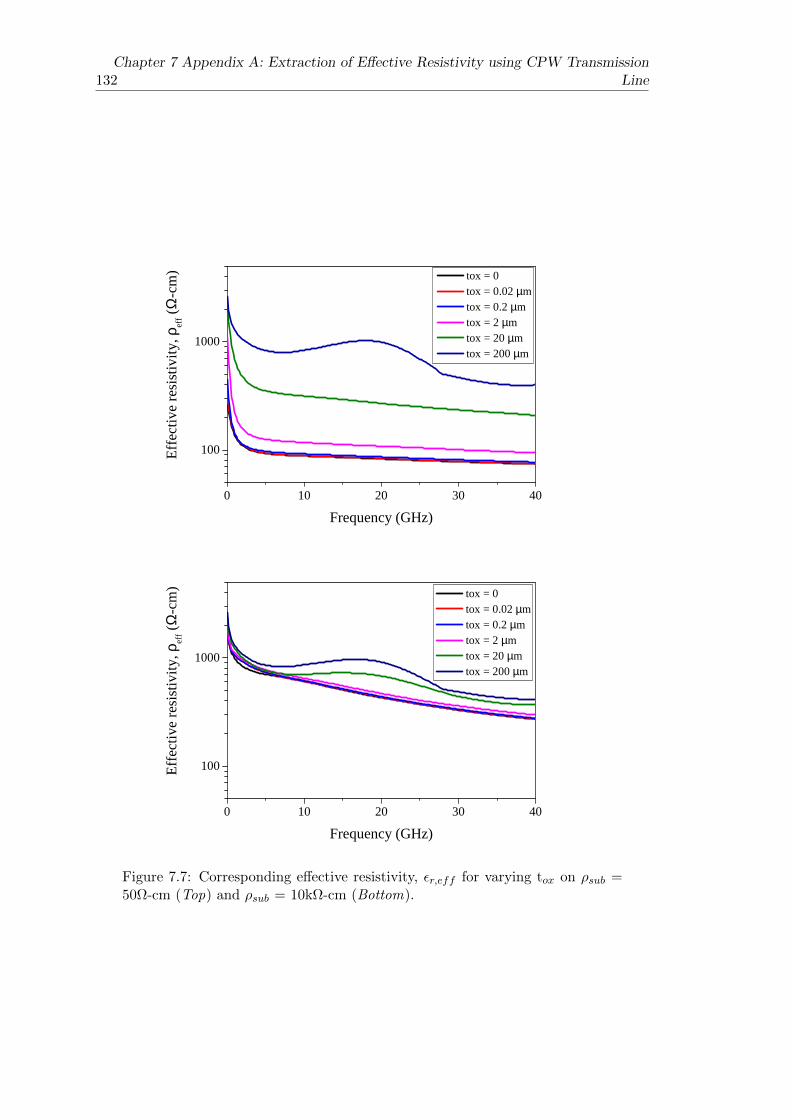
132Chapter 7 Appendix A: Extraction of Effective Resistivity using CPW Transmission
Line
0 1 0 2 0 3 0 4 0
1 0 0
1 0 0 0
Effect
ive re
sistiv
ity, ρ
eff (Ω
-cm)
F r e q u e n c y ( G H z )
t o x = 0 t o x = 0 . 0 2 µm t o x = 0 . 2 µm t o x = 2 µm t o x = 2 0 µm t o x = 2 0 0 µm
0 1 0 2 0 3 0 4 0
1 0 0
1 0 0 0
Effect
ive re
sistiv
ity, ρ
eff (Ω
-cm)
F r e q u e n c y ( G H z )
t o x = 0 t o x = 0 . 0 2 µm t o x = 0 . 2 µm t o x = 2 µm t o x = 2 0 µm t o x = 2 0 0 µm
Figure 7.7: Corresponding effective resistivity, εr,eff for varying tox on ρsub =50Ω-cm (Top) and ρsub = 10kΩ-cm (Bottom).
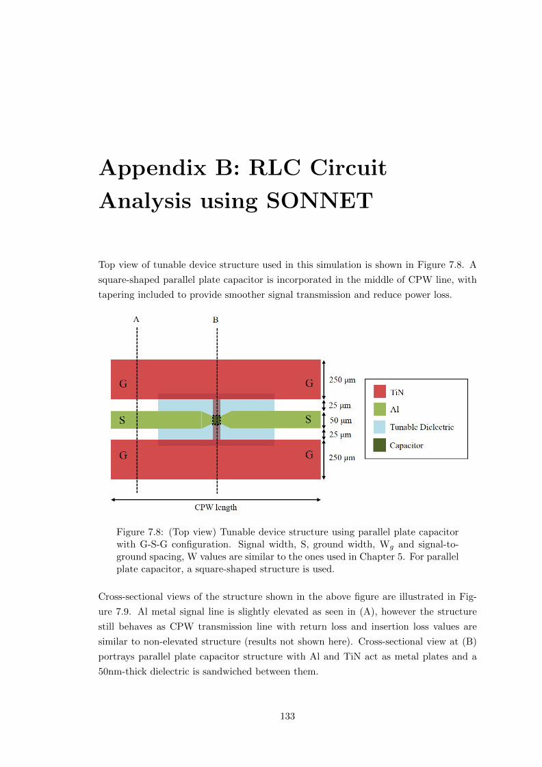
Appendix B: RLC Circuit
Analysis using SONNET
Top view of tunable device structure used in this simulation is shown in Figure 7.8. A
square-shaped parallel plate capacitor is incorporated in the middle of CPW line, with
tapering included to provide smoother signal transmission and reduce power loss.
Figure 7.8: (Top view) Tunable device structure using parallel plate capacitorwith G-S-G configuration. Signal width, S, ground width, Wg and signal-to-ground spacing, W values are similar to the ones used in Chapter 5. For parallelplate capacitor, a square-shaped structure is used.
Cross-sectional views of the structure shown in the above figure are illustrated in Fig-
ure 7.9. Al metal signal line is slightly elevated as seen in (A), however the structure
still behaves as CPW transmission line with return loss and insertion loss values are
similar to non-elevated structure (results not shown here). Cross-sectional view at (B)
portrays parallel plate capacitor structure with Al and TiN act as metal plates and a
50nm-thick dielectric is sandwiched between them.
133
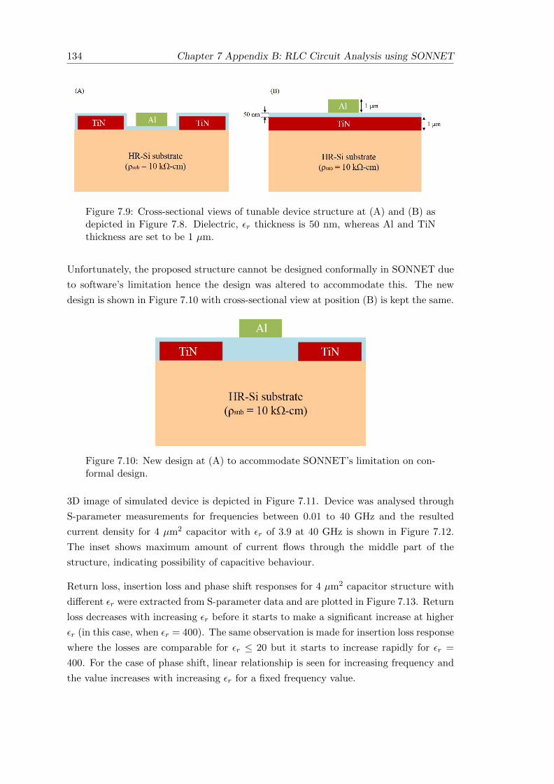
134 Chapter 7 Appendix B: RLC Circuit Analysis using SONNET
Figure 7.9: Cross-sectional views of tunable device structure at (A) and (B) asdepicted in Figure 7.8. Dielectric, εr thickness is 50 nm, whereas Al and TiNthickness are set to be 1 µm.
Unfortunately, the proposed structure cannot be designed conformally in SONNET due
to software’s limitation hence the design was altered to accommodate this. The new
design is shown in Figure 7.10 with cross-sectional view at position (B) is kept the same.
Figure 7.10: New design at (A) to accommodate SONNET’s limitation on con-formal design.
3D image of simulated device is depicted in Figure 7.11. Device was analysed through
S-parameter measurements for frequencies between 0.01 to 40 GHz and the resulted
current density for 4 µm2 capacitor with εr of 3.9 at 40 GHz is shown in Figure 7.12.
The inset shows maximum amount of current flows through the middle part of the
structure, indicating possibility of capacitive behaviour.
Return loss, insertion loss and phase shift responses for 4 µm2 capacitor structure with
different εr were extracted from S-parameter data and are plotted in Figure 7.13. Return
loss decreases with increasing εr before it starts to make a significant increase at higher
εr (in this case, when εr = 400). The same observation is made for insertion loss response
where the losses are comparable for εr ≤ 20 but it starts to increase rapidly for εr =
400. For the case of phase shift, linear relationship is seen for increasing frequency and
the value increases with increasing εr for a fixed frequency value.
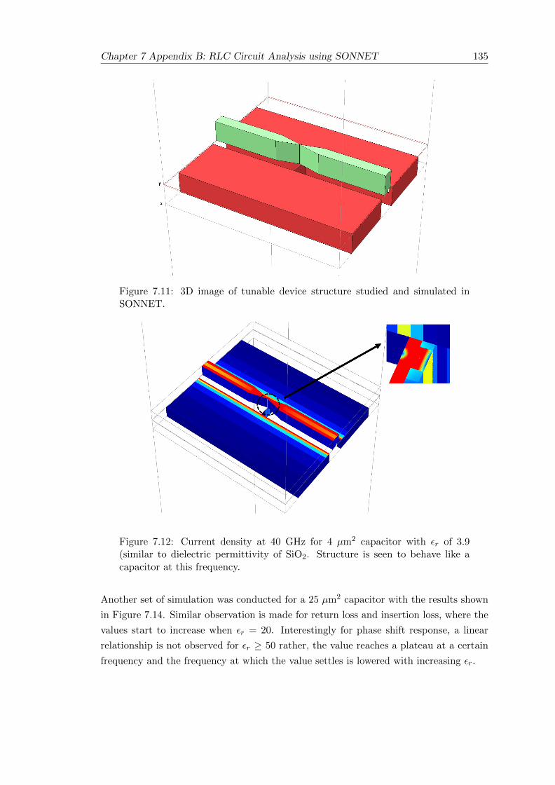
Chapter 7 Appendix B: RLC Circuit Analysis using SONNET 135
Figure 7.11: 3D image of tunable device structure studied and simulated inSONNET.
Figure 7.12: Current density at 40 GHz for 4 µm2 capacitor with εr of 3.9(similar to dielectric permittivity of SiO2. Structure is seen to behave like acapacitor at this frequency.
Another set of simulation was conducted for a 25 µm2 capacitor with the results shown
in Figure 7.14. Similar observation is made for return loss and insertion loss, where the
values start to increase when εr = 20. Interestingly for phase shift response, a linear
relationship is not observed for εr ≥ 50 rather, the value reaches a plateau at a certain
frequency and the frequency at which the value settles is lowered with increasing εr.
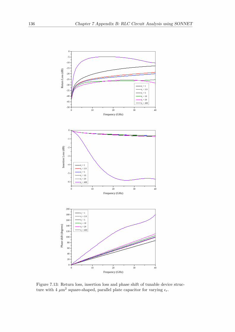
136 Chapter 7 Appendix B: RLC Circuit Analysis using SONNET
0 1 0 2 0 3 0 4 0- 5 0- 4 5- 4 0- 3 5- 3 0- 2 5- 2 0- 1 5- 1 0- 50
Retur
n Loss
(dB)
F r e q u e n c y ( G H z )
εr = 1 εr = 3 . 9 εr = 5 εr = 1 0 εr = 2 0 εr = 4 0 0
0 1 0 2 0 3 0 4 0
- 6
- 5
- 4
- 3
- 2
- 1
0
εr = 1 εr = 3 . 9 εr = 5 εr = 1 0 εr = 2 0 εr = 4 0 0
Insert
ion Lo
ss (dB
)
F r e q u e n c y ( G H z )
0 1 0 2 0 3 0 4 00
2 04 06 08 0
1 0 01 2 01 4 01 6 01 8 02 0 0
εr = 1 εr = 3 . 9 εr = 5 εr = 1 0 εr = 2 0 εr = 4 0 0
Phase
shift
(degre
es)
F r e q u e n c y ( G H z )
Figure 7.13: Return loss, insertion loss and phase shift of tunable device struc-ture with 4 µm2 square-shaped, parallel plate capacitor for varying εr.
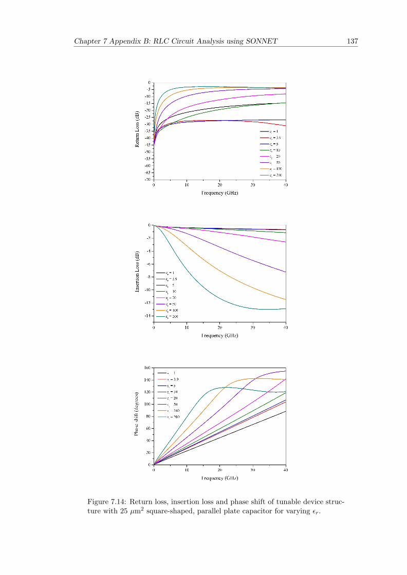
Chapter 7 Appendix B: RLC Circuit Analysis using SONNET 137
Figure 7.14: Return loss, insertion loss and phase shift of tunable device struc-ture with 25 µm2 square-shaped, parallel plate capacitor for varying εr.

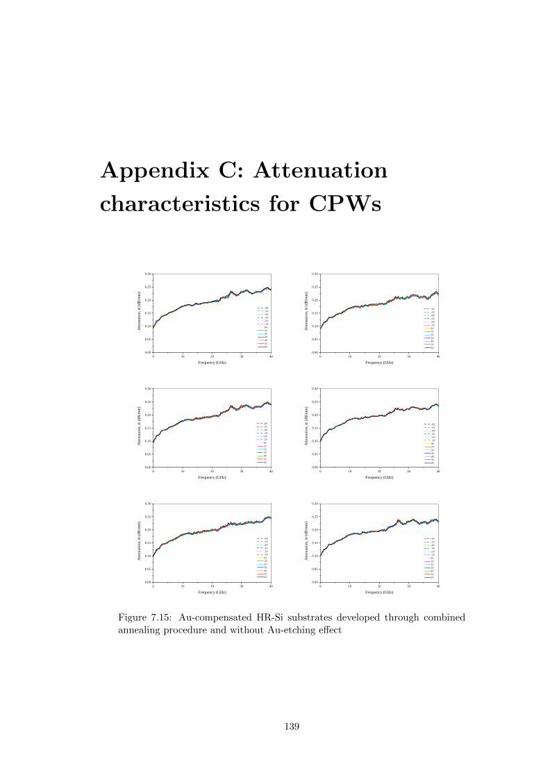
Appendix C: Attenuation
characteristics for CPWs
0 1 0 2 0 3 0 4 00 . 0 0
0 . 0 5
0 . 1 0
0 . 1 5
0 . 2 0
0 . 2 5
0 . 3 0
- 6 V - 5 V - 4 V - 3 V - 2 V - 1 V 0 V 1 V 2 V 3 V 4 V 5 V 6 V
Attenu
ation, α
(dB/m
m)
F r e q u e n c y ( G H z )0 1 0 2 0 3 0 4 0
0 . 0 0
0 . 0 5
0 . 1 0
0 . 1 5
0 . 2 0
0 . 2 5
0 . 3 0
- 6 V - 5 V - 4 V - 3 V - 2 V - 1 V 0 V 1 V 2 V 3 V 4 V 5 V 6 V
Attenu
ation, α
(dB/m
m)
F r e q u e n c y ( G H z )
Figure 7.15: Au-compensated HR-Si substrates developed through combinedannealing procedure and without Au-etching effect
139
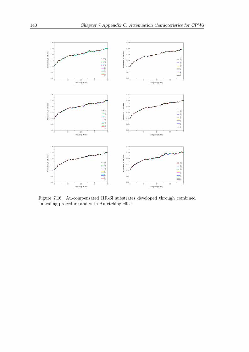
140 Chapter 7 Appendix C: Attenuation characteristics for CPWs
0 1 0 2 0 3 0 4 00 . 0 0
0 . 0 5
0 . 1 0
0 . 1 5
0 . 2 0
0 . 2 5
0 . 3 0
- 6 V - 5 V - 4 V - 3 V - 2 V - 1 V 0 V 1 V 2 V 3 V 4 V 5 V 6 V
Attenu
ation, α
(dB/m
m)
F r e q u e n c y ( G H z )0 1 0 2 0 3 0 4 0
0 . 0 0
0 . 0 5
0 . 1 0
0 . 1 5
0 . 2 0
0 . 2 5
0 . 3 0
- 6 V - 5 V - 4 V - 3 V - 2 V - 1 V 0 V 1 V 2 V 3 V 4 V 5 V 6 V
Attenu
ation, α
(dB/m
m)
F r e q u e n c y ( G H z )
Figure 7.16: Au-compensated HR-Si substrates developed through combinedannealing procedure and with Au-etching effect
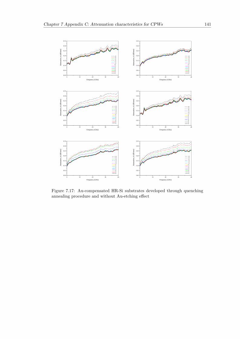
Chapter 7 Appendix C: Attenuation characteristics for CPWs 141
0 1 0 2 0 3 0 4 00 . 0 0
0 . 0 5
0 . 1 0
0 . 1 5
0 . 2 0
0 . 2 5
0 . 3 0
0 . 3 5
- 6 V - 5 V - 4 V - 3 V - 2 V - 1 V 0 V 1 V 2 V 3 V 4 V 5 V 6 V
Attenu
ation, α
(dB/m
m)
F r e q u e n c y ( G H z )0 1 0 2 0 3 0 4 0
0 . 0 0
0 . 0 5
0 . 1 0
0 . 1 5
0 . 2 0
0 . 2 5
0 . 3 0
0 . 3 5
- 6 V - 5 V - 4 V - 3 V - 2 V - 1 V 0 V 1 V 2 V 3 V 4 V 5 V 6 V
Attenu
ation, α
(dB/m
m)
F r e q u e n c y ( G H z )
0 1 0 2 0 3 0 4 00 . 0 0
0 . 0 5
0 . 1 0
0 . 1 5
0 . 2 0
0 . 2 5
0 . 3 0
0 . 3 5
- 6 V - 5 V - 4 V - 3 V - 2 V - 1 V 0 V 1 V 2 V 3 V 4 V 5 V 6 V
Attenu
ation, α
(dB/m
m)
F r e q u e n c y ( G H z )0 1 0 2 0 3 0 4 0
0 . 0 0
0 . 0 5
0 . 1 0
0 . 1 5
0 . 2 0
0 . 2 5
0 . 3 0
0 . 3 5
- 6 V - 5 V - 4 V - 3 V - 2 V - 1 V 0 V 1 V 2 V 3 V 4 V 5 V 6 V
Attenu
ation, α
(dB/m
m)F r e q u e n c y ( G H z )
0 1 0 2 0 3 0 4 00 . 0 0
0 . 0 5
0 . 1 0
0 . 1 5
0 . 2 0
0 . 2 5
0 . 3 0
0 . 3 5
- 6 V - 5 V - 4 V - 3 V - 2 V - 1 V 0 V 1 V 2 V 3 V 4 V 5 V 6 V
Attenu
ation, α
(dB/m
m)
F r e q u e n c y ( G H z )0 1 0 2 0 3 0 4 0
0 . 0 0
0 . 0 5
0 . 1 0
0 . 1 5
0 . 2 0
0 . 2 5
0 . 3 0
0 . 3 5
- 6 V - 5 V - 4 V - 3 V - 2 V - 1 V 0 V 1 V 2 V 3 V 4 V 5 V 6 V
Attenu
ation, α
(dB/m
m)
F r e q u e n c y ( G H z )
Figure 7.17: Au-compensated HR-Si substrates developed through quenchingannealing procedure and without Au-etching effect
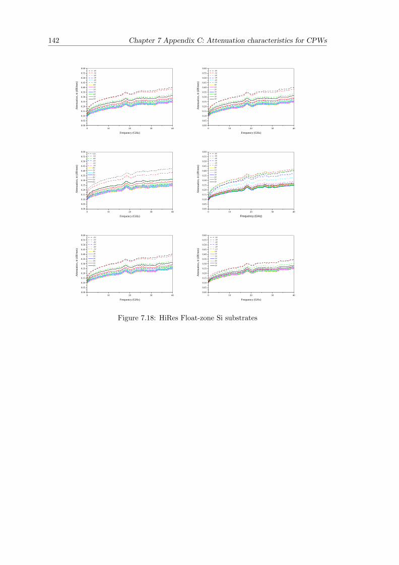
142 Chapter 7 Appendix C: Attenuation characteristics for CPWs
0 1 0 2 0 3 0 4 00 . 0 00 . 0 50 . 1 00 . 1 50 . 2 00 . 2 50 . 3 00 . 3 50 . 4 00 . 4 50 . 5 00 . 5 50 . 6 0
- 6 V - 5 V - 4 V - 3 V - 2 V - 1 V 0 V 1 V 2 V 3 V 4 V 5 V 6 V
Attenu
ation, α
(dB/m
m)
F r e q u e n c y ( G H z )0 1 0 2 0 3 0 4 0
0 . 0 00 . 0 50 . 1 00 . 1 50 . 2 00 . 2 50 . 3 00 . 3 50 . 4 00 . 4 50 . 5 00 . 5 50 . 6 0
- 6 V - 5 V - 4 V - 3 V - 2 V - 1 V 0 V 1 V 2 V 3 V 4 V 5 V 6 V
Attenu
ation, α
(dB/m
m)
F r e q u e n c y ( G H z )
0 1 0 2 0 3 0 4 00 . 0 00 . 0 50 . 1 00 . 1 50 . 2 00 . 2 50 . 3 00 . 3 50 . 4 00 . 4 50 . 5 00 . 5 50 . 6 0 - 6 V
- 5 V - 4 V - 3 V - 2 V - 1 V 0 V 1 V 2 V 3 V 4 V 5 V 6 V
Attenu
ation, α
(dB/m
m)
F r e q u e n c y ( G H z )0 1 0 2 0 3 0 4 0
0 . 0 00 . 0 50 . 1 00 . 1 50 . 2 00 . 2 50 . 3 00 . 3 50 . 4 00 . 4 50 . 5 00 . 5 50 . 6 0 - 6 V
- 5 V - 4 V - 3 V - 2 V - 1 V 0 V 1 V 2 V 3 V 4 V 5 V 6 V
Attenu
ation, α
(dB/m
m)
F r e q u e n c y ( G H z )
0 1 0 2 0 3 0 4 00 . 0 00 . 0 50 . 1 00 . 1 50 . 2 00 . 2 50 . 3 00 . 3 50 . 4 00 . 4 50 . 5 00 . 5 50 . 6 0
- 6 V - 5 V - 4 V - 3 V - 2 V - 1 V 0 V 1 V 2 V 3 V 4 V 5 V 6 V
Attenu
ation, α
(dB/m
m)
F r e q u e n c y ( G H z )0 1 0 2 0 3 0 4 0
0 . 0 00 . 0 50 . 1 00 . 1 50 . 2 00 . 2 50 . 3 00 . 3 50 . 4 00 . 4 50 . 5 00 . 5 50 . 6 0
- 6 V - 5 V - 4 V - 3 V - 2 V - 1 V 0 V 1 V 2 V 3 V 4 V 5 V 6 V
Attenu
ation, α
(dB/m
m)
F r e q u e n c y ( G H z )
Figure 7.18: HiRes Float-zone Si substrates
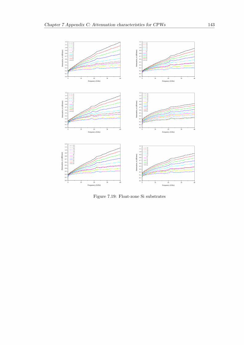
Chapter 7 Appendix C: Attenuation characteristics for CPWs 143
0 1 0 2 0 3 0 4 00 . 00 . 10 . 20 . 30 . 40 . 50 . 60 . 70 . 80 . 91 . 01 . 11 . 2
Attenu
ation, α
(dB/m
m)
F r e q u e n c y ( G H z )
- 6 V - 5 V - 4 V - 3 V - 2 V - 1 V 0 V 1 V 2 V 3 V 4 V 5 V 6 V
0 1 0 2 0 3 0 4 00 . 00 . 10 . 20 . 30 . 40 . 50 . 60 . 70 . 80 . 91 . 01 . 11 . 2
- 6 V - 5 V - 4 V - 3 V - 2 V - 1 V 0 V 1 V 2 V 3 V 4 V 5 V 6 V
Attenu
ation, α
(dB/m
m)
F r e q u e n c y ( G H z )
0 1 0 2 0 3 0 4 00 . 00 . 10 . 20 . 30 . 40 . 50 . 60 . 70 . 80 . 91 . 01 . 11 . 2
- 6 V - 5 V - 4 V - 3 V - 2 V - 1 V 0 V 1 V 2 V 3 V 4 V 5 V 6 V
Attenu
ation, α
(dB/m
m)
F r e q u e n c y ( G H z )0 1 0 2 0 3 0 4 0
0 . 00 . 10 . 20 . 30 . 40 . 50 . 60 . 70 . 80 . 91 . 01 . 11 . 2
- 6 V - 5 V - 4 V - 3 V - 2 V - 1 V 0 V 1 V 2 V 3 V 4 V 5 V 6 V
Attenu
ation, α
(dB/m
m)F r e q u e n c y ( G H z )
0 1 0 2 0 3 0 4 00 . 00 . 10 . 20 . 30 . 40 . 50 . 60 . 70 . 80 . 91 . 01 . 11 . 2
- 6 V - 5 V - 4 V - 3 V - 2 V - 1 V 0 V 1 V 2 V 3 V 4 V 5 V 6 V
Attenu
ation, α
(dB/m
m)
F r e q u e n c y ( G H z )0 1 0 2 0 3 0 4 0
0 . 00 . 10 . 20 . 30 . 40 . 50 . 60 . 70 . 80 . 91 . 01 . 11 . 2
- 6 V - 5 V - 4 V - 3 V - 2 V - 1 V 0 V 1 V 2 V 3 V 4 V 5 V 6 V
Attenu
ation, α
(dB/m
m)
F r e q u e n c y ( G H z )
Figure 7.19: Float-zone Si substrates