Embed Size (px)
Citation preview
1170007
UNIVERSITY OF SURREY LIBRARY

ProQuest Number: All rights reserved
INFORMATION TO ALL USERS The quality of this reproduction is dependent upon the quality of the copy submitted.
In the unlikely event that the author did not send a com plete manuscript and there are missing pages, these will be noted. Also, if material had to be removed,
a note will indicate the deletion.
uestProQuest 10130240
Published by ProQuest LLO (2017). Copyright of the Dissertation is held by the Author.
All rights reserved.This work is protected against unauthorized copying under Title 17, United States C ode
Microform Edition © ProQuest LLO.
ProQuest LLO.789 East Eisenhower Parkway
P.Q. Box 1346 Ann Arbor, Ml 4 81 06 - 1346
The Temperature and Pressure Dependence of Electron
Transport in Plastically Relaxed InxGa^xAs- img-aNS
by
Mehmet Kasap
A thesis submitted to the Faculty of Science
at the University of Surrey for the Degree of
Doctor of Philosophy.
Department of Physics
University of Surrey
December 1993.
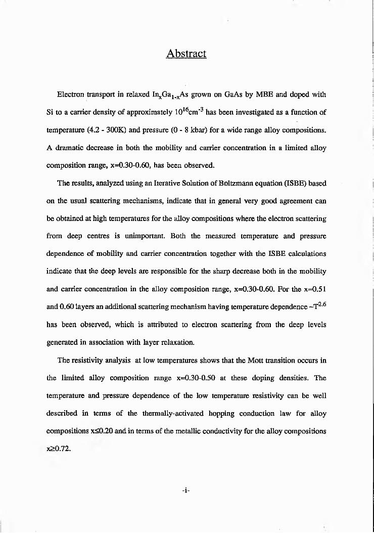
Abstract
Electron transport in relaxed Ii^Ga^As grown on GaAs by MBE and doped with
Si to a carrier density of approximately 1016cm'3 has been investigated as a function of
temperature (4.2 - 300K) and pressure ( 0- 8 kbar) for a wide range alloy compositions.
A dramatic decrease in both the mobility and carrier concentration in a limited alloy
composition range, x=0.30-0.60, has been observed.
The results, analyzed using an Iterative Solution of Boltzmann equation (ISBE) based
on the usual scattering mechanisms, indicate that in general very good agreement can
be obtained at high temperatures for the alloy compositions where the electron scattering
from deep centres is unimportant. Both the measured temperature and pressure
dependence of mobility and carrier concentration together with the ISBE calculations
indicate that the deep levels are responsible for the sharp decrease both in the mobility
and carrier concentration in the alloy composition range, x=0.30-0.60. For the x=0.51
and 0.60 layers an additional scattering mechanism having temperature dependence ~T2,6
has been observed, which is attributed to electron scattering from the deep levels
generated in association with layer relaxation.
The resistivity analysis at low temperatures shows that the Mott transition occurs in
the limited alloy composition range x=0.30-0.50 at these doping densities. The
temperature and pressure dependence of the low temperature resistivity can be well
described in terms of the thermally-activated hopping conduction law for alloy
compositions x<0.20 and in terms of the metallic conductivity for the alloy compositions
x>0.72.
-i-
A c k n o w l e d g e m e n t s
The work reported in this thesis was carried out in the Department of Physics at the
University of Surrey.
The author would like to express his sincere thanks to Dr. D Lancefield, under whose
supervision the work was performed, for his continuous help, excellent guidance and
good humour. Thanks are also due to the University of Gazi, Turkey, for their financial
support.
The author also wishes to thank Professor A R Adams who is the ODM research
group leader, B J Gunney, M R Crowe, J R Downes and the rest of the ODM group for
useful discussions and their help.
Finally the author would also like to thank his wife for her moral support during the
period of this research.
C o n te n ts
Abstract i
Acknowledgements ii
Contents in
C h a p t e r 1
I n t r o d u c t i o n 1
C h a p t e r 2
B a n d S t r u c t u r e a n d M a t e r i a l s P a r a m e t e r 3
2.1 Crystal Structure 3
2.2 Band Structure 3
2.2.1 The k.£ Theory 7
2.2.2 The Direct Band Gap E0 and Effective Mass m* 8
2.2.3 The Temperature Dependence of Direct Band Gap E0 and
Effective Mass m 9
2.4 Pressure Dependence of Band Gap and Effective Mass 11
2.5 The Effects of Impurities on the Band Structure 14
2.6 Material Properties and More Material Parameters 16
-iii-
L o w F i e l d T r a n s p o r t T h e o r y 2 4
3.1 Introduction 24
3.2 Electron Scattering 24
3.3 The Boltzmann Equation 25
3.3.1 Introduction to the Boltzmann Equation 25
3.3.2 Relaxation Time Approximation 27
3.3.3 Iterative Solution of the Boltzmann Equation 30
3.4 Scattering Mechanisms 32
3.4.1 Deformation Potential Scattering 32
3.4.2 Piezoelectric Potential Scattering 32
3.4.3 Polar Optical Phonon Scattering 33
3.4.4 Ionized Impurity Scattering 34
3.4.4.1 Introduction 34
3.4.4.2 Scattering by Random Impurity Distributions 34
3.4.5 Neutral Impurity Scattering 36
3.4.6 Alloy Scattering 37
3.5 Impurity Conduction and the Hopping Process 37
C h a p t e r 4
A p p a r a t u s a n d E x p e r i m e n t a l T e c h n i q u e s 4 1
4.1 Introduction 41
4.2 Sample Preparation 41
C h a p t e r 3
4.2.1 Clover Leaf Preparation by Etching 41
-iv-
4.3 Resistivity and Hall Coefficient Measurements 43
4.4 Cryostat and Temperature Control System 46
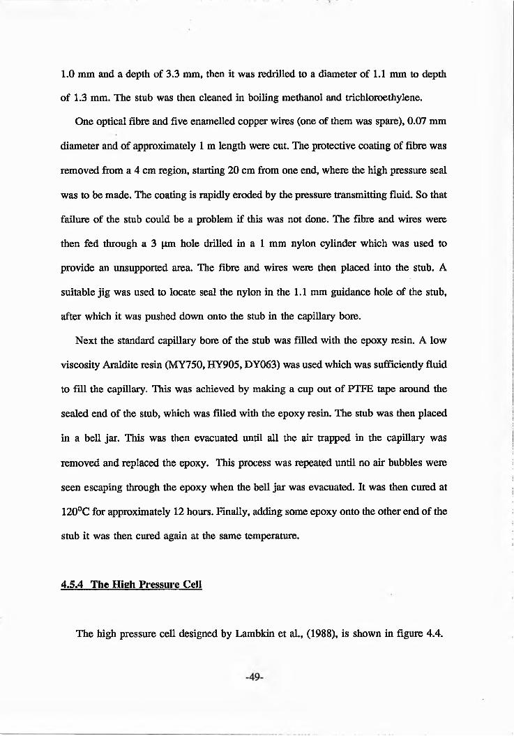
4.5 High Pressure Apparatus 47
4.5.1 Introduction 47
4.5.2 Piston and Cylinder Apparatus 47
4.5.3 The Use of the Three-way Harwood Coupler and the Stub 48
4.5.4 The High Pressure Cell 49
C h a p t e r 5
T e m p e r a t u r e D e p e n d e n c e o f H a l l M o b i l i t y a n d C a r r i e r
C o n c e n t r a t i o n i n I n x G a 1-xA s 5 5
5.1 Introduction 55
5.2 The Composition Dependence of Hall mobility and Carrier
Concentration 56
5.3 Temperature Dependence of Mobility and Carrier Concentration 62
5.4 Temperature Dependence of Mobility and Carrier Concentration
in the x=0.51 and 0.60 Samples 71
5.5 Conclusions 75
C h a p t e r 6
T e m p e r a t u r e a n d P r e s s u r e D e p e n d e n c e o f H a l l M o b i l i t y
a n d C a r r i e r C o n c e n t r a t i o n 7 7
4.2.2 Contacts Fabrication 42
-v-
6.1 Introduction 77
6.2 Room Temperature Pressure dependence of Carrier Concentration
and Mobility 77
6.3 Temperature and Pressure Dependence of Hall Mobility and
Carrier Concentration 86
6.4 Temperature and Pressure Dependence of Mobility and Carrier
Concentration in the x=0.51 and 0.60 Samples 97
6.5 Conclusions 102
C h a p t e r 7
I m p u r i t y C o n d u c t i o n i n I n x G a 1-xA s 1 0 4
7.1 Introduction 104
7.2 Impurity Conduction at x<0.20 108
7.3 Impurity Conduction at x>0.50 112
7.4 Conclusions 115
C h a p t e r 8
C o n c l u s io n s a n d R e c o m m e n d a t i o n s f o r F u r t h e r W o r k 1 1 7
R e f e r e n c e s 1 2 0
-v i-
C h a p t e r 1
Introduction
The alloys of semiconducting binary compounds are becoming increasingly important
for technological applications. Technologically desirable properties, which can not be
obtained from the binary compounds, may be derived from ternary alloys. InxGaj_xAs
is an important ternary semiconductor that finds widespread applications in various high
speed electronic and optoelectronic devices, [Nag, 1984 and Adachi, 1992]. In particular,
relaxed Ir^Ga^As grown on GaAs is of interest as a "substrate" with a variable lattice
constant. This would allow, for example, GaAs/InxGa1.xAs structures for both lasers and
high hole mobility transistors to be grown in both under compressive and tensile strain
as appropriate.
The demand of growing electronic industry requires the semiconductor materials to
be characterized. A common method of characterizing semiconductor materials is by
Hall effect and resistivity measurements. These measurements allow Hall mobility and
carrier concentration to be obtained. Both parameters can be used to characterise the
microscopic quality of semiconductors. Accurate comparisons between experimental
electron mobility and theoretical calculations are of great importance for determining the
impurity contents of material and the important electron scattering mechanisms.
In this thesis we investigate the electron mobility of thick InxGaj.xAs layers as a
function of temperature (4.2-300K) and pressure (0-8 kbar) for a wide range of alloy
compositions. Pressure is used to increase the direct band gap and consequently the
electron effective mass. This allows the important scattering mechanisms to be studied
as a function of effective mass and temperature, [Lancefield et al., 1987].
The organisation of this thesis is as follows. In chapter 2 material parameters and
their temperature and pressure dependencies are described. Chapter 3 reviews the low-
field transport theory including the individual scattering mechanisms and impurity band
conduction, while in chapter 4 the experimental apparatus and techniques used are
described. The temperature dependence of mobility and carrier concentration as well as
their composition dependencies are discussed in chapter 5. Chapter 6 discuses both
temperature and pressure dependence of mobility and carrier concentration for a wide
range of alloy compositions, while in chapter 7 the impurity band conduction at low
temperatures is discussed. Finally, in chapter 8 some conclusions are drawn and
guidelines for further work in this area are suggested.
Band Structure and Material Parameters
C h a p t e r 2
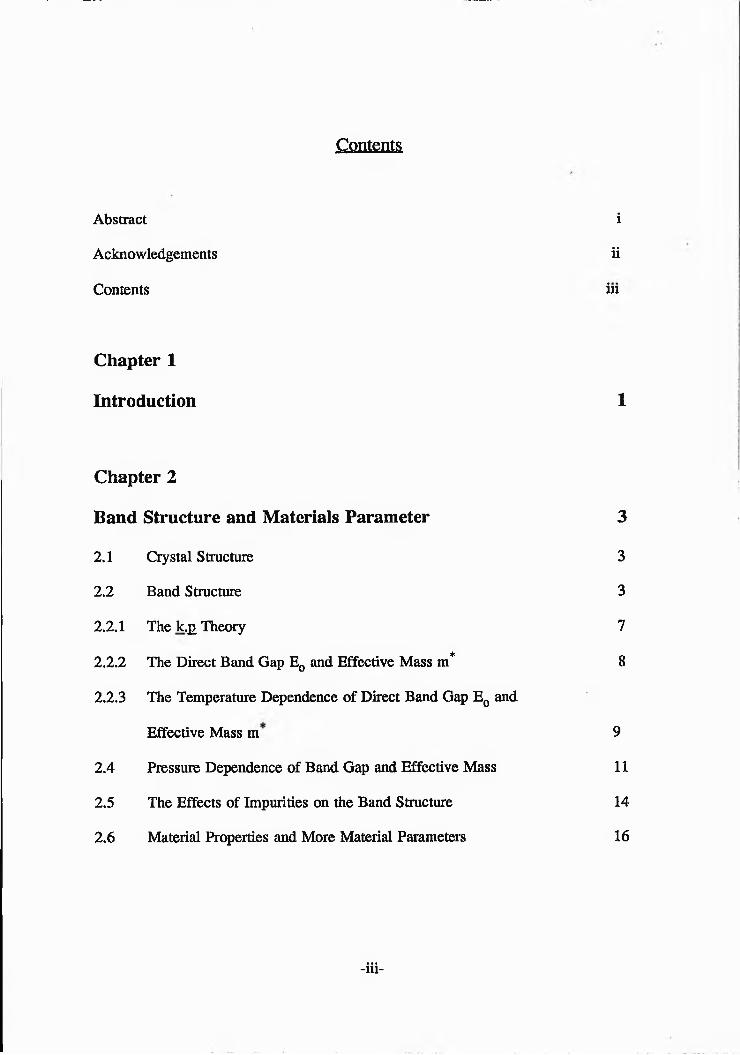
2.1 Crystal Structure
The election transport properties of semiconductors are strongly dependent on the
energy band structure and, therefore, crystal structure. Most of the III-V compounds,
and in particular fr^Ga^ As, form crystals with the zinc-blende arrangement. In this
structure each atom is surrounded by four equidistant nearest neighbours which lie at
the comers of the tetrahedron. The unit cell for this structure is given in figure 2.1.
In the case of ternary or quaternary alloy systems, the lattice constant (a) is known
to obey well Vegard’s law, i.e., to vary linearly with composition, [Nohary et al., 1978].
Therefore it can be calculated for the InxGaFxAs system as
a ( x ) = a i n a s x + a G o * B <1 " x > 2 . 1 . 1
2.2 Band Structure
The band structure of a material is usually obtained by solving the Schrodinger
equation and generally presented by plotting the energy of the electron E, for values of
-3-
the wave vector k, limited to within the first Brillouin zone. The energy bands of solids
have been studied theoretically using a variety of numerical methods. For
semiconductors the three methods most frequently used are the orthogonalized
plane-wave method (OPW), [Allen, 1955 and Herman, 1955], the pseudo-potential
method, [Phillips, 1958], and the k.p method, [Chelikowsky and Cohen, 1976].
Any semiconductor has forbidden and allowed energy regions because of the periodic
nature of the semiconductor’s crystal lattice. Energy regions are permitted above and
below this energy gap (band gap) which is the most important parameter to describe
many properties semiconductor materials.
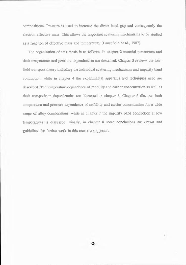
The band structure of a semiconductor is basically a function of crystal symmetry.
The most important symmetry points are F, X and L (high-symmetry points) in the
Brillouin zone. The most important features of the band structure are the positions of the
valence band and the conduction band extreme. The conduction band structure of most
compounds exhibits the lowest minima at the T point and the next two minima occur
at the X and L points while a valence band maximum always occurs at the F point,
[Aspens, 1976 and Vinson et al., 1976]. If the highest maxima and lowest minima occur
at the same point (at the F point) in the Brillouin zone, the crystal is called a direct gap
material and if this is not so it is called indirect gap material.
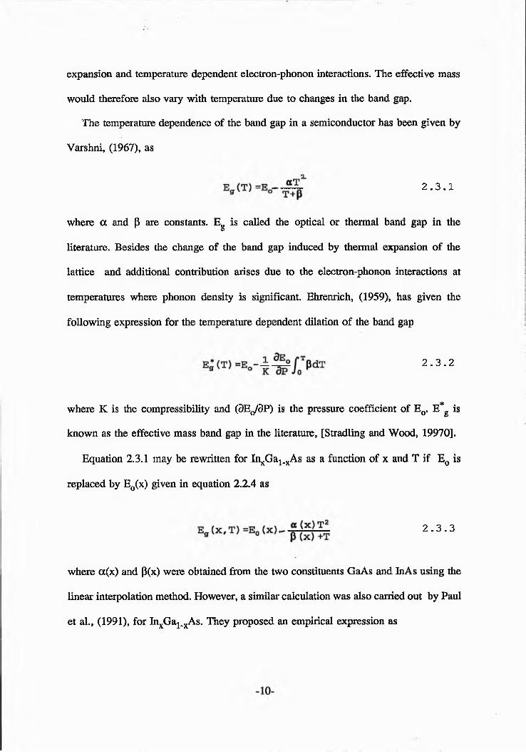
The materials investigated in this work are direct gap materials. Band structures of
some important semiconductors have been given by Chelikowsky and Cohen, (1976).
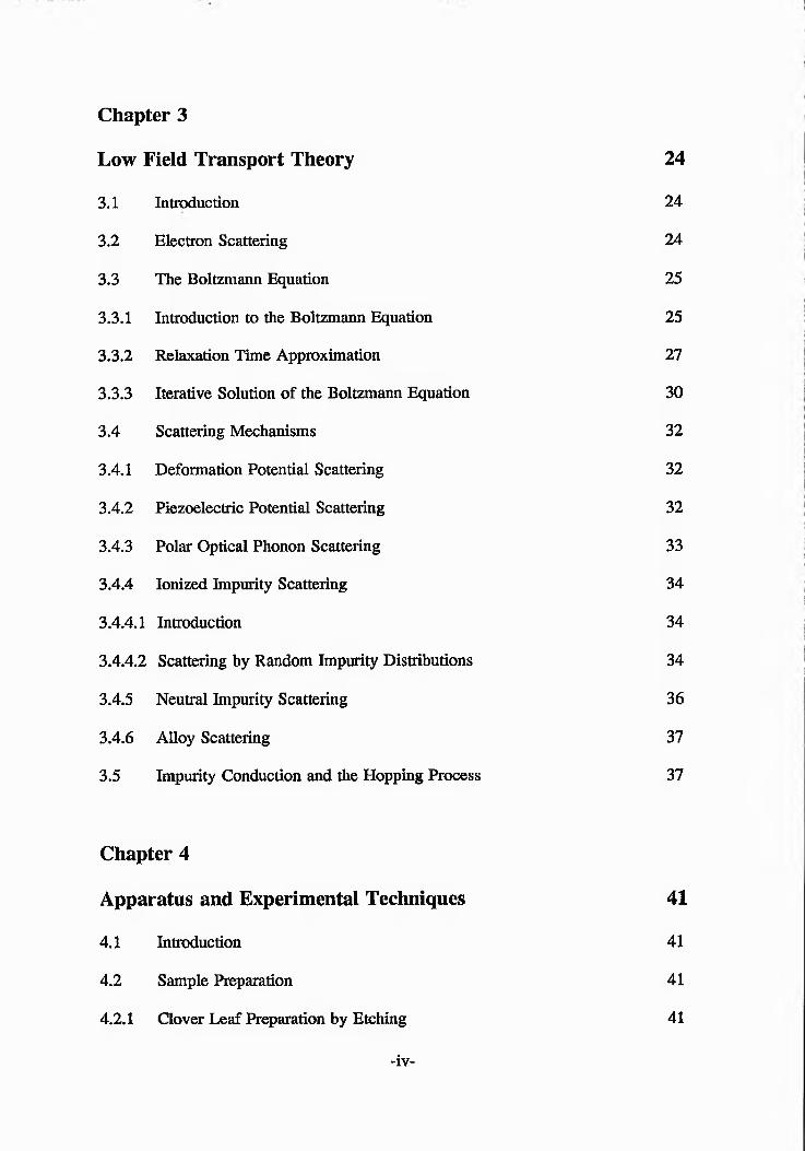
Figure 2.2 shows the schematic band structure of GaAs and InAs.
When we are dealing with low-field transport phenomena, it is generally sufficient
to be concerned with the lowest minima or the highest maxima. They play a key role
in determining the observable properties of semiconductor materials because these
Figure 2.1 The unit cell of zinc-blende structure.
GaAs:InAs:
4.0 meV/kbar5.0 meV/kbar
11.1 meV/kbar10.0 meV/kbar
2.0 meV/kbar1.0 meV/kbar
Figure 2.2 A schematic band structure of GaAs and InAs showing energy gaps and
pressure coefficients
minima and maxima are populated by the electrons and holes, respectively. The other
minima and maxima only become important in high-field transport and optical
interaction experiments. However, they may need to be taken account of in high pressure
and temperature experiments.
2.2.1 The k.p Theory
To accurately analyze the transport properties of any semiconductor, we need detailed
knowledge of band structure parameters at the band extreme, in particular, at the F point.
The electron effective mass is strongly connected with the carrier mobility and also
directly related to the direct band gap E0 by the k.p. theory.
This theory is widely used to calculate the shape of bands and the conduction band
effective mass in*, [Dresselhaus, 1955, and Kane, 1966]. According to the k.p theory,
Herman and Weisbuch, (1977), have given the electron effective mass at k=0 as
jUk-i-Je (-g-+. 2 . . ) -5l(__ 2__ +___i__ )+cm* 3 E0 E0+A0 3 e (I1)-E0 E(I^)-E0 2.1.1
where mQ is the free electron mass, E0 is the direct band gap, and A0 the valance band
spin-orbit splitting. Ep is a momentum matrix element describing the interaction of the
s-like conduction band with the p-like valence band and E p is the momentum matrix
element describing the interaction of the s-like conduction band with the next-nearest
p-like conduction bands. C is a correction term included to account for the interaction
of the s-like conduction band with all higher-lying bands.
It is generally sufficient to consider only the Ep term in equation 2.2.1, because the
energy denominators for the E*p term are much larger than the Ep term. Moreover,
-7.
Herman and Weisbuch, (1977), have shown that E p is considerably smaller than Ep,
therefore the electron effective mass can be calculated from equation 2.2.1 provided the
direct band gap E0, momentum matrix element Ep and the valence band spin-orbit
splitting A0 are known. This equation implies that small band gap materials will have
smaller effective masses.
2.2.2 The Direct Band Gap E0 and Effective Mass m*
In this investigation we focused our attention predominantly on the direct band gap
E0 as explained previously. We shall describe the changes in E0 and therefore m with
the alloy composition (x).
An interpolation scheme is known to be a very useful tool estimating some material
parameters of alloy composition, [Adachi, 1982, and Sonomura et al., 1983]. The several
material parameters obtained from the interpolation methods are found to be in good
agreement with experimental data, [Adachi, 1982, 1985, Adachi et al., 1984, and Olsen
et al., 1980]. It allows the ternary parameter T(x) for alloys of the form A ^ ^ C to be
expressed in terms of the binary end parameters TAC and TBC as
'p a xb 1_x c = x T a c + ( J ~ x ) T b c 2 . 2 . 2
However, some ternary material parameters exhibit non-linearity with alloy composition
(x) due to the effects of the alloy disorder. In such cases the ternary material parameters
can be expressed as
( l - x ) T b c + T a _ b (1 - x ) x 2 . 2 . 3
where TA_B is the bowing parameter which can be positive or negative. In our
calculation we used the composition dependence of E0, for Ii^Ga^As, given by van der
Walle, (1989). It has the same form as equation 2.2.3 and is given by
E 0 ( x ) = x E 0 ( I n A s ) + ( l - x ) E 0 ( G a A s ) - x ( l - x )
a ( G a A s ) - a ( I n A s ) 2 2 4a ( x )
As can be seen from equation 2.2.4 the bowing parameter is related to the change in
lattice parameter. The composition dependence of effective mass is also given in a
similar form as
m * = x m * ( I n A s ) + ( l - x ) m * ( G a A s ) - 1 . 0 5 4 x 1 0 ~ 2 x ( 1 - x ) 2 . 2 . 5
The direct band gap and effective mass calculated from equations 2.2.4 and 2.2.5 exhibit
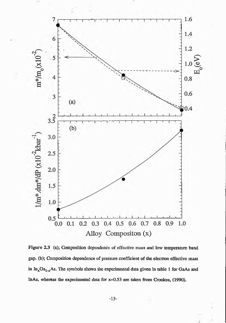
a non-linearity with respect to alloy composition as can be seen in figure 2.3.
However, there have also been many investigations into composition dependence of
the material parameters, particularly, the band gap and effective mass, in III-V ternary
and quaternary systems. A general review on the composition dependence of material
parameters has been given in a number of papers by Adachi, (1982 and 1985), and latter
in the excellent book by Adachi, (1992).
23 The Temperature Dependence Direct Band Gap E0
and Effective Mass m
The k.p. theory which is given in equation 2.2.1 applies only at zero temperature.
However, the direct band gap is expected to vary with temperature because of thermal
expansion and temperature dependent electron-phonon interactions. The effective mass
would therefore also vary with temperature due to changes in the band gap.
The temperature dependence of the band gap in a semiconductor has been given by
Varshni, (1967), as
where a and (3 are constants. Eg is called the optical or thermal band gap in the
literature. Besides the change of the band gap induced by thermal expansion of the
lattice and additional contribution arises due to the electron-phonon interactions at
temperatures where phonon density is significant. Ehrenrich, (1959), has given the
following expression for the temperature dependent dilation of the band gap
known as the effective mass band gap in the literature, [Stradling and Wood, 19970].
Equation 2.3.1 may be rewritten for Ii^Ga^As as a function of x and T if E0 is
replaced by E0(x) given in equation 2.2.4 as
where a(x) and p(x) were obtained from the two constituents GaAs and In As using the
linear interpolation method. However, a similar calculation was also carried out by Paul
et al., (1991), for InxGaj_xAs. They proposed an empirical expression as
2.3.1
2.3.2
where K is the compressibility and (OEq/OP) is the pressure coefficient of E0. E*g is
2.3.3
E g ( x , T ) = E 0 ( G a A s ) -a ( G a A s ) T 2 T + P ( G a A s )
+ [ E 0 ( I n A s ) -a ( I n A s ) T 2 T + P ( I n A s )
- E 0 ( G a A s )
+ f t ( G a A s ) T 2 T + P ( G a A s )
] x - 0 . 4 7 5 x ( 1 - x ) 2 . 3 . 4
The temperature dependent band gap calculated using equation 2.3.4 is found to give
values in close agreement with the available experimental data, [Adachi, 1992 and Paul
et al., 1991].
As mentioned previously the effective mass varies with temperature since the band
gap changes with temperature. The temperature dependent effective mass for InxGa1.xAs
can now be calculated using equation 2.2.1 (k.j> theory) with E0 replaced by Eg(x,T). In
this calculation we assumed that the momentum matrix element Ep and the valence band
spin-orbit splitting A0 were independent of temperature. This assumption is also used by
Shantharama et al., (1984), and Stradling and Wood, (1970).
Stradling and Wood, (1970), also studied the temperature dependence of the effective
mass in InAs, GaAs and InSb using the magnetophonon resonance effect. They
compared their observed results with the calculated ones from the optical band gap and
the effective mass band gap. It was found that the observed changes for GaAs and InAs
are greater than that predicted from the effective mass band gap but less than that
predicted from the optical band gap. However, they found that the observed change is
in good agreement with the predicted one from the effective mass band gap for InSb.
2.4 Pressure Dependence Band Gap and Effective Mass
The application of hydrostatic pressure does not change the crystal symmetry, but
- 1 1 -
decreases crystal volume and hence reduces the lattice constant leading to shifts in
energy. This causes the band gap to change. The direct band gap E0 increases with
pressure. The band gap between the F maximum and the L minimum E ^ increases
while the band gap between the F maximum and the X minimum Epx tends to decrease
slowly because the valence band broadens.
The pressure dependence of the direct band gap is commonly given in terms of linear
(a) and non-linear (b) pressure coefficients as
E g ( P ) = E 0 ( 0 ) + a P + b P 2 2 . 4 . 1
where P is the hydrostatic pressure. The calculated linear and non-linear pressure
coefficients, a and b, agree very well with published experimental data, [Adachi, 1992].
However, the non-linear coefficient term is only important if measurements are taken at
P>10 kbar, [People et al., 1988].
Lambkin et al., (1988), measured the pressure coefficient dE^dP for In 53Ga 47As by
photoluminescence in a diamond anvil cell between 300 and 80K. They found that
dE^dP is independent of temperature between 300 and 80K. The composition
dependence of the pressure coefficient dE^dP for In1_xGaxAsyP1_y has been studied by
Hayes et al., (1982). They observed that dE^dP increased almost linearly with increasing
A s content. No detailed reports have been published on the pressure dependence
of band gap and the effective mass in the In^Ga^As/GaAs alloy system. However, in
our calculation we assume that the pressure coefficient dE^dP can be calculated by
interpolation from the end-point binary experimental data.
From equation 2.2.1 it can be clearly seen that increasing pressure increases the
effective mass because the band gap increases with pressure. The pressure dependence
>
Alloy Compositon (x)
Figure 2.3 (a); Composition dependence of effective mass and low temperature band
gap. (b); Composition dependence of pressure coefficient of the electron effective mass
in In^Ga^yAs. The symbols shows the experimental data given in table 1 for GaAs and
InAs, whereas the experimental data for x=0.53 are taken from Crookes, (1990).
-13-
of effective mass could be calculated by accounting for the increase in the band gap with pressure using equation 2.2.1. However, in our calculations we used pressure dependence of the effective mass l/m*.dm*/dP to be that given in figure 2.3 which is interpolated from the binary end-points.
2.5 The Effect of Impurities on the Band Structure
Up until now we have considered a perfect crystal, but this is not the real situation, since all semiconductors have a number of alien atoms. These are sometimes introduced intentionally to provide one type of free carrier of the required concentration so that materials can be classified as lightly, moderately and heavily doped materials.
In the energy level-scheme, the alien atom introduces allowed levels in the band gap. Such levels can normally be described as "shallow" or "deep". These levels are separated by the ionization energy; from the conduction band for donor atoms (where the resulting level is called the donor level) and from the valance band for acceptor atoms (where the resulting level is called the acceptor level). An important problem considered here is how the pressure and temperature effect the position and occupation of such impurity levels.
The ionization energy of a shallow impurity level, which is the impurity ionization energy (Ed), being very small compared with the band gap, may be worked out using the Bohr theory of the hydrogen atom. The ionization energy for the hydrogen atom is given as
ElB=m° 3 2 * * ^ V 2 • 5 ' 1
where eG is the permittivity of free space. The ionization energy for donor levels can be written in terms of the ionization energy of hydrogen atom as
2 - 5 - 2
It is expected that the shallow levels will not show a large "trap-out" when the pressure is increased since the changes in Ed, due to changes in m and es, are small compared to kT. A similar approximation for the acceptor level can be made.
In extrinsic materials, when the sample is in thermal equilibrium, the temperature dependence of the carrier concentration due to the presence of one type of shallow donor impurity is given, [Stillman and Wolfe et al., 1976], as
=JLexp ( - D - ) 2.5.3Nd-Na-n ga K kT
where Nd is the donor impurity concentration, Na is the acceptor impurity concentration, Nc is the effective density of states of the conduction band, and gd is the spin degeneracy of the donor level. The ionization energy given by equation 2.5.2 is only strictly applicable for very low impurity concentrations. At higher impurity concentrations the activation energy Ed is reduced by the screening and increased overlap between impurity wave functions.
Lattice defects, both crystal imperfections and impurities, can also introduce deep energy levels, where the impurity ionization energy (Ej) is large compared to that of the shallow levels, and is often closer to the middle of the band gap.Such levels may have a strong influence on the electronic properties of semiconductors even at high temperatures since they can act as carrier traps, scattering and recombination centres.
Unlike shallow levels a deep impurity level is not derived from the nearest band edge state. Indeed, it is found that a description of deep level states in term of the states of host crystal can not be made without considering a large number of bands. Recently, Ledebo and Ridley, (1982), have proposed that the deep levels are largely tied to the vacuum energy level and are independent of the host lattice. For these reasons the deep levels are thought to be relatively unperturbed by the movement of the nearest band edge by pressure. So that we expect that the absolute energy positions of such levels approximately remain constant with pressure.
2.6 Material Properties and More Material Parameters
A number of material parameters, structural and energy band-structure related parameters, have been discussed so far. In this section we discuss the elastic, lattice vibrational, dielectric and piezoelectricity related parameters that appear in the scattering mechanisms discussed in the next chapter.
Elastic constants (C}. Ct): The elastic constants of III-V compounds have been measured by Gerlich, (1963), (for InAs) and Bateman et al., (1959), (for GaAs). Recently Adachi, (1985), has shown that the linear interpolation scheme was very successful to estimate the elastic constants for the AlxGala.xAs alloy system.
Like other workers we assumed that the elastic constants are independent of temperature. The pressure coefficients of the elastic constants for GaAs have been measured by McSkimin et al., (1967). We have assumed that the pressure coefficient of the averaged longitudinal elastic constant Cj for the In^Ga^As alloy system is similar
-16-
to that for GaAs.
Longitudinal sound velocity (U^: Sound velocity is related to the longitudinal elastic constant Cj by
where d is the mass density given by
M is the primitive cell mass and Q is the volume of the primitive cell. The temperature dependence of sound velocity can be calculated by considering the temperature dependence of d which arises through the thermal expansion coefficient. The pressure dependence of can also be calculated by considering the changes in Cj and d with pressure, due to material compressibility.
Deformation potential: The deformation potential is an important parameter for determining electron mobility limited by acoustic and non-polar scattering mechanisms in III-V compounds. The deformation potential is defined as the electronic energy shift due to uniaxial strain effects on the band structure. In this case, the scattering of electrons is primarily due to the acoustic deformation potential. The band edge shift caused by these can be described for direct gap materials by considering only the linear term (dilation term) in the strain, [Ehrenrich, 1960], and this is given by
E 2.5.5AC K dP
-17-
where K is the compressibility. In the case of Ii^Ga^As we use the values obtained from the linear interpolation scheme using the GaAs value obtained by Lancefield et al.,(1987) and the InAs value obtained by Rode, (1971). We have also assumed that its temperature dependence is similar to that for GaAs, and that the pressure dependence can be neglected [Lancefield, 1987]. Both the value of the deformation potential and its pressure dependence could be calculated from equation 2.5.5. However, it has been fond by many workers that equation 2.5.5 does not give good agreement with experiments made as a function of temperature. For this reason EAC has been used an adjustable parameter in the past [Adachi, 1992].
Piezoelectricity: The HI-V compounds crystallising in the zinc-blende structure are the simplest crystals lacking a centre of symmetry and, hence, are capable of exhibiting piezoelectricity and related effects. The piezoelectric constant (Pm) for zinc-blende structures is given by Rode, (1971), as
-r-,2 2 r 12 .1 6 1 1 o r- C3 5 i; 2 -5 - 6
where es is the low frequency dielectric constant, Ct is the averaged transverse elastic constant, and e14 is the piezoelectric coefficient.
The composition dependence of the piezoelectric constant Pm could be calculated using equation 2.5.6 by considering the composition dependence of Cj, Ct, e14 and es. We prefer to calculate the composition dependence of Pm by using the end binary values of Prn itself in the interpolation because it requires less assumptions than other way. However, both calculations give a similar result.
Static and high frequency dielectric constants: The values of the static (cs) and high frequency (eoo) dielectric constants of GaAs and InAs are given in table 2.1. Adachi,(1982), has studied trends in the dielectric constants of III-V compounds and related ternary and quaternary alloy systems, and concluded the constants can be calculated by the use of the simple linear interpolation method.
However, if no measured values of temperature and pressure coefficients of the dielectric constants are available then the Lyddane-Sachs-Teller (LST) relationship, [Samara, 1983], for es and the relationship c^n2 (n:refractive index) for can be used to estimate the related coefficients.
Phonon energies: The polar optical phonon scattering process is the dominant scattering mechanism at high temperatures in In^Ga^As. We need a knowledge of the optical phonon energies to evaluate this scattering mechanism.
The phonon dispersion relations for III-V compounds have been studied by several authors, [Hass et al., 1962, Palik et al., 1968 and Waugh et al., 1963]. IH-V compounds crystallizing in the zinc-blende structure exhibit similar phonon dispersion relations. The optical phonon branches exhibit the small wave-vector dependence near the zone centre while the acoustic branches exhibit the approximately linear dependence on wave vector k. In this work we assume the optical vibrational frequency is independent of wave vector k.
The optical phonon energies for GaAs and InAs are given in the table 2.1. For Ir^Ga^As the simple linear interpolation method was used to estimate the composition dependency.
Alloy scattering Potential (ALT): In alloy semiconductors, such as InxGa1_xAs, the electrons may "feel" the potential fluctuations due to the compositional disorder. This effect gives rise to an additional scattering mechanism in alloy semiconductors. In the literature the values of the alloy scattering potential for InxGa1.xAs are considered to be the band gap difference, [Berolo et al., 1973], the difference electron affinity, [Harrison and Hauser, 1976], and the electronegativity theory, [Littlejohn, 1978]. The electronegativity theory, [Littlejohn, 1978], predicts that AU varies from 0.55 to 0.51 as x changes from 0 to 1. Chattopadhyay et al., (1981), have used an x-independent value of 1.15 eV. In contrast, in our calculation AU is an x-dependent parameter, [Adachi, 1985], given by
A U = U [ x ( 1 - x ) ] 1/2 2 . 5 . 7
The constant U is taken as 1.06 eV from the electronegativity theory assuming AU has a maximum value of 0.53 eV at x=0.5. For Iuq 53GaQ 47As the value of alloy scattering potential calculated from the interpolation has been found in good agreement with the experimentally obtained values [Adachi, 1992).
T a b le 2.1 M a te ria l p a ra m e te rs
Parameters
a(A )
p(g/cm3)
E0(eV)(T=4K)
E ^ e V )
E n J e V )
^ ftm eV /k b a r)dP
A0(eV)
aClO ^eV/K)
P(K)
U ^ K ^ cm /s)
Ec(eV)
K(10“3/kbar)
m*mG
5.653
5.307
1.52
2.015
I.45
I I .1
0.341
5.405
204
5.102
6.74b
1.34
G aA s1
0.067
“21™
6.08a
5.667b
0.41°
2.1d
1.77d
10.0e
0.38f
6.0®
500®
4.197
6.76b
1.727b
In A s
0.023°
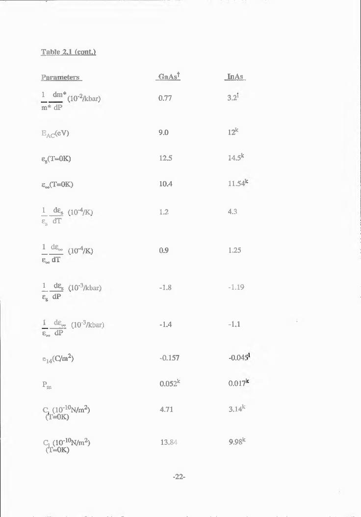
T a b le 2.1 (cont.)
Parameters GaAs4 InAs
1 dm*fl0'2/kbar> m* dP
0.77 3.2‘
EAC(eV) 9.0 12k
es(T=OK) 12.5 14.5k
eJT=0K) 10.4 11.54*
1 d®, flO^/Kt es dT
1.2 4.3
1 de~ ao^/Ki e„dT
0.9 1.25
1 des a0'3/kbar> es dP
1 ►—1
bo -1.19
4 d®™ (iO"3/kbar) 6 . dP
-1.4 -1.1
e14(C/m2) -0.157 -0.04:
Pm 0.052k 0.0171
C. (10'10N/m2) (T=OK)
4.71 3.14k
C, (10'10N/m2) (T=OK)
13.84
-22-
9.98k
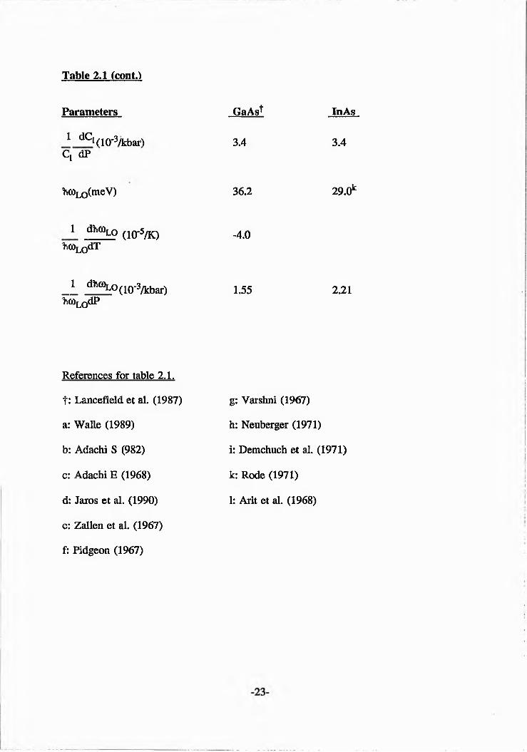
T ab le 2.1 (cont.)
Parameters
1 dCl(lQ-3/kbar'l Cj dP
'hwLO(meV)
1 d t o LQ ( 10'5/K )friO>LodT
_ i ± ^ ± °(10-3/kbar) ta>LOdP
References for table 2.1.
f : Lancefield et al. (1987)
a: Walle (1989)
b: Adachi S (982)
c: Adachi E (1968)
d: Jaios et al. (1990)
e: Zallen et al. (1967)
f: Pidgeon (1967)
3.4 3.4
36.2 29.0*
-4.0
1.55 2.21
GaAs^ B i As
g: Varshni (1967)
h: Neuberger (1971)
i: Demchuch et al. (1971)
k: Rode (1971)
1: Arlt et al. (1968)
C h a p t e r 3
Low Field Transport Theory
3.1 Introduction
The theory of electron transport is concerned with the evaluation of transport coefficients under the influence of an electric field with or without a magnetic field. In this chapter, the Boltzmann equation is described with two solution methods. These are the relaxation time approximation and the iterative solutions.
In particular, we discuss some important scattering mechanisms in terms of the partial mobilities. The importance of partial mobilities is emphasized in the temperature and effective mass dependence of the mobility.
3 .2 E le c t r o n S c a t te r in g
An electron moving in a perfectly periodic potential field behaves as a free electron; the periodic potential effectively only changes the effective mass of the electron. However, the assumption of a perfectly periodicity in real crystals is invalid. The periodic potential is modified in two ways. Although the arrangement of atoms in a perfect crystal is periodic, the atoms move all the time about the equilibrium positions due to their thermal vibration at a finite temperature. Hence the vibration of atoms
-24-
Secondly, complete purification is not technically possible. There are a number of alien atoms embedded in all semiconductors with the result that the periodicity of the potential is changed by these impurity atoms. Imperfections in the crystal structure also alter the periodicity of the potential. In addition the presence of other electrons also affects the potential in their vicinity.
Consequently, an electron in a semiconductor cannot execute long-range motion without changing state. Therefore, the electron has to change its state when it arrives in the vicinity of an impurity atom, another electron or crystal imperfection, and also by interacting with the thermally disturbed lattice. These changes of state are referred to as collision or scattering processes.
The scattering mechanisms can be divided into two groups; the intrinsic and extrinsic. The intrinsic mechanism involves the thermal effects. The extrinsic mechanisms involve the effects of alien atoms and imperfections in the lattice.
3.3 The Boltzmann Equation
3.3.1 Introduction to the Boltzmann Equation
The theoretical value of mobility of a semiconductor specimen can be obtained by solving the Boltzmann equation which is derived from the more general Liouville equation. However, there are a number of other methods of obtaining the mobility in a semiconductor, [Moore, 1967].
Although the Liouville equation gives a complete description of the evaluation of the
affects the periodic nature of the potential.
-25-
system in time under the action of the forces, it is almost impossible to calculate transport coefficients using this equation. The Boltzmann equation is preferred in the study of transport processes.
A number of texts of the derivation of the Boltzmann equation are available, [Nag, 1980], and the equation is given here as
§ § = ( f 3 . 3 . !
where 3f/9t is the rate of change of f due to scattering eventsTo illustrate the method of solving of the transport equation for equilibrium conditionsand homogeneous sample, equation 3.3.1 can be reduced to
( ) -Vfcf = ( -q£ ) coi l 3 . 3 . 2
The problem then, is to describe the collision term on the right-hand side of this equation.
The collision term is derived by making several assumptions. Firstly, the probability of a transition (differential scattering rate) from an initial state k to final state K depends only on k and 1U and does not depend on the position of the particles and that the duration of collision is negligible. Therefore the scattering rates can be derived in the Bom approximation. This is valid for short range scattering potentials and when the carrier energy or thermal energy of the electron is high. Under these conditions the number of electrons transferred from k to K can be determined by the distribution of the electrons alone.
Secondly, the individual scattering mechanisms are independent of one another, so that the total scattering rate is the sum of the component scattering rates. The
-26-
expressions of scattering rate of the various scattering mechanisms and the collision term have been given by Nag, (1980). The collision term is
<|£>coii=-^f Cftl-fiJS-fiCl-fJSjdk' 3.3.3k
wheref = f(Lk,t) , fx = ffck'.t)S=S(kJc'), S^SQcJl)
S and Sj are total differential scattering rates for all the collisions. Equation 3.3.3 which is known as the collision integral makes the Boltzmann equation 3.3.2 an integro-differential equation which cannot be solved by analytical methods.
We shall discuss two approximate methods to solve the Boltzmann equation in the next section.
3.3.2 Relaxation Time Approximation
In the relaxation time approximation it is assumed that the distribution function of the elections has been disturbed and after a time constant 'c(k), which is known as relaxation time, the perturbed electron distribution will return to the steady state distribution. Hence the collision term in equation 3.3.2 is reduced to
(j£) — £-£° 3.3.46 t x (k)
This approximation is only valid for elastic scattering mechanisms. In the presence of several scattering mechanisms, the total relaxation time is given by
-27-
.. . 1 = y * 1 3 3 5x ( k ) x ± ( k )
where Tj(k) is relaxation time of each of the individual scattering processes.We can now calculate the Drift mobility by applying an electric field F to the
homogeneous semiconductor sample. In the steady state, equation 3.3.2 reduces to
where f0 is the equilibrium function. This equation yields, for the perturbation of the electron’s distribution function g
_ - e F T ( k ) d f Q 3 . 3 . 79 %0k
After several steps, for a non-degenerate semiconductor, the current density is obtained as
< t > F 3 .3 . 8m*
wherer X ( E ) E 3 / 2 e x p ( - E / k T ) d E
= 3 .3 .9E 3 / 2 e x p ( - E / k T ) d E
Jo
Finally,the Drift mobility is given, [Look, 1989], as
n = J L < t > 3 .3 .10m*
Similarly, when applying both electric and magnetic fields the Boltzmann equation is written as
-28-
[E + -J v kE xfi] . Vkf = -^ -^ ° 3 . 3 . 1 1n n t
Hence, the Hall mobility is then given, in the limit |B |—>0, by
3.3 .12m* <t >
It is noticeable that the Drift and Hall mobilities are not the same. The Hall mobility differs from the Drift mobility if x is dependent on energy. If x is independent of energy, the Drift and Hall mobilities are identical for spherical constant energy surfaces, but not for non-spherical constant energy surfaces.
In the presence of several scattering mechanisms, if the individual relaxation times, x̂ kys, have the same energy dependence, the mobility is then given by
— = y\ — 3 .3 .13H n ±
This approximation is known as Matthiessen’s rule and is satisfied in the degenerate limit. Although the majority of scattering processes may be analyzed by applying this method because it allows the scattering mechanisms to be investigated independently, this approximate method is only valid for elastic scattering. Furthermore, polar phonon scattering which is inelastic is the dominant scattering mechanism at room temperature in m-V semiconductors. Further discussion on the application of the relaxation approximation is given by Look, (1989).
In the next section we will describe an iterative solution of the Boltzmann equation which more accurately describes the various scattering mechanisms because it includes the inelastic and elastic rates.
-29-
3.3.3 I te ra tiv e Solu tion o f th e B o ltzm ann E q u a tio n
An iterative solution of the Boltzmann equation can be used to calculate the electron mobility. The technique was initially suggested by Rode, (1970), and has been developed in a number of papers by Rode, (1971, 1973, 1975), and Rode and Knight, (1971). It allows the inclusion of Fermi statistics, energy band non-parabolicity, electron wave function admixture, and the various scattering mechanisms are combined at the matrix element level, i.e., each scattering mechanism is independent of others.
Rode has shown that the technique based on manipulating the Boltzmann Equation into a linear finite-difference equation reduces to solving the following two coupled differential equations, for which gi+1 and hi+1 are solutions of the (i+l)* iteration.
9 i + l
S l ( g ± ) - e ( F A ) . ( - ^ J + p S K h i ) 3 . 3 . 1 4
s 0 ( i + p 2)
and
SI(hi)-(PF/!h) { - * £ ) +31^) 3 . 3 . 1 5
s 0 ( i + p 2)
where
m*d
and
-30-
S 0 = ( S I 0+ v e l )
SI and SI0 are the inelastic scattering rate into and out of the volume element dk and 0)el is the sum of all elastic rates. The expressions of differential rates for this formalism have been given by Rode, (1975).
This method of iteration has been found to be convergent and the results converge to within 1% in between four and six iterations. As |B|—>0 it can be seen that equations 3.3.14 and 3.3.15 decouple and can be solved independently. Secondly, if there is no inelastic scattering mechanism it can be also shown that
e F t ( k ) d f 0 3 . 3 . 1 6a b S k
where the relaxation time is given by
( 1 _ x ) S 6i d k /= v „i
where x is the cosine of the angle between k and U, oel is the sum of the elastic scattering rates and Sel is called the elastic scattering rate. Equation 3.3.16 is the perturbation of the electron’s distribution function which is the same function used into relaxation time approximation.
Subject to the above limitations, the ISBE is reduced to the relaxation time approximation.
-31-
3.4 Scattering Mechanisms
3.4.1 Deformation Potential Scattering
Acoustic phonons produce a perturbing potential in two ways. In the first of these the acoustic vibrations induce changes in the lattice spacing, which change the band gap from point to point. The potential so produced due to the deformation of the crystal is called the deformation potential and the scattering of carriers through the deformation potential is called the deformation potential scattering. The Drift mobility for this mechanism is given by Bardeen and Shockley, (1950), as
2 ( 2 n ) 1/ 2V 1p U J e . . . . . . . , . .Bag- ------------ - t— —— T 3/2Itl* 5/2 3 . 4 . 1
oV 3/ 2P 2 J k b ^ac
where p is the mass density, Uj is the average longitudinal sound velocity and EAC is the acoustic deformation potential.
3.4.2 Piezoelectric Potential Scattering
The second kind of perturbing potential is produced by the acoustic vibrations through the Piezoelectric effect if the atoms are partially ionized. Both longitudinal and transverse phonons can scatter electrons by this mechanism, but the former dominates. The resulting mobility for this mechanism is given by Zook, (1964), as
_ 1 . 7 4 x 1 0 -Meg 1 / 2 . - 3 / 2 3 . 4 . 2•*“ e ^ U / C ^ / C , . )
where e14 is the piezoelectric constant, and where Ct and Cj are the transverse and longitudinal elastic constants respectively. This mechanism is significant in all compound semiconductors, especially in m-V semiconductors and particularly at low temperatures.
3.4.3 Polar Optical Phonon Scattering
The perturbed potentials produced by the optical vibrations also scatter electrons in two distinct ways. The first of these is that due to the dipole moments formed by the interaction of the ionic charge on the atoms with the optic vibrations. Transverse optical phonons do not interact with the atoms to produce a dipole, hence they do not scatter.
The mobility for this mechanism was initially described by Ehrenreich, (1959), and developed by Fortini et al., (1970), and is given here as
_ 16Tie0 (2rckB) G ( z ) [ e x p ( z ) - 1 ] 1/2 . .3,2 3 4 3Pp0 3 e u 1 ( l / e . - l / G a)
where C0j is the longitudinal polar optical phonon frequency and z =̂ 0̂ /kRT, and G(z) is the effect of electron screening on the scattering by polar phonon and has been given for pure materials, [Ehrenrich, 1959 and Fortini et al., 1970]. However, the free carrier screening has been incorporated into the differential scattering rate for polar optical phonon given by Rode, (1975).
This mechanism is the most important scattering mechanism for pure materials from room temperature to liquid-nitrogen temperature. It is noted that this mechanism is inelastic and the relaxation time solution to the Boltzmann equation is not viable for this mechanism, since 1 becomes a function of the perturbation strength itself and not just
-33-
of the electron’s energy. However, it is possible to use the iterative solution of Boltzmann equation discussed previously.
3.4.4 Ionized Impurity Scattering
3.4.4.1 Introduction
As mentioned previously there are alien atoms in all semiconductors even though they may have been nominally undoped. These are also sometimes introduced intentionally to provide one type of free carrier of the required concentration.
In relatively pure materials, the impurity atoms are mostly neutral at very low temperatures (near liquid-helium temperature). The impurity atoms become ionized with increasing temperature (liquid nitrogen) and so the ionized impurity scattering becomes dominant. The importance of this mechanism increases as the temperature is increased from very low values to near liquid nitrogen. But this mechanism may be important for the materials with a high concentration of impurity atoms even at room temperature.
3.4.4.2 Scattering bv Random Impurity Distributions
The usual description of ionized impurity scattering is based on the fact that the potential associated with the impurity atoms is different from that of the atoms in the host crystal. The initial formulation for this mechanism was given by Conwell and Weisskopf, (1950), and they modelled the impurity potential by a Coulomb potential. In this approach the relaxation time diverges for small angle scattering by introducing
an arbitrary cut-off distance. This arbitrary cut-off distance can be removed by the inclusion of screening effects on the scattering potential. Dingle’s approach, [Dingle, 1955], included screening effects by electrons on the scattering potential. However, in our calculations we use the Brooks-Hening theory of ionized impurity scattering, [Brooks, 1955], which includes screening by both electrons and neighbouring impurities. The resulting mobility is then given as
128(2x) 1/2esk|/2 ,,, . , b-----NlZse3 ---T3/2m*1/2[ln(l+b) _Y5g-1] 1 3.4.4
where b=4kB /ps2 and
„ _ e . nF.1/2(n) + (ND-NA-n) (NA+n) ° e0e8kBT F1/2(n) N„
Fj(ri) is a Fermi integral of order j, where ft is the reduced Fermi energy. For non-degenerate materials these integrals cancel out. They have been tabulated by Blakemore, (1987). Nj is the concentration of ionized impurities and Z is the charge on the impurity in units of e.
The Brooks-Herring theory, given in equation 3.4.4, is based on the Bom approximation. Therefore, the validity of the Brooks-Herring theory is dependent on the validity of the Bom approximation, which is generally given as b»l. This implies nondegeneracy. If the Bom approximation is not valid, then the phase shift analysis, [Meyer and Bartoli, 1981], may be used to calculate the mobility.
Another problem is the loss of free-carrier screening which may arise at low temperatures in high purity material, or at higher temperatures in semi-insulating and highly compensated materials. When the screening effects are small or no screening is
present, then the scattering cross-section diverges for low scattering angels. However, the Conwell and Weiskopf approximation partially solved this problem in a rather arbitrary manner by cutting off the potential, so that in this approximation collisions were only allowed for electrons that approached within Nf 1/3/2, half impurity separation.
One of the assumptions made in the Brooks-Herring theory is that impurities are distributed randomly, and an electron is scattered by the potential of a single impurity. If the scattering centres are close together, multiple scattering effects must be important for highly doped semiconductors. A more complete discussion of this problem is given by Yanchev et al., (1979), and Meyer and Bartoli, (1985).
Further discussion on the validity of equation 3.4.4 and the refinements to the Brooks-Herring theory are available from a number of papers, [Cattopadhyay and Queisser, 1981, Lancefield et al., 1987, Look, 1989].
3.4.5 Neutral Impurity Scattering
As mentioned in the previous section, the donor impurity atoms are mostly neutral at low temperatures. Hence the electron scattering from neutral impurities may be significant at low temperatures where carrier freeze-out occurs or at high impurity concentrations. For this mechanism several formalisms have been discussed by Look, (1989). The formalism of Erginsoy, (1950), gives the mobility limited by this mechanism as
H„=------ e3l“ * — 3 . 4 . 580NN7te0eo».3
where Nn is the density of neutral impurities.
-36-
3.4.6 Allov Scattering
The ternary compounds exhibit an additional scattering mechanism. This arises from
the random arrangement of the constituent A and B atoms among the C atoms where the
ternary composition is of the form AXB^XC. The random arrangement o f atoms gives
the crystal potential a random component leading to the alloy scattering. The mobility
limited by alloy scattering for the alloy Ax B1-x C has been given by Littlejohn et al.,
(1978), as
n = _ _ J _______________________________________________ T - i / 2 in » - 5 / 2 3 4 6
37t0 [x (! -x )3 (Au) 2S (a ) k®/2
where S(a) is an energy-dependent parameter which describes the effect of ordering on
the scattering rate. In general 0<S<1, where S=0 for a perfectly ordered ternary (super
lattice) and S=1 for a completely random alloy. AU is the alloy scattering potential,
discussed in chapter 2, and x is the mole fraction of element A.
3 . 5 I m p u r i t y C o n d u c t i o n a n d t h e H o p p i n g P r o c e s s
At sufficiently low temperatures, the transport effects in doped semiconductors are
not due to free carriers in the conduction band. The transport occurs between impurity
states in the energy gap without entering the conduction band. This type of transport is
known as impurity band conduction.
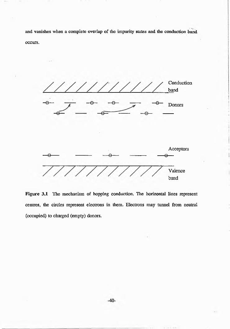
In the impurity band there are at least two possible mechanisms of conduction
depending on the degree of overlap between impurity centres; these are the thermally-
activated hopping and metallic conduction. However, for relatively pure semiconductors
at low temperatures the electrons are strongly bound to their impurities (i.e. they are
strongly localized) and the overlap between impurity centres is negligible.
Thermally-activated hopping: At low impurity concentrations (where the overlap
between impurity centres is small) in the presence of acceptors, impurity conduction is
able to occur among the donors of n-type semiconductors. As a result of the perturbed
donor energy levels due to the random field of acceptors, the tunnelling takes place
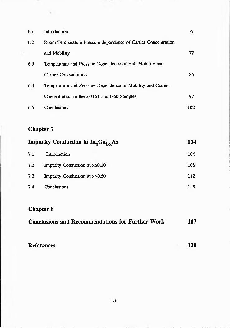
from an occupied donor to the nearest unoccupied one with the energy 83 as shown in
figure 3.1. The electron must exchange energy with a phonon each time it moves. This
process is called phonon-assisted or thermally-activated hopping conduction. This kind
of hopping was first described by Miller and Abrahams, (1960). In their theory, the
electron-phonon interaction through the deformation potential is assumed to be
responsible for this kind of hopping conduction. Their result can be written as
p=p3e x p [1J | ] 3 . 5 . 1
where e . the is activation energy and given by Butcher, (1980), as
p 2n 1/3e 3= 0 .9 9 -a__ L _ < l - 0 . 3 k 1 /4) 3 . 5 . 2
3 4tte0e s
for low compensation (k<0.4), and
2vrl/3„ _ f 2JI, 1/3 e WD / • ,_>)-1/3 3 . 5 . 33 lT j 4tie0e;' '
for high compensation (k>0.4). The resistivity p3 could be calculated for any
semiconductor using the Miller-Abrahams theory. However, later using the percolation
theory, Shldovskii, (1973), has given a more general formula,
p3=p0exp[ ” ] 3.5.4N p a B
where ND is the donor concentration, aB is the effective Bohr radius, a is a constant
which is related to percolation radius. p0 is given by Shklovskii and Efros, (1984), as
Po=Ca|(NS/3a B) 6 3 . 5 . 5
where 8=0-0.4. The quantity C depends on the nature of the electron-phonon interaction.
For the deformation potential interaction, Kahleit et al., (1976), have deduced from the
Miller-Abrahams theory that C is given by,
c = 9£ Y d e £ 1 3 5 6e 'E l
where Ec is the deformation potential constant.
M etallic conduction: At high impurity concentrations where the overlap between
impurity centres is large the thermally-activated hopping conduction is no longer
significant. The conduction in the impurity band is of a metallic character with the
electrons behaving like a degenerate electron gas. These have been discussed extensively
by Mott, (1990).
The transition from one mechanism to the other depends on the ratio of the average
distance between donor impurities rD to the hydrogenic-like Bohr radius of donors aB,
[Mott and Twose, 1961]. The transition occurs for rQ/aB~3.6. This suggests that for
ND1/3aB>0.25 the conduction is the metallic like. The activation energy 83 tends to zero
-39-
and vanishes when a complete overlap of the impurity states and the conduction band
occurs.
Conductionband
Donors
Acceptorse —— ------ — — ©— - —— — _ e _
Valence band
Figure 3.1 The mechanism of hopping conduction. The horizontal lines represent
centres, the circles represent electrons in them. Electrons may tunnel from neutral
(occupied) to charged (empty) donors.
C h a p t e r 4
A p p a r a t u s a n d E x p e r i m e n t a l T e c h n i q u e s
4 .1 I n t r o d u c t i o n
The electrical transport measurements for InxGaj.xAs reported in this thesis were made
on clover leaf samples using the van der Pauw technique, [van der Pauw, 1958], The
clover leaf samples were prepared by photolithographically defined etching. The
temperature measurements were made in a standard cryostat system. The high pressure
measurements as a function of temperature between 4.2 and 300K have been made using
the high pressure-temperature measurement system developed by Lambkin et al., (1988),
at Surrey. This system is based on a piston and cylinder high pressure system with may
be placed within the 2 cm bore of a standard cryostat system.
4 . 2 S a m p l e P r e p a r a t i o n
4.2.1 Clover Leaf Preparation bv Etching
Clover leaf samples were prepared by defining photolithographically the area to be
etched. The sample was cleaned by boiling it for ten minutes in methanol and then
trichloroethylene, and in an iso-propyl alcohol (propane) bath for 30 minutes to remove
-41-
Three layer's of Shipley AZ 1350H positive photoresist were applied to the sample’s
surface and the sample spun at 800 r.p.m. for 1 minute. This produces a uniform layer
of photoresist, approximately 0.7 pm thick, on the sample surface. The sample was then
pre-baked for 20 minutes at 80°C to harden the photoresist. The negative mask of the
clover leaf pattern was placed over the sample surface and then exposed to ultraviolet
light for 15 minutes. The photoresist was then developed in a 100:1 mixture of E y j and
NaOH and the unexposed photoresist was then washed away. The sample was then post
baked at 120°C for 30 minutes to further harden the remaining photoresist.
The epitaxial layer was etched away in a solution of H2S 0 4, H20 2 and H20 in the
ratio 1:125:1, which at the room-temperature gives an etch rate o f approximately 1
pm/minute. Finally, the sample was washed in deionized water and the photoresist mask
was then removed by placing the sample in acetone for a short while.
4.2.2 Contact Fabrication
Ohmic contacts were made by alloying indium or tin dots onto the sample. Initially,
the sample was cleaned as previously described. The wire leads were then placed on the
indium or tin dots located at the edges of four clover leaves and then alloyed into the
sample in a hydrogen/nitrogen atmosphere, at a temperature just greater than the melting
point of the contacts, for approximately 2 minutes.
any other contaminates and deposits from the sample surface.
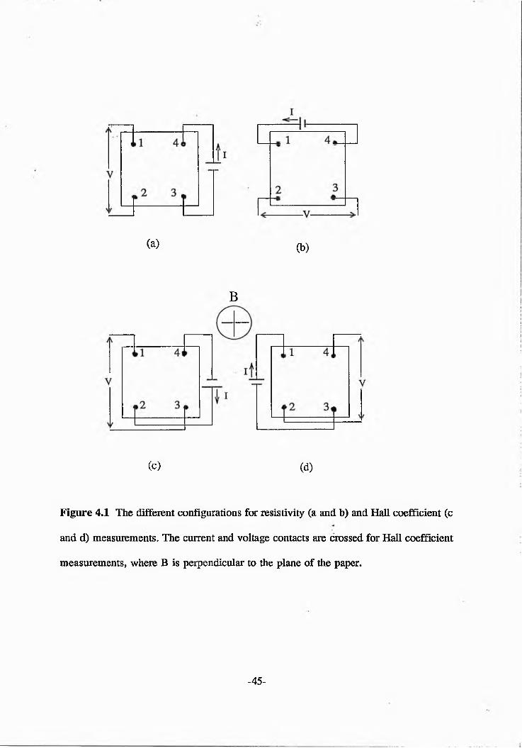
4 . 3 R e s i s t i v i t y a n d H a l l c o e f f i c i e n t M e a s u r e m e n t s
The resistivity and Hall coefficient measurements of InxGa1.xAs samples were
measured using the van der Pauw technique, [van der Pauw, 1958]. This technique only
requires four contacts on the perimeter of the sample in contrast the Hall bar
configuration. However, it is necessary to make a greater number of measurements in
the van der Pauw technique than the Hall bar configuration. This requires the
interchanging of current and voltage leads as shown in figure 4.1. Basically, only four
measurements are necessary, two resistivity and two Hall voltage measurements.
However, sixteen measurements (8 resistivity and 8 Hall voltage measurements),
including reversals of the current and magnetic field, were taken to obtain maximum
accuracy and to eliminate thermally generated voltages produced by Ettingshausen,
Nemst and Righi-Leduc effects.
Recently the validity of the van der Pauw technique and the errors due to thermally
generated voltages and magnetoresistivity effects have been discussed by Look, (1989).
The van der Pauw technique is valid, if the following assumptions are satisfied; the
contacts are infinitely small, the contacts are on the periphery of the sample, the sample
is flat, homogeneous, isotropic, and free of holes, and magnetoresistivity effects are
negligible. Obviously, an infinitely small size of the contact is not possible but the errors
generated from the finite size of contacts may be minimized by using a clover leaf
shaped sample, [van der Pauw, 1958]. Inhomogeneties in the conducting region leads to
anomalous results in the mobility through the resistivity, [Wolfe et al., 1973]
The resistivity, p, is given by van der Pauw, (1958), as
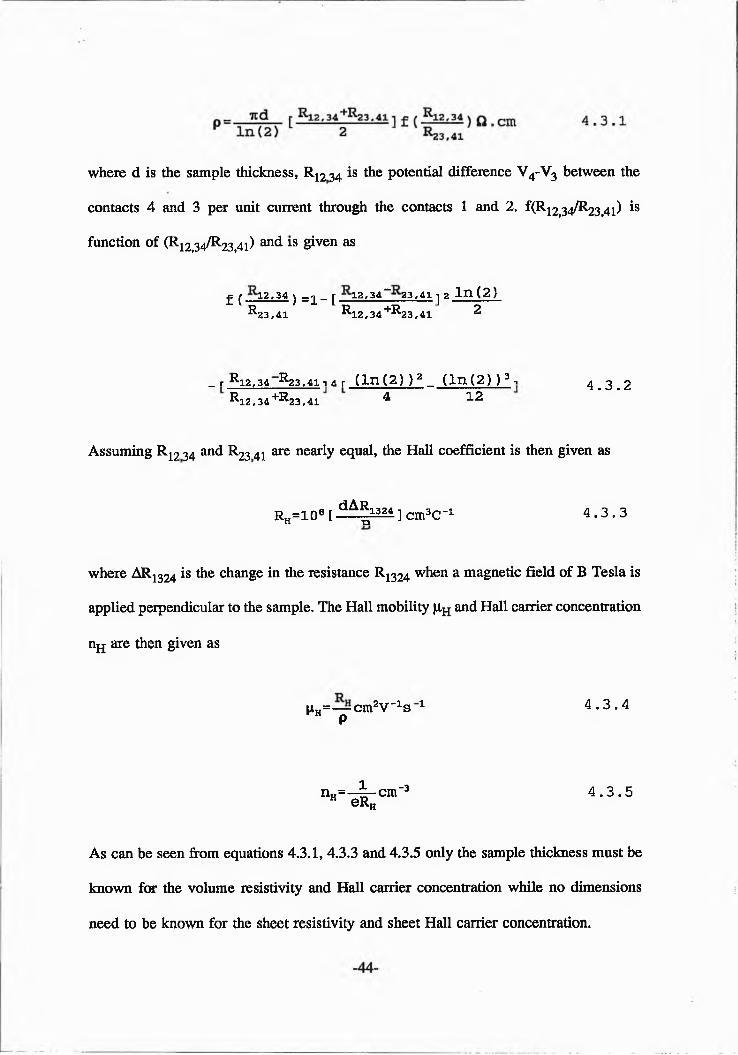
where d is the sample thickness, R12 34 is the potential difference V4-V3 between the
contacts 4 and 3 per unit current through the contacts 1 and 2. f(Ri2t34/^ 23,41) Is
function of (R12?34/̂ -23,41) and *s given as
f ( 12 '34 ) =1- [ 12,34 *" 23,41 -j 2 lrt (2)■̂ 23,41 ^12,34+ 2̂3,41 2
_ r '̂ •12,34 ^23,41-i 4 r ( l n ( 2 ) ) 2 _ ( l n ( 2 ) ) 3 n 4 . 3 . 2R12,34+I^23,41 4 12
Assuming R12 34 and R23 41 are nearly equal, the Hall coefficient is then given as
EH=l 08 [ i^ |l2 M ] cm3C-i 4 . 3 . 3
where AR1324 is the change in the resistance R1324 when a magnetic field of B Tesla is
applied perpendicular to the sample. The Hall mobility jj,h and Hall carrier concentration
nH are then given as
pH= — cm2V_1s 1 4.3.4p
nH=—̂ -cnT 3 4 . 3 . 5H eR„
As can be seen from equations 4.3.1,4.3.3 and 4.3.5 only the sample thickness must be
known for the volume resistivity and Hall carrier concentration while no dimensions
need to be known for the sheet resistivity and sheet Hall carrier concentration.
(a) (b)
B
(c) (d)
Figure 4.1 The different configurations for resistivity (a and b) and Hall coefficient (c
and d) measurements. The current and voltage contacts are crossed for Hall coefficient
measurements, where B is perpendicular to the plane of the paper.
-45-
The Hall measurement system was fully automated and was controlled by a BBC
microcomputer via an IEEE instrumentation bus. The complex switching required for the
different measurement combinations was achieved via a 3D relay box, controlled by the
BBC computer. A constant d.c. current supply was used to give currents in the range 1
pA to 10 mA. The current supply was not controlled by the computer but the current
remained constant within ±0.1% during the course of an experiment. A Keithley 196
digital multimeter with resolution of 1 pV was used to monitor the voltages. The BBC
computer’s program took six readings to check for drift and random variations. If the
standard deviation of the data was greater than the specified value, more data points
were taken until the required stability was achieved. The required switching of the
magnet was achieved via a heavy duty 10 A relays again controlled by the BBC
computer and measured by the voltage across a series resistor. As a result small
variations in magnetic field during the duration of an experiment were not significant.
4 . 4 C r y o s t a t a n d T e m p e r a t u r e C o n t r o l S y s t e m
The temperature variation of the sample in the temperature range 4.2-300K was
obtained by using an Oxford Instruments CF1200 continuous flow cryostat and a CF300
gas cooled transfer tube. The temperature of the sample was measured by a gold-iron-
chromel thermocouple mounted on the heat exchanger adjacent to the sample space. The
cold junction of the thermocouple was immersed in liquid nitrogen. The output signal
from thermocouple was sent to a programmable Oxford Instruments 3120 three term
temperature controller to set and maintain the required temperature.
The cryostat heat exchanger and the temperature controller were interfaced to the
-46-
BBC computer. This allows, using a suitable BBC program, both the thermocouple
temperature to stabilize and the sample temperature in the exchange gas to come into
equilibrium with the heater before measurements on the sample are initiated.
Temperature stabilities of ±0.2K were normally obtained. The data obtained during the
course of an experiment was stored on a floppy disc.
4 . 5 H i g h p r e s s u r e A p p a r a t u s
4.5.1 Introduction
Hall effect and resistivity measurements as a function of pressure (0-8 kbar) at the
room-temperature and as a function of temperature (4.2-300K) at the fixed pressures (~4
kbar and ~8 kbar) were made using a high pressure system developed by Lambkin et al.,
(1988), at Surrey. This system consists of a piston and cylinder apparatus developed at
the Science and Engineering Research Council (SERC) High Pressure facility at the
Standard Telecommunication Laboratories (STL), Harlow, and a high pressure cell which
is easily fitted into a standard Oxford Instruments continuous flow cryostat.
4.5.2 Piston and Cylinder Apparatus
The high pressure apparatus used to achieve pressures in the range 0-8 kbar,
consisting of a piston and cylinder, is shown schematically in figure 4.2. The cylinder
was made of hot-worked die steel and was located inside a non-load bearing steel
cylinder to confine any cylinder fracture. The cylinder was held on the die by steel
-47-
straps and was supported on the safety spacers, to prevent it rising and crushing when
the load was removed or in the event of a sudden leak.
Both the fixed and the thrust pistons were made of hardened tool steel with a
diameter of 29.25 mm. The thrust piston was longer than the fixed piston, to allow for
its necessary travel when the load was applied. The electrical feed troughs in the fixed
piston consist of conical plugs made out of hardened silver steel, which are isolated from
the piston with Vespel seals. Insulated copper wire was soldered to the plug and fed
through an axial hole in the piston. The piston was separated from the die by a backing
pad, which had a groove milled in it for the electrical leads.
The required sealing between the pistons and cylinder was achieved by using a
combination of a neoprene "O-ring" and a tapered nylon ring for measurements up to
8 kbar.
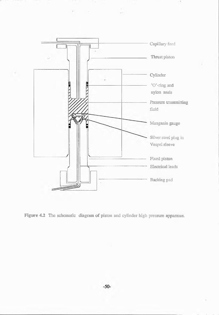
4.5.3 The Use of Three-wav Harwood Coupler and the Stub
The pressure generated in a standard piston and cylinder system described above is
fed out via a capillary feed through in the top piston. The horizontal outlet of a standard
Harwood three-way coupler is then fed by the capillary from the piston and cylinder
intensifier system as shown in figure 4.3. The straight through top outlet was fitted with
a capillary stub, into which the wires and fibre are sealed with epoxy resin and nylon
cylinder also shown in figure 4.3. The high pressure cell in the cryostat is then fed by
a capillary from the bottom down outlet of the Harwood three-way coupler.
A stub was prepared by cutting a length of a capillary approximately 7 cm long as
shown in figure 4.3. One end of capillary bore was initially drilled out to a diameter of
1.0 mm and a depth of 3.3 mm, then it was redrilled to a diameter of 1.1 mm to depth
of 1.3 mm. The stub was then cleaned in boiling methanol and trichloroethylene.
One optical fibre and five enamelled copper wires (one of them was spare), 0.07 mm
diameter and of approximately 1 m length were cut. The protective coating of fibre was
removed from a 4 cm region, starting 20 cm from one end, where the high pressure seal
was to be made. The coating is rapidly eroded by the pressure transmitting fluid. So that
failure of the stub could be a problem if this was not done. The fibre and wires were
then fed through a 3 pm hole drilled in a 1 mm nylon cylinder which was used to
provide an unsupported area. The fibre and wires were then placed into the stub. A
suitable jig was used to locate seal the nylon in the 1.1 mm guidance hole of the stub,
after which it was pushed down onto the stub in the capillary bore.
Next the standard capillary bore of the stub was filled with the epoxy resin. A low
viscosity Araldite resin (MY750, HY905, DY063) was used which was sufficiently fluid
to fill the capillary. This was achieved by making a cup out of PTFE tape around the
sealed end of the stub, which was filled with the epoxy resin. The stub was then placed
in a bell jar. This was then evacuated until all the air trapped in the capillary was
removed and replaced the epoxy. This process was repeated until no air bubbles were
seen escaping through the epoxy when the bell jar was evacuated. It was then cured at
120°C for approximately 12 hours. Finally, adding some epoxy onto the other end of the
stub it was then cured again at the same temperature.
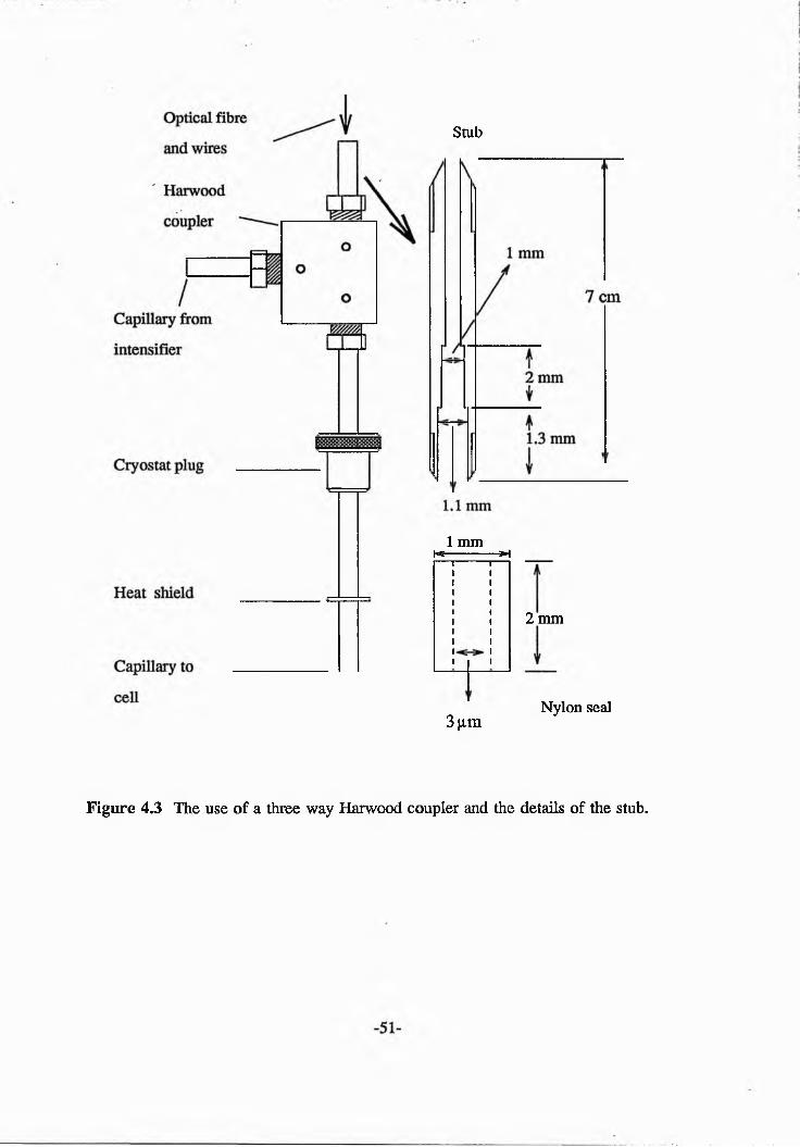
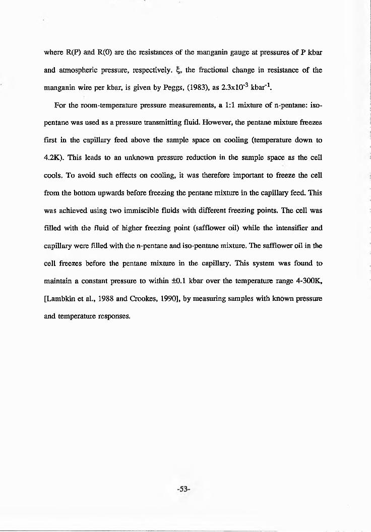
4.5.4 The High Pressure Cell
The high pressure cell designed by Lambkin et al., (1988), is shown in figure 4.4.
Capillary feed
Thrust piston
Cylinder
’O’-ring and nylon seals
Pressure transmitting fluid
Manganin gauge
Silver steel plug in Vespel sleeve
Fixed piston
Electrical leads
Backing pad
Figure 4.2 The schematic diagram of piston and cylinder high pressure apparatus.
Stub
1 mmHs--------3H
2 mm
3 jimNylon seal
Figure 4.3 The use of a three way Harwood coupler and the details of the stub.
This consists of a conventional double-walled thick cylinder made of Cu:Be with an
outer diameter of 19 mm, which allowed it to fit into a standard Oxford Instruments
continuous flow cryostat. The inner bore is 5 mm. Both pistons were sealed with O-rings
and nylon tapered rings. The bottom piston was blank; the upper piston carried the
sample mount. A capillary feed was fitted into this piston using a standard Harwood
seal. Both electrical wires and fibre were brought down the capillary through to the
sample. The capillary feed supports the cylinder in the cryostat and had two or three
radiation shields fitted at appropriate points.
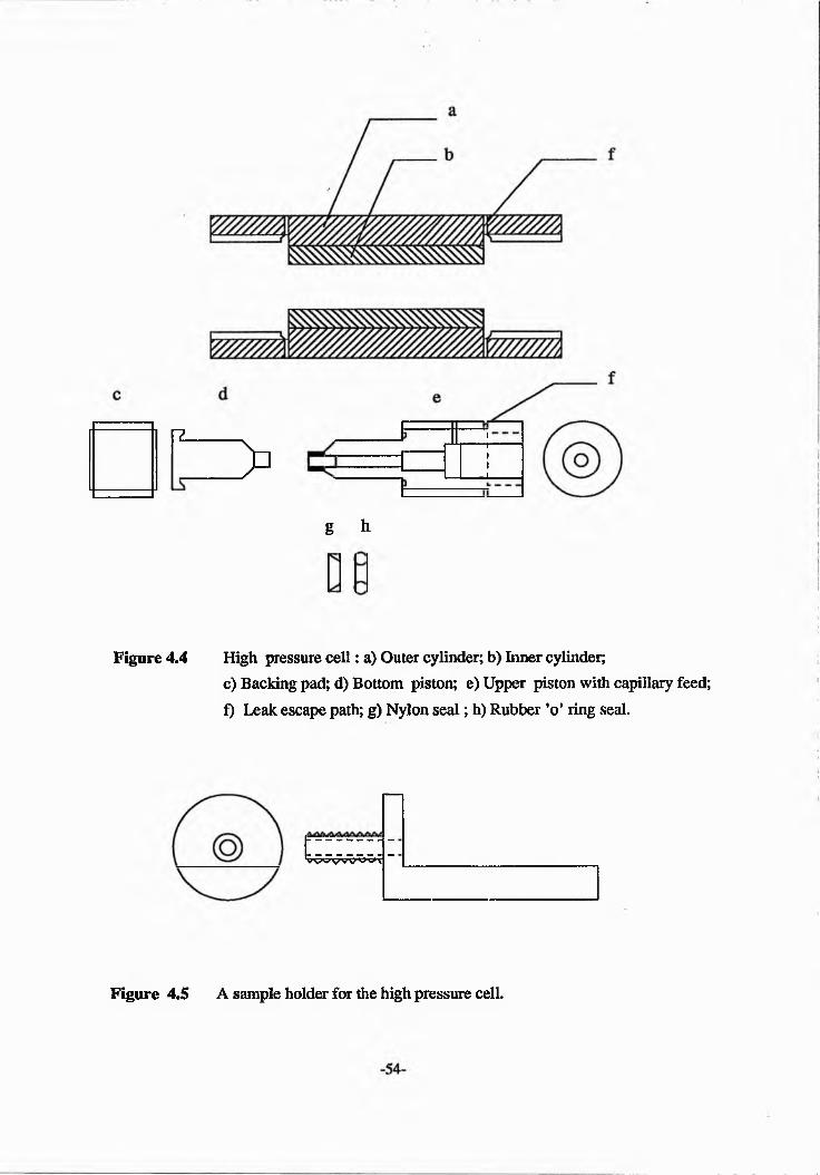
A sample holder for the high pressure cell given in figure 4.5 is easily fitted to the
upper piston of the cell shown in figure 4.4.e. Both electrical wires and fibre are brought
down to the sample holder with a capillary feed. The sample was placed on the platform
of the sample holder. Four electrical wires were then mounted to the four contacts using
the Epo Tek epoxy. It was then cured at 120°C for approximately one hour to hardened
the connections. Finally, together sample and sample holder was surrounded by PTFE
tape to prevent the moving when the pressure was applied.
The pressure generated in the standard piston and cylinder system was transmitted
via the capillary feed through to the high pressure cell, in which the sample was
mounted. The pressure in the system was measured with a manganin gauge fitted on the
bottom piston of the intensifier piston-cylinder system. The manganin gauge consisted
of a number of turns of manganin wire wound on a plastic reel, giving a resistance of
approximately 150 Q. The resistance of manganin gauge is related to the pressure (kbar)
as
P ( k b a r ) = | l n [ | { | j - ] 4 . 5 . 1
where R(P) and R(0) are the resistances of the manganin gauge at pressures of P kbar
and atmospheric pressure, respectively. the fractional change in resistance of the
manganin wire per kbar, is given by Peggs, (1983), as 2.3xl0“3 kbar-1.
For the room-temperature pressure measurements, a 1:1 mixture of n-pentane: iso-
pentane was used as a pressure transmitting fluid. However, the pentane mixture freezes
first in the capillary feed above the sample space on cooling (temperature down to
4.2K). This leads to an unknown pressure reduction in the sample space as the cell
cools. To avoid such effects on cooling, it was therefore important to freeze the cell
from the bottom upwards before freezing the pentane mixture in the capillary feed. This
was achieved using two immiscible fluids with different freezing points. The cell was
filled with the fluid of higher freezing point (safflower oil) while the intensifier and
capillary were filled with the n-pentane and iso-pentane mixture. The safflower oil in the
cell freezes before the pentane mixture in the capillary. This system was found to
maintain a constant pressure to within ±0.1 kbar over the temperature range 4-300K,
[Lambkin et al., 1988 and Crookes, 1990], by measuring samples with known pressure
and temperature responses.
~L
>
g h
Figure 4.4 High pressure ce ll: a) Outer cylinder; b) Inner cylinder;c) Backing pad; d) Bottom piston; e) Upper piston with capillary feed; f) Leak escape path; g) Nylon sea l; h) Rubber ’o’ ring seal.
'VWVWW\
Figure 4.5 A sample holder for the high pressure cell.
C h a p t e r 5
T e m p e r a t u r e D e p e n d e n c e o f H a l l M o b i l i t y a n d C a r r i e r
C o n c e n t r a t i o n i n I n ^ G a j ;[A s
5 .1 I n t r o d u c t i o n
In this chapter we analyse the Hall effect measurements with alloy composition (x)
as a function of temperature, in the range 4.2-300K. The samples studied were grown
in a VG80 MBE system at growth temperature of 530±20°C. All the samples were 3pm
thick and doped with Si to a carrier density of approximately 1016 cm"3. The theoretical
mobility has been calculated using an iterative solution o f the Boltzmann equation
(ISBE) with the values of the material parameters described in chapter 2.
The sample uniformity through the conducting region is important for the interpreta
tion of the transport data. Sample nonuniformities in the conducting region may lead to
anomalous results in the carrier density and, therefore, in the mobility. All samples have
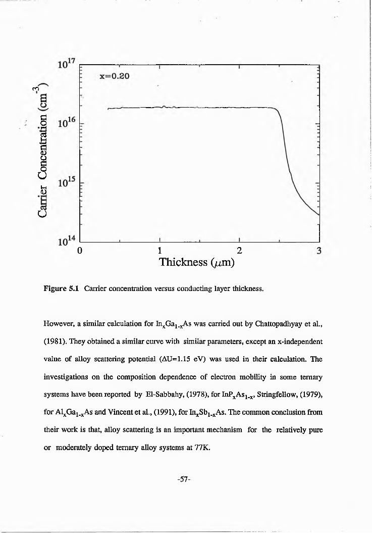
a 3pm thickness of conducting region. Figure 5.1 shows the variation of carrier concen
tration with increasing penetration through the sample measured from the top surface.
Allowing for surface and substrate depletion, we see that the carrier concentration is
constant over a large proportion of the epilayer width, then shows a sharp decrease in
the 2.5-3pm depth region. However, this small nonuniform region does not substantially
affect the carrier density which is an average over the whole active region, [Lee, 1992].
-55-
5 . 2 T h e C o m p o s i t i o n D e p e n d e n c e o f H a l l M o b i l i t y a n d
C a r r i e r C o n c e n t r a t i o n
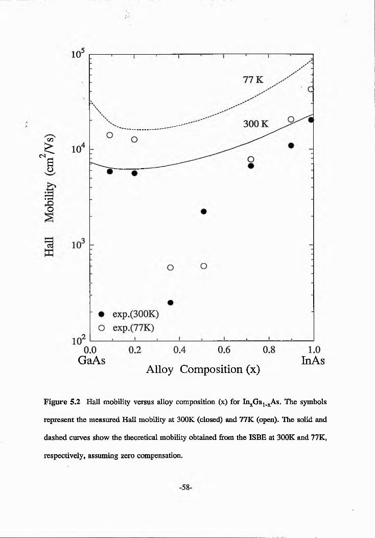
The variation of mobility with alloy composition (x) at room-temperature and 77K
is displayed in figure 5.2. The theoretical mobility has been calculated using the ISBE
including the most relevant scattering mechanisms; polar optic, acoustic deformation
potential, piezoelectric, alloy disorder and ionized impurity scattering (with Brooks-
Hening theory). Energy band non-parabolicity, electron wave function admixture,
degeneracy of distribution function and electron screening have also been incorporated.
In the calculation the electron concentration (n) was taken as lxlO16 cm"3 assuming
no compensation. Alloy scattering potential was taken to be an x-dependent parameter
as discussed in chapter 2. In the ISBE the magnetic field was used as an input parameter
having the same value as that used in the experiment.
Figure 5.2 shows the mobility versus alloy composition where, with the possible
exception of the x=0.09, the epitaxial layer is fully relaxed. The room-temperature
measured mobility agrees relatively well with theory for x<0.20 and x>0.90, while the
77K mobility reasonably agrees with theory only for x<0.20 as shown by the solid and
dashed curves, respectively, in the figure.
A most interesting feature of the calculated mobility is that it shows a minimum in
the region x=0.10 or 0.20 and an increase across the alloy composition. This increase
is related to the variation of band gap and the effective mass. The mobility minimum is
more pronounced at 77K than at room-temperature. This is due to the effect of alloy
scattering since the optical phonon and ionized impurity scattering are reduced at 77K.
cnB
la
iiuhi<d
U
0 1 2 T h i c k n e s s ( /x m )
Figure 5.1 Carrier concentration versus conducting layer thickness.
However, a similar calculation for fr^G a^A s was carried out by Chattopadhyay et al.,
(1981). They obtained a similar curve with similar parameters, except an x-independent
value of alloy scattering potential (AU=1.15 eV) was used in their calculation. The
investigations on the composition dependence of electron mobility in some ternary
systems have been reported by El-Sabbahy, (1978), for InE^A s^, Stringfellow, (1979),
for AlxGa1.xAs and Vincent et al., (1991), for I^ S b ^ A s . The common conclusion from
their work is that, alloy scattering is an important mechanism for the relatively pure
or moderately doped ternary alloy systems at 77K.
-57-
f t
CZ)
£BO
• rHo
G a A sA l l o y C o m p o s i t i o n ( x )
I n A s
Figure 5.2 Hall mobility versus alloy composition (x) for k ^ G a ^ A s. The symbols
represent the measured Hall mobility at 300K (closed) and 77K (open). The solid and
dashed curves show the theoretical mobility obtained from the ISBE at 300K and 77K,
respectively, assuming zero compensation.
Returning to the experimental mobility, at higher In compositions (x>0.20) the
mobility decreases dramatically before recovering at compositions x>0.40. Associated
with this is a dramatic decrease in the carrier density, which is given in figure 5.3, so
that for x~0.30 the epitaxial layers are semi-insulating. For the x=0.36 layer the carrier
density is thermally activated, indicating a defect level presumably associated with layer
relaxation. However, recently work on h ^ G a ^ A s, [Ekenstedt et al., 1992], has shown
a similar decrease in the mobility and carrier density. They suggest that space charge
scattering is of importance for low carrier concentration. However, they suggest no
model of why carrier concentration changes with alloy composition. For In compositions
with x>0.40 the mobility recovers partially and tends to approach the theoretically
predicted with increasing alloy composition (x). This may be due to either increased
donor compensation or to additional scattering mechanisms associated with space-charge
scattering or scattering from a dislocation network as alloy composition (x) decreases
from the end binary InAs toward x~0.36.
Figure 5.3 shows the measured carrier concentration versus alloy composition at the
room-temperature. The carrier density shows a dramatic decrease at x -0.36 as did the
mobility. There are two possible mechanisms responsible for this decrease. The first
possibility is that the autocompensation mechanism may occur around x-0.40 and decays
with increasing In content. Si doped GaAs and InAs grown by MBE have been reported
to be shown the autocompensation mechanism, [Chai et al., 1981, and Kubiak et al.,
1984]. Si atoms can occupy Ga or In sites to form donors (in the case of GaAs and/
InAs, respectively) but may also be incorporated As side to form acceptors. The
negatively charged Si atoms (acceptors) and positively charged Si atoms (donors) will
then be autocompensated to form neutral pairs.
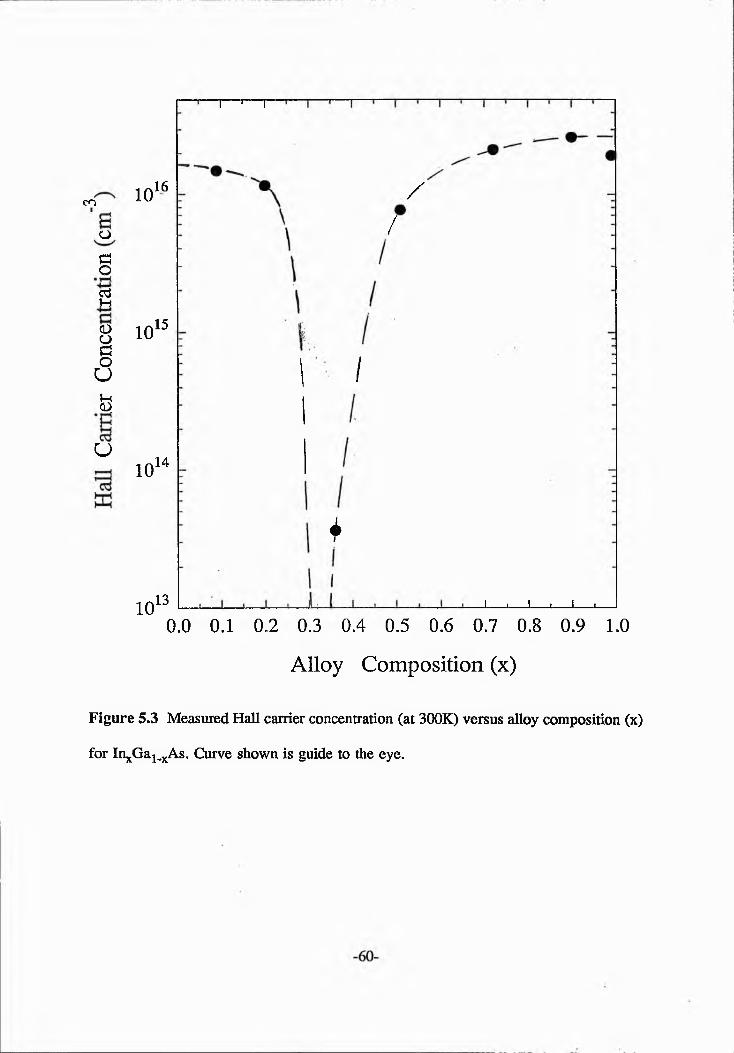
cn
u
1016
o
£5o
s8 ioao
UVh04
15
1014
10 13
i 1 r
/
/
r /
i
4
J I i I ! L.0.0 0.1 0.2 0.3 0.4 0.5 0.6 0.7 0.8 0.9 1.0
A l l o y C o m p o s i t i o n ( x )
Figure 5.3 Measured Hall carrier concentration (at 300K) versus alloy composition (x)
for fr^G a^A s. Curve shown is guide to the eye.
In the case of Ii^G a^A s, Si atoms may occupy both group ID and As sites to form
donors and acceptors as in the case of GaAs and InAs. The occupancy factor of group
HI sites ( positively charged Si atoms) may be increased by decreasing Ga content (or
increasing In content) while the occupancy factor of As sites (negatively charged Si
atoms) stays constant due to the constant As flux in the growth processes. The very low
carrier density at the 0.20<x^0.51 layers are indicating these two factors are probably
balanced (i.e. autocompensation occurs). For the x>0.51 layers, the autocompensation
decays so that the carrier density increases. However, it should be noted that the reported
autocompensation mechanism in GaAs and InAs occurs above a Si-doping concentration
of 1018cm"3, [Chai et al., 1981, and Kubiak et al., 1984].
A second possibility is that these effects are due to defect levels generated in
association with layer relaxation. An increase in the layer relaxation with increased In
content may result an increased number of defect levels. In addition to this, the absolute
energy of such levels may change with In concentration. These effects will be
investigated in more detail by analyzing the temperature and pressure dependence of
mobility and carrier concentration in the next chapter. We will see the electron trap out
with temperature and pressure significantly increases from the two end binaries through
x~0.4. If the sharp decrease is due to the autocompensation we do not expect any
significant change in the electron trap out with temperature and pressure across the alloy
composition.
In conclusion, as a consequence either the effects of autocompensation or the defect
levels associated with the layer relaxation or the effects of both these mechanisms, the
carrier density as well as the mobility decreases at 0.20<x<0.60 in InxGa1_xAs.
However, to our knowledge, no experimental reports shows such a dramatic decrease
either in the carrier density or the mobility with alloy composition in any other lattice-
matched or strained ternary systems.
5 . 3 T e m p e r a t u r e D e p e n d e n c e o f t h e M o b i l i t y a n d
C a r r i e r C o n c e n t r a t i o n
In this section we analyse our experimental results for the temperature dependence
of the electron Hall mobility using the ISBE as discussed in a previous section. The
temperature dependence of Hall mobility for six samples of I ^ G a ^ A s (In percentage
indicated in the figure) is given in figure 5M The symbols represent the experimental
mobility. The solid curves represent the best fit to the experimental mobility calculated
by the ISBE allowing carrier concentration to vary with temperature. In the calculations
the compensation ratio (k=NA/ND) given in table 5.1 is given for each sample by using
NA(acceptor concentration) as an adjustable parameter by fitting the ionized impurity
scattering mechanism at 300K.
The experimental mobility of all samples, with the exception of the x=0.51 sample,
exhibits the general characteristic of extrinsic III-V semiconductors. The high tempera
ture mobility is limited by the polar optical phonon scattering which is shown by the
increase in the mobility as the temperature decreases. This is due to the decrease in the
density of the polar phonon. However, in this temperature range ionized impurity
scattering has a significant influence on the overall mobility. The mobility has a
maximum near 90K, being limited by ionized impurity scattering at the intermediate
temperatures. For III-V semiconductors it is expected that the acoustic phonon scattering
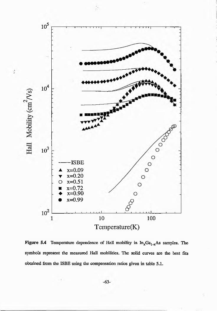
10 '
C/3
£o
rOO
10
10 :
10 '
*i----1—i i i i ry TT
■ umnmmnrnf*'
ISBEA x=0.09 t x=0.20 O x=0.51■ x=0.72♦ x=0.90• x=0.99
____i___ i__ i i i_i_i_i_
&&J___ I__ I_I_I_I_I_L. j ______ i
10 100
T e m p e r a t u r e ( K )
Figure 5.4 Temperature dependence of Hall mobility in In^G a^A s samples. The
symbols represent the measured Hall mobilities. The solid curves are the best fits
obtained from the ISBE using the compensation ratios given in table 5.1.
(deformation potential at high temperatures and piezoelectric at low temperatures) have
a significant effect on the overall mobility. However, when we cancelled out these
scattering mechanisms in the ISBE, we did not find any significant change in the
temperature dependence of mobility for the x>0.2 samples.
The other interesting feature of the experimental mobility is that the small and
virtually constant mobility at low temperatures (4.2-3OK). In this temperature range for
the x<0.2 samples the mobility is lower than the room temperature mobility, and slightly
temperature dependent while the mobility of the other samples tends to be constant. This
low temperature behaviour is connected with the temperature dependence of the carrier
concentration, and indicates the impurity conduction is occurring at low temperatures.
This process will be described in more detail in the rest of this section.
The solid curves in the figure were calculated using the compensation ratios given
in the table 5.1. Good agreement is obtained for temperatures between 300 and 70K for
all samples, except x=0.51. We found the best fit using the alloy scattering potential
slightly higher than the values of 1.06[x(l-x)]1̂2 for the x>0.51 samples. Their values
are also given in table 5.1 for comparison. This may be because the alloy scattering
potential slightly increases with increased alloy composition (x), or that the space-charge
scattering effect increases with increasing compensation ratio as suggested by
Stringfellow, (1979), and Stringfellow and Kiinzel, (1980), for A ^G a^A s.
The theoretical mobility reaches a maximum near 90K as does the experimental
mobility, and tends to decrease more slowly than experiment. At low temperatures the
ISBE predicts nearly constant, but higher than measured mobility. This is connected to
the measured carrier concentration. The carrier concentration of each sample, except
x=0.51, becomes to degenerate at the temperature which close to carrier concentration
minimum. In this case the mobility is calculated by varying the occupancy of states at
the Fermi level. For such a degenerate electron distribution the mobility is independent
of temperature.
If we now return to the temperature dependence of carrier concentration given in
figure 5.5, the measured carrier concentration exhibits a similar behaviour with tempera
ture. The temperature dependence of carrier concentration exhibits a characteristic
minimum associated with carrier transfer in two-band conduction.
This behaviour of the carrier concentration makes it is impossible to determine the
impurity contents ND, NA and Ed from the analysis of measured carrier concentration
using the usual expression given in equation 2.5.3. However, in principle the carrier
concentration in the conduction band nc(T) and in the impurity band n^T) can be
determined from the measured carrier concentration using the two-band model described
by Emel’yanenko et al., (1965). We now give a brief discussion of their model. They
gave the following expression for the two-band conduction, assuming that the Hall effect
for the electrons in the impurity band is given by the same formula as that for
elections in the conduction band (R ^/en j, r« l)
N0_ (x+b2) (x + l) 5.3.1n (x+b )2
where b=|ic/pi , x=nj/nc , N ^np+ n^onstan t, and n is the measured carrier concentra
tion.
The measured carrier concentration exhibits a minimum when ncjxc=ni(Lti. In their model
b is assumed to be independent of temperature and it can be worked out from equation
5.3.1 as
-65-
No - / b + 1 \ 2 r W 4b
5 . 3 . 2
In the past Hall factor r for the impurity band was assumed that r~ l, but there is no
available clear evidence. The assumption of temperature independent mobility ratio leads
to the conduction band and impurity band mobility have the similar temperature
dependence. This means the carriers in the impurity band are scattered by the same
centres as in the conduction band. This is also not yet clear.
The assumption of N0=nc+ni=const. is likely be true but, it is difficult to estimate the
value of N0 from the measured carrier concentration. Their observed temperature
dependence of the carder density shows that it has almost equal values at the highest
and lowest temperatures. This is only approximately true for our temperature dependence
of carrier concentration as can be seen in figure 5.5.
The calculated nc(T) using this model simultaneously decreases without having a
thermal saturation with decreasing temperature. This causes the difficulties in the
determining the impurity contents.
For these reasons, we avoided calculating nc(T) and n /T ) and performing detailed
analysis using the two-band model. However, the calculation of impurity contents from
the analysis of the temperature dependence of carrier concentration in the conduction
band is complicated by the impurity conduction, so that in this case we prefer to
determine ND and NA from the mobility analysis via ionized impurity scattering. They
will be used for impurity band calculations in later chapters. Therefore, we will give a
qualitative analysis instead of quantitative one for the temperature dependence of the
carrier concentration.
-66-
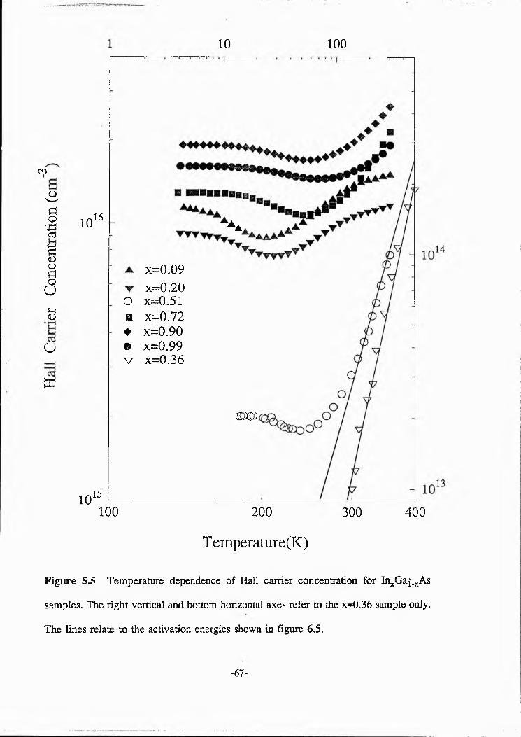
10 100
cn
3do
■s4—>d<Dodo
UVh<D
u
ffi
10 16
10 15
AA
x=0x=0
O x=0 m x=0 ♦ x=0, m x= 0 . v x=0
.09
.2 0
.51
.72
.9099.36
m ®
100 2 0 0 300
T e m p e r a t u r e ( K )
4 0 0
Figure 5.5 Temperature dependence of Hall carrier concentration for In^Gaj^As
samples. The right vertical and bottom horizontal axes refer to the x=0.36 sample only.
The lines relate to the activation energies shown in figure 6.5.
-67-
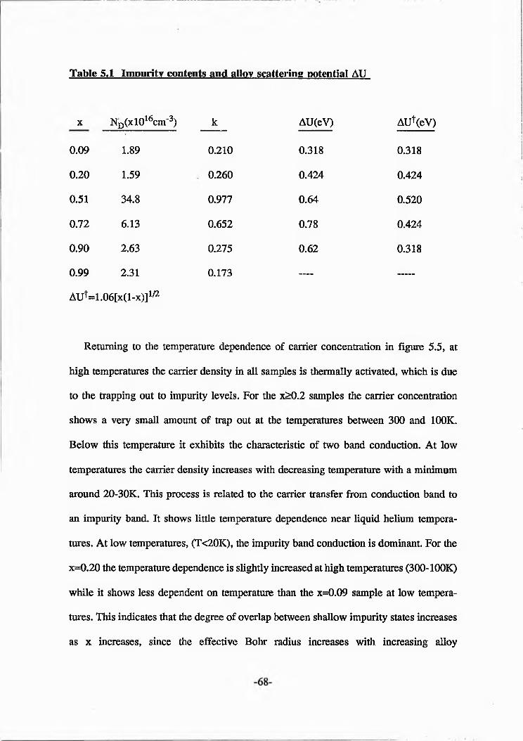
Table 5.1 Impurity contents and alloy scattering potential AU
x ND(xl016cm"3) k AU(eV) AU+CeV)
0.09 1.89 0.210 0.318 0.318
0.20 1.59 0.260 0.424 0.424
0.51 34.8 0.977 0.64 0.520
0.72 6.13 0.652 0.78 0.424
0.90 2.63 0.275 0.62 0.318
0.99 2.31 0.173 —
AU1==1.06[x(l-x)]1/2
Returning to the temperature dependence of carrier concentration in figure 5.5, at
high temperatures the carrier density in all samples is thermally activated, which is due
to the trapping out to impurity levels. For the x>0.2 samples the carrier concentration
shows a very small amount of trap out at the temperatures between 300 and 100K.
Below this temperature it exhibits the characteristic of two band conduction. At low
temperatures the carrier density increases with decreasing temperature with a minimum
around 20-30K. This process is related to the carrier transfer from conduction band to
an impurity band. It shows little temperature dependence near liquid helium tempera
tures. At low temperatures, (T<20K), the impurity band conduction is dominant. For the
x=0.20 the temperature dependence is slightly increased at high temperatures (300-100K)
while it shows less dependent on temperature than the x=0.09 sample at low tempera
tures. This indicates that the degree of overlap between shallow impurity states increases
as x increases, since the effective Bohr radius increases with increasing alloy
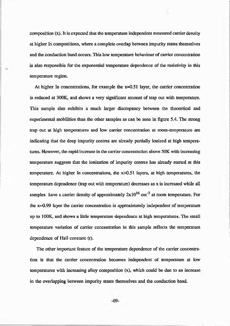
composition (x). It is expected that the temperature independent measured carrier density
at higher In compositions, where a complete overlap between impurity states themselves
and the conduction band occurs. This low temperature behaviour of carrier concentration
is also responsible for the exponential temperature dependence of the resistivity in this
temperature region.
At higher In concentrations, for example the x=0.51 layer, the carrier concentration
is reduced at 300K, and shows a very significant amount of trap out with temperature.
This sample also exhibits a much larger discrepancy between the theoretical and
experimental mobilities than the other samples as can be seen in figure 5.4. The strong
trap out at high temperatures and low carrier concentration at room-temperature are
indicating that the deep impurity centres are already partially ionized at high tempera
tures. However, the rapid increase in the carrier concentration above 50K with increasing
temperature suggests that the ionization of impurity centres has already started at this
temperature. At higher In concentrations, the x>0.51 layers, at high temperatures, the
temperature dependence (trap out with temperature) decreases as x is increased while all
samples have a carrier density of approximately 2x l016 cm-3 at room temperature. For
the x=0.99 layer the carrier concentration is approximately independent of temperature
up to 100K, and shows a little temperature dependence at high temperatures. The small
temperature variation of carrier concentration in this sample reflects the temperature
dependence of Hall constant (r).
The other important feature of the temperature dependence of the carrier concentra
tion is that the carrier concentration becomes independent of temperature at low
temperatures with increasing alloy composition (x), which could be due to an increase
in the overlapping between impurity states themselves and the conduction band.
T able 5.2 The measured n u R / B n ^ W a ^ n a w A k „.- and the tempe.ah.re nf
the carrier concentration minimum flrmin) for In G,^ xAs.
x n4.2K^nmin n 300K/nmin M-300k /M-4.2K T m in(K )
0.09 1.28 1.68 2.53 20
0.20 1.27 1.53 1.91 28
0.51 — 4.30 — 48
0.72 1.20 1.99 1.76 50
0.90 1.14 1.56 0.89 60
0.99 1.12 1.33 0.80 80
If we now compare the temperature dependence of mobility from figure 5.4 with the
temperature dependence of carrier concentration from figure 5.5, it can be seen that the
mobility maximum and the minimum in the carrier concentration do not occur at the
same temperature. The mobility decreases just above and below the temperature where
the carrier concentration minimum occurs because of the carrier transferring from the
conduction band to the impurity band. At low temperatures the mobility and carrier
concentration are slightly temperature dependent (for x<0.20) or independent of tempera
ture (for x>0.51), so that the impurity conduction is dominant and the conduction band
mobility is negligible.
It is convenient to consider the temperature dependence of mobility in three
temperature regions; the high temperature region where only the conduction band
mobility is dominant so that the ISBE is in good agreement in this temperature region.
The intermediate temperature or transition (carrier transfer) region, where both the
conduction band and impurity band mobilities are significantly affecting the overall
mobility, and the low temperature region, where only the impurity conduction is
dominant.
It should be noted that the minimum in the carrier concentration is shifted to higher
temperatures, and the depth of minimum is getting smaller as alloy composition (x) is
increased which can be seen more clearly in table 5.2. In addition to this, at low
temperatures, the mobility and carrier concentration become independent of temperature
with increasing alloy composition (x). These indicate that the impurity band conduction h*-
effects may'‘extended to higher temperatures, and in the impurity band metallic
conduction takes place instead of the activated hopping conduction with increasing x.
We shall deal with these two phenomena further in chapter 7.
5 . 4 T e m p e r a t u r e D e p e n d e n c e o f M o b i l i t y a n d C a r r i e r
C o n c e n t r a t i o n i n t h e x = 0 . 5 1 a n d 0 . 6 0 S a m p l e s
In section 5.2, a sharp decrease in the mobility and carrier concentration has been
observed for a limited alloy composition range, x=0.30-0.51. However, in the last section
we have shown that the ISBE is in good agreement with the experimental temperature
dependence of mobility for a wide temperature range (300-70K) for limited alloy
composition range x<0.20 and x>0.51. In this section we now discuss the temperature
dependence of electron mobility and carrier concentration for the x=0.51 and two
Ino goGao.40As samples, which were grown at different substrate temperatures, since they
exhibit a similar behaviour with temperature.
Figure 5.6 shows the temperature dependence of the Hall mobility for x=0.51 and
two In0 60Ga0 4(j As samples. The lines in the figure represent the theoretical mobilities
calculated using the ISBE with compensation ratios indicated in the figure. The
experimental mobility in all samples decreases more rapidly than the theoretical mobility
with decreasing temperature. The changes in the growth temperature Tgr do not affect
the temperature dependence of mobility strongly, as can be seen in the figure. The room
temperature mobility and the measured temperature dependence of mobility (jiaTm) are
slightly decreased by reducing the growth temperature Tgr. This is connected with the
temperature dependence of carrier concentration given in figure 5.7. This is seen more
clearly from the values m, M-300K/M77K and n3ooK/n77K in tab*e 5.3.
From figure 5.6 it can be seen that the ISBE produces a clear discrepancy with the
measured Hall mobilities across a wide range of temperature. The dependence on
temperature (m) is changing between 1.2 and 1.7 as can be seen in the table 5.3. This
is in contrast with the results of Stringfellow, (1979), Strinfellow and Kiinzel, (1980) for
A ^ G a^ A s, and Ekenstedt et al., (1992) for InxGa1-xAs. The former authors have shown
that the space charge scattering (fxaT1,2) effect is increased by increasing the compensa
tion ratio, and it causes a significant reduction in the electron mobility. We found no
clear contribution from space charge scattering in either the temperature or the pressure
dependence of mobility for the x<0.20 and x>0.51 samples.
Recently Ekenstedt et al., (1992), indicated that good agreement between theory and
experiment may be obtained by accounting for the dislocation scattering in the
calculation. If we speculate on the temperature dependence of an additional scattering
mechanism we find using a Matthissens rule approach, that the additional mechanism
should have a T t'm where 2.34<m<2.84 (or -2.6). None of the published formulations
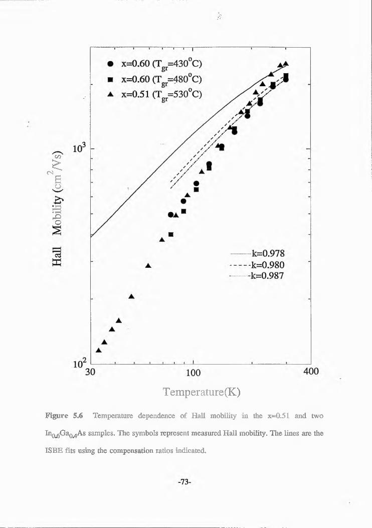
04
CZ)
£Bo
r 342O
T e m p e r a t u r e ( K )
Figure 5.6 Temperature dependence of Hall mobility in the x=0.51 and two
InQ 6Ga04As samples. The symbols represent measured Hall mobility. The lines are the
ISBE fits using the compensation ratios indicated.
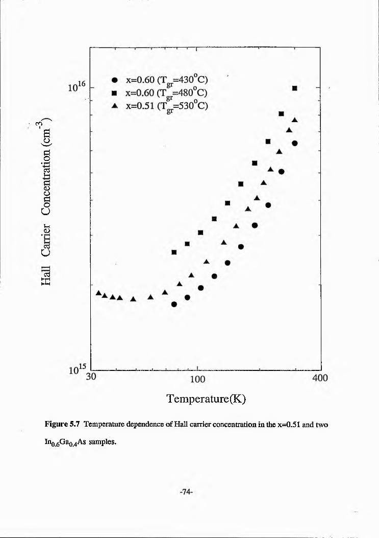
coa
f j ,
do• T—ja<DOdo
UIhCD
u
03EC
T e m p e r a t u r e ( K )
Figure 5.7 Temperature dependence of Hall carrier concentration in the x=0.51 and two
Ino 6Gao 4As samples.
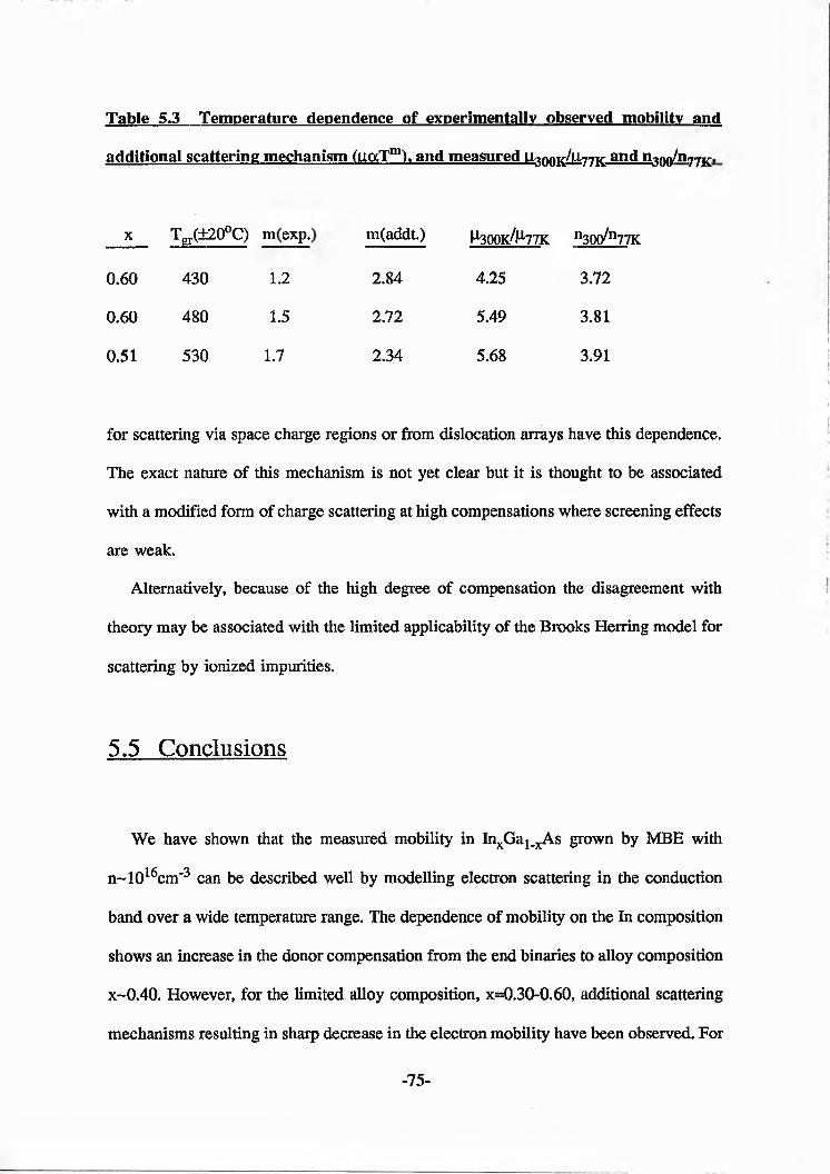
Table 5.3 Temperature dependence of experimentally observed mobility and
additional scattering mechanism (iiaTm). and measured u^qqk^ tk and n300/n77K.
X Ter(±20°C) B 1 m(addt.) M'300k/M'77K n30(/n77K
0.60 430 1 .2 2.84 4.25 3.72
0.60 480 1.5 2.72 5.49 3.81
0.51 530 1.7 2.34 5.68 3.91
for scattering via space charge regions or from dislocation arrays have this dependence.
The exact nature of this mechanism is not yet clear but it is thought to be associated
with a modified form of charge scattering at high compensations where screening effects
are weak.
Alternatively, because of the high degree of compensation the disagreement with
theory may be associated with the limited applicability of the Brooks Herring model for
scattering by ionized impurities.
5 . 5 C o n c l u s i o n s
We have shown that the measured mobility in InxGaj.xAs grown by MBE with
n~1016crri3 can be described well by modelling electron scattering in the conduction
band over a wide temperature range. The dependence of mobility on the In composition
shows an increase in the donor compensation from the end binaries to alloy composition
x~0.40. However, for the limited alloy composition, x=0.30-0.60, additional scattering
mechanisms resulting in sharp decrease in the electron mobility have been observed. For
-75-
the x=0.51 and 0.60 layers an additional scattering mechanism having an effective
temperature dependence of ~T2*6 has been found.
The standard model ISBE fails to predict the temperature dependence of mobility at
low temperatures where impurity conduction occurs. The evidence that impurity
conduction is occurring at low temperatures in both samples is the minimum in the
carrier concentration versus temperature and the low and virtually constant mobility. The
low temperature behaviour of the carrier concentration indicates that metallic conduction
takes place instead of the thermally activated hopping conduction in the impurity band
with increasing alloy composition (x).
The measured carrier concentration shows a dramatic decrease in the limited alloy
composition range 0.20<x<0.60, as does the mobility. The amount of trap out with
temperature also increases through the middle of alloy composition range. This
behaviour of the carrier concentration, the sharp decrease and significant trap out with
temperature, may be due to a defect level associated with the layer relaxation. This
suggests that samples which exhibits significant trap out with temperature will also show
a significant trap out with pressure. These effects are investigated in the next chapter.
C h a p t e r 6
T e m p e r a t u r e a n d P r e s s u r e D e p e n d e n c e o f M o b i l i t y a n d
C a r r i e r C o n c e n t r a t i o n
6 .1 I n t r o d u c t i o n
In this chapter we analyse our experimental results both as a function of temperature
(4.2-300K) and pressure (0-8 kbar) for In]CGa1.xAs> using the ISBE as used in the
previous chapter. This chapter naturally splits in two sections. In the first section we
discuss the pressure dependence of Hall mobility and carrier concentration at room-
temperature. The second section discusses the temperature dependence of mobility and
carrier concentration as a function of pressure in the range 0-8 kbar. However, we
discuss the temperature and pressure dependence of mobility and carrier concentration
for the x=0.51 and 0.60 samples in a separate section as in the previous chapter.
6 . 2 R o o m T e m p e r a t u r e P r e s s u r e D e p e n d e n c e o f C a r r i e r
C o n c e n t r a t i o n a n d M o b i l i t y
The pressure dependence of Hall carrier concentration and mobility normalised to
atmospheric pressure are given in figures 6.1 and 6.2, respectively. Two different results
-77-
have been observed from the pressure dependence of carrier concentration, as can be
seen in figure 6.1. For the In compositions x<0.20 and x=0.99 the carrier concentration
shows a very small trap out with pressure, as was expected from the temperature
dependence of carrier concentration at high temperatures discussed in the previous
chapter. We, therefore, expect that such a small trap out with pressure does not
significantly effect the pressure dependence of mobility, particularly for the x<0.20
samples. For the limited alloy composition, x=0.51-0.90, the carrier concentration shows
a strong trap out with pressure. In addition to this, in this alloy composition range, the
trap out with pressure decreases with increasing alloy composition (x).
Trap out with pressure across the alloy composition supports the conclusion
obtained for the temperature dependence of carrier concentration in the previous chapter,
or vice versa. However, we examine in more detail the pressure and temperature
dependence of mobility, and its relationship with the trap out with temperature and
pressure in the rest of this chapter.
Figure 6.2 shows the normalised pressure dependence of Hall mobility versus
pressure. The application of pressure increases the band gap and hence the electron
effective mass. The deep levels do not move with the band edge, deep levels become
deeper with pressure. However, the pressure dependence of effective mass increases
from GaAs to InAs as discussed in chapter 2. This alone should lead to an increase in
the pressure dependence of electron mobility across to alloy composition. Secondly we
discuss how the deep levels effect the pressure dependence of mobility.
The pressure dependence of mobility in both samples shows an approximately linear
decrease with increasing pressure as can be seen in figure 6.2. It is difficult to
distinguish the pressure dependence of mobility on the alloy composition using the
No
rmal
ized
H
all
Car
rier
C
on
ce
ntr
ati
on
1.0
0.9
0 .8
0.7
0 .6
0.5
0.4
,A A
• x=0.99
a x=0.09
■ x=0.20
♦ x=0.72
▼ x=0.51
0 2 4 6 8 10
P r e s s u r e ( k b a r )
Figure 6.1 The 300K normalised pressure dependence of Hall carrier concentration for
Ir^G a^ A s samples.
P r e s s u r e ( k b a r )
Figure 6.2 The 300K normalised pressure dependence of Hall mobility for I ^ G a ^ A s
samples.
-80-
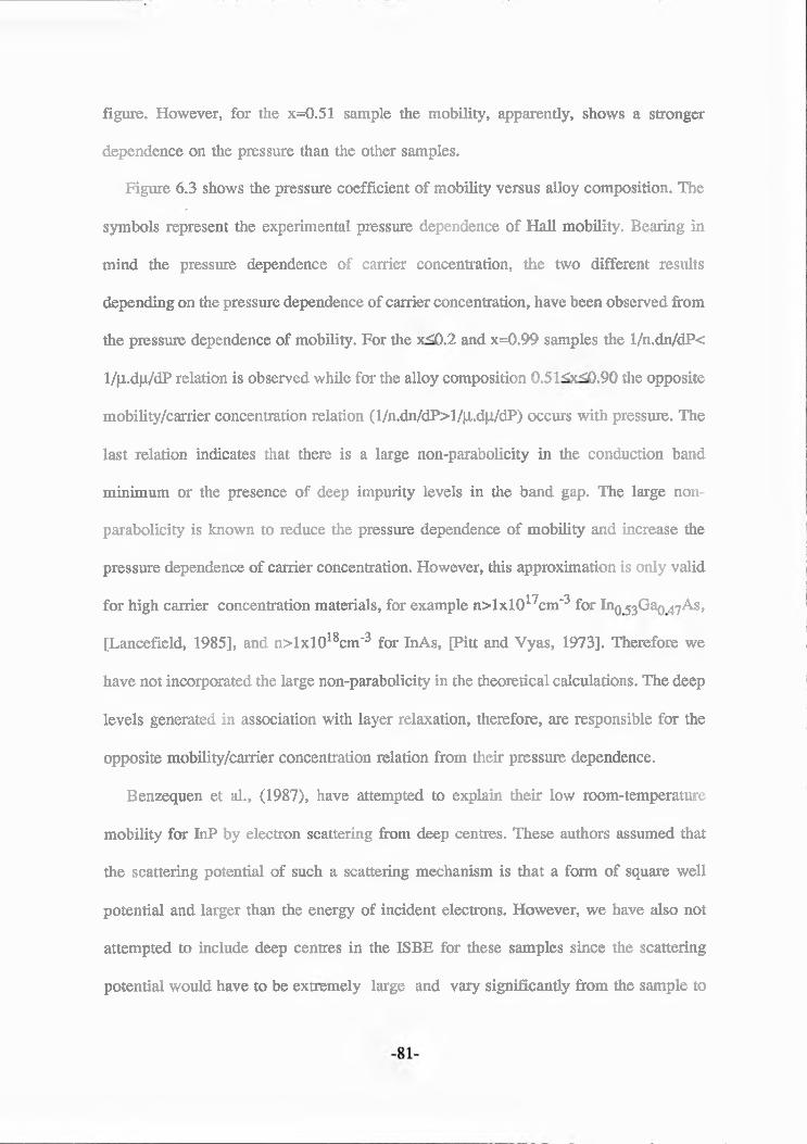
figure. However, for the x=0.51 sample the mobility, apparently, shows a stronger
dependence on the pressure than the other samples.
Figure 6.3 shows the pressure coefficient of mobility versus alloy composition. The
symbols represent the experimental pressure dependence of Hall mobility. Bearing in
mind the pressure dependence of carrier concentration, the two different results
depending on the pressure dependence of carrier concentration, have been observed from
the pressure dependence of mobility. For the x<0.2 and x=0.99 samples the l/n.dn/dP<
1/ji.djn/dP relation is observed while for the alloy composition 0.51<x<0.90 the opposite
mobility/carrier concentration relation ( l/n.dn/dP>l/ji.dp/dP) occurs with pressure. The
last relation indicates that there is a large non-parabolicity in the conduction band
minimum or the presence of deep impurity levels in the band gap. The large non-
parabolicity is known to reduce the pressure dependence of mobility and increase the
pressure dependence of carrier concentration. However, this approximation is only valid
for high carrier concentration materials, for example n > lx l0 17cm“3 for InQ53GaQ47As,
[Lancefield, 1985], and n > lx l0 18cm"3 for InAs, [Pitt and Vyas, 1973]. Therefore we
have not incorporated the large non-parabolicity in the theoretical calculations. The deep
levels generated in association with layer relaxation, therefore, are responsible for the
opposite mobility/carrier concentration relation from their pressure dependence.
Benzequen et al., (1987), have attempted to explain their low room-temperature
mobility for InP by electron scattering from deep centres. These authors assumed that
the scattering potential of such a scattering mechanism is that a form of square well
potential and larger than the energy of incident electrons. However, we have also not
attempted to include deep centres in the ISBE for these samples since the scattering
potential would have to be extremely large and vary significantly from the sample to
A l l o y C o m p o s i t i o n ( x )
Figure 6.3 Pressure dependence of Hall mobility versus alloy composition (x). The
solid symbols are the experimental points. The solid curve is the pressure dependence
of mobility calculated by the ISBE assuming zero compensation.
sample for the estimated number of the deep centres, [Benzaquen et al., 1987 and
1988]. The increased scattering potential for a deep level compared to a shallow level
may come from its central cell potential of the deep level. Such a scattering potential
could not be included in the ISBE as it could not be considered a small perturbation of
electron’s energy and therefore the Bom approximation would not be valid to calculate
its cross section. To include such a mechanism in the calculation of the theoretical
mobility would require a phase shift calculation, [Benzaquen et al., 1987].
We now discuss the experimentally observed pressure dependence of mobility and
theoretically predicted by the ISBE, which now incorporates the pressure dependence of
material parameters as discussed in chapter 2. In the calculation, carrier concentration
(n) was taken as ix l0 16cm'3 assuming no change in carrier concentration with pressure
and no compensation. The ISBE predicts an approximately linear increase with a little
bowing upward in the pressure dependence of mobility across the alloy composition (x)
as can be seen in figure 6.3. This is due to the variation in the pressure dependence of
electron effective mass with the alloy composition (x).
For the In composition x<0.20 the measured pressure dependence of mobility agrees
reasonably with theory, but is slightly lower than the values predicted theoretically by
the ISBE. At higher In compositions the ISBE produces a clear discrepancy with the
experimental pressure dependence of the mobility. This, except for x=0.51 sample, is
related to the measured carrier concentration via the dominant scattering mechanism.
Indeed, in the next section when we used the measured carrier concentration in the
ISBE we find a very good agreement between theory and experiment for the x<0.20
samples but we see a very poor agreement for the In compositions x>0.51. However, the
large discrepancy between theory and experiment can not be explained with such a
simple argument. Therefore this discrepancy is due to the electron scattering from the
deep centres.
For the x<0.20 samples the small trap out with pressure and temperature (at high
temperatures) is indicating that there is a very small number of deep levels which do
not effect the mobility strongly. Therefore, the ISBE gives relatively good agreement
with the experimental pressure dependence of mobility for these samples. At In
composition x=0.51 the pressure dependence of mobility is significantly increased, and
it shows quite different behaviour to the other samples. There are a number of effects
responsible for the high pressure and temperature dependence of this sample. They will
be discussed in the rest of this chapter.
For In compositions x>0.51 the trap out with pressure decreases with increasing alloy
composition (x), as does the trap out with temperature. Eventually the pressure
dependence of mobility, except the x=0.99 samples, follows the same trend with
increasing alloy composition. If the decrease in the carriers with temperature is due to
the deep centres, then it suggests that the deep centres are partially ionized at room-
temperature. Therefore, we could expect that a number of ionized deep centres falls as
pressure is increased. In addition to an increased in the room-temperature carrier
concentration for the alloy compositions x>0.51, the observed decrease in the trap out
with temperature and pressure as alloy composition (x) increases, also suggests that the
effect of deep levels on the electron transport decreases with increasing alloy
composition (x). If the deep centres are scattering strongly at room-temperature as
electrons trap out the scattering from them would then be reduced, since neutral
impurities do not scatter so strongly. The degree of reduction in the scattering rate is
related to the trap out of carriers. If the reduction in the scattering rate due to neutral
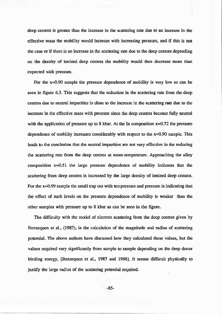
deep centres is greater than the increase in the scattering rate due to an increase in the
effective mass the mobility would increase with increasing pressure, and if this is not
the case or if there is an increase in the scattering rate due to the deep centres depending
on the density of ionized deep centres the mobility would then decrease more than
expected with pressure.
For the x=0.90 sample the pressure dependence of mobility is very low as can be
seen in figure 6.3. This suggests that the reduction in the scattering rate from the deep
centres due to neutral impurities is close to the increase in the scattering rate due to the
increase in the effective mass with pressure since the deep centres become fully neutral
with the application of pressure up to 8 kbar. At the In composition x=0.72 the pressure
dependence of mobility increases considerably with respect to the x=0.90 sample. This
leads to the conclusion that the neutral impurities are not very effective in the reducing
the scattering rate from the deep centres at room-temperature. Approaching the alloy
composition x=0.51 the large pressure dependence of mobility indicates that the
scattering from deep centres is increased by the large density of ionized deep centres.
For the x=0.99 sample the small trap out with temperature and pressure is indicating that
the effect of such levels on the pressure dependence of mobility is weaker than the
other samples with pressure up to 8 kbar as can be seen in the figure.
The difficulty with the model of electron scattering from the deep centres given by
Benzequen et al., (1987), is the calculation of the magnitude and radius of scattering
potential. The above authors have discussed how they calculated these values, but the
values required vary significantly from sample to sample depending on the deep donor
binding energy, [Benzequen et al., 1987 and 1988]. It seems difficult physically to
justify the large radius of the scattering potential required.
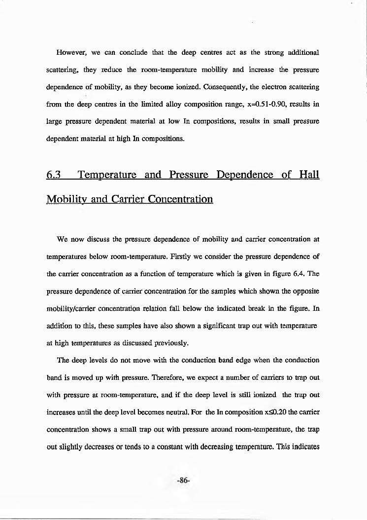
However, we can conclude that the deep centres act as the strong additional
scattering, they reduce the room-temperature mobility and increase the pressure
dependence of mobility, as they become ionized. Consequently, the electron scattering
from the deep centres in the limited alloy composition range, x=0.51-0.90, results in
large pressure dependent material at low In compositions, results in small pressure
dependent material at high In compositions.
6 . 3 T e m p e r a t u r e a n d P r e s s u r e D e p e n d e n c e o f H a l l
M o b i l i t y a n d C a r r i e r C o n c e n t r a t i o n
We now discuss the pressure dependence of mobility and carrier concentration at
temperatures below room-temperature. Firstly we consider the pressure dependence of
the carrier concentration as a function of temperature which is given in figure 6.4. The
pressure dependence of carrier concentration for the samples which shown the opposite
mobility/carrier concentration relation fall below the indicated break in the figure. In
addition to this, these samples have also shown a significant trap out with temperature
at high temperatures as discussed previously.
The deep levels do not move with the conduction band edge when the conduction
band is moved up with pressure. Therefore, we expect a number of carriers to trap out
with pressure at room-temperature, and if the deep level is still ionized the trap out
increases until the deep level becomes neutral. For the In composition x<0.20 the carrier
concentration shows a small trap out with pressure around room-temperature, the trap
out slightly decreases or tends to a constant with decreasing temperature. This indicates
1/n
. d
n/d
P ”i r~ i i i i j tt 'ml a.
0 .0 0 0 'A
x=0.09 . r Y T rT T Vv
-0.005 - A T x -°-2 0
tt% / /- ° - 0 1 0 h # * x = 0 . 9 9
-0 .0 2 / yA
-0.03 r
x=0.90-0.04
-0.05
-0.06 ^ „ ■ ■ ■ ■" x=0.72
-0.07
-0.08 O :
-0.09 1 x=0.51 or ^ C P
-0 .1 0 r c P n D c PO
-0 .1 11 10 100
T e m p e r a t u r e ( K )
Figure 6.4 Pressure dependence of Hall carrier concentration versus temperature for six
InxG a1_xAs samples.
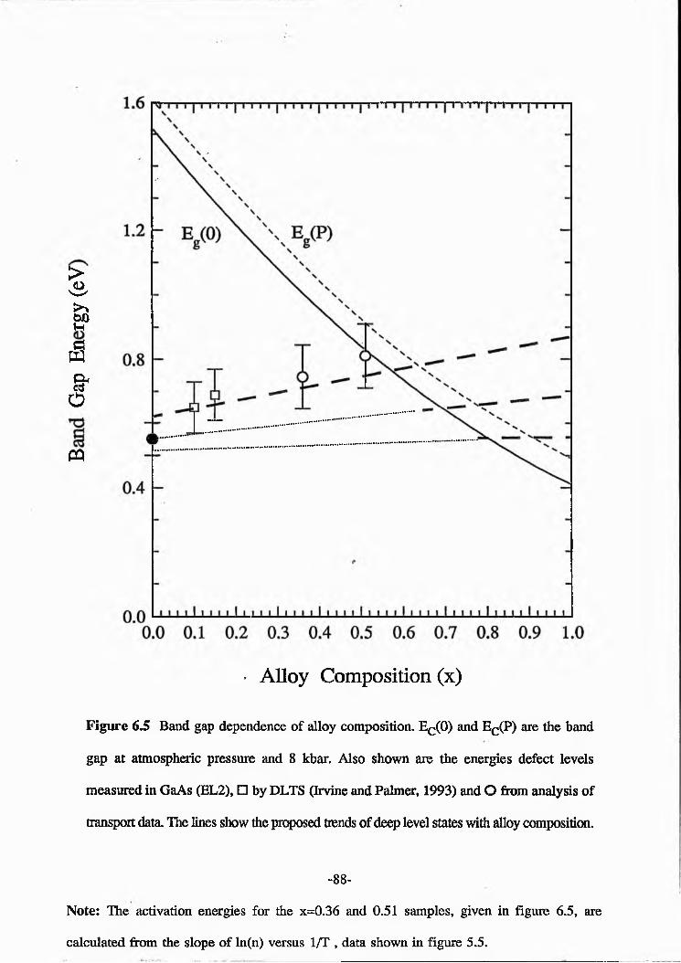
%>>bJ)fnd
Wcle f
0
CQ
• A l l o y C o m p o s i t i o n ( x )
Figure 6.5 Band gap dependence of alloy composition. Ec (0) and EC(P) are the band
gap at atmospheric pressure and 8 kbar. Also shown are the energies defect levels
measured in GaAs (EL2), □ by DLTS (Irvine and Palmer, 1993) and O from analysis of
transport data. The lines show the proposed trends of deep level states with alloy composition.
-88-
Note: The activation energies for the x=0.36 and 0.51 samples, given in figure 6.5, are
calculated from the slope of ln(n) versus 1/T , data shown in figure 5.5.
that there is no effective deep impurity levels. For the x=0.09 sample, below 50K, the
pressure dependence of carrier concentration rapidly increases with decreasing
temperature while the pressure dependence of carrier concentration for the x=0.20 starts
to increase just below 100K. This is because by decreasing temperature some shallow
levels become considerable compared to kT, so that the electron trap out to them
increases with decreasing temperature. However, the energy of such a level for the
x=0.20 sample is slightly higher than the x=0.09 sample. At low temperatures the
pressure dependence of carrier concentration is complicated by the carrier transfer and
overlap between impurity centres.
For the sample shown the opposite mobility/carrier concentration relation, in the
limited alloy composition 0.51<x<0.90, the two important features are observed from
the pressure dependence of carrier concentration at high temperatures. The first of these
is the increase in the room-temperature pressure dependence of carrier concentration with
decreasing alloy composition (x). The second is the increase in the pressure dependence
of carrier concentration with decreasing temperature as x is decreased toward x=0.51.
This high temperature behaviour of the pressure dependence of carrier concentration with
alloy composition (x) suggests that the generated deep levels in the band gap approaches
to the conduction band with increasing x, and enter into the conduction band at x«0.72.
At the In composition x=0.90, these levels fall just below the conduction band edge with
application of pressure up to 8 kbar. For the x=0.51 sample, the variation of pressure
dependence of carrier concentration with temperature also suggests that the presence of
two set of deep impurity levels in the band gap.
The pressure dependence of carrier concentration for the x=0.99 sample is consider
ably increased, with respect to the x<0.20 samples, and starts to increase with decreasing
temperature just below room-temperature. However, its pressure dependence of carrier
concentration is very small than the 0.20<x<0.90 samples. This is because the levels in
the conduction band have high energy to play an insignificant role with temperature and
pressure. Therefore, we expect the pressure dependence of mobility to be slightly
affected by these levels with decreasing temperature.
As a result of both dependence of mobility and carrier concentration on the alloy
composition (x), discussed in the previous chapter, and the pressure dependence of
mobility and carrier concentration across the alloy composition (x), a model involving
deep impurity levels from the relaxation of the epitaxial I i^ G a^ A s layer can be
proposed as follows. This is also shown in figure 6.5. For x<0.20 relaxation results in
only a small number of deep levels within the band gap. For 0.30<x<0.70 relaxation
results in many deep levels with in the band gap while for x>0.70 relaxation results in
an increased number of deep levels but these are now degenerate with the conduction
band.
We can now discuss the temperature dependence of mobility at pressures of ~4 kbar
and ~8 kbar in the light of the pressure dependence of carrier concentration and the deep
levels shown in figure 6.5. Figure 6.6, 6.7 and 6.8 show the temperature dependence of
mobility at the pressures indicated in the figures. The lines show the theoretical mobility
predicted by the ISBE using the measured carrier concentration and the pressure
dependence of material parameters discussed in chapter 2.
For the x=0.09 and 0.20 samples the theoretical mobilities calculated by the ISBE are
in excellent agreement with the experimental mobilities at the pressures as can be seen
in figure 6.6 and 6.7. For the x=0.09 sample, in the calculation for 3.5 kbar the
compensation ratio used was the atmospheric pressure value because of the nearly
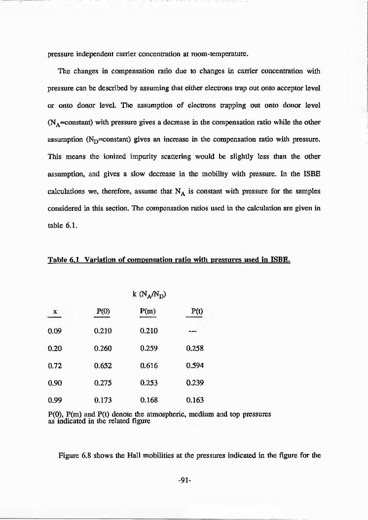
The changes in compensation ratio due to changes in carrier concentration with
pressure can be described by assuming that either electrons trap out onto acceptor level
or onto donor level. The assumption of electrons trapping out onto donor level
(NA=constant) with pressure gives a decrease in the compensation ratio while the other
assumption (ND=constant) gives an increase in the compensation ratio with pressure.
This means the ionized impurity scattering would be slightly less than the other
assumption, and gives a slow decrease in the mobility with pressure. In the ISBE
calculations we, therefore, assume that NA is constant with pressure for the samples
considered in this section. The compensation ratios used in the calculation are given in
table 6.1.
Table 6.1 Variation of compensation ratio with pressures used in ISBE.
pressure independent carrier concentration at room-temperature.
k (Na/Nd )
X P(0) P(m) P(t)
0.09 0.210 0.210 —
0.20 0.260 0.259 0.258
0.72 0.652 0.616 0.594
0.90 0.275 0.253 0.239
0.99 0.173 0.168 0.163
P(0), P(m) and P(t) denote the atmospheric, medium and top pressures as indicated in the related figure
Figure 6.8 shows the Hall mobilities at the pressures indicated in the figure for the
-91-
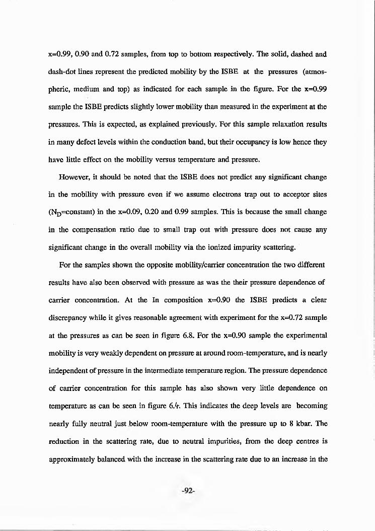
x=0.99, 0.90 and 0.72 samples, from top to bottom respectively. The solid, dashed and
dash-dot lines represent the predicted mobility by the ISBE at the pressures (atmos
pheric, medium and top) as indicated for each sample in the figure. For the x=0.99
sample the ISBE predicts slightly lower mobility than measured in the experiment at the
pressures. This is expected, as explained previously. For this sample relaxation results
in many defect levels within the conduction band, but their occupancy is low hence they
have little effect on the mobility versus temperature and pressure.
However, it should be noted that the ISBE does not predict any significant change
in the mobility with pressure even if we assume electrons trap out to acceptor sites
(ND=constant) in the x=0.09, 0.20 and 0.99 samples. This is because the small change
in the compensation ratio due to small trap out with pressure does not cause any
significant change in the overall mobility via the ionized impurity scattering.
For the samples shown the opposite mobility/carrier concentration the two different
results have also been observed with pressure as was the their pressure dependence of
carrier concentration. At the In composition x=0.90 the ISBE predicts a clear
discrepancy while it gives reasonable agreement with experiment for the x=0.72 sample
at the pressures as can be seen in figure 6.8. For the x=0.90 sample the experimental
mobility is very weakly dependent on pressure at around room-temperature, and is nearly
independent of pressure in the intermediate temperature region. The pressure dependence
of carrier concentration for this sample has also shown very little dependence on
temperature as can be seen in figure 6M This indicates the deep levels are becoming
nearly fully neutral just below room-temperature with the pressure up to 8 kbar. The
reduction in the scattering rate, due to neutral impurities, from the deep centres is
approximately balanced with the increase in the scattering rate due to an increase in the
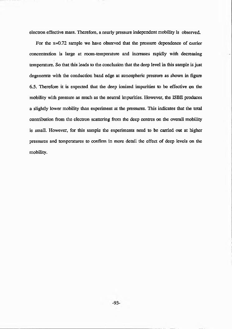
electron effective mass. Therefore, a nearly pressure independent mobility is observed.
For the x=0.72 sample we have observed that the pressure dependence of carrier
concentration is large at room-temperature and increases rapidly with decreasing
temperature. So that this leads to the conclusion that the deep level in this sample is just
degenerate with the conduction band edge at atmospheric pressure as shown in figure
6.5. Therefore it is expected that the deep ionized impurities to be effective on the
mobility with pressure as much as the neutral impurities. However, the ISBE produces
a slightly lower mobility than experiment at the pressures. This indicates that the total
contribution from the electron scattering from the deep centres on the overall mobility
is small. However, for this sample the experiments need to be carried out at higher
pressures and temperatures to confirm in more detail the effect of deep levels on the
mobility.
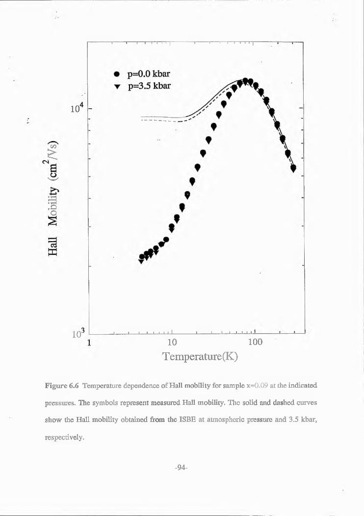
T----- 1----1---1--I I I I | t------1--- 1—i—i—t—r—rj
GO£W
a• 8
10
1 0 ; I I I__I_1_L—L-L-l. J_______l l l l l l I
1 0 1 0 0
T e m p e r a t u r e ( K )
Figure 6.6 Temperature dependence of Hall mobility for sample x=0.09 at the indicated
pressures. The symbols represent measured Hall mobility. The solid and dashed curves
show the Hall mobility obtained from the ISBE at atmospheric pressure and 3.5 kbar,
respectively.
-94-
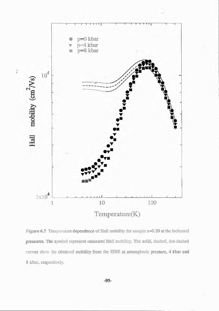
l ( f -
2x10
i p - 0 kbar t p = 4 kbar ■ p - 8 kbar
■■ ■
I 1 I I I I
1 10 100
T e m p e r a t u r e ( K )
Figure 6.7 Temperature dependence of Hall mobility for sample x=0.20 at the indicated
pressures. The symbol represent measured Hall mobility. The solid, dashed, dot-dashed
curves show the obtained mobility from the ISBE at atmospheric pressure, 4 kbar and
8 kbar, respectively.
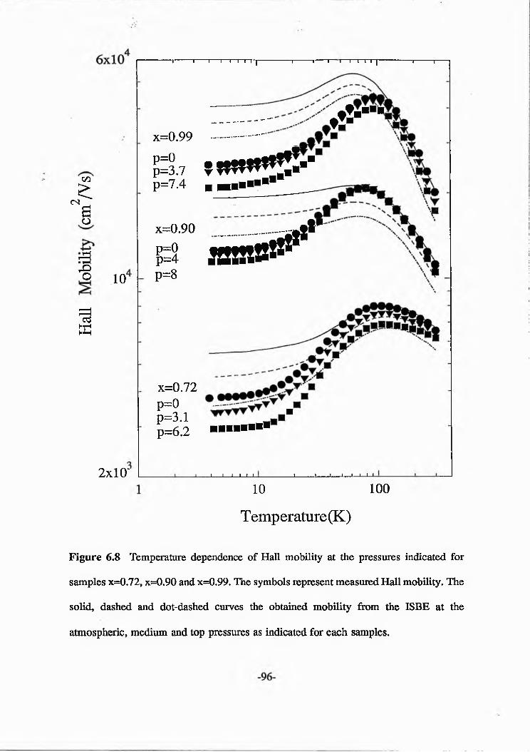
i i i i i i i r~|------------ 1-------1---- 1 i i i i i |------------ 1-------r
f t
00
IO
r 3x>o
3EC
10
2 x l 0 ‘
/ * * r
* = ° " - ........
^ .7 * sw * ’! ! ! '1p=7.4 B « « ■ ■ ■ ■ ■
x=0.90 ^ j j t V
p s s a a a * * ^p = 8
x=0.72
p = 0 ■ p=3.1p=6.2 ■ ■ ■ ■ ■ ■ ■ *
..1 I I I 1 LO- j ________ t I i i i r i
10 100
T e m p e r a t u r e ( K )
Figure 6.8 Temperature dependence of Hall mobility at the pressures indicated for
samples x=0.72, x=0.90 and x=0.99. The symbols represent measured Hall mobility. The
solid, dashed and dot-dashed curves the obtained mobility from the ISBE at the
atmospheric, medium and top pressures as indicated for each samples.
6 . 4 T e m p e r a t u r e a n d P r e s s u r e D e p e n d e n c e o f M o b i l i t y a n d
C a r r i e r C o n c e n t r a t i o n i n t h e x = 0 . 5 1 a n d 0 . 6 0 S a m p l e s
Figure 6.9 shows the room-temperature normalised pressure dependence of Hall
mobility (closed symbols) and carrier concentration (open symbols) for the x=0.51 and
two InQ 6oGao 40As samples. Both carrier concentration and mobility show a stronger
decrease with increasing pressure than the other Ii^ G a^A s samples. The changes in
growth temperature do not affect the pressure dependence of mobility and carrier
concentration strongly, as can be seen in the figure. However, the x=0.6 sample which
was grown at 430°C shows a slightly stronger dependence on pressure than the sample
grown at 480°C. The x=0.51 sample is more sensitive to pressure than the x=0.60
samples as can be seen in the figure. This is consistent with the level being deeper in
this sample than in the x=0.60 samples.
The temperature dependence of carrier concentration for the x=0.51 and 0.60 samples
at three pressures are given in figure 6.10. It is clear that in the x=0.60 sample the
carrier concentration is higher than in the x=0.51, and its pressure dependence is also
smaller than the other sample. For the x=0.51, at the highest pressure the carrier
concentration tends to decrease below 100K while it tends to a constant with decreasing
temperature at atmospheric pressure. This suggests that a second impurity level appears
in the band gap at pressure ~7.4 kbar. However, there is no evidence for the second
impurity level in the x=0.60 sample. Therefore, it is expected that a strong effect on the
mobility from ionized deep donors in the x=0.51 sample.
The temperature dependence of the Hall mobility for the x=0.51 and 0.60 is given
No
rmal
ized
H
all
Mob
ilit
y an
d C
arri
er
Co
nc
en
tra
tio
n
P r e s s u r e ( k b a r )
Figure 6.9 The 300K normalised pressure dependence of Hall mobility (closed
symbols) and carrier concentration (open symbols) for the x=0.51 and 0.60 samples.
-98-
Ha
ll C
arri
er
Co
nce
ntr
atio
n
(cm
)1 1— i—i—i—p
1 0 1 6 1- * , 0 : 0 k b a r O H, v : 4 k b a r: 7 . 4 , □ : 8 k b a r ° 9
O v °
° g p O T 9 U
om d *
o
t o 15
ow □
O v ^• v P j ,
O
V
VV
V
■H
_i______ i____ i___ i__ i__i—i—1~
10 1 00
T e m p e r a t u r e ( T )
Figure 6.10 Temperature dependence of carrier concentration at the pressures indicated
for the x=0.60 (Tgr=480°C, open symbols) and x=0.51 (Tgr=530°C, closed symbols)
samples.
CN
C/3
i>BCJ
f f i
T e m p e r a t u r e ( K )
Figure 6.11 Temperature dependence of Hall mobility at the pressures indicated for the
x=0.51; (a) and x=0.60; (b) samples. The symbols represent measured Hall mobility. The
curves show the Hall mobility obtained from the ISBE at the related pressures, with the
usual notation. The bold lines show the mobility limited by an additional scattering
mechanism for the same pressures as the ISBE mobility. For the additional scattering
mechanisms (i~T2 , 6 at the atmospheric pressure as in table 5.3.
- 1 0 0 -
in figure 6.11. The symbols represent the experimental data as usual. The lines show the
ISBE calculations assuming electrons trap out to acceptor sites. The compensation ratios
used in the calculations are also given in the table 6 .2 . As can clearly be seen in the
figure neither an agreement with the temperature nor with pressure dependence of
mobility can be achieved using the ISBE with the Brooks-Herring model of ionized
impurity scattering. The ISBE only gives a poor agreement at just around room-
temperature using the high compensation ratios at the pressures, and with decreasing
temperature the experimental mobility at the pressures decreases very much faster than
those predicted by the ISBE.
Table 6.2 Compensation ratios at the pressures for samples shown in figure 6.11.
k (Na/Nd)
X Tg(±20°C) P(0) P(m) P(t)
0.51 530 0.978 0.983 0.989
0.60 480 0.980 0.985 0.987
The large discrepancy between the ISBE calculation and experiment can be explained
by considering a number of deep levels in the band gap. For the x=0.51, firstly the
strong trap out with temperature suggests that the deep level is effective even at low
temperatures (-70K), the ionization of deep centres starts around this temperature.
Secondly, at the highest pressure a rapid and continuously decrease in carrier
concentration with temperature also suggests the presence of a large number of ionized
deep centres down to temperatures of 50K even at high pressures. This also suggests
there may be a continuum of deep levels. Therefore, the electron scattering from the
deep centres reduces the mobility with decreasing temperature even at high pressures,
up to 8 kbar.
However, an additional scattering mechanism having an effective temperature
dependence of ~T2 , 6 has been found at atmospheric pressure in the previous chapter. If
such a scattering mechanism is associated with the deep centres, its temperature and
pressure dependence should be dependent on the change of the density of ionized deep
donors with temperature and pressure. We find using a Matthiessens rule approach that
the additional mechanism has a temperature dependence of T3 , 3 and T3 , 8 at 4 and 7.4
kbar, respectively, as shown in figure 6 .Il.a. These values are close to the experimental
dependence on temperature. This suggests that the electron scattering from the ionized
deep centres is very effective even at low temperatures and high pressures. Alternatively,
at high pressures a strong neutral impurity scattering may be raised up by the large
number of neutral impurities with decreasing temperature. It should be noted that the
pressure dependence of mobility for the x=0.51 sample increases faster with decreasing
temperature than the x=0.60 sample. For the x=0.6 sample an additional scattering
mechanism has a T2 - 9 dependence at 4 kbar, as shown in figure 6 .Il.b. For this sample
the effect of deep levels on electron transport is weaker than the x=0 .5 0 .
6 . 5 C o n c l u s i o n s
The mobility in Si-doped relaxed InxGa1-xAs grown on GaAs substrate by MBE has
been measured and both temperature and pressure dependence of mobility were
calculated using an ISBE, including the relevant scattering mechanisms. Both the
- 1 0 2 -
measured temperature and pressure dependence of mobility together with an ISBE
calculations have shown that the dependence of mobility on In composition is
characterized by pronounced ionized impurity scattering and that the electron scattering
from the deep centres, which is connected with crystal defects, layer relaxation and the
Si-doping density, particularly as alloy composition approaches x~0.40.
Both the measured temperature and pressure dependence of carrier concentration have
also shown that the dependence of carrier concentration on the alloy composition (x) is
linked to the deep levels. For the x<0.20 relaxation results in only a small number of
deep levels so that a negligible effect on the electron transport has been observed. In this
alloy composition range, the standard model ISBE is in good agreement with both the
experimental temperature and pressure dependence of mobility. For 0.30<x<0.60
relaxation results in many deep levels within the band gap which trap out electrons
resulting in low carrier density, low mobility material. The ISBE fails to predict both
temperature and pressure dependence of mobility in this alloy composition range.
However, for x>0.60 relaxation results in many deep levels but they appear degenerate
with the conduction band and hence have litde effect on the observed electron transport.
The standard model is in good agreement with the temperature dependence of mobility
but, it does not give a good agreement with the pressure dependence of mobility.
C h a p t e r 7
I m p u r i t y C o n d u c t i o n i n I n x G a 1 ;;A s
7 .1 I n t r o d u c t i o n
In the previous chapters we have shown that an ISBE can be used to successfully
predict the temperature and pressure dependence of mobility over a wide temperature
range, when the electron scattering from deep centres is negligible. However, the ISBE
fails to predict the temperature and pressure dependence of mobility at low temperatures
where impurity conduction occurs. To account for the inadequacy of the modelling of
electron scattering in the conduction band using an ISBE we, therefore, study the
impurity conduction phenomenon in L^Ga^As at low temperatures. However, we
prefer to discuss the temperature dependence of resistivity (conductivity) instead of the
mobility. The main evidence that the impurity conduction is occurring at low
temperatures is the observed minimum in the carrier concentration and the low and
approximately constant mobility at low temperatures. The presence of a minimum in the
temperature dependence of carrier concentration has also been used as evidence of
impurity conduction by several authors, [Emel’yanenko et al., 1965, Mott and Davis,
1971, and Molnar et al., 1993].
According to the Mott criteria, [Mott and Twose, 1961], there are two different
mechanisms for impurity conduction depending on the degree of overlap between donor
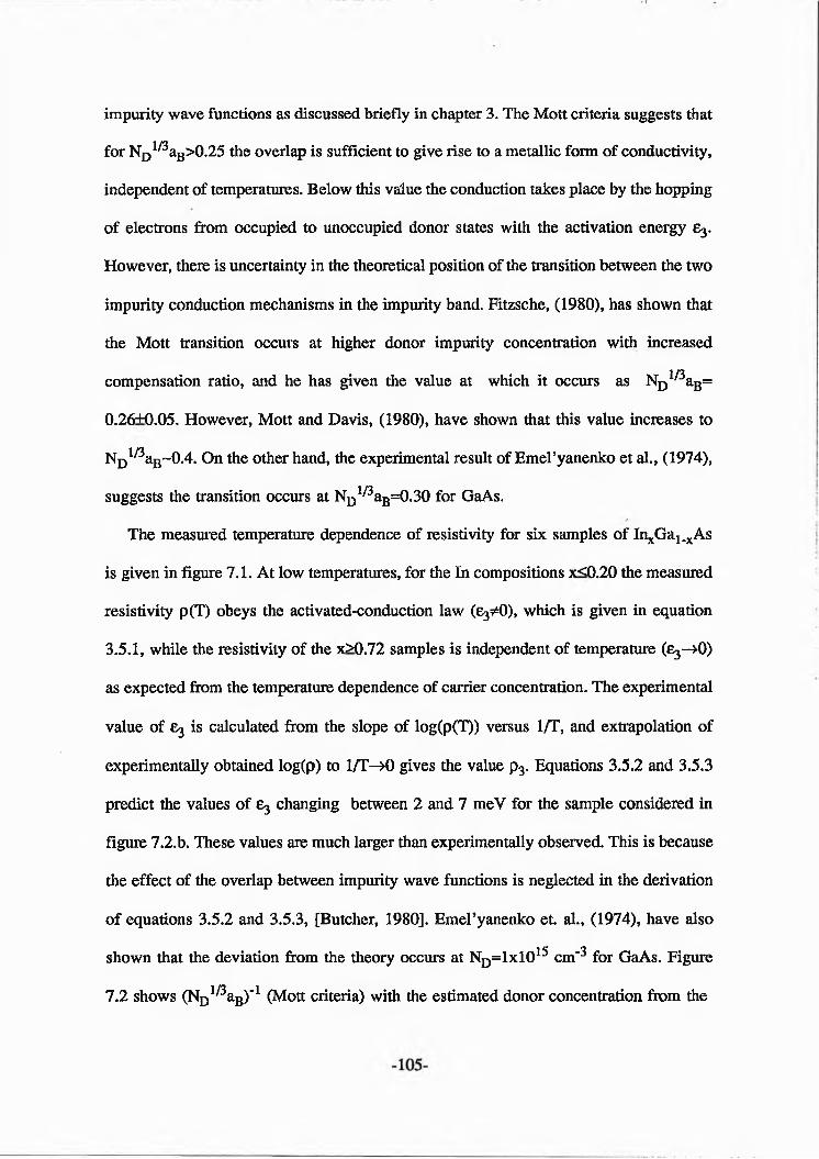
impurity wave functions as discussed briefly in chapter 3. The Mott criteria suggests that
for ND1/3aB>0.25 the overlap is sufficient to give rise to a metallic form of conductivity,
independent of temperatures. Below this value the conduction takes place by the hopping
of electrons from occupied to unoccupied donor states with the activation energy 6 3 .
However, there is uncertainty in the theoretical position of the transition between the two
impurity conduction mechanisms in the impurity band. Fitzsche, (1980), has shown that
the Mott transition occurs at higher donor impurity concentration with increased
compensation ratio, and he has given the value at which it occurs as NDly3 aB=
0.26+0.05. However, Mott and Davis, (1980), have shown that this value increases to
ND1 ^aB~0.4. On the other hand, the experimental result of Emel’yanenko et al., (1974),
suggests the transition occurs at NDli/3aB=0.30 for GaAs.
The measured temperature dependence of resistivity for six samples of fr^Ga^As
is given in figure 7.1. At low temperatures, for the In compositions x<0.20 the measured
resistivity p(T) obeys the activated-conduction law (£3 5 *0 ), which is given in equation
3.5.1, while the resistivity of the x>0.72 samples is independent of temperature (£3 —>0)
as expected from the temperature dependence of carrier concentration. The experimental
value of £ 3 is calculated from the slope of log(p(T)) versus 1/T, and extrapolation of
experimentally obtained log(p) to 1/T—>0 gives the value p3. Equations 3.5.2 and 3.5.3
predict the values of £ 3 changing between 2 and 7 meV for the sample considered in
figure 7.2.b. These values are much larger than experimentally observed. This is because
the effect of the overlap between impurity wave functions is neglected in the derivation
of equations 3.5.2 and 3.5.3, [Butcher, 1980]. Emel’yanenko et. al., (1974), have also
shown that the deviation from the theory occurs at Nd=1x1015 cm" 3 for GaAs. Figure
7.2 shows (Np^a ^ - 1 (Mott criteria) with the estimated donor concentration from the
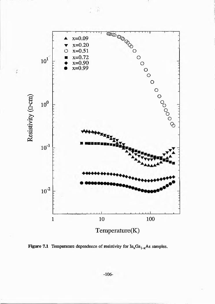
Re
sist
ivit
y (O
cm
)
i o 1
1 0°
10"1
1 0 '2
l 10 t o o
T e m p e r a t u r e ( K )
Figure 7.1 Temperature dependence of resistivity for In^Ga^As samples.
a x = 0 .0 9 ▼ x = 0 .2 0 O x = 0 .5 1 ■ x = 0 .7 2♦ x = 0 .9 0• x = 0 .9 9
<®a>1------1----1---1--1--1"'I T |
oooooooo°oooo
9 )
X x■ ■ ■ ■ ■ ■ ■ ■ ■ ■
J___ I__ I__1_I_1_I I. I J___ I__ I__I—I—I—1-1.- ___ I
A l l o y C o m p o s i t i o n ( x )
Figure 7.2 (a); l/(ND) 1 3̂ aB and (b); activation energy versus alloy composition (x). The
solid triangle for GaAs with n=1.05xl016 cm' 3 from Basinski and Olivier (1967).
-1 0 7 -
ISBE and experimentally observed activation energy £ 3 versus alloy composition (x). As
can be seen from figure 7.2, (ND1 /3 aB ) _ 1 decreased at high In concentrations because of
the increased donor concentration and an increase in Bohr radius aB with increasing
alloy composition. This is confirmed by the composition dependence of activation
energy. A complete overlap of impurity states between themselves and the conduction
band occurs at ND>2xl01 6 cm- 3 and x>0.51: In this range the activation energy 6 3
tends to zero. Therefore, it is assumed that the x<0.20 samples are close to the Mott
transition in the thermally activated regime, and the x>0.51 samples are close to the
transition but on the metallic side of it. So that, the transition may occur near the middle
of the composition of In^Ga^As system. We, therefore, analyse the low temperature
resistivity in terms of the thermally-activated hopping conduction for x<0 . 2 0 and in
terms of the metallic conduction for x>0.51.
7 . 2 I m p u r i t y C o n d u c t i o n a t x < 0 . 2 0
In this section, we analyse the low temperature resistivity measurements using
equation 3.5.1. The pressure dependence of resistivity enters in equation 3.5.1 through
the resistivity p3; which is given in equation 3.5.4, via the effective Bohr radius and p0
given by equation 3.5.5. The required parameters for the calculation were worked out
from table 2.1 by interpolation. In the calculation, we have used the measured £ 3 values
with pressure because the deviation of the measured £ 3 from the theory for large ND as
a result of the overlap of the impurity wave functions. However, we could not find any
clear differences in the activation energy £ 3 at the pressures in the resolution of
experiment. It is assumed that a is independent of pressure which is reasonable as the
-1 0 8 -
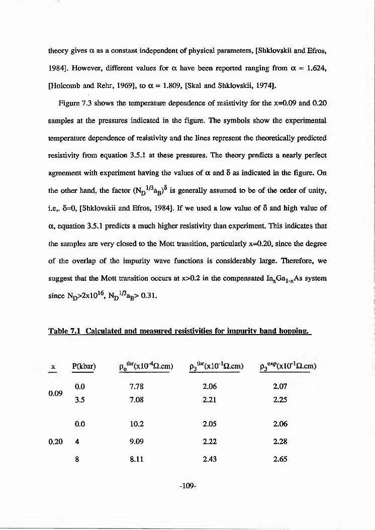
theory gives a as a constant independent of physical parameters, [Shklovskii and Efros,
1984]. However, different values for a have been reported ranging from a = 1.624,
[Holcomb and Rehr, 1969], to a = 1.809, [Skal and Shklovskii, 1974].
Figure 7.3 shows the temperature dependence of resistivity for the x=0.09 and 0.20
samples at the pressures indicated in the figure. The symbols show the experimental
temperature dependence of resistivity and the lines represent the theoretically predicted
resistivity from equation 3.5.1 at these pressures. The theory predicts a nearly perfect
agreement with experiment having the values of a and 8 as indicated in the figure. On
the other hand, the factor (ND^3 aB ) 5 is generally assumed to be of the order of unity,
i.e,. 8=0, [Shklovskii and Efros, 1984]. If we used a low value of 8 and high value of
a, equation 3.5.1 predicts a much higher resistivity than experiment. This indicates that
the samples are very closed to the Mott transition, particularly x=0.20, since the degree
of the overlap of the impurity wave functions is considerably large. Therefore, we
suggest that the Mott transition occurs at x>0.2 in the compensated I^G a^As system
since ND>2xl016, ND1/3 aB> 0.31.
Table 7.1 Calculated and measured resistivities for impurity band hopping.
X P(kbar) p^CxlO^Q.cm) p3 thr(xlO'1 Q.cm) p3 exp(xl 0 '
0 . 0 7.78 2.06 2.070.09
3.5 7.08 2 . 2 1 2.25
0 . 0 1 0 . 2 2.05 2.06
0 . 2 0 4 9.09 2 . 2 2 2.28
8 8 . 1 1 2.43 2.65
-1 0 9 -
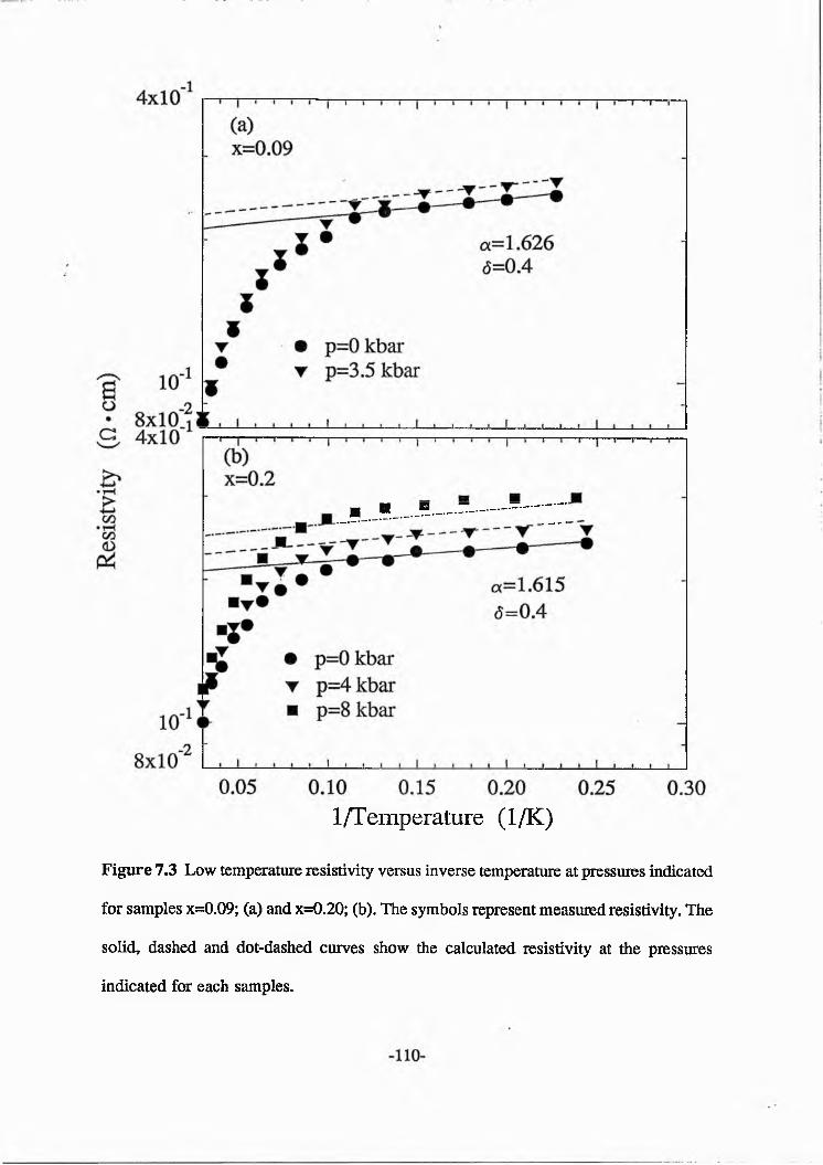
1 / T e m p e r a t u r e ( 1 / K )
Figure 7.3 Low temperature resistivity versus inverse temperature at pressures indicated
for samples x=0.09; (a) and x=0.20; (b). The symbols represent measured resistivity. The
solid, dashed and dot-dashed curves show the calculated resistivity at the pressures
indicated for each samples.
The theory predicts a slightly lower resistivity than experiment at 8 kbar as can be
seen from the figure. This suggests that the overlap between impurity wave functions is
more less than predicted from equation 3.5.1, and this increases the hopping resistivity.
However, we give in more detail the measured and predicted p3 and p0 values in table
7.1. It is clear that both theory and experiment show an increase in the resistivity p3 but
the theory predicts slightly lower increases than observed experimentally. It is expected
that the reduction in the overlap due to pressure not only affects p3 but also increases
activation energy 6 3 . However, we did not observe any considerably increase in 6 3 .
There are a number of possible reasons for the small disagreement between experimental
and theoretical pressure dependence of resistivity. The first uncertainty is that in the
estimation of ND by fitting the ISBE to high temperature Hall mobility results. The
second uncertainty is that in the estimation of ND under pressure. We assume electron
trap out to donor sites. However, there may be an error in the experimental resistivity
p3 and activation energy e3 because of the resolution of experiment. We, therefore,
conclude that the agreement between theory and experiment is very good even though
there is uncertainty in ND and an experimental error.
The calculated pG values decrease with pressure as can be seen in table 7.1, since
Bohr radius aB decreases more significantly than the other parameters. Both p3 and pc
stay constant with temperature up to 50K because the effective mass m* and the
dielectric constant es are virtually constant at low temperatures. It should be noted that
in the literature p0 has widely been studied experimentally as a function of ND, and the
reported value of p0 ranges from lxlO " 4 to 8X10"4 O.cm depending on donor
concentration for GaAs, [Shklovskii and Efros, 1984].
7 . 3 I m p u r i t y C o n d u c t i o n a t x > 0 . 5 0
In this section we discuss the low temperature resistivity measurements for the
x>0.72 samples. The conductivity for these samples is formally closer to metallic than
thermally-activated hopping as discussed previously. The theory of the conductivity in
the vicinity of the critical region (Mott transition) is not yet well understood. However,
there are many investigations on the conductivity near the critical region in the literature.
A general review on the behaviour of conductivity in the vicinity of Mott transition has
been given by Mott, (1990).
Thomas, (1985), has shown that for silicon at low temperatures the conductivity
behaves like
o =oo (Nd-N0) '’ 7 .3 . 1
with v=0.5, and Nc is the critical density at which the transition occurs. Experimentally,
the work of Paalanen et al., (1982), gives
< ^ - 1 >V 7 - 3 ‘ 2
where grtlin is the minimum metallic conductivity. Katsumato et al., (1987), investigated
the low temperature conductivity in AlQ 3 Ga0 7As doped with silicon. They showed that
the conductivity behaves like
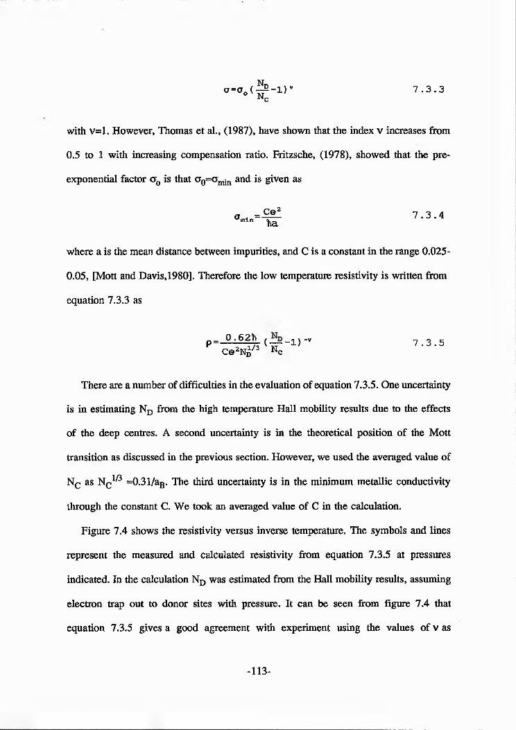
o=o 0 ( ^ - l ) » 7 . 3 . 3Nc
with v=l. However, Thomas et al., (1987), have shown that the index v increases from
0.5 to 1 with increasing compensation ratio. Fritzsche, (1978), showed that the pre
exponential factor a 0 is that rto=°min an(l Is given as
a „ln= -2®1 7 . 3 . 4t e
where a is the mean distance between impurities, and C is a constant in the range 0.025-
0.05, [Mott and Davis, 1980]. Therefore the low temperature resistivity is written from
equation 7.3.3 as
p= ° ' 6 2 1 l < v ~ 1 ) ' V 7 . 3 . 5Ce 2 ND7 Nc
There are a number of difficulties in the evaluation of equation 7.3.5. One uncertainty
is in estimating ND from the high temperature Hall mobility results due to the effects
of the deep centres. A second uncertainty is in the theoretical position of the Mott
transition as discussed in the previous section. However, we used the averaged value of
Nc as Nc ^ =0.31/aB. The third uncertainty is in the minimum metallic conductivity
through the constant C. We took an averaged value of C in the calculation.
Figure 7.4 shows the resistivity versus inverse temperature. The symbols and lines
represent the measured and calculated resistivity from equation 7.3.5 at pressures
indicated. In the calculation ND was estimated from the Hall mobility results, assuming
electron trap out to donor sites with pressure. It can be seen from figure 7.4 that
equation 7.3.5 gives a good agreement with experiment using the values of v as
-1 1 3 -
ao
34—»• r-(>00• rH00CD
P4
x = 0 .7 22/=0.5
p = 6 .2 k b a r
p = 3 .1 k b a r
p = 0 k b a r
x = 0 .9 0i/ = 0 .5 6
p = 8 k b a r p = 4 k b a r p = 0 k b a r
x = 0 .9 9 17=0.71
p = 7 .4 k b a r p = 3 .7 k b a r p = 0 k b a r
0 .1 0 .2 0 .3
1 / T e m p e r a t u r e ( 1 / K )
Figure 7.4 Low temperature resistivity versus inverse temperature at the pressures
indicated for samples x=0.72, x=0.90 and x=0.99. The symbols represent measured
resistivity. The solid, dashed and dot-dashed curves show the calculated resistivity at
atmospheric, medium and top pressures as indicated for each samples.
-1 1 4 -
indicated in the figure at the atmospheric pressure. However, for the In composition
x=0.72 equation 7.3.5 requires a lower value of V (-0.4). This may be due to a large
error in the estimated ND from the ISBE. We find good agreement with experiment
using the measured carrier concentration instead of ND as can be seen in the figure. This
approach has also been used by Biskupski, (1984), and Long and Pepper, (1984), to
explain the low temperature resistivity for InP and InSb.
Equation 7.3.5 produces remarkably good agreement with the experimental
temperature dependence of resistivity at the various pressures, making a number of
assumptions, despite the fact that samples are far away from the Mott transition with
increasing In content. It is found that the critical exponent of transition v decreases with
decreasing alloy composition (x) and therefore with the increasing compensation ratio
and approaching the Mott transition. This is contrast to the result of Thomas et al.,
(1987). They found the critical exponent v increases with increasing compensation ratio
for silicon.
The x=0.51 sample shows a strong increase in the resistivity at high temperatures
due to the strong effect of the deep centres. We do not attempt to analyse the low
temperature resistivity for this sample due to a large error in the ND estimated from Hall
mobility analysis using the ISBE. However, the measurement could also be made down
to a temperature of 14K for this sample.
7 . 4 C o n c l u s i o n s
We have shown that the Mott transition occurs in the limited alloy composition range
x=0.30-0.50 in Si doped I^G a^A s for a particular lx l0 1 6 cm' 3 of doping density. The
-115-
temperature and pressure dependence of the low temperature resistivity can be well
explained in terms of a thermally-activated hopping conduction law at x<0.20. For the
In compositions x>0.72 the low temperature resistivity is defined by equation 7.3.5. It
is found that the critical exponent v decreases with increasing compensation ratio in the
metallic regime for the limited alloy composition x>0.72.
C h a p t e r 8
C o n c l u s i o n s a n d R e c o m m e n d a t i o n s f o r
F u r t h e r W o r k
In this thesis the electron mobility in relaxed In^Ga^As grown on GaAs by MBE
with n~101 6 cm "3 has been investigated as a function of temperature (4.2-300K) and
pressure (0-8 kbar). The individual scattering mechanisms have different dependencies
on the electron effective mass (m*) and temperature, thus the comparison of experimen
tal and theoretical mobility results as a function of pressure and temperature has allowed
the dominant scattering mechanisms to be identified in the samples examined.
A dramatic decrease in both the mobility and carrier concentration in a limited alloy
composition range, x=0.30-0.60, has been observed. It has been shown that the measured
mobility in Ii^Ga^As can be well described by modelling electron scattering in both
the conduction band and via a donor impurity band for a large alloy composition range.
The investigation of electron mobility in I^G a^A s has shown that an iterative
solution of the Boltzmann equation (ISBE) including most of the relevant scattering
mechanisms is in good agreement with experiment over a wide temperature range.
However, both the measured temperature and pressure dependence of mobility and the
ISBE calculations have shown that the dependence of mobility on the alloy composition
(x) is characterized by pronounced ionized impurity scattering and electron scattering
from the deep centres as alloy composition (x) approaches x~0.40. For the x=0,51 and
0.60 layers an additional scattering mechanism having an effective temperature
dependence ~T2,6 has been observed and this is thought to be associated with the deep
centres.
Both the measured temperature and pressure dependence of carrier concentration have
also shown that the dependence of carrier concentration on the alloy composition (x) is
linked to the deep levels associated with layer relaxation and generation of crystal
defects. Deep defect levels are responsible for both loss of carriers from the conduction
band and the large temperature and pressure dependence of carrier concentration in the
middle of the alloy composition range.
The standard model ISBE fails to predict both the temperature and pressure
dependence of mobility at low temperatures where impurity band conduction occurs. It
was necessary to consider the impurity conduction in addition to the standard model
ISBE at low temperatures. The resistivity analysis at low temperatures has shown that
the Mott transition occurs in the limited alloy composition range x=0.30 - 0.50 in
fr^Ga^As since ND>2xl016cm‘3 for a Si-doping concentration of 1016cm'3. The
temperature and pressure dependence of resistivity and consequently mobility can be
well described in the terms of impurity conduction at low temperatures.
A number of suggestions can be made for extensions to the work reported in this
thesis. The first of these is to examine the effect of deep levels on transport at higher
temperatures (300-500K) and pressures (up to 15 kbar). It would also be interesting to
investigate how the transport properties are modified for samples uniformly doped at
1015 and 1017 cm"3. This would allow further work on impurity scattering and impurity
band conduction to be made. Finally, as progress is made on controlling the distribution
of defects arising from layer relaxation measurements of the intrinsic electron transport
properties of Ir^Ga^As layers with x in the range 0.30-0.70 may become possible.
R e f e r e n c e s
Adachi E., (1968), J.Phys.Soc Japan 24,1178.
Adachi S., (1982), J.AppLPhys. 53,12,8775.
Adachi S. and Oe K.,(1984), J.Appl.Phys. 56,5,1494.
Adachi S., (1985), J.Appl.Phys. 58,3,R1.
Adachi S., (1992), in Physical Properties of III-V Semiconductor Compounds, (John
Willey and Sons New York Chichester Brisbane Toronto Singapore).
Allen L.C., (1955), Phys.Rev. 98,4,993.
Arlt G. and Quadflieg, (1968), Physica Status Solidi 25,1, 323.
Aspnes D.E., (1976), Phys.Rev. B14,12,S331.
Bardeen J. and Shocley W., (1950), Phys.Rev. 80,1,72.
Basinski J. and Olivier R., (1967), Can.J.Phys. 45,119.
Bateman T.B., McSkimin H.J. and Whelon J.M., (1959), J.AppLPhys. 30,4,544.
Benzaquen M. Walsh D. and Mazuruk K., (1987), Phys.Rev. B36,8,4388.
Benzaquen M, Walsh D., Beaudoin M., Mazuruk K. and Puetz N., (1988), J.Crystal
Growth 93,562.
Berolo O., Wooley J.C. and Van Vachten J.A., (1973), Phys.Rev. B8,8,3794.
Biskupski G„ Dubois H., Wojkiewicz, Briggs A. and Remenyi G., (1984), J.Phys.C 17,
L411.
Blakemore J.S., (1987), in Semiconductor Statistics (Dover Publications,INC. New
York).
Blood P. and Orton J.W., (1974), J.Phys. C7,893.
- 1 2 0 -
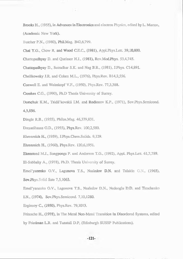
Brooks H., (1955), in Advances in Electronics and electron Physics, edited by L. Marton,
(Academic New York).
Butcher P.N., (1980), PhiLMag. B42,6,799.
Chai Y.G., Chow R. and Wood C.E.C., (1981), Appl.Phys.Lett. 39,10,800.
Chattopadhyay D. and Queisser H.J., (1981), Rev.Mod.Phys. 53,4,745.
Chattopadhyay D., Sutradhar S.K. and Nag B.R., (1981), J.Phys. 014,891.
Chelikowsky J.R. and Cohen M.L., (1976), Phys.Rev. B 14,2,556.
Conwell E. and Weisskopf V.F., (1950), Phys.Rev. 77,3,388.
Crookes C.G., (1990), Ph.D Thesis University of Surrey.
Demchuk K.M., TsidiFkovskii I.M. and Rodionov K.P., (1971), Sov.Phys.Semicond.
4,5,856.
Dingle R.B., (1955), Philos.Mag. 46,379,831.
Dresselhauss G.D., (1955), Phys.Rev. 100,2,580.
Ehrenreich H., (1959), J.Phys.Chem.Solids. 9,129.
Ehrenreich H., (1960), Phys.Rev. 120,6,1951.
Ekenstend M.J., Songpongs P. and Anderson T.G., (1992), Appl. Phys.Lett. 61,7,789.
El-Sabbahy A., (1978), Ph.D. Thesis University of Surrey.
EmeFyanenko O.V., Lagunova T.S., Nasledov D.N. and Talakin G.N., (1965),
Sov.Phys.Solid Sate 7,5,1063.
Emel’yanenko O.V., Lagonova T.S., Nasledov D.N., Nedeoglu D.D. and Timchenko
I.N., (1974), Sov.Phys.Semicond. 7,10,1280.
Erginsoy C., (1950), Phys.Rev. 79,1013.
Fritzsche H., (1978), in The Metal Non-Metal Transition In Disordered Systems, edited
by Friedman L.R. and Tunstall D.P, (Edinburgh SUSSP Publications).
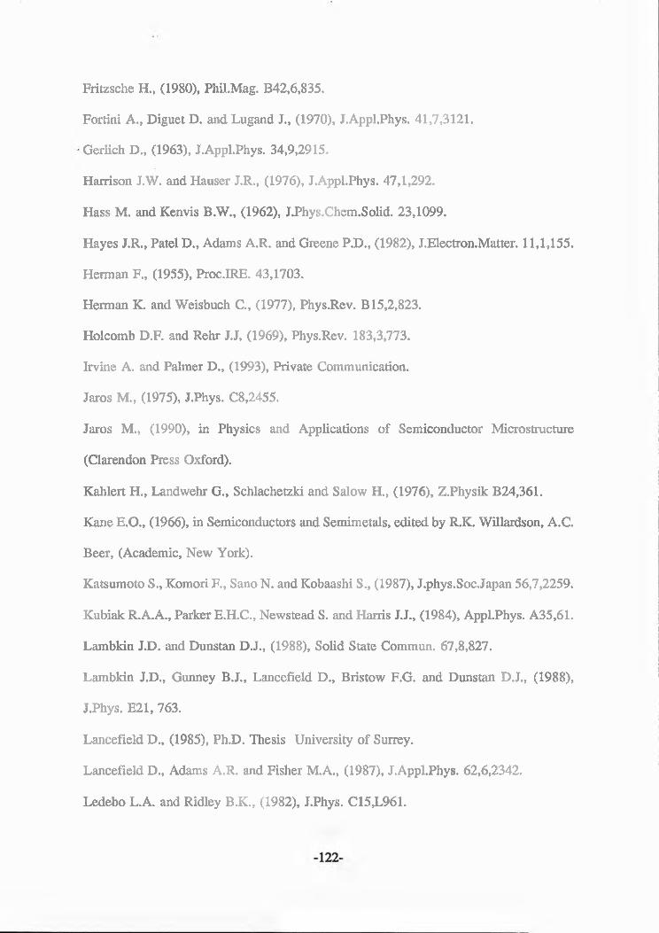
Fritzsche H., (1980), Phil.Mag. B42,6,835.
Fortini A., Diguet D. and Lugand J., (1970), J.Appl.Phys. 41,7,3121.
Gerlich D., (1963), J.Appl.Phys. 34,9,2915.
Harrison J.W. and Hauser J.R., (1976), J.Appl.Phys. 47,1,292.
Hass M. and Kenvis B.W., (1962), J.Phys.Chem.Solid. 23,1099.
Hayes J.R., Patel D., Adams A.R. and Greene P.D., (1982), J.Electron.Matter. 11,1,155.
Herman F., (1955), Proc.IRE. 43,1703.
Herman K. and Weisbuch C., (1977), Phys.Rev. B 15,2,823.
Holcomb D.F. and Rehr J.J, (1969), Phys.Rev. 183,3,773.
Irvine A. and Palmer D., (1993), Private Communication.
Jaros M., (1975), J.Phys. C8,2455.
Jaros M., (1990), in Physics and Applications of Semiconductor Microstructure
(Clarendon Press Oxford).
Kahlert H., Landwehr G., Schlachetzki and Salow H., (1976), Z.Physik B24.361.
Kane E.O., (1966), in Semiconductors and Semimetals, edited by R.K. Willardson, A.C.
Beer, (Academic, New York).
Katsumoto S., Komori F., Sano N. and Kobaashi S., (1987), J.phys. Soc Japan 56,7,2259.
Kubiak R.A.A., Parker E.H.C., Newstead S. and Harris J.J., (1984), AppLPhys. A35,61.
Lambkin J.D. and Dunstan D.J., (1988), Solid State Commun. 67,8,827.
Lambkin J.D., Gunney B.J., Lancefield D., Bristow F.G. and Dunstan D.J., (1988),
J.Phys. E21, 763.
Lancefield D., (1985), Ph.D. Thesis University of Surrey.
Lancefield D., Adams A.R. and Fisher M.A., (1987), J.AppLPhys. 62,6,2342.
Ledebo L.A. and Ridley B.K., (1982), J.Phys. C15,L961.
Littlejohn M.A., Hauser J.R, Glission T.H., Ferry D.K. and Harrison J.W., (1978),
Solid.Sate.Elect. 21,107.
Long A.P. and Pepper M., (1984), J.Phys. C17, 3391.
Look D.C., (1989), in Electrical Characterization of GaAs Materials and Devices, (John
Wiley and Sons Chichester New York Brisbane Toronto Singapore)
McSkimin H.J., Jayaraman A. and Adreatch PJr., (1967), J.AppLPhys. 38,5,2362.
Meyer J.R. and Bartoli F.J., (1981), Phys.Rev. B23,10,5413.
Meyer J.R. and Bartoli F.J., (1985), Phys.Rev. B31,4,2353.
Miller A. and Abrahams E, (1960), Phys.Rev 120,3,745.
Molnar R.J., Lei T. and Moustakas T.D., (1993), Appl.Phys.Lett. 62,1,72.
Moore E.J., (1967), Phys.Rev. 160,3,618.
Moot N.F., (1990), in Metal-Insulator Transition, (Taylor and Francis London New York
Philadelphia)
Moot N.F. and Davis E.A., in Electronic Processes in Non-Crystalline Materials,
(Clarendon press Oxford).
Mott N.F. and Davis J.H., (980), Phil.Mag. B42,6,845
Moot N.F and Twose W.D., (1961), Adv.Phys. 10,107.
Nag B.R., (1980), in Electron Transport in Compound Semiconductors, (Springer-Verlag
Berlin Heidelberg New York).
Nag B.R., (1984), Pramana 23,3,411.
Neuberger M. ed. in Handbook of Electronic materials, Vol.2, (IFI/Plenum New York
Washington London).
Nohary R.E., Pollack M.A., Johnson W.D. Jr., and Bams R.L, (1978), Appl.Phys.Lett.
Lee D. , (1992), Private Communication.
Olsen G.H., Zamerowski T.Z., Smith R.T. and Pertion E.P., (1980) LElectron Matter.
9,6,977.
Paalanen M.A., Rosenbaum T.F, Thomas G.A. and Bhatt R.N., (1982), Phys.Rev.Lett.
48,18,1284.
Palik E.D ,Henvis B.W., Stevenson J.R. and Iwasa S., (1968), Solid State Comm.
6,10,721.
Paul S., Roy J.B. and Basu P.K, (1991), J.AppLPhys. 69,2, 827.
Peggs G.N., (1983), in High Pressure Measurement Techniques (Applied Science
Publisher London).
People R., Jayaraman A., Wecht K.W., Siveo D.L. and Cho A.Y., (1988), ApplPhys.
Lett. 52,25,2124.
Pidgeon C.R., Groves S.H. and Feinleib J., (1967), Solid State Comm. 5,8,677.
Pitt G.D. and Vyas M.K.R., (1973), J.Phys. C6,274.
Rode D.L., (1970), Phys.Rev. B2,4,1012.
Rode D.L., (1971), Phys.Rev. B3,10,3287.
Rode D.L. and Knight S.,(1971), Phys.Rev. B3,8,2534.
Rode D.L.,(1973), Phys.statSol.(b) 55,687.
Rode D.L., (1975), in Semiconductors and Semimetals, edited by R.K. Willardson and
A.C Beer, (Academic New York).
Samara G.A., (1983), Phys.Rev. B27,6,3494.
Shantharama L.G., Adams A.R., Ahmad C.N. and Nicholas R.J., (1984), J.Phys. C17,
4429.
Shklovskii B.I., (1973), Sov.Phys.Semicond. 6,7,1053.
3 3 ,6 5 9 .
-1 2 4 -
Shklovskii B.l. and Efros B.L., (1984), in Electronic Properties of Doped Semiconduc
tors, (Springer-Verlag Berlin Heildelberg New York Tokyo).
Shockley W., (1950), Phys.Rev. 78,2,173.
Skal A.S. and Shklovskii B.I., (1974), Sov.Phys.Semicond. 7,8,1058.
Stradling R.A. and Wood R.A., (1970), J.Phys. C3,L94.
Stringfellow G.B, (1979), J.ApplJPhys. 50,6,4178.
Stringfellow G.B. and Kunzel H., (1980), J.Appl.Phys. 51,6,3254.
Thomas G.A., (1985), Phil.Mag. B52,3,479.
Thomas G.A., Bums M., Hopkins P. and Westervelt R.M., (1987), Phil.Mag. B56,6,687.
Van der Pauw L.J., (1958), Phillips Research Reports Vol.13.,1.
Van der Walle C.G., (1989), Phys. Rev. B39,3.
Varshni Y.P., (967), Physica 34,149.
Vincent W.L., Egan RJ. and Tansley T.L., (1991), J.Appl.Phys. 69,6,3571.
Vinson P.J., Pickering C., Adams A.R., Fawcett W. and Pitt G.O., (1976), Proc. of the
13th Conf. on the Phys. of Semicond., Rome.
Waugh J.T.L. and Polling G., (1962), Phys.Rev. 132,6,2410.
Wolfe CM., Stillman G.E., Spears D.L., Hill D.E. and Williams F.V., (1973), J.Appl.
Phys. 44,2,732.
Wolfe C.M., Holonyak N.Jr. and Stillman G.E., (1989), in Physical Properties of
Semiconductors, (Prentice-Hall International, Inc.).
Yanchev I.Y., Amaudov B.G. and Evtimova S.K., (1979), JJPhys. C12, L765.
Zallen R. and Paul W., (1967), Phys.Rev. 155,3,703.
Zook Z.D., (1964), Phys.Rev. 136,3A,869.11
-125-
U N IV E R S IT Y 'T S U R R E Y L IB R A R Y


![[S. O. Kasap] Principles of Electronic Materials a(BookZZ.org)](https://img.pdfslide.net/doc/110x75/563dbb44550346aa9aabb659/s-o-kasap-principles-of-electronic-materials-abookzzorg.jpg)


![[S. o. kasap]_principles_of_electronic_materials_a(book_zz.org)](https://img.pdfslide.net/doc/110x75/55a6a6051a28abda2e8b468e/s-o-kasapprinciplesofelectronicmaterialsabookzzorg.jpg)


