Embed Size (px)
Citation preview
1
Unlabeled Far-field Deeply Subwavelength Topological Microscopy (DSTM)
Tanchao Pu, Jun-Yu Ou, Vassili Savinov, Guanghui Yuan, Nikitas Papasimakis, Nikolay I.
Zheludev*
Mr T. Pu
Optoelectronics Research Centre and Centre for Photonic Metamaterials, University of
Southampton, Southampton SO17 1BJ, United Kingdom
Dr. G. Yuan
Centre for Disruptive Photonic Technologies, The Photonics Institute, School of Physical and
Mathematical Sciences, Nanyang Technological University, 637371 Singapore
Dr. V. Savinov, Dr. J. Y. Ou, Dr. N. Papasimakis
Optoelectronics Research Centre and Centre for Photonic Metamaterials, University of
Southampton, Southampton SO17 1BJ, United Kingdom
Prof. N. I. Zheludev
Optoelectronics Research Centre and Centre for Photonic Metamaterials, University of
Southampton, Southampton SO17 1BJ, United Kingdom
Centre for Disruptive Photonic Technologies, The Photonics Institute, School of Physical and
Mathematical Sciences, Nanyang Technological University, 637371 Singapore
E-mail: [email protected]
Keywords: microscopy, superresolution, superoscillations, machine learning, unlabeled
A non-intrusive far-field optical microscopy resolving structures at the nanometer scale would
revolutionize biomedicine and technology but is not yet available. Here a new type of
microscopy is introduced, which reveals the fine structure of an object through its far-field
scattering pattern under illumination with light containing deeply subwavelength singularity
features. The object is reconstructed by a neural network trained on a large number of scattering
events. In numerical experiments on imaging of a dimer, resolving powers better than λ/200,
i.e. two orders of magnitude beyond the conventional “diffraction limit” of λ/2, are
demonstrated. It is shown that imaging is tolerant to noise and is achievable with low dynamic
range light intensity detectors. Proof-of-principle experimental confirmation of DSTM is
provided with a training set of small size, yet sufficient to achieve resolution five-fold better
than the diffraction limit. In principle, deep learning reconstruction can be extended to objects
2
of random shape and shall be particularly efficient in microscopy of a priori known shapes,
such as found in routine tasks of machine vision, smart manufacturing, and particle counting
for life sciences applications.
1. Introduction
The development of label-free far-field super-resolution microscopy, beyond the half-
wavelength limit of the conventional microscope, remains one of the main challenges for
science and technology. Indeed, the ability to image at the nanometer scale using visible light
will open unprecedented opportunities in the study of biochemical, biomedical, and material
sciences, as well as nanotechnology. However, despite persistent research efforts, deep
subwavelength resolution is only possible using techniques, such as STED[2] and
SMLM/STORM[3,4] that require labelling of samples with luminescent material that is not
acceptable for many in vivo biomedical applications due to toxicity and label introduction
complexity and is not suitable for nanotechnology applications (e.g. imaging of semiconductor
chips). Very recently, it was demonstrated that far-field, non-contact, label-free optical high-
resolution imaging can be achieved by analyzing intensity patterns of light scattered by the
object using artificial intelligence.[5] Here we demonstrate by virtue of numerical and proof-of-
principle real-life experiments that further improvement in resolution can be achieved by
illuminating the object with topologically structured light. The improved resolution results from
the interactions of the object’s fine features with singularities of highly structured topological
light. We term our method Deeply Subwavelength Topological Microscopy (DSTM).
To justify the term of Deeply Subwavelength Topological Microscopy (DSTM), we
note that broadly speaking, in the contemporary context, “Imaging is the representation or
reproduction of an object's form”.[6] Historically, for centuries imaging was a technique for
representing an object's form by creating a light pattern resembling the object, in the same way
that a conventional microscope creates a light pattern on the retina of the observer’s eye or a
3
screen. The proliferation of computers and image processing techniques has often replaced such
light patterns by patterns on the computer screen, or data stored in the computer memory. This
is now common practice in modern optical imaging techniques, such as confocal imaging,
SNOM, STED, as well as for most of electron-beam imaging techniques. We argue that the
technique described in this work is a computer-enabled imaging technique that provides a
comprehensive representation of the object’s form including all its dimensions and allows full
reconstruction of its shape. Our technique is also a form of microscopy according to the
common definition of microscopy as “the technical field of using microscopes to view objects
…that cannot be seen with the naked eye (objects that are not within the resolution range of the
normal eye)”.[7]
Recent micro-interferometric experiments[8] confirmed the long existing theoretical
observations[9] that complex coherent optical fields contain highly localized intensity hotspots
and zones of energy backflow. They also revealed that near topological singularities in such
optical fields, the phase varies on a distance orders of magnitude smaller than the wavelength
of light. Such optical fields with rapid phase variation are known as superoscillatory fields and
can be generated through interference of multiple waves diffracted on a complex grating[10] or
purposely designed masks.[11] Here, we show that DSTM can reveal the fine subwavelength
structure of an object through the recording of intensity profiles of a number of far-field
scattering patterns under superoscillatory illumination. Our approach exploits the significant
changes of the far-field patterns of scattered light that take place when the deeply
subwavelength features of the object overlap with the rapid spatial variations of the illuminating
topological field.
In contrast to a conventional microscope that forms the image of the object in a single
exposure and is limited in resolution at about half wavelength of the light used for illuminating
the object, DSTM requires post-processing of multiple scattering field patterns. We show that
a convolutional neural network trained on a large number of scattering events can reliably
4
retrieve information about the object with deeply subwavelength resolution. Moreover, our
analysis shows that the high resolution of our microscopy technique is tolerant to detector noise
and is achievable with low dynamic range light intensity sensors.
A direct reconstruction of an imaged object is possible with infinite precision if the
intensity and phase of the scattered field is known on a closed surface encompassing the object
(Kirchhoff–Helmholtz integral). Recently developed monolithic optical micro-interferometry[8]
can, in principle, detect the phase of the field everywhere around an isolated scattering object,
but the technique is extremely challenging for routine microscopy.[12] Although the field
intensity of scattered light is much easier to measure, as no interferometry is required, image
reconstruction from only the intensity profiles is an ill-posed inverse problem.[12]
Interference-based methods that allow the retrieval of partial phase information have
been shown to increase the resolution of low numerical aperture imaging systems.[13] Different
iterative feedback algorithms have been developed enabling the reconstruction of an image
from intensity of scattering patterns of optical, deep UV and X-ray radiation with resolution
essentially limited by the wavelength of the illuminating light in most cases,[14,15] and around
5-times higher when compressed sensing techniques for imaging sparse objects are used.[16,17]
In our recent work we have demonstrated that with application of deep learning algorithms the
resolution of the interference-based methods can be considerably improved beyond the
diffraction limit.[5] Artificial intelligence methods have also been used to improve conventional
machine vision[18,19] and microscopy[20,21] focusing on reducing both the acquisition time and
light intensity required for imaging labelled samples. However, opportunities that arise from
using fine-scale features of topologically structured light have not yet been explored.
The numerical and proof-of-principle experiments reported here show that label-free
imaging with deeply subwavelength resolution is possible by detecting only the intensity profile
of the scattered light. We also show that illumination with topological light gives access to
higher resolution than conventional plane wave illumination. We reconstruct the spatial
5
dimensions of the object from the intensity profiles of scattered light with a deep learning neural
network trained on a large number of scattering events. We assess DSTM by imaging of a
dimer, a pair of randomly positioned subwavelength particles of arbitrary size and separated by
arbitrary distance, an important task that appears often in bio-imaging and nanotechnology (e.g.
cell division or nanoantennas).
2. Results
In our modelling microscopy experiments (see Figure 1), we consider one-dimensional
imaging of a dimer consisting of two totally absorbing, non-scattering elements of widths A
and C with gap B between them. The dimer’s location from the center of the object plane is
represented by distance D. The scattered light is detected by an intensity detector array that is
placed at a distance of 10λ from the object plane, over its center. Here λ is the wavelength of
the free-space radiation used in the modelling. We assume that the detector array is 10λ long.
Since the scattered field reaching the detector array is formed by free-space propagating waves,
in a real experiment it can be imaged at any magnification without loss of resolution, by simply
adjusting the magnification to ensure that the detector pixels are smaller than the required
resolution, as has already been realized experimentally.[8] We therefore assume that the array
can image the intensity profile of the diffracted/scattered light without limitations to spatial
resolution and conduct our modelling for a detector array containing five thousand pixels. As
we will discuss below, DSTM is remarkably resilient to limitations in the detector’s dynamic
range and the presence of noise.
We consider two closely related situations, where the position of the dimer at the
imaging plane is either known or unknown. We assume that the dimer with unknown position
is located anywhere within a chosen interval. In the former case, the microscopy returns the
dimensions of A, B, C of the dimer, whereas in the latter the position D is returned in addition
to the dimer dimensions. We use topological light illumination in the form of a superoscillatory
6
wavefront generated by a planar Pancharatnam-Berry phase metasurface that was developed in
Ref. [1], which creates a superoscillatory subwavelength hotspot at a distance z=12.5λ from the
plane of the metasurface. Here, we consider only the central part of the superoscillatory field,
where the hotspot is flanked by singularities and zones of high phase gradient (see Figure 1).
Similar patterns can be synthesized by spatial light modulators and this will be used in the
proof-of-principle real experiment. For comparison, we also used plane wave illumination. The
dimer is imaged in eleven positions by moving the superoscillatory hotspot across the object in
intervals of λ/5, from the -λ position to the +λ position in the object plane. The corresponding
diffraction patterns are then recorded, and the full set of diffraction patterns is analyzed by a
Convolutional Neural Network[22] trained with the Adam stochastic optimization method[23]
(see Supporting Information).
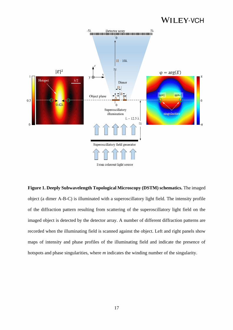
The results of our numerical microscopy experiments are presented in Figure 2. They
demonstrate that the dimensions of the dimer and its position can be retrieved accurately.
Indeed, on Figure 2 the solid red and blue lines correspond to the median of the true values as
a function of the retrieved value, whereas the black solid line is the bisector of the first quadrant
(y=x) representing perfect agreement between true and retrieved values. A departure of the
median from the bisector represents a systematic bias in the retrieval process. When the position
of the dimer is known, we obtain remarkably accurate retrieval of all dimensions both for plane
wave (red lines) and topological superoscillatory illumination (blue lines), with the systematic
bias of ~λ/100 or smaller. Here, superoscillatory illumination gives similar results to plane wave
illumination for the size of dimer’s element A, but provides over a factor of x2 smaller
systematic bias for dimer gap B. When the dimer position is a priori unknown, the systematic
bias increases but remains sub-λ/100 with superoscillatory illumination still giving better results
for retrieval of dimer gap B and position D than plane wave illumination. See Supporting
Information for more details.
7
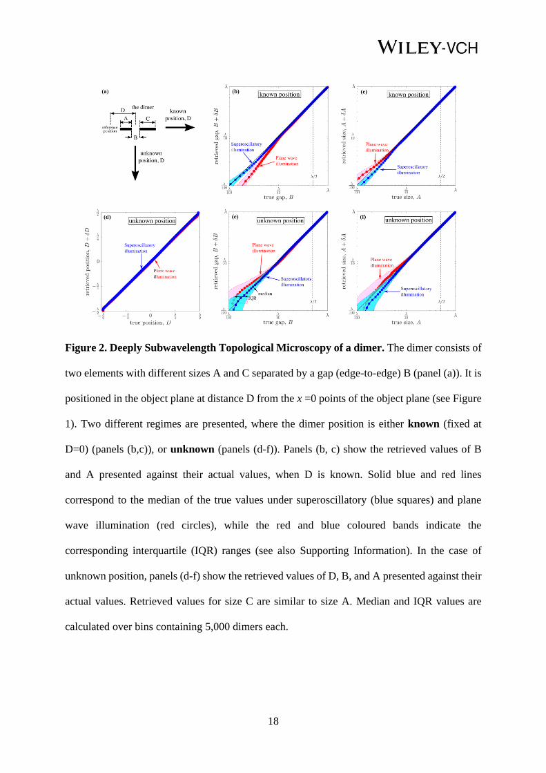
The Deeply Subwavelength Topological Microscopy reported here retrieves the dimer’s
geometric dimensions probabilistically. Thus, we define as the resolution of DSTM the spread
of retrieved values around the real value as quantified by the interquartile range (IQR), which
indicates the interval within which 50% of the retrieved values are found (see Figure 3). Since
IQR does not vary significantly with the dimensions of the dimer, we use its mean value as the
method’s resolution. Remarkably, in the case of known position and superoscillatory
illumination, the resolution of the imaging process exceeds λ/200 for all dimer dimensions.
When the position of the dimer is not known, the resolution decreases to ~λ/80 for
superoscillatory illumination. In both cases, superoscillatory illumination provides a resolution
enhancement of >50% over plane wave illumination (see Supporting Information).
The imaging results presented in Figure 3 were obtained by using the field amplitude of
the diffracted pattern resolved with 16-bit precision corresponding to a dynamic range of 96
dB. Here the dynamic range is defined as 10·log10(Imax/Imin), where Imin and Imax are the
minimum and maximum intensity levels that can be recorded. Although such dynamic range is
achievable with high-quality photodetectors, the resolution of the method is weakly dependent
on the detector’s dynamic range. To illustrate this, the detector’s dynamic range was
deliberately reduced by rounding readings to lower values (Figure 3f). Nevertheless, resolution
at the λ/100 scale is achieved even for 40 dB dynamic range, whereas typical photodiode values
are well above the 60 dB level.
Apart from the dynamic range of the detectors that we discussed above, resolution will
also be constrained by noise at the detector. However, our results (see Figure S3 in Supporting
Information) indicate a remarkable resilience of the method: even in the case of 5% random
noise (a very high value for high quality electro-optical systems), a dimer can be imaged at a
resolution of ~λ/71 for the element size, ~λ/77 for the gap, and ~λ/92 for the position. Finally,
an additional restriction is imposed by stability and the precision of optomechanical
components, which will be at the Angstrom scale (as is the case for atomic force microscopy).
8
In practical terms, the main challenge in the experimental implementation of DSTM
would be in creating reliable and trustworthy training sets for deep learning. Such datasets can
be either virtual or physical. The computer generated training dataset of imaged objects and
their scattering patterns can be rapidly and accurately generated by computing scattering
profiles on a random set of virtual training objects. Here the main challenge is to make the
computer model congruent with the physical realization of the microscope to allow adequate
imaging of the real object. Alternatively, a physical dataset can be created by nanofabrication
of a number of real scattering elements by electron beam lithography or focused ion beam
milling followed by recording of their real scattering patterns in the physical imaging
microscope. Generating a physical set is labor-intensive, but such a set will be naturally
congruent with the imaging microscope. The choice of the training dataset (physical or virtual)
will be informed by the desired resolution and complexity of the microscope optical tract. In
fact, we expect that the required dataset size will scale with the complexity and dimensionality
of the imaging target and the a priori available information. Indeed, objects of higher
complexity or dimensionality (e.g. from 1D to 2D or 3D) will be described by a larger number
of geometric dimensions and thus, we argue that increasingly larger training datasets will be
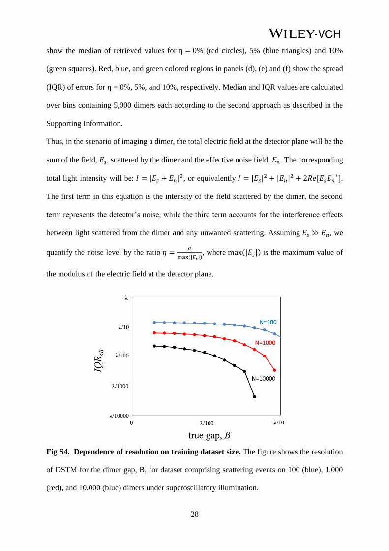
required. Here, we shall note that the size of the training set dramatically depends on the
required resolution. For instance, if in dimer microscopy the required resolution is only λ/10, a
training set involving only ~100 objects is needed, while microscopy with resolution exceeding
λ/200 may require training datasets comprising scattering events on tens of thousands objects
(see Supporting Information, Figure S4). Such large physical training datasets can be
manufactured on a single wafer by standard lithography methods. Moreover, it shall be noted
that depending on the size of the training dataset and the complexity of the imaging target
training of the network may take considerable time (one hour in a multi-GPU workstation in
our demo numerical experiments described above). However,once trained, image
reconstruction is possible with video frame rates.
9
We demonstrate the practicality of using physical datasets in DSTM by proof-of
principle experiments on imaging of dimer slits fabricated in an opaque metallic film by focused
ion beam milling. Each dimer comprises a pair of nanometer scale slits of unknown width in
the range 0.26λ-1.10λ and spacing between them in the range 0.17λ-0.94λ (see Supporting
information for experimental details).
For the experiment we use the framework of a conventional dual microscope equipped
with a sample piezo nano-positioning stage with 100 nm resolution. The dimer is placed on the
object plane of the imaging apparatus and illuminated with coherent laser light at the
wavelength λ=488nm. Light diffracted on the dimer is then imaged at a distance of h=2λ from
the image plane by a high-numerical lens (NA=0.95) and a 2.1-megapixel sCMOS array. Since
the diffracted field reaching the detector array is formed by free-space propagating waves, it
can be imaged at any magnification without loss of resolution by adjusting the magnification
level necessary to ensure that the detector pixels are smaller than the required resolution. The
imaging system of our apparatus had magnification of 400 corresponding to the pixel size of
12.6 nm on the image plane.
We used two types of illumination created by a computer-controlled wavefront
synthesizer system based on spatial light modulators.[24] In the DSTM modality, we used
topologically structured light illumination consisting of a superoscillatory sub-diffraction
hotspot surrounded by a halo of concentric rings. Results obtained with topologically structured
illumination were compared to Gaussian profile illumination with a focus larger than the dimer.
In the DSTM regime, the measurements were performed at 21 different positions of the
superoscillatory hotspot on the dimer, by gradually shifting the hotspot with steps of λ/4.9
perpendicular to the slit direction using the piezo nano-positioning stage.
The full experimental set consisted of 144 dimers, of which 115 dimers were used for
neural network training, 14 dimers for validation, and 15 dimers for our test imaging
10
experiments. Upon fabrication all dimers were measured to nanometer precision with a
scanning electron microscope. The diffraction patterns from the set of 115 dimers were recorded
in the imaging apparatus and together with their dimensions as measured by a scanning electron
microscope (SEM) formed the neural network training set. According to our modelling, even
such a small training set of only 115 dimers is sufficient to achieve resolution beyond λ/10.
Upon completion of the training the apparatus was ready for imaging dimers of
unknown size. Owing to the small size of the dataset and the stochastic character of the network
training process, DSTM retrieves dimer dimensions probabilistically. Thus, here we repeat the
training process for 500 different realizations of the neural network and present the
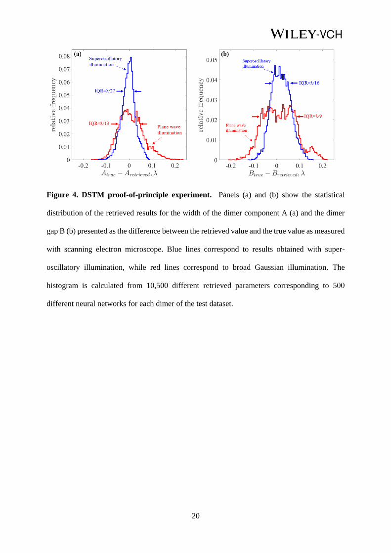
corresponding average values in Figure 4 a-b. We observed that:
1. When imaging a dimer in real experiments, its gap B and widths of the slits A and C are
retrieved with sub-diffraction resolution;
2. Accuracy (resolution) of retrieving size of the gap and width of the slits measured as
dispersion of results from different realizations of the neural network is higher for
topologically structured illumination than for Gaussian profile illumination;
3. Even a small training set of 115 dimers has been sufficient to achieve deeply
subwavelength resolution of λ/16 for the gap and λ/27 for the slit width (as quantified
by the by the interquartile range of the distribution) using topologically structured light
illumination. At the same time Gaussian illumination only returned resolution of λ/9 for
the gap and λ/13 for the slits.
We argue that the observed factor of approximately x2 improvement of the resolution with
topologically structured light illumination in comparison with Gaussian illumination reported
in this proof-of-principle experiment can be improved much further by increasing the number
of different positions of the superoscillatory hotspot on the object (the step size in the current
experiment is λ/4.9 =100 nm). The fine scanning will take full advantage of strong variations
11
of the scattered field when the structural features of the object overlap with that of the
illuminating field (see Figure 5 and discussion below). This would require a more precise
sample positioning system and improved mechanical stability of the imaging apparatus at the
level of AFM/STM instruments. Nevertheless, our results unambiguously demonstrate the
resolution advantages that topologically structured illumination delivers.
3. Discussion
The numerical DSTM experiments performed with large training sets and real proof-of-
principle experiments conducted with a small training set confirmed that artificial intelligence
enabled retrieval of the imaging target dimensions from the intensity patterns of the scattered
field delivers deeply subwavelength resolution. The deeply subwavelength level of resolution
reported here significantly exceeds the Abbe “diffraction limit” of resolution (~λ/2). We have
also observed, both in numerical and real experiment that using topologically structured
illumination increases the resolution of microscopy. We argue that several factors contribute
to this improvement:
1. Recording of multiple scattering patterns during the training process and
imaging provides much more information on the imaged object for the retrieval process than
what is available in the lens-generated single image for which the Abbe limit has been derived;
2. The deep learning process involving a neural network trained on a large dataset
creates a powerful and accurate deconvolution mechanism without using explicit information
on the phase of the detected signals;
3. Sparsity of the object and prior knowledge about the object (dimer of unknown
size and location) help the retrieval process, similarly to how sparsity helps ‘blind’ compressed
sensing techniques;[16]
12
4. Topological illumination ensures much higher sensitivity of the pattern of
scattered light to small features of the imaged object than conventional illumination.
The last argument requires a more detailed comment. It shall be noted that
superoscillatory fields contain zones of rapid phase gradient and high local wave vectors
leading to high spatial resolution through Fourier connection between spatial and reciprocal
space. Although this fact is reassuring, its full implication is difficult to analyze in the context
of the multiple exposures and the neural network deconvolution used in the DSTM technique.
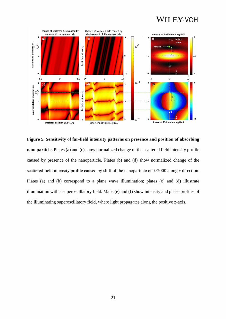
Instead, in Figure 5 we illustrate the sensitivity of the scattered field pattern on placing a small
absorbing nanoparticle in the illuminating topological field. The nanoparticle, only λ/1000 in
size, is positioned on the object plane at coordinate x0 (see Figure 1 and Figure 5e-f) and
illuminated with coherent light of wavelength λ. The intensity of the scattered light is detected
at a distance z = 10λ from the nanoparticle at points with coordinates (x, z =10λ). Maps (a) and
(c) in Figure 5 illustrate sensitivity of scattering to the presence of the particle in the illuminating
field for plane wave and superoscillatory illumination, respectively. They show the normalized
change of the intensity of scattered light (colormap, logarithmic scale) as a function of the
particle position x0 on the object plane and the detector’s coordinate x. Maps (b) and (d)
illustrate sensitivity of scattering to small displacements of the particle. They show the
normalized change of the scattered field intensity (colormap, logarithmic scale) on displacing
the particle with step of λ/2000 along the object plane with the particle initially located at x0.
From Figure 5, it follows that scattering of the superoscillatory field is two to three orders of
magnitude more sensitive than in the case of plane wave illumination to the presence and
repositioning of the nanoparticle, which we attribute to the presence of high intensity and phase
gradients in the superoscillatory field. This stronger sensitivity of the superoscillatory field
explains the enhancement of resolution comparatively to plane wave illumination. In particular
(see Figure 5c), placing the particle anywhere apart from the very narrow subwavelength
singularity zone (black horizontally extended area indicated by green dotted line) results in a
13
strong change of intensity across the detector plane. Figure 5d shows that when the nanoparticle
is repositioned away from the singularity point in the object plane, a very narrow, deeply
subwavelength zone is created on the detector plane where no change of intensity is taking
place. These features can be used to accurately retrieve the particle position. We argue that
enhancement of resolution with topological light against plane wave illumination shall increase
with the number of positions at which the object is illuminated. Indeed, fine scanning of the
object in the topological field improves chances of overlap between the fine features of the
object and zones of rapid phase variation that are crucial for high resolution image
reconstruction.
The deeply subwavelength topological microscopy (DSTM) reported here shall be
compared with confocal microscopy that uses a superoscillatory subwavelength intensity
hotspot for object illumination.[24] The image is reconstructed point-by-point by scanning the
hotspot against the object while it is imaged by a conventional lens through a confocal
aperture.[25] In this case, the size of the superoscillatory hotspot determines the resolution of the
technique.[26] Although, in principle, the superoscillatory hotspot can be arbitrary small,
intensity in the hotspot rapidly drops with its size, and resolution better than λ/4 has never been
experimentally demonstrated. As we have shown here, the resolution of DSTM could be orders
of magnitude better than confocal microscopy with superoscillatory illumination.
4. Conclusions
In conclusion, we have introduced the new concept of Deeply Subwavelength Topological
Microscopy (DSTM), which employs artificial intelligence to retrieve, with deeply
subwavelength resolving power, dimensions of a physical object from its scattering pattern
upon topological illumination. Although so far the concept has been demonstrated both
computationally and in proof-of-principle experiments for one-dimensional imaging, we expect
it will be readily extended to two- and three-dimensional objects, as well as objects of random
14
shape, and could be very efficient in microscopy of a priori known shapes, such as found in
routine tasks of machine vision, smart manufacturing, particle counting for life sciences
application etc. The technique does not require labelling of the sample with luminescent
materials, nor intense laser illumination thus avoiding photodamage effects, is resilient to noise
and we expect that it can work in both transmission and reflection mode depending on the
imaging target. The technique could lead to far-reaching consequences across a number of
disciplines, such as biomedical sciences, materials science and nanotechnology.
Supporting Information
Supporting Information is available from the Wiley Online Library or from the author.
Acknowledgements
This work was supported by the Singapore Ministry of Education (Grant No. MOE2016-T3-1-
006), the Agency for Science, Technology and Research (A*STAR) Singapore (Grant No.
SERC A1685b0005), the Engineering and Physical Sciences Research Council UK (Grants No.
EP/N00762X/1 and No. EP/M0091221), and the European Research Council (Advanced grant
FLEET-786851). T.P. acknowledges the support of the Chinese Scholarship Council (CSC No.
201804910540). N.I.Z., V.S., N.P., and G.Y. are inventors on UK patent application
1908500.0. The authors declare no other competing interests. Following a period of embargo,
the data from this paper can be obtained from the University of Southampton ePrints research
repository: https://doi. org/10.5258/SOTON/XXXX.
Received: ((will be filled in by the editorial staff))
Revised: ((will be filled in by the editorial staff))
Published online: ((will be filled in by the editorial staff))
15
References
[1] G. H. Yuan, N. I. Zheludev, Science 2019, 364, 771.
[2] S. W. Hell, Science 2007, 316, 1153.
[3] E. Betzig et al., Science 2006, 313, 1642.
[4] M. J. Rust, M. Bates, X. W. Zhuang, Nat. Methods 2006, 3, 793.
[5] T. Pu, J. Y. Ou, N. Papasimakis, N. I. Zheludev, Appl. Phys. Lett. 2020, 116, 131105.
[6] https://en.wikipedia.org/wiki/Imaging.
[7] https://en.wikipedia.org/wiki/Microscopy
[8] G. Yuan, E. T. F. Rogers, N. I. Zheludev, Light: Sci. & Appl. 2019, 8, 2.
[9] M. V. Berry, M. R. Dennis. Proc. R. Soc. A 457, 2251-2263 (2001).
[10] M. V. Berry, S. Popescu, J. Phys. A 2006, 39, 6965.
[11] F. M. Huang, N. I. Zheludev, Nano Lett. 2009, 9, 1249.
[12] A. J. Devaney, Mathematical foundations of imaging, tomography and wavefield
inversion, Cambridge University Press, New York, USA 2012.
[13] M. Paúr, B. Stoklasa, Z. Hradil, L. L. Sánchez-Soto, J. Rehacek, Optica 2016, 3, 1144.
[14] P. Thibault, V. Elser, Ann. Rev. Condens. Matter Phys. 2010, 1, 237-255 (2010).
[15] H. Yu, R. Lu, S. Han, H. Xie, G. Du, T. Xiao, D. Zhu, Phys. Rev. Lett. 2016, 117, 113901.
[16] S. Gleichman, Y. C. Eldar, IEEE Trans. Inform. Theory 2011, 57, 6958.
[17] S. Gazit, A. Szameit, Y. C. Eldar, M. Segev, Opt. Express 2009, 17, 23920.
[18] K. Nasrollahi, T. B. Moeslund. Mach. Vision Appl. 2014, 25, 1423.
[19] C. Dong, C. C. Loy, K. M. He, X. O. Tang, IEEE Trans. Patern Anal. Mach. Intell. 2016, 38,
295.
[20] H. Wang, Y. Rivenson, Z. Wei, T. Gao, H. Gunaydin, L. Bentolila, C. Kural, A. Ozcan,
Nature Methods 2019, 16, 103.
[21] C. Belthangady, L. A. Royer, Nature Methods 2019, 1215-1225 (2019).
[22] A. Krizhevsky, I. Sutskever, G. E. Hinton, Adv. Neural Inf. Process. Syst. 2012, 25, 1106.

16
[23] D. Kingma, J. Ba, arXiv:1412.6980 2014.
[24] E. T. F. Rogers, S. Quraishe, K. S. Rogers, T. A. Newman, P. J. S. Smith and N. I. Zheludev.
APL Photonics 2020, 5, 066107.
[25] E. T. F. Rogers, J. Lindberg, T. Roy, S. Savo, J. E. Chad, M. R. Dennis, N. I. Zheludev, Nat.
Mater. 2012, 11, 432.
[26] G. H. Yuan, K. S. Rogers, E. T. F. Rogers, N. I. Zheludev, Phys. Rev. Applied 2019, 11,
064016.
17
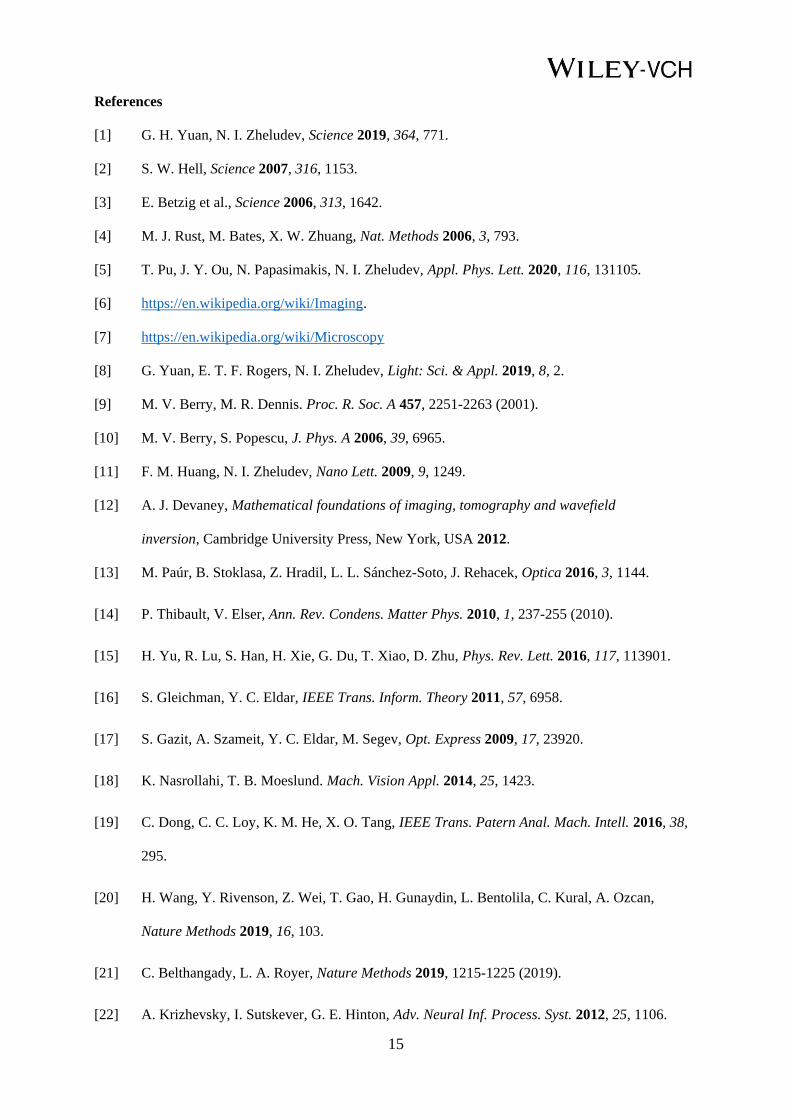
Figure 1. Deeply Subwavelength Topological Microscopy (DSTM) schematics. The imaged
object (a dimer A-B-C) is illuminated with a superoscillatory light field. The intensity profile
of the diffraction pattern resulting from scattering of the superoscillatory light field on the
imaged object is detected by the detector array. A number of different diffraction patterns are
recorded when the illuminating field is scanned against the object. Left and right panels show
maps of intensity and phase profiles of the illuminating field and indicate the presence of
hotspots and phase singularities, where m indicates the winding number of the singularity.
18
Figure 2. Deeply Subwavelength Topological Microscopy of a dimer. The dimer consists of
two elements with different sizes A and C separated by a gap (edge-to-edge) B (panel (a)). It is
positioned in the object plane at distance D from the x =0 points of the object plane (see Figure
1). Two different regimes are presented, where the dimer position is either known (fixed at
D=0) (panels (b,c)), or unknown (panels (d-f)). Panels (b, c) show the retrieved values of B
and A presented against their actual values, when D is known. Solid blue and red lines
correspond to the median of the true values under superoscillatory (blue squares) and plane
wave illumination (red circles), while the red and blue coloured bands indicate the
corresponding interquartile (IQR) ranges (see also Supporting Information). In the case of
unknown position, panels (d-f) show the retrieved values of D, B, and A presented against their
actual values. Retrieved values for size C are similar to size A. Median and IQR values are
calculated over bins containing 5,000 dimers each.
19
Figure 3. Resolution of the Deeply Subwavelength Topological Microscopy. IQRs of
measured values of the dimer dimensions, gap, B (a,d), element size, A (b,e), and position, D
(c), during numerical imaging experiments with unknown (a-c) and known (d-e) dimer position.
Red and blue colored regions correspond to plane wave and superoscillatory illumination,
respectively, while red and blue solid lines mark the first and the third quartiles of the
corresponding error distributions. The horizontal dotted lines indicate the average value of the
IQRs over the range of the true values of the respective dimension. The vertical dotted lines in
panels (a) and (b) indicate the geometric dimension’s true value below which the network
returns predominantly negative, non-physical values. IQR values are calculated over bins
containing 5,000 dimers each. (f) Dependence of resolution (in dimer gap B) as a function of
the dynamic range of the photodetector.
20
Figure 4. DSTM proof-of-principle experiment. Panels (a) and (b) show the statistical
distribution of the retrieved results for the width of the dimer component A (a) and the dimer
gap B (b) presented as the difference between the retrieved value and the true value as measured
with scanning electron microscope. Blue lines correspond to results obtained with super-
oscillatory illumination, while red lines correspond to broad Gaussian illumination. The
histogram is calculated from 10,500 different retrieved parameters corresponding to 500
different neural networks for each dimer of the test dataset.
21
Figure 5. Sensitivity of far-field intensity patterns on presence and position of absorbing
nanoparticle. Plates (a) and (c) show normalized change of the scattered field intensity profile
caused by presence of the nanoparticle. Plates (b) and (d) show normalized change of the
scattered field intensity profile caused by shift of the nanoparticle on λ/2000 along x direction.
Plates (a) and (b) correspond to a plane wave illumination; plates (c) and (d) illustrate
illumination with a superoscillatory field. Maps (e) and (f) show intensity and phase profiles of
the illuminating superoscillatory field, where light propagates along the positive z-axis.
22
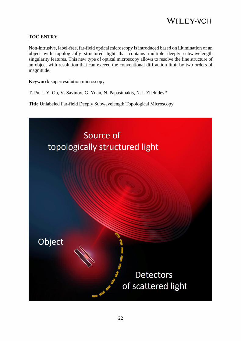
TOC ENTRY
Non-intrusive, label-free, far-field optical microscopy is introduced based on illumination of an
object with topologically structured light that contains multiple deeply subwavelength
singularity features. This new type of optical microscopy allows to resolve the fine structure of
an object with resolution that can exceed the conventional diffraction limit by two orders of
magnitude.
Keyword: superresolution microscopy
T. Pu, J. Y. Ou, V. Savinov, G. Yuan, N. Papasimakis, N. I. Zheludev*
Title Unlabeled Far-field Deeply Subwavelength Topological Microscopy
23
Supporting Information
Unlabeled Far-field Deeply Subwavelength Topological Microscopy
Tanchao Pu, Jun-Yu Ou, Vassili Savinov, Guanghui Yuan, Nikitas Papasimakis, Nikolay I.
Zheludev*
S1. Numerical methods
In the numerical imaging experiments, the superoscillatory field generator is scanned across the
object by steadily moving the superoscillatory hotspot, at intervals of λ/5, from the -λ position
to the +λ position in the object plane. For each position of the hotspot the detector records a
diffraction pattern. The full set of diffraction patterns is analyzed by a Convolutional Neural
Network[1] to retrieve information about the object. The network contains three convolution
layers with 32-5×5, 32-3×3, 64-3×3 and 32-1×1 kernels, correspondingly, and three fully
connected layers with 128, 32, 4 neurons, respectively. The first three convolution layers are
separately followed by a pooling layer with 1×4, 1×8, 1×4 kernels with Rectified Linear Unit
activation function. The network was trained with the Adam stochastic optimization method[2]
and mean absolute error loss function, aimed at improving the retrieval of the dimer geometrical
dimensions, i.e. constants A, B, C and D. The training dataset contained 20,000 samples and
was generated by creating dimers of random sizes and placing them on the object plane with
the dimer centre coordinate D randomly chosen in the interval from –λ/2 to λ/2 (in the case of
unknown dimer position). The widths of the dimer components (A and C) and the gap between
them (B) were independently and randomly chosen between 0.002λ and λ. The diffraction
pattern on the detector array was then calculated by the Fourier propagation method[3] for the
transverse component of the electric field.
In the real-life imaging experiments with superoscillatory illumination, the recorded
scattering patterns were processed by a convolutional neural network consisting of 4
24
convolutional layers, 2 dense layers activated by a ReLU function, and an output layer with a
sigmoid activation function. The first three convolutional layers contained 64, 112, and 112
3*3-filters, while the fourth convolutional layer contained 32 1*1-filters. There were 64, 16 and
3 neurons in the dense layers and output layer, respectively. In the case of plane wave
illumination, the neural network comprised 3 dense layers with 128, 512, 256 neurons activated
by ReLU function and an output layer with 3 neurons activated by a sigmoid function.
The training time in the case of the numerical experiments was ~1h using a multi-GPU
server (4 x GTX1080), while for the experimental results training took ~2 min in a standard
desktop PC.
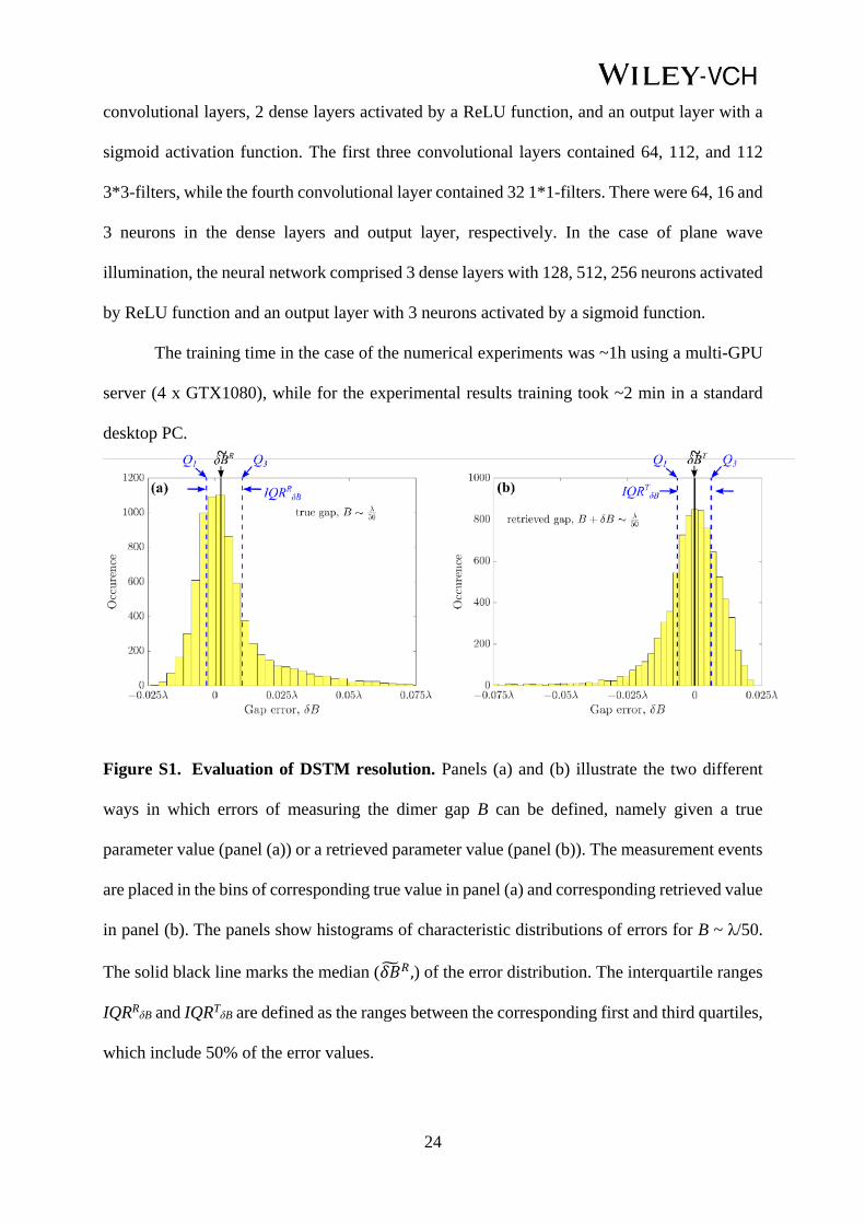
Figure S1. Evaluation of DSTM resolution. Panels (a) and (b) illustrate the two different
ways in which errors of measuring the dimer gap B can be defined, namely given a true
parameter value (panel (a)) or a retrieved parameter value (panel (b)). The measurement events
are placed in the bins of corresponding true value in panel (a) and corresponding retrieved value
in panel (b). The panels show histograms of characteristic distributions of errors for B ~ λ/50.
The solid black line marks the median (𝛿�̃�𝑅 ,) of the error distribution. The interquartile ranges
IQRRδB and IQRT
δB are defined as the ranges between the corresponding first and third quartiles,
which include 50% of the error values.
25
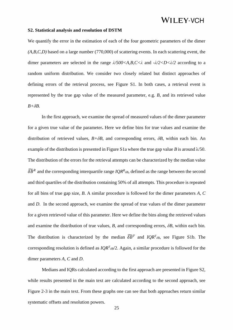
S2. Statistical analysis and resolution of DSTM
We quantify the error in the estimation of each of the four geometric parameters of the dimer
(A,B,C,D) based on a large number (770,000) of scattering events. In each scattering event, the
dimer parameters are selected in the range λ/500<A,B,C<λ and -λ/2<D<λ/2 according to a
random uniform distribution. We consider two closely related but distinct approaches of
defining errors of the retrieval process, see Figure S1. In both cases, a retrieval event is
represented by the true gap value of the measured parameter, e.g. B, and its retrieved value
B+δB.
In the first approach, we examine the spread of measured values of the dimer parameter
for a given true value of the parameter. Here we define bins for true values and examine the
distribution of retrieved values, B+δB, and corresponding errors, δB, within each bin. An
example of the distribution is presented in Figure S1a where the true gap value B is around λ/50.
The distribution of the errors for the retrieval attempts can be characterized by the median value
𝛿�̃�𝑅 and the corresponding interquartile range IQRRδB, defined as the range between the second
and third quartiles of the distribution containing 50% of all attempts. This procedure is repeated
for all bins of true gap size, B. A similar procedure is followed for the dimer parameters A, C
and D. In the second approach, we examine the spread of true values of the dimer parameter
for a given retrieved value of this parameter. Here we define the bins along the retrieved values
and examine the distribution of true values, B, and corresponding errors, δB, within each bin.
The distribution is characterized by the median 𝛿�̃�𝑇 and IQRTδB, see Figure S1b. The
corresponding resolution is defined as IQRTδB/2. Again, a similar procedure is followed for the
dimer parameters A, C and D.
Medians and IQRs calculated according to the first approach are presented in Figure S2,
while results presented in the main text are calculated according to the second approach, see
Figure 2-3 in the main text. From these graphs one can see that both approaches return similar
systematic offsets and resolution powers.
26
Figure S2. Imaging errors for dimer imaging. The retrieved values of the dimer parameter
for a given true value of the parameters are presented. (a) Schematic of the dimer and its
geometric parameters. Panels (b) and (c) show measurement results if location D of the dimer
is known. Solid blue and red lines correspond to the median of the retrieved values under
superoscillatory (blue squares) and plane wave illumination (red circles), while the red and blue
colored bands indicate the corresponding interquartile (IQR) ranges. In the case of unknown
position of the dimer, panels (d) and (f) show the retrieved values of A, B and D against their
actual values. Median and IQR values are calculated over bins containing 5,000 dimers each
according to the first approach as described in the Supporting Information.
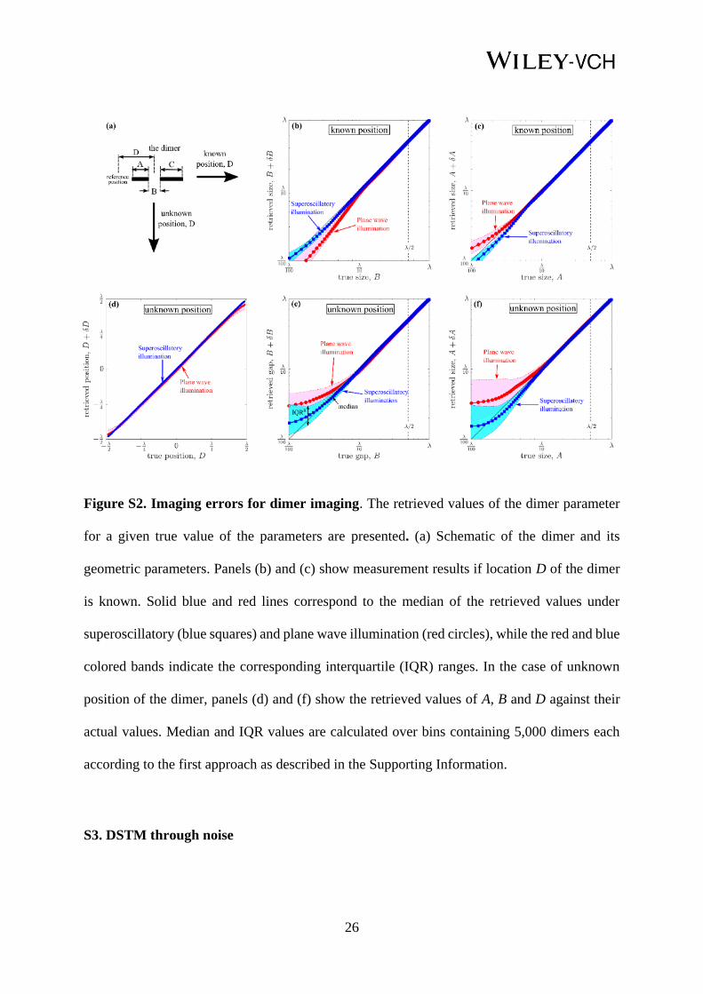
S3. DSTM through noise
27
Here we examine sensitivity of the DSTM method to noise. In a practical implementation of
the method, noise can arise either as detection noise or due to unwanted scattering and
interference effects. We model both of these effects by introducing an effective “noise field”,
𝐸𝑛, at the detector plane, which takes values according to a zero mean Gaussian distribution
with standard deviation σ.
Fig S3. Resilience of DSTM to noise. The figure shows the effects of different levels of noise
η on the retrieved dimer element size A (a,b), gap B (b,e), and position D (c,f). Panels (a-c)
28
show the median of retrieved values for η = 0% (red circles), 5% (blue triangles) and 10%
(green squares). Red, blue, and green colored regions in panels (d), (e) and (f) show the spread
(IQR) of errors for η = 0%, 5%, and 10%, respectively. Median and IQR values are calculated
over bins containing 5,000 dimers each according to the second approach as described in the
Supporting Information.
Thus, in the scenario of imaging a dimer, the total electric field at the detector plane will be the
sum of the field, 𝐸𝑠, scattered by the dimer and the effective noise field, 𝐸𝑛. The corresponding
total light intensity will be: 𝐼 = |𝐸𝑠 + 𝐸𝑛|2, or equivalently 𝐼 = |𝐸𝑠|
2 + |𝐸𝑛|2 + 2𝑅𝑒[𝐸𝑠𝐸𝑛
∗].
The first term in this equation is the intensity of the field scattered by the dimer, the second
term represents the detector’s noise, while the third term accounts for the interference effects
between light scattered from the dimer and any unwanted scattering. Assuming 𝐸𝑠 ≫ 𝐸𝑛, we
quantify the noise level by the ratio 𝜂 =𝜎
max(|𝐸𝑠|), where max(|𝐸𝑠|) is the maximum value of
the modulus of the electric field at the detector plane.
Fig S4. Dependence of resolution on training dataset size. The figure shows the resolution
of DSTM for the dimer gap, B, for dataset comprising scattering events on 100 (blue), 1,000
(red), and 10,000 (blue) dimers under superoscillatory illumination.
29
Figure S3 shows the effect of noise on the retrieval of the dimer geometrical parameters.
The noise results in the increase of divergence (bias) of the median lines (Figure S3a&b) from
the line of perfect imaging (black line in Figure S3). In the case of 5% noise, substantial
divergence occurs for A<λ/77 and B<λ/65, while for noise levels of 10%, the median diverges
for A<λ/45 and B<λ/60.
The effects of noise on resolving power are presented in Figure S3d-f. Here, increasing
the noise level leads to gradual decrease of resolution. However, for all measured parameters
resolution at 5% and 10% noise level remains at deeply subwavelength level, i.e. better than
~λ/70 and ~λ/55 correspondingly. This illustrates a remarkable resilience of the deconvolution
process considering that we account for the interference phase related effects in the noise
without providing any phase information to the network.
Table S1. Resolution under superoscillatory and plane wave illumination. The values in
square brackets (for unknown position and under superoscillatory illumination) correspond to
the resolution in the presence of 5% noise.
Superoscillatory illumination Plane wave illumination
Unknown
position Known position Unknown position Known position
Resolution in dimer
element size, A 0.0133λ (λ/75)
[0.0142 (λ/71)] 0.0045λ (λ/222) 0.0214λ (λ/47) 0.0064λ (λ/156)
Resolution in dimer
gap, B 0.0122λ (λ/82)
[0.0130 (λ/77)] 0.0042λ (λ/238) 0.0192λ (λ/52) 0.0061λ (λ/164)
Resolution in position,
D 0.0111λ (λ/90)
[0.0108 (λ/92)] 0.0297λ (λ/34)
S4. Experimental setup for DSTM
The experimental demonstration of DSTM was carried out in a dual microscope with a custom
built computer-controlled wavefront synthesizer system based on spatial light modulators
(Meadowlark P512) and coherent laser source at wavelength λ=488nm (Newport Excelsior-
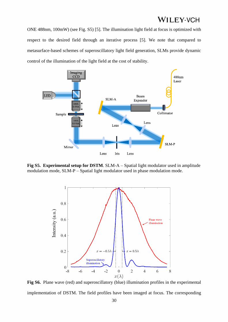
30
ONE 488nm, 100mW) (see Fig. S5) [5]. The illumination light field at focus is optimized with
respect to the desired field through an iterative process [5]. We note that compared to
metasurface-based schemes of superoscillatory light field generation, SLMs provide dynamic
control of the illumination of the light field at the cost of stability.
Fig S5. Experimental setup for DSTM. SLM-A – Spatial light modulator used in amplitude
modulation mode, SLM-P – Spatial light modulator used in phase modulation mode.
Fig S6. Plane wave (red) and superoscillatory (blue) illumination profiles in the experimental
implementation of DSTM. The field profiles have been imaged at focus. The corresponding
31
focal spot sizes are ~6.7λ and ~1.1λ for plane wave and superoscillatory illumination,
respectively. For both types of illuminations, the wavelength is λ=488 nm.
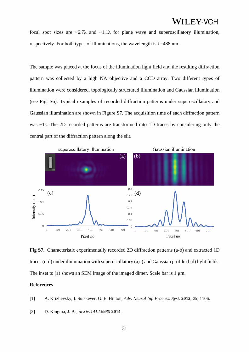
The sample was placed at the focus of the illumination light field and the resulting diffraction
pattern was collected by a high NA objective and a CCD array. Two different types of
illumination were considered, topologically structured illumination and Gaussian illumination
(see Fig. S6). Typical examples of recorded diffraction patterns under superoscillatory and
Gaussian illumination are shown in Figure S7. The acquisition time of each diffraction pattern
was ~1s. The 2D recorded patterns are transformed into 1D traces by considering only the
central part of the diffraction pattern along the slit.
Fig S7. Characteristic experimentally recorded 2D diffraction patterns (a-b) and extracted 1D
traces (c-d) under illumination with superoscillatory (a,c) and Gaussian profile (b,d) light fields.
The inset to (a) shows an SEM image of the imaged dimer. Scale bar is 1 μm.
References
[1] A. Krizhevsky, I. Sutskever, G. E. Hinton, Adv. Neural Inf. Process. Syst. 2012, 25, 1106.
[2] D. Kingma, J. Ba, arXiv:1412.6980 2014.

32
[3] J. W. Goodman, Introduction to Fourier optics, W.H. Freeman, Macmillan Learning, New
York, USA 2017.
[4] G. H. Yuan, K. S. Rogers, E. T. F. Rogers, N. I. Zheludev, Phys. Rev. Applied 2019, 11,
064016.
[5] E. T. F. Rogers, S. Quraishe, K. S. Rogers, T. A. Newman, P. J. S. Smith and N. I. Zheludev.
APL Photonics 2020, 5, 066107.