Embed Size (px)
Citation preview

MOSFET Transistors and Basic Circuits
Jennifer Hasler
CMOS Process Cross Sec:on
(n-‐well)
all p-n junction must be reversed bias
nFET pFET
CMOS Process = nFETs and pFETs are available
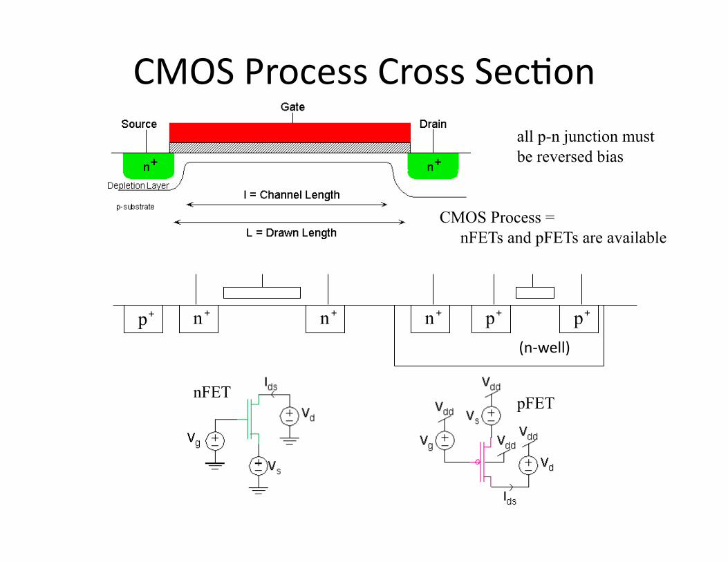
MOSFET Device Physics MOS Channel Behavior
MOS Capacitor Picture
• subthreshold operation = fundamental case
• Above VT: I > Ith, Ψ(x) in channel, Ψ(x) set by current level, terminal voltages
• Sub-VT: I < Ith Channel Potential (Ψ) is flat • Sub-VT operation simplifies this 2D problem to 2, 1D problems
ψ varies as κVG
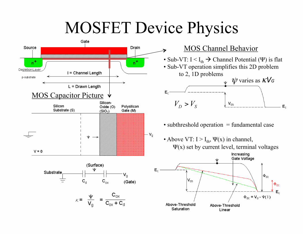
MOS Capacitor Behavior
Depletion: gate charge is terminated by charged ions in the depletion region
Inversion: further gate charge is terminated by carriers at the silicon--silicon-dioxide interface
V@ Flatband: no Q, bands are flat (occurs at V@)
Free Q parameter set by V@ ΔΨ = κ ΔVg
Ψ
Ψ
Increasing Gate Voltage: Flatband (Vfb) Depletion Inversion
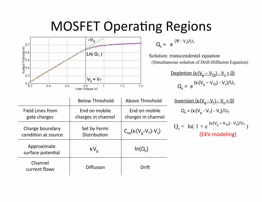
MOSFET Opera:ng Regions
End on mobile charges in channel
End on mobile charges in channel
Field Lines from gate charges
Below Threshold Above Threshold
Channel current flows Diffusion DriQ
Charge boundary condi:on at source
Set by Fermi Distribu:on
Cox(κ(Vg-‐VT)-‐Vs) Qs = ln( 1 + e ) (κ(Vg – VT0) -‐ Vs)/UT
Qs = e (Ψ -‐ Vs)/UT
Approximate surface poten:al
κVg ln(Qs)
(EKV modeling)
Deple:on (κ(Vg – VT0) -‐ Vs < 0)
Qs = e (κ(Vg – VT0) -‐ Vs)/UT
Inversion (κ(Vg -‐ VT) -‐ Vs > 0)
Qs = (κ(Vg -‐ VT) -‐ Vs)/UT
Solution: transcendental equation (Simultaneous solution of Drift-Diffusion Equation)
Sub VT Drain Current Deriva:on
€
nsource ∝ e−φ sc /UT
€
ndrain ∝ e−φ dc /UT
No recombination in channel
n(x) = Ax + B
R G dx
n d D dt dn
n - + Δ
= 2
2 0 0 0
n(x) = Ax + B
Is = Ith ( e - e ) (κ(Vg – VT0) -‐ Vs)/UT (κ(Vg – VT0) -‐ Vd)/UT
ψ varies as κVG
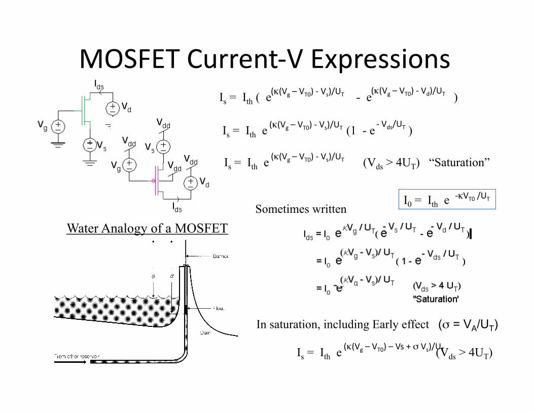
MOSFET Current-‐V Expressions Is = Ith ( e - e ) (κ(Vg – VT0) -‐ Vs)/UT (κ(Vg – VT0) -‐ Vd)/UT
Sometimes written I0 = Ith e -‐κVT0 /UT
Is = Ith e (1 - e ) (κ(Vg – VT0) -‐ Vs)/UT -‐ Vds/UT
Is = Ith e (Vds > 4UT) (κ(Vg – VT0) -‐ Vs)/UT “Saturation”
In saturation, including Early effect (σ = VA/UT)
Is = Ith e (Vds > 4UT) (κ(Vg – VT0) – Vs + σ Vs)/UT
Water Analogy of a MOSFET
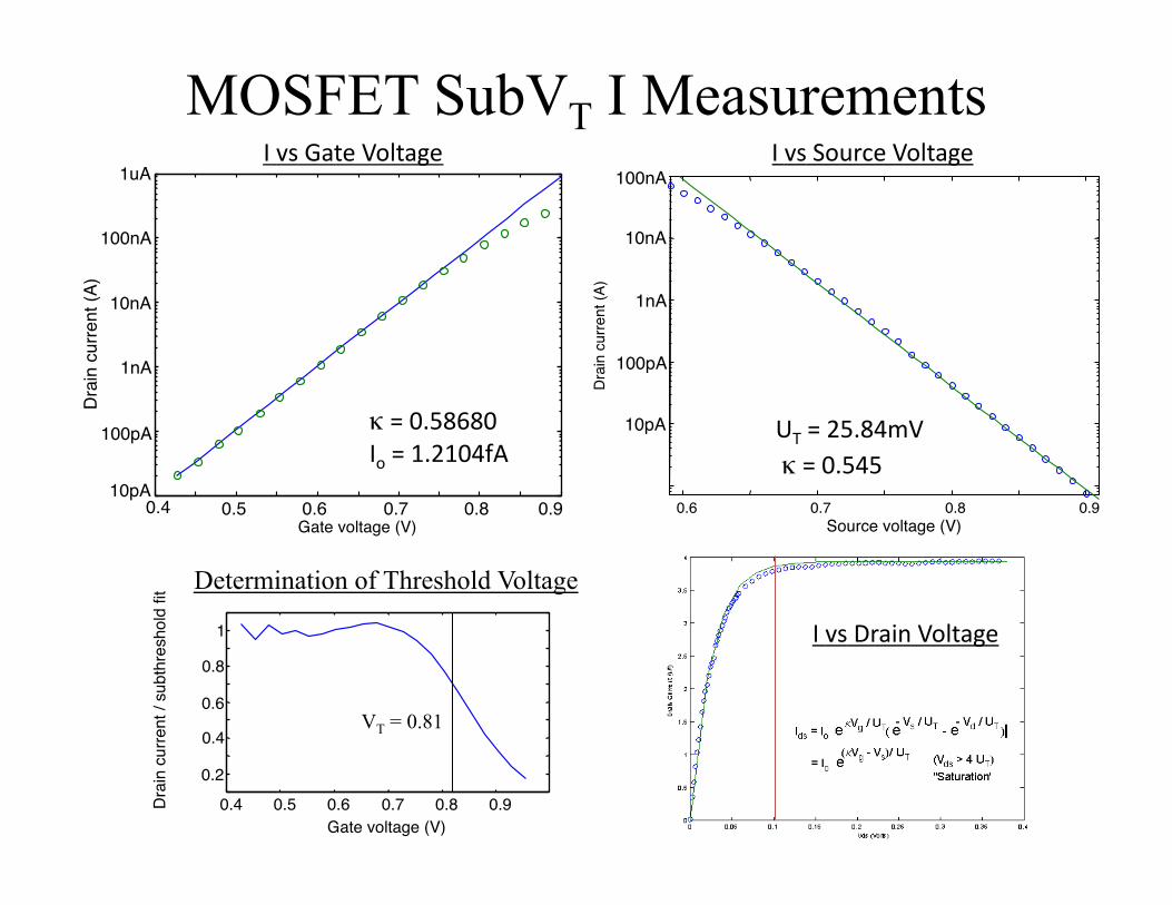
MOSFET SubVT I Measurements
0.4 0.5 0.6 0.7 0.8 0.9
100pA
1nA
Gate voltage (V)
Dra
in c
urre
nt (A
)
κ = 0.58680 Io = 1.2104fA
10nA
100nA
10pA
1uA I vs Gate Voltage
0.6 0.7 0.8 0.9 Source voltage (V)
Dra
in c
urre
nt (A
)
UT = 25.84mV κ = 0.545
100pA
1nA
10nA
100nA
10pA
I vs Source Voltage
Determination of Threshold Voltage
0.4 0.5 0.6 0.7 0.8 0.9 0.2 0.4 0.6 0.8
Gate voltage (V)
Dra
in c
urre
nt /
subt
hres
hold
fit
1
VT = 0.81
I vs Drain Voltage
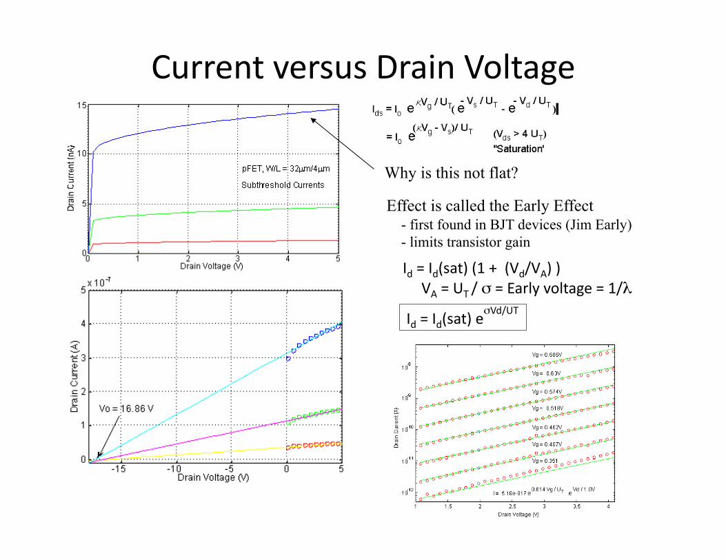
Current versus Drain Voltage
Why is this not flat?
Id = Id(sat) (1 + (Vd/VA) ) VA = UT / σ = Early voltage = 1/λ
Id = Id(sat) eσVd/UT
Effect is called the Early Effect - first found in BJT devices (Jim Early) - limits transistor gain
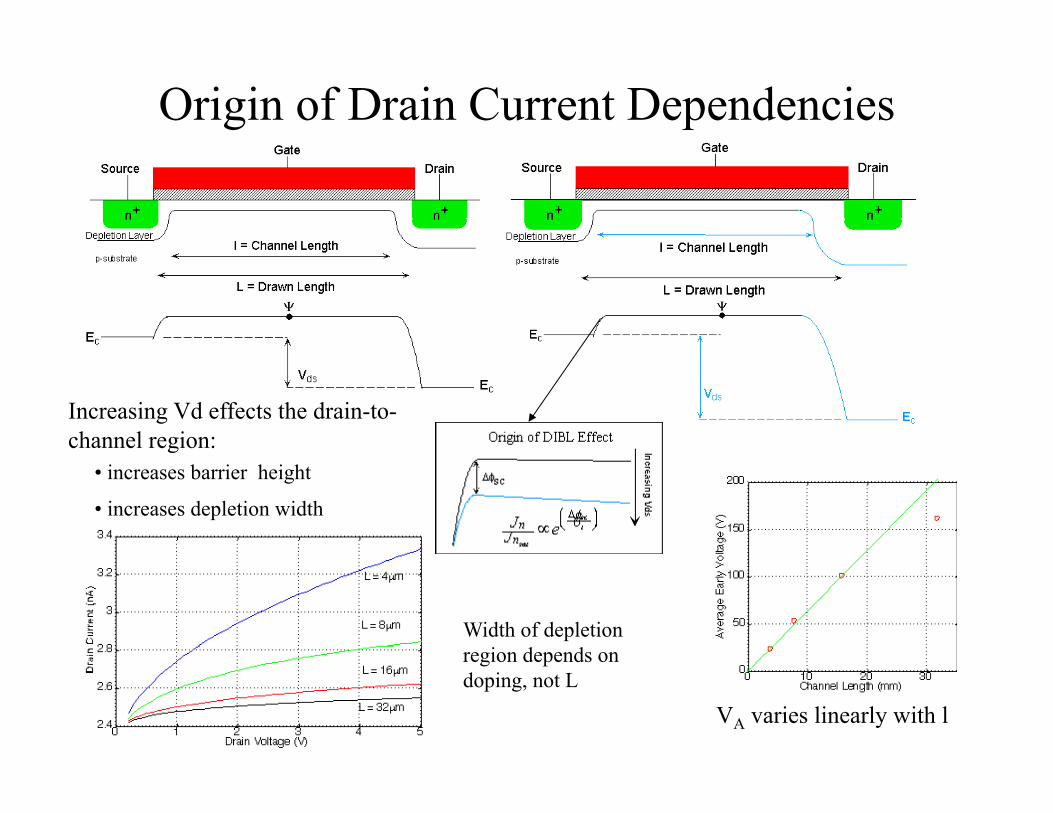
Origin of Drain Current Dependencies
Increasing Vd effects the drain-to-channel region:
• increases depletion width
• increases barrier height
VA varies linearly with l
Width of depletion region depends on doping, not L
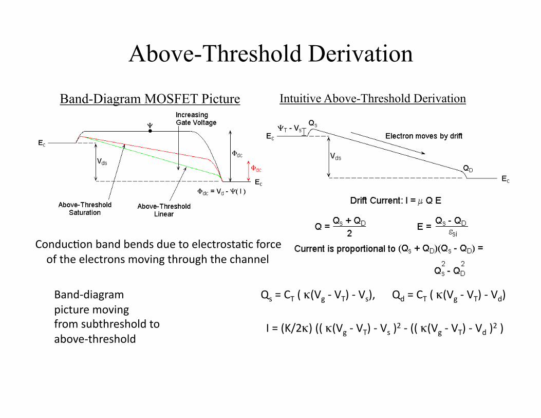
Above-Threshold Derivation
I = (K/2κ) (( κ(Vg -‐ VT) -‐ Vs )2 -‐ (( κ(Vg -‐ VT) -‐ Vd )2 )
Qs = CT ( κ(Vg -‐ VT) -‐ Vs), Qd = CT ( κ(Vg -‐ VT) -‐ Vd)
Intuitive Above-Threshold Derivation
Band-‐diagram picture moving from subthreshold to above-‐threshold
Conduc:on band bends due to electrosta:c force of the electrons moving through the channel
Band-Diagram MOSFET Picture
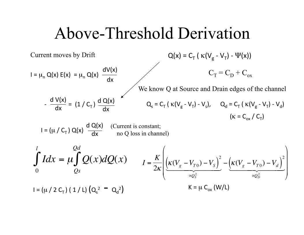
Above-Threshold Derivation Current moves by Drift
I = µn Q(x) E(x) = µn Q(x) dV(x)
dx
Q(x) = CT ( κ(Vg -‐ VT) -‐ Ψ(x))
CT = CD + Cox
Qs = CT ( κ(Vg -‐ VT) -‐ Vs), Qd = CT ( κ(Vg -‐ VT) -‐ Vd)
(κ = Cox / CT)
We know Q at Source and Drain edges of the channel
-‐ = (1 / CT ) d V(x) dx
d Q(x) dx
I = (µ / CT ) Q(x) d Q(x) dx
(Current is constant; no Q loss in channel)
€
I0
l
∫ dx = µ Q(x)Qs
Qd
∫ dQ(x)
I = (µ / 2 CT ) ( 1 / L) (Qs2 -‐ Qd
2) K = µ Cox (W/L)
€
I =K2κ
κ(Vg −VT 0) −VS( )2
∝QS2
− κ(Vg −VT 0) −Vd( )
2
∝QD2
⎛
⎝
⎜ ⎜ ⎜
⎞
⎠
⎟ ⎟ ⎟
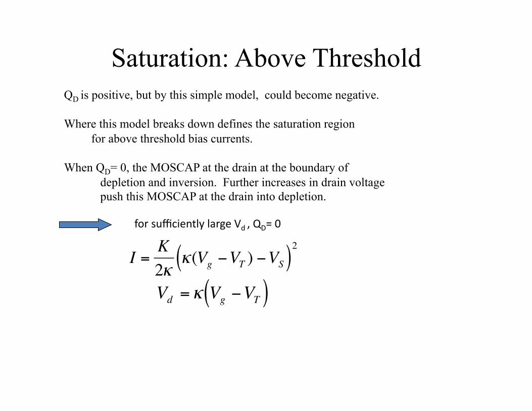
Saturation: Above Threshold QD is positive, but by this simple model, could become negative.
Where this model breaks down defines the saturation region for above threshold bias currents.
When QD= 0, the MOSCAP at the drain at the boundary of depletion and inversion. Further increases in drain voltage push this MOSCAP at the drain into depletion.
for sufficiently large Vd , QD= 0
€
I =K2κ
κ(Vg −VT ) −VS( )2
€
Vd =κ Vg −VT( )
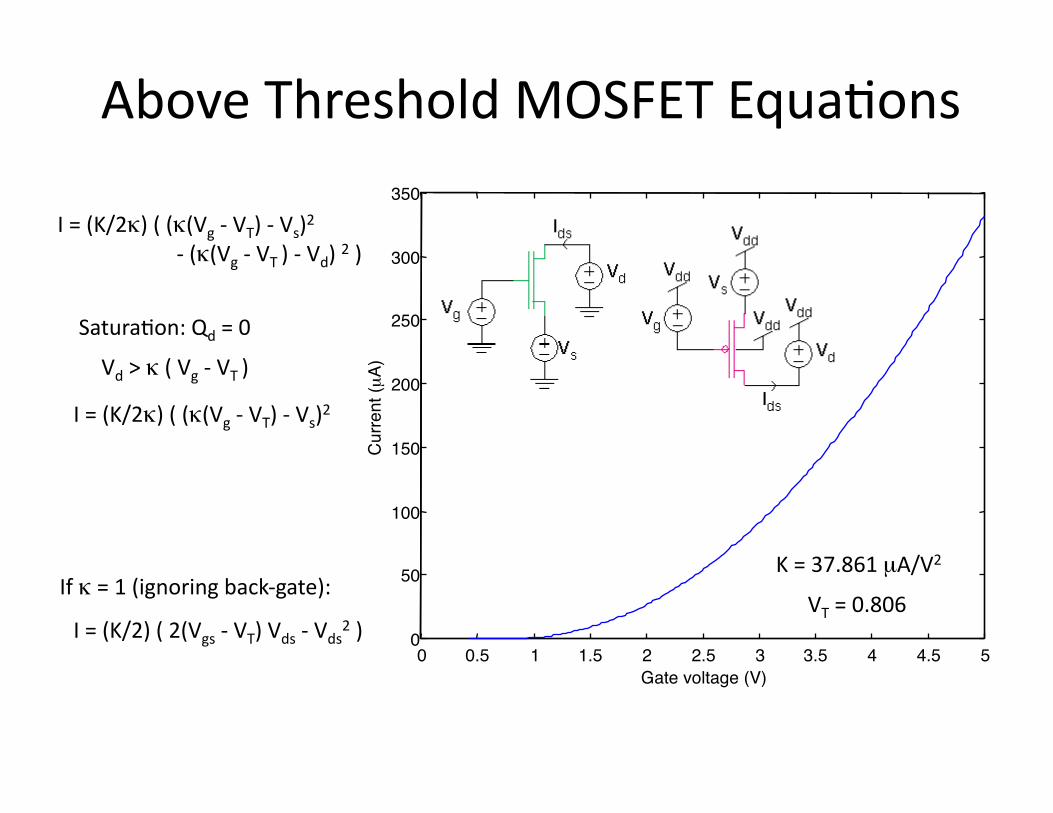
Above Threshold MOSFET Equa:ons
I = (K/2κ) ( (κ(Vg -‐ VT) -‐ Vs)2 -‐ (κ(Vg -‐ VT ) -‐ Vd) 2 )
Satura:on: Qd = 0
I = (K/2κ) ( (κ(Vg -‐ VT) -‐ Vs)2
If κ = 1 (ignoring back-‐gate):
I = (K/2) ( 2(Vgs -‐ VT) Vds -‐ Vds2 )
0 0.5 1 1.5 2 2.5 3 3.5 4 4.5 5 0
50
100
150
200
250
300
350
Gate voltage (V)
Cur
rent
(µA)
K = 37.861 µA/V2
VT = 0.806
Vd > κ ( Vg -‐ VT )
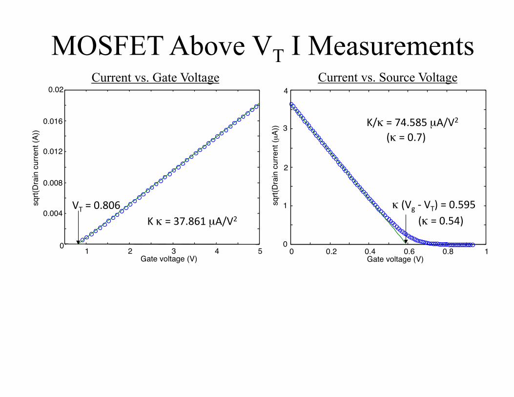
MOSFET Above VT I Measurements
1 2 3 4 50
0.004
0.008
0.012
0.016
0.02
Gate voltage (V)
sqrt(
Dra
in c
urre
nt (A
))
VT = 0.806 K κ = 37.861 µA/V2
0 0.2 0.4 0.6 0.8 10
1
2
3
4
Gate voltage (V) sq
rt(D
rain
cur
rent
(µA)
)
κ (Vg -‐ VT) = 0.595
K/κ = 74.585 µA/V2
(κ = 0.54)
(κ = 0.7)
Current vs. Gate Voltage Current vs. Source Voltage
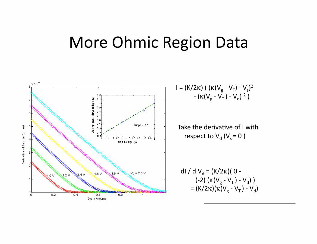
More Ohmic Region Data
I = (K/2κ) ( (κ(Vg -‐ VT) -‐ Vs)2 -‐ (κ(Vg -‐ VT ) -‐ Vd) 2 )
Take the deriva:ve of I with respect to Vd (Vs = 0 )
dI / d Vd = (K/2κ)( 0 -‐ (-‐2) (κ(Vg -‐ VT ) -‐ Vd) ) = (K/2κ)(κ(Vg -‐ VT ) -‐ Vd)
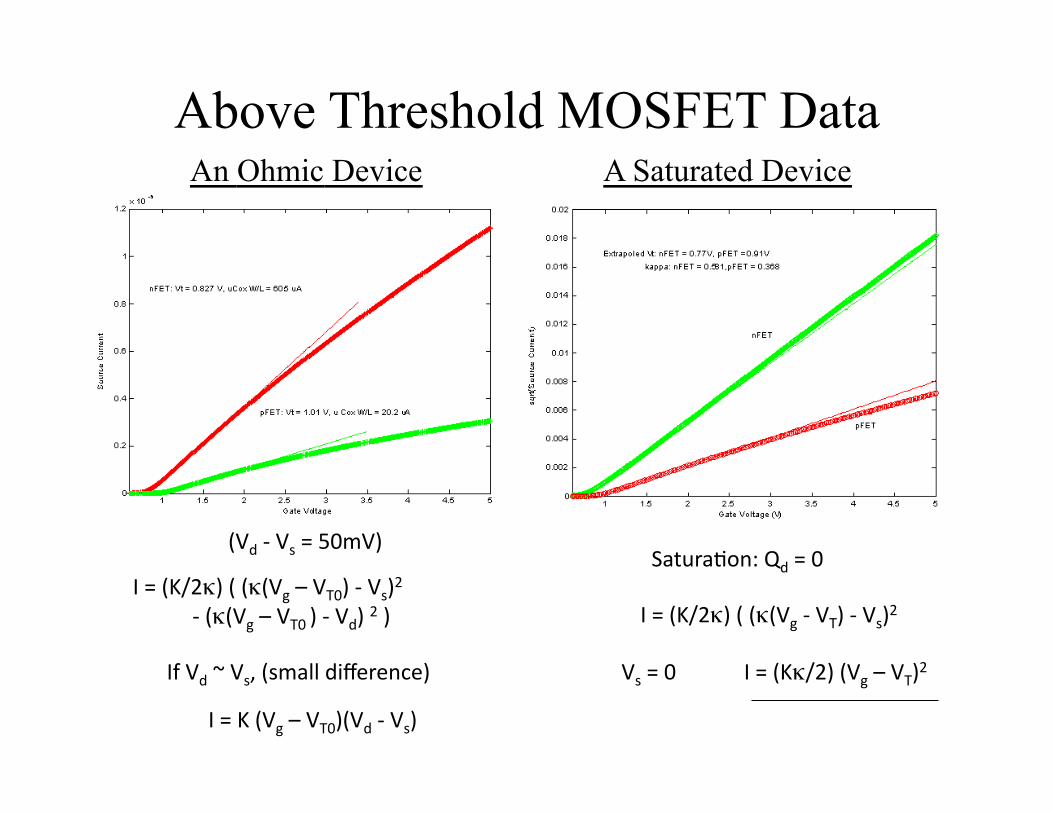
Above Threshold MOSFET Data
I = (K/2κ) ( (κ(Vg – VT0) -‐ Vs)2 -‐ (κ(Vg – VT0 ) -‐ Vd) 2 )
If Vd ~ Vs, (small difference)
(Vd -‐ Vs = 50mV)
I = K (Vg – VT0)(Vd -‐ Vs)
An Ohmic Device A Saturated Device
Satura:on: Qd = 0
I = (K/2κ) ( (κ(Vg -‐ VT) -‐ Vs)2
Vs = 0 I = (Kκ/2) (Vg – VT)2
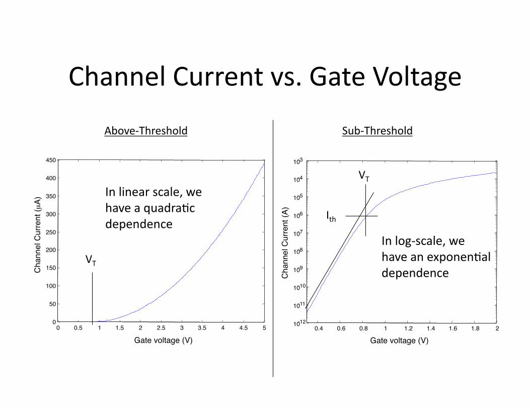
Channel Current vs. Gate Voltage
0 0.5 1 1.5 2 2.5 3 3.5 4 4.5 5 0
50
100
150
200
250
300
350
400
450
Gate voltage (V)
Cha
nnel
Cur
rent
(µA)
0.4 0.6 0.8 1 1.2 1.4 1.6 1.8 2 10 -12
10 -11
10 -10
10 -9
10 -8
10 -7
10 -6
10 -5
10 -4
10 -3
Gate voltage (V)
Cha
nnel
Cur
rent
(A)
Above-‐Threshold Sub-‐Threshold
In linear scale, we have a quadra:c dependence
In log-‐scale, we have an exponen:al dependence
VT
VT
Ith
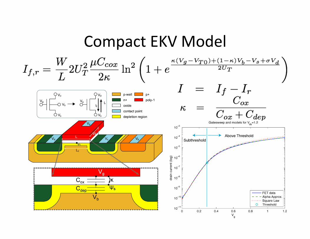
Compact EKV Model
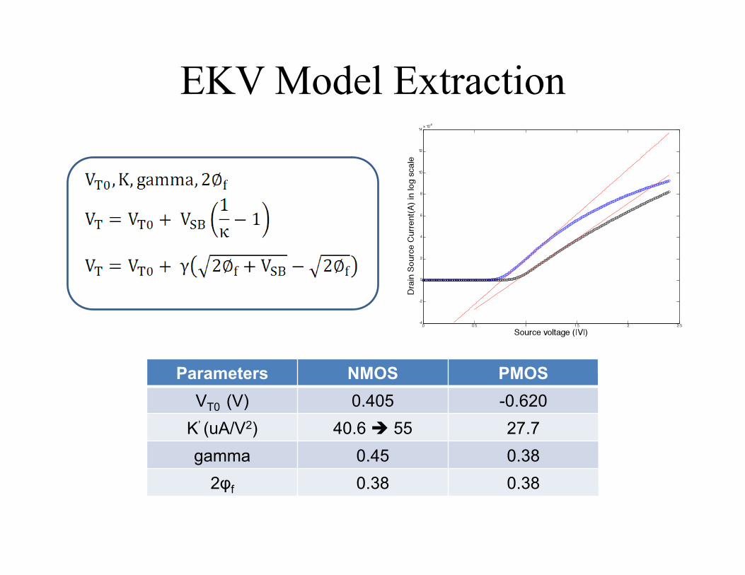
Parameters NMOS PMOS VT0 (V) 0.405 -0.620
K’ (uA/V2) 40.6 55 27.7 gamma 0.45 0.38
2φf 0.38 0.38
EKV Model Extraction
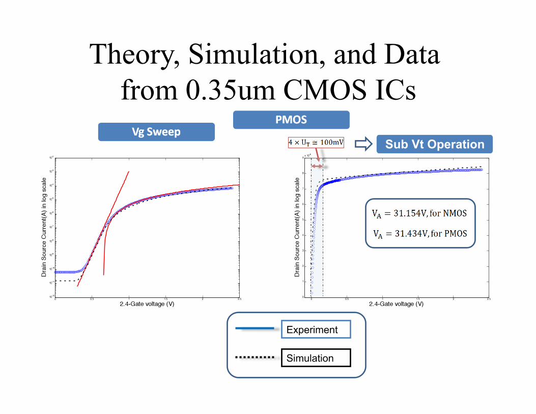
Simulation
Experiment
Sub Vt Operation
Theory, Simulation, and Data from 0.35um CMOS ICs
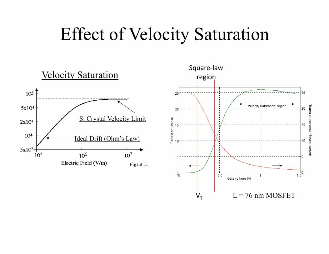
Effect of Velocity Saturation
L = 76 nm MOSFET VT
Square-‐law region Velocity Saturation
Ideal Drift (Ohm’s Law)
Si Crystal Velocity Limit
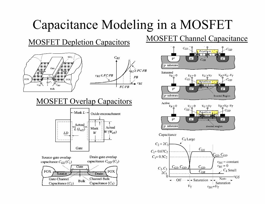
Capacitance Modeling in a MOSFET MOSFET Depletion Capacitors MOSFET Channel Capacitance
MOSFET Overlap Capacitors
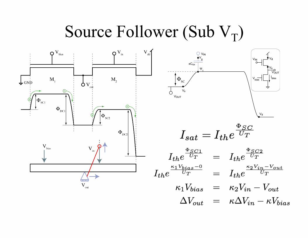
Source Follower (Sub VT)
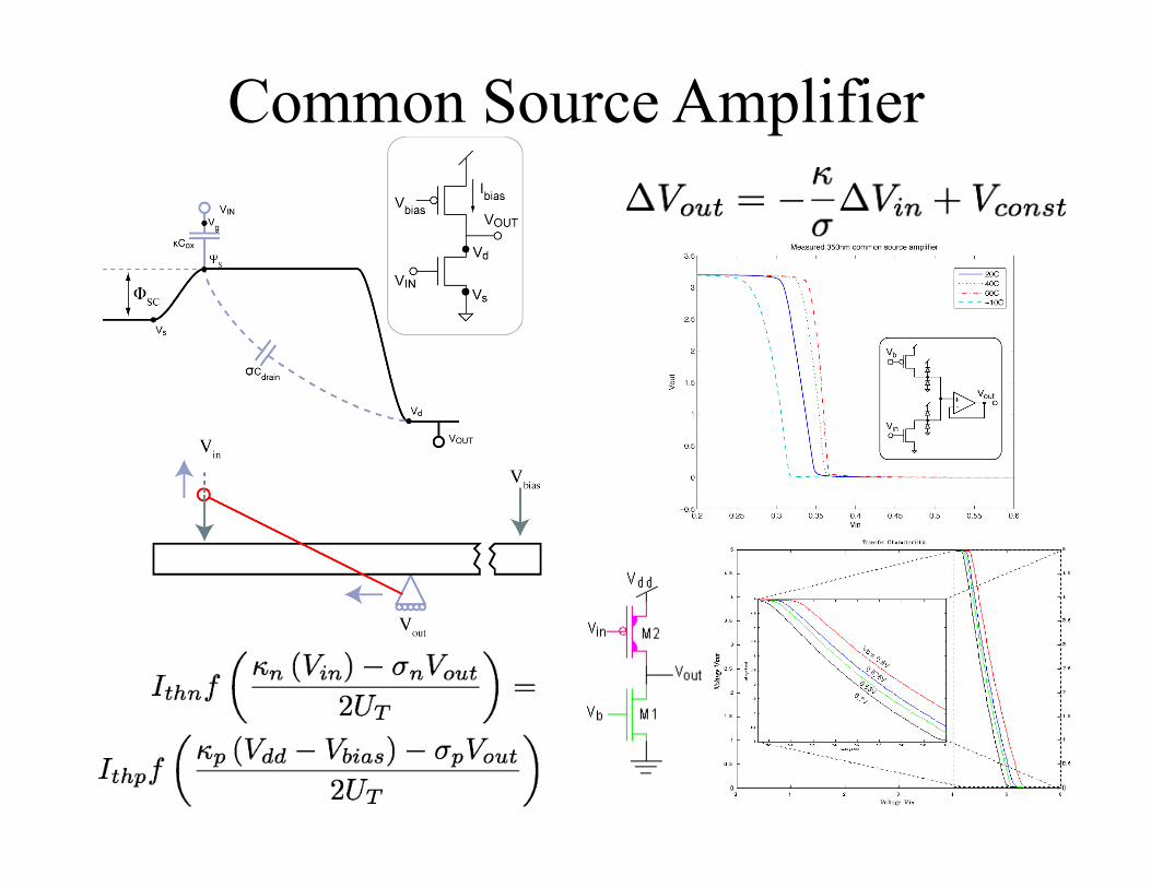
Common Source Amplifier