Embed Size (px)
Citation preview
U.S. Regional Update
2013 International Workshop on EUV Lithography
Presented by Greg Denbeaux CNSE
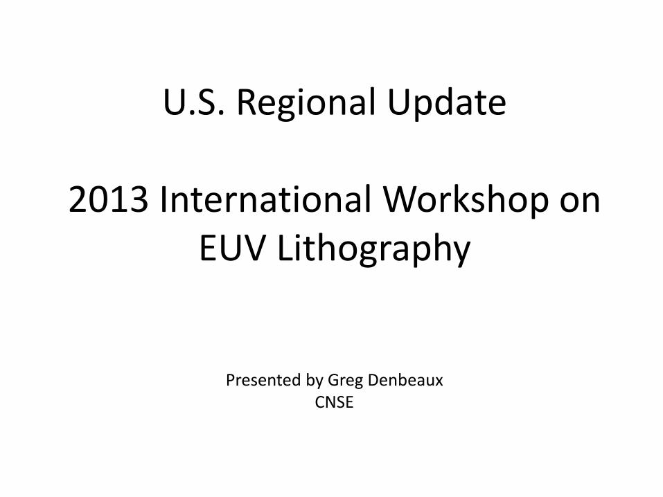
Resist-outgas testing at NIST
• NIST resist-outgas testing update
2 customer resists tested since SPIE (3/11/13)
23 total customer resists tested to date
All have passed CG
None have shown significant non-cleanables with XPS
• Ongoing work
Scaling of outgas-test CG with time & resist dose
Identifying sources of inter-facility discrepancies
Optimizing & validating relevance of “non-cleanables” portion of outgas test
Verifying EUV / e-beam correlation for “non-cleanables”
2
S. B. Hill, C. Tarrio, B. Berg, N. Faradzhev, S. Grantham and T. B. Lucatorto
3
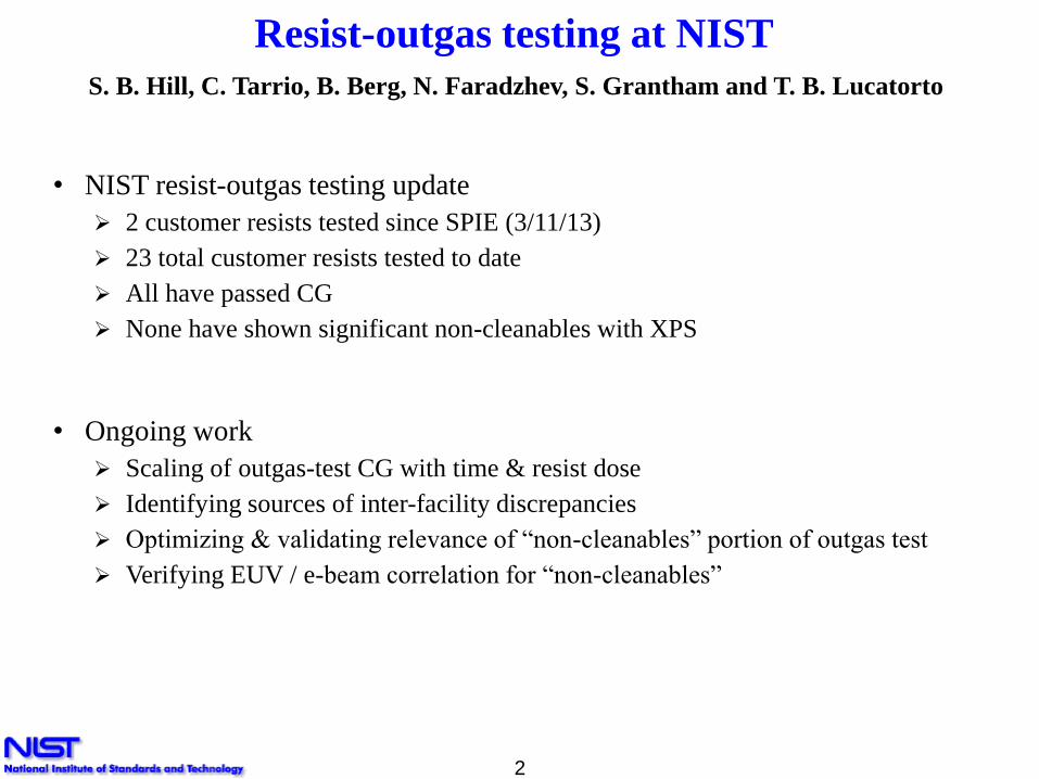
Three strategies to study non-cleanables
Spin coat
Ru-substrate
Spun films with specific chemistries: S, F, I, …
EUV & e-beam
• Species with S, F, I, …
• Pure hydrocarbon
• Vary pressure & dose Ru witness
sample
+
Witness sample in admitted gases EUV & e-beam
+ EUV
Resist-coated wafer
Witness sample in resist outgassing
Ru witness sample
• EUV resists with S, F, I, …
• Vary dose & time
• Record RGA
EUV & e-beam
Characterization of EUV/e-beam exposures
Composition: C & non-cleanables
AH cleaning rates: C & non-cleanables
Correlation with outgas RGA
AH cleaning
XPS before and
at regular intervals
during AH cleaning.
Polymers designed
with non-cleanable
elements (S, F, etc) in
specific chemical
forms.
AH cleaner in situ with XPS (coming soon)
EUVL Workshop US Regional Update
June 2013
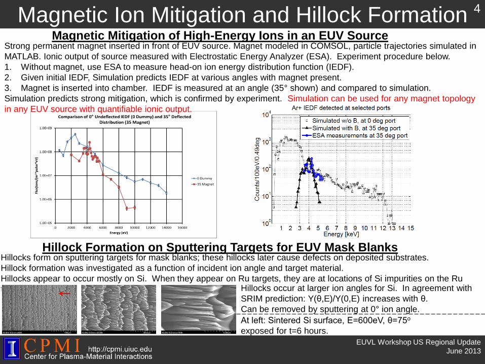
Magnetic Ion Mitigation and Hillock Formation 4
Magnetic Mitigation of High-Energy Ions in an EUV Source Strong permanent magnet inserted in front of EUV source. Magnet modeled in COMSOL, particle trajectories simulated in
MATLAB. Ionic output of source measured with Electrostatic Energy Analyzer (ESA). Experiment procedure below.
1. Without magnet, use ESA to measure head-on ion energy distribution function (IEDF).
2. Given initial IEDF, Simulation predicts IEDF at various angles with magnet present.
3. Magnet is inserted into chamber. IEDF is measured at an angle (35° shown) and compared to simulation.
Simulation predicts strong mitigation, which is confirmed by experiment. Simulation can be used for any magnet topology
in any EUV source with quantifiable ionic output.
Hillock Formation on Sputtering Targets for EUV Mask Blanks Hillocks form on sputtering targets for mask blanks; these hillocks later cause defects on deposited substrates.
Hillock formation was investigated as a function of incident ion angle and target material.
Hillocks appear to occur mostly on Si. When they appear on Ru targets, they are at locations of Si impurities on the Ru
target. Hillocks occur at larger ion angles for Si. In agreement with
SRIM prediction: Y(θ,E)/Y(0,E) increases with θ.
Can be removed by sputtering at 0° ion angle.
At left: Sintered Si surface, E=600eV, θ=75o
exposed for t=6 hours.
EUVL Workshop US Regional Update
June 2013
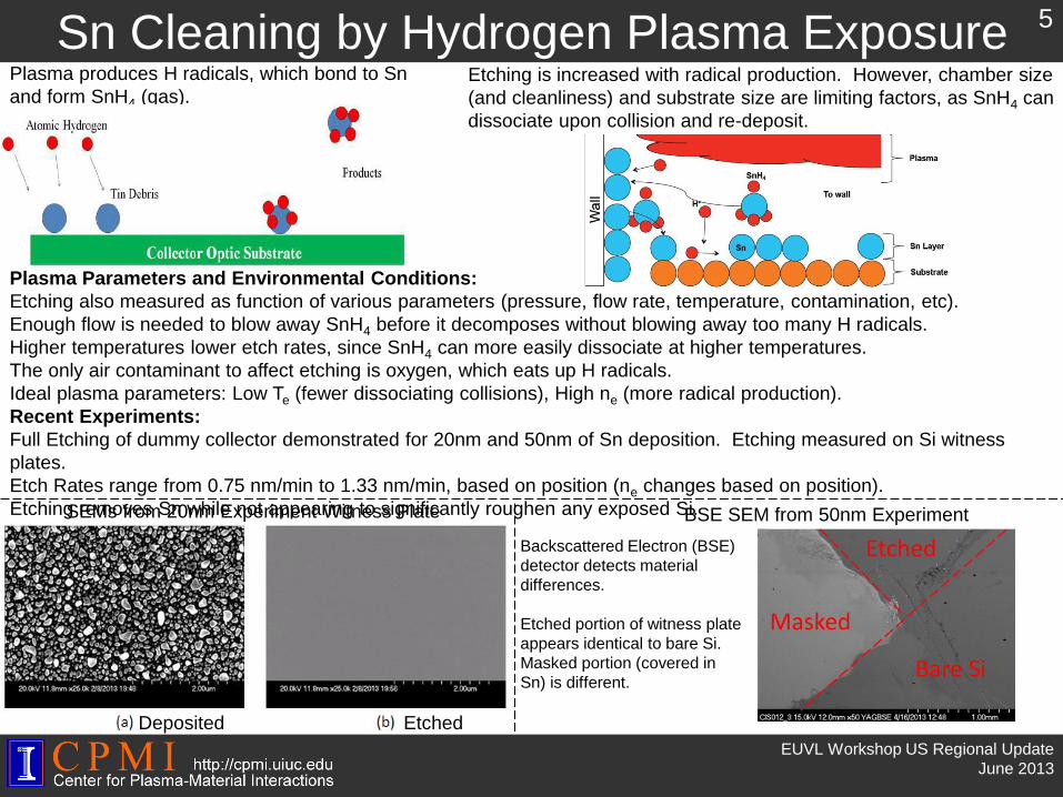
Sn Cleaning by Hydrogen Plasma Exposure 5
Plasma produces H radicals, which bond to Sn
and form SnH4 (gas). Etching is increased with radical production. However, chamber size
(and cleanliness) and substrate size are limiting factors, as SnH4 can
dissociate upon collision and re-deposit.
Plasma Parameters and Environmental Conditions:
Etching also measured as function of various parameters (pressure, flow rate, temperature, contamination, etc).
Enough flow is needed to blow away SnH4 before it decomposes without blowing away too many H radicals.
Higher temperatures lower etch rates, since SnH4 can more easily dissociate at higher temperatures.
The only air contaminant to affect etching is oxygen, which eats up H radicals.
Ideal plasma parameters: Low Te (fewer dissociating collisions), High ne (more radical production).
Recent Experiments:
Full Etching of dummy collector demonstrated for 20nm and 50nm of Sn deposition. Etching measured on Si witness
plates.
Etch Rates range from 0.75 nm/min to 1.33 nm/min, based on position (ne changes based on position).
Etching removes Sn while not appearing to significantly roughen any exposed Si.
Deposited Etched
SEMs from 20nm Experiment Witness Plate BSE SEM from 50nm Experiment
Backscattered Electron (BSE)
detector detects material
differences.
Etched portion of witness plate
appears identical to bare Si.
Masked portion (covered in
Sn) is different.
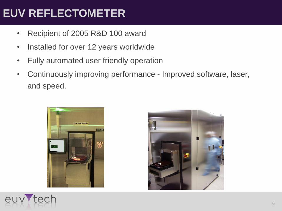
EUV REFLECTOMETER
6
• Recipient of 2005 R&D 100 award
• Installed for over 12 years worldwide
• Fully automated user friendly operation
• Continuously improving performance - Improved software, laser,
and speed.
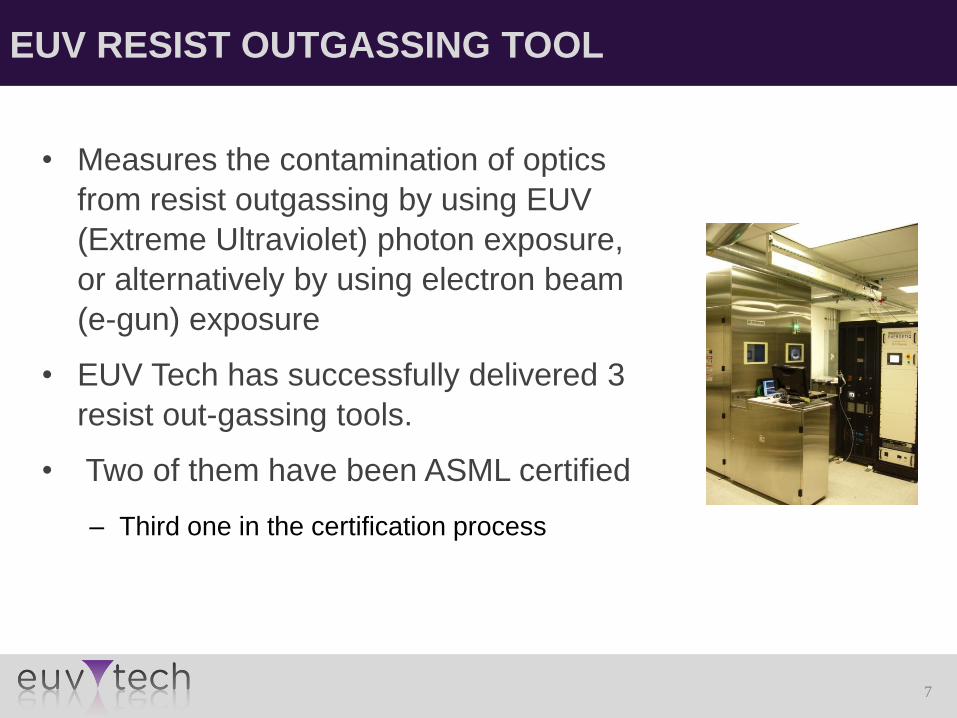
EUV RESIST OUTGASSING TOOL
7
• Measures the contamination of optics
from resist outgassing by using EUV
(Extreme Ultraviolet) photon exposure,
or alternatively by using electron beam
(e-gun) exposure
• EUV Tech has successfully delivered 3
resist out-gassing tools.
• Two of them have been ASML certified
– Third one in the certification process
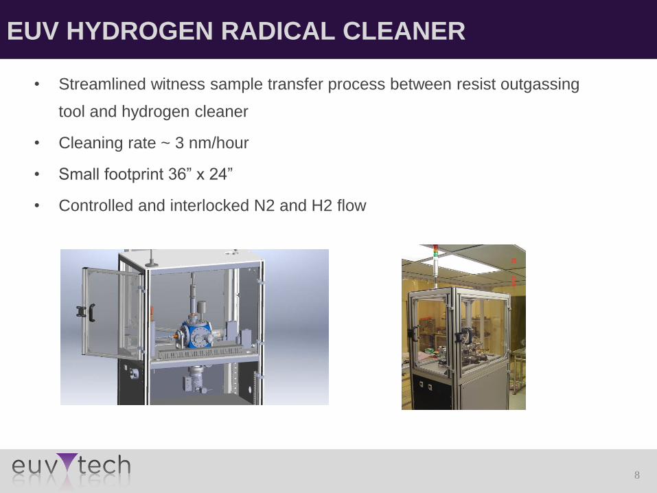
EUV HYDROGEN RADICAL CLEANER
8
• Streamlined witness sample transfer process between resist outgassing
tool and hydrogen cleaner
• Cleaning rate ~ 3 nm/hour
• Small footprint 36” x 24”
• Controlled and interlocked N2 and H2 flow
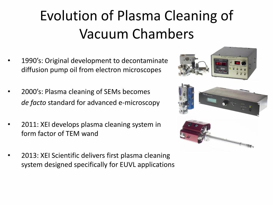
Evolution of Plasma Cleaning of Vacuum Chambers
• 1990’s: Original development to decontaminate diffusion pump oil from electron microscopes
• 2000’s: Plasma cleaning of SEMs becomes
de facto standard for advanced e-microscopy
• 2011: XEI develops plasma cleaning system in form factor of TEM wand
• 2013: XEI Scientific delivers first plasma cleaning system designed specifically for EUVL applications
ENERGETIQ Confidential • 7/7/2013 • 11
Energetiq’s Products
High-brightness, long-life light source
products
– 1nm to 2000nm wavelength
Product Applications
– EUV Lithography and Metrology
Semiconductor Manufacturing
– Soft X-Ray
Biological Imaging and Microprobe
– UV/Vis/IR Imaging and Analysis
Spectroscopy
Inspection and Metrology
LDLS™ Laser-Driven Light Sources
Electrodeless Z-Pinch™ EUV Sources
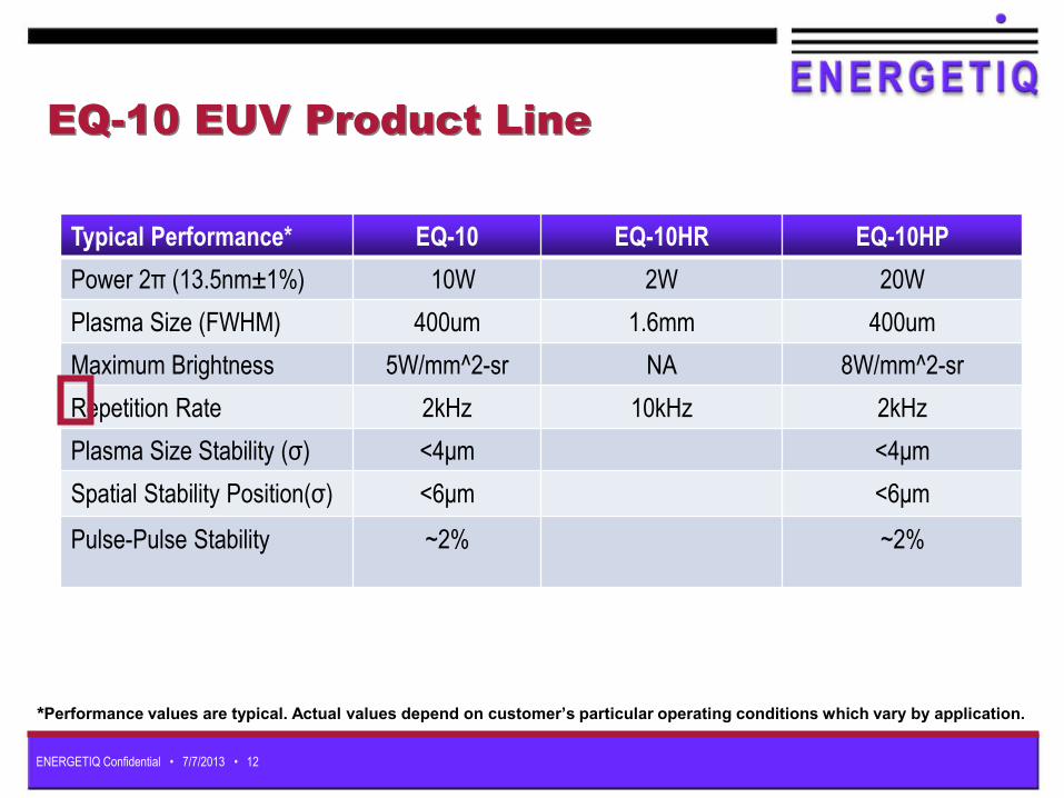
ENERGETIQ Confidential • 7/7/2013 • 12
EQ-10 EUV Product Line
Typical Performance* EQ-10 EQ-10HR EQ-10HP
Power 2π (13.5nm±1%) 10W 2W 20W
Plasma Size (FWHM) 400um 1.6mm 400um
Maximum Brightness 5W/mm^2-sr NA 8W/mm^2-sr
Repetition Rate 2kHz 10kHz 2kHz
Plasma Size Stability (σ) <4μm <4μm
Spatial Stability Position(σ) <6μm <6μm
Pulse-Pulse Stability ~2% ~2%
*Performance values are typical. Actual values depend on customer’s particular operating conditions which vary by application.
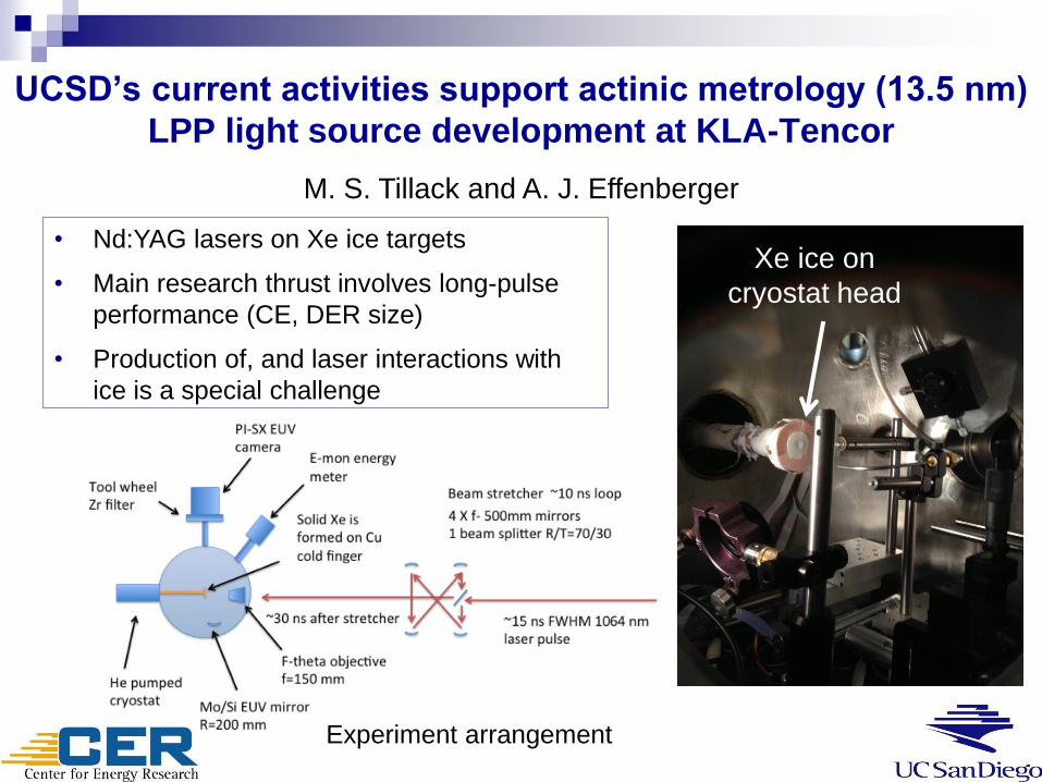
UCSD’s current activities support actinic metrology (13.5 nm)
LPP light source development at KLA-Tencor
• Nd:YAG lasers on Xe ice targets
• Main research thrust involves long-pulse
performance (CE, DER size)
• Production of, and laser interactions with
ice is a special challenge
M. S. Tillack and A. J. Effenberger
Xe ice on
cryostat head
Experiment arrangement
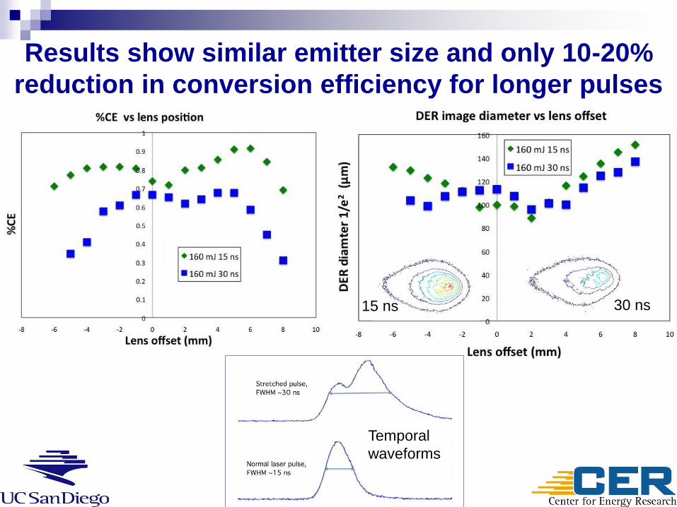
Results show similar emitter size and only 10-20%
reduction in conversion efficiency for longer pulses
15 ns 30 ns
Temporal
waveforms
7 July 2013 CONFIDENTIAL © 2013 Cymer, LLC
15
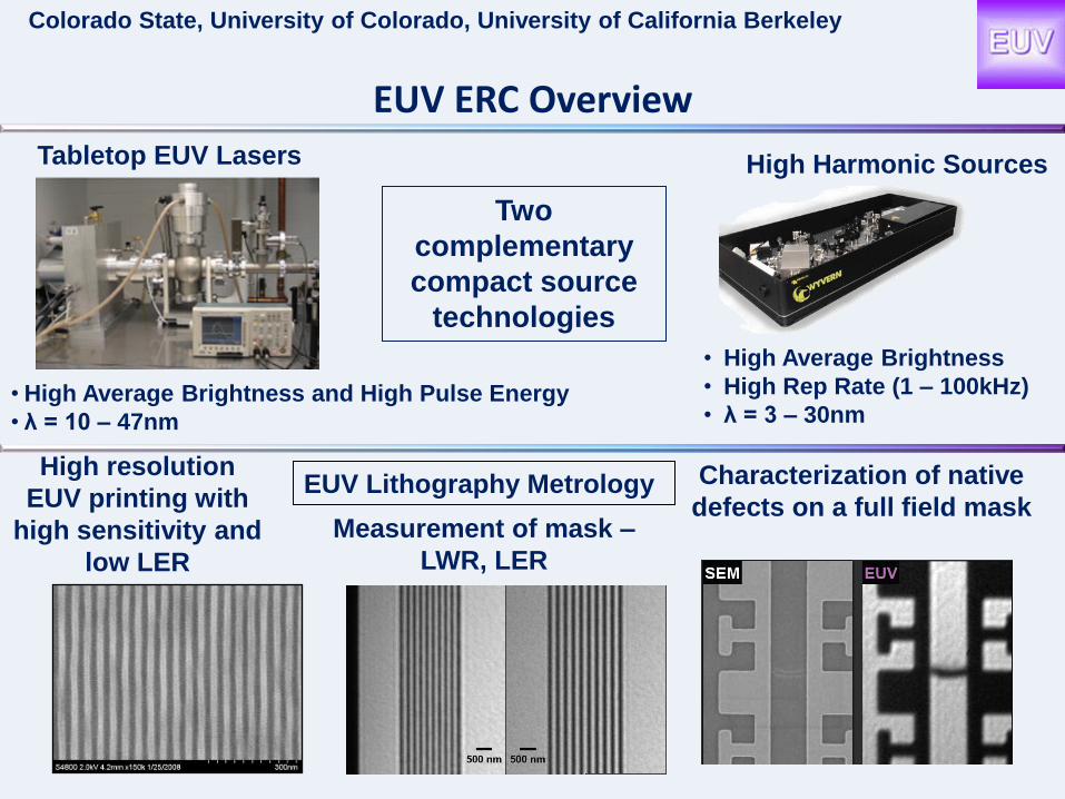
EUV ERC Overview
20 microwatt at 13.9nm
Tabletop EUV Lasers High Harmonic Sources
• High Average Brightness and High Pulse Energy
• λ = 10 – 47nm
• High Average Brightness
• High Rep Rate (1 – 100kHz)
• λ = 3 – 30nm
Two
complementary
compact source
technologies
High resolution
EUV printing with
high sensitivity and
low LER
Characterization of native
defects on a full field mask Measurement of mask –
LWR, LER
EUV Lithography Metrology
Colorado State, University of Colorado, University of California Berkeley
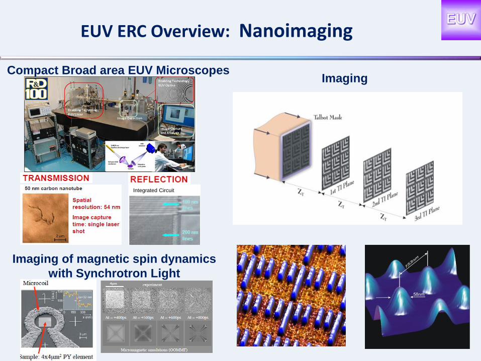
EUV ERC Overview: Nanoimaging
Compact Broad area EUV Microscopes
Integrated Circuit
Imaging of magnetic spin dynamics
with Synchrotron Light
Imaging
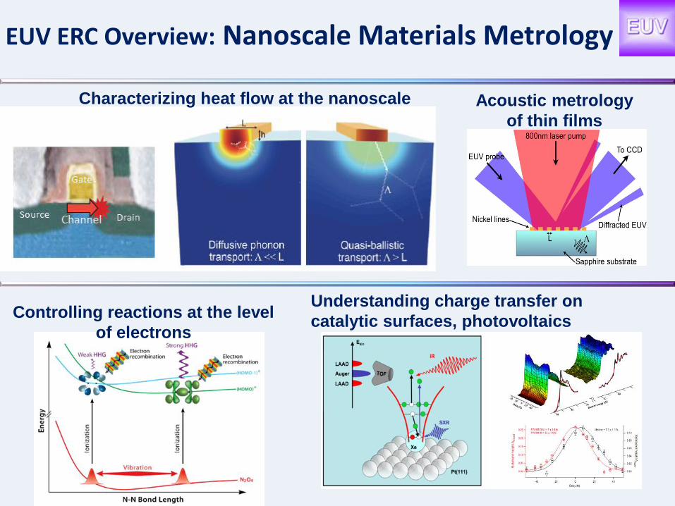
EUV ERC Overview: Nanoscale Materials Metrology
Characterizing heat flow at the nanoscale Acoustic metrology
of thin films
Controlling reactions at the level
of electrons
Understanding charge transfer on
catalytic surfaces, photovoltaics
0.98
0.99
1.00
1.01
1.02
0 50 100 150
measured
P-V = 0.04 %
AFE = 0.033 nm rms
= 87
MET5 M2
spherical test mirror
Mo/Si multilayer
goal
M2 clear aperture
Radial position r (mm)
No
rma
lize
d t
hic
kn
ess
profi
le
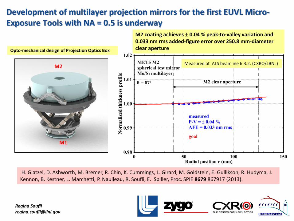
M2 coating achieves 0.04 % peak-to-valley variation and 0.033 nm rms added-figure error over 250.8 mm-diameter clear aperture
Development of multilayer projection mirrors for the first EUVL Micro-Exposure Tools with NA = 0.5 is underway
M2
M1
Opto-mechanical design of Projection Optics Box
Measured at ALS beamline 6.3.2. (CXRO/LBNL)
H. Glatzel, D. Ashworth, M. Bremer, R. Chin, K. Cummings, L. Girard, M. Goldstein, E. Gullikson, R. Hudyma, J. Kennon, B. Kestner, L. Marchetti, P. Naulleau, R. Soufli, E. Spiller, Proc. SPIE 8679 867917 (2013).
Regina Soufli [email protected]
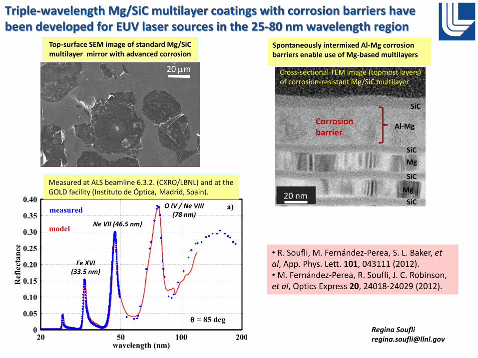
Triple-wavelength Mg/SiC multilayer coatings with corrosion barriers have been developed for EUV laser sources in the 25-80 nm wavelength region
0
0.05
0.10
0.15
0.20
0.25
0.30
0.35
0.40
20 50 100 200
= 85 deg
a)measured
model
wavelength (nm)
Ref
lect
an
ce
O IV / Ne VIII (78 nm)
Ne VII (46.5 nm)
Fe XVI (33.5 nm)
Spontaneously intermixed Al-Mg corrosion barriers enable use of Mg-based multilayers
Top-surface SEM image of standard Mg/SiC multilayer mirror with advanced corrosion
20 m
Al-Mg
SiC
SiC
Mg
SiC
Mg
Cross-sectional TEM image (topmost layers) of corrosion-resistant Mg/SiC multilayer
SiC 20 nm
Corrosion barrier
Measured at ALS beamline 6.3.2. (CXRO/LBNL) and at the GOLD facility (Instituto de Óptica, Madrid, Spain).
• R. Soufli, M. Fernández-Perea, S. L. Baker, et al, App. Phys. Lett. 101, 043111 (2012). • M. Fernández-Perea, R. Soufli, J. C. Robinson, et al, Optics Express 20, 24018-24029 (2012).
Regina Soufli [email protected]
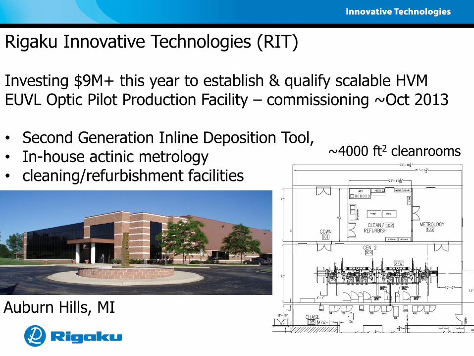
Rigaku Innovative Technologies (RIT) Investing $9M+ this year to establish & qualify scalable HVM EUVL Optic Pilot Production Facility – commissioning ~Oct 2013 • Second Generation Inline Deposition Tool, • In-house actinic metrology • cleaning/refurbishment facilities
Auburn Hills, MI
~4000 ft2 cleanrooms
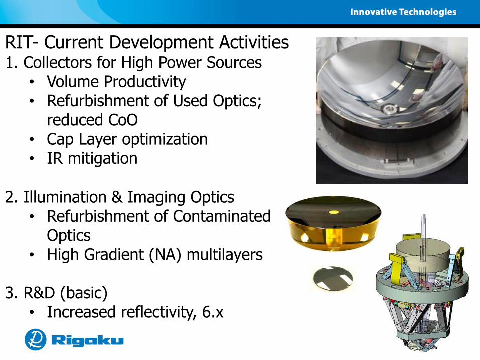
RIT- Current Development Activities 1. Collectors for High Power Sources
• Volume Productivity • Refurbishment of Used Optics;
reduced CoO • Cap Layer optimization • IR mitigation
2. Illumination & Imaging Optics
• Refurbishment of Contaminated Optics
• High Gradient (NA) multilayers
3. R&D (basic) • Increased reflectivity, 6.x
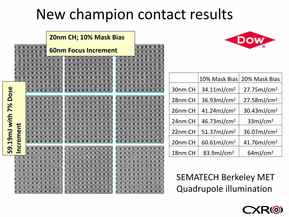
New champion contact results
10% Mask Bias 20% Mask Bias
30nm CH 34.11mJ/cm2 27.75mJ/cm2
28nm CH 36.93mJ/cm2 27.58mJ/cm2
26nm CH 41.24mJ/cm2 30.43mJ/cm2
24nm CH 46.73mJ/cm2 33mJ/cm2
22nm CH 51.37mJ/cm2 36.07mJ/cm2
20nm CH 60.61mJ/cm2 41.76mJ/cm2
18nm CH 83.9mJ/cm2 64mJ/cm2
20nm CH; 10% Mask Bias
60nm Focus Increment
59
.19
mJ
wit
h 7
% D
ose
In
cre
me
nt
SEMATECH Berkeley MET Quadrupole illumination
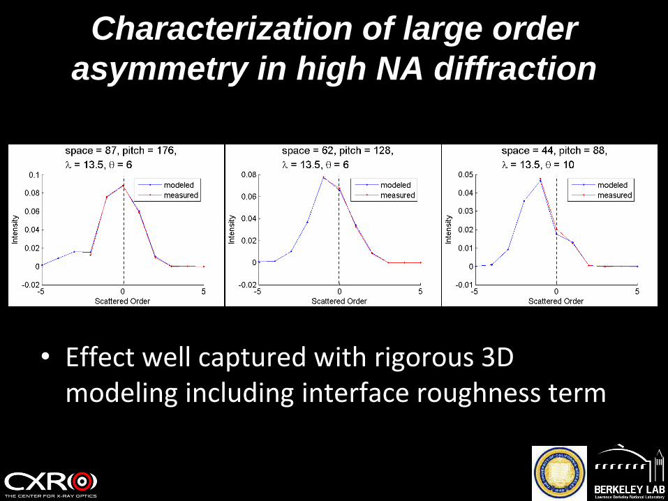
Characterization of large order
asymmetry in high NA diffraction
• Effect well captured with rigorous 3D modeling including interface roughness term
65-nm hp
(16.25) 55-nm hp
(13.75)
60-nm hp
(15.00)
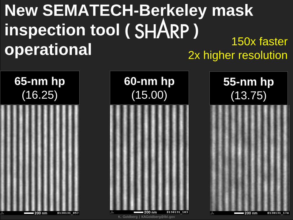
New SEMATECH-Berkeley mask
inspection tool ( )
operational 150x faster
2x higher resolution
K. Goldberg | [email protected]
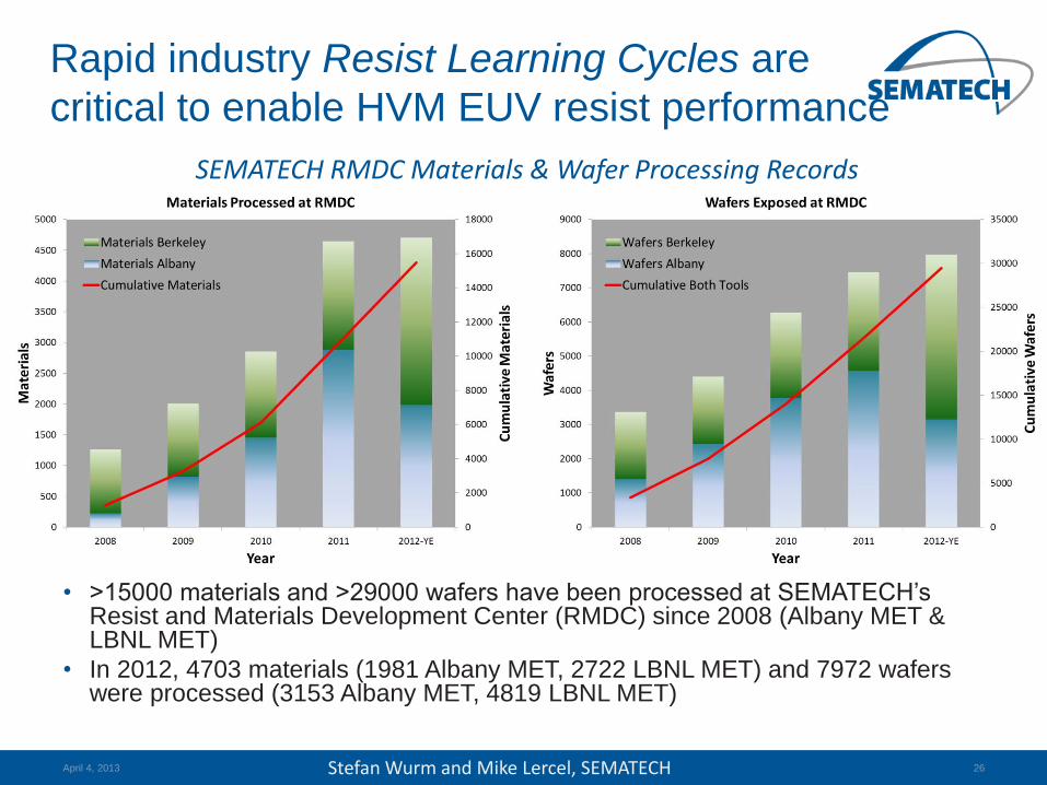
Rapid industry Resist Learning Cycles are
critical to enable HVM EUV resist performance
26
• >15000 materials and >29000 wafers have been processed at SEMATECH’s Resist and Materials Development Center (RMDC) since 2008 (Albany MET & LBNL MET)
• In 2012, 4703 materials (1981 Albany MET, 2722 LBNL MET) and 7972 wafers were processed (3153 Albany MET, 4819 LBNL MET)
April 4, 2013
SEMATECH RMDC Materials & Wafer Processing Records
Stefan Wurm and Mike Lercel, SEMATECH
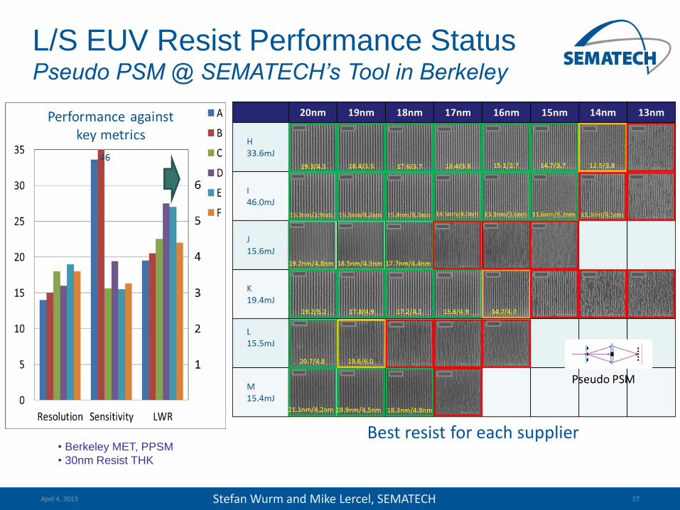
L/S EUV Resist Performance Status Pseudo PSM @ SEMATECH’s Tool in Berkeley
• Berkeley MET, PPSM
• 30nm Resist THK
Best resist for each supplier
April 4, 2013 27 Stefan Wurm and Mike Lercel, SEMATECH
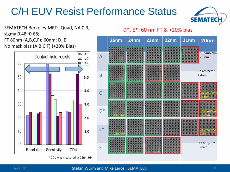
SEMATECH Berkeley MET: Quad, NA 0.3, sigma 0.48~0.68; FT 80nm (A,B,C,F); 60nm; D, E No mask bias (A,B,C,F) (+20% Bias)
26nm 24nm 23nm 22nm 21nm 20nm
A
B
C
D*
E*
F
59.5mJ/cm2 2.5nm
52.4mJ/cm2 2.4nm
36.3mJ/cm2 3.3nm
23.9mJ/cm2 3.0nm
* CDU was measured at 26nm HP
1.0
2.0
3.0
4.0
April 4, 2013
5.0
25nmHP
33.5mJ/cm2 3.1nm
21.0mJ/cm2 5.2nm 25nmHP
D*, E*: 60 nm FT & +20% bias
C/H EUV Resist Performance Status
28 Stefan Wurm and Mike Lercel, SEMATECH
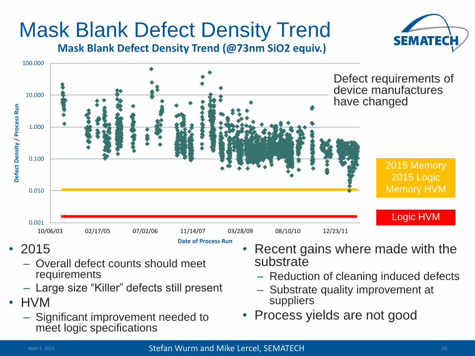
Mask Blank Defect Density Trend
• 2015 – Overall defect counts should meet
requirements
– Large size “Killer” defects still present
• HVM – Significant improvement needed to
meet logic specifications
April 4, 2013
0.001
0.010
0.100
1.000
10.000
100.000
10/06/03 02/17/05 07/02/06 11/14/07 03/28/09 08/10/10 12/23/11
De
fect
De
nsi
ty /
Pro
cess
Ru
n
Date of Process Run
Mask Blank Defect Density Trend (@73nm SiO2 equiv.)
2015 Memory
2015 Logic
Memory HVM
Logic HVM
Defect requirements of device manufactures have changed
29
• Recent gains where made with the substrate – Reduction of cleaning induced defects
– Substrate quality improvement at suppliers
• Process yields are not good
Stefan Wurm and Mike Lercel, SEMATECH
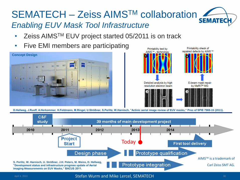
SEMATECH – Zeiss AIMSTM collaboration Enabling EUV Mask Tool Infrastructure
April 4, 2013
• Zeiss AIMSTM EUV project started 05/2011 is on track
• Five EMI members are participating
AIMS is a trademark of
Carl Zeiss SMT AG. S. Perlitz, W. Harnisch, U. Strößner, J.H. Peters, M. Weiss, D. Hellweg,
”Development status and infrastructure progress update of Aerial
imaging Measurements on EUV Masks,“ BACUS 2011.
Concept Design
D.Hellweg, J.Ruoff, A.Herkommer, H.Feldmann, M.Ringel, U.Strößner, S.Perlitz, W.Harnisch, ”Actinic aerial image review of EUV masks,“ Proc of SPIE 7969-15 (2011).
30
Today
Stefan Wurm and Mike Lercel, SEMATECH
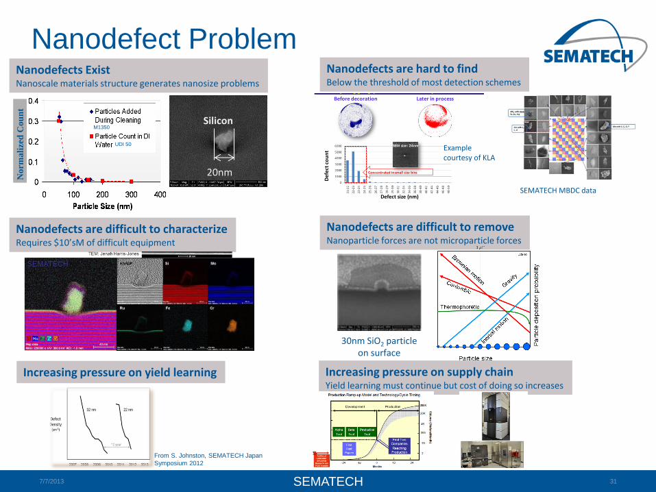
Nanodefect Problem N
orm
ali
zed
Cou
nt
M1350
UDI 50
Silicon
20nm
Nanodefects Exist Nanoscale materials structure generates nanosize problems
Nanodefects are hard to find Below the threshold of most detection schemes What drives our inspection roadmap?
2. Early flagging (before decoration)
Def
ect
cou
nt
Concentrated in small size bins
SEM size: 24nm
Later in processBefore decoration
Defect size (nm)
Example courtesy of KLA
Nanodefects are difficult to characterize Requires $10’sM of difficult equipment
SEMATECH MBDC data
Nanodefects are difficult to remove Nanoparticle forces are not microparticle forces
30nm SiO2 particle on surface
Increasing pressure on yield learning Increasing pressure on supply chain Yield learning must continue but cost of doing so increases
7/7/2013 SEMATECH 31
From S. Johnston, SEMATECH Japan
Symposium 2012
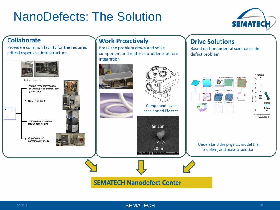
NanoDefects: The Solution
Collaborate Provide a common facility for the required critical expensive infrastructure
Work Proactively Break the problem down and solve component and material problems before integration
Drive Solutions Based on fundamental science of the defect problem
Defect inspection
Silicon
20nm
Component level accelerated life test
Understand the physics, model the problem, and make a solution
-0.1
0.0
0.1
0.2
0.3
0.4
0.5
0.6
0.7
0.8
25 Cleaning
63 Cleaning
63 Cleaning
65 Cleaning
Dec 10Sept - Nov,10Q2 - Aug,10
Adder count
Q1,10
Tool Component
improvement
Filter
Install
Best Adder
Data
-0.1
0.0
0.1
0.2
0.3
0.4
0.5
0.6
0.7
0.8
25 Cleaning
63 Cleaning
63 Cleaning
65 Cleaning
Dec 10Sept - Nov,10Q2 - Aug,10
Adder count
Q1,10
Tool Component
improvement
Filter
Install
Best Adder
Data
-0.1
0.0
0.1
0.2
0.3
0.4
0.5
0.6
0.7
0.8
25 Cleaning
63 Cleaning
63 Cleaning
65 Cleaning
Dec 10Sept - Nov,10Q2 - Aug,10
Adder count
Q1,10
Tool Component
improvement
Filter
Install
Best Adder
Data
-0.1
0.0
0.1
0.2
0.3
0.4
0.5
0.6
0.7
0.8
25 Cleaning
63 Cleaning
63 Cleaning
65 Cleaning
Dec 10Sept - Nov,10Q2 - Aug,10
Adder count
Q1,10
Tool Component
improvement
Filter
Install
Best Adder
Data
SEMATECH Nanodefect Center
7/7/2013 SEMATECH 32