Embed Size (px)
Citation preview
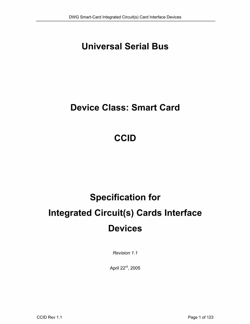
DWG Smart-Card Integrated Circuit(s) Card Interface Devices
Universal Serial Bus
Device Class: Smart Card
CCID
Specification for Integrated Circuit(s) Cards Interface
Devices
Revision 1.1
April 22rd, 2005
CCID Rev 1.1 Page 1 of 123
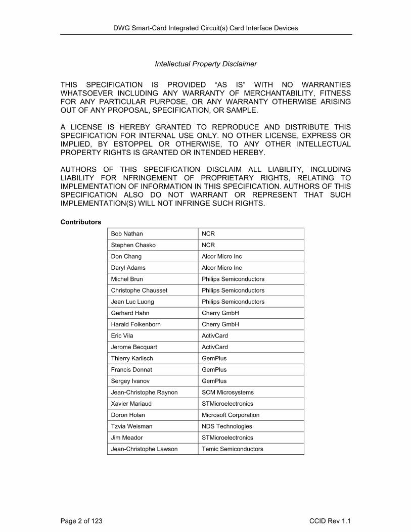
DWG Smart-Card Integrated Circuit(s) Card Interface Devices
Intellectual Property Disclaimer
THIS SPECIFICATION IS PROVIDED “AS IS” WITH NO WARRANTIES WHATSOEVER INCLUDING ANY WARRANTY OF MERCHANTABILITY, FITNESS FOR ANY PARTICULAR PURPOSE, OR ANY WARRANTY OTHERWISE ARISING OUT OF ANY PROPOSAL, SPECIFICATION, OR SAMPLE. A LICENSE IS HEREBY GRANTED TO REPRODUCE AND DISTRIBUTE THIS SPECIFICATION FOR INTERNAL USE ONLY. NO OTHER LICENSE, EXPRESS OR IMPLIED, BY ESTOPPEL OR OTHERWISE, TO ANY OTHER INTELLECTUAL PROPERTY RIGHTS IS GRANTED OR INTENDED HEREBY. AUTHORS OF THIS SPECIFICATION DISCLAIM ALL LIABILITY, INCLUDING LIABILITY FOR NFRINGEMENT OF PROPRIETARY RIGHTS, RELATING TO IMPLEMENTATION OF INFORMATION IN THIS SPECIFICATION. AUTHORS OF THIS SPECIFICATION ALSO DO NOT WARRANT OR REPRESENT THAT SUCH IMPLEMENTATION(S) WILL NOT INFRINGE SUCH RIGHTS. Contributors
Bob Nathan NCR
Stephen Chasko NCR
Don Chang Alcor Micro Inc
Daryl Adams Alcor Micro Inc
Michel Brun Philips Semiconductors
Christophe Chausset Philips Semiconductors
Jean Luc Luong Philips Semiconductors
Gerhard Hahn Cherry GmbH
Harald Folkenborn Cherry GmbH
Eric Vila ActivCard
Jerome Becquart ActivCard
Thierry Karlisch GemPlus
Francis Donnat GemPlus
Sergey Ivanov GemPlus
Jean-Christophe Raynon SCM Microsystems
Xavier Mariaud STMicroelectronics
Doron Holan Microsoft Corporation
Tzvia Weisman NDS Technologies
Jim Meador STMicroelectronics
Jean-Christophe Lawson Temic Semiconductors
Page 2 of 123 CCID Rev 1.1
DWG Smart-Card Integrated Circuit(s) Card Interface Devices
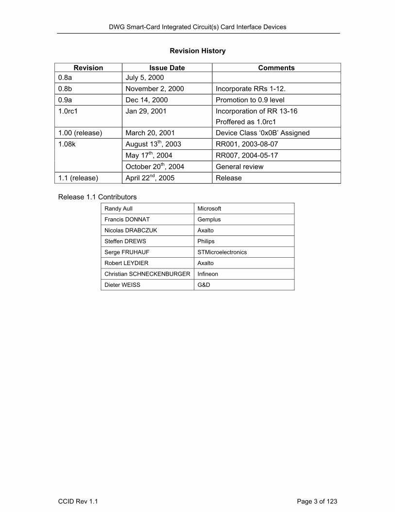
Revision History
Revision Issue Date Comments 0.8a July 5, 2000 0.8b November 2, 2000 Incorporate RRs 1-12. 0.9a Dec 14, 2000 Promotion to 0.9 level 1.0rc1 Jan 29, 2001 Incorporation of RR 13-16
Proffered as 1.0rc1 1.00 (release) March 20, 2001 Device Class ‘0x0B’ Assigned
August 13th, 2003 RR001, 2003-08-07 May 17th, 2004 RR007, 2004-05-17
1.08k
October 20th, 2004 General review 1.1 (release) April 22nd, 2005 Release Release 1.1 Contributors
Randy Aull Microsoft
Francis DONNAT Gemplus
Nicolas DRABCZUK Axalto
Steffen DREWS Philips
Serge FRUHAUF STMicroelectronics
Robert LEYDIER Axalto
Christian SCHNECKENBURGER Infineon
Dieter WEISS G&D
CCID Rev 1.1 Page 3 of 123
DWG Smart-Card Integrated Circuit(s) Card Interface Devices
Contents 1 Introduction ...................................................................................................................6 1.1 Related Documents..................................................................................................... 6 1.2 Terms and Abbreviations ............................................................................................ 6 1.3 Document Conventions ............................................................................................... 9 2 Overview ..................................................................................................................... 10 3 CCID Functional Characteristics ................................................................................. 11 3.1 Communication pipes................................................................................................ 11
3.1.1 Control pipe........................................................................................................ 11 3.1.2 Interrupt pipe...................................................................................................... 11 3.1.3 Bulk-in, Bulk-out pipes ....................................................................................... 12
3.2 Protocol and parameters selection............................................................................ 13 3.2.1 TPDU level of exchange .................................................................................... 13 3.2.2 APDU level of exchange .................................................................................... 14 3.2.3 Character level of exchange .............................................................................. 14
3.3 Suspend Behavior ..................................................................................................... 15 4 Standard USB Descriptors .......................................................................................... 16 4.1 Device ....................................................................................................................... 16 4.2 Configuration ............................................................................................................. 16 4.3 Interface .................................................................................................................... 16 5 Smart Card Device Class ............................................................................................ 17 5.1 Descriptor .................................................................................................................. 17 5.2 CCID Endpoints......................................................................................................... 20
5.2.1 Bulk-OUT Endpoint ............................................................................................ 21 5.2.2 Bulk-IN Endpoint ................................................................................................ 21 5.2.3 Interrupt-IN Endpoint.......................................................................................... 22
5.3 CCID Class-Specific Request ................................................................................... 23 5.3.1 ABORT............................................................................................................... 23 5.3.2 GET_CLOCK_FREQUENCIES ......................................................................... 24 5.3.3 GET_DATA_RATES .......................................................................................... 24
6 CCID Messages .......................................................................................................... 25 6.1 Command Pipe, Bulk-OUT Messages ...................................................................... 26
6.1.1 PC_to_RDR_IccPowerOn.................................................................................. 26 6.1.2 PC_to_RDR_IccPowerOff.................................................................................. 28 6.1.3 PC_to_RDR_GetSlotStatus ............................................................................... 29 6.1.4 PC_to_RDR_XfrBlock........................................................................................ 30 6.1.5 PC_to_RDR_GetParameters............................................................................. 31 6.1.6 PC_to_RDR_ResetParameters ......................................................................... 32 6.1.7 PC_to_RDR_SetParameters ............................................................................. 32 6.1.8 PC_to_RDR_Escape ......................................................................................... 35 6.1.9 PC_to_RDR_IccClock........................................................................................ 36 6.1.10 PC_to_RDR_T0APDU ....................................................................................... 36 6.1.11 PC_to_RDR_Secure.......................................................................................... 38 6.1.12 PC_to_RDR_Mechanical ................................................................................... 46 6.1.13 PC_to_RDR_Abort............................................................................................. 47 6.1.14 PC_to_RDR_SetDataRateAndClockFrequency ................................................ 47
6.2 Response Pipe, Bulk-IN Messages........................................................................... 48 6.2.1 RDR_to_PC_DataBlock..................................................................................... 49 6.2.2 RDR_to_PC_SlotStatus:.................................................................................... 50
Page 4 of 123 CCID Rev 1.1
DWG Smart-Card Integrated Circuit(s) Card Interface Devices
6.2.3 RDR_to_PC_Parameters................................................................................... 51 6.2.4 RDR_to_PC_Escape ......................................................................................... 53 6.2.5 RDR_to_PC_DataRateAndClockFrequency...................................................... 53 6.2.6 Reporting Slot Error and Slot Status registers in Bulk-IN messages ................. 54 6.2.7 Failure of a command ........................................................................................ 55
6.3 Interrupt-IN Messages............................................................................................... 56 6.3.1 RDR_to_PC_NotifySlotChange ......................................................................... 56 6.3.2 RDR_to_PC_HardwareError.............................................................................. 57
7 Examples of message exchanges............................................................................... 58 7.1 Common Behavior..................................................................................................... 58 7.2 Character Level ......................................................................................................... 61 7.3 APDU Level............................................................................................................... 69 7.4 TPDU Level ............................................................................................................... 80 8 Examples of PIN Management.................................................................................... 87 8.1 PIN Verification.......................................................................................................... 87
8.1.1 PIN uses a binary format conversion ................................................................. 87 8.1.2 PIN uses a shift rotation format conversion. ...................................................... 89 8.1.3 PIN uses a BCD format conversion with PIN length insertion ........................... 91 8.1.4 PIN uses BCD, right justification and a control field........................................... 93 8.1.5 PIN uses an ASCII format conversion with padding. ......................................... 95
8.2 PIN Modification ........................................................................................................ 97 8.2.1 Change PIN ASCII format (8-byte long)............................................................ 97 8.2.2 PIN uses an ASCII format conversion with PIN length management. ............... 99 8.2.3 Character Level, Protocol T = 0, sequence for PIN verification ....................... 102
9 Sample diagrams based on dwFeatures................................................................... 103 9.1 Definition of dwFeatures fields ................................................................................ 103 9.2 ICC ATRs used in these diagrams .......................................................................... 104 9.3 Voltage management .............................................................................................. 105
9.3.1 Class AB, ATR1, Feature 1.............................................................................. 105 9.3.2 Class B, ATR1, Feature 1 ................................................................................ 106 9.3.3 Class AB, ATR1, Feature 2, 3, 4, 5 and Feature 5 .......................................... 107 9.3.4 Class AB, ATR2, Feature 2, 3, 4 and Feature 5 .............................................. 108
9.4 Management of Rate and protocol .......................................................................... 109 9.4.1 Fixed rate (= ATR), ATR 2, Feature1, 2 and Feature 3 ................................... 109 9.4.2 High speed, ATR 4, Feature 1 or Feature 2..................................................... 110 9.4.3 Fixed rate (= ATR), ATR 2, Feature 4 or Feature 5 ......................................... 111 9.4.4 Fixed rate (= ATR), ATR 2, Feature 6.............................................................. 112 9.4.5 Fixed rate (= ATR), ATR 3, Feature 1.............................................................. 113 9.4.6 High speed, ATR 3, Feature1 .......................................................................... 114 9.4.7 High speed, ATR 3, Feature 2 or Feature 3..................................................... 115 9.4.8 High speed, ATR 3, Feature 4 ......................................................................... 116 9.4.9 High speed, ATR 3, Feature 5 ......................................................................... 117 9.4.10 High speed, ATR 3, Feature 6 ......................................................................... 118 9.4.11 High speed, “EMV like”, Cold ATR: ATR1, Warm ATR: ATR4, Feature 1 ....... 120
9.5 Automatic IFSD management ................................................................................. 121 9.5.1 Large IFSD, ATR4, Feature 1 or Feature 2 ..................................................... 121 9.5.2 Large IFSD, ATR4, Feature 4 .......................................................................... 122
CCID Rev 1.1 Page 5 of 123
DWG Smart-Card Integrated Circuit(s) Card Interface Devices 1 Introduction This document describes proposed requirements and specifications for Universal Serial Bus (USB) devices that interface with Integrated Circuit(s) Cards or act as interfaces with Integrated Circuit(s) Cards. 1.1 Related Documents The following related documents are available from WWW.USB.ORG
• Universal Serial Bus Specification 2.0 (also referred to as the USB specification), April 27, 2000
• Universal Serial Bus Common Class Specification 1.0, December 16, 1997
The following document is available from WWW.PCSCWORKGROUP.COM • Interoperability Specification for ICCs and Personal Computer Systems, Draft
Revision 1.0, December 1997 The following related documents can be ordered through WWW.ANSI.ORG
• ISO/IEC 7816-1; Identification Cards – Integrated circuit(s) cards with contacts Part 1: Physical Characteristics
• ISO/IEC 7816-2; Identification Cards – Integrated circuit(s) cards with contacts Part 2: Dimensions and Locations of the contacts
• ISO/IEC 7816-3; Identification Cards – Integrated circuit(s) cards with contacts Part 3: Electronic signals and transmission protocols
• ISO/IEC 7816-4; Identification Cards – Integrated circuit(s) cards with contacts Part 4: Inter-industry commands for interchange
The following documents are available from WWW.EMVCO.COM
• IFM-EMV 3.1.1; May 31, 1998; EMV ’96 Integrated Circuit Card Specification for Payment Systems;
• IFM-EMV 3.1.1; May 31, 1998; EMV ’96 Integrated Circuit Card Terminal Specification for Payment Systems;
1.2 Terms and Abbreviations The meanings of some words have been stretched to suit the purposes of this document. These definitions are intended to clarify the discussions that follow. The formulas for BWT, CWT, ETU, and WWT, and the baud rate conversion factor table and clock rate conversion factor table shown below are for reference only. The definitive source for these is ISO/IEC 7816-3.
APDU Application Protocol Data Unit APDU Command Header
The four byte sequence that begins an APDU; CLA INS P1 P2 (ISO/IEC 7816-4 § 5.3.1)
ATR Answer To Reset bps Bits per second Bps Bytes per second BWI Block Wait Time Integer
Page 6 of 123 CCID Rev 1.1
DWG Smart-Card Integrated Circuit(s) Card Interface Devices
BWT Block Waiting time is the maximum delay between the leading edge of the last character of the block received by the ICC and the leading edge of the first character of the next block sent by the ICC for protocol T = 1. BWT = 11 ETU + (2BWI * 960 * 372/Clock Frequency).
CCID Integrated Circuit(s) Cards Interface Device conforming to this specification
Chip Card Used interchangeably with Integrated Circuit(s) Card or Smart Card.
CLA Class byte of the command header sent to the ICC. Clock Frequency The clock frequency currently applied to the ICC. Cold RESET The sequence described in the ISO/IEC 7816-3 §5.3.2. The
sequence starts with the ICC powered off. CRC Cyclic Redundancy Check
CWI Character Wait time Integer
CWT Character Waiting Time is the maximum delay between the leading edges of two consecutive characters in all blocks for protocol T = 1. CWT = (11 + 2CWI) ETU
Convention The convention determines how characters sent to and received from the ICC are interpreted. In direct convention, characters are sent least significant bit first and a “Z” signal state (high) is a ‘1’ bit. In inverse convention, characters are sent most significant bit first and an “A” signal state (low) is a ‘1’ bit.
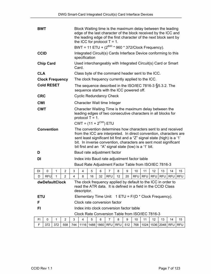
D Baud rate adjustment factor
DI Index into Baud rate adjustment factor table Baud Rate Adjustment Factor Table from ISO/IEC 7816-3
DI 0 1 2 3 4 5 6 7 8 9 10 11 12 13 14 15
D RFU 1 2 4 8 16 32 RFU 12 20 RFU RFU RFU RFU RFU RFU
dwDefaultClock The clock frequency applied by default to the ICC in order to read the ATR data. It is defined in a field in the CCID Class descriptor.
ETU Elementary Time Unit: 1 ETU = F/(D * Clock Frequency). F Clock rate conversion factor FI Index into clock conversion factor table
Clock Rate Conversion Table from ISO/IEC 7816-3 FI 0 1 2 3 4 5 6 7 8 9 10 11 12 13 14 15
F 372 372 558 744 1116 1488 1860 RFU RFU 512 768 1024 1536 2048 RFU RFU
CCID Rev 1.1 Page 7 of 123
DWG Smart-Card Integrated Circuit(s) Card Interface Devices
ICC Integrated Circuit(s) Cards Interface Device Terminal communication device or machine to which the ICC is
electrically connected during operation [ISO/IEC 7816-3]. IFSC Information Field Size for ICC for protocol T = 1. IFSD Information Field Size for CCID for protocol T = 1. INS Instruction byte of the command header sent to the ICC ISO/IEC International Standards Organization/ International Electro
technical Commission Lc Optional part of the body of a command APDU. Its size is 1, 2, or
3 bytes. The maximum number of bytes present in this body. Le Optional part of the body of a command APDU. Its size is 1, 2, or
3 bytes. The maximum number of bytes expected in the data field of the response APDU.
LRC Longitudinal Redundancy Check NAD Node Address P1, P2 INS parameter of a command header (T = 0 or APDU). P3 INS parameter of a T = 0 command header. The number of data
bytes to be transferred during the command. PPS Protocol and Parameter Selection RFU Reserved for Future Use – Must be set to zero unless stated
differently. Slot A physical connection with an ICC Smart Card Any of a number of similar devices conforming to
ISO/IEC 7816-3. T=0 Command Header
The sequence of five bytes; CLA INS P1 P2 P3 [ISO/IEC 7816-3 § 8.3.2].
TPDU Transport Protocol Data Unit USB-ICC USB Integrated Circuit(s) Card. An ICC providing a USB interface
[ISO/IEC 7816-12]. Warm RESET The sequence described in the [ISO/IEC 7816-3 § 5.3.3]. The
sequence starts with the ICC already powered. WI Waiting time Integer for protocol T = 0 WWT Work Waiting Time is the maximum time allowed between the
leading edge of a character sent by the ICC and the leading edge of the previous character sent either by the ICC or the interface device; WWT = 960 * WI * F / Clock Frequency
Page 8 of 123 CCID Rev 1.1

DWG Smart-Card Integrated Circuit(s) Card Interface Devices
1.3 Document Conventions Fields that are larger than a byte are stored in little endian. Little endian is a method of storing data that places the least significant byte of multiple-byte values at lower storage addresses. For example, a 16-bit integer stored in little endian format places the least significant byte at the lower address and the most significant byte at the next address. This specification uses the following typographic conventions:
Table 1.3-1 Typographic conventions
Example of convention Description
bValue
bcdName
wOther
……
Placeholder prefixes such as ‘b’, ‘bcd’, and ‘w’ are used to denote placeholder type. For example:
ab array of bytes
b bits or bytes dependent on context
bcd binary-coded decimal
bm bit map
w word (2 bytes)
dw double word (4 bytes)
CCID Rev 1.1 Page 9 of 123
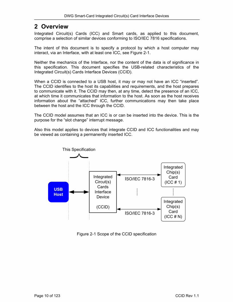
DWG Smart-Card Integrated Circuit(s) Card Interface Devices 2 Overview Integrated Circuit(s) Cards (ICC) and Smart cards, as applied to this document, comprise a selection of similar devices conforming to ISO/IEC 7816 specifications. The intent of this document is to specify a protocol by which a host computer may interact, via an Interface, with at least one ICC, see Figure 2-1. Neither the mechanics of the Interface, nor the content of the data is of significance in this specification. This document specifies the USB-related characteristics of the Integrated Circuit(s) Cards Interface Devices (CCID). When a CCID is connected to a USB host, it may or may not have an ICC “inserted”. The CCID identifies to the host its capabilities and requirements, and the host prepares to communicate with it. The CCID may then, at any time, detect the presence of an ICC, at which time it communicates that information to the host. As soon as the host receives information about the “attached” ICC, further communications may then take place between the host and the ICC through the CCID. The CCID model assumes that an ICC is or can be inserted into the device. This is the purpose for the “slot change” interrupt message. Also this model applies to devices that integrate CCID and ICC functionalities and may be viewed as containing a permanently inserted ICC.
This Specification
USBHost
IntegratedCircut(s)Cards
InterfaceDevice
(CCID)
ISO/IEC 7816-3
IntegratedChip(s)Card
(ICC # 1)
IntegratedChip(s)Card
(ICC # N)ISO/IEC 7816-3
Figure 2-1 Scope of the CCID specification
Page 10 of 123 CCID Rev 1.1
DWG Smart-Card Integrated Circuit(s) Card Interface Devices
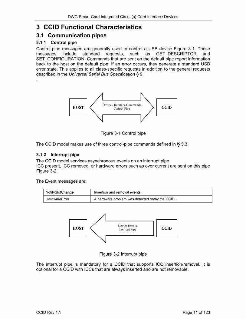
3 CCID Functional Characteristics 3.1 Communication pipes 3.1.1 Control pipe Control-pipe messages are generally used to control a USB device Figure 3-1. These messages include standard requests, such as GET_DESCRIPTOR and SET_CONFIGURATION. Commands that are sent on the default pipe report information back to the host on the default pipe. If an error occurs, they generate a standard USB error state. This applies to all class-specific requests in addition to the general requests described in the Universal Serial Bus Specification § 9. .
HOST CCIDDevice / Interface Commands
Control Pipe
Figure 3-1 Control pipe
The CCID model makes use of three control-pipe commands defined in § 5.3. 3.1.2 Interrupt pipe The CCID model services asynchronous events on an interrupt pipe. ICC present, ICC removed, or hardware errors such as over current are sent on this pipe Figure 3-2. The Event messages are:
NotifySlotChange Insertion and removal events.
HardwareError A hardware problem was detected on/by the CCID.
HOST CCIDDevice EventsInterrupt Pipe
Figure 3-2 Interrupt pipe
The interrupt pipe is mandatory for a CCID that supports ICC insertion/removal. It is optional for a CCID with ICCs that are always inserted and are not removable.
CCID Rev 1.1 Page 11 of 123

DWG Smart-Card Integrated Circuit(s) Card Interface Devices 3.1.3 Bulk-in, Bulk-out pipes CCID commands are sent on the BULK-OUT endpoint. Each command sent to the CCID has an associated ending response. Some commands can also have intermediate responses. The response is sent on the BULK-IN endpoint Figure 3-3.
HOST CCIDCCID Commands
Bulk Out Pipe
HOST
CCID
CCID Response Bulk In Pipe
HOST
CCID
CCID Response Bulk In Pipe
Figure 3-3 Bulk-in Bulk-out pipes
All commands, sent to the specific CCID slot, have to be sent synchronously. A specific slot can accept only one command at a time. A slot is considered to be idle if it is ready to receive a new command.
The Host can send up to bMaxCCIDBusySlots number of commands to the CCID if all of these commands are dedicated to different idle slots. It is the responsibility of the Host to keep track of all busy slots and to not exceed bMaxCCIDBusySlots number of active commands (busy slots).
When the number of active slots is equal to bMaxCCIDBusySlots, the CCID shall only accept general requests or the class-specific request to ABORT a slot over the control pipe.
When the CCID successfully receives a new command to a busy slot (not idle), it must fail this command by issuing a CMD_SLOT_BUSY error. To maintain track of all the commands, the Host sets a unique command identifier bSeq for each command sent to the CCID. To mark command completion the CCID sends the response with the same bSeq number. The driver will not send a new command to a slot until the ending response to the last command to that slot is received. If it is determined that the current command has erred or timed out, the response can be abandoned/aborted by issuing the class specific abandon/abort command to the control endpoint.
More than one BULK-IN message can be sent for each BULK-OUT message. For example, the CCID can send a BULK-IN message with a Time Extension status to notify
Page 12 of 123 CCID Rev 1.1
DWG Smart-Card Integrated Circuit(s) Card Interface Devices the host that the ICC has requested more time to process the ICC command and, after a delay, follow this with a second BULK-IN message with the ICC’s response to the command. When this happens, both BULK-IN messages have the same bSeq value.
The CCID is required to send a Zero Length Packet (ZLP) following any Bulk-In message that is a multiple of MaxPacketSize. This ZLP allows the CCID device driver to be more efficient, and is generally considered “good-practice” for USB bulk-in pipes. 3.2 Protocol and parameters selection A CCID announces in dwFeatures Table 5.1-1 one level of exchanges with the host, TPDU, APDU (Short and Extended), or Character. 3.2.1 TPDU level of exchange For TPDU level exchanges, the CCID provides the transportation of host’s TPDU to the ICC’s TPDU. The TPDU format changes according to the protocol or for PPS exchange. TPDU for PPS exchange has the following format: Command TPDU: FF PPS0 PPS1 PPS2 PPS3 PCK, with PPS1, PPS2, PPS3 optional [ISO/IEC7816-3 §7]. Response TPDU: FF PPS0_R PPS1_R PPS2_R PPS3_R PCK_R, with PPS1_R, PPS2_R, PPS3_R optional [ISO/IEC7816-3 §7.4). The CCID implements and verifies timings and protocol according to its parameters settings to assume ISO/IEC 7816-3 §7.1, §7.2. No check on frame format is mandatory on request, and on response the only recommended analysis is the most significant nibble of PPS0_R to compute the number of bytes left to receive. A CCID that implements automatic PPS should not accept TPDU for PPS exchange and must check for PPS response validity.
T = 0 TPDU can have three formats [ISO/IEC 7816-3, § 8.3.2]:
- Form 1, no data to exchange with ICC, only header: Command TPDU = CLA INS P1 P2, the CCID is responsible to add P3=00h. Response TPDU = SW1 SW2 - Form 2, data expected from ICC: Command TPDU = CLA INS P1 P2 Le, Le=P3 from 00h to FFh (00h means 100h) Response TPDU = Data(Le) SW1 SW2, Data(Le) is for the Le data received from the ICC or empty if ICC rejects the command. - Form 3, data are to be sent to the ICC: Command TPDU = CLA INS P1 P2 Lc Data(Lc), Lc=P3 from 01h to FFh and Data(Lc) for the Lc data to send to the ICC. Response TPDU = SW1 SW2 The CCID, for T=0 TPDU, is in charge of managing procedure bytes (ISO 7816-3 § 8.3.3) and character level [ISO]IEC 7816-3 § 8.2]. The procedure bytes are not mapped into the response TPDU except for the SW1 SW2 bytes. The CCID implements and verifies timings according to its
CCID Rev 1.1 Page 13 of 123
DWG Smart-Card Integrated Circuit(s) Card Interface Devices
parameters settings to assume ISO/IEC 7816-3 § 8.2 (work waiting time, extra guard time, …). If ICC uses NULL procedure byte (60h) the CCID informs the host of this request for time extension.
T = 1 TPDU command and response use the frame format [ISO/IEC 7816-3 § 9.4]. The CCID expects the respect of the character frame [ISO/IEC 7816-3 § 9.4.1]. But no check on frame format is mandatory on sending, and on receiving. The only recommended checks are:
- Expecting LEN byte as third byte - Wait for LEN bytes as INF field. - Wait for an EDC field which length complies with parameter bmTCCKST1 (see § 6.1.7).
The CCID implements and verifies timing according to its parameters settings to assume ISO/IEC 7816-3 § 9.5.3 (CWT, BWT, BGT, …). The detection of parity error on character received is optional. The interpretation of first bytes received as NAD and PCB to manage VPP is optional and depends on CCID capabilities. 3.2.2 APDU level of exchange For APDU level exchanges, the CCID provides the transportation of host’s APDU to ICC’s TPDU. APDU commands and responses are defined in ISO 7816-4. Two APDU levels are defined, short APDU and extended APDU. Short APDU and extended APDU are defined in ISO/IEC 7816-4 § 5.3.2.
A CCID that indicates a short APDU exchange only accepts short APDU. A CCID that indicates an extended APDU exchange accepts both short APDU and extended APDU.
If the ICC requests time extension, by using a NULL procedure byte (60h) in T=0 protocol or S(WTX) in T=1 protocol, the CCID informs the host of this request.
A CCID supporting APDU level of exchanges implements a high level of automatism in ICC communications. It shall also provide a high level of automatism in ATR treatment and implement one of the following automatisms: automatic parameters negotiation (proprietary algorithm), or automatic PPS according to the current parameters. At least two standards of transportation for APDU are defined, ISO/IEC 7816-4 and EMV 3.1.1, which standard to implement is out of the scope of this specification. 3.2.3 Character level of exchange Character level of exchanges is selected when none of the TPDU, Short APDU or Short and extended APDU is selected. The CCID sends the characters in the command (maybe none) then waits for the number of characters (if not null) indicated in the command. For character level exchange between the host and the CCID, the CCID supports asynchronous characters communication with the ICC as per ISO 7816-3 § 6.3 including
Page 14 of 123 CCID Rev 1.1
DWG Smart-Card Integrated Circuit(s) Card Interface Devices timings defined in ISO/IEC 7816-3 § 8.2 for T = 0 and in ISO 7816-3 § 9.3 for T = 1. To respect timing the CCID shall use the defined parameters. The CCID implements the character frame and character repetition procedure when T = 0 is selected.
3.3 Suspend Behavior When resuming from a USB suspend, the host/driver will assume that all ICCs have been deactivated (powered down). When the USB bus suspends, CCIDs are not required to deactivate inserted ICCs, but may do so; however, after the USB bus resumes, CCIDs must respond to the host as if all of the inserted ICCs had been deactivated and newly inserted. After resuming, the CCID will do two things in no particular order. 1. Send the RDR_to_PC_NotifySlotChange message to inform the driver which slots
have “newly inserted" cards. 2. The CCID will reactivate the ICCs only from a PC_to_RDR_IccPowerOn message
from the driver or automatically if the CCID has the "automatic activation on insertion" feature. Note: When reactivating, all slot parameters initially revert back to the defaults.
CCID Rev 1.1 Page 15 of 123
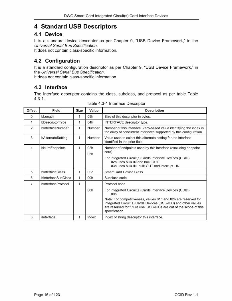
DWG Smart-Card Integrated Circuit(s) Card Interface Devices 4 Standard USB Descriptors 4.1 Device It is a standard device descriptor as per Chapter 9, “USB Device Framework,” in the Universal Serial Bus Specification. It does not contain class-specific information. 4.2 Configuration It is a standard configuration descriptor as per Chapter 9, “USB Device Framework,” in the Universal Serial Bus Specification. It does not contain class-specific information. 4.3 Interface The Interface descriptor contains the class, subclass, and protocol as per table Table 4.3-1.
Table 4.3-1 Interface Descriptor Offset Field Size Value Description
0 bLength 1 09h Size of this descriptor in bytes.
1 bDescriptorType 1 04h INTERFACE descriptor type.
2 bInterfaceNumber 1 Number Number of this interface. Zero-based value identifying the index in the array of concurrent interfaces supported by this configuration.
3 bAlternateSetting 1 Number Value used to select this alternate setting for the interface identified in the prior field.
4 bNumEndpoints 1 02h
03h
Number of endpoints used by this interface (excluding endpoint zero).
For Integrated Circuit(s) Cards Interface Devices (CCID) 02h uses bulk-IN and bulk-OUT 03h uses bulk-IN, bulk-OUT and interrupt –IN
5 bInterfaceClass 1 0Bh Smart Card Device Class.
6 bInterfaceSubClass 1 00h Subclass code.
7 bInterfaceProtocol 1
00h
Protocol code
For Integrated Circuit(s) Cards Interface Devices (CCID) 00h
Note: For competitiveness, values 01h and 02h are reserved for Integrated Circuit(s) Cards Devices (USB-ICC) and other values are reserved for future use. USB-ICCs are out of the scope of this specification.
8 iInterface 1 Index Index of string descriptor this interface.
Page 16 of 123 CCID Rev 1.1

DWG Smart-Card Integrated Circuit(s) Card Interface Devices
5 Smart Card Device Class 5.1 Descriptor The Smart Card Device Class Descriptor Table 5.1-1 specifies certain device features or capabilities selected as per § 3.2.
Table 5.1-1 Smart Card Device Class Descriptors
Offset Field Size Value Description
0 bLength 1 36h Size of this descriptor, in bytes.
1 bDescriptorType 1 21h Functional Descriptor type.
2 bcdCCID 2 0110h Integrated Circuit(s) Cards Interface Devices (CCID) Specification Release Number in Binary-Coded decimal (i.e., 2.10 is 0210h).
4 bMaxSlotIndex 1 The index of the highest available slot on this device. All slots are consecutive starting at 00h.
i.e. 0Fh = 16 slots on this device numbered 00h to 0Fh.
5 bVoltageSupport 1 This value indicates what voltages the CCID can supply to its slots. It is a bitwise OR operation performed on the following values:
• 01h 5.0V • 02h 3.0V • 04h 1.8V
Other bits are RFU.
6 dwProtocols 4 RRRR
PPPP
RRRR –Upper Word- is RFU = 0000h
PPPP –Lower Word- Encodes the supported protocol types. A ‘1’ in a given bit position indicates support for the associated ISO protocol. 0001h = Protocol T=0 0002h = Protocol T=1 All other bits are reserved and must be set to zero. The field is intended to correspond to the PCSC specification definitions. See PCSC Part3. Table 3-1 Tag 0x0120.
Example: 00000003h indicates support for T = 0 and T = 1.
10 dwDefaultClock 4 Default ICC clock frequency in KHz. This is an integer value.
Example: 3.58 MHz is encoded as the integer value 3580. (00000DFCh)
This is used in ETU and waiting time calculations. It is the clock frequency used when reading the ATR data.
14 dwMaximumClock 4 Maximum supported ICC clock frequency in KHz. This is an integer value.
Example: 14.32 MHz is encoded as the integer value 14320. (000037F0h)
CCID Rev 1.1 Page 17 of 123
DWG Smart-Card Integrated Circuit(s) Card Interface Devices
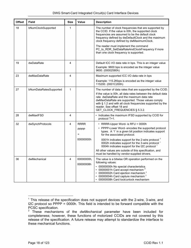
Offset Field Size Value Description
18 bNumClockSupported 1 The number of clock frequencies that are supported by the CCID. If the value is 00h, the supported clock frequencies are assumed to be the default clock frequency defined by dwDefaultClock and the maximum clock frequency defined by dwMaximumClock.
The reader must implement the command PC_to_RDR_SetDataRateAndClockFrequency if more than one clock frequency is supported.
19 dwDataRate 4 Default ICC I/O data rate in bps. This is an integer value Example: 9600 bps is encoded as the integer value 9600. (00002580h)
23 dwMaxDataRate 4 Maximum supported ICC I/O data rate in bps
Example: 115.2Kbps is encoded as the integer value 115200. (0001C200h)
27 bNumDataRatesSupported 1 The number of data rates that are supported by the CCID. If the value is 00h, all data rates between the default data rate dwDataRate and the maximum data rate dwMaxDataRate are supported. Those values comply with § 1.2 and with all clock frequencies supported by the reader. See offset 18 and GET_CLOCK_FREQUENCIES § 5.3.2.
28 dwMaxIFSD 4 • Indicates the maximum IFSD supported by CCID for protocol T=1.
32 dwSynchProtocols 4 RRRR
PPPP
=
00000000h
• RRRR-Upper Word- is RFU = 0000h • PPPP-Lower Word- encodes the supported protocol
types. A ‘1’ in a given bit position indicates support for the associated protocol.
0001h indicates support for the 2-wire protocol 1 0002h indicates support for the 3-wire protocol 1 0004h indicates support for the I2C protocol 1
All other values are outside of this specification, and must be handled by vendor-supplied drivers.
36 dwMechanical 4 00000000h,
00000008h
The value is a bitwise OR operation performed on the following values: • 00000000h No special characteristics • 00000001h Card accept mechanism 2 • 00000002h Card ejection mechanism 2 • 00000004h Card capture mechanism 2 • 00000008h Card lock/unlock mechanism
1 This release of the specification does not support devices with the 2-wire, 3-wire, and I2C protocol so PPPP = 0000h. This field is intended to be forward compatible with the PCSC specification. 2 These mechanisms of the dwMechanical parameter have been included for completeness; however, these functions of motorized CCIDs are not covered by this release of the specification. A future release may attempt to standardize the interface to these mechanical functions.
Page 18 of 123 CCID Rev 1.1

DWG Smart-Card Integrated Circuit(s) Card Interface Devices
Offset Field Size Value Description
40 dwFeatures 4 xxxxxxxxh This value indicates what intelligent features the CCID has. The value is a bitwise OR operation performed on the following values:
• 00000000h No special characteristics
• 00000002h Automatic parameter configuration based on ATR data
• 00000004h Automatic activation of ICC on inserting
• 00000008h Automatic ICC voltage selection • 00000010h Automatic ICC clock frequency change according to active parameters provided by the Host or self
determined 3
• 00000020h 3 Automatic baud rate change according to active parameters provided by the Host or self determined
• 00000040h 4 Automatic parameters negotiation made by the CCID (use of warm or cold resets or PPS according to a manufacturer proprietary algorithm to select the communication parameters with the ICC)
• 00000080h 4 Automatic PPS made by the CCID according to the active parameters
• 00000100h CCID can set ICC in clock stop mode
• 00000200h NAD value other than 00 accepted (T=1 protocol in use)
• 00000400h Automatic IFSD exchange as first exchange (T=1 protocol in use)
Only one of the following values may be present to select a level of exhange: • 00010000h TPDU level exchanges with CCID • 00020000h Short APDU level exchange with CCID • 00040000h Short and Extended APDU level exchange with CCID • If none of those values is indicated the level of exchange is
character. Only one of the values 00000040h and 00000080h may be present. When value 00000040h is present the host shall not try to change the FI, DI, and protocol currently selected.
When an APDU level for exchanges is selected, one of the values 00000040h or 00000080h must be present, as well as the value 00000002h.
To support selective suspend: • 00100000h USB Wake up signaling supported on card insertion
and removal
When bit 20th, as shown above, is set bit D5 in bmAttributes of the Standard Configuration Descriptor must be set to 1.
3 When a CCID doesn't declare the value 00000010h the frequency must be made via the manufacturer proprietary PC_to_RDR_Escape command, same thing for the baud rate when the value 00000020h is not declared. 4 When a CCID using TPDU exchange level declares neither of the values 00000040h, or 00000080h, the PPS exchange must be made using a TPDU for PPS exchange.
CCID Rev 1.1 Page 19 of 123
DWG Smart-Card Integrated Circuit(s) Card Interface Devices
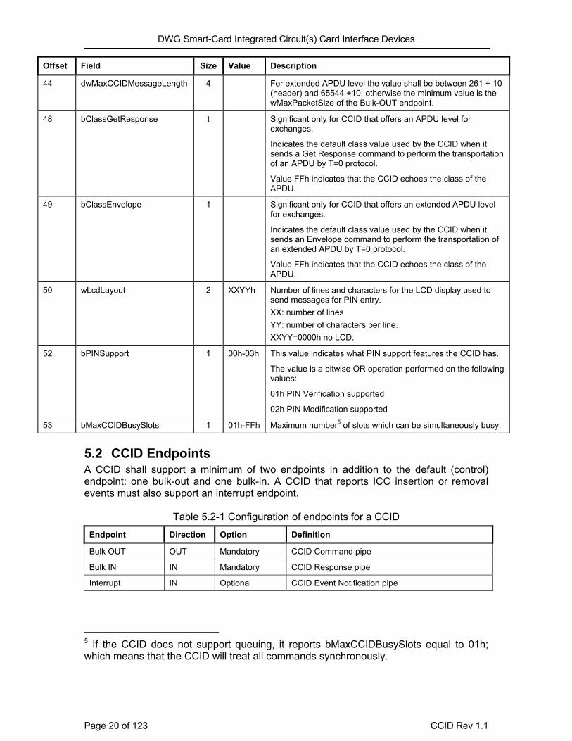
Offset Field Size Value Description
44 dwMaxCCIDMessageLength 4 For extended APDU level the value shall be between 261 + 10 (header) and 65544 +10, otherwise the minimum value is the wMaxPacketSize of the Bulk-OUT endpoint.
48 bClassGetResponse 1 Significant only for CCID that offers an APDU level for exchanges.
Indicates the default class value used by the CCID when it sends a Get Response command to perform the transportation of an APDU by T=0 protocol.
Value FFh indicates that the CCID echoes the class of the APDU.
49 bClassEnvelope 1 Significant only for CCID that offers an extended APDU level for exchanges.
Indicates the default class value used by the CCID when it sends an Envelope command to perform the transportation of an extended APDU by T=0 protocol.
Value FFh indicates that the CCID echoes the class of the APDU.
50 wLcdLayout 2 XXYYh Number of lines and characters for the LCD display used to send messages for PIN entry. XX: number of lines YY: number of characters per line. XXYY=0000h no LCD.
52 bPINSupport 1 00h-03h This value indicates what PIN support features the CCID has.
The value is a bitwise OR operation performed on the following values:
01h PIN Verification supported
02h PIN Modification supported
53 bMaxCCIDBusySlots 1 01h-FFh Maximum number5 of slots which can be simultaneously busy.
5.2 CCID Endpoints A CCID shall support a minimum of two endpoints in addition to the default (control) endpoint: one bulk-out and one bulk-in. A CCID that reports ICC insertion or removal events must also support an interrupt endpoint.
Table 5.2-1 Configuration of endpoints for a CCID
Endpoint Direction Option Definition
Bulk OUT OUT Mandatory CCID Command pipe
Bulk IN IN Mandatory CCID Response pipe
Interrupt IN Optional CCID Event Notification pipe
5 If the CCID does not support queuing, it reports bMaxCCIDBusySlots equal to 01h; which means that the CCID will treat all commands synchronously.
Page 20 of 123 CCID Rev 1.1

DWG Smart-Card Integrated Circuit(s) Card Interface Devices 5.2.1 Bulk-OUT Endpoint The Bulk Out Endpoint is used to send commands and transfer data from the host to the device.
Offset Field Size Value Description
0 bLength 1 07h Size of this descriptor in bytes
1 bDescriptorType 1 05h ENDPOINT descriptor type
2 bEndpointAddress 1 01-0Fh The address of this endpoint on the USB device. This address is an endpoint number between 1 and 15.
Bit 0..3 Endpoint number
Bit 4..6 Reserved, must be 0
Bit 7 0 = Out
3 bmAttributes 1 02h This is a Bulk endpoint
4 wMaxPacketSize 2 0xyzh Maximum data transfer size can be 8, 16, 32, 64, or 512 bytes
6 bInterval 1 Number For Full Speed: Ignored For High-Speed: The bInterval must specify the maximum NAK rate of the endpoint. A value of 0 indicates the endpoint never NAKs. Other values indicate at most 1 NAK each bInterval number of microframes. This value must be in the range from 0 to 255.
5.2.2 Bulk-IN Endpoint The Bulk In endpoint is used to send responses and transfer data from the device to the host in reply to commands received on the Command Pipe.
Offset Field Size Value Description
0 bLength 1 07h Size of this descriptor in bytes
1 bDescriptorType 1 05h ENDPOINT descriptor type
2 bEndpointAddress 1 81-8Fh The address of this endpoint on the USB device. This address is an endpoint number between 1 and 15.
Bit 0..3 Endpoint number
Bit 4..6 Reserved, must be 0
Bit 7 1 = In
3 bmAttributes 1 02h This is a Bulk endpoint
4 wMaxPacketSize 2 0xyzh Maximum data transfer size can be 8, 16, 32, 64 or 512 bytes
6 bInterval 1 Number For Full Speed: Ignored For High Speed: Interval for polling endpoint for data transfers. Expressed in frames or microframes depending on the device operating speed (i.e., either 1 millisecond or 125 µs units).
CCID Rev 1.1 Page 21 of 123
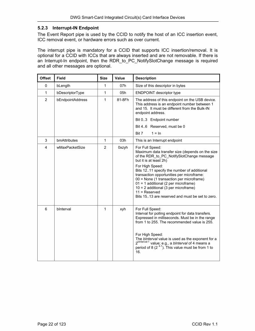
DWG Smart-Card Integrated Circuit(s) Card Interface Devices 5.2.3 Interrupt-IN Endpoint The Event Report pipe is used by the CCID to notify the host of an ICC insertion event, ICC removal event, or hardware errors such as over current. The interrupt pipe is mandatory for a CCID that supports ICC insertion/removal. It is optional for a CCID with ICCs that are always inserted and are not removable. If there is an Interrupt-In endpoint, then the RDR_to_PC_NotifySlotChange message is required and all other messages are optional.
Offset Field Size Value Description
0 bLength 1 07h Size of this descriptor in bytes
1 bDescriptorType 1 05h ENDPOINT descriptor type
2 bEndpointAddress 1 81-8Fh The address of this endpoint on the USB device. This address is an endpoint number between 1 and 15. It must be different from the Bulk-IN endpoint address.
Bit 0..3 Endpoint number
Bit 4..6 Reserved, must be 0
Bit 7 1 = In
3 bmAttributes 1 03h This is an Interrupt endpoint
4 wMaxPacketSize 2 0xzyh For Full Speed: Maximum data transfer size (depends on the size of the RDR_to_PC_NotifySlotChange message but it is at least 2h) For High Speed: Bits 12..11 specify the number of additional transaction opportunities per microframe: 00 = None (1 transaction per microframe) 01 = 1 additional (2 per microframe) 10 = 2 additional (3 per microframe) 11 = Reserved Bits 15..13 are reserved and must be set to zero.
6 bInterval 1 xyh For Full Speed: Interval for polling endpoint for data transfers. Expressed in milliseconds. Must be in the range from 1 to 255. The recommended value is 255.
For High Speed: The bInterval value is used as the exponent for a 2bInterval-1 value; e.g., a bInterval of 4 means a period of 8 (2 4-1). This value must be from 1 to 16.
Page 22 of 123 CCID Rev 1.1
DWG Smart-Card Integrated Circuit(s) Card Interface Devices
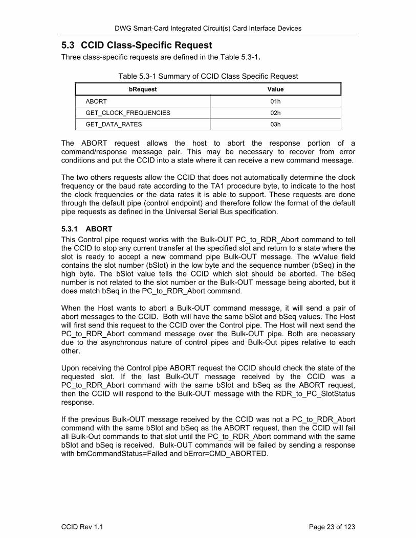
5.3 CCID Class-Specific Request Three class-specific requests are defined in the Table 5.3-1.
Table 5.3-1 Summary of CCID Class Specific Request
bRequest Value
ABORT 01h
GET_CLOCK_FREQUENCIES 02h
GET_DATA_RATES 03h
The ABORT request allows the host to abort the response portion of a command/response message pair. This may be necessary to recover from error conditions and put the CCID into a state where it can receive a new command message. The two others requests allow the CCID that does not automatically determine the clock frequency or the baud rate according to the TA1 procedure byte, to indicate to the host the clock frequencies or the data rates it is able to support. These requests are done through the default pipe (control endpoint) and therefore follow the format of the default pipe requests as defined in the Universal Serial Bus specification. 5.3.1 ABORT This Control pipe request works with the Bulk-OUT PC_to_RDR_Abort command to tell the CCID to stop any current transfer at the specified slot and return to a state where the slot is ready to accept a new command pipe Bulk-OUT message. The wValue field contains the slot number (bSlot) in the low byte and the sequence number (bSeq) in the high byte. The bSlot value tells the CCID which slot should be aborted. The bSeq number is not related to the slot number or the Bulk-OUT message being aborted, but it does match bSeq in the PC_to_RDR_Abort command. When the Host wants to abort a Bulk-OUT command message, it will send a pair of abort messages to the CCID. Both will have the same bSlot and bSeq values. The Host will first send this request to the CCID over the Control pipe. The Host will next send the PC_to_RDR_Abort command message over the Bulk-OUT pipe. Both are necessary due to the asynchronous nature of control pipes and Bulk-Out pipes relative to each other. Upon receiving the Control pipe ABORT request the CCID should check the state of the requested slot. If the last Bulk-OUT message received by the CCID was a PC_to_RDR_Abort command with the same bSlot and bSeq as the ABORT request, then the CCID will respond to the Bulk-OUT message with the RDR_to_PC_SlotStatus response. If the previous Bulk-OUT message received by the CCID was not a PC_to_RDR_Abort command with the same bSlot and bSeq as the ABORT request, then the CCID will fail all Bulk-Out commands to that slot until the PC_to_RDR_Abort command with the same bSlot and bSeq is received. Bulk-OUT commands will be failed by sending a response with bmCommandStatus=Failed and bError=CMD_ABORTED.
CCID Rev 1.1 Page 23 of 123
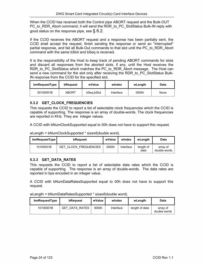
DWG Smart-Card Integrated Circuit(s) Card Interface Devices When the CCID has received both the Control pipe ABORT request and the Bulk-OUT PC_to_RDR_Abort command, it will send the RDR_to_PC_SlotStatus Bulk-IN reply with good status on the response pipe, see § 6.2. If the CCID receives the ABORT request and a response has been partially sent, the CCID shall accept the request, finish sending the response or send an "interrupted" partial response, and fail all Bulk-Out commands to that slot until the PC_to_RDR_Abort command with the same bSlot and bSeq is received. It is the responsibility of the Host to keep track of pending ABORT commands for slots and discard all responses from the aborted slots, if any, until the Host receives the RDR_to_PC_SlotStatus which matches the PC_to_RDR_Abort message. The Host can send a new command for the slot only after receiving the RDR_to_PC_SlotStatus Bulk-IN response from the CCID for the specified slot.
bmRequestType bRequest wValue wIndex wLength Data
00100001B ABORT bSeq,bSlot Interface 0000h None
5.3.2 GET_CLOCK_FREQUENCIES This requests the CCID to report a list of selectable clock frequencies which the CCID is capable of supporting. The response is an array of double-words. The clock frequencies are reported in KHz. They are integer values. A CCID with bNumClockSupported equal to 00h does not have to support this request. wLength = bNumClockSupported * sizeof(double word).
bmRequestType bRequest wValue wIndex wLength Data
10100001B GET_CLOCK_FREQUENCIES 0000h Interface length of data
array of double words
5.3.3 GET_DATA_RATES This requests the CCID to report a list of selectable data rates which the CCID is capable of supporting. The response is an array of double-words. The data rates are reported in bps encoded in an integer value. A CCID with bNumDataRatesSupported equal to 00h does not have to support this request. wLength = bNumDataRatesSupported * sizeof(double word).
bmRequestType bRequest wValue wIndex wLength Data
10100001B GET_DATA_RATES 0000h Interface length of data array of double words
Page 24 of 123 CCID Rev 1.1
DWG Smart-Card Integrated Circuit(s) Card Interface Devices
6 CCID Messages All bulk messages begin with a 10-bytes header, followed by message-specific data. The header consists of a message type (1 byte), a length field (four bytes), the slot number (1 byte), a sequence number field (1 byte), and either three message specific bytes, or a status field (1 byte), an error field and one message specific byte. The purpose of the 10-byte header is to provide a constant offset at which message data begins across all messages. A Bulk-OUT message is a command, and always receives at least one Bulk-IN message in response. The response messages always contain the exact same slot number, and sequence number fields from the header that was contained in the Bulk-OUT command message. The message type (bMessageType) identifies the message. The length field (dwLength) is the length of the message not including the 10-byte header. The slot number (bSlot) identifies which ICC slot is being addressed by the message, if the CCID supports multiple slots. The slot number is zero-relative, and is in the range of zero to FFh. The sequence number (bSeq) is a monotonically increasing by one counter of bulk messages sent to the CCID. Because the response to a command always uses the exact same sequence number contained in the command, the host can use the sequence number in a response message to verify that a particular response is the one expected in reply to a particular command. This sequence number is not related to any interaction between the CCID and the ICC itself, but simply tracks the USB bulk message exchanges between the host and the CCID. The initial value of the sequence number is not important, but typically starts at zero. Slot Status (bStatus) is returned in the Bulk-IN message response, see § 6.2.6. Slot Error (bError) is returned in the Bulk-IN message response, see § 6.2.6. The remaining bytes of the header (3 bytes in Bulk-OUT messages and 1 byte in Bulk-IN message) are message specific.
CCID Rev 1.1 Page 25 of 123
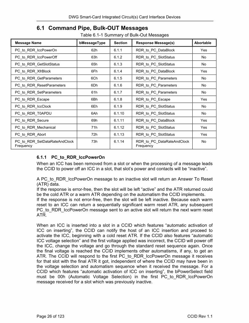
DWG Smart-Card Integrated Circuit(s) Card Interface Devices 6.1 Command Pipe, Bulk-OUT Messages
Table 6.1-1 Summary of Bulk-Out Messages
Message Name bMessageType Section Response Message(s) Abortable
PC_to_RDR_IccPowerOn 62h 6.1.1 RDR_to_PC_DataBlock Yes
PC_to_RDR_IccPowerOff 63h 6.1.2 RDR_to_PC_SlotStatus No
PC_to_RDR_GetSlotStatus 65h 6.1.3 RDR_to_PC_SlotStatus No
PC_to_RDR_XfrBlock 6Fh 6.1.4 RDR_to_PC_DataBlock Yes
PC_to_RDR_GetParameters 6Ch 6.1.5 RDR_to_PC_Parameters No
PC_to_RDR_ResetParameters 6Dh 6.1.6 RDR_to_PC_Parameters No
PC_to_RDR_SetParameters 61h 6.1.7 RDR_to_PC_Parameters No
PC_to_RDR_Escape 6Bh 6.1.8 RDR_to_PC_Escape Yes
PC_to_RDR_IccClock 6Eh 6.1.9 RDR_to_PC_SlotStatus No
PC_to_RDR_T0APDU 6Ah 6.1.10 RDR_to_PC_SlotStatus No
PC_to_RDR_Secure 69h 6.1.11 RDR_to_PC_DataBlock Yes
PC_to_RDR_Mechanical 71h 6.1.12 RDR_to_PC_SlotStatus Yes
PC_to_RDR_Abort 72h 6.1.13 RDR_to_PC_SlotStatus Yes
PC_to_RDR_SetDataRateAndClockFrequency
73h 6.1.14 RDR_to_PC_DataRateAndClockFrequency
No
6.1.1 PC_to_RDR_IccPowerOn When an ICC has been removed from a slot or when the processing of a message leads the CCID to power off an ICC in a slot, that slot’s power and contacts will be “inactive”. A PC_to_RDR_IccPowerOn message to an inactive slot will return an Answer To Reset (ATR) data. If the response is error-free, then the slot will be left “active” and the ATR returned could be the cold ATR or a warm ATR depending on the automatism the CCID implements. If the response is not error-free, then the slot will be left inactive. Because each warm reset to an ICC can return a sequentially significant warm reset ATR, any subsequent PC_to_RDR_IccPowerOn message sent to an active slot will return the next warm reset ATR. When an ICC is inserted into a slot in a CCID which features “automatic activation of ICC on inserting”, the CCID can notify the host of an ICC insertion and proceed to activate the ICC, beginning with a cold reset ATR. If the CCID also features “automatic ICC voltage selection” and the first voltage applied was incorrect, the CCID will power off the ICC, change the voltage and go through the standard reset sequence again. Once the final voltage is reached the CCID implements other automatisms, if any, to get an ATR. The CCID will respond to the first PC_to_RDR_IccPowerOn message it receives for that slot with the final ATR it got, independent of where the CCID may have been in the voltage selection and automatism sequence when it received the message. For a CCID which features “automatic activation of ICC on inserting”, the bPowerSelect field must be 00h (Automatic Voltage Selection) in the first PC_to_RDR_IccPowerOn message received for a slot which was previously inactive.
Page 26 of 123 CCID Rev 1.1
DWG Smart-Card Integrated Circuit(s) Card Interface Devices A CCID which does not feature “automatic activation of ICC on inserting”, will notify the host of an ICC insertion and wait, with its contacts inactive, for the PC_to_RDR_IccPowerOn message before doing the standard reset sequence at the voltage specified by the bPowerSelect field. If the CCID features “automatic ICC voltage selection” and the first PC_to_RDR_IccPowerOn message selects automatic voltage selection in the bPowerSelect field, the CCID will return an ATR of the final voltage. To change the voltage on a slot that is active, the slot must first be powered off before issuing a PC_to_RDR_IccPowerOn message with a new bPowerSelect value. For reference, ISO/IEC 7816-3:1997 § 4.2.2 requires that the power must be off for at least 10 milliseconds. On reception of a PC_to_RDR_IccPowerOn command, the CCID automatically resets the parameters to their default values except for the following case. If the CCID has the "automatic activation of ICC on inserting" feature, and the PC_to_RDR_IccPowerOn command is the first PC_to_RDR_IccPowerOn command the CCID has received since either 1) the ICC was first inserted into the slot or 2) the CCID has resumed from the suspended state, then the CCID will not reset the parameters because the CCID already reset them before it started the automatic activation sequence. The "automatic activation" CCID keeps the parameters it read and negotiated during the automatic activation sequence. On reception of any subsequent PC_to_RDR_IccPowerOn commands, the "automatic activation" CCID automatically resets the parameters to their default values.
Offset Field Size Value Description
0 bMessageType 1 62h
1 dwLength 4 00000000h Message-specific data length
5 bSlot 1 00-FFh Identifies the slot number for this command
6 bSeq 1 00-FFh Sequence number for command.
7 bPowerSelect 1 00h, 01h, 02h, or 03h
Voltage that is applied to the ICC
00h – Automatic Voltage Selection
01h – 5.0 volts
02h – 3.0 volts
03h – 1.8 volts
8 abRFU 2 Reserved for Future Use
CCID Rev 1.1 Page 27 of 123
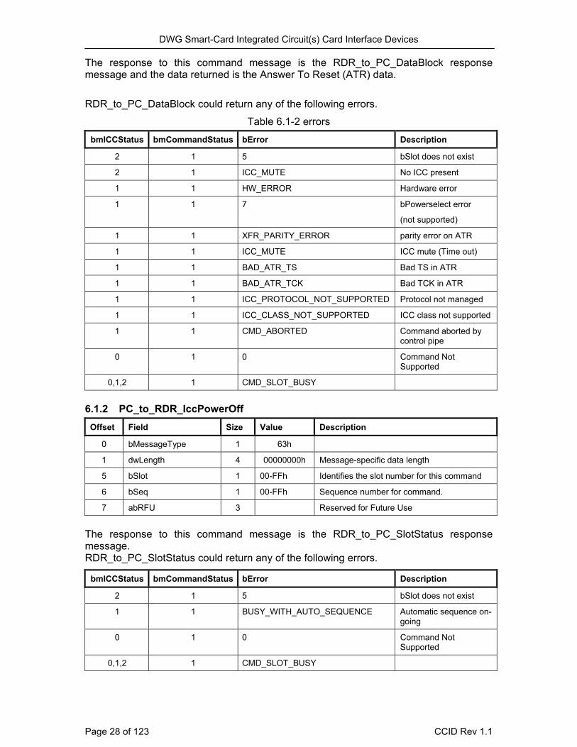
DWG Smart-Card Integrated Circuit(s) Card Interface Devices The response to this command message is the RDR_to_PC_DataBlock response message and the data returned is the Answer To Reset (ATR) data.
RDR_to_PC_DataBlock could return any of the following errors.
Table 6.1-2 errors
bmICCStatus bmCommandStatus bError Description
2 1 5 bSlot does not exist
2 1 ICC_MUTE No ICC present
1 1 HW_ERROR Hardware error
1 1 7 bPowerselect error
(not supported)
1 1 XFR_PARITY_ERROR parity error on ATR
1 1 ICC_MUTE ICC mute (Time out)
1 1 BAD_ATR_TS Bad TS in ATR
1 1 BAD_ATR_TCK Bad TCK in ATR
1 1 ICC_PROTOCOL_NOT_SUPPORTED Protocol not managed
1 1 ICC_CLASS_NOT_SUPPORTED ICC class not supported
1 1 CMD_ABORTED Command aborted by control pipe
0 1 0 Command Not Supported
0,1,2 1 CMD_SLOT_BUSY
6.1.2 PC_to_RDR_IccPowerOff
Offset Field Size Value Description
0 bMessageType 1 63h
1 dwLength 4 00000000h Message-specific data length
5 bSlot 1 00-FFh Identifies the slot number for this command
6 bSeq 1 00-FFh Sequence number for command.
7 abRFU 3 Reserved for Future Use
The response to this command message is the RDR_to_PC_SlotStatus response message. RDR_to_PC_SlotStatus could return any of the following errors.
bmICCStatus bmCommandStatus bError Description
2 1 5 bSlot does not exist
1 1 BUSY_WITH_AUTO_SEQUENCE Automatic sequence on-going
0 1 0 Command Not Supported
0,1,2 1 CMD_SLOT_BUSY
Page 28 of 123 CCID Rev 1.1
DWG Smart-Card Integrated Circuit(s) Card Interface Devices 6.1.3 PC_to_RDR_GetSlotStatus
Offset Field Size Value Description
0 bMessageType 1 65h
1 dwLength 4 00000000h Message-specific data length
5 bSlot 1 00-FFh Identifies the slot number for this command
6 bSeq 1 00-FFh Sequence number for command.
7 abRFU 3 Reserved for Future Use
The response to this command message is the RDR_to_PC_SlotStatus response message. RDR_to_PC_SlotStatus could return any of the following errors.
bmICCStatus bmCommandStatus bError Description
2 1 5 bSlot does not exist
2 1 ICC_MUTE No ICC present
1 1 HW_ERROR Hardware error
0 1 0 Command Not Supported
0,1,2 1 CMD_SLOT_BUSY
CCID Rev 1.1 Page 29 of 123
DWG Smart-Card Integrated Circuit(s) Card Interface Devices 6.1.4 PC_to_RDR_XfrBlock The block should never exceed the dwMaxCCIDMessageLength-10 in the Class Descriptor. Parameter bBWI is only used by CCIDs which use the character level and TPDU level of exchange (as reported in the dwFeatures parameter in the CCID Functional Descriptor) and only for protocol T=1 transfers.
Offset Field Size Value Description
0 bMessageType 1 6Fh
1 dwLength 4 Size of abData field of this message
5 bSlot 1 00-FFh Identifies the slot number for this command
6 bSeq 1 00-FFh Sequence number for command.
7 bBWI 1 00-FFh Used to extend the CCIDs Block Waiting Timeout for this current transfer. The CCID will timeout the block after “this number multiplied by the Block Waiting Time” has expired.
8 wLevelParameter 2 Use changes depending on the exchange level reported by the class descriptor in dwFeatures field: Character level: Size of expected data to be returned by the bulk-IN endpoint, TPDU level, RFU, = 0000h Short APDU level, RFU, = 00000h Extended APDU level: Iindicates if APDU begins or ends in this command: 0000h the command APDU begins and ends with this command, 0001h the command APDU begins with this command, and continue in the next PC_to_RDR_XfrBlock, 0002h this abData field continues a command APDU and ends the APDU command, 0003h the abData field continues a command APDU and another block is to follow, 0010h empty abData field, continuation of response APDU is expected in the next RDR_to_PC_DataBlock.
10 abData Byte array
Data block sent to the CCID. Depending on the exchange level, the CCID may send this data “as is” to the ICC, or may modify it before sending it to the ICC. (0 to 65544 bytes)
Note: For reference, the absolute maximum block size for a TPDU T=0 block is 260 bytes (5 bytes command; 255 bytes data), or for a TPDU T=1 block is 259 bytes, or for a short APDU T=1 block is 261 bytes, or for an extended APDU T=1 block is 65544 bytes.
Page 30 of 123 CCID Rev 1.1
DWG Smart-Card Integrated Circuit(s) Card Interface Devices The response to this command message is the RDR_to_PC_DataBlock response message. RDR_to_PC_DataBlock could return any of the following errors.
bmICCStatus bmCommandStatus bError Description
2 1 5 bSlot does not exist
2 1 ICC_MUTE No ICC present
1 1 BUSY_WITH_AUTO_SEQUENCE Automatic sequence on-going
1 1 HW_ERROR Hardware error
0 1 0 Command Not Supported
0,1,2 1 CMD_SLOT_BUSY
0 1 7 bPowerselect error
(not supported)
0 1 XFR_PARITY_ERROR parity error
0 1 XFR_OVERRUN
0 1 ICC_MUTE ICC mute (Time out)
0 1 8 Bad wLevelParameter
0 1 1 Bad dwLength
0 1 CMD_ABORTED Command aborted by control pipe
6.1.5 PC_to_RDR_GetParameters
Offset Field Size Value Description
0 bMessageType 1 6Ch
1 dwLength 4 00000000h Message-specific data length
5 bSlot 1 00-FFh Identifies the slot number for this command
6 bSeq 1 00-FFh Sequence number for command.
7 abRFU 3 Reserved for Future Use
The response to this command message is the RDR_to_PC_Parameters response message. RDR_to_PC_Parameters could return any of the following errors.
bmICCStatus bmCommandStatus bError Description
2 1 5 bSlot does not exist
2 1 ICC_MUTE No ICC present
1 1 BUSY_WITH_AUTO_SEQUENCE Automatic sequence on-going
1 1 HW_ERROR Hardware error
0 1 0 Command Not Supported
0,1,2 1 CMD_SLOT_BUSY
CCID Rev 1.1 Page 31 of 123
DWG Smart-Card Integrated Circuit(s) Card Interface Devices 6.1.6 PC_to_RDR_ResetParameters
This command resets the slot parameters to their default values
Offset Field Size Value Description
0 bMessageType 1 6Dh
1 dwLength 4 00000000h Message-specific data length
5 bSlot 1 00-FFh Identifies the slot number for this command
6 bSeq 1 00-FFh Sequence number for command. Note – not related to the slot number and rolls over to 00h after FFh.
7 abRFU 3 Reserved for Future Use
The response to this command message is the RDR_to_PC_Parameters response message. RDR_to_PC_Parameters could return any of the following errors.
bmICCStatus bmCommandStatus bError Description
2 1 5 bSlot does not exist
2 1 ICC_MUTE No ICC present
1 1 BUSY_WITH_AUTO_SEQUENCE Automatic sequence on-going
1 1 HW_ERROR Hardware error
0 1 0 Command Not Supported
0,1,2 1 CMD_SLOT_BUSY
6.1.7 PC_to_RDR_SetParameters This command is used to change the parameters for a given slot. A CCID which has no automatic features (dwFeatures=0, 100h, 200h, or 300h) depends on the driver to send this command to set the protocol and other parameters to the right values necessary to correctly talk to the ICC located in the selected slot. A CCID which has automatic features will automatically set the protocol and certain parameters based on data received from the ICC (ATR, PPS, IFSD, or proprietary algorithms). The level of automatism and design requirements will determine which parameters the CCID will allow the driver to change. If this command tries to change a parameter which is not changeable, then the CCID will not change any parameters and the RDR_to_PC_GetParameters response will return a Command Failed status and the bError field will contain the offset of the "offending" parameter.
Page 32 of 123 CCID Rev 1.1

DWG Smart-Card Integrated Circuit(s) Card Interface Devices
Offset Field Size Value Description
0 bMessageType 1 61h
1 dwLength 4 Size of abProtocolDataStructure field of this message
5 bSlot 1 00-FFh Identifies the slot number for this command
6 bSeq 1 00-FFh Sequence number for command.
7 bProtocolNum 1 00h, 01h
Specifies what protocol data structure follows.
00h = Structure for protocol T=0
01h = Structure for protocol T=1
The following values are reserved for future use.
80h = Structure for 2-wire protocol
81h = Structure for 3-wire protocol
82h = Structure for I2C protocol
8 abRFU 2 Reserved for Future Use
10 abProtocolDataStructure Byte array
Protocol Data Structure
Protocol Data Structure for Protocol T=0 (bProtocolNum=0) (dwLength=00000005h) Offset Field Size Value Description
10 bmFindexDindex 1 B7-4 – FI – Index into the table 7 in ISO/IEC 7816-3:1997 selecting a clock rate conversion factor
B3-0 – DI - Index into the table 8 in ISO/IEC 7816-3:1997 selecting a baud rate conversion factor
11 bmTCCKST0 1 00h, 02h
For T=0 ,B0 – 0b, B7-2 – 000000b
B1 – Convention used (b1=0 for direct, b1=1 for inverse)
Note: The CCID ignores this bit. Its value is determined by the first byte of the ICC’s ATR data. It is here as a placeholder so the same data structure can be used for the PC_to_RDR_SetParameters and the RDR_to_PC_GetParameters messages
This field is intended to be compatible with parameter rr in Table 2-6 of Part 4 of the PCSC specification.
12 bGuardTimeT0 1 00-FFh Extra Guardtime between two characters. Add 0 to 254 etu to the normal guardtime of 12etu. FFh is the same as 00h.
13 bWaitingIntegerT0 1 00-FFh WI for T= 0 used to define WWT
CCID Rev 1.1 Page 33 of 123
DWG Smart-Card Integrated Circuit(s) Card Interface Devices
14 bClockStop 1 00-03h ICC Clock Stop Support
00h = Stopping the Clock is not allowed
01h = Stop with Clock signal Low
02h = Stop with Clock signal High
03h = Stop with Clock either High or Low
Protocol Data Structure for Protocol T=1 (bProtocolNum=1) (dwLength=00000007h)
Offset Field Size Value Description
10 bmFindexDindex 1 B7-4 – FI – Index into the table 7 in ISO/IEC 7816-3:1997 selecting a clock rate conversion factor
B3-0 – DI - Index into the table 8 in ISO/IEC 7816-3:1997 selecting a baud rate conversion factor
11 bmTCCKST1 1 10h, 11h, 12h, 13h
For T=1, B7-2 – 000100b
B0 – Checksum type (b0=0 for LRC, b0=1 for CRC
B1 – Convention used (b1=0 for direct, b1=1 for inverse)
Note: The CCID ignores this bit. Its value is determined by the first byte of the ICC’s ATR data. It is here as a placeholder so the same data structure can be used for the PC_to_RDR_SetParameters and the RDR_to_PC_GetParameters messages
This field is intended to be compatible with parameter rr in Table 2-6 of Part 4 of the PCSC specification.
12 bGuardTimeT1 1 00-FFh Extra Guardtime (0 to 254 etu between two characters). If value is FFh, then guardtime is reduced by 1 etu.
13 bmWaitingIntegersT1 1 00-9Fh B7-4 = BWI values 0-9 valid
B3-0 = CWI values 0-Fh valid
14 bClockStop 1 00-03h ICC Clock Stop Support
00 = Stopping the Clock is not allowed
01 = Stop with Clock signal Low
02 = Stop with Clock signal High
03 = Stop with Clock either High or Low
15 bIFSC 1 00-FEh Size of negotiated IFSC
16 bNadValue 1 Value = 00h if CCID doesn't support a value other then the default value.
Else value respects ISO/IEC 7816-3, 9.4.2.1
Protocol Data Structures for “2-wire” protocol (bProtocolNum=80h), “3-wire” protocol (bProtocolNum=81h), and “I2C” protocol (bProtocolNum=82h) have not been defined yet. The response to this message is the RDR_to_PC_Parameters message. RDR_to_PC_Parameters could return any of the following errors.
Page 34 of 123 CCID Rev 1.1

DWG Smart-Card Integrated Circuit(s) Card Interface Devices
bmICCStatus bmCommandStatus bError Description
2 1 5 bSlot does not exist
2 1 ICC_MUTE No ICC present
1 1 BUSY_WITH_AUTO_SEQUENCE Automatic sequence on-going
1 1 HW_ERROR Hardware error
0 1 0 Command not Supported
0,1,2 1 CMD_SLOT_BUSY
0 1 7 Protocol invalid or not supported
0 1 10 FI – DI pair invalid or not supported
0 1 11 Invalid TCCKTS parameter
0 1 12 Guard time not supported
0 1 13 T = 0
WI invalid or not supported
T = 1
BWI or CWI invalid or not supported
0 1 14 Clock stop support requested invalid or not supported
0 1 15 IFSC size invalid or not supported
0 1 16 NAD value invalid or not supported
6.1.8 PC_to_RDR_Escape This command allows the CCID manufacturer to define and access extended features. Information sent via this command is processed by the CCID control logic.
Offset Field Size Value Description
0 bMessageType 1 6Bh
1 dwLength 4 Size of abData field of this message
5 bSlot 1 00-FFh Identifies the slot number for this command
6 bSeq 1 00-FFh Sequence number for command.
7 abRFU 3 Reserved for Future Use
10 abData Byte array
data block sent to the CCID
The response to this command message is the RDR_to_PC_Escape response message. RDR_to_PC_Escape could return any of the following errors.
CCID Rev 1.1 Page 35 of 123
DWG Smart-Card Integrated Circuit(s) Card Interface Devices
bmICCStatus bmCommandStatus bError Description
2 1 5 bSlot does not exist
0 1 0 Command Not Supported
0,1,2 1 CMD_SLOT_BUSY
1 1 CMD_ABORTED Command aborted by control pipe
0 1 Manufacturer Specific Manufacturer Specific Error Condition
6.1.9 PC_to_RDR_IccClock This command stops or restarts the clock.
Offset Field Size Value Description
0 bMessageType 1 6Eh
1 dwLength 4 00000000h Message-specific data length
5 bSlot 1 00-FFh Identifies the slot number for this command
6 bSeq 1 00-FFh Sequence number for command.
7 bClockCommand 1 value =
• 00h restarts Clock
• 01h Stops Clock in the state shown in the bClockStop field of the PC_to_RDR_SetParameters command and RDR_to_PC_Parameters message.
8 abRFU 2 Reserved for Future Use
The response to this command message is the RDR_to_PC_SlotStatus response message. RDR_to_PC_SlotStatus could return any of the following errors.
bmICCStatus bmCommandStatus bError Description
2 1 5 bSlot does not exist
2 1 ICC_MUTE No ICC present
1 1 BUSY_WITH_AUTO_SEQUENCE Automatic sequence on-going
1 1 HW_ERROR Hardware error
0 1 0 Command Not Supported
0,1,2 1 CMD_SLOT_BUSY
6.1.10 PC_to_RDR_T0APDU This command changes the parameters used to perform the transportation of APDU messages by the T=0 protocol. It effects the CLA (class) byte used when issuing a Get Response command or a Envelope command to the ICC. This command is slot specific. It only effects the slot specified in the bSlot field. Slots, when not powered, will change back to using the default behaviour defined in the CCID
Page 36 of 123 CCID Rev 1.1
DWG Smart-Card Integrated Circuit(s) Card Interface Devices class descriptor. Any newly inserted ICC will have the default behaviour until this command is issued for its slot Only CCIDs reporting a short or extended APDU level in the dwFeatures field of the CCID class descriptor may take this command into account.
Offset Field Size Value Description
0 bMessageType 1 6Ah
1 dwLength 4 00000000h Message-specific data length
5 bSlot 1 00-FFh Identifies the slot number for this command
6 bSeq 1 00-FFh Sequence number for command.
7 bmChanges 1 00h,01h,
02h,03h
The value is bitwise OR operation.
Bit 0 is associated with field bClassGetResponse
Bit 1 is associated with field bClassEnvelope
Other bits are RFU.
A bit cleared indicates that the associated field is not significant and that default behaviour defined in CCID class descriptor is selected.
A bit risen indicates that the associated field is significant.
8 bClassGetResponse 1 Value to force the class byte of the header in a Get Response command.
Value = FFh indicates that the class byte of the Get Response command echoes the class byte of the APDU.
9 bClassEnvelope 1 Value to force the class byte of the header in a Envelope command.
Value = FFh indicates that the class byte of the Envelope command echoes the class byte of the APDU.
The response to this command message is the RDR_to_PC_SlotStatus response message .
RDR_to_PC_SlotStatus could return any of the following errors.
bmICCStatus bmCommandStatus bError Description
2 1 5 bSlot does not exist
2 1 ICC_MUTE No ICC present
1 1 ICC_PROTOCOL_NOT_SUPPORTED Protocol not managed
1 1 CMD_ABORTED Command aborted by control pipe
0 1 0 Command Not Supported
CCID Rev 1.1 Page 37 of 123
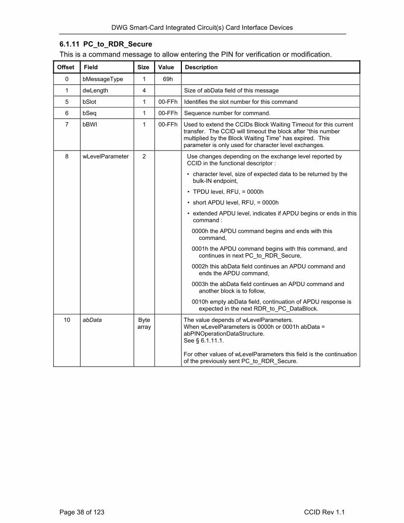
DWG Smart-Card Integrated Circuit(s) Card Interface Devices 6.1.11 PC_to_RDR_Secure This is a command message to allow entering the PIN for verification or modification.
Offset Field Size Value Description
0 bMessageType 1 69h
1 dwLength 4 Size of abData field of this message
5 bSlot 1 00-FFh Identifies the slot number for this command
6 bSeq 1 00-FFh Sequence number for command.
7 bBWI 1 00-FFh Used to extend the CCIDs Block Waiting Timeout for this current transfer. The CCID will timeout the block after “this number multiplied by the Block Waiting Time” has expired. This parameter is only used for character level exchanges.
8 wLevelParameter 2 Use changes depending on the exchange level reported by CCID in the functional descriptor :
• character level, size of expected data to be returned by the bulk-IN endpoint,
• TPDU level, RFU, = 0000h
• short APDU level, RFU, = 0000h
• extended APDU level, indicates if APDU begins or ends in this command :
0000h the APDU command begins and ends with this command,
0001h the APDU command begins with this command, and continues in next PC_to_RDR_Secure,
0002h this abData field continues an APDU command and ends the APDU command,
0003h the abData field continues an APDU command and another block is to follow,
0010h empty abData field, continuation of APDU response is expected in the next RDR_to_PC_DataBlock.
10 abData Byte array
The value depends of wLevelParameters. When wLevelParameters is 0000h or 0001h abData = abPINOperationDataStructure. See § 6.1.11.1. For other values of wLevelParameters this field is the continuation of the previously sent PC_to_RDR_Secure.
Page 38 of 123 CCID Rev 1.1
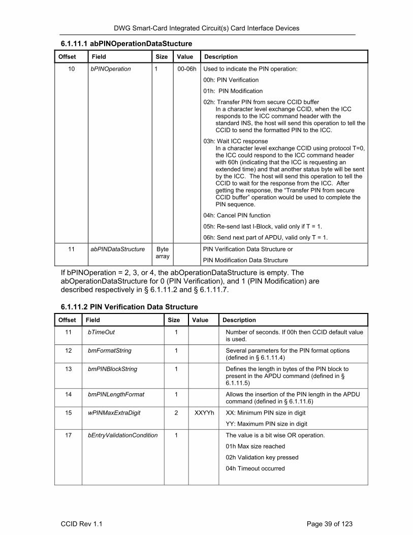
DWG Smart-Card Integrated Circuit(s) Card Interface Devices 6.1.11.1 abPINOperationDataStucture
Offset Field Size Value Description
10 bPINOperation 1 00-06h Used to indicate the PIN operation:
00h: PIN Verification
01h: PIN Modification
02h: Transfer PIN from secure CCID buffer In a character level exchange CCID, when the ICC responds to the ICC command header with the standard INS, the host will send this operation to tell the CCID to send the formatted PIN to the ICC.
03h: Wait ICC response In a character level exchange CCID using protocol T=0, the ICC could respond to the ICC command header with 60h (indicating that the ICC is requesting an extended time) and that another status byte will be sent by the ICC. The host will send this operation to tell the CCID to wait for the response from the ICC. After getting the response, the “Transfer PIN from secure CCID buffer” operation would be used to complete the PIN sequence.
04h: Cancel PIN function
05h: Re-send last I-Block, valid only if T = 1.
06h: Send next part of APDU, valid only T = 1.
11 abPINDataStructure Byte array
PIN Verification Data Structure or
PIN Modification Data Structure
If bPINOperation = 2, 3, or 4, the abOperationDataStructure is empty. The abOperationDataStructure for 0 (PIN Verification), and 1 (PIN Modification) are described respectively in § 6.1.11.2 and § 6.1.11.7. 6.1.11.2 PIN Verification Data Structure
Offset Field Size Value Description
11 bTimeOut 1 Number of seconds. If 00h then CCID default value is used.
12 bmFormatString 1 Several parameters for the PIN format options (defined in § 6.1.11.4)
13 bmPINBlockString 1 Defines the length in bytes of the PIN block to present in the APDU command (defined in § 6.1.11.5)
14 bmPINLengthFormat 1 Allows the insertion of the PIN length in the APDU command (defined in § 6.1.11.6)
15 wPINMaxExtraDigit 2 XXYYh XX: Minimum PIN size in digit
YY: Maximum PIN size in digit
17 bEntryValidationCondition 1 The value is a bit wise OR operation.
01h Max size reached
02h Validation key pressed
04h Timeout occurred
CCID Rev 1.1 Page 39 of 123
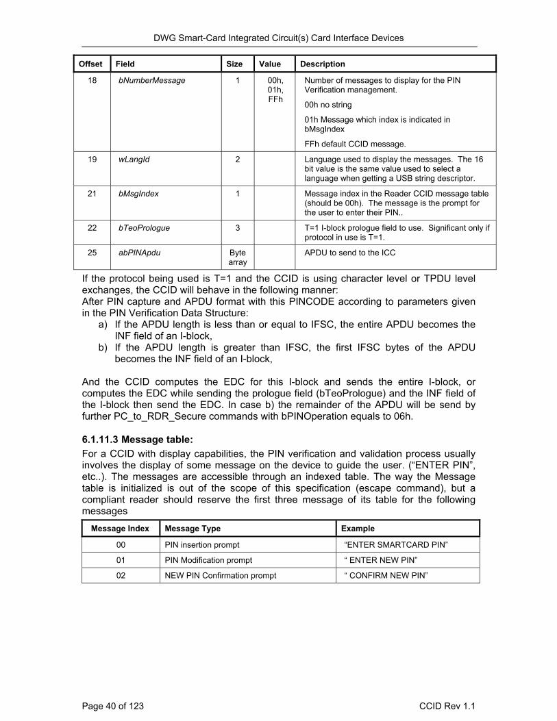
DWG Smart-Card Integrated Circuit(s) Card Interface Devices
Offset Field Size Value Description
18 bNumberMessage 1 00h, 01h, FFh
Number of messages to display for the PIN Verification management.
00h no string
01h Message which index is indicated in bMsgIndex
FFh default CCID message.
19 wLangId 2 Language used to display the messages. The 16 bit value is the same value used to select a language when getting a USB string descriptor.
21 bMsgIndex 1 Message index in the Reader CCID message table (should be 00h). The message is the prompt for the user to enter their PIN..
22 bTeoPrologue 3 T=1 I-block prologue field to use. Significant only if protocol in use is T=1.
25 abPINApdu Byte array
APDU to send to the ICC
If the protocol being used is T=1 and the CCID is using character level or TPDU level exchanges, the CCID will behave in the following manner: After PIN capture and APDU format with this PINCODE according to parameters given in the PIN Verification Data Structure:
a) If the APDU length is less than or equal to IFSC, the entire APDU becomes the INF field of an I-block,
b) If the APDU length is greater than IFSC, the first IFSC bytes of the APDU becomes the INF field of an I-block,
And the CCID computes the EDC for this I-block and sends the entire I-block, or computes the EDC while sending the prologue field (bTeoPrologue) and the INF field of the I-block then send the EDC. In case b) the remainder of the APDU will be send by further PC_to_RDR_Secure commands with bPINOperation equals to 06h. 6.1.11.3 Message table: For a CCID with display capabilities, the PIN verification and validation process usually involves the display of some message on the device to guide the user. (“ENTER PIN”, etc..). The messages are accessible through an indexed table. The way the Message table is initialized is out of the scope of this specification (escape command), but a compliant reader should reserve the first three message of its table for the following messages
Message Index Message Type Example
00 PIN insertion prompt “ENTER SMARTCARD PIN”
01 PIN Modification prompt “ ENTER NEW PIN”
02 NEW PIN Confirmation prompt “ CONFIRM NEW PIN”
Page 40 of 123 CCID Rev 1.1
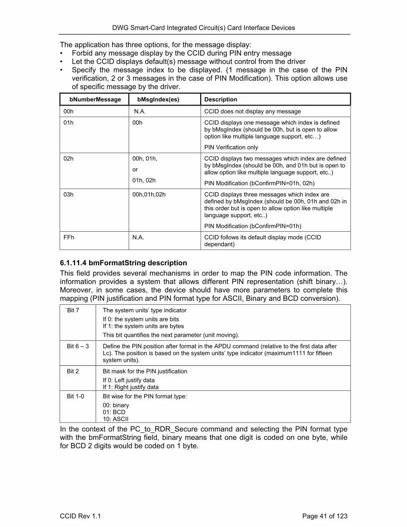
DWG Smart-Card Integrated Circuit(s) Card Interface Devices
The application has three options, for the message display: • Forbid any message display by the CCID during PIN entry message • Let the CCID displays default(s) message without control from the driver • Specify the message index to be displayed. (1 message in the case of the PIN
verification, 2 or 3 messages in the case of PIN Modification). This option allows use of specific message by the driver.
bNumberMessage bMsgIndex(es) Description
00h N.A. CCID does not display any message
01h 00h CCID displays one message which index is defined by bMsgIndex (should be 00h, but is open to allow option like multiple language support, etc…)
PIN Verification only
02h 00h, 01h,
or
01h, 02h
CCID displays two messages which index are defined by bMsgIndex (should be 00h, and 01h but is open to allow option like multiple language support, etc..)
PIN Modification (bConfirmPIN=01h, 02h)
03h 00h,01h,02h CCID displays three messages which index are defined by bMsgIndex (should be 00h, 01h and 02h in this order but is open to allow option like multiple language support, etc..)
PIN Modification (bConfirmPIN=01h)
FFh N.A. CCID follows its default display mode (CCID dependant)
6.1.11.4 bmFormatString description This field provides several mechanisms in order to map the PIN code information. The information provides a system that allows different PIN representation (shift binary…). Moreover, in some cases, the device should have more parameters to complete this mapping (PIN justification and PIN format type for ASCII, Binary and BCD conversion).
`Bit 7 The system units’ type indicator If 0: the system units are bits If 1: the system units are bytes This bit quantifies the next parameter (unit moving).
Bit 6 – 3 Define the PIN position after format in the APDU command (relative to the first data after Lc). The position is based on the system units’ type indicator (maximum1111 for fifteen system units).
Bit 2 Bit mask for the PIN justification If 0: Left justify data If 1: Right justify data
Bit 1-0 Bit wise for the PIN format type: 00: binary 01: BCD 10: ASCII
In the context of the PC_to_RDR_Secure command and selecting the PIN format type with the bmFormatString field, binary means that one digit is coded on one byte, while for BCD 2 digits would be coded on 1 byte.
CCID Rev 1.1 Page 41 of 123
DWG Smart-Card Integrated Circuit(s) Card Interface Devices Example: If the PIN presented is 12345: bmFormatString bits 1-0 = Binary --> the command to the ICC is going to look like <Command header> <length> 01 02 03 04 05 .... bmFormatString bits 1-0 = BCD --> the command to the ICC is going to look like <Command header> <length> 12 34 5X .... (where X represents the padding character) 6.1.11.5 bmPINBlockString This field provides the PIN block size and the PIN length size information.
Bit 7 - 4 Size in bits of the PIN length inserted in the APDU command. (If 0h, then the effective pin length is not inserted in the APDU command)
Bit 3 - 0 PIN length information: PIN block size in bytes after justification and formatting.
6.1.11.6 bmPINLengthFormat Some ICCs include the effective PIN length in their APDU command (EMV ICCs for example). The bmPINLengthFormat provides the PIN length position in the APDU command.
Bit 7-5 RFU
Bit 4 The system units’ type indicator If 0: the system units are bits If 1: the system units are bytes
Bit 3 - 0 Indicate the PIN length position in the APDU command according to the previous parameters (maximum 1111 for fifteen system units).
Page 42 of 123 CCID Rev 1.1
DWG Smart-Card Integrated Circuit(s) Card Interface Devices 6.1.11.7 PIN Modification Data Structure
Offset Field Size Value Description
11 bTimeOut 1 Number of seconds. If 00h then CCID default value is used.
12 bmFormatString4 1 Several parameters for the PIN format options (defined in § 6.1.11.4)
13 bmPINBlockString 1 Define the length of the PIN to present in the APDU command
14 bmPinLengthFormat 1 Allows the length PIN insertion in the APDU command (defined in § 6.1.11.6)
15 bInsertionOffsetOld 1 Insertion position offset in byte for the current PIN 16 bInsertionOffsetNew 1 Insertion position offset in byte for the new PIN 17 wPINMaxExtraDigit 2 XXYYh XX: Minimum PIN size in digit
YY: Maximum PIN size in digit
19 bConfirmPIN 1 00h, 01h 02h, 03h.
Indicates if a confirmation is requested before acceptance of a new PIN (meaning that the user has to enter this new PIN twice before it is accepted)
Indicates if the current PIN must be entered and set in the same APDU field of not.
b0: (0/1)
If 0 = No confirmation requested
If 1 = Confirmation requested
b1: (0/1)
If 0 = No current PIN entry requested. (In this case, the bInsertinoOffsetOld value mustn’t be taken into account.)
If 1 = Current PIN entry requested
b2 – b7 : RFU
20 bEntryValidationCondition 1 The value is a bit wise OR operation. 01h Max size reached 02h Validation key pressed 04h Timeout occurred
21 bNumberMessage 1 00h, 01h, 02h, 03h,
or FFh
Number of messages to display for the PIN modify command. 00h: no message.
01h: Message which index is indicated in bMsgIndex1 (case where bConfirmPIN = 00h)
02h Messages which index are indicated in bMsgIndex1, and bMsgIndex2 (case where bConfirmPIN = 01h or 02h)
03h Messages which index are indicated in bMsgIndex1, bMsgIndex2, and bMsgIndex3 (case where bConfirmPIN = 03h) FFh default CCID message(s)
22 wLangId 2 Language used to display the messages. The 16 bit
4 Some ICC uses a shift bit mechanism to format the PIN. In this case the PIN position parameters in the bFormatString are not redundant with the bInsertionOffsetOld or bInsertionOffsetNew.
CCID Rev 1.1 Page 43 of 123
DWG Smart-Card Integrated Circuit(s) Card Interface Devices
Offset Field Size Value Description value is the same value used to select a language when getting a USB string descriptor.
24 bMsgIndex1 1 Message index in the Reader message table (should be 00h or 01h).
The message is the prompt for the user to enter its new PIN if bConfirmPIN=00h or its current PIN..
25 bMsgIndex2 1 Message index in the Reader message table (should be 01h or 02h). The message is the prompt for the user to enter its new PIN value if bConfirm-02h or 03h, and to re-enter its new PIN if bConfirm=01h. (only present if bNumberMessage is not null)
26 bMsgIndex3 1 Message index in the Reader message table (should be 02h).
The message is the prompt for the user to re-enter its new PIN value for confirmation purposes (only present if bNumberMessage = 3)
25 or 26 or
27
bTeoPrologue 3 T=1 I-block prologue field to use. Significant only if protocol in use is T=1.
28 or 29 or
30
abPINApdu Byte array
APDU to send to the ICC
If the protocol being used is T=1 and the CCID is using character level or TPDU level exchanges, the CCID will behave in the following manner: After new pin capture (and confirmation if requested) and APDU format with the PIN(s) value(s) according to parameters given in the PIN Modification Data Structure :
a) If the APDU length is less than or equal to IFSC, the entire APDU becomes the INF field of an I-block,
b) If the APDU length is greater than IFSC, The first IFSC bytes of the APDU becomes the INF field of an I-block,
and the CCID computes the EDC for this I-block and sends the entire I-block, or computes the EDC while sending the prologue field (bTeoPrologue)and the INF field of the I-block then send the EDC. In case b) the remainder of the APDU will be send by further PC_to_RDR_Secure commands with bPINOperation equals to 06h. In order to provide an efficient security to avoid PIN violation, only the INS ICC command for PIN verification or PIN modification is valid for the PC_to_RDR_Secure message. The CCID should reject any INS ICC command which is not 20h (Verify), or 24h (PIN change/unblock).
The wLangId field supports displaying messages in multiple languages. The requester specifies the desired language by using a sixteen-bit language id (LANGID defined by the USB-IF. The list of currently defined USB LANGIDs can be found at http://www.usb.org/developers/docs.html.. To determine what languages the CCID
Page 44 of 123 CCID Rev 1.1
DWG Smart-Card Integrated Circuit(s) Card Interface Devices supports, a standard request of Get Descriptor for String Index 0 for all languages returns an array of the two-byte LANGID codes supported by the CCID. 6.1.11.8 Send Next Part of APDU Data Structure
Offset Field Size Value Description
11 bTeoPrologue 3 T=1 I-block prologue field to use. Significant only if protocol in use is T=1.
6.1.11.9 Remarks on character level or TPDU level when T = 1 For a CCID working at character level or at TPDU level when T=1, both of the following behaviors are valid. It is up to the CCID designer to select one.
1. Accept PC_to_Reader_Secure requests with bPINOperation equal to 05h or 06h and do the required behavior. OR
2. Fail a PC_to_RDR_Secure when the APDU size exceeds the IFSC, indicating the offset of bTeoPrologue field and fail a PC_to_RDR_Secure with bPINOperation equal to 06h, indicating the offset of bPINOperation field.
6.1.11.10 Response to PC_to_RDR_Secure The response to this command message is the RDR_to_PC_DataBlock response message. RDR_to_PC_DataBlock could return any of the following errors.
bmICCStatus bmCommandStatus bError Description
2 1 5 bSlot does not exist
2 1 ICC_MUTE No ICC present
1 1 BUSY_WITH_AUTO_SEQUENCE Automatic sequence on-going
1 1 HW_ERROR Hardware error
0 1 0 Command Not Supported
0,1,2 1 CMD_SLOT_BUSY
1 1 XFR_PARITY_ERROR parity error on ATR
1 1 ICC_MUTE ICC mute (Time out)
1 1 CMD_ABORTED Command aborted by control pipe
0 1 0 Command Not Supported
CCID Rev 1.1 Page 45 of 123

DWG Smart-Card Integrated Circuit(s) Card Interface Devices 6.1.12 PC_to_RDR_Mechanical This command is used to manage motorized type CCID functionality. The Lock Card function is used to hold the ICC. This prevents an ICC from being easily removed from the CCID. The Unlock Card function is used to remove the hold initiated by the Lock Card function
Offset Field Size Value Description
0 bMessageType 1 71h
1 dwLength 4 00000000h Message-specific data length
5 bSlot 1 00-FFh Identifies the slot number for this command
6 bSeq 1 00-FFh Sequence number for command.
7 bFunction 1 04h-05h This value corresponds to the mechanical function being requested
01h – Accept Card
02h – Eject Card
03h – Capture Card
04h – Lock Card
05h – Unlock Card
Values 01-03h are included for completeness but these functions are not covered by this release of the specification
8 abRFU 2 00h Reserved for Future Use
The response to this command message is the RDR_to_PC_SlotStatus response message. RDR_to_PC_SlotStatus could return any of the following errors.
bmICCStatus bmCommandStatus bError Description
2 1 5 bSlot does not exist
2 1 ICC_MUTE No ICC present
1 1 BUSY_WITH_AUTO_SEQUENCE Automatic sequence on-going
1 1 HW_ERROR Hardware error
0 1 0 Command Not Supported
0,1,2 1 CMD_SLOT_BUSY
Page 46 of 123 CCID Rev 1.1
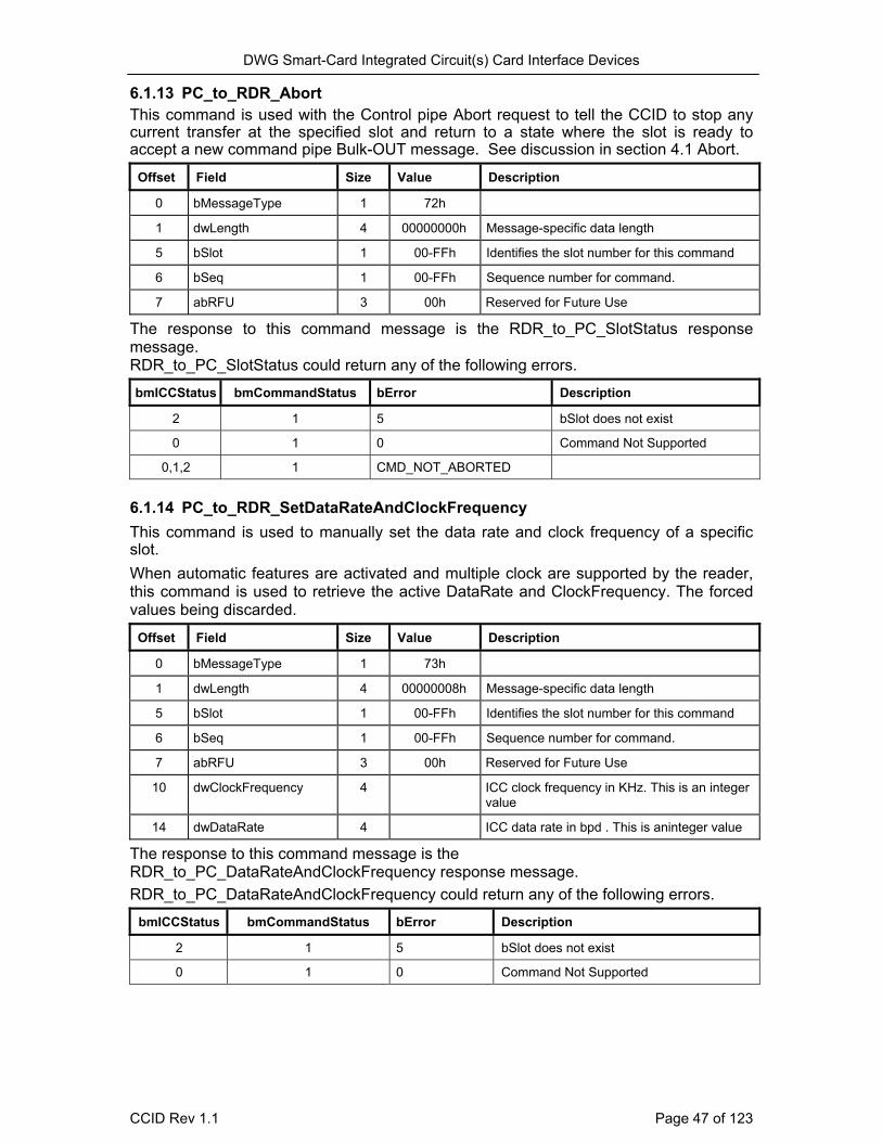
DWG Smart-Card Integrated Circuit(s) Card Interface Devices 6.1.13 PC_to_RDR_Abort This command is used with the Control pipe Abort request to tell the CCID to stop any current transfer at the specified slot and return to a state where the slot is ready to accept a new command pipe Bulk-OUT message. See discussion in section 4.1 Abort.
Offset Field Size Value Description
0 bMessageType 1 72h
1 dwLength 4 00000000h Message-specific data length
5 bSlot 1 00-FFh Identifies the slot number for this command
6 bSeq 1 00-FFh Sequence number for command.
7 abRFU 3 00h Reserved for Future Use
The response to this command message is the RDR_to_PC_SlotStatus response message. RDR_to_PC_SlotStatus could return any of the following errors.
bmICCStatus bmCommandStatus bError Description
2 1 5 bSlot does not exist
0 1 0 Command Not Supported
0,1,2 1 CMD_NOT_ABORTED
6.1.14 PC_to_RDR_SetDataRateAndClockFrequency This command is used to manually set the data rate and clock frequency of a specific slot. When automatic features are activated and multiple clock are supported by the reader, this command is used to retrieve the active DataRate and ClockFrequency. The forced values being discarded.
Offset Field Size Value Description
0 bMessageType 1 73h
1 dwLength 4 00000008h Message-specific data length
5 bSlot 1 00-FFh Identifies the slot number for this command
6 bSeq 1 00-FFh Sequence number for command.
7 abRFU 3 00h Reserved for Future Use
10 dwClockFrequency 4 ICC clock frequency in KHz. This is an integer value
14 dwDataRate 4 ICC data rate in bpd . This is aninteger value
The response to this command message is the RDR_to_PC_DataRateAndClockFrequency response message. RDR_to_PC_DataRateAndClockFrequency could return any of the following errors.
bmICCStatus bmCommandStatus bError Description
2 1 5 bSlot does not exist
0 1 0 Command Not Supported
CCID Rev 1.1 Page 47 of 123
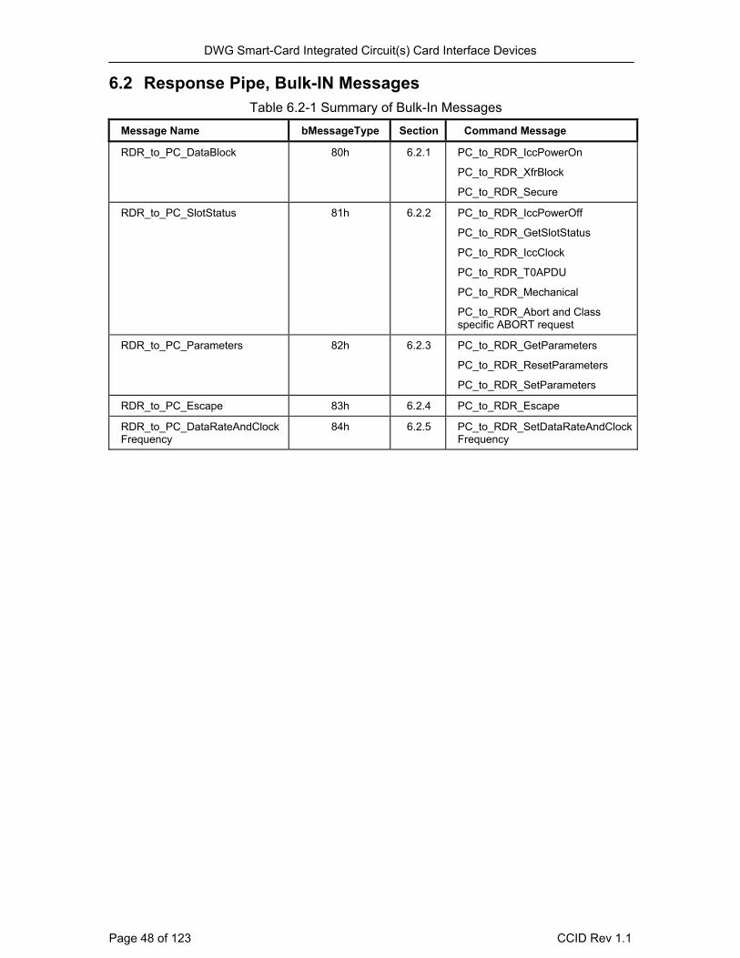
DWG Smart-Card Integrated Circuit(s) Card Interface Devices 6.2 Response Pipe, Bulk-IN Messages
Table 6.2-1 Summary of Bulk-In Messages
Message Name bMessageType Section Command Message
RDR_to_PC_DataBlock 80h 6.2.1 PC_to_RDR_IccPowerOn
PC_to_RDR_XfrBlock
PC_to_RDR_Secure
RDR_to_PC_SlotStatus 81h
6.2.2 PC_to_RDR_IccPowerOff
PC_to_RDR_GetSlotStatus
PC_to_RDR_IccClock
PC_to_RDR_T0APDU
PC_to_RDR_Mechanical
PC_to_RDR_Abort and Class specific ABORT request
RDR_to_PC_Parameters 82h 6.2.3 PC_to_RDR_GetParameters
PC_to_RDR_ResetParameters
PC_to_RDR_SetParameters
RDR_to_PC_Escape 83h 6.2.4 PC_to_RDR_Escape
RDR_to_PC_DataRateAndClockFrequency
84h 6.2.5 PC_to_RDR_SetDataRateAndClockFrequency
Page 48 of 123 CCID Rev 1.1

DWG Smart-Card Integrated Circuit(s) Card Interface Devices 6.2.1 RDR_to_PC_DataBlock The device in response to the following command messages: “PC_to_RDR_IccPowerOn”, “PC_to_RDR_Secure” and “PC_to_RDR_XfrBlock” sends this response message. For “PC_to_RDR_IccPowerOn” this response message is the answer to reset (ATR) data associated with the ICC power on. In other cases, the response message has the following format: The response data will contain the optional data returned by the ICC, followed by the 2 byte-size status words SW1-SW2.
Offset Field Size Value Description
0 bMessageType 1 80h Indicates that a data block is being sent from the CCID
1 dwLength 4 Size of abData field of this message
5 bSlot 1 Same as Bulk-OUT message
Identifies the slot number for this command
6 bSeq 1 Same as Bulk-OUT message
Sequence number for the corresponding command.
7 bStatus 1 Slot status register as defined in § 6.2.6
8 bError 1 Slot error register as defined in § 6.2.6
9 bChainParameter 1 Depends on the exchange level reported by the class descriptor in dwFeatures field:
Character level, TPDU level, short APDU level, this field is RFU and =00h.
Extended APDU level, indicates if the response is complete, to be continued or if the command APDU can continue 00h the response APDU begins and ends in this command 01h the response APDU begins with this command and is to continue 02h this abData field continues the response APDU and ends the response APDU 03h this abData field continues the response APDU and another block is to follow 10h empty abData field, continuation of the command APDU is expected in next PC_to_RDR_XfrBlock command
10 abData Byte array
This field contains the data returned by the CCID. Depending on the exchange level, this may be data and status “as is” from the ICC, or the CCID may “filter” the data and status before sending it to the host. It can be 0 - 65,538 bytes in length
CCID Rev 1.1 Page 49 of 123
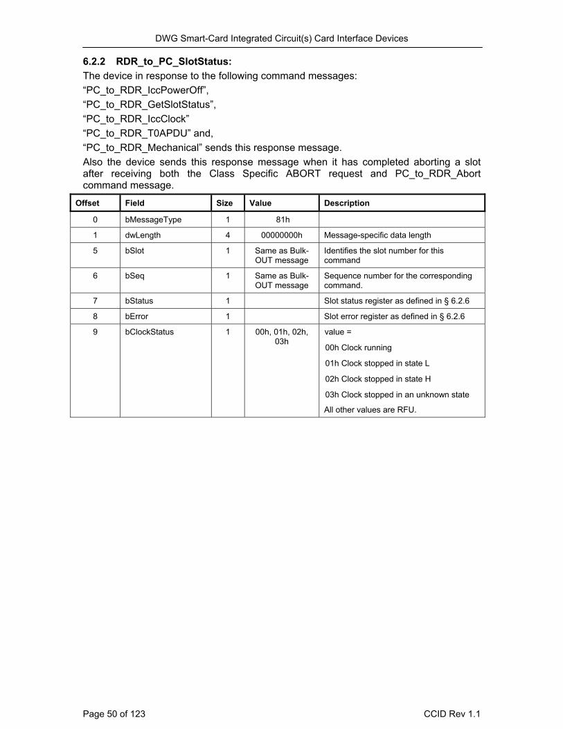
DWG Smart-Card Integrated Circuit(s) Card Interface Devices 6.2.2 RDR_to_PC_SlotStatus: The device in response to the following command messages: “PC_to_RDR_IccPowerOff”, “PC_to_RDR_GetSlotStatus”, “PC_to_RDR_IccClock” “PC_to_RDR_T0APDU” and, “PC_to_RDR_Mechanical” sends this response message. Also the device sends this response message when it has completed aborting a slot after receiving both the Class Specific ABORT request and PC_to_RDR_Abort command message.
Offset Field Size Value Description
0 bMessageType 1 81h
1 dwLength 4 00000000h Message-specific data length
5 bSlot 1 Same as Bulk-OUT message
Identifies the slot number for this command
6 bSeq 1 Same as Bulk-OUT message
Sequence number for the corresponding command.
7 bStatus 1 Slot status register as defined in § 6.2.6
8 bError 1 Slot error register as defined in § 6.2.6
9 bClockStatus 1 00h, 01h, 02h, 03h
value =
00h Clock running
01h Clock stopped in state L
02h Clock stopped in state H
03h Clock stopped in an unknown state
All other values are RFU.
Page 50 of 123 CCID Rev 1.1
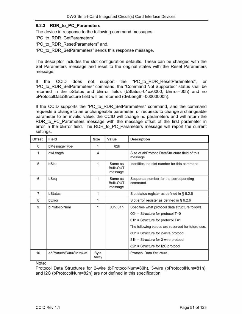
DWG Smart-Card Integrated Circuit(s) Card Interface Devices 6.2.3 RDR_to_PC_Parameters The device in response to the following command messages: “PC_to_RDR_GetParameters”, “PC_to_RDR_ResetParameters” and, “PC_to_RDR_SetParameters” sends this response message. The descriptor includes the slot configuration defaults. These can be changed with the Set Parameters message and reset to the original states with the Reset Parameters message. If the CCID does not support the “PC_to_RDR_ResetParameters”, or “PC_to_RDR_SetParameters” command, the “Command Not Supported” status shall be returned in the bStatus and bError fields (bStatus=01xx0000, bError=00h) and no bProtocolDataStructure field will be returned (dwLength=00000000h). If the CCID supports the “PC_to_RDR_SetParameters” command, and the command requests a change to an unchangeable parameter, or requests to change a changeable parameter to an invalid value, the CCID will change no parameters and will return the RDR_to_PC_Parameters message with the message offset of the first parameter in error in the bError field. The RDR_to_PC_Parameters message will report the current settings.
Offset Field Size Value Description
0 bMessageType 1 82h
1 dwLength 4 Size of abProtocolDataStructure field of this message
5 bSlot 1 Same as Bulk-OUT message
Identifies the slot number for this command
6 bSeq 1 Same as Bulk-OUT message
Sequence number for the corresponding command.
7 bStatus 1 Slot status register as defined in § 6.2.6
8 bError 1 Slot error register as defined in § 6.2.6
9 bProtocolNum 1 00h, 01h Specifies what protocol data structure follows.
00h = Structure for protocol T=0
01h = Structure for protocol T=1
The following values are reserved for future use.
80h = Structure for 2-wire protocol
81h = Structure for 3-wire protocol
82h = Structure for I2C protocol
10 abProtocolDataStructure Byte Array
Protocol Data Structure
Note: Protocol Data Structures for 2-wire (bProtocolNum=80h), 3-wire (bProtocolNum=81h), and I2C (bProtocolNum=82h) are not defined in this specification.
CCID Rev 1.1 Page 51 of 123

DWG Smart-Card Integrated Circuit(s) Card Interface Devices Protocol Data Structure for Protocol T=0 (bProtocolNum=0, dwLength=00000005h)
Offset Field Size Value Description
10 bmFindexDindex
1
B7-4 – FI – Index into the table 7 in ISO/IEC 7816-3:1997 selecting a clock rate conversion factor
B3-0 – DI - Index into the table 8 in ISO/IEC 7816-3:1997 selecting a baud rate conversion factor
11 bmTCCKST0 1
00h, 02h For T=0 ,B0 – 0b, B7-2 – 000000b
B1 – Convention used (b1=0 for direct, b1=1 for inverse)
12 bGuardTimeT0 1
00-FFh Extra Guardtime between two characters. Add 0 to 254 etu to the normal guardtime of 12etu. FFh is the same as 00h.
13 bWaitingIntegerT0 1 00-FFh WI for T=0 used to define WWT
14 bClockStop
1
00-03h ICC Clock Stop Support
00 = Stopping the Clock is not allowed
01 = Stop with Clock signal Low
02 = Stop with Clock signal High
03 = Stop with Clock either High or Low
Protocol Data Structure for Protocol T=1 (bProtocolNum=1, dwLength=00000007h)
Offset Field Size Value Description
10 bmFindexDindex 1 B7-4 – FI – Index into the table 7 in ISO/IEC 7816-3:1997 selecting a clock rate conversion factor
B3-0 – DI - Index into the table 8 in ISO/IEC 7816-3:1997 selecting a baud rate conversion factor
11 bmTCCKST1 1 10h, 11h, 12h, 13h
For T=1, B7-2 – 000100b
B0 – Checksum type (b0=0 for LRC, b0=1 for CRC
B1 – Convention used (b1=0 for direct, b1=1 for inverse)
12 bGuardTimeT1 1 00-FFh Extra Guardtime (0 to 254 etu between two characters). If value is FFh, then guardtime is reduced by 1.
13 bmWaitingIntegersT1 1 00-9Fh B7-4 = BWI
B3-0 = CWI
14 bClockStop 1 00-03h ICC Clock Stop Support
00 = Stopping the Clock is not allowed
01 = Stop with Clock signal Low
02 = Stop with Clock signal High
03 = Stop with Clock either High or Low
15 bIFSC 1 00-FEh Size of negotiated IFSC
16 bNadValue 1 00-FFh Nad value used by CCID
Page 52 of 123 CCID Rev 1.1
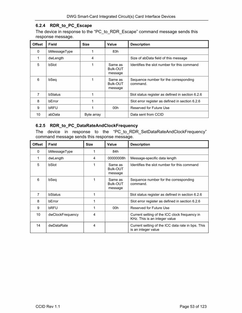
DWG Smart-Card Integrated Circuit(s) Card Interface Devices 6.2.4 RDR_to_PC_Escape The device in response to the “PC_to_RDR_Escape” command message sends this response message.
Offset Field Size Value Description
0 bMessageType 1 83h
1 dwLength 4 Size of abData field of this message
5 bSlot 1 Same as Bulk-OUT message
Identifies the slot number for this command
6 bSeq 1 Same as Bulk-OUT message
Sequence number for the corresponding command.
7 bStatus 1 Slot status register as defined in section 6.2.6
8 bError 1 Slot error register as defined in section 6.2.6
9 bRFU 1 00h Reserved for Future Use
10 abData Byte array Data sent from CCID
6.2.5 RDR_to_PC_DataRateAndClockFrequency The device in response to the “PC_to_RDR_SetDataRateAndClockFrequency” command message sends this response message.
Offset Field Size Value Description
0 bMessageType 1 84h
1 dwLength 4 00000008h Message-specific data length
5 bSlot 1 Same as Bulk-OUT message
Identifies the slot number for this command
6 bSeq 1 Same as Bulk-OUT message
Sequence number for the corresponding command.
7 bStatus 1 Slot status register as defined in section 6.2.6
8 bError 1 Slot error register as defined in section 6.2.6
9 bRFU 1 00h Reserved for Future Use
10 dwClockFrequency 4 Current setting of the ICC clock frequency in KHz. This is an integer value
14 dwDataRate 4 Current setting of the ICC data rate in bps. This is an integer value
CCID Rev 1.1 Page 53 of 123
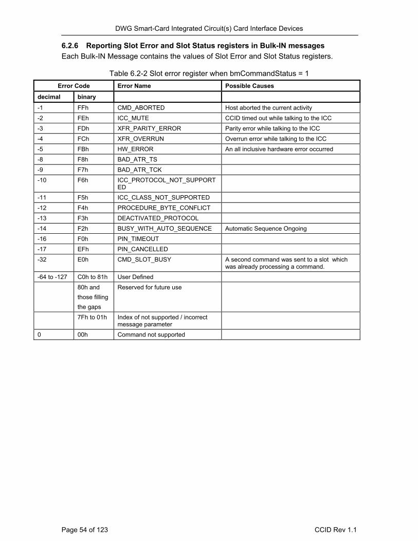
DWG Smart-Card Integrated Circuit(s) Card Interface Devices 6.2.6 Reporting Slot Error and Slot Status registers in Bulk-IN messages Each Bulk-IN Message contains the values of Slot Error and Slot Status registers.
Table 6.2-2 Slot error register when bmCommandStatus = 1 Error Code Error Name Possible Causes
decimal binary
-1 FFh CMD_ABORTED Host aborted the current activity
-2 FEh ICC_MUTE CCID timed out while talking to the ICC
-3 FDh XFR_PARITY_ERROR Parity error while talking to the ICC
-4 FCh XFR_OVERRUN Overrun error while talking to the ICC
-5 FBh HW_ERROR An all inclusive hardware error occurred
-8 F8h BAD_ATR_TS
-9 F7h BAD_ATR_TCK
-10 F6h ICC_PROTOCOL_NOT_SUPPORTED
-11 F5h ICC_CLASS_NOT_SUPPORTED
-12 F4h PROCEDURE_BYTE_CONFLICT
-13 F3h DEACTIVATED_PROTOCOL
-14 F2h BUSY_WITH_AUTO_SEQUENCE Automatic Sequence Ongoing
-16 F0h PIN_TIMEOUT
-17 EFh PIN_CANCELLED
-32 E0h CMD_SLOT_BUSY A second command was sent to a slot which was already processing a command.
-64 to -127 C0h to 81h User Defined
80h and those filling the gaps
Reserved for future use
7Fh to 01h Index of not supported / incorrect message parameter
0 00h Command not supported
Page 54 of 123 CCID Rev 1.1
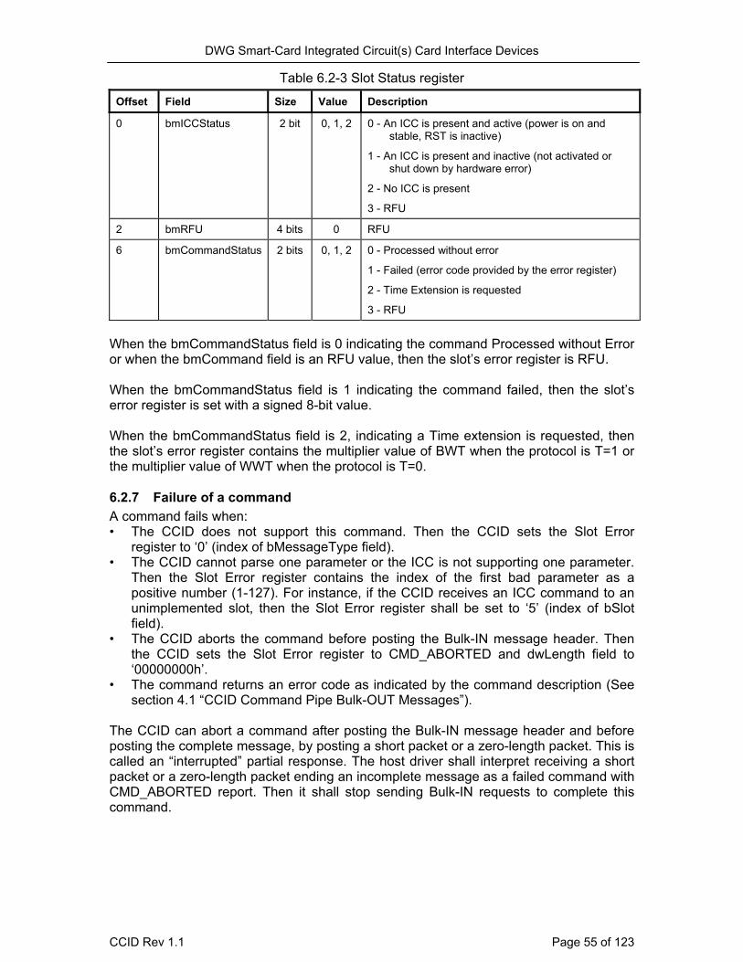
DWG Smart-Card Integrated Circuit(s) Card Interface Devices
Table 6.2-3 Slot Status register
Offset Field Size Value Description
0 bmICCStatus 2 bit 0, 1, 2 0 - An ICC is present and active (power is on and stable, RST is inactive)
1 - An ICC is present and inactive (not activated or shut down by hardware error)
2 - No ICC is present
3 - RFU
2 bmRFU 4 bits 0 RFU
6 bmCommandStatus 2 bits 0, 1, 2 0 - Processed without error
1 - Failed (error code provided by the error register)
2 - Time Extension is requested
3 - RFU
When the bmCommandStatus field is 0 indicating the command Processed without Error or when the bmCommand field is an RFU value, then the slot’s error register is RFU. When the bmCommandStatus field is 1 indicating the command failed, then the slot’s error register is set with a signed 8-bit value. When the bmCommandStatus field is 2, indicating a Time extension is requested, then the slot’s error register contains the multiplier value of BWT when the protocol is T=1 or the multiplier value of WWT when the protocol is T=0. 6.2.7 Failure of a command A command fails when: • The CCID does not support this command. Then the CCID sets the Slot Error
register to ‘0’ (index of bMessageType field). • The CCID cannot parse one parameter or the ICC is not supporting one parameter.
Then the Slot Error register contains the index of the first bad parameter as a positive number (1-127). For instance, if the CCID receives an ICC command to an unimplemented slot, then the Slot Error register shall be set to ‘5’ (index of bSlot field).
• The CCID aborts the command before posting the Bulk-IN message header. Then the CCID sets the Slot Error register to CMD_ABORTED and dwLength field to ‘00000000h’.
• The command returns an error code as indicated by the command description (See section 4.1 “CCID Command Pipe Bulk-OUT Messages”).
The CCID can abort a command after posting the Bulk-IN message header and before posting the complete message, by posting a short packet or a zero-length packet. This is called an “interrupted” partial response. The host driver shall interpret receiving a short packet or a zero-length packet ending an incomplete message as a failed command with CMD_ABORTED report. Then it shall stop sending Bulk-IN requests to complete this command.
CCID Rev 1.1 Page 55 of 123
DWG Smart-Card Integrated Circuit(s) Card Interface Devices 6.3 Interrupt-IN Messages The Interrupt-IN endpoint is used to notify the host of events that may occur asynchronously and outside the context of a command-response exchange between host and CCID. If the host has sent a Bulk-Out message and is waiting for a Bulk-IN message in response, and one of these events occurs, then the Bulk-IN message may have duplicate information related to the event.
Table 6.3-1 . Summary of Interrupt-In Messages Message Name bMessageType Section
RDR_to_PC_NotifySlotChange 50h 6.3.1
RDR_to_PC_HardwareError 51h 6.3.2
6.3.1 RDR_to_PC_NotifySlotChange This message is sent whenever the CCID device detects a change in the insertion status of an ICC slot. If an ICC is either inserted or removed from a slot, this message must be sent. The presence of this message means to the host driver that a change has occurred. It is possible for more than one change to occur between deliveries of RDR_to_PC_NotifySlotChange messages. When 1) a configuration other then ‘0’ is selected or 2) when the USB bus is resumed from a suspended state, both the CCID and the host driver must make identical assumptions about the state of the ICC slots. For simplicity, this specification requires that both CCID and host driver shall presume that all slots are empty. Therefore, after either a configuration change or resumption from suspend, the CCID shall report all occupied ICC slots using this message cf. § 3.3. Offset Field Size Value Description
0 bMessageType 1 50h
1 bmSlotICCState This field is reported on byte granularity.
The size is ( 2 bits * number of slots ) rounded up to the nearest byte.
Each slot has 2 bits. The least significant bit reports the current state of the slot (0b = no ICC present, 1b = ICC present). The most significant bit reports whether the slot has changed state since the last RDR_to_PC_NotifySlotChange message was sent (0b = no change, 1b = change).
If no slot exists for a given location, the field returns 00b in those 2 bits.
Example: A 3 slot CCID reports a single byte with the following format: Bit 0 = Slot 0 current state Bit 1 = Slot 0 changed status Bit 2 = Slot 1 current state Bit 3 = Slot 1 changed status Bit 4 = Slot 2 current state Bit 5 = Slot 2 changed status Bit 6 = 0b Bit 7 = 0b
Page 56 of 123 CCID Rev 1.1

DWG Smart-Card Integrated Circuit(s) Card Interface Devices 6.3.2 RDR_to_PC_HardwareError This message is sent when any bit in the bHardwareErrorCode field is set. If this message is sent when there is no “outstanding” command, the bSeq field will be undefined. When a CCID detects an over current condition, it will do the following. The CCID will deactivate the slot with the over current. If the CCID supports this message, it will send this message. If a Bulk-OUT command is active on the slot that has the over current, then that command is stopped and the inactive state of the slot and an over current error is returned in the bStatus and bError fields of the Bulk-IN response for that command. If the CCID does not support this message and an error condition occurs, then the condition will be reported on the next Bulk-Out command.
Offset Field Size Value Description
0 bMessageType 1 51h
1 bSlot 1 00h-FFh ICC slot number
2 bSeq 1 00h-FFh Sequence number of bulk out command when the hardware error occurred
3 bHardwareErrorCode 1 xyh The value is a bitwise OR operation performed on the following values:
• 01h Overcurrent
• Further error conditions and values to be defined
CCID Rev 1.1 Page 57 of 123
DWG Smart-Card Integrated Circuit(s) Card Interface Devices 7 Examples of message exchanges The sequences described in the following paragraphs are not exhaustive. They are examples of several of the possible sequences the CCID must be able to handle. The fields shown are only those fields applicable only to the corresponding message.
7.1 Common Behavior
Page 58 of 123 CCID Rev 1.1

DWG Smart-Card Integrated Circuit(s) Card Interface Devices
Insert and removal sequence if interrupt IN endpoint is supported by the CCID
U S B H O S T C H IP C A R DIN T E R F A C E D E V IC E
In te rru p t - INR D R _ to _ P C _ N o tify S lo tC h a n g eb m S lo t IC C S ta te = x x x x x x 1 1 b
B u lk -O U TP C _ to _ R D R _ Ic c P o w er O nb S lo t = 0 0 h , b S eq = 0 8 hb P o w e rS e lec t= 0 2 h = 3 .0 v o lts
B u lk - INR D R _ to _ P C _ D a ta B lo c kb S lo t= 0 0 h , b S eq = 0 8 hb S ta tu s= 0 0 h = IC C p re sen t an d a c tiv ea b D ata= an sw er to res e t (A T R ) d a ta .d w L en g th = size in b y tes o f A T R d a ta
B u lk -O U TP C _ to _ R D R _ X frB lo c kb S lo t= 0 0 h , b S eq = 0 9 ha b D ata= c a rd c o m m an dd w L en g th = size in b y tes o f IC Cc o m m a n d
B u lk - INR D R _ to _ P C _ D a ta B lo c kb S lo t= 0 0 h , b S eq = 0 9 hb S ta tu s= 0 0 h = IC C p resen t an d ac tiv ea b D ata= IC C ’s resp o n se to c o m m an dd w L en g th = size in b y tes o f d a ta
In te rru p t M essa g eR D R _ to _ P C _ N o tify S lo tC h a n g eb m S lo t IC C S ta te = x x x x x x 1 0 b
In se r t IC C in S lo t# 0
R e m o v e IC C fro m S lo t# 0
CCID Rev 1.1 Page 59 of 123
DWG Smart-Card Integrated Circuit(s) Card Interface Devices
Normal command sequence for a CCID with queuing capabilities (CCID allows a maximum of three active commands)
U S B H O S T C H IP C A R DIN T E R F A C E D E V IC E
B u lk -O U TP C _ to _ R D R _ X frB lo c kb S lo t = 0 1 h , b S eq = 0 0 h
B u lk - INR D R _ to _ P C _ D a ta B lo c kb S lo t= 0 1 h , b S eq = 0 0 h
B u lk -O U TP C _ to _ R D R _ X frB lo c kb S lo t= 0 4 h , b S eq = 0 3 h
B u lk - INR D R _ to _ P C _ D a ta B lo c kb S lo t= 0 2 h , b S eq = 0 1 hb S ta tu s= 8 0 h = T im e E x ten s io nb E rro r = T im e E x ten sio n m u ltip lie r
B u lk -O U TP C _ to _ R D R _ X frB lo c kb S lo t = 0 2 h , b S eq = 0 1 h
B u lk -O U TP C _ to _ R D R _ X frB lo c kb S lo t = 0 3 h , b S eq = 0 2 h
B u lk - INR D R _ to _ P C _ D a ta B lo c kb S lo t= 0 3 h , b S eq = 0 2 h
B u lk - INR D R _ to _ P C _ D a ta B lo c kb S lo t= 0 4 h , b S eq = 0 3 h
B u lk - INR D R _ to _ P C _ D a ta B lo c kb S lo t= 0 2 h , b S eq = 0 1 h
Note: Because the CCID reported bMaxCCIDBusySlots equals 3 – at any time, only 3 active commands are allowable. Responses for different slot commands can be send by the CCID asynchronously upon command completion. The Host keeps information about the active commands and reset it after getting a response. If status byte of a response has Time Extension bit set, the Host will not decrease number of active commands and just wait for a new response with the same bSeq number.
Page 60 of 123 CCID Rev 1.1
DWG Smart-Card Integrated Circuit(s) Card Interface Devices
7.2 Character Level These sequences show exchanges with an ICC in slot bSlot=01h. This is the “second” slot of a multiple slot CCID. Exchanges with an ICC in the “first” slot of a multiple slot CCID or in the only slot of a single slot CCID would require using bSlot=00h.
Protocol T = 0 sequence case 2 command (expect data from the ICC) with the length not
accepted by the ICC.
U S B H O S T C H IP C A R DIN T E R F A C E D E V IC E
B u lk -O U T
P C _ to _ R D R _ X frB lo c kb S lo t = 0 1 h , b S eq = 0 A hw L e v e lP a ra m ete r= 0 0 0 2 hb B W I b y te= 0 0 hd w L en g th = 0 0 0 0 0 0 0 5 ha b D ata = (C L A ,IN S ,P 1 ,P 2 ,P 3 ) =T h e IC C c o m m a n d w ith P 3 th e w ro n gs ize .
B u lk - INR D R _ to _ P C _ D a ta B lo c kb S lo t = 0 1 h , b S eq = 0 A hb S ta tu s= 0 0 h = IC C p re sen t an d a c tiv ed w L en g th = 0 0 0 0 0 0 0 2 ha b D ata = (6 C ,X X ) = p ro c ed u re b y tes.
B u lk -O U T
P C _ to _ R D R _ X frB lo c kb S lo t = 0 1 h , b S eq = 0 B hw L e v e lP a ra m ete r = 0 0 0 1 hb B W I b y te= 0 0 hd w L en g th = 0 0 0 0 0 0 0 5 ha b D ata = (C L A ,IN S ,P 1 ,P 2 ,X X ) =T h e IC C c o m m a n d w ith th e len g threc e iv ed fro m th e c a rd .
B u lk - INR D R _ to _ P C _ D a ta B lo c kb S lo t = 0 1 h , b S eq = 0 B hb S ta tu s= 0 0 h = IC C p re sen t an d a c tiv ed w L en g th = 0 0 0 0 0 0 0 1 ha b D ata = (IN S ) = p ro c ed u re b y te
B u lk -O U T
P C _ to _ R D R _ X frB lo c kb S lo t = 0 1 h , b S eq = 0 C hw L e v e lP a ra m ete r = X X + 2b B W I b y te= 0 0 hd w L en g th = 0 0 0 0 0 0 0 0 ha b D ata is a b sen t
B u lk - INR D R _ to _ P C _ D a ta B lo c kb S lo t = 0 1 h , b S eq = 0 C hb S ta tu s = 0 0 h = IC C p resen t an d ac tiv ed w L en g th = X X + 2a b D ata = (X X b y tes o f D a ta ,9 0 h ,0 0 h )= IC C ’s d a ta a n d s ta tu s resp o n se .
CCID Rev 1.1 Page 61 of 123
DWG Smart-Card Integrated Circuit(s) Card Interface Devices
Protocol T = 0, sequence case 2 command (expect data from the ICC), procedure byte = not INS.
U S B H O S T C H IP C A R DIN T E R F A C E D E V IC E
B u lk -O U T
P C _ to _ R D R _ X frB lo c kb S lo t = 0 1 h , b S eq = 0 C hw L e v e lP a ra m ete r = 0 0 0 1 hb B W I b y te= 0 0 hd w L en g th = 0 0 0 0 0 0 0 5 ha b D ata = (C L A ,IN S ,P 1 ,P 2 ,P 3 ) =IC C c o m m an d
B u lk - INR D R _ to _ P C _ D a ta B lo c kb S lo t = 0 1 h , b S eq u en c e = 0 C hb S ta tu s= 0 0 h = IC C p re sen t an d a c tiv ed w L en g th = 0 0 0 0 0 0 0 1 ha b D ata f ie ld = (N o t IN S ) = p ro c ed u reb y te ..
B u lk -O U T w w
P C _ to _ R D R _ X frB lo c kb S lo t = 0 1 h , b S eq = 0 D hw L e v e lP a ra m ete r = 0 0 0 1 hb B W I b y te= 0 0 hd w L en g th = 0 0 0 0 0 0 0 0 ha b D ata is a b sen t
B u lk – IN w wR D R _ to _ P C _ D a ta B lo c kb S lo t = 0 1 h , b S eq = 0 D hb S ta tu s= 0 0 h = IC C p re sen t an d a c tiv ed w L en g th = 0 0 0 0 0 0 0 1 ha b D ata = (D a ta ) = o n e b y te o f IC Cd a ta .
B u lk -O U T x x
P C _ to _ R D R _ X frB lo c kb S lo t = 0 1 h b S eq = 0 E hw L e v e lP a ra m ete r = 0 0 0 1 hb B W I b y te= 0 0 hd w L en g th = 0 0 0 0 0 0 0 0 ha b D ata is a b sen t
B u lk – IN x xR D R _ to _ P C _ D a ta B lo c kb S lo t = 0 1 h , b S eq = 0 E hb S ta tu s= 0 0 h = IC C p re sen t an d a c tiv ed w L en g th = 0 0 0 0 0 0 0 1 ha b D ata = (N o t IN S ) = N o t IN S fo r a lltra n s fe rs e x ce p t th e la s t o n e w h ere9 0 h is re tu rn ed .
B u lk -O U T
P C _ to _ R D R _ X frB lo c kb S lo t = 0 1 h , b S eq = 2 D hw L e v e lP a ra m ete r = 0 0 0 1 hb B W I b y te= 0 0 hd w L en g th = 0 0 0 0 0 0 0 0 ha b D ata is a b sen t
B u lk - INR D R _ to _ P C _ D a ta B lo c kb S lo t = 0 1 h , b S eq = 2 D hb S ta tu s= 0 0 h = IC C p re sen t an d a c tiv ed w L en g th = 0 0 0 0 0 0 0 1 ha b D ata = (0 0 h ) = S W 2 s ta tu s b y te
.
.rep ea t
B u lk -O U T w w a n dB u lk -IN w w a n d
B u lk -O U T x x an dB u lk -IN x x m a n y
tim es w ith anin c rea s in g
S eq u en c e #..
Page 62 of 123 CCID Rev 1.1

DWG Smart-Card Integrated Circuit(s) Card Interface Devices
Protocol T = 0, sequence case 3 command (send data to the ICC), procedure byte = not INS.
U S B H O S T C H IP C A R DIN T E R F A C E D E V IC E
B u lk -O U T
P C _ to _ R D R _ X frB lo c kb S lo t = 0 1 h , b S eq = 0 C hw L e v e lP a ra m ete r = 0 0 0 1 hb B W I b y te= 0 0 hd w L en g th = 0 0 0 0 0 0 0 5 ha b D ata = (C L A ,IN S ,P 1 ,P 2 ,P 3 ) = IC Cc o m m a n d
B u lk - INR D R _ to _ P C _ D a ta B lo c kb S lo t = 0 1 h , b S eq = 0 C hb S ta tu s= 0 0 h = IC C p re sen t an d a c tiv ed w L en g th = 0 0 0 0 0 0 0 1 ha b D ata f ie ld = (N o t IN S ) = p ro c ed u reb y te .
B u lk -O U T
P C _ to _ R D R _ X frB lo c kb S lo t = 0 1 h , b S eq = 0 D hw L e v e lP a ra m ete r = 0 0 0 1 hb B W I b y te= 0 0 hd w L en g th = 0 0 0 0 0 0 0 1 ha b D ata = (D a ta ) = on e b y te o f IC Cd a ta
B u lk - INR D R _ to _ P C _ D a ta B lo c kb S lo t = 0 1 h , b S eq = 0 D hb S ta tu s= 0 0 h = IC C p re sen t an d a c tiv ed w L en g th = 0 0 0 0 0 0 0 1 ha b D ata f ie ld = (N o t IN S ) = p ro c ed u reb y te
B u lk -O U T x x
P C _ to _ R D R _ X frB lo c kb S lo t # 0 1 h , b S eq = 0 E hw L e v e lP a ra m ete r = 0 0 0 1 hb B W I b y te= 0 0 hd w L en g th = 0 0 0 0 0 0 0 1 ha b D ata = (D a ta ) = on e b y te o f IC Cd a ta
B u lk – IN x xR D R _ to _ P C _ D a ta B lo c kb S lo t = 0 1 h , b S eq = 0 E hb S ta tu s= 0 0 h = IC C p re sen t an d a c tiv ed w L en g th = 0 0 0 0 0 0 0 1 ha b D ata = (N o t IN S ) = N o t IN S fo r a lltra n s fe rs e x ce p t th e la s t o n e w h ere9 0 h is re tu rn ed .
B u lk -O U T
P C _ to _ R D R _ X frB lo c kb S lo t = 0 1 h , b S eq = 2 D hw L e v e lP a ra m ete r = 0 0 0 1 hb B W I b y te= 0 0 hd w L en g th = 0 0 0 0 0 0 0 0 ha b D ata is a b sen t
B u lk - INR D R _ to _ P C _ D a ta B lo c kb S lo t = 0 1 h , b S eq = 2 D hb S ta tu s= 0 0 h = IC C p re sen t an d a c tiv ed w L en g th = 0 0 0 0 0 0 0 1 ha b D ata = (0 0 h ) = S W 2 s ta tu s b y te
.
.rep ea t
B u lk -O U T x x an dB u lk -IN x x m a n y
tim es w ith anin c rea s in g
S eq u en c e #.
CCID Rev 1.1 Page 63 of 123

DWG Smart-Card Integrated Circuit(s) Card Interface Devices
Protocol T = 0, sequence case 3 command (send data to the ICC), procedure byte = INS.
U S B H O S T
C H IP C A R D IN T E R F A C E D E V IC E
B u lk -O U T P C _ to _ R D R _ X frB lo c k b S lo t = 0 1 h , b S eq u en c e = 0 C h w L e v e lP a ra m ete r = 0 0 0 1 h b B W I b y te= 0 0 h d w L en g th = 0 0 0 0 0 0 0 5 h a b D ata = (C L A ,IN S ,P 1 ,P 2 ,P 3 ) = IC C c o m m an d
B u lk - IN R D R _ to _ P C _ D a ta B lo c k b S lo t = 0 1 h , b S eq = 0 C h b S ta tu s= 0 0 h = IC C p re sen t an d a c tiv e d w L en g th = 0 0 0 0 0 0 0 1 h a b D ata f ie ld = (IN S ) = p ro c ed u re b y te .
B u lk -O U T P C _ to _ R D R _ X frB lo c k b S lo t = 0 1 h , b S eq = 0 D h w L e v e lP a ra m ete r = 0 0 0 2 h b B W I b y te= 0 0 h d w L en g th = P 3 a b D ata = (D a ta (P 3 )) = P 3 b y tes o f d a ta
B u lk - IN R D R _ to _ P C _ D a ta B lo c k b S lo t = 0 1 h , b S eq = 0 D h b S ta tu s= 0 0 h = IC C p re sen t an d a c tiv e d w L en g th = 0 0 0 0 0 0 0 2 h a b D ata = (9 0 h ,0 0 h ) = IC C ’s S W 1 a n d S W 2 resp o n se to c o m m an d .
Page 64 of 123 CCID Rev 1.1
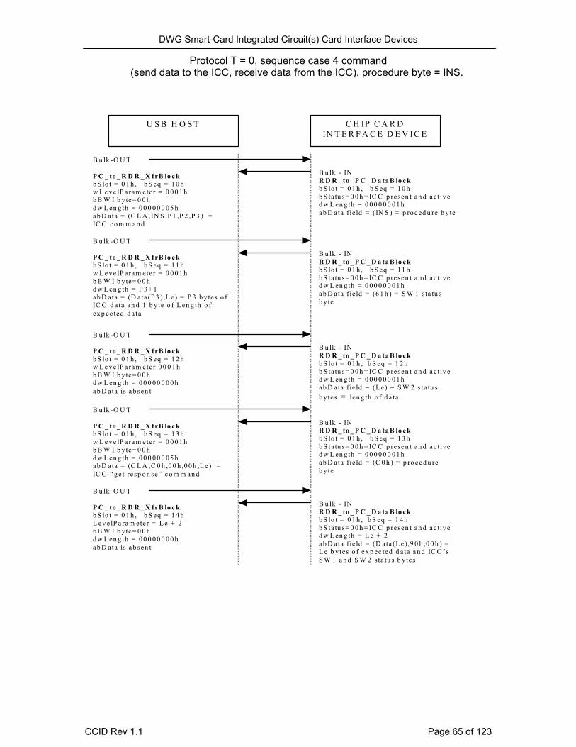
DWG Smart-Card Integrated Circuit(s) Card Interface Devices
Protocol T = 0, sequence case 4 command (send data to the ICC, receive data from the ICC), procedure byte = INS.
U S B H O S T C H IP C A R DIN T E R F A C E D E V IC E
B u lk -O U T
P C _ to _ R D R _ X frB lo c kb S lo t = 0 1 h , b S eq = 1 0 hw L e v e lP a ra m ete r = 0 0 0 1 hb B W I b y te= 0 0 hd w L en g th = 0 0 0 0 0 0 0 5 ha b D ata = (C L A ,IN S ,P 1 ,P 2 ,P 3 ) =IC C c o m m an d
B u lk - INR D R _ to _ P C _ D a ta B lo c kb S lo t = 0 1 h , b S eq = 1 0 hb S ta tu s= 0 0 h = IC C p re sen t an d a c tiv ed w L en g th = 0 0 0 0 0 0 0 1 ha b D ata f ie ld = (IN S ) = p ro c ed u re b y te
B u lk -O U T
P C _ to _ R D R _ X frB lo c kb S lo t = 0 1 h , b S eq = 1 1 hw L e v e lP a ra m ete r = 0 0 0 1 hb B W I b y te= 0 0 hd w L en g th = P 3 + 1a b D ata = (D a ta (P 3 ),L e) = P 3 b y tes o fIC C d a ta an d 1 b y te o f L en g th o fex p ec ted d a ta
B u lk - INR D R _ to _ P C _ D a ta B lo c kb S lo t = 0 1 h , b S eq = 1 1 hb S ta tu s= 0 0 h = IC C p re sen t an d a c tiv ed w L en g th = 0 0 0 0 0 0 0 1 ha b D ata f ie ld = (6 1 h ) = S W 1 sta tu sb y te
B u lk - INR D R _ to _ P C _ D a ta B lo c kb S lo t = 0 1 h , b S eq = 1 2 hb S ta tu s= 0 0 h = IC C p re sen t an d a c tiv ed w L en g th = 0 0 0 0 0 0 0 1 ha b D ata f ie ld = (L e) = S W 2 s ta tu sb y tes = len g th o f d a ta
B u lk -O U T
P C _ to _ R D R _ X frB lo c kb S lo t = 0 1 h , b S eq = 1 2 hw L e v e lP a ra m ete r 0 0 0 1 hb B W I b y te= 0 0 hd w L en g th = 0 0 0 0 0 0 0 0 ha b D ata is a b sen t
B u lk -O U T
P C _ to _ R D R _ X frB lo c kb S lo t = 0 1 h , b S eq = 1 4 hL e v e lP a ra m ete r = L e + 2b B W I b y te= 0 0 hd w L en g th = 0 0 0 0 0 0 0 0 ha b D ata is a b sen t
B u lk -O U T
P C _ to _ R D R _ X frB lo c kb S lo t = 0 1 h , b S eq = 1 3 hw L e v e lP a ra m ete r = 0 0 0 1 hb B W I b y te= 0 0 hd w L en g th = 0 0 0 0 0 0 0 5 ha b D ata = (C L A ,C 0 h ,0 0 h ,0 0 h ,L e ) =IC C “g e t re sp o n se” c o m m a n d
B u lk - INR D R _ to _ P C _ D a ta B lo c kb S lo t = 0 1 h , b S eq = 1 3 hb S ta tu s= 0 0 h = IC C p re sen t an d a c tiv ed w L en g th = 0 0 0 0 0 0 0 1 ha b D ata f ie ld = (C 0 h ) = p ro c ed u reb y te
B u lk - INR D R _ to _ P C _ D a ta B lo c kb S lo t = 0 1 h , b S eq = 1 4 hb S ta tu s= 0 0 h = IC C p re sen t an d a c tiv ed w L en g th = L e + 2a b D ata f ie ld = (D a ta (L e),9 0 h ,0 0 h ) =L e b y tes o f e x p ec ted d a ta a n d IC C ’sS W 1 a n d S W 2 sta tu s b y tes
CCID Rev 1.1 Page 65 of 123
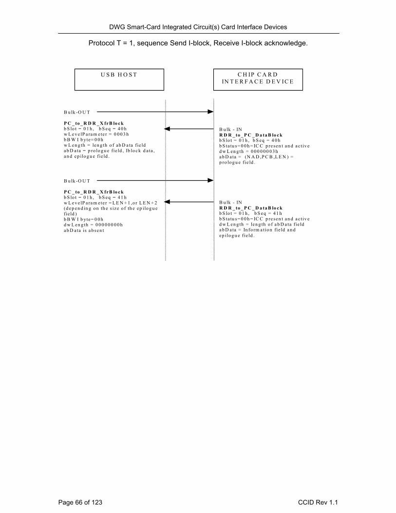
DWG Smart-Card Integrated Circuit(s) Card Interface Devices
Protocol T = 1, sequence Send I-block, Receive I-block acknowledge.
U S B H O S T C H IP C A R D IN T E R F A C E D E V IC E
B u lk -O U T P C _ to _ R D R _ X frB lo c k b S lo t = 0 1 h , b S eq = 4 0 h w L e v e lP a ra m ete r = 0 0 0 3 h b B W I b y te= 0 0 h w L en g th = len g th o f ab D a ta f ie ld a b D ata = p ro lo g u e fie ld , Ib lo c k d a ta , a n d ep ilo g u e f ie ld .
B u lk - IN R D R _ to _ P C _ D a ta B lo c k b S lo t = 0 1 h , b S eq = 4 0 h b S ta tu s= 0 0 h = IC C p re sen t an d a c tiv e d w L en g th = 0 0 0 0 0 0 0 3 h a b D ata = (N A D ,P C B ,L E N ) = p ro lo g u e f ie ld .
B u lk -O U T P C _ to _ R D R _ X frB lo c k b S lo t = 0 1 h , b S eq = 4 1 h w L e v e lP a ra m ete r = L E N + 1 ,o r L E N + 2 (d ep en d in g on th e s ize o f th e ep ilo g u e fie ld ) b B W I b y te= 0 0 h d w L en g th = 0 0 0 0 0 0 0 0 h a b D ata is a b sen t
B u lk - IN R D R _ to _ P C _ D a ta B lo c k b S lo t = 0 1 h , b S eq = 4 1 h b S ta tu s= 0 0 h = IC C p re sen t an d a c tiv e d w L en g th = len g th o f a b D a ta f ie ld a b D ata = In fo rm a tio n fie ld a n d ep ilo g u e fie ld .
Page 66 of 123 CCID Rev 1.1
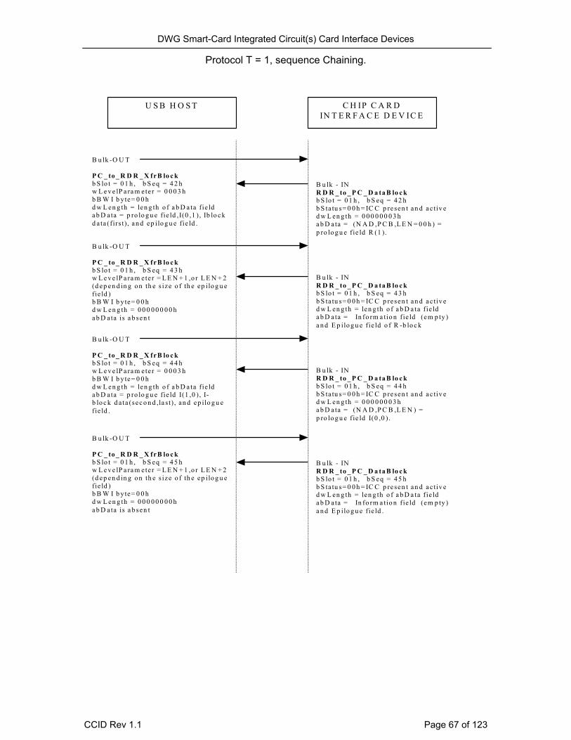
DWG Smart-Card Integrated Circuit(s) Card Interface Devices
Protocol T = 1, sequence Chaining.
U S B H O S T C H IP C A R DIN T E R F A C E D E V IC E
B u lk -O U T
P C _ to _ R D R _ X frB lo c kb S lo t = 0 1 h , b S eq = 4 2 hw L e v e lP a ra m ete r = 0 0 0 3 hb B W I b y te= 0 0 hd w L en g th = len g th o f a b D a ta fie lda b D ata = p ro lo g u e fie ld ,I(0 ,1 ), Ib lo c kd a ta (firs t) , an d ep ilo g u e fie ld .
B u lk - INR D R _ to _ P C _ D a ta B lo c kb S lo t = 0 1 h , b S eq = 4 2 hb S ta tu s= 0 0 h = IC C p re sen t an d a c tiv ed w L en g th = 0 0 0 0 0 0 0 3 ha b D ata = (N A D ,P C B ,L E N = 0 0 h ) =p ro lo g u e f ie ld R (1 ).
B u lk -O U T
P C _ to _ R D R _ X frB lo c kb S lo t = 0 1 h , b S eq = 4 3 hw L e v e lP a ra m ete r = L E N + 1 ,o r L E N + 2(d ep en d in g on th e s ize o f th e ep ilo g u efie ld )b B W I b y te= 0 0 hd w L en g th = 0 0 0 0 0 0 0 0 ha b D ata is a b sen t
B u lk - INR D R _ to _ P C _ D a ta B lo c kb S lo t = 0 1 h , b S eq = 4 3 hb S ta tu s= 0 0 h = IC C p re sen t an d a c tiv ed w L en g th = len g th o f a b D a ta f ie lda b D ata = In fo rm a tio n f ie ld (em p ty )a n d E p ilo g u e f ie ld o f R -b lo c k
B u lk -O U T
P C _ to _ R D R _ X frB lo c kb S lo t = 0 1 h , b S eq = 4 4 hw L e v e lP a ra m ete r = 0 0 0 3 hb B W I b y te= 0 0 hd w L en g th = len g th o f a b D a ta fie lda b D ata = p ro lo g u e fie ld I(1 ,0 ), I-b lo c k d a ta (sec o n d ,la st) , an d ep ilo g u efie ld .
B u lk - INR D R _ to _ P C _ D a ta B lo c kb S lo t = 0 1 h , b S eq = 4 4 hb S ta tu s= 0 0 h = IC C p re sen t an d a c tiv ed w L en g th = 0 0 0 0 0 0 0 3 ha b D ata = (N A D ,P C B ,L E N ) =p ro lo g u e f ie ld I(0 ,0 ) .
B u lk -O U T
P C _ to _ R D R _ X frB lo c kb S lo t = 0 1 h , b S eq = 4 5 hw L e v e lP a ra m ete r = L E N + 1 ,o r L E N + 2(d ep en d in g on th e s ize o f th e ep ilo g u efie ld )b B W I b y te= 0 0 hd w L en g th = 0 0 0 0 0 0 0 0 ha b D ata is a b sen t
B u lk - INR D R _ to _ P C _ D a ta B lo c kb S lo t = 0 1 h , b S eq = 4 5 hb S ta tu s= 0 0 h = IC C p re sen t an d a c tiv ed w L en g th = len g th o f a b D a ta f ie lda b D ata = In fo rm a tio n f ie ld (em p ty )a n d E p ilo g u e f ie ld .
CCID Rev 1.1 Page 67 of 123

DWG Smart-Card Integrated Circuit(s) Card Interface Devices
Protocol T = 1, sequence Waiting Time Extension.
U S B H O S T C H IP C A R DIN T E R F A C E D E V IC E
B u lk -O U T
P C _ to _ R D R _ X frB lo c kb S lo t = 0 1 h , b S eq = 4 6 hw L e v e lP a ra m ete r = 0 0 0 3 hb B W I b y te= 0 0 hd w L en g th = len g th o f a b D a ta fie lda b D ata = p ro lo g u e fie ld , I(0 ,0 ),Ib lo c k d a ta , an d ep ilo g u e f ie ld .
B u lk - INR D R _ to _ P C _ D a ta B lo c kb S lo t = 0 1 h , b S eq = 4 6 hb S ta tu s= 0 0 h = IC C p re sen t an d a c tiv ed w L en g th = 0 0 0 0 0 0 0 3 ha b D ata = (N A D ,P C B ,L E N = 1 ) =p ro lo g u e f ie ld S (W T X req u es t) .
B u lk -O U T
P C _ to _ R D R _ X frB lo c kb S lo t = 0 1 h , b S eq = 4 7 hw L e v e lP a ra m ete r = L E N + 1 ,o r L E N + 2(d ep en d in g on th e s ize o f th e ep ilo g u efie ld ) b B W I b y te= 0 0 hd w L en g th = 0 0 0 0 0 0 0 0 ha b D ata is a b sen t
B u lk - INR D R _ to _ P C _ D a ta B lo c kb S lo t = 0 1 h , b S eq = 4 7 hb S ta tu s= 0 0 h = IC C p re sen t an d a c tiv ed w L en g th = len g th o f a b D a ta f ie lda b D ata = In fo rm a tio n fie ld (1 b y te )a n d E p ilo g u e f ie ld o f S B lo c k
B u lk -O U T
P C _ to _ R D R _ X frB lo c kb S lo t = 0 1 h , b S eq = 4 8 hw L e v e lP a ra m ete r = 0 0 0 3 hb B W I b y te= Z Zd w L en g th = len g th o f a b D a ta fie lda b D ata = p ro lo g u e fie ld S (W T Xresp o n se) , In fo rm a tio n f ie ld (1 b y te ) ,a n d ep ilo g u e f ie ld
B u lk - INR D R _ to _ P C _ D a ta B lo c kb S lo t = 0 1 h , b S eq = 4 8 hb S ta tu s= 0 0 h = IC C p re sen t an d a c tiv ed w L en g th = 0 0 0 0 0 0 0 3 ha b D ata = (N A D ,P C B ,L E N ) =p ro lo g u e f ie ld I(0 ,0 ) .
B u lk -O U T
P C _ to _ R D R _ X frB lo c kb S lo t = 0 1 h , b S eq = 4 9 hw L e v e lP a ra m ete r = L E N + 1 ,o r L E N + 2(d ep en d in g on th e s ize o f th e ep ilo g u efie ld )b B W I b y te= 0 0 hd w L en g th = 0 0 0 0 0 0 0 0 ha b D ata is a b sen t
B u lk - INR D R _ to _ P C _ D a ta B lo c kb S lo t = 0 1 h , b S eq = 4 9 hb S ta tu s= 0 0 h = IC C p re sen t an d a c tiv ed w L en g th = len g th o f a b D a ta f ie lda b D ata = In fo rm a tio n f ie ld (em p ty )a n d E p ilo g u e f ie ld .
.
.w a it u p to an
ex tra Z Z B W Ttim es b e fo ret im in g ou t
.
Page 68 of 123 CCID Rev 1.1

DWG Smart-Card Integrated Circuit(s) Card Interface Devices
7.3 APDU Level These sequences show exchanges with an ICC in slot bSlot=01h. This is the “second” slot of a multiple slot CCID. Exchanges with an ICC in the “first” slot of a multiple slot CCID or in the only slot of a single slot CCID would require using bSlot=00h.
Buffer length = dwMaxCCIDMessageLength - header length (10).
Protocol T = 0, sequence case 1 command.
U S B H O S T C H IP C A R D IN T E R F A C ED E V IC E
B u lk -O U T
P C _ to _ R D R _ X frB lo c kb S lo t = 0 1 h , b S eq = 0 A hw L e v e lP a ra m ete r = 0 0 0 0 hb B W I b y te= 0 0 hd w L en g th = 0 0 0 0 0 0 0 4 ha b D ata = (C L A ,IN S ,P 1 ,P 2 ) = IC Cc o m m a n d
B u lk - INR D R _ to _ P C _ D a ta B lo c kb S lo t = 0 1 h , b S eq = 0 A hb S ta tu s= 0 0 h = IC C p resen t an d a c tiv ed w L en g th = 0 0 0 0 0 0 0 2 ha b D ata = (9 0 h ,0 0 h ) = S W 1 a n d S W 2sta tu s b y tes .
C L A ,IN S ,P 1 ,P 2 ,0 0
9 0 ,0 0
IC C
CCID Rev 1.1 Page 69 of 123

DWG Smart-Card Integrated Circuit(s) Card Interface Devices
Protocol T = 0, sequence case 2 command (expect data from the ICC) with the length not accepted by the ICC,
buffer length >= APDU length.
U S B H O S T C H IP C A R D IN T E R F A C ED E V IC E
B u lk -O U T
P C _ to _ R D R _ X frB lo c kb S lo t = 0 1 h , b S eq = 0 B hw L e v e lP a ra m ete r = 0 0 0 0 hb B W I b y te= 0 0 hd w L en g th = 0 0 0 0 0 0 0 5 ha b D ata = (C L A ,IN S ,P 1 ,P 2 ,P 3 ) =IC C c o m m an d
6 C ,X X
C L A ,IN S ,P 1 ,P 2 ,P 3
B u lk - INR D R _ to _ P C _ D a ta B lo c kb S lo t = 0 1 h , b S eq = 0 B hb S ta tu s= 0 0 h = IC C p resen t an d a c t iv ed w L en g th = X X + 2a b D ata = (D a ta (X X ),9 0 h ,0 0 h ) = IC C ’sd a ta a n d S W 1 a n d S W 2 sta tu s b y tes .
IC C
C L A ,IN S ,P 1 ,P 2 ,X X
IN S ,D a ta 1 ,D a ta2 ,…D a ta X X ,9 0 ,0 0
Page 70 of 123 CCID Rev 1.1
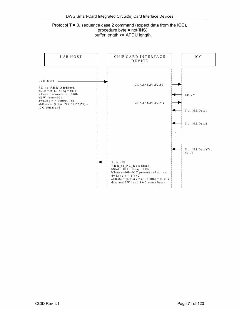
DWG Smart-Card Integrated Circuit(s) Card Interface Devices
Protocol T = 0, sequence case 2 command (expect data from the ICC), procedure byte = not(INS),
buffer length >= APDU length.
U S B H O S T C H IP C A R D IN T E R F A C ED E V IC E
B u lk -O U T
P C _ to _ R D R _ X frB lo c kb S lo t = 0 1 h , b S eq = 0 C hw L e v e lP a ra m ete r = 0 0 0 0 hb B W I b y te= 0 0 hd w L en g th = 0 0 0 0 0 0 0 5 ha b D ata = (C L A ,IN S ,P 1 ,P 2 ,P 3 ) =IC C c o m m an d
6 C ,Y Y
C L A ,IN S ,P 1 ,P 2 ,P 3
B u lk - INR D R _ to _ P C _ D a ta B lo c kb S lo t = 0 1 h , b S eq = 0 C hb S ta tu s= 0 0 h = IC C p resen t an d a c t iv ed w L en g th = Y Y + 2a b D ata = (D a ta (Y Y ),9 0 h ,0 0 h ) = IC C ’sd a ta a n d S W 1 a n d S W 2 sta tu s b y tes
IC C
C L A ,IN S ,P 1 ,P 2 ,Y Y
N o t IN S ,D a ta 1
N o t IN S ,D a ta 2
N o t IN S ,D a ta Y Y ,9 0 ,0 0
.
.
.
CCID Rev 1.1 Page 71 of 123
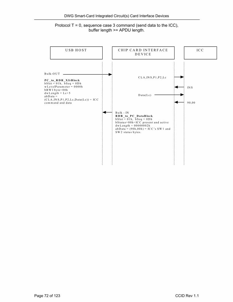
DWG Smart-Card Integrated Circuit(s) Card Interface Devices
Protocol T = 0, sequence case 3 command (send data to the ICC), buffer length >= APDU length.
U S B H O S T C H IP C A R D IN T E R F A C ED E V IC E
B u lk -O U T
P C _ to _ R D R _ X frB lo c kb S lo t = 0 1 h , b S eq = 0 D hw L e v e lP a ra m ete r = 0 0 0 0 hb B W I b y te= 0 0 hd w L en g th = L c + 5a b D ata =(C L A ,IN S ,P 1 ,P 2 ,L c ,D a ta (L c )) = IC Cc o m m a n d a n d d a ta
IN S
C L A ,IN S ,P 1 ,P 2 ,L c
B u lk - INR D R _ to _ P C _ D a ta B lo c kb S lo t = 0 1 h , b S eq = 0 D hb S ta tu s= 0 0 h = IC C p resen t an d a c t iv ed w L en g th = 0 0 0 0 0 0 0 2 ha b D ata = (9 0 h ,0 0 h ) = IC C ’s S W 1 a n dS W 2 s ta tu s b y tes .
IC C
D a ta (L c )
9 0 ,0 0
Page 72 of 123 CCID Rev 1.1
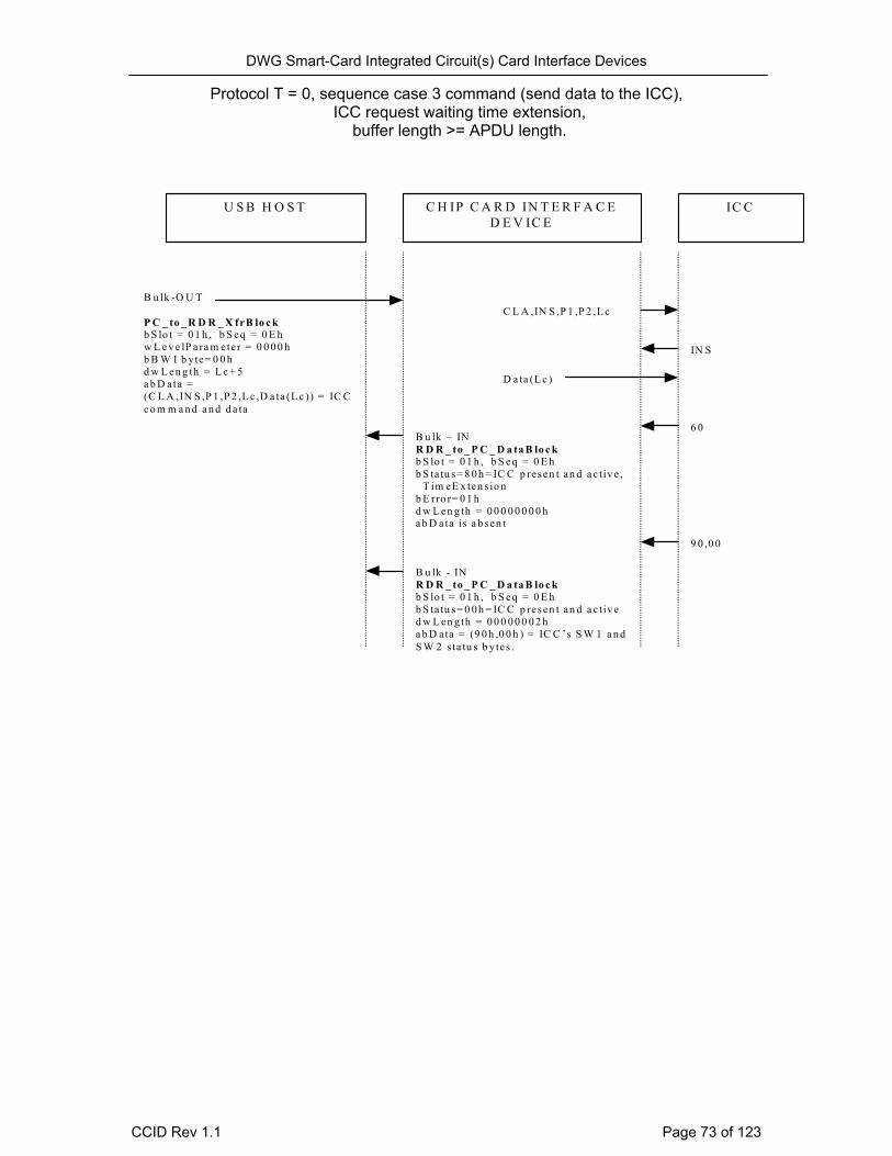
DWG Smart-Card Integrated Circuit(s) Card Interface Devices
Protocol T = 0, sequence case 3 command (send data to the ICC), ICC request waiting time extension,
buffer length >= APDU length.
U S B H O S T C H IP C A R D IN T E R F A C ED E V IC E
B u lk -O U T
P C _ to _ R D R _ X frB lo c kb S lo t = 0 1 h , b S eq = 0 E hw L e v e lP a ra m ete r = 0 0 0 0 hb B W I b y te= 0 0 hd w L en g th = L c + 5a b D ata =(C L A ,IN S ,P 1 ,P 2 ,L c ,D a ta (L c )) = IC Cc o m m a n d a n d d a ta
IN S
C L A ,IN S ,P 1 ,P 2 ,L c
B u lk - INR D R _ to _ P C _ D a ta B lo c kb S lo t = 0 1 h , b S eq = 0 E hb S ta tu s= 0 0 h = IC C p resen t an d a c t iv ed w L en g th = 0 0 0 0 0 0 0 2 ha b D ata = (9 0 h ,0 0 h ) = IC C ’s S W 1 a n dS W 2 s ta tu s b y tes .
IC C
D a ta (L c )
9 0 ,0 0
6 0B u lk – INR D R _ to _ P C _ D a ta B lo c kb S lo t = 0 1 h , b S eq = 0 E hb S ta tu s= 8 0 h = IC C p resen t an d a c t iv e , T im eE x ten s io nb E rro r= 0 1 hd w L en g th = 0 0 0 0 0 0 0 0 ha b D ata is a b sen t
CCID Rev 1.1 Page 73 of 123
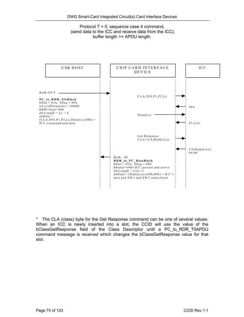
DWG Smart-Card Integrated Circuit(s) Card Interface Devices
Protocol T = 0, sequence case 4 command, (send data to the ICC and receive data from the ICC),
buffer length >= APDU length.
U S B H O S T C H IP C A R D IN T E R F A C ED E V IC E
B u lk -O U T
P C _ to _ R D R _ X frB lo c kb S lo t = 0 1 h , b S eq = 0 F hw L e v e lP a ra m ete r = 0 0 0 0 hb B W I b y te= 0 0 hd w L en g th = L c + 6a b D ata =(C L A ,IN S ,P 1 ,P 2 ,L c ,D a ta (L c ),0 0 h ) =IC C c o m m an d an d d a ta
IN S
C L A ,IN S ,P 1 ,P 2 ,L c
B u lk - INR D R _ to _ P C _ D a ta B lo c kb S lo t = 0 1 h , b S eq = 0 F hb S ta tu s= 0 0 h = IC C p resen t an d a c t iv ed w L en g th = L ic c + 2a b D ata = (D a ta (L ic c ) ,9 0 h ,0 0 h ) = IC C ’sd a ta a n d S W 1 a n d S W 2 sta tu s b y tes
IC C
D a ta (L c )
6 1 ,L ic c
G et R esp o n seC L A * ,C 0 ,0 0 ,0 0 ,L ic c
C 0 ,D a ta (L ic c ) ,9 0 ,0 0
* The CLA (class) byte for the Get Response command can be one of several values. When an ICC is newly inserted into a slot, the CCID will use the value of the bClassGetResponse field of the Class Descriptor until a PC_to_RDR_T0APDU command message is received which changes the bClassGetResponse value for that slot.
Page 74 of 123 CCID Rev 1.1
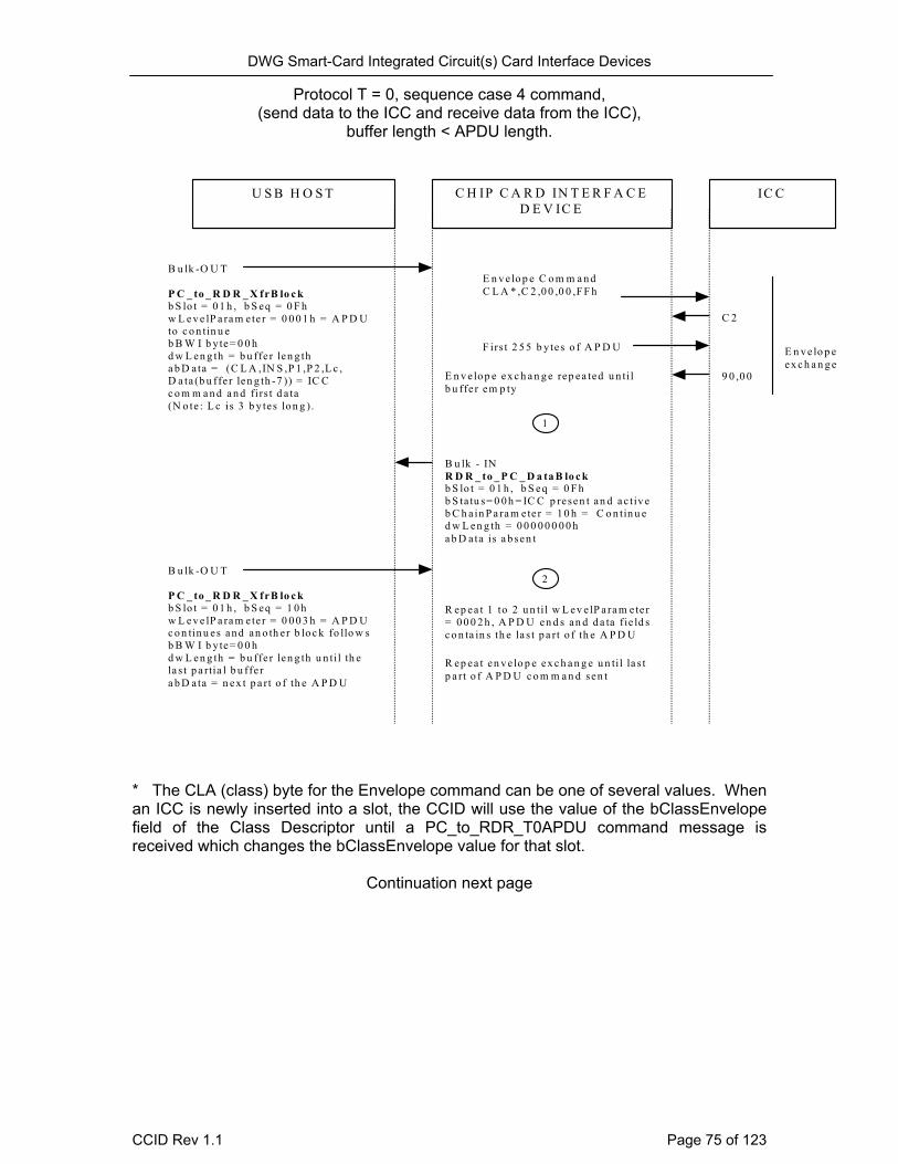
DWG Smart-Card Integrated Circuit(s) Card Interface Devices
Protocol T = 0, sequence case 4 command, (send data to the ICC and receive data from the ICC),
buffer length < APDU length.
U S B H O S T C H IP C A R D IN T E R F A C E D E V IC E
B u lk -O U T P C _ to _ R D R _ X frB lo c k b S lo t = 0 1 h , b S eq = 0 F h w L e v e lP a ra m ete r = 0 0 0 1 h = A P D U to c o n tin u e b B W I b y te= 0 0 h d w L en g th = b u ffe r len g th a b D ata = (C L A ,IN S ,P 1 ,P 2 ,L c , D a ta (b u ffe r len g th -7 )) = IC C c o m m a n d a n d firs t d a ta (N o te : L c is 3 b y tes lo n g ).
C 2
E n v e lo p e C o m m a n d C L A * ,C 2 ,0 0 ,0 0 ,F F h
B u lk - IN R D R _ to _ P C _ D a ta B lo c k b S lo t = 0 1 h , b S eq = 0 F h b S ta tu s= 0 0 h = IC C p resen t an d a c t iv e b C h a in P a ra m ete r = 1 0 h = C o n tin u e d w L en g th = 0 0 0 0 0 0 0 0 h a b D ata is a b sen t
IC C
F irs t 2 5 5 b y tes o f A P D U
9 0 ,0 0
E n v e lo p e ex c h a n g e
E n v e lo p e ex c h a n g e rep ea ted u n ti l b u ffe r em p ty
1
B u lk -O U T P C _ to _ R D R _ X frB lo c k b S lo t = 0 1 h , b S eq = 1 0 h w L e v e lP a ra m ete r = 0 0 0 3 h = A P D U c o n tin u es an d an o th er b lo c k fo llo w s b B W I b y te= 0 0 h d w L en g th = b u ffe r len g th u n ti l th e la s t p a rtia l b u ffe r a b D ata = n ex t p a rt o f th e A P D U
2
R ep ea t 1 to 2 u n til w L ev e lP a ra m ete r = 0 0 0 2 h , A P D U en d s an d d a ta f ie ld s c o n ta in s th e la s t p a rt o f th e A P D U
R ep ea t en v e lo p e ex c h a n g e u n til la s t p a rt o f A P D U c o m m a n d sen t
* The CLA (class) byte for the Envelope command can be one of several values. When an ICC is newly inserted into a slot, the CCID will use the value of the bClassEnvelope field of the Class Descriptor until a PC_to_RDR_T0APDU command message is received which changes the bClassEnvelope value for that slot.
Continuation next page
CCID Rev 1.1 Page 75 of 123
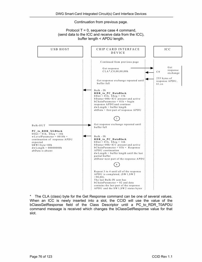
DWG Smart-Card Integrated Circuit(s) Card Interface Devices
Continuation from previous page.
Protocol T = 0, sequence case 4 command, (send data to the ICC and receive data from the ICC),
buffer length < APDU length.
U S B H O S T C H IP C A R D IN T E R F A C ED E V IC E
C 0G et resp o n seC L A * ,C 0 ,0 0 ,0 0 ,0 0 h
B u lk - INR D R _ to _ P C _ D a ta B lo c kb S lo t = 0 1 h , b S eq = 1 5 hb S ta tu s= 0 0 h = IC C p resen t an d a c t iv eb C h a in P a ra m ete r = 0 1 h = b eg inresp o n se A P D U a n d c o n tin u ed w L en g th = b u ffe r len g tha b D ata = firs t p a rt o f re sp o n se A P D U
IC C
2 5 5 b y tes o fresp o n se A P D U ,6 1 ,x x
G etresp o n seex c h a n g e
G et resp o n se ex c h a n g e rep ea ted u n tilb u ffe r fu ll
3
B u lk -O U T
P C _ to _ R D R _ X frB lo c kb S lo t = 0 1 h , b S eq = 1 6 hw L e v e lP a ra m ete r = 0 0 1 0 h =c o n tin u a tion o f re sp o n se A P D Uex p ec tedb B W I b y te= 0 0 hd w L en g th = 0 0 0 0 0 0 0 0 ha b D ata is a b sen t
4
R ep ea t 3 to 4 u n til a ll o f th e resp o n seA P D U is c o m p le ted , (S W 1 ,S W 2= 9 0 ,0 0 ).T h e la s t B u lk -IN sen t h a sb C h a in P a ra m ete r = 0 2 an d d a tac o n ta in s th e la s t p a rt o f th e resp o n seA P D U a n d th e S W 1 ,S W 2 s ta tu s b y tes
C o n tin u ed fro m p rev io u s p a g e
G et resp o n se ex c h a n g e rep ea ted u n tilb u ffe r fu ll
B u lk - INR D R _ to _ P C _ D a ta B lo c kb S lo t = 0 1 h , b S eq = 1 6 hb S ta tu s= 0 0 h = IC C p resen t an d a c t iv eb C h a in P a ra m ete r = 0 3 h = R esp on seA P D U c o n tin u a tiond w L en g th = b u ffe r len g th u n til th e la s tp a rtia l b u ffe ra b D ata= n ex t p a rt o f th e resp o n se A P D U
* The CLA (class) byte for the Get Response command can be one of several values. When an ICC is newly inserted into a slot, the CCID will use the value of the bClassGetResponse field of the Class Descriptor until a PC_to_RDR_T0APDU command message is received which changes the bClassGetResponse value for that slot.
Page 76 of 123 CCID Rev 1.1
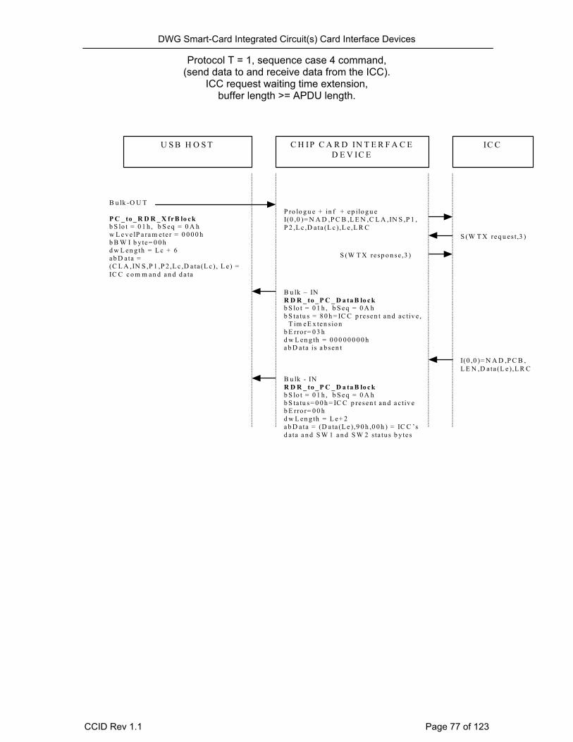
DWG Smart-Card Integrated Circuit(s) Card Interface Devices
Protocol T = 1, sequence case 4 command, (send data to and receive data from the ICC).
ICC request waiting time extension, buffer length >= APDU length.
U S B H O S T C H IP C A R D IN T E R F A C ED E V IC E
B u lk -O U T
P C _ to _ R D R _ X frB lo c kb S lo t = 0 1 h , b S eq = 0 A hw L e v e lP a ra m ete r = 0 0 0 0 hb B W I b y te= 0 0 hd w L en g th = L c + 6a b D ata =(C L A ,IN S ,P 1 ,P 2 ,L c ,D a ta (L c ), L e) =IC C c o m m an d an d d a ta
S (W T X req u es t,3 )
P ro lo g u e + in f + ep ilo g u eI(0 ,0 )= N A D ,P C B ,L E N ,C L A ,IN S ,P 1 ,P 2 ,L c ,D a ta (L c ),L e ,L R C
B u lk - INR D R _ to _ P C _ D a ta B lo c kb S lo t = 0 1 h , b S eq = 0 A hb S ta tu s= 0 0 h = IC C p resen t an d a c t iv eb E rro r= 0 0 hd w L en g th = L e+ 2a b D ata = (D a ta (L e ),9 0 h ,0 0 h ) = IC C ’sd a ta a n d S W 1 a n d S W 2 sta tu s b y tes
IC C
S (W T X resp o n se ,3 )
I(0 ,0 )= N A D ,P C B ,L E N ,D a ta (L e),L R C
B u lk – INR D R _ to _ P C _ D a ta B lo c kb S lo t = 0 1 h , b S eq = 0 A hb S ta tu s = 8 0 h = IC C p resen t a n d a c tiv e , T im eE x ten s io nb E rro r= 0 3 hd w L en g th = 0 0 0 0 0 0 0 0 ha b D ata is a b sen t
CCID Rev 1.1 Page 77 of 123
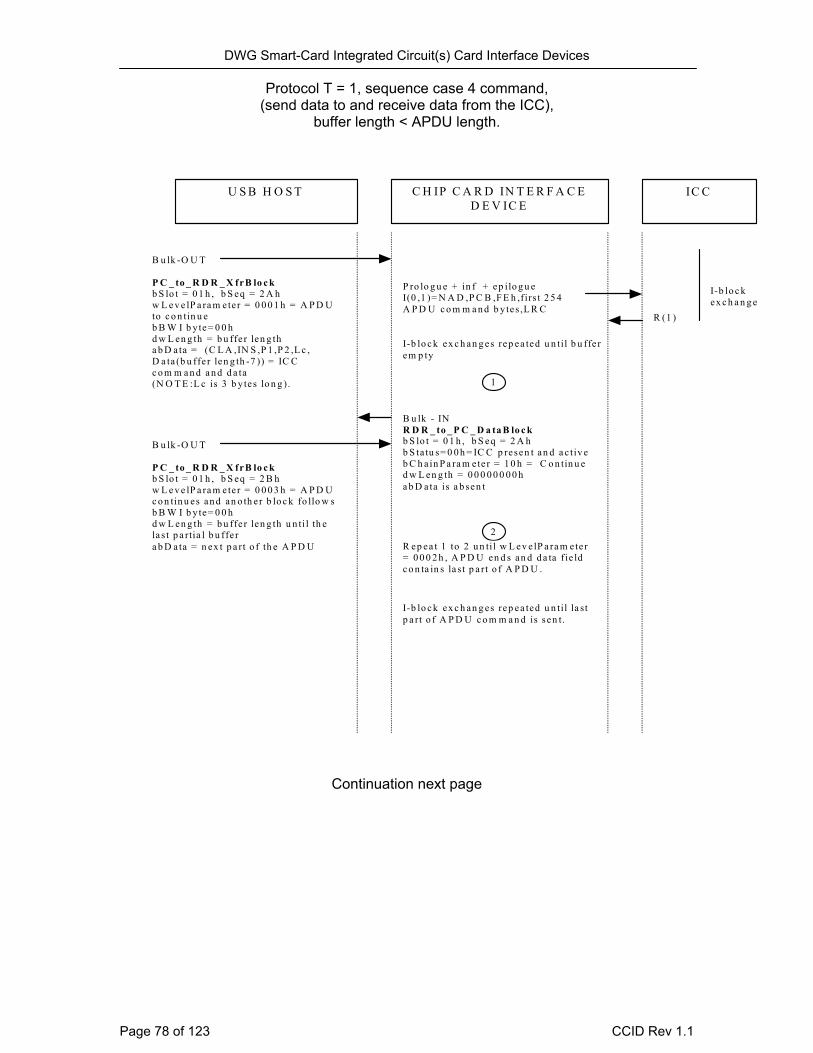
DWG Smart-Card Integrated Circuit(s) Card Interface Devices
Protocol T = 1, sequence case 4 command, (send data to and receive data from the ICC),
buffer length < APDU length.
U S B H O S T C H IP C A R D IN T E R F A C E D E V IC E
R (1 )
P ro lo g u e + in f + ep ilo g u e I(0 ,1 )= N A D ,P C B ,F E h ,f irs t 2 5 4 A P D U c o m m a n d b y tes ,L R C
B u lk - IN R D R _ to _ P C _ D a ta B lo c k b S lo t = 0 1 h , b S eq = 2 A h b S ta tu s= 0 0 h = IC C p resen t an d a c t iv e b C h a in P a ra m ete r = 1 0 h = C o n tin u e d w L en g th = 0 0 0 0 0 0 0 0 h a b D ata is a b sen t
IC C
I-b lo c k ex c h an g es rep ea ted u n til b u ffe r em p ty
I-b lo c k ex c h a n g e
1
B u lk -O U T P C _ to _ R D R _ X frB lo c k b S lo t = 0 1 h , b S eq = 2 B h w L e v e lP a ra m ete r = 0 0 0 3 h = A P D U c o n tin u es an d an o th er b lo c k fo llo w s b B W I b y te= 0 0 h d w L en g th = b u ffe r len g th u n ti l th e la s t p a rtia l b u ffe r a b D ata = n ex t p a rt o f th e A P D U
2R ep ea t 1 to 2 u n til w L ev e lP a ra m ete r = 0 0 0 2 h , A P D U en d s an d d a ta f ie ld c o n ta in s la st p a rt o f A P D U .
I-b lo c k ex c h an g es rep ea ted u n til la st p a rt o f A P D U c o m m a n d is sen t.
B u lk -O U T P C _ to _ R D R _ X frB lo c k b S lo t = 0 1 h , b S eq = 2 A h w L e v e lP a ra m ete r = 0 0 0 1 h = A P D U to c o n tin u e b B W I b y te= 0 0 h d w L en g th = b u ffe r len g th a b D ata = (C L A ,IN S ,P 1 ,P 2 ,L c , D a ta (b u ffe r len g th -7 )) = IC C c o m m a n d a n d d a ta (N O T E :L c is 3 b y tes lo n g ).
Continuation next page
Page 78 of 123 CCID Rev 1.1

DWG Smart-Card Integrated Circuit(s) Card Interface Devices
Continuation from previous page. Protocol T = 1, sequence case 4 command,
(send data to and receive data from the ICC), buffer length < APDU length
U S B H O S T C H IP C A R D IN T E R F A C ED E V IC E
R (1 )
I(0 ,1 )= N A D ,P C B ,F E h ,f irs t 2 5 4A P D U resp o n se b y tes ,L R C
B u lk - INR D R _ to _ P C _ D a ta B lo c kb S lo t = 0 1 h , b S eq = 3 1 hb S ta tu s= 0 0 h = IC C p resen t an d a c t iv eb C h a in P a ra m ete r = 0 1 h = b eg inresp o n se A P D U a n d c on tin u ed w L en g th = b u ffe r len g tha b D ata = firs t p a rt o f re sp o n se A P D U
IC C
I-b lo c k ex c h an g es fro m IC C rep ea tedu n ti l b u ffe r fu ll
I-b lo c kex c h a n g efro m IC C
3
B u lk -O U T
P C _ to _ R D R _ X frB lo c kb S lo t = 0 1 h , b S eq = 3 2 hw L e v e lP a ra m ete r = 0 0 1 0 h =c o n tin u a tion o f re sp o n se A P D U isex p ec tedb B W I b y te= 0 0 hd w L en g th = 0 0 0 0 0 0 0 0 ha b D ata is a b sen t
4
R ep ea t 3 to 4 u n til a ll o f th e resp o n seA P D U is c o m p le ted , I(x ,0 ), th e la s tB u lk -IN sen t h a s th eb C h a in P a ra m ete r = 0 2 h resp o n seA P D U en d , a n d th e d a ta c o n ta in s th ela s t p a rt o f th e resp o n se A P D U a n dth e S W 1 ,S W 2 s ta tu s b y tes
C o n tin u ed fro m p rev io u s p a g e
B u lk - INR D R _ to _ P C _ D a ta B lo c kb S lo t = 0 1 h , b S eq = 3 2 hb S ta tu s= 0 0 h = IC C p resen t an d a c t iv eb C h a in P a ra m ete r = 0 3 h = resp on seA P D U c o n tin u a tiond w L en g th = b u ffe r len g th u n til th e la s tp a rtia l b u ffe ra b D ata= n ex t p a rt o f th e resp o n se A P D U
I-b lo c k ex c h an g es fro m IC C rep ea tedu n ti l b u ffe r fu ll
CCID Rev 1.1 Page 79 of 123
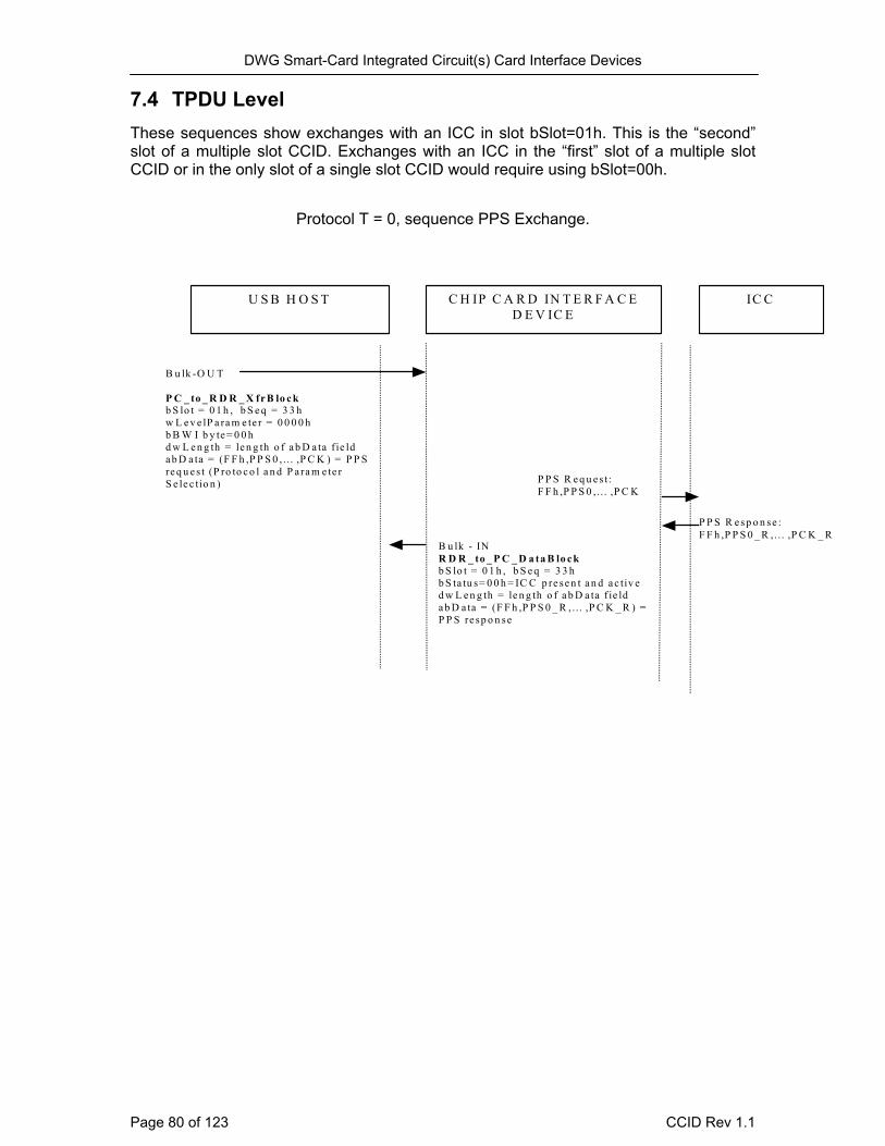
DWG Smart-Card Integrated Circuit(s) Card Interface Devices 7.4 TPDU Level These sequences show exchanges with an ICC in slot bSlot=01h. This is the “second” slot of a multiple slot CCID. Exchanges with an ICC in the “first” slot of a multiple slot CCID or in the only slot of a single slot CCID would require using bSlot=00h.
Protocol T = 0, sequence PPS Exchange.
U S B H O S T C H IP C A R D IN T E R F A C E D E V IC E
P P S R e sp o n se : F F h ,P P S 0 _ R ,… ,P C K _ R
P P S R e q u e s t: F F h ,P P S 0 ,… ,P C K
B u lk - IN R D R _ to _ P C _ D a ta B lo c k b S lo t = 0 1 h , b S e q = 3 3 h b S ta tu s= 0 0 h = IC C p re se n t a n d a c tiv e d w L e n g th = le n g th o f a b D a ta f ie ld a b D a ta = (F F h ,P P S 0 _ R ,… ,P C K _ R ) = P P S re sp o n se
IC C
B u lk -O U T P C _ to _ R D R _ X fr B lo c k b S lo t = 0 1 h , b S e q = 3 3 h w L e v e lP a ra m e te r = 0 0 0 0 h b B W I b y te = 0 0 h d w L e n g th = le n g th o f a b D a ta f ie ld a b D a ta = (F F h ,P P S 0 ,… ,P C K ) = P P S re q u e s t (P ro to c o l a n d P a ra m e te r S e le c tio n )
Page 80 of 123 CCID Rev 1.1
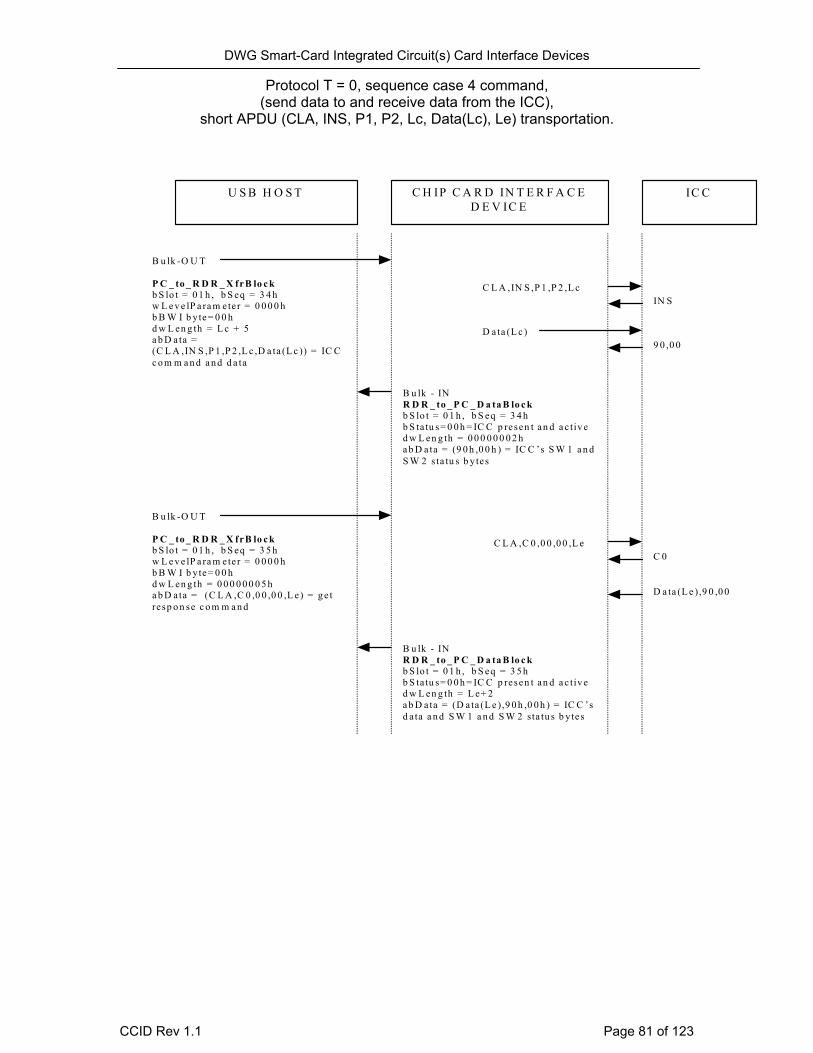
DWG Smart-Card Integrated Circuit(s) Card Interface Devices
Protocol T = 0, sequence case 4 command, (send data to and receive data from the ICC),
short APDU (CLA, INS, P1, P2, Lc, Data(Lc), Le) transportation.
U S B H O S T C H IP C A R D IN T E R F A C ED E V IC E
IN SC L A ,IN S ,P 1 ,P 2 ,L c
B u lk - INR D R _ to _ P C _ D a ta B lo c kb S lo t = 0 1 h , b S eq = 3 4 hb S ta tu s= 0 0 h = IC C p resen t an d a c t iv ed w L en g th = 0 0 0 0 0 0 0 2 ha b D ata = (9 0 h ,0 0 h ) = IC C ’s S W 1 a n dS W 2 s ta tu s b y tes
IC C
B u lk -O U T
P C _ to _ R D R _ X frB lo c kb S lo t = 0 1 h , b S eq = 3 4 hw L e v e lP a ra m ete r = 0 0 0 0 hb B W I b y te= 0 0 hd w L en g th = L c + 5a b D ata =(C L A ,IN S ,P 1 ,P 2 ,L c ,D a ta (L c )) = IC Cc o m m a n d a n d d a ta
9 0 ,0 0D a ta (L c )
B u lk - INR D R _ to _ P C _ D a ta B lo c kb S lo t = 0 1 h , b S eq = 3 5 hb S ta tu s= 0 0 h = IC C p resen t an d a c t iv ed w L en g th = L e+ 2a b D ata = (D a ta (L e ),9 0 h ,0 0 h ) = IC C ’sd a ta a n d S W 1 a n d S W 2 sta tu s b y tes
B u lk -O U T
P C _ to _ R D R _ X frB lo c kb S lo t = 0 1 h , b S eq = 3 5 hw L e v e lP a ra m ete r = 0 0 0 0 hb B W I b y te= 0 0 hd w L en g th = 0 0 0 0 0 0 0 5 ha b D ata = (C L A ,C 0 ,0 0 ,0 0 ,L e) = g e tresp o n se c o m m a n d
C L A ,C 0 ,0 0 ,0 0 ,L eC 0
D a ta (L e ),9 0 ,0 0
CCID Rev 1.1 Page 81 of 123
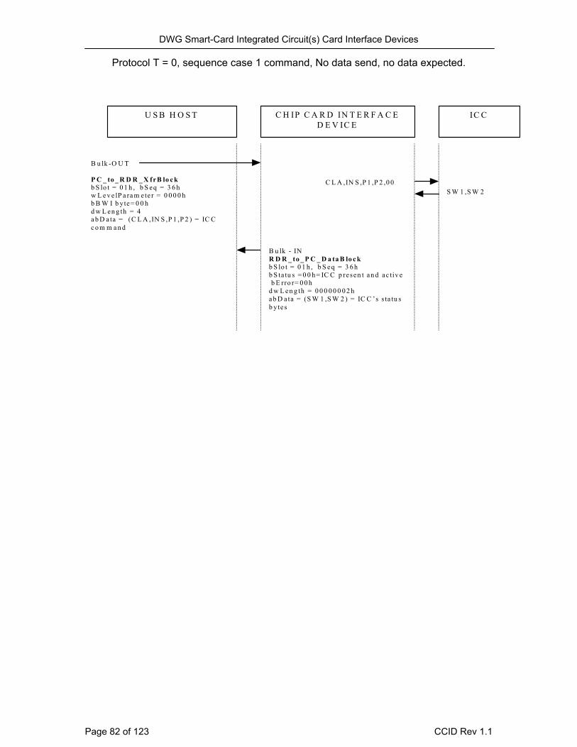
DWG Smart-Card Integrated Circuit(s) Card Interface Devices
Protocol T = 0, sequence case 1 command, No data send, no data expected.
U S B H O S T C H IP C A R D IN T E R F A C ED E V IC E
S W 1 ,S W 2C L A ,IN S ,P 1 ,P 2 ,0 0
B u lk - INR D R _ to _ P C _ D a ta B lo c kb S lo t = 0 1 h , b S eq = 3 6 hb S ta tu s = 0 0 h = IC C p resen t an d ac tiv e b E rro r= 0 0 hd w L en g th = 0 0 0 0 0 0 0 2 ha b D ata = (S W 1 ,S W 2 ) = IC C ’s s ta tu sb y tes
IC C
B u lk -O U T
P C _ to _ R D R _ X frB lo c kb S lo t = 0 1 h , b S eq = 3 6 hw L e v e lP a ra m ete r = 0 0 0 0 hb B W I b y te= 0 0 hd w L en g th = 4a b D ata = (C L A ,IN S ,P 1 ,P 2 ) = IC Cc o m m a n d
Page 82 of 123 CCID Rev 1.1
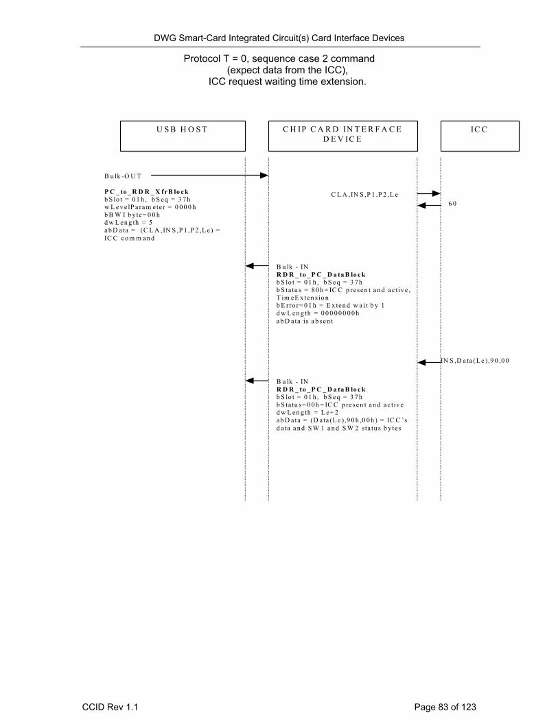
DWG Smart-Card Integrated Circuit(s) Card Interface Devices
Protocol T = 0, sequence case 2 command (expect data from the ICC),
ICC request waiting time extension.
U S B H O S T C H IP C A R D IN T E R F A C ED E V IC E
6 0C L A ,IN S ,P 1 ,P 2 ,L e
B u lk - INR D R _ to _ P C _ D a ta B lo c kb S lo t = 0 1 h , b S eq = 3 7 hb S ta tu s = 8 0 h = IC C p resen t a n d a c tiv e ,T im eE x ten s io nb E rro r= 0 1 h = E x ten d w a it b y 1d w L en g th = 0 0 0 0 0 0 0 0 ha b D ata is a b sen t
IC C
B u lk -O U T
P C _ to _ R D R _ X frB lo c kb S lo t = 0 1 h , b S eq = 3 7 hw L e v e lP a ra m ete r = 0 0 0 0 hb B W I b y te= 0 0 hd w L en g th = 5a b D ata = (C L A ,IN S ,P 1 ,P 2 ,L e) =IC C c o m m an d
B u lk - INR D R _ to _ P C _ D a ta B lo c kb S lo t = 0 1 h , b S eq = 3 7 hb S ta tu s= 0 0 h = IC C p resen t an d a c t iv ed w L en g th = L e+ 2a b D ata = (D a ta (L e ),9 0 h ,0 0 h ) = IC C ’sd a ta a n d S W 1 a n d S W 2 sta tu s b y tes
IN S ,D a ta (L e ),9 0 ,0 0
CCID Rev 1.1 Page 83 of 123
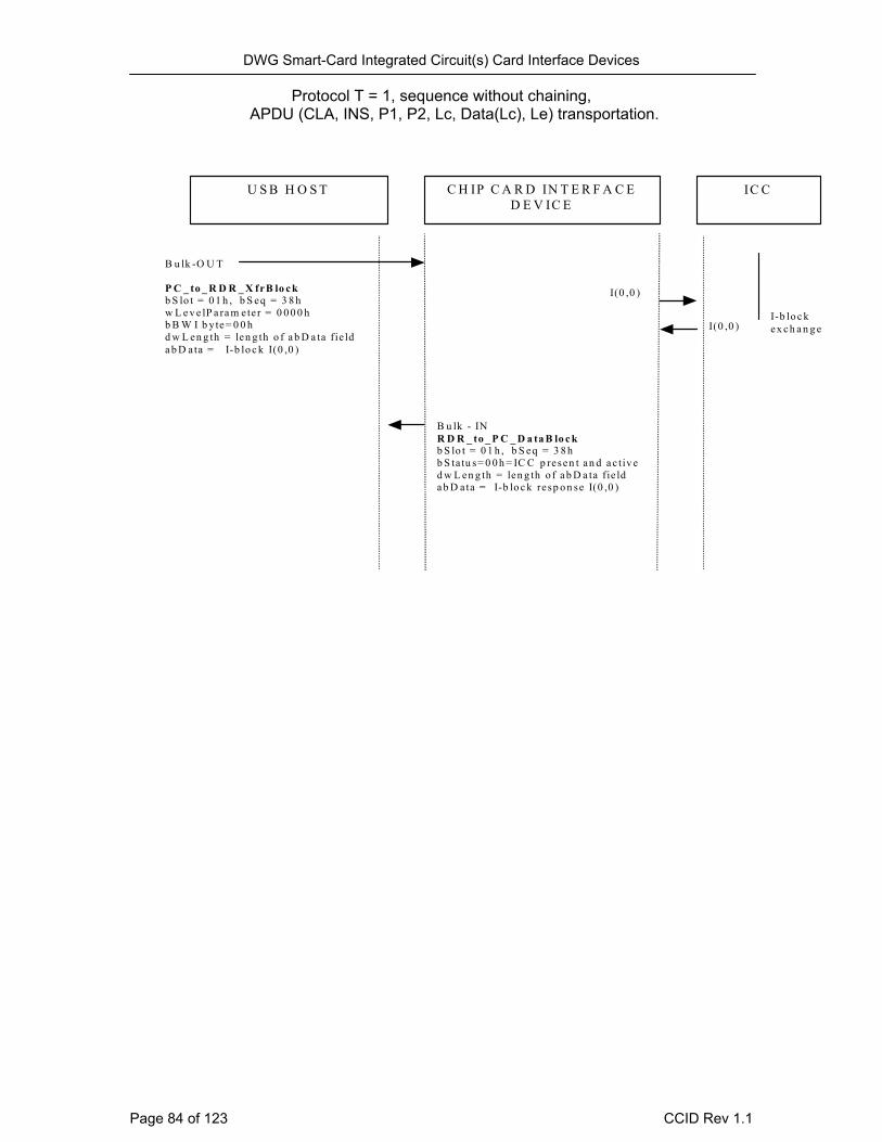
DWG Smart-Card Integrated Circuit(s) Card Interface Devices
Protocol T = 1, sequence without chaining, APDU (CLA, INS, P1, P2, Lc, Data(Lc), Le) transportation.
U S B H O S T C H IP C A R D IN T E R F A C E D E V IC E
I(0 ,0 )
I(0 ,0 )
B u lk - IN R D R _ to _ P C _ D a ta B lo c k b S lo t = 0 1 h , b S eq = 3 8 h b S ta tu s= 0 0 h = IC C p resen t an d a c t iv e d w L en g th = len g th o f a b D a ta fie ld a b D ata = I-b lo c k resp o n se I(0 ,0 )
IC C
B u lk -O U T P C _ to _ R D R _ X frB lo c k b S lo t = 0 1 h , b S eq = 3 8 h w L e v e lP a ra m ete r = 0 0 0 0 h b B W I b y te= 0 0 h d w L en g th = len g th o f a b D a ta f ie ld a b D ata = I-b lo c k I(0 ,0 )
I-b lo c k ex c h a n g e
Page 84 of 123 CCID Rev 1.1

DWG Smart-Card Integrated Circuit(s) Card Interface Devices
Protocol T = 1, sequence with chaining.
U S B H O S T C H IP C A R D IN T E R F A C ED E V IC E
R (1 )I(0 ,0 )
B u lk - INR D R _ to _ P C _ D a ta B lo c kb S lo t = 0 1 h , b S eq = 3 9 hb S ta tu s= 0 0 h = IC C p resen t an d a c t iv ed w L en g th = len g th o f a b D a ta fie lda b D ata = R -b lo c k R (1 )
IC C
B u lk -O U T
P C _ to _ R D R _ X frB lo c kb S lo t = 0 1 h , b S eq = 3 9 hw L e v e lP a ra m ete r = 0 0 0 0 hb B W I b y te= 0 0 hd w L en g th = len g th o f a b D a ta f ie lda b D ata = I-b lo c k I(0 ,1 )
B u lk -O U T
P C _ to _ R D R _ X frB lo c kb S lo t = 0 1 h , b S eq = 3 A hw L e v e lP a ra m ete r = 0 0 0 0 hb B W I b y te= 0 0 hd w L en g th = len g th o f a b D a ta f ie lda b D ata = I-b lo c k I(1 ,0 )
B u lk -O U T
P C _ to _ R D R _ X frB lo c kb S lo t = 0 1 h , b S eq = 3 B hw L e v e lP a ra m ete r = 0 0 0 0 hb B W I b y te= 0 0 hd w L en g th = len g th o f a b D a ta f ie lda b D ata = R -b lo c k R (1 )
B u lk - INR D R _ to _ P C _ D a ta B lo c kb S lo t = 0 1 h , b S eq = 3 A hb S ta tu s= 0 0 h = IC C p resen t an d a c t iv ed w L en g th = len g th o f a b D a ta fie lda b D ata = I-b lo c k resp o n se I(0 ,1 )
B u lk - INR D R _ to _ P C _ D a ta B lo c kb S lo t = 0 1 h , b S eq = 3 B hb S ta tu s= 0 0 h = IC C p resen t an d a c t iv ed w L en g th = len g th o f a b D a ta fie lda b D ata = I-b lo c k resp o n se I(1 ,0 )
I(1 ,0 )
R (1 )
I(0 ,1 )
I(1 ,0 )
CCID Rev 1.1 Page 85 of 123
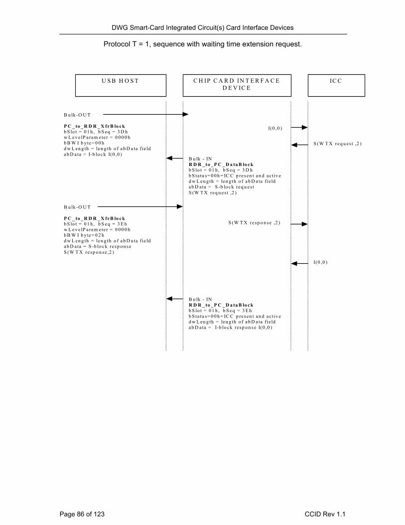
DWG Smart-Card Integrated Circuit(s) Card Interface Devices
Protocol T = 1, sequence with waiting time extension request.
U S B H O S T C H IP C A R D IN T E R F A C ED E V IC E
S (W T X req u es t ,2 )
I(0 ,0 )
B u lk - INR D R _ to _ P C _ D a ta B lo c kb S lo t = 0 1 h , b S eq = 3 D hb S ta tu s= 0 0 h = IC C p resen t an d a c t iv ed w L en g th = len g th o f a b D a ta fie lda b D ata = S -b lo c k req u es tS (W T X req u es t ,2 )
IC C
B u lk -O U T
P C _ to _ R D R _ X frB lo c kb S lo t = 0 1 h , b S eq = 3 D hw L e v e lP a ra m ete r = 0 0 0 0 hb B W I b y te= 0 0 hd w L en g th = len g th o f a b D a ta f ie lda b D ata = I-b lo c k I(0 ,0 )
B u lk - INR D R _ to _ P C _ D a ta B lo c kb S lo t = 0 1 h , b S eq = 3 E hb S ta tu s= 0 0 h = IC C p resen t an d a c t iv ed w L en g th = len g th o f a b D a ta fie lda b D ata = I-b lo c k resp o n se I(0 ,0 )
B u lk -O U T
P C _ to _ R D R _ X frB lo c kb S lo t = 0 1 h , b S eq = 3 E hw L e v e lP a ra m ete r = 0 0 0 0 hb B W I b y te= 0 2 hd w L en g th = len g th o f a b D a ta f ie lda b D ata = S -b lo c k resp o n seS (W T X resp o n se ,2 )
I(0 ,0 )
S (W T X resp o n se ,2 )
Page 86 of 123 CCID Rev 1.1
DWG Smart-Card Integrated Circuit(s) Card Interface Devices
8 Examples of PIN Management 8.1 PIN Verification Examples of format coding for PIN verification:
Format
Example Type Pad PIN Bit Justification Message
BCD ASCII Binary Length Shift Left Right
1 * *
2 * * * 1
3 * * * *
4 * * *
5 * * default
8.1.1 PIN uses a binary format conversion • PIN entered is 12345678 (min and max sizes are 8 digits) • Left justification • No messages • The CCID sends to the ICC the command
CLA INS P1 P2 Lc 01 02 03 04 05 06 07 08
bTimeOut 00 Default time out
bmFormatString
0 0000 0 00 b System unit = bit
PIN position in the frame = 0
PIN justification left
Binary format
bmPINBlockString 0000 1000 b No PIN length management
Length PIN = 8
bmPINLengthFormat 00h No PIN length management
wPINMaxExtraDigit 0808h Min=max = 8 digits
bEntryValidationCondition 01h Max size reach
bNumberMessage 00h No message
wLangId 0409h Language is English
abPINApdu CLA INS P1 P2 08 0000000000000000
APDU Command
Preliminary data: 00h 00h 00h 00h 00h 00h 00h 00h is part of abPINApdu
CCID Rev 1.1 Page 87 of 123

DWG Smart-Card Integrated Circuit(s) Card Interface Devices 8.1.1.1 Initial data mapping by the device Data 1 = 00h Data 2 = 00h Data 3 = 00h
0 0 0 0 0 0 0 0 0 0 0 0 0 0 0 0 0 0 0 0 0 0 0 0
Data 4 = 00h Data 5 = 00h Data 6 = 00h
0 0 0 0 0 0 0 0 0 0 0 0 0 0 0 0 0 0 0 0 0 0 0 0
Data 7 = 00h Data 8 = 00h
0 0 0 0 0 0 0 0 0 0 0 0 0 0 0 0
8.1.1.2 After key entry + Binary conversion + left justification Data 1 = 01h Data 2 = 02h Data 3 = 03h
0 0 0 0 0 0 0 1 0 0 0 0 0 0 1 0 0 0 0 0 0 0 1 1
Data 4 = 04h Data 5 = 05 Data 6 = 06h
0 0 0 0 0 1 0 0 0 0 0 0 0 1 0 1 0 0 0 0 0 1 1 0
Data 7 = 07h Data 8 = 08h
0 0 0 0 0 1 1 1 0 0 0 0 1 0 0 0
Page 88 of 123 CCID Rev 1.1

DWG Smart-Card Integrated Circuit(s) Card Interface Devices 8.1.2 PIN uses a shift rotation format conversion. • PIN entered is 4330 (min and max sizes are 4 digits) • Left justification • 1 message “ENTER PIN” • The CCID sends to the ICC the command
CLA INS P1 P2 Lc 10 CC 3F FF
bTimeOut 00h Default time out
bmFormatString 0 0010 0 01 b System unit = bit
PIN position in the frame = 2 bit
PIN justification left
BCD format
bmPINBlockString 0000 0100 b No PIN length management
Length PIN = 4 bytes
bmPINLengthFormat 00h No PIN length management
wPINMaxExtraDigit 0404h Min=max = 4 digits
bEntryValidationCondition 01h Max size reach
bNumberMessage 01h One message
wLangId 040Ch Language is French
bMsgIndex 0h Message index for ENTER PIN
abPINApdu Cla INS P1 P2 04 00003FFF APDU command
Preliminary data: 00h 00h 3Fh FFh is part of abPINApdu
CCID Rev 1.1 Page 89 of 123

DWG Smart-Card Integrated Circuit(s) Card Interface Devices 8.1.2.1 Initial data mapping Data 1 = 00h Data 2 = 00h Data 3 = 3Fh
0 0 0 0 0 0 0 0 0 0 0 0 0 0 0 0 0 0 1 1 1 1 1 1
Sys. Bit Secret code byte 1 (2digits). Secret code byte 2 (2 digits) Automatic-
Data 4 = FFh
1 1 1 1 1 1 1 1
-Padding Operation 8.1.2.2 After key entry + left justification Data 1 = 10h Data 2 = CCh Data 3 = 3Fh
0 0 0 1 0 0 0 0 1 1 0 0 1 1 0 0 0 0 1 1 1 1 1 1 PIN digit values: 4 and 3 3 and 0
Data 4 = FFh
1 1 1 1 1 1 1 1
Page 90 of 123 CCID Rev 1.1
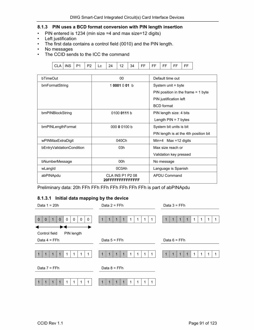
DWG Smart-Card Integrated Circuit(s) Card Interface Devices 8.1.3 PIN uses a BCD format conversion with PIN length insertion • PIN entered is 1234 (min size =4 and max size=12 digits) • Left justification • The first data contains a control field (0010) and the PIN length. • No messages • The CCID sends to the ICC the command
CLA INS P1 P2 Lc 24 12 34 FF FF FF FF FF
bTimeOut 00 Default time out
bmFormatString 1 0001 0 01 b System unit = byte
PIN position in the frame = 1 byte
PIN justification left
BCD format
bmPINBlockString 0100 0111 b PIN length size: 4 bits
Length PIN = 7 bytes
bmPINLengthFormat 000 0 0100 b System bit units is bit
PIN length is at the 4th position bit
wPINMaxExtraDigit 040Ch Min=4 Max =12 digits
bEntryValidationCondition 03h Max size reach or
Validation key pressed
bNumberMessage 00h No message
wLangId 0C0Ah Language is Spanish
abPINApdu CLA INS P1 P2 08 20FFFFFFFFFFFFFF
APDU Command
Preliminary data: 20h FFh FFh FFh FFh FFh FFh FFh is part of abPINApdu 8.1.3.1 Initial data mapping by the device Data 1 = 20h Data 2 = FFh Data 3 = FFh
0 0 1 0 0 0 0 0 1 1 1 1 1 1 1 1 1 1 1 1 1 1 1 1
Control field PIN length
Data 4 = FFh Data 5 = FFh Data 6 = FFh
1 1 1 1 1 1 1 1 1 1 1 1 1 1 1 1 1 1 1 1 1 1 1 1
Data 7 = FFh Data 8 = FFh
1 1 1 1 1 1 1 1 1 1 1 1 1 1 1 1
CCID Rev 1.1 Page 91 of 123

DWG Smart-Card Integrated Circuit(s) Card Interface Devices 8.1.3.2 After key entry + left justification Data 1 = 24h Data 2 = 12h Data 3 = 34h
0 0 1 0 0 1 0 0 0 0 0 1 0 0 1 0 0 0 1 1 0 1 0 0
PIN length
Data 4 = FFh Data 5 = FFh Data 6 = FFh
1 1 1 1 1 1 1 1 1 1 1 1 1 1 1 1 1 1 1 1 1 1 1 1
Data 7 = FFh Data 8 = FFh
1 1 1 1 1 1 1 1 1 1 1 1 1 1 1 1
Page 92 of 123 CCID Rev 1.1
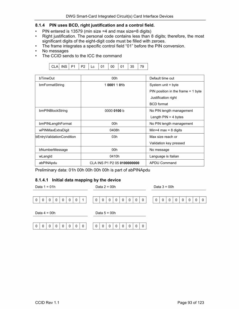
DWG Smart-Card Integrated Circuit(s) Card Interface Devices 8.1.4 PIN uses BCD, right justification and a control field. • PIN entered is 13579 (min size =4 and max size=8 digits) • Right justification. The personal code contains less than 8 digits; therefore, the most
significant digits of the eight-digit code must be filled with zeroes. • The frame integrates a specific control field “01” before the PIN conversion. • No messages • The CCID sends to the ICC the command
CLA INS P1 P2 Lc 01 00 01 35 79
bTimeOut 00h Default time out
bmFormatString 1 0001 1 01b System unit = byte
PIN position in the frame = 1 byte
Justification right
BCD format
bmPINBlockString 0000 0100 b No PIN length management
Length PIN = 4 bytes
bmPINLengthFormat 00h No PIN length management
wPINMaxExtraDigit 0408h Min=4 max = 8 digits
bEntryValidationCondition 03h Max size reach or
Validation key pressed
bNumberMessage 00h No message
wLangId 0410h Language is Italian
abPINApdu CLA INS P1 P2 05 0100000000 APDU Command
Preliminary data: 01h 00h 00h 00h 00h is part of abPINApdu 8.1.4.1 Initial data mapping by the device Data 1 = 01h Data 2 = 00h Data 3 = 00h
0 0 0 0 0 0 0 1 0 0 0 0 0 0 0 0 0 0 0 0 0 0 0 0
Data 4 = 00h Data 5 = 00h
0 0 0 0 0 0 0 0 0 0 0 0 0 0 0 0
CCID Rev 1.1 Page 93 of 123

DWG Smart-Card Integrated Circuit(s) Card Interface Devices 8.1.4.2 After key entry + right justification Data 1 = 01h Data 2 = 00h Data 3 = 01h
0 0 0 0 0 0 0 1 0 0 0 0 0 0 0 0 0 0 0 0 0 0 0 1
Data 4 = 35h Data 5 = 79h
0 0 1 1 0 1 0 1 0 1 1 1 1 0 0 1
Page 94 of 123 CCID Rev 1.1
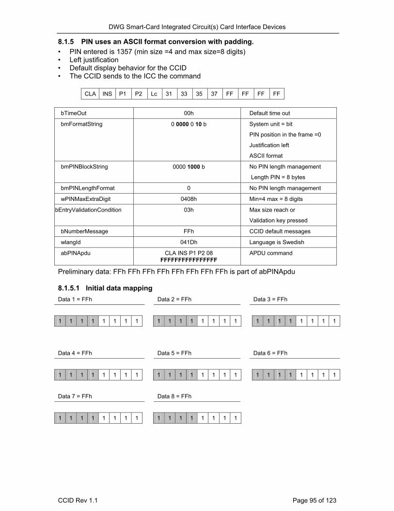
DWG Smart-Card Integrated Circuit(s) Card Interface Devices 8.1.5 PIN uses an ASCII format conversion with padding. • PIN entered is 1357 (min size =4 and max size=8 digits) • Left justification • Default display behavior for the CCID • The CCID sends to the ICC the command
CLA INS P1 P2 Lc 31 33 35 37 FF FF FF FF
bTimeOut 00h Default time out
bmFormatString 0 0000 0 10 b System unit = bit
PIN position in the frame =0
Justification left
ASCII format
bmPINBlockString 0000 1000 b No PIN length management
Length PIN = 8 bytes
bmPINLengthFormat 0 No PIN length management
wPINMaxExtraDigit 0408h Min=4 max = 8 digits
bEntryValidationCondition 03h Max size reach or
Validation key pressed
bNumberMessage FFh CCID default messages
wlangId 041Dh Language is Swedish
abPINApdu CLA INS P1 P2 08 FFFFFFFFFFFFFFFF
APDU command
Preliminary data: FFh FFh FFh FFh FFh FFh FFh FFh is part of abPINApdu 8.1.5.1 Initial data mapping Data 1 = FFh Data 2 = FFh Data 3 = FFh
1 1 1 1 1 1 1 1 1 1 1 1 1 1 1 1 1 1 1 1 1 1 1 1
Data 4 = FFh Data 5 = FFh Data 6 = FFh
1 1 1 1 1 1 1 1 1 1 1 1 1 1 1 1 1 1 1 1 1 1 1 1
Data 7 = FFh Data 8 = FFh
1 1 1 1 1 1 1 1 1 1 1 1 1 1 1 1
CCID Rev 1.1 Page 95 of 123

DWG Smart-Card Integrated Circuit(s) Card Interface Devices 8.1.5.2 PIN + left justification Data 1 = 31h Data 2 = 33h Data 3 = 35h
0 0 1 1 0 0 0 1 0 0 1 1 0 0 1 1 0 0 1 1 0 1 0 1
Data 4 = 37h Data 5 = FFh Data 6 = FFh
0 0 1 1 1 1 1 1 1 1 1 1 1 1 1 1 1 1 1 1 1 1 1 1
Padding with F character
Data 7 = FFh Data 8 = FFh
1 1 1 1 1 1 1 1 1 1 1 1 1 1 1 1
Page 96 of 123 CCID Rev 1.1
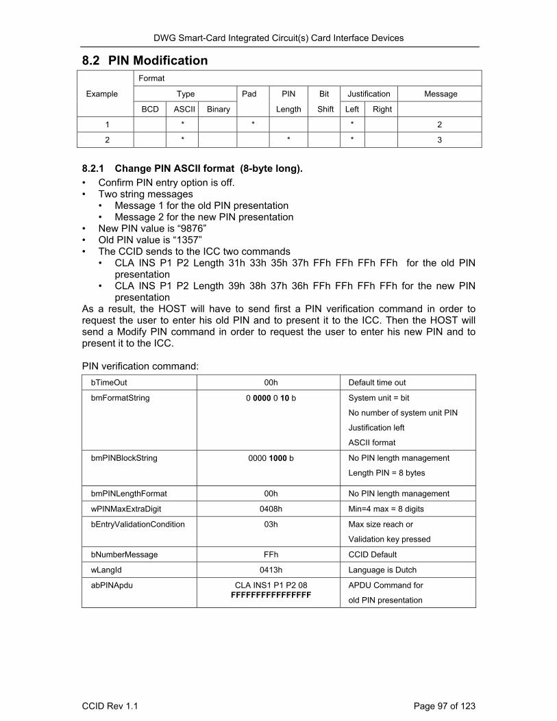
DWG Smart-Card Integrated Circuit(s) Card Interface Devices
8.2 PIN Modification Format
Example Type Pad PIN Bit Justification Message
BCD ASCII Binary Length Shift Left Right
1 * * * 2
2 * * * 3
8.2.1 Change PIN ASCII format (8-byte long). • Confirm PIN entry option is off. • Two string messages
• Message 1 for the old PIN presentation • Message 2 for the new PIN presentation
• New PIN value is “9876” • Old PIN value is “1357” • The CCID sends to the ICC two commands
• CLA INS P1 P2 Length 31h 33h 35h 37h FFh FFh FFh FFh for the old PIN presentation
• CLA INS P1 P2 Length 39h 38h 37h 36h FFh FFh FFh FFh for the new PIN presentation
As a result, the HOST will have to send first a PIN verification command in order to request the user to enter his old PIN and to present it to the ICC. Then the HOST will send a Modify PIN command in order to request the user to enter his new PIN and to present it to the ICC. PIN verification command:
bTimeOut 00h Default time out
bmFormatString 0 0000 0 10 b System unit = bit
No number of system unit PIN
Justification left
ASCII format
bmPINBlockString 0000 1000 b No PIN length management
Length PIN = 8 bytes
bmPINLengthFormat 00h No PIN length management
wPINMaxExtraDigit 0408h Min=4 max = 8 digits
bEntryValidationCondition 03h Max size reach or
Validation key pressed
bNumberMessage FFh CCID Default
wLangId 0413h Language is Dutch
abPINApdu CLA INS1 P1 P2 08 FFFFFFFFFFFFFFFF
APDU Command for
old PIN presentation
CCID Rev 1.1 Page 97 of 123
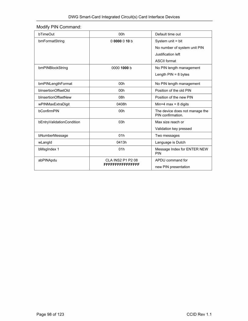
DWG Smart-Card Integrated Circuit(s) Card Interface Devices Modify PIN Command: bTimeOut 00h Default time out
bmFormatString 0 0000 0 10 b System unit = bit
No number of system unit PIN
Justification left
ASCII format
bmPINBlockString 0000 1000 b No PIN length management
Length PIN = 8 bytes
bmPINLengthFormat 00h No PIN length management
bInsertionOffsetOld 00h Position of the old PIN
bInsertionOffsetNew 08h Position of the new PIN
wPINMaxExtraDigit 0408h Min=4 max = 8 digits
bConfirmPIN 00h The device does not manage the PIN confirmation.
bEntryValidationCondition 03h Max size reach or
Validation key pressed
bNumberMessage 01h Two messages
wLangId 0413h Language is Dutch
bMsgIndex 1 01h Message Index for ENTER NEW PIN
abPINApdu CLA INS2 P1 P2 08 FFFFFFFFFFFFFFFF
APDU command for
new PIN presentation
Page 98 of 123 CCID Rev 1.1
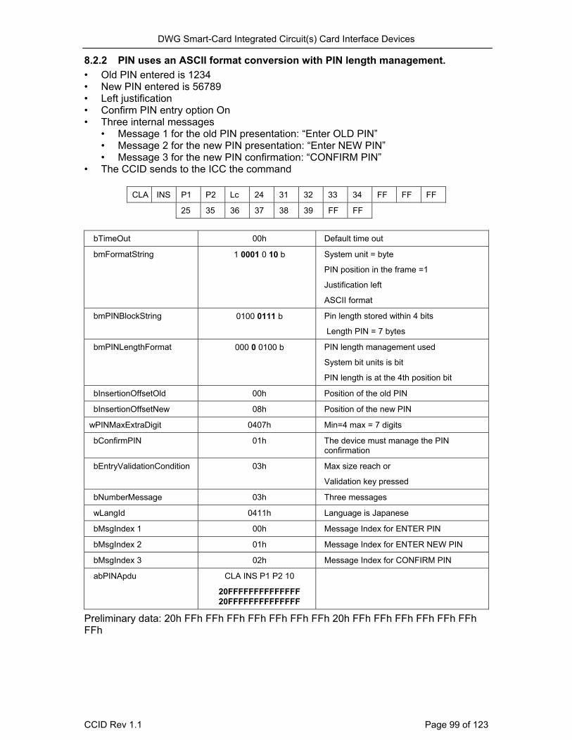
DWG Smart-Card Integrated Circuit(s) Card Interface Devices 8.2.2 PIN uses an ASCII format conversion with PIN length management. • Old PIN entered is 1234 • New PIN entered is 56789 • Left justification • Confirm PIN entry option On • Three internal messages
• Message 1 for the old PIN presentation: “Enter OLD PIN” • Message 2 for the new PIN presentation: “Enter NEW PIN” • Message 3 for the new PIN confirmation: “CONFIRM PIN”
• The CCID sends to the ICC the command
CLA INS P1 P2 Lc 24 31 32 33 34 FF FF FF
25 35 36 37 38 39 FF FF
bTimeOut 00h Default time out
bmFormatString 1 0001 0 10 b System unit = byte
PIN position in the frame =1
Justification left
ASCII format
bmPINBlockString 0100 0111 b Pin length stored within 4 bits
Length PIN = 7 bytes
bmPINLengthFormat 000 0 0100 b PIN length management used
System bit units is bit
PIN length is at the 4th position bit
bInsertionOffsetOld 00h Position of the old PIN
bInsertionOffsetNew 08h Position of the new PIN
wPINMaxExtraDigit 0407h Min=4 max = 7 digits
bConfirmPIN 01h The device must manage the PIN confirmation
bEntryValidationCondition 03h Max size reach or
Validation key pressed
bNumberMessage 03h Three messages
wLangId 0411h Language is Japanese
bMsgIndex 1 00h Message Index for ENTER PIN
bMsgIndex 2 01h Message Index for ENTER NEW PIN
bMsgIndex 3 02h Message Index for CONFIRM PIN
abPINApdu CLA INS P1 P2 10
20FFFFFFFFFFFFFF 20FFFFFFFFFFFFFF
Preliminary data: 20h FFh FFh FFh FFh FFh FFh FFh 20h FFh FFh FFh FFh FFh FFh FFh
CCID Rev 1.1 Page 99 of 123
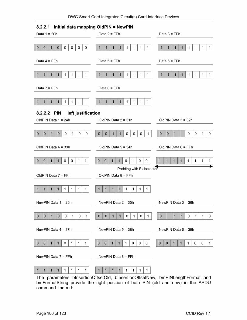
DWG Smart-Card Integrated Circuit(s) Card Interface Devices 8.2.2.1 Initial data mapping OldPIN = NewPIN Data 1 = 20h Data 2 = FFh Data 3 = FFh
0 0 1 0 0 0 0 0 1 1 1 1 1 1 1 1 1 1 1 1 1 1 1 1
Data 4 = FFh Data 5 = FFh Data 6 = FFh
1 1 1 1 1 1 1 1 1 1 1 1 1 1 1 1 1 1 1 1 1 1 1 1
Data 7 = FFh Data 8 = FFh
1 1 1 1 1 1 1 1 1 1 1 1 1 1 1 1
8.2.2.2 PIN + left justification OldPIN Data 1 = 24h OldPIN Data 2 = 31h OldPIN Data 3 = 32h
0 0 1 0 0 1 0 0 0 0 1 1 0 0 0 1 0 0 1 0 0 1 0 1
OldPIN Data 4 = 33h OldPIN Data 5 = 34h OldPIN Data 6 = FFh
0 0 1 1 0 0 1 1 0 0 1 1 0 1 0 0 1 1 1 1 1 1 1 1
Padding with F character
OldPIN Data 7 = FFh OldPIN Data 8 = FFh
1 1 1 1 1 1 1 1 1 1 1 1 1 1 1 1
NewPIN Data 1 = 25h NewPIN Data 2 = 35h NewPIN Data 3 = 36h
0 0 1 0 0 1 0 1 0 0 1 1 0 1 0 1 0 1 1 0 1 1 0 0
NewPIN Data 4 = 37h NewPIN Data 5 = 38h NewPIN Data 6 = 39h
0 0 1 1 0 1 1 1 0 0 1 1 1 0 0 0 0 0 1 1 0 0 1 1
NewPIN Data 7 = FFh NewPIN Data 8 = FFh
1 1 1 1 1 1 1 1 1 1 1 1 1 1 1 1
The parameters bInsertionOffsetOld, bInsertionOffsetNew, bmPINLengthFormat and bmFormatString provide the right position of both PIN (old and new) in the APDU command. Indeed:
Page 100 of 123 CCID Rev 1.1
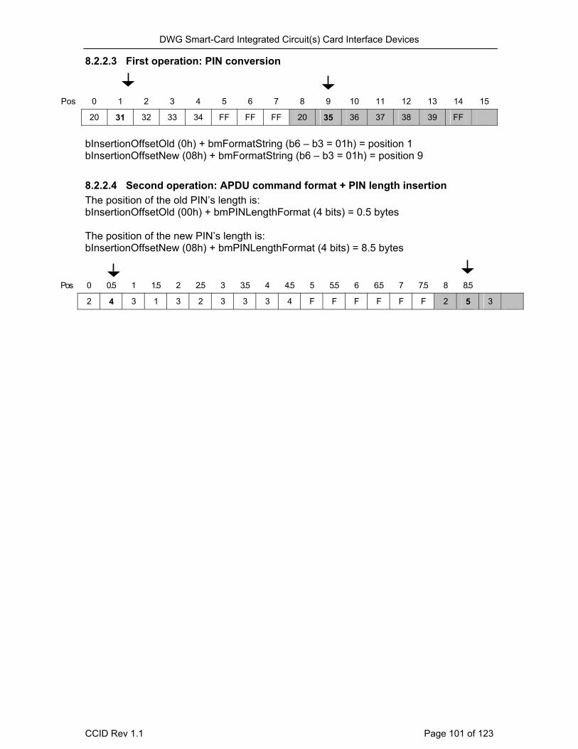
DWG Smart-Card Integrated Circuit(s) Card Interface Devices 8.2.2.3 First operation: PIN conversion
Pos 0 1 2 3 4 5 6 7 8 9 10 11 12 13 14 15
20 31 32 33 34 FF FF FF 20 35 36 37 38 39 FF FF
bInsertionOffsetOld (0h) + bmFormatString (b6 – b3 = 01h) = position 1 bInsertionOffsetNew (08h) + bmFormatString (b6 – b3 = 01h) = position 9
8.2.2.4 Second operation: APDU command format + PIN length insertion The position of the old PIN’s length is: bInsertionOffsetOld (00h) + bmPINLengthFormat (4 bits) = 0.5 bytes The position of the new PIN’s length is: bInsertionOffsetNew (08h) + bmPINLengthFormat (4 bits) = 8.5 bytes
Pos 0 0.5 1 1.5 2 2.5 3 3.5 4 4.5 5 5.5 6 6.5 7 7.5 8 8.5
3 2 4 3 1 2 3 3 3 4 F F F F F F 2 5 5.. 3
CCID Rev 1.1 Page 101 of 123

DWG Smart-Card Integrated Circuit(s) Card Interface Devices 8.2.3 Character Level, Protocol T = 0, sequence for PIN verification
U S B H O S T C H IP C A R D IN T E R F A C ED E V IC E
B u lk -O U T
P C _ to _ R D R _ S ec u reb S lo t = 0 1 h , b S eq = 0 C hw L e v e lP a ra m ete r = 0 0 0 1 hb B W I b y te= 0 0 hd w L en g th = len g th o f d a ta s tru c tu rea b D ata = (C L A ,IN S ,P 1 ,P 2 ,P 3 ) =IC C c o m m an db P IN O p era t io n = 0 0 h (v e rify P IN )O th er f ie ld s : P IN d esc rip tio n 6 0
C L A ,IN S ,P 1 ,P 2 ,P 3
B u lk - INR D R _ to _ P C _ D a ta B lo c kb S lo t = 0 1 h , b S eq = 0 C hb S ta tu s= 0 0 h = IC C p resen t an d a c t iv ed w L en g th = 0 0 0 0 0 0 0 1 ha b D ata = (6 0 h ) = p ro c ed u re b y te
IC C
D a ta (F o rm a tted P IN )
9 0 ,0 0
B u lk -O U T
P C _ to _ R D R _ S ec u reb S lo t = 0 1 h , b S eq = 0 D hw L e v e lP a ra m ete r = 0 0 0 1 hb B W I b y te= 0 0 hd w L en g th = 0 0 0 0 0 0 0 0 ha b D ata is a b sen t b P IN O p era tio n = 0 3 h (w a it IC Cresp o n se)O th er f ie ld s : n o th in g
B u lk -O U T
P C _ to _ R D R _ S ec u reb S lo t = 0 1 h , b S eq = 0 E hw L e v e lP a ra m ete r = 0 0 0 2 hb B W I b y te= 0 0 hd w L en g th = 0 0 0 0 0 0 0 0 ha b D ata is a b sen tb P IN O p era t io n = 0 2 h (tra n sfe r P IN )O th er f ie ld s : n o th in g
B u lk - INR D R _ to _ P C _ D a ta B lo c kb S lo t = 0 1 h , b S eq = 0 D hb S ta tu s= 0 0 h = IC C p resen t an d a c t iv ed w L en g th = 0 0 0 0 0 0 0 1 ha b D ata = (IN S ) = p ro c ed u re b y te
B u lk - INR D R _ to _ P C _ D a ta B lo c kb S lo t = 0 1 h , b S eq = 0 E hb S ta tu s= 0 0 h = IC C p resen t an d a c t iv ed w L en g th = 0 0 0 0 0 0 0 2 ha b D ata = (9 0 h ,0 0 h ) = IC C resp o n se
IN S
C C ID d isp la y s m e s sa g e , e n a b le s k e y p a d , a n d u se r e n te rs P IN .
Notes: In case of procedure byte equal to 60h, the host asks for 1 byte which means, for the CCID, that another procedure byte is waiting (thus the code is not sent to the ICC). In case of procedure byte equal to INS, the host asks for 2 bytes which means, for the CCID, that it can send the code to the ICC and wait for 2 bytes from the ICC (SW1, SW2).
Page 102 of 123 CCID Rev 1.1
DWG Smart-Card Integrated Circuit(s) Card Interface Devices
9 Sample diagrams based on dwFeatures The sequences are not exhaustive of all the possible cases. They are only meant as examples of several of the possible sequences the CCID must be able to handle.
9.1 Definition of dwFeatures fields FEATURE 1 (0002067Eh) : - Short APDU exchange level. - Automatic IFSD exchange. - NAD value other than 00h accepted. - Automatic PPS made by the CCID (proprietary algorithm). - Automatic baud rate change according to parameters. - Automatic ICC clock frequency change according to parameters. - Automatic voltage selection. - Automatic ICC activation on insertion. - Automatic parameters configuration based on ATR data. FEATURE 2 (000206B2h) : - Short APDU exchange level. - Automatic IFSD exchange. - NAD value other than 00h accepted. - Automatic PPS according to current parameters. - Automatic baud rate change according to parameters. - Automatic ICC clock frequency change according to parameters. - Automatic parameters configuration based on ATR data. FEATURE 3 (000104B2h) : - TPDU level exchange. - Automatic IFSD exchange. - Automatic PPS according to current parameters. - Automatic baud rate change according to parameters. - Automatic ICC clock frequency change according to parameters. - Automatic parameters configuration based on ATR data. FEATURE 4 (00010230h) : - TPDU level exchange - NAD value other than 00h accepted. - Automatic baud rate change according to parameters - Automatic ICC clock frequency change according to parameters FEATURE 5 (00000030h) : - Character level - Automatic baud rate change according to parameters - Automatic ICC clock frequency change according to parameters FEATURE 6 (00000000h) : - No special characteristics (character level exchange, no automatism)
CCID Rev 1.1 Page 103 of 123
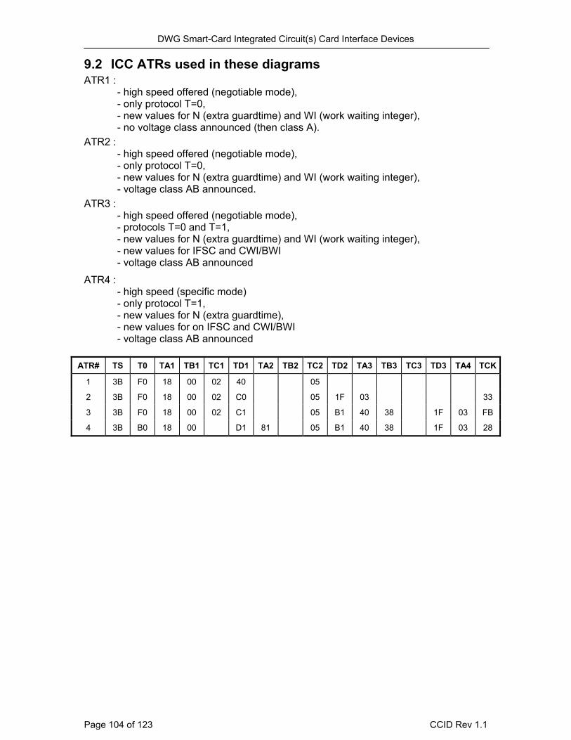
DWG Smart-Card Integrated Circuit(s) Card Interface Devices 9.2 ICC ATRs used in these diagrams ATR1 : - high speed offered (negotiable mode), - only protocol T=0, - new values for N (extra guardtime) and WI (work waiting integer), - no voltage class announced (then class A). ATR2 : - high speed offered (negotiable mode), - only protocol T=0, - new values for N (extra guardtime) and WI (work waiting integer), - voltage class AB announced. ATR3 : - high speed offered (negotiable mode), - protocols T=0 and T=1, - new values for N (extra guardtime) and WI (work waiting integer), - new values for IFSC and CWI/BWI - voltage class AB announced
TB1
ATR4 : - high speed (specific mode) - only protocol T=1, - new values for N (extra guardtime), - new values for on IFSC and CWI/BWI - voltage class AB announced
ATR# TS T0 TA1 TC1 TD1 TA2 TB2 TC2 TD2 TA3 TB3 TC3 TD3 TA4 TCK
1 3B F0 18 00 02 40 05
2 3B F0 18 05 00 02 C0 1F 03 33
3 3B F0 18 00 02 C1 05 B1 40 38 1F 03 FB
3B B0 18 00 D1 81 05 B1 40 38 1F 28 4 03
Page 104 of 123 CCID Rev 1.1
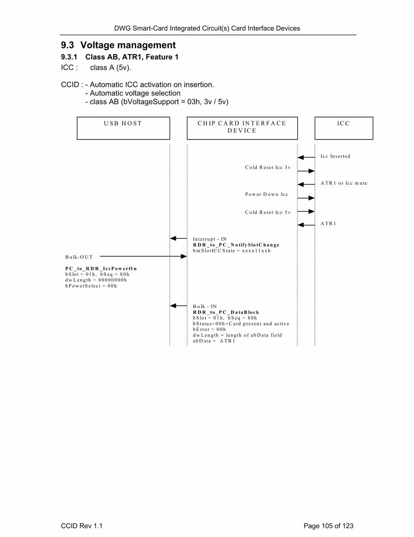
DWG Smart-Card Integrated Circuit(s) Card Interface Devices
9.3 Voltage management 9.3.1 Class AB, ATR1, Feature 1 ICC : class A (5v). CCID : - Automatic ICC activation on insertion.
- Automatic voltage selection - class AB (bVoltageSupport = 03h, 3v / 5v)
U S B H O S T C H IP C A R D IN T E R F A C ED E V IC E
A T R 1 o r Ic c m u te
C o ld R ese t Ic c 3 v
B u lk - INR D R _ to _ P C _ D a ta B lo c kb S lo t = 0 1 h , b S eq = 8 0 hb S ta tu s= 0 0 h = C a rd p resen t an d ac tiv eb E rro r = 0 0 hd w L en g th = len g th o f a b D a ta fie lda b D ata = A T R 1
IC C
B u lk -O U T
P C _ to _ R D R _ Ic c P o w er O nb S lo t = 0 1 h , b S eq = 8 0 hd w L en g th = 0 0 0 0 0 0 0 0 hb P o w e rS e lec t = 0 0 h
A T R 1
Ic c In se rted
P o w er D o w n Ic c
In te rru p t - INR D R _ to _ P C _ N o tify S lo tC h a n g eb m S lo tIC C S ta te = x x x x 1 1 x x b
C o ld R ese t Ic c 5 v
CCID Rev 1.1 Page 105 of 123
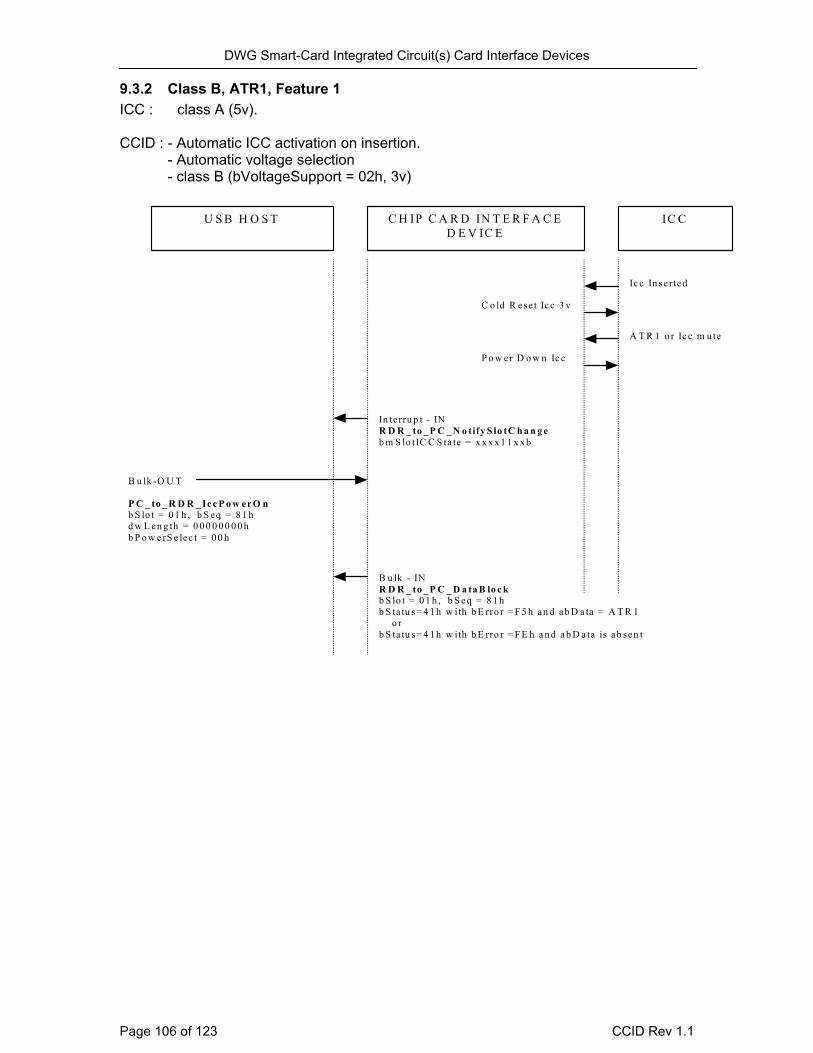
DWG Smart-Card Integrated Circuit(s) Card Interface Devices 9.3.2 Class B, ATR1, Feature 1 ICC : class A (5v). CCID : - Automatic ICC activation on insertion. - Automatic voltage selection - class B (bVoltageSupport = 02h, 3v)
U S B H O S T C H IP C A R D IN T E R F A C ED E V IC E
A T R 1 o r Ic c m u te
C o ld R ese t Ic c 3 v
B u lk - INR D R _ to _ P C _ D a ta B lo c kb S lo t = 0 1 h , b S eq = 8 1 hb S ta tu s= 4 1 h w ith b E rro r = F 5 h an d ab D a ta = A T R 1 o rb S ta tu s= 4 1 h w ith b E rro r = F E h a n d a b D a ta is ab sen t
IC C
B u lk -O U T
P C _ to _ R D R _ Ic c P o w er O nb S lo t = 0 1 h , b S eq = 8 1 hd w L en g th = 0 0 0 0 0 0 0 0 hb P o w e rS e lec t = 0 0 h
Ic c In se rted
P o w er D o w n Ic c
In te rru p t - INR D R _ to _ P C _ N o tify S lo tC h a n g eb m S lo tIC C S ta te = x x x x 1 1 x x b
Page 106 of 123 CCID Rev 1.1

DWG Smart-Card Integrated Circuit(s) Card Interface Devices 9.3.3 Class AB, ATR1, Feature 2, 3, 4, 5 and Feature 5 ICC : class A (5v). CCID : - no automatic feature on insertion or for voltage selection.
- class AB (bVoltageSupport = 03h, 3v / 5v)
U S B H O S T C H IP C A R D IN T E R F A C ED E V IC E
A T R 1 o r Ic c m u teC o ld R ese t Ic c 3 v
B u lk - INR D R _ to _ P C _ D a ta B lo c kb S lo t = 0 1 h , b S eq = 8 2 hb S ta tu s= 0 0 h w ith b E rro r = 0 0 h a n d a b D a ta = A T R 1 o rb S ta tu s= 4 0 h w ith b E rro r = F E h a n d a b D a ta is ab sen t
IC C
B u lk -O U T
P C _ to _ R D R _ Ic c P o w er O nb S lo t = 0 1 h , b S eq = 8 2 hd w L en g th = 0 0 0 0 0 0 0 0 hb P o w e rS e lec t = 0 2 h
Ic c In se rted
P o w er D o w n Ic c
In te rru p t - INR D R _ to _ P C _ N o tify S lo tC h a n g eb m S lo tIC C S ta te = x x x x 1 1 x x b
B u lk -O U T
P C _ to _ R D R _ C a r d P o w er O ffb S lo t = 0 1 h , b S eq = 8 3 h
B u lk -O U T
P C _ to _ R D R _ C a r d P o w er O nb S lo t = 0 1 h , b S eq = 8 4 hd w L en g th = 0 0 0 0 0 0 0 0 hb P o w e rS e lec t = 0 1 h
B u lk - INR D R _ to _ P C _ P C S lo tS ta tu sb S lo t = 0 1 h , b S eq = 8 3 hb S ta tu s= 0 0 h w ith b E rro r = 0 0 h
B u lk - INR D R _ to _ P C _ D a ta B lo c kb S lo t = 0 1 h , b S eq = 8 4 hb S ta tu s= 0 0 h w ith b E rro r = 0 0 ha b D ata = A T R 1
A T R 1
C o ld R ese t Ic c 5 v
CCID Rev 1.1 Page 107 of 123

DWG Smart-Card Integrated Circuit(s) Card Interface Devices 9.3.4 Class AB, ATR2, Feature 2, 3, 4 and Feature 5 ICC : class AB (3v / 5v).
CCID : - no automatic feature on insertion or for voltage selection. - class AB (bVoltageSupport = 03h, 3v / 5v)
U S B H O S T C H IP C A R D IN T E R F A C ED E V IC E
A T R 2C o ld R ese t Ic c 3 v
B u lk - INR D R _ to _ P C _ D a ta B lo c kb S lo t = 0 1 h , b S eq = 8 B hb S ta tu s= 0 0 h w ith b E rro r = 0 0 h a b D a ta = A T R 2
IC C
B u lk -O U T
P C _ to _ R D R _ Ic c P o w er O nb S lo t = 0 1 h , b S eq = 8 B hd w L en g th = 0 0 0 0 0 0 0 0 hb P o w e rS e lec t = 0 2 h
Ic c In se rted
In te rru p t - INR D R _ to _ P C _ N o tify S lo tC h a n g eb m S lo tIC C S ta te = x x x x 1 1 x x b
Page 108 of 123 CCID Rev 1.1
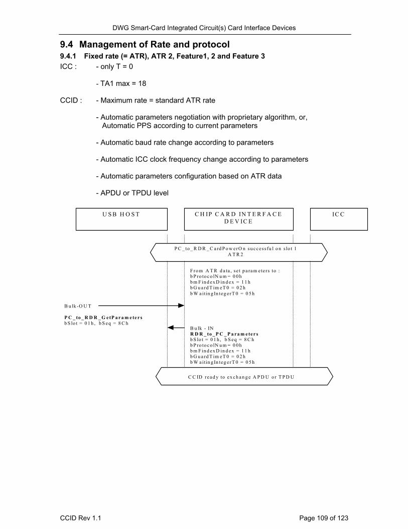
DWG Smart-Card Integrated Circuit(s) Card Interface Devices
9.4 Management of Rate and protocol 9.4.1 Fixed rate (= ATR), ATR 2, Feature1, 2 and Feature 3 ICC : - only T = 0
- Automatic parameters negotiation with proprietary algorithm, or, Automatic PPS according to current parameters
- TA1 max = 18
CCID : - Maximum rate = standard ATR rate
- Automatic baud rate change according to parameters - Automatic ICC clock frequency change according to parameters - Automatic parameters configuration based on ATR data - APDU or TPDU level
U S B H O S T C H IP C A R D IN T E R F A C ED E V IC E
B u lk - INR D R _ to _ P C _ P a ra m e te r sb S lo t = 0 1 h , b S eq = 8 C hb P ro to c o lN u m = 0 0 hb m F in d ex D in d ex = 1 1 hb G u a rd T im eT 0 = 0 2 hb W a itin g In teg erT 0 = 0 5 h
IC C
B u lk -O U T
P C _ to _ R D R _ G e tP a r a m e te r sb S lo t = 0 1 h , b S eq = 8 C h
F ro m A T R d a ta , se t p a ra m ete rs to :b P ro to c o lN u m = 0 0 hb m F in d ex D in d ex = 1 1 hb G u a rd T im eT 0 = 0 2 hb W a itin g In teg erT 0 = 0 5 h
P C _ to _ R D R _ C a rd P o w erO n su c c ess fu l o n s lo t 1A T R 2
C C ID rea d y to ex c h a n g e A P D U o r T P D U
CCID Rev 1.1 Page 109 of 123

DWG Smart-Card Integrated Circuit(s) Card Interface Devices 9.4.2 High speed, ATR 4, Feature 1 or Feature 2 ICC : - T = 0 and T = 1 - Specific mode with TA1 = 18
CCID : - Maximum rate > (Maximum frequency * 12) / 372
- Automatic parameters negotiation with proprietary algorithm, or, Automatic PPS according to current parameters
- Automatic baud rate change according to parameters - Automatic ICC clock frequency change according to parameters - Automatic parameters configuration based on ATR data - APDU level
U S B H O S T C H IP C A R D IN T E R F A C ED E V IC E
B u lk - INR D R _ to _ P C _ P a ra m e te r sb S lo t = 0 1 h , b S eq = 8 D hb P ro to c o lN u m = 0 1 hb m F in d ex D in d ex = 1 8 hb m T C C K S T 1 = 1 0 hb G u a rd T im eT 1 = 0 2 hb W a itin g In teg ers T 1 = 3 8 h
IC C
B u lk -O U T
P C _ to _ R D R _ G e tP a r a m e te r sb S lo t = 0 1 h , b S eq = 8 D h
F ro m A T R d a ta , se t p a ra m ete rs to :b P ro to c o lN u m = 0 1 hb m F in d ex D in d ex = 1 8 hb m T C C K S T 1 = 1 0 hb G u a rd T im eT 1 = 0 2 hb W a itin g In teg ers T 1 = 3 8 h
P C _ to _ R D R _ C a rd P o w erO n su c c ess fu l o n s lo t 1A T R 4
C C ID rea d y to ex c h a n g e A P D U
Page 110 of 123 CCID Rev 1.1

DWG Smart-Card Integrated Circuit(s) Card Interface Devices 9.4.3 Fixed rate (= ATR), ATR 2, Feature 4 or Feature 5
- Automatic baud rate change according to parameters
ICC : - only T = 0 - TA1 max = 18 CCID : - Maximum rate = standard ATR rate
- Automatic ICC clock frequency change according to parameters - TPDU or Character level
U S B H O S T C H IP C A R D IN T E R F A C ED E V IC E
B u lk - INR D R _ to _ P C _ P a ra m e te r sb S lo t = 0 1 h , b S eq = 8 E hb P ro to c o lN u m = 0 0 hb m F in d ex D in d ex = 1 1 hb G u a rd T im eT 0 = 0 2 hb W a itin g In teg erT 0 = 0 5 h
IC C
B u lk -O U T
P C _ to _ R D R _ S e tP a r a m e te r sb S lo t = 0 1 h , b S eq = 8 E hb P ro to c o lN u m = 0 0 h ,b m F in d ex D in d ex = 1 1 h ,b G u a rd T im eT 0 = 0 2 hb W a itin g In teg erT 0 = 0 5 h
P a ra m ete rs se t to d e fa u lt:b P ro to c o lN u m = 0 0 hb m F in d ex D in d ex = 1 1 hb G u a rd T im eT 0 = 0 0 hb W a itin g In teg erT 0 = 0 A h
P C _ to _ R D R _ C a rd P o w erO n su c c ess fu l o n s lo t 1A T R 2
C C ID rea d y to ex c h a n g e T P D U o r C h a rac te rs
S e t p a ram ete rs to :b P ro to c o lN u m = 0 0 hb m F in d ex D in d ex = 1 1 hb G u a rd T im eT 0 = 0 2 hb W a itin g In teg erT 0 = 0 5 h
CCID Rev 1.1 Page 111 of 123
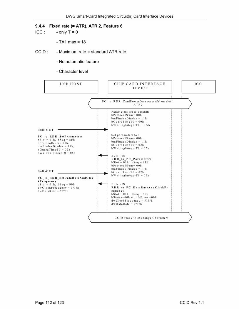
DWG Smart-Card Integrated Circuit(s) Card Interface Devices 9.4.4 Fixed rate (= ATR), ATR 2, Feature 6 ICC : - only T = 0 - TA1 max = 18 CCID : - Maximum rate = standard ATR rate - No automatic feature - Character level
U S B H O S T C H IP C A R D IN T E R F A C ED E V IC E
B u lk - INR D R _ to _ P C _ P a ra m e te r sb S lo t = 0 1 h , b S eq = 8 F hb P ro to c o lN u m = 0 0 hb m F in d ex D in d ex = 1 1 hb G u a rd T im eT 0 = 0 2 hb W a itin g In teg erT 0 = 0 5 h
IC C
B u lk -O U T
P C _ to _ R D R _ S e tP a r a m e te r sb S lo t = 0 1 h , b S eq = 8 F hb P ro to c o lN u m = 0 0 h ,b m F in d ex D in d ex = 1 1 h ,b G u a rd T im eT 0 = 0 2 hb W a itin g In teg erT 0 = 0 5 h
P a ra m ete rs se t to d e fa u lt:b P ro to c o lN u m = 0 0 hb m F in d ex D in d ex = 1 1 hb G u a rd T im eT 0 = 0 0 hb W a itin g In teg erT 0 = 0 A h
P C _ to _ R D R _ C a rd P o w erO n su c c ess fu l o n s lo t 1A T R 2
C C ID rea d y to ex c h a n g e C h a rac te rs
S e t p a ram ete rs to :b P ro to c o lN u m = 0 0 hb m F in d ex D in d ex = 1 1 hb G u a rd T im eT 0 = 0 2 hb W a itin g In teg erT 0 = 0 5 h
B u lk - INR D R _ to _ P C _ D a ta R a te A n d C lo c k F re q u e n cyb S lo t = 0 1 h , b S eq = 9 0 hb S ta tu s= 0 0 h w ith b E rro r = 0 0 hd w C lo c k F req u en c y = ????hd w D a ta R a te = ??? ?h
B u lk -O U T
P C _ to _ R D R _ S e tD a ta R a te A n d C lo ck F r e q u e n c yb S lo t = 0 1 h , b S eq = 9 0 hd w C lo c k F req u en c y = ????hd w D a ta R a te = ??? ?h
Page 112 of 123 CCID Rev 1.1
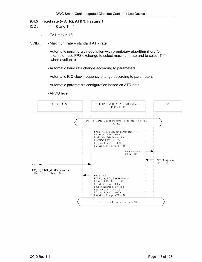
DWG Smart-Card Integrated Circuit(s) Card Interface Devices 9.4.5 Fixed rate (= ATR), ATR 3, Feature 1 ICC : - T = 0 and T = 1
- - TA1 max = 18 CCID : - Maximum rate = standard ATR rate
- Automatic parameters negotiation with proprietary algorithm (here for example : use PPS exchange to select maximum rate and to select T=1 when available)
- Automatic baud rate change according to parameters - Automatic ICC clock frequency change according to parameters - Automatic parameters configuration based on ATR data - APDU level
U S B H O S T C H IP C A R D IN T E R F A C ED E V IC E
B u lk - INR D R _ to _ P C _ P a ra m e te r sb S lo t = 0 1 h , b S eq = 9 2 hb P ro to c o lN u m = 0 1 hb m F in d ex D in d ex = 1 1 hb m T C C K S T 1 = 1 0 hb G u a rd T im eT 1 = 0 2 hb W a itin g In teg ers T 1 = 3 8 h
IC C
B u lk -O U T
P C _ to _ R D R _ G e tP a r a m e te r sb S lo t = 0 1 h , b S eq = 9 2 h
F ro m A T R d a ta , se t p a ra m ete rs to :b P ro to c o lN u m = 0 1 hb m F in d ex D in d ex = 1 1 hb m T C C K S T 1 = 1 0 hb G u a rd T im eT 1 = 0 2 hb W a itin g In teg ers T 1 = 3 8 h
P C _ to _ R D R _ C a rd P o w erO n su c c ess fu l o n s lo t 1A T R 3
C C ID rea d y to ex c h a n g e A P D U
P P S R esp o n se :F F 0 1 F E
P P S R eq u es t:F F 0 1 F E
CCID Rev 1.1 Page 113 of 123
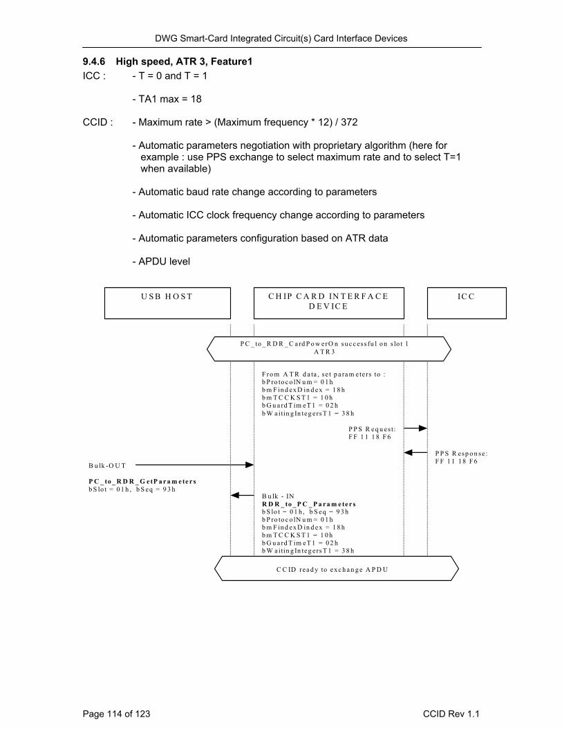
DWG Smart-Card Integrated Circuit(s) Card Interface Devices 9.4.6 High speed, ATR 3, Feature1 ICC : - T = 0 and T = 1 - TA1 max = 18 CCID : - Maximum rate > (Maximum frequency * 12) / 372
- Automatic parameters negotiation with proprietary algorithm (here for example : use PPS exchange to select maximum rate and to select T=1 when available)
- Automatic baud rate change according to parameters - Automatic ICC clock frequency change according to parameters - Automatic parameters configuration based on ATR data - APDU level
U S B H O S T C H IP C A R D IN T E R F A C ED E V IC E
B u lk - INR D R _ to _ P C _ P a ra m e te r sb S lo t = 0 1 h , b S eq = 9 3 hb P ro to c o lN u m = 0 1 hb m F in d ex D in d ex = 1 8 hb m T C C K S T 1 = 1 0 hb G u a rd T im eT 1 = 0 2 hb W a itin g In teg ers T 1 = 3 8 h
IC C
B u lk -O U T
P C _ to _ R D R _ G e tP a r a m e te r sb S lo t = 0 1 h , b S eq = 9 3 h
F ro m A T R d a ta , se t p a ra m ete rs to :b P ro to c o lN u m = 0 1 hb m F in d ex D in d ex = 1 8 hb m T C C K S T 1 = 1 0 hb G u a rd T im eT 1 = 0 2 hb W a itin g In teg ers T 1 = 3 8 h
P C _ to _ R D R _ C a rd P o w erO n su c c ess fu l o n s lo t 1A T R 3
C C ID rea d y to ex c h a n g e A P D U
P P S R esp o n se :F F 1 1 1 8 F 6
P P S R eq u es t:F F 1 1 1 8 F 6
Page 114 of 123 CCID Rev 1.1
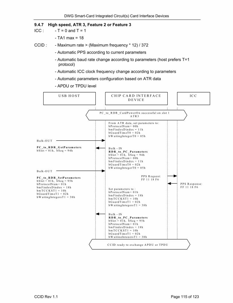
DWG Smart-Card Integrated Circuit(s) Card Interface Devices 9.4.7 High speed, ATR 3, Feature 2 or Feature 3 ICC : - T = 0 and T = 1
- TA1 max = 18
CCID : - Maximum rate > (Maximum frequency * 12) / 372
- Automatic PPS according to current parameters
- Automatic baud rate change according to parameters (host prefers T=1 protocol)
- Automatic ICC clock frequency change according to parameters
- Automatic parameters configuration based on ATR data
- APDU or TPDU level
U S B H O S T C H IP C A R D IN T E R F A C ED E V IC E
B u lk - INR D R _ to _ P C _ P a ra m e te r sb S lo t = 0 1 h , b S eq = 9 4 hb P ro to c o lN u m = 0 0 hb m F in d ex D in d ex = 1 1 hb G u a rd T im eT 0 = 0 2 hb W a itin g In teg erT 0 = 0 5 h
IC C
B u lk -O U T
P C _ to _ R D R _ G e tP a r a m e te r sb S lo t = 0 1 h , b S eq = 9 4 h
F ro m A T R d a ta , se t p a ra m ete rs to :b P ro to c o lN u m = 0 0 hb m F in d ex D in d ex = 1 1 hb G u a rd T im eT 0 = 0 2 hb W a itin g In teg erT 0 = 0 5 h
P C _ to _ R D R _ C a rd P o w erO n su c c ess fu l o n s lo t 1A T R 3
C C ID rea d y to ex c h a n g e A P D U o r T P D U
P P S R esp o n se :F F 1 1 1 8 F 6
P P S R eq u es t:F F 1 1 1 8 F 6
B u lk - INR D R _ to _ P C _ P a ra m e te r sb S lo t = 0 1 h , b S eq = 9 5 hb P ro to c o lN u m = 0 1 hb m F in d ex D in d ex = 1 8 hb m T C C K S T 1 = 1 0 hb G u a rd T im eT 1 = 0 2 hb W a itin g In teg ers T 1 = 3 8 h
B u lk -O U T
P C _ to _ R D R _ S e tP a r a m e te r sb S lo t = 0 1 h , b S eq = 9 5 hb P ro to c o lN u m = 0 1 hb m F in d ex D in d ex = 1 8 hb m T C C K S T 1 = 1 0 hb G u a rd T im eT 1 = 0 2 hb W a itin g In teg ers T 1 = 3 8 h
S e t p a ram ete rs to :b P ro to c o lN u m = 0 1 hb m F in d ex D in d ex = 1 8 hb m T C C K S T 1 = 1 0 hb G u a rd T im eT 1 = 0 2 hb W a itin g In teg ers T 1 = 3 8 h
CCID Rev 1.1 Page 115 of 123
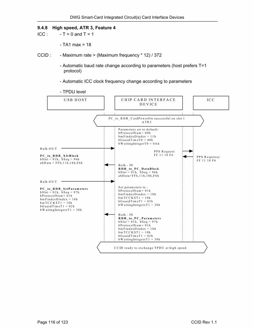
DWG Smart-Card Integrated Circuit(s) Card Interface Devices 9.4.8 High speed, ATR 3, Feature 4 ICC : - T = 0 and T = 1 - TA1 max = 18 CCID : - Maximum rate > (Maximum frequency * 12) / 372 - Automatic baud rate change according to parameters (host prefers T=1
protocol) - Automatic ICC clock frequency change according to parameters - TPDU level
U S B H O S T C H IP C A R D IN T E R F A C ED E V IC E
B u lk - INR D R _ to _ P C _ D a ta B lo c kb S lo t = 0 1 h , b S eq = 9 6 ha b D ata= F F h ,1 1 h ,1 8 h ,F 6 h
IC C
B u lk -O U T
P C _ to _ R D R _ X frB lo c kb S lo t = 0 1 h , b S eq = 9 6 ha b D ata = F F h ,1 1 h ,1 8 h ,F 6 h
P a ra m ete rs se t to d e fa u lt:b P ro to c o lN u m = 0 0 hb m F in d ex D in d ex = 1 1 hb G u a rd T im eT 0 = 0 0 hb W a itin g In teg erT 0 = 0 A h
P C _ to _ R D R _ C a rd P o w erO n su c c ess fu l o n s lo t 1A T R 3
C C ID rea d y to ex c h a n g e T P D U a t h ig h sp eed
P P S R esp o n se :F F 1 1 1 8 F 6
P P S R eq u es t:F F 1 1 1 8 F 6
B u lk - INR D R _ to _ P C _ P a ra m e te r sb S lo t = 0 1 h , b S eq = 9 7 hb P ro to c o lN u m = 0 1 hb m F in d ex D in d ex = 1 8 hb m T C C K S T 1 = 1 0 hb G u a rd T im eT 1 = 0 2 hb W a itin g In teg ers T 1 = 3 8 h
B u lk -O U T
P C _ to _ R D R _ S e tP a r a m e te r sb S lo t = 0 1 h , b S eq = 9 7 hb P ro to c o lN u m = 0 1 hb m F in d ex D in d ex = 1 8 hb m T C C K S T 1 = 1 0 hb G u a rd T im eT 1 = 0 2 hb W a itin g In teg ers T 1 = 3 8 h
S e t p a ram ete rs to :b P ro to c o lN u m = 0 1 hb m F in d ex D in d ex = 1 8 hb m T C C K S T 1 = 1 0 hb G u a rd T im eT 1 = 0 2 hb W a itin g In teg ers T 1 = 3 8 h
Page 116 of 123 CCID Rev 1.1
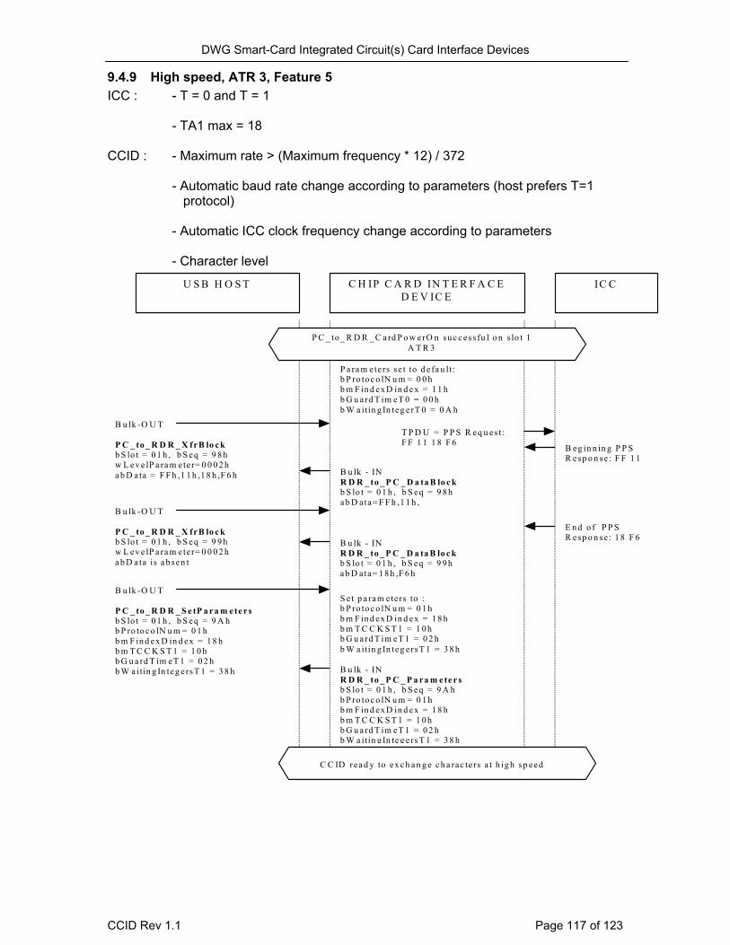
DWG Smart-Card Integrated Circuit(s) Card Interface Devices 9.4.9 High speed, ATR 3, Feature 5 ICC : - T = 0 and T = 1 - TA1 max = 18 CCID : - Maximum rate > (Maximum frequency * 12) / 372 - Automatic baud rate change according to parameters (host prefers T=1
protocol) - Automatic ICC clock frequency change according to parameters - Character level
U S B H O S T C H IP C A R D IN T E R F A C ED E V IC E
B u lk - INR D R _ to _ P C _ D a ta B lo c kb S lo t = 0 1 h , b S eq = 9 8 ha b D ata= F F h ,1 1 h ,
IC C
B u lk -O U T
P C _ to _ R D R _ X frB lo c kb S lo t = 0 1 h , b S eq = 9 8 hw L e v e lP a ra m ete r= 0 0 0 2 ha b D ata = F F h ,1 1 h ,1 8 h ,F 6 h
P a ra m ete rs se t to d e fa u lt:b P ro to c o lN u m = 0 0 hb m F in d ex D in d ex = 1 1 hb G u a rd T im eT 0 = 0 0 hb W a itin g In teg erT 0 = 0 A h
P C _ to _ R D R _ C a rd P o w erO n su c c ess fu l o n s lo t 1A T R 3
C C ID rea d y to ex c h a n g e c h a rac te rs a t h ig h sp eed
B eg in n in g P P SR esp o n se : F F 1 1
T P D U = P P S R eq u es t:F F 1 1 1 8 F 6
B u lk - INR D R _ to _ P C _ P a ra m e te r sb S lo t = 0 1 h , b S eq = 9 A hb P ro to c o lN u m = 0 1 hb m F in d ex D in d ex = 1 8 hb m T C C K S T 1 = 1 0 hb G u a rd T im eT 1 = 0 2 hb W a itin g In teg ers T 1 = 3 8 h
B u lk -O U T
P C _ to _ R D R _ S e tP a r a m e te r sb S lo t = 0 1 h , b S eq = 9 A hb P ro to c o lN u m = 0 1 hb m F in d ex D in d ex = 1 8 hb m T C C K S T 1 = 1 0 hb G u a rd T im eT 1 = 0 2 hb W a itin g In teg ers T 1 = 3 8 h
S e t p a ram ete rs to :b P ro to c o lN u m = 0 1 hb m F in d ex D in d ex = 1 8 hb m T C C K S T 1 = 1 0 hb G u a rd T im eT 1 = 0 2 hb W a itin g In teg ers T 1 = 3 8 h
E n d o f P P SR esp o n se : 1 8 F 6
B u lk -O U T
P C _ to _ R D R _ X frB lo c kb S lo t = 0 1 h , b S eq = 9 9 hw L e v e lP a ra m ete r= 0 0 0 2 ha b D ata is a b sen t
B u lk - INR D R _ to _ P C _ D a ta B lo c kb S lo t = 0 1 h , b S eq = 9 9 ha b D ata= 1 8 h ,F 6 h
CCID Rev 1.1 Page 117 of 123
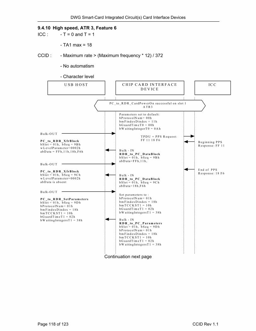
DWG Smart-Card Integrated Circuit(s) Card Interface Devices 9.4.10 High speed, ATR 3, Feature 6 ICC : - T = 0 and T = 1 - TA1 max = 18 CCID : - Maximum rate > (Maximum frequency * 12) / 372 - No automatism - Character level
U S B H O S T C H IP C A R D IN T E R F A C E D E V IC E
B u lk - IN R D R _ to _ P C _ D a ta B lo c k b S lo t = 0 1 h , b S e q = 9 B h a b D a ta = F F h ,1 1 h ,
IC C
B u lk -O U T P C _ to _ R D R _ X fr B lo c k b S lo t = 0 1 h , b S e q = 9 B h w L e v e lP a ra m e te r= 0 0 0 2 h a b D a ta = F F h ,1 1 h ,1 8 h ,F 6 h
P a ra m e te rs se t to d e fa u lt: b P ro to c o lN u m = 0 0 h b m F in d e x D in d e x = 1 1 h b G u a rd T im e T 0 = 0 0 h b W a itin g In te g e rT 0 = 0 A h
P C _ to _ R D R _ C a rd P o w e rO n su c c e ss fu l o n s lo t 1 A T R 3
B e g in n in g P P S R e sp o n se : F F 1 1
T P D U = P P S R e q u e s t: F F 1 1 1 8 F 6
B u lk - IN R D R _ to _ P C _ P a r a m e te r s b S lo t = 0 1 h , b S e q = 9 D h b P ro to c o lN u m = 0 1 h b m F in d e x D in d e x = 1 8 h b m T C C K S T 1 = 1 0 h b G u a rd T im e T 1 = 0 2 h b W a itin g In te g e rsT 1 = 3 8 h
B u lk -O U T P C _ to _ R D R _ S e tP a r a m e te r s b S lo t = 0 1 h , b S e q = 9 D h b P ro to c o lN u m = 0 1 h b m F in d e x D in d e x = 1 8 h b m T C C K S T 1 = 1 0 h b G u a rd T im e T 1 = 0 2 h b W a itin g In te g e rsT 1 = 3 8 h
S e t p a ra m e te rs to : b P ro to c o lN u m = 0 1 h b m F in d e x D in d e x = 1 8 h b m T C C K S T 1 = 1 0 h b G u a rd T im e T 1 = 0 2 h b W a itin g In te g e rsT 1 = 3 8 h
E n d o f P P S R e sp o n se : 1 8 F 6
B u lk -O U T P C _ to _ R D R _ X fr B lo c k b S lo t = 0 1 h , b S e q = 9 C h w L e v e lP a ra m e te r= 0 0 0 2 h a b D a ta is a b se n t
B u lk - IN R D R _ to _ P C _ D a ta B lo c k b S lo t = 0 1 h , b S e q = 9 C h a b D a ta = 1 8 h ,F 6 h
Continuation next page
Page 118 of 123 CCID Rev 1.1

DWG Smart-Card Integrated Circuit(s) Card Interface Devices
Continuation previous page
U S B H O S T C H IP C A R D IN T E R F A C E D E V IC E
IC C
C C ID re a d y to e x c h a n g e C h a ra c te rs a t h ig h sp e e d
B u lk - IN R D R _ to _ P C _ D a ta R a te A n d C lo c k F re q u e n c y b S lo t = 0 1 h , b S e q = 9 E h b S ta tu s= 0 0 h w ith b E rro r = 0 0 h d w C lo c k F re q u e n c y = ? ? ? ? h d w D a ta R a te = ? ? ? ? h
B u lk -O U T P C _ to _ R D R _ S e tD a ta R a te A n d C lo ck F r e q u e n c y b S lo t = 0 1 h , b S e q = 9 E h d w C lo c k F re q u e n c y = ? ? ? ? h d w D a ta R a te = ? ? ? ? h
CCID Rev 1.1 Page 119 of 123

DWG Smart-Card Integrated Circuit(s) Card Interface Devices 9.4.11 High speed, “EMV like”, Cold ATR: ATR1, Warm ATR: ATR4, Feature 1 ICC : - class AB (5v / 3v) - Cold ATR : negotiable mode, only T = 0, TA1 max = 18 - Warm ATR : specific mode, T = 1, TA1 = 18
CCID : - Automatic ICC activation on insertion - Automatic voltage selection - class A - Maximum rate > (Maximum frequency * 12) / 372 - Automatic parameters negotiation with proprietary algorithm (here “EMV
like”: try warm reset when ATR rejected because not EMV) - Automatic baud rate change according to parameters - Automatic ICC clock frequency change according to parameters - Automatic parameters configuration based on ATR data - APDU level
U S B H O S T C H IP C A R D IN T E R F A C ED E V IC E
IC C
B u lk - INR D R _ to _ P C _ D a ta B lo c kb S lo t = 0 1 h , b S eq = A 0 hb S ta tu s= 0 0 h w ith b E rro r = 0 0 hd w L en g th – len g th o f ab D a ta f ie lda b D ata = A T R 4
B u lk - INR D R _ to _ P C _ P a ra m e te r sb S lo t = 0 1 h , b S eq = A 1 hb P ro to c o lN u m = 0 1 hb m F in d ex D in d ex = 1 8 hb G u a rd T im eT 1 = 0 2 hb W a itin g In teg ers T 1 = 3 8 h
B u lk -O U T
P C _ to _ R D R _ Ic c P o w er O nb S lo t = 0 1 h , b S eq = A 0 hd w L en g th = 0 0 0 0 0 0 0 0 hb P o w e rS e lec t= 0 1 h
B u lk -O U T
P C _ to _ R D R _ G e tP a r a m e te r sb S lo t = 0 1 h , b S eq = A 1 h
Ic c In se rtedC o ld rese t IC C 5 V
A T R 1A T R re jec ted : W a rm res e t IC C 5 V
A T R 4F ro m A T R d a ta , se t p a ra m ete rs to :b P ro to c o lN u m = 0 1 hb m T C C K S T 1 = 1 0 hb G u a rd T im eT 1 = 0 2 hb W a itin g In teg ers T 1 = 3 8 h
In te rru p t - INR D R _ to _ P C _ N o tify S lo tC h a n g eb m S lo tIC C S ta te = x x x x 1 1 x x b
Page 120 of 123 CCID Rev 1.1
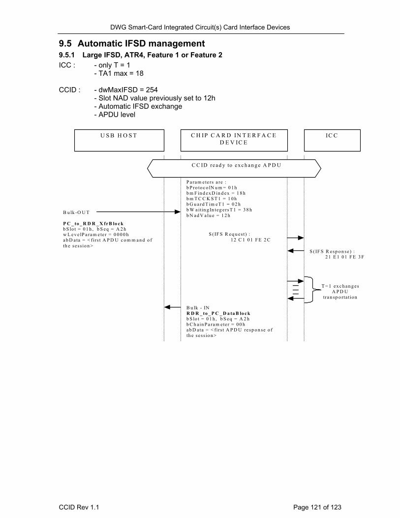
DWG Smart-Card Integrated Circuit(s) Card Interface Devices
9.5 Automatic IFSD management 9.5.1 Large IFSD, ATR4, Feature 1 or Feature 2 ICC : - only T = 1 - TA1 max = 18 CCID : - dwMaxIFSD = 254 - Slot NAD value previously set to 12h - Automatic IFSD exchange - APDU level
U S B H O S T C H IP C A R D IN T E R F A C ED E V IC E
B u lk - INR D R _ to _ P C _ D a ta B lo c kb S lo t = 0 1 h , b S eq = A 2 hb C h a in P a ra m ete r = 0 0 ha b D ata = < firs t A P D U resp o n se o fth e sess io n >
IC C
B u lk -O U T
P C _ to _ R D R _ X frB lo c kb S lo t = 0 1 h , b S eq = A 2 hw L e v e lP a ra m ete r = 0 0 0 0 ha b D ata = < firs t A P D U c o m m a n d o fth e sess io n >
P a ra m ete rs a re :b P ro to c o lN u m = 0 1 hb m F in d ex D in d ex = 1 8 hb m T C C K S T 1 = 1 0 hb G u a rd T im eT 1 = 0 2 hb W a itin g In teg ers T 1 = 3 8 hb N ad V a lu e = 1 2 h
C C ID re ad y to ex c h a n g e A P D U
S (IF S R esp o n se) : 2 1 E 1 0 1 F E 3 F
S (IF S R eq u es t) : 1 2 C 1 0 1 F E 2 C
T = 1 ex c h an g esA P D U
tra n sp o rta t ion
CCID Rev 1.1 Page 121 of 123

DWG Smart-Card Integrated Circuit(s) Card Interface Devices 9.5.2 Large IFSD, ATR4, Feature 4 ICC : - only T = 1 - TA1 max = 18 CCID : - dwMaxIFSD = 254 - Slot NAD value previously set to 12h - Automatic IFSD exchange - TPDU level
U S B H O S T C H IP C A R D IN T E R F A C ED E V IC E
B u lk - INR D R _ to _ P C _ D a ta B lo c kb S lo t = 0 1 h , b S eq = A 3 hb C h a in P a ra m ete r = 0 0 ha b D ata = < T P D U resp o n se>
IC C
B u lk -O U T
P C _ to _ R D R _ X frB lo c kb S lo t = 0 1 h , b S eq = A 3 hw L e v e lP a ra m ete r = 0 0 0 0 ha b D ata = < firs t T P D U c o m m a n d o fth e sess io n >
P a ra m ete rs a re :b P ro to c o lN u m = 0 1 hb m F in d ex D in d ex = 1 8 hb m T C C K S T 1 = 1 0 hb G u a rd T im eT 1 = 0 2 hb W a itin g In teg ers T 1 = 3 8 hb N ad V a lu e = 1 2 h
C C ID rea d y to e x ch an g e T P D U
S (IF S R esp o n se) : 2 1 E 1 0 1 F E 3 F
S (IF S R eq u es t) : 1 2 C 1 0 1 F E 2 C
< T P D U resp o n se>
< firs t T P D U c o m m an d o f th e se ss io n >
Page 122 of 123 CCID Rev 1.1

DWG Smart-Card Integrated Circuit(s) Card Interface Devices
Notes:
CCID Rev 1.1 Page 123 of 123