Embed Size (px)
Citation preview

TEA19051BTKUSB-PD 2.0/USB-PD 3.0/QC 2.0/QC 3.0/QC 4 (+) controller forSMPSRev. 3 — 21 January 2019 Product data sheet
1 General description
The TEA19051BTK is a highly configurable secondary side SMPS controller that isavailable in many factory configured versions. Section 15 gives an overview of the off-the-shelf available versions of the TEA19051BTK. To inquire about the possibilities ofcustomer-specific versions, contact your local sales representative.
The TEA19051BTK supports the following protocols:
• USB Type-C v.1.3• USB power delivery (USB-PD) including programmable power supply (PPS)• Battery Charging 1.2 (BC1.2)• Qualcomm® QuickCharge™ QC2.0, QC3.0, and QC4+
A complete smart-charging switch mode power supply (SMPS) can be built incombination with the TEA193x primary controller and the TEA199x secondary sidesynchronous rectifier (SR) controller.
The TEA19051BTK can be provided in several small packages with low pin count. Dueto its small number of external components, a small form factor SMPS can be built thatmeets efficiency requirements like CoC Tier-2, EuP Iot6, and DOE v6 with an extremelyno-load power (< 30 mW).
The TEA19051BTK has a high level of digital integration. It incorporates all requiredcircuits, including a charge pump to drive an external NMOS load switch directly, a USB-PD physical interface (PHY), and an integrated driver for fast output discharge.
The output voltage and output current are continuously measured and are used to controlthe SMPS. Two GPIO pins measure the adapter temperature and the temperature in thecable/connector. Optionally, the GPIO pins can be used for other features, like supply(see Table 4). The die temperature of the TEA19051BTK is monitored via an internaltemperature sensor.
Multiple protections ensure the best-in-class charging safety for the TEA19051BTK.
To ensure correct operation under all conditions, all protections except UVP areimplemented in hardware. The response of these protections can be programmedas latched or safe restart. Although not recommended, these protections can also bedisabled individually via the settings in the non-volatile multi-time programmable (MTP)memory.
If an output short circuit occurs, the power dissipation in the adapter can be below50 mW.
For output voltage regulation, current regulation, and protection, only a singleoptocoupler is required in the application.
The TEA19051BTK operates in CV mode with a better than 2 % voltage accuracy. In CCmode, it operates with a better than 2 % full-load current accuracy.

NXP Semiconductors TEA19051BTKUSB-PD 2.0/USB-PD 3.0/QC 2.0/QC 3.0/QC 4 (+) controller for SMPS
TEA19051BTK All information provided in this document is subject to legal disclaimers. © NXP B.V. 2019. All rights reserved.
Product data sheet Rev. 3 — 21 January 20192 / 60
2 Features and benefits
2.1 General
• Best-in-class fail-safe application for high-power adapters; gives complete protectionagainst overload conditions in the load (e.g. phone)
• Wide output voltage operating range (2.9 V to 21 V)• Ultra-high efficiency together with TEA193x QR/DCM controller and TEA199x SR
controller• Very low no-load power (< 30 mW for the complete system solution)• High power density• Dedicated SW pin to drive external NMOS directly• Constant voltage (CV) and constant current (CC) control (programmable level)• Precise voltage and current control with low minimum step size (voltage 12-bit DAC,
current 10-bit DAC)• Continuous measurement of output voltage and output current with a better than 2 %
accuracy• Low-cost HVSON16 package (suitable for reflow soldering)• Low-cost bill of materials (BOM; ≈15 external components)• Embedded MCU (with ROM, RAM, and MTP memory)• Discharge pin for fast output voltage ramp down• Built-in series regulator and programmable cable compensation• Non-volatile MTP memory for storage of system configuration parameters
2.2 Protocol support
• USB Type-C v.1.3• USB power delivery (USB-PD) 2.0 and 3.0 including programmable power supply
(PPS)• Qualcomm® QuickCharge™ QC2.0, QC3.0, and QC4+ protocols• Battery Charging 1.2 (BC 1.2)• Unstructured vendor defined messages (VDMs), which can be used for MTP
programming, e.g. to get Vendor IDs

NXP Semiconductors TEA19051BTKUSB-PD 2.0/USB-PD 3.0/QC 2.0/QC 3.0/QC 4 (+) controller for SMPS
TEA19051BTK All information provided in this document is subject to legal disclaimers. © NXP B.V. 2019. All rights reserved.
Product data sheet Rev. 3 — 21 January 20193 / 60
2.3 Protections
• Overtemperature protection (OTP): one internal and two external• Adaptive overvoltage protection (OVP)• Adaptive undervoltage protection (UVP)• Overcurrent protection (OCP)• Undervoltage lockout (UVLO) protection• Output short protection (OSP)• Open-supply protection (OSUP)• Open-ground protection (OGP)• Overvoltage protection DP, DM, CC1, and CC2 pins• Soft short protection at the CC1 and CC2 pins• Soft short protection at the output
To ensure safe operation, the TEA19051BTK switches off the load during faultconditions.
3 Applications
• USB chargers for smart phones and tablets supporting the Qualcomm® QuickCharge™
QC2.0, QC3.0, and QC4+ protocols• USB-PD 3.0, type C 1.3 chargers with optional VDM support for smartphones and
tablets

NXP Semiconductors TEA19051BTKUSB-PD 2.0/USB-PD 3.0/QC 2.0/QC 3.0/QC 4 (+) controller for SMPS
TEA19051BTK All information provided in this document is subject to legal disclaimers. © NXP B.V. 2019. All rights reserved.
Product data sheet Rev. 3 — 21 January 20194 / 60
4 Ordering informationTable 1. Ordering information
PackageType number
Name Description Version
TEA19051BAATK/1
TEA19051BABTK/1
TEA19051BACTK/1
TEA19051BAFTK/1
TEA19051BAGTK/1
TEA19051BAHTK/1
TEA19051BAKTK/1
TEA19051BAMTK/1
TEA19051BAPTK/1
TEA19051BARTK/1
HVSON16 plastic small enhanced very thin small outline package; no leads; 16terminals; body: 3.5 × 5.5 × 0.85 mm
SOT1308-1
5 MarkingTable 2. MarkingType number Marking code
TEA19051BAATK A19051BAA
TEA19051BABTK A19051BAB
TEA19051BACTK A19051BAC
TEA19051BAFTK A19051BAF
TEA19051BAGTK A19051BAG
TEA19051BAHTK A19051BAH
TEA19051BAKTK A19051BAK
TEA19051BAMTK A19051BAM
TEA19051BAPTK A19051BAP
TEA19051BARTK A19051BAR

NXP Semiconductors TEA19051BTKUSB-PD 2.0/USB-PD 3.0/QC 2.0/QC 3.0/QC 4 (+) controller for SMPS
TEA19051BTK All information provided in this document is subject to legal disclaimers. © NXP B.V. 2019. All rights reserved.
Product data sheet Rev. 3 — 21 January 20195 / 60
6 Block diagram
VCC
SW
DISCH
aaa-025896
PARAMETERMTP
CHARGEPUMP
VOUT_below_0p8
Vout_below_vcc
I2C(M/S)
BG_det
SW_OFF SUPPLYBLOCK
BG_OK
RAM
OSC
OR
OVP
UVLO
OTP
SW_OFF
ROM
SCL SDA
µC
ana_ctrl
ana_
ctrl
DAC
DIGITAL
amp
CCmode
USB-PDPHY
TYPECCONDET
USB-PDPROTO
USBBLOCK
GND
GPIO2
SGND
ISNS
DM
DP
CC2
CC1
EDP
OVP
OVP
OVP
ADC
ADC
DAC
DAC
DAC
DAC AD
C
GPIO1
OPTO
VSNS
4 bits
REF
UVLO
30 µA
3 levels+ off
3 levels+ off
3.3 V
BG_OK
VCC_below_xxx
OVP
OCP
20 mA
0.8 V
3.3 V
3.3 V
3.3 V
Figure 1. TEA19051BTK block diagram

NXP Semiconductors TEA19051BTKUSB-PD 2.0/USB-PD 3.0/QC 2.0/QC 3.0/QC 4 (+) controller for SMPS
TEA19051BTK All information provided in this document is subject to legal disclaimers. © NXP B.V. 2019. All rights reserved.
Product data sheet Rev. 3 — 21 January 20196 / 60
7 Pinning information
7.1 Pinning
16
IC
9
1
8
107
116
125
134
143
15
SW
SDA
17 EDP DM
DP
CC2
CC1
DISCH
GND2
VCC
SCL
VSNS
GPIO2
ISNS
GPIO1
SGND
OPTO
aaa-025739
Figure 2. TEA19051BTK pinning diagram (SOT1308-1)
7.2 Pin description
Table 3. Pin descriptionSymbol Pin Description
VCC 1 supply voltage
OPTO 2 OPTO driver
SGND 3 sense ground
GPIO1 4 general-purpose input/output
ISNS 5 current sense input
GPIO2 6 general-purpose input/output
VSNS 7 voltage sense input
SCL 8 I2C clock line
SDA 9 I2C data line
DM 10 negative terminal of the data communication line
DP 11 positive terminal of the data communication line
CC2 12 type C CC2 line detection and USB-PD communication
CC1 13 type C CC1 line detection and USB-PD communication
DISCH 14 fast discharge sink
GND 15 ground
SW 16 NMOS gate drive output
EDP 17 exposed die pad

NXP Semiconductors TEA19051BTKUSB-PD 2.0/USB-PD 3.0/QC 2.0/QC 3.0/QC 4 (+) controller for SMPS
TEA19051BTK All information provided in this document is subject to legal disclaimers. © NXP B.V. 2019. All rights reserved.
Product data sheet Rev. 3 — 21 January 20197 / 60
8 Functional description
The TEA19051BTK can be considered as a versatile programmable replacement for thewell-known TL431 shunt regulator series, where:
• The VSNS pin takes the role of the REF input of the TL431• The OPTO pin takes the role of the cathode• The GND pin takes the role of the anode
In addition to the constant voltage (CV) mode, which is regulated via the VSNS pin, thesystem supports constant current (CC) mode. The current control loop is regulated andthe cable compensation is added via the ISNS pin.
Alternatively, the ISNS input can be used for overcurrent protection (OCP; see Table 4).Several other protections are available. Many of these protections are programmableas latched or safe restart. For guaranteed safety, all protections are implemented inhardware. So, even when the microcontroller stops, the protections are still functional.
The output voltage and the output current can be controlled via USB-PD using the CCpins. They can also be controlled via QC using the DP and DM pins.
The output current and the output voltage are continuously measured via an integratedAD-converter. The values can be made available continuously via the USB-PD protocol.The applied time constant of the digital filter is initialized via the firmware. A dedicatedsignal that indicates a stable output voltage/output current for a reliable measurement isavailable. It can be used, for example, to determine and monitor the cable resistance inthe portable device.
The external temperatures, measured via the GPIO1 and GPIO2 pins, are continuouslymonitored. From the GPIO voltages and applied currents, the controller calculates thecorresponding temperatures. These temperatures can be communicated to the portabledevice. Optionally, an OTP function is added to this external temperature measurement,which is programmable via MTP (see Table 4).
The available protections are implemented in hardware. They are independent ofprocessor actions. These protections in combination with the NMOS load switch ensure afully safe operation with only one optocoupler. When the optocoupler fails, the OVP of theprimary side controller (TEA1936x) limits the maximum output voltage.
The TEA19051BTK fully supports the type-C connector standard.
When a Type C receptacle is used, the CC1/CC2 pair is used for plug attach/detachdetection. It is also meant to support the USB-PD communication standard. The DP/DMpair is meant to support:
• Battery Charging 1.2• Qualcomm® QuickCharge™ QC2.0 and QC3.0
The USB-PD specification requires the use of a load switch and certain dischargebehavior of the output voltage at the connector Vbus. So, to drive the gate of an externalNMOS switch, the TEA19051BTK is equipped with an SW pin. To be able to dischargeVbus using an external resistor in series with an internal switch, the TEA19051BTK isequipped with a DISCH pin.
User-defined parameters can be stored in the non-volatile multi-time programmable(MTP) memory.

NXP Semiconductors TEA19051BTKUSB-PD 2.0/USB-PD 3.0/QC 2.0/QC 3.0/QC 4 (+) controller for SMPS
TEA19051BTK All information provided in this document is subject to legal disclaimers. © NXP B.V. 2019. All rights reserved.
Product data sheet Rev. 3 — 21 January 20198 / 60
8.1 Start-up and supply
The TEA19051BTK is supplied via the VCC pin connected to the secondary DC voltageof an AC-to-DC SMPS converter (see Figure 7). To control the primary side controller,this VCC voltage is regulated via an integrated voltage/current control loop with externalloop compensation and an external optocoupler. This optocoupler is part of the gain loopof the primary side SMPS controller.
At each start-up and after power-on reset, the optocoupler current is initially zero. So,the AC-to-DC converter starts up with full output power, resulting in a rapid increase ofthe VCC voltage. Due to the low VCC(start) level (≈3 V), the TEA19051BTK ensures thatit is fully operating before the VCC reaches the default initial regulation level. The defaultvalues of the initial regulation level are 5 V and 3 A and they are programmed in the non-volatile memory (MTP).
At power-on reset, the safe default values, which are read from MTP, are set.
When the VCC voltage is below the UVLO level, the external NMOS load switch is off.When the output is shorted while the load switch is closed, the UVLO is also triggered.The load switch is then immediately opened and the system restarts after the safe restarttimer.
When the VCC exceeds the UVLO level, all circuits, the initial DAC value, and theresistive divider ratio are initialized. The system regulates the output to 5 V with a limitedoutput current of 3 A. All these values can be set via the MTP.
To minimize the output voltage overshoot after start-up, an internal 20 mA current sinkis applied to VCC when the VCC voltage exceeds 1.05 × Vo(default). The sink currentremains active until the VCC voltage has dropped to below 1.05 × Vo(default) again.
After the output voltage has stabilized, the load switch becomes conducting and thesystem waits for an attach. Before the attach, only the essential circuits are workingwhich reduces the no-load power to its minimum.
When the voltage on one of the CC pins drops to below the VIH(Rd) level, an attach isdetected and all circuits are enabled.
If a protocol is detected, it is allowed to change the voltage and current.
5 V regulation
20 mAdischarge VCC
reading EEPROM
initialization
1.05 x Vo(default)
UVLO
aaa-023848
Figure 3. Start-up sequence
The TEA19051BTK operates on supply voltages up to 21 V. The voltage on the VCC pinis used to detect an OVP and UVP. The OVP and UVP level are set as a percentage ofthe requested output voltage level.

NXP Semiconductors TEA19051BTKUSB-PD 2.0/USB-PD 3.0/QC 2.0/QC 3.0/QC 4 (+) controller for SMPS
TEA19051BTK All information provided in this document is subject to legal disclaimers. © NXP B.V. 2019. All rights reserved.
Product data sheet Rev. 3 — 21 January 20199 / 60
If the supply voltage drops to below the UVLO level, the system returns to the no-supplystate and opens the load switch. Analog circuits are reset below UVLO. The internaldigital circuits are reset below the band gap voltage reference level.
8.2 Voltage loop
The analog constant voltage (CV) loop regulates VCC such that the voltage on theVSNS pin equals the internal reference voltage. An external resistor divider is connectedbetween VCC, the VSNS pin, and ground. The value of this divider must match thevalue that is programmed in MTP exactly. It depends on the maximum voltage in theapplication. The divider values are:
• 1/ 2.5; maximum PDO voltage ≤ 6 V• 1/5.476; maximum PDO voltage ≤ 13 V• 1/8.325; maximum PDO voltage ≤ 20 V• 1/8.828; maximum PDO voltage ≤ 21 V
The CV loop is regulated by varying the current through an optocoupler diode similarto a TL431 driven control loop commonly used in switch mode power supplies. The RCcombination between the OPTO and VSNS pin determines the dynamic behavior ofthe integrating part of the control loop. The resistor in series with the optocoupler diodedetermines the dynamic behavior of the proportional part of the control loop. To preventsaturation of the control loop during switching, a diode is placed in parallel to this resistor.See Section 13.3 for more information about the control loop.
When the voltage loop reference is set to a higher value using the USB-PD or the QCprotocol, the internal reference voltage is updated to the new setting within 20 μs. Theoutput voltage is regulated to the requested voltage with a speed determined by thecontrol loop. If there is a transition down, a predefined ramp down sequence is followedto prevent a high undershoot. Depending on the step size, the ramp down either followsa linear or a parabolic slope. For a transition up, no special measures are required toprevent an overshoot. The reason is that the charging current of the loop capacitor liftsthe voltage on the VSNS pin when the VCC voltage in the application increases.

NXP Semiconductors TEA19051BTKUSB-PD 2.0/USB-PD 3.0/QC 2.0/QC 3.0/QC 4 (+) controller for SMPS
TEA19051BTK All information provided in this document is subject to legal disclaimers. © NXP B.V. 2019. All rights reserved.
Product data sheet Rev. 3 — 21 January 201910 / 60
aaa-021703
VCC
OPTO
a. Circuit
aaa-021704
VCC
discharge
loop saturated
Vopto
b. Curve
Figure 4. Linear transition down (no load)
A linear ramp-down (see Figure 4) can yield a perfect linear ramp of the output voltagewithout any undershoot. However, depending on the loop bandwidth, the voltage loopcan end up in saturation. Saturation hampers a fast response to a load step immediatelyfollowing the end of the ramp (most protocols do not allow any load to be drawn duringa transition). Making the ramp down slower can prevent saturation of the loop. However,a slower ramp down can contradict with the maximum discharge time most protocolsspecify.
A parabolic discharge curve (see Figure 5; patent pending) initially causes the voltageloop to saturate, due to the initial rapid ramp down. However, it allows the loop to recoverand to resume regulation toward the end of the curve. The total parabolic sequence timemust be chosen such that no undershoot under the final end value occurs.

NXP Semiconductors TEA19051BTKUSB-PD 2.0/USB-PD 3.0/QC 2.0/QC 3.0/QC 4 (+) controller for SMPS
TEA19051BTK All information provided in this document is subject to legal disclaimers. © NXP B.V. 2019. All rights reserved.
Product data sheet Rev. 3 — 21 January 201911 / 60
aaa-021703
VCC
OPTO
a. Circuit
aaa-021705discharge
f(parabola factor)
loop saturated
loop reference
parabola depth
VCC
Vopto
b. Curve
Figure 5. Parabolic transition down (no-load)
8.3 Current loop
The voltage drop across a small external series resistor between the output returnterminal and the converter ground is supplied to the ISNS pin. An internal amplifiermultiplies the voltage on the ISNS pin by a factor of 50. The output voltage of theamplifier must remain below 2.5 V. The external resistor value can be chosen from 2 mΩup to 22.5 mΩ in steps of 0.02 mΩ. The external resistor value must correspond to theprogrammed value in MTP. Any deviation from this MTP value, e.g. due to PCB-layoutimperfections, causes a current error and must be corrected (see Section 13.2). Theground connection of the external sense resistor must be connected to the SGND pin viaan independent sense wire.
The combination of the maximum current in the application, the sense resistor, and thegain of the internal amplifier must be chosen such that the output voltage of the internalamplifier remains below 2.5 V.
When the application is used in CC-mode, an RC-combination must be connectedbetween the OPTO pin and the ISNS pin (see Section 13.4).

NXP Semiconductors TEA19051BTKUSB-PD 2.0/USB-PD 3.0/QC 2.0/QC 3.0/QC 4 (+) controller for SMPS
TEA19051BTK All information provided in this document is subject to legal disclaimers. © NXP B.V. 2019. All rights reserved.
Product data sheet Rev. 3 — 21 January 201912 / 60
8.4 Cable compensation
With cable compensation enabled, the output voltage is increased when the outputcurrent increases to compensate for the voltage drop over the cable. The value of thecable compensation is the same for all PDOs. It is set in MTP between the minimum andmaximum values (see Table 4).
Setting the cable compensation above 200 mV/A is not recommendable. The cablecompensation can be enabled/disabled for each individual PDO.
8.5 Load switch
A low-cost NMOS transistor is used as load switch between VCC and Vbus (see Figure 7).A dedicated switch-drive output pin (SW pin) controls this NMOS transistor. The output(high) level of the switch drive output is VCC + 6 V using an internal charge pump.
As long as VCC is below the UVLO level or if the VCC connection is open, the SW pin isheld low, ensuring that the load switch is off. To ensure that the NMOS is also kept offwhen the SW pin is disconnected, an external (high-ohmic) resistor is required betweenthe gate of the NMOS and Vbus.
To avoid charging VCC via the back-gate diode of the load switch, it is possible to applytwo NMOS switches in series, with their sources connected together.
8.6 Discharge function
The DISCH pin, which has an internal low-ohmic switch, provides the means to dischargethe output Vbus quickly. An external series resistor limits the maximum current and the ICdissipation.
To check if the output voltage has dropped to below 0.8 V, a comparator is implemented.This voltage drop is a requirement of the USB-PD specification (vSafe0V) if there is ahard reset.
When the internal DISCH switch is activated, the voltage at the DISCH pin is always low,because of the external current limiting resistor. A mechanism has been implementedto check the real output voltage. During a hard reset discharge sequence, when VCCis below vSafe5V, the switch is opened every millisecond for 20 μs to check the outputvoltage at the end of the 20 μs period. The check of the output voltage is done until thevoltage remains below 0.7 V and the hard reset discharge sequence is terminated. Forthis check to work properly, the capacitance on the DISCH pin and the external currentlimiting resistor must have a time constant that is short enough.

NXP Semiconductors TEA19051BTKUSB-PD 2.0/USB-PD 3.0/QC 2.0/QC 3.0/QC 4 (+) controller for SMPS
TEA19051BTK All information provided in this document is subject to legal disclaimers. © NXP B.V. 2019. All rights reserved.
Product data sheet Rev. 3 — 21 January 201913 / 60
To ensure that the output remains low, a 1 mA sink current is present on the DISCH pinwhen both the load switch and discharge switch are off. The period that the DISCH pinis active in unattached state (td(act)) is typically 100 ms. The reason for this limitation is toprevent that excessive power dissipation occurs if an external Vbus voltage is applied.
8.7 Detach detection
When the voltage on one of the CC pins is greater than 1.2 V, a detach is detected. Ifthe type C cable is disconnected, the output voltage is regulated to its default value (5 V)after 200 µs.
8.8 Internal temperature measurement
The internal die temperature is monitored continuously. Its value can be requested withthe appropriate vendor defined message (VDM). When the internal OTP (see Table 5) isenabled, the internal OTP is triggered when the die temperature exceeds the value that isprogrammed in MTP.
8.9 GPIO pins
The internal hardware of the GPIO1 and GPIO2 pins is identical.
In the MTP, the following functions can be selected for each GPIO pin:
• Off• NTC• NTC + OTP• Supply
In the sections below, the functions are further explained.
8.9.1 Off
The GPIO pin is disabled and can be connected to ground.
8.9.2 NTC
With the NTC function enabled, the GPIO pins can be used to measure the adapter andcable connector temperature via NTC resistors. The NTC connected to GPIO1 is meantfor measuring the (cable) connector temperature. The NTC connected to GPIO2 formeasuring the adapter temperature. The temperature values can be requested with theappropriate VDM command. To ensure an accurate temperature measurement over thecomplete temperature range, both external NTCs are supplied via an adaptive currentsource (see Figure 6).

NXP Semiconductors TEA19051BTKUSB-PD 2.0/USB-PD 3.0/QC 2.0/QC 3.0/QC 4 (+) controller for SMPS
TEA19051BTK All information provided in this document is subject to legal disclaimers. © NXP B.V. 2019. All rights reserved.
Product data sheet Rev. 3 — 21 January 201914 / 60
aaa-028134
DIGITALCONTROL
FIRMWARE USB-PD
ADCMTP
disable
OTP level
CC1CC2
GPIO
I3 = 240 µA
I2 = 60 µA
I1 = 15 µA
a. Circuit
Temperature-50 0 50
I1 = 15 µA I2 = 60 µA I3 = 240 µA
100 150
aaa-028135
1
2
3VGPIO
0
2.5
1.5
0.50.4
b. Curves
Figure 6. External NTC is supplied via adaptive current sources
The voltage at a GPIO pin is measured via an internal A-to-D converter. If the voltageon the GPIO pin drops to below 400 mV, the source current is increased. If the voltageon the GPIO pin exceeds 2.4 V, the source current is decreased. When a 47 kΩ NTCresistor with a Beta of 4108 is used, the temperature is accurately measured with a betterthan < 5 °C accuracy within a range of 0 °C to > 120 °C.

NXP Semiconductors TEA19051BTKUSB-PD 2.0/USB-PD 3.0/QC 2.0/QC 3.0/QC 4 (+) controller for SMPS
TEA19051BTK All information provided in this document is subject to legal disclaimers. © NXP B.V. 2019. All rights reserved.
Product data sheet Rev. 3 — 21 January 201915 / 60
8.9.3 NTC + OTP
With this function enabled, an OTP function is added to the NTC function. The OTPfunction is integrated in hardware. The OTP level is set in MTP.
When the NTC (+ OTP) function is enabled for a GPIO pin, but this GPIO pin is not usedin the application, it must be connected to ground via a fixed 47 kΩ resistor. Do not leavethe unused pin floating or connect it to ground.
8.9.4 Supply
When the supply functionality is chosen for the GPIO pin in MTP, the output of the GPIOcan be used to supply, e.g., an EEPROM. The following modes can be chosen via MTP:
• The supply signal is high continuously• Dynamic switching of the I2C slave supply on the GPIO pin.
When the master activates I2C communication, the supply is turned on first. After adelay, the I2C communications start. When I2C communications stops for 1 s, thesupply is turned off.
• The signal on the GPIO can have inverted behavior
8.10 Communication
If a type-C receptacle is used, attach/detach detection and USB-PD communication isprovided on the CC pins.
DP and DM provide the communication interface for QC2.0 and QC3.0.
If a type-A receptacle is used, attach/detach detection can be disabled (via MTP). Theload switch is closed (when no protection is triggered).
8.10.1 USB Type-C
The TEA19051BTK complies with the USB Type-C 1.3 specification (see Ref. 2) in thesense that the distinct pull-up current values support attach/detach and current capabilityadvertising. The attach/detach detection is done in the hardware. So, if there is a detach,a return of Vbus to vSafe5V is always ensured. The hardware implementation of thereturn of Vbus to vSafe5V eliminates the risk of software implementations where Vbus maystay at an unsafe level if the program execution stalls.
To support currents higher than 3 A, use a captive cable. Vconn is not supported.

NXP Semiconductors TEA19051BTKUSB-PD 2.0/USB-PD 3.0/QC 2.0/QC 3.0/QC 4 (+) controller for SMPS
TEA19051BTK All information provided in this document is subject to legal disclaimers. © NXP B.V. 2019. All rights reserved.
Product data sheet Rev. 3 — 21 January 201916 / 60
8.10.2 USB-PD
The TEA19051BTK supports the USB-PD, release 3.0 specification (see Ref. 4) as far asit is required for a DFP.
The TEA19051BTK supports the programmable power supply (PPS) part of the USB-PD3.0 specification.
The TEA19051BTK can be programmed such that it only complies with the USB-PD 2.0specification. With these MTP settings, power-brick USB-PD-2.0 testing can be done andUSB-PD 2.0 qualification is possible.
Maximum seven different power data objects (PDO) can be defined in the non-volatile memory (MTP). Released types have a predefined set of PDOs programmed(see Table 4). For each PDO, current limit type (OCP/CC) and cable compensation on/off can be set. However, any other voltage or current within the range can be defined in aPDO.
Four of the seven PDOs can be set as programmable power supply (PPS) instead of aFixed Power Supply via MTP.
The TEA19051BTK supports the QC4+ VDMs.
To make USB-PD certification possible, QC2.0 and QC3.0 must be disabled. DisablingQC2.0 and QC3.0 can be done in MTP or by not connecting the TEA19051BTK DP andDM pins. To pass BC1.2, the DP and DM pins of the connector must be connected toeach other.
8.10.3 Discover identification
The TEA19051BTK supports the discover identification protocol in USB-PD. It is possibleto program VID, PID, and BCD values in MTP. These values can be requested via VDMmessages.
The maximum power, which is used to determine the power profile, can be set in MTP.
8.10.4 Battery charging
The standard battery charging protocol is supported according to the BC1.2 specification(see Ref. 1).
8.10.5 Quick charge
The Qualcomm® QuickCharge™ QC2.0, QC3.0, and QC4+ protocols are fully supported(see Ref. 5, Ref. 6, and Ref. 7). The required fixed and PPS PDOs can be configured inMTP. The fixed PDO settings that are used for QC2.0 can be set via MTP.
When QC 3.0 is used, the voltage can be set via this protocol from 3.6 V to 12 V in stepsof 200 mV. The maximum voltage can be limited if wanted via MTP settings.

NXP Semiconductors TEA19051BTKUSB-PD 2.0/USB-PD 3.0/QC 2.0/QC 3.0/QC 4 (+) controller for SMPS
TEA19051BTK All information provided in this document is subject to legal disclaimers. © NXP B.V. 2019. All rights reserved.
Product data sheet Rev. 3 — 21 January 201917 / 60
8.10.6 MTP configuration
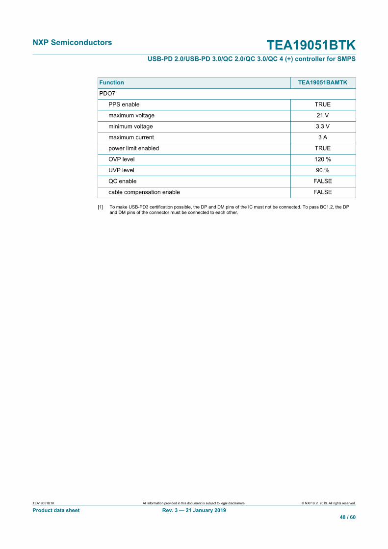
The TEA19051BTK is configurable via MTP. The different types are defined inSection 15. Table 4 gives an overview of the programmability with their minimum/maximum values.
Table 4. MTP configuration optionsFunction Options minimum
levelmaximum
levelstep size
default output voltage - 3 V 10 V 50 mV
default maximum output current - 0.3 A 5 A 20 mA
GPIO1 disable; NTC;NTC with OTP[1]; Supply
- - -
GPIO1 protection level - 62 °C 111 °C variable but< 5 °C
GPIO2 disable; NTC;NTC with OTP[1]; Supply
- - -
GPIO2 protection level - 62 °C 111 °C variable but< 5 °C
OTP internal - 27 °C 135 °C 4.3 °C
external sense resistor(Rsns) - 2 mΩ 22 mΩ 0.02 mΩ
external resistor divider VCC/VSNS (=DIV)[2]
8.325; 2.5; 5.476; 8.828 - - -
cable compensation[3] - 0 mV/A Rsns * DIV * 8V/A
variable
CC mode or OCP mode OCP-mode/CC-mode - - -
PDO1 5 V3 A
- - -
PDO2; PDO3; PDO4; PDO5;PDO6; PDO7
--
3 V0.3 A
20 V10 A
0.05 V0.01 A
OVP level (PDO)[4] 120 %; 125 %; 130 % - - -
UVP level (PDO)[4] off; 60 %; 70 %; 80 % - - -
UVP level (APDO)[4] off; 70 %; 80 %; 90 % - - -
PDO QC enable[4] TRUE/FALSE - - -
PDO PPS enable[5] TRUE/FALSE - - -
QC3.0 cable compensationenable
TRUE/FALSE - - -
QC3.0 maximum power - 0 W 102.3 W 0.1 W
USB3.0 enable TRUE/FALSE - - -
power limit PPS TRUE/FALSE - - -
minimum voltage APDO - 3.3 V 20 V -
[1] The NTC readout and OTP levels are defined with an NTC of 47 kΩ and a B-constant of 4108.[2] Maximum output voltage for 5.476 is 13 V. Maximum output voltage for 2.5 V is 6 V.[3] Cable compensation above 200 mV/A is not recommended.[4] Can be selected for each PDO individually.[5] Maximum 4 PDOs can be an APDO.
NXP Semiconductors TEA19051BTKUSB-PD 2.0/USB-PD 3.0/QC 2.0/QC 3.0/QC 4 (+) controller for SMPS
TEA19051BTK All information provided in this document is subject to legal disclaimers. © NXP B.V. 2019. All rights reserved.
Product data sheet Rev. 3 — 21 January 201918 / 60
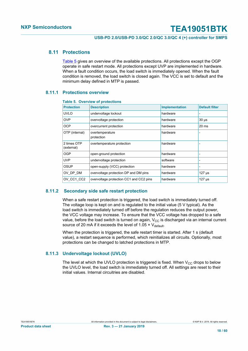
8.11 Protections
Table 5 gives an overview of the available protections. All protections except the OGPoperate in safe restart mode. All protections except UVP are implemented in hardware.When a fault condition occurs, the load switch is immediately opened. When the faultcondition is removed, the load switch is closed again. The VCC is set to default and theminimum delay defined in MTP is passed.
8.11.1 Protections overview
Table 5. Overview of protectionsProtection Description Implementation Default filter
UVLO undervoltage lockout hardware -
OVP overvoltage protection hardware 30 μs
OCP overcurrent protection hardware 20 ms
OTP (internal) overtemperatureprotection
hardware -
2 times OTP(external)
overtemperature protection hardware -
OGP open-ground protection hardware -
UVP undervoltage protection software -
OSUP open-supply (VCC) protection hardware -
OV_DP_DM overvoltage protection DP and DM pins hardware 127 μs
OV_CC1_CC2 overvoltage protection CC1 and CC2 pins hardware 127 μs
8.11.2 Secondary side safe restart protection
When a safe restart protection is triggered, the load switch is immediately turned off.The voltage loop is kept on and is regulated to the initial value (5 V typical). As theload switch is immediately turned off before the regulation reduces the output power,the VCC voltage may increase. To ensure that the VCC voltage has dropped to a safevalue, before the load switch is turned on again, VCC is discharged via an internal currentsource of 20 mA if it exceeds the level of 1.05 × Vdefault.
When the protection is triggered, the safe restart timer is started. After 1 s (defaultvalue), a restart sequence is performed, which reinitializes all circuits. Optionally, mostprotections can be changed to latched protections in MTP.
8.11.3 Undervoltage lockout (UVLO)
The level at which the UVLO protection is triggered is fixed. When VCC drops to belowthe UVLO level, the load switch is immediately turned off. All settings are reset to theirinitial values. Internal circuitries are disabled.

NXP Semiconductors TEA19051BTKUSB-PD 2.0/USB-PD 3.0/QC 2.0/QC 3.0/QC 4 (+) controller for SMPS
TEA19051BTK All information provided in this document is subject to legal disclaimers. © NXP B.V. 2019. All rights reserved.
Product data sheet Rev. 3 — 21 January 201919 / 60
8.11.4 Overvoltage protection (OVP)
The OVP level is set as a percentage of the requested output voltage level. The OVPlevel is set to default 125 % (V < 9 V) or 120 % (V ≥ 9 V) of the programmed outputvoltage. When VCC continuously exceeds this level for longer than the minimum OVPtime (default 30 μs), the OVP protection is triggered.
8.11.5 Overcurrent protection (OCP)
The default TEA19051BTK setting is CC mode. In CC mode, the current loop definesthe maximum current. Instead, the OCP mode can be selected via MTP. The OCP levelcan be programmed individually for each PDO. OCP is only triggered if the OCP modeis set for the corresponding PDO and the output current is continuously higher than theprogrammed current level for more than the programmed OCP blanking time.
8.11.6 Overtemperature protection (OTP)
8.11.6.1 Internal OTP
When the internally measured temperature exceeds the programmed OTP setting, OTPis triggered, unless the protection is disabled in MTP. The temperature level can bedefined in MTP. The default value is 113 °C.
Furthermore, the internal temperature sensor can be used to measure the temperature.The measured temperature can be sent via USB-PD.
8.11.6.2 External OTP
When the mode "NTC+OTP" is selected for GPIO1 (cable connector temperature) orGPIO2 (adapter temperature) in the MTP and the externally measured temperatureexceeds the programmed OTP setting, OTP is triggered. The temperature level can bedefined in MTP. The default value is 90 °C (see Section 15 and Table 4).
8.11.7 Open-ground protection (OGP)
An open-ground event is detected by monitoring the difference in voltage betweenthe GND and SGND pins. When the difference is greater than the specified maximumvoltage difference, OGP is triggered, unless the protection is disabled.
This feature protects the application from supplying high currents to the load when theground pins of the sense resistor are not properly connected.
8.11.8 Open-supply protection (OSUP)
When the IC is not supplied via the VCC pin any more, the voltage on the OPTO pin isused to open the external load switch. Opening the external load switch prevents that theload is damaged if the VCC pin is disconnected.
8.11.9 Undervoltage protection (UVP)
The UVP level is set to 60 % PDO level. The reaction to a triggering of UVP isprogrammed in the firmware. The protection is a safe restart protection by default. Thelevel can never be lower than the UVLO level. The level can be adjusted via MTP.

NXP Semiconductors TEA19051BTKUSB-PD 2.0/USB-PD 3.0/QC 2.0/QC 3.0/QC 4 (+) controller for SMPS
TEA19051BTK All information provided in this document is subject to legal disclaimers. © NXP B.V. 2019. All rights reserved.
Product data sheet Rev. 3 — 21 January 201920 / 60
8.11.10 Output short protection (OSP)
At a shorted output, the VCC voltage drops to below the UVLO level. The load switchis turned off. After the programmed safe restart time, the output is enabled again. Tomeet the average input power requirement at a shorted output, a proper safe restart timemust be chosen. When the VCC voltage exceeds the UVLO level, the primary controllerinitially limits the maximum output power.
Because the safe restart time is set to 1 s, the dissipation is limited to < 50 mW. Thislimitation prevents that the application heats up when the output is shorted.
8.11.11 OVP DP and DM pins (OV_DP_DM)
The overvoltage protection of the DP and DM pins can be enabled in MTP. However, it isswitched off by default.
OV_DP_DM is a safe restart protection. When the DP or DM pin is shorted to Vbus,this protection is triggered. The trigger level of the OV_DP_DM is at 4.5 V. To preventunwanted triggering, it has a 127 µs (default) blanking time.
8.11.12 OVP CC1 and CC2 pins (OV_CC1_CC2)
The overvoltage protection of the CC1 and CC2 pins can be enabled in MTP. However, itis switched off by default.
OV_CC1_CC2 is a safe restart protection. When the CC1 or CC2 pin is shorted to Vbus,this protection is triggered. The trigger level of the OV_CC1_CC2 is at 4.5 V. To preventunwanted triggering, it has a 127 µs (default) blanking time.
8.11.13 Soft short protection CC pins (SHORT_CC1_CC2)
The CC pins are protected with a soft-short protection that measures the impedanceof the CC lines. When the measured impedance is not according to the USB-PDspecification, the load switch is opened.

NXP Semiconductors TEA19051BTKUSB-PD 2.0/USB-PD 3.0/QC 2.0/QC 3.0/QC 4 (+) controller for SMPS
TEA19051BTK All information provided in this document is subject to legal disclaimers. © NXP B.V. 2019. All rights reserved.
Product data sheet Rev. 3 — 21 January 201921 / 60
9 Limiting valuesTable 6. Limiting valuesIn accordance with the Absolute Maximum Rating System (IEC 60134).
Symbol Parameter Conditions Min Max Unit
Voltages
VVCC voltage on pin VCC −0.5 +26 V
VOPTO voltage on pin OPTO −0.5 +26 V
VCC1 voltage on pin CC1 −0.5 +26 V
VCC2 voltage on pin CC2 −0.5 +26 V
VDP voltage on pin DP −0.5 +6 V
VDM voltage on pin DM −0.5 +6 V
VSW voltage on pin SW −0.5 VCC + 9 V
VDISCH voltage on pin DISCH −0.5 +26 V
VVSNS voltage on pin VSNS −0.5 +3.6 V
VISNS voltage on pin ISNS −0.5 +3.6 V
VGPIO1 voltage on pin GPIO1 −0.5 +3.6 V
VGPIO2 voltage on pin GPIO2 −0.5 +3.6 V
VSDA voltage on pin SDA −0.5 +3.6 V
VSCL voltage on pin SCL −0.5 +3.6 V
General
Tstg storage temperature −65 +150 °C
Tj junction temperature −40 +150 °C
Electrosatic discharge (ESD)
human body model(HBM)
−2000 +2000 V
charged device model(CDM)
−500 +500 V
VESD electrostatic dischargevoltage
machine model (MM) −200 +200 V

NXP Semiconductors TEA19051BTKUSB-PD 2.0/USB-PD 3.0/QC 2.0/QC 3.0/QC 4 (+) controller for SMPS
TEA19051BTK All information provided in this document is subject to legal disclaimers. © NXP B.V. 2019. All rights reserved.
Product data sheet Rev. 3 — 21 January 201922 / 60
10 Recommended operating conditionsTable 7. Recommended operating conditionsSymbol Parameter Conditions Min Max Unit
Voltages
VVCC voltage on pin VCC 0 21 V
VOPTO voltage on pin OPTO 0 21 V
VCC1 voltage on pin CC1 0 5 V
VCC2 voltage on pin CC2 0 5 V
VDP voltage on pin DP 0 5 V
VDM voltage on pin DM 0 5 V
VSW voltage on pin SW 0 VCC + 6 V
VDISCH voltage on pin DISCH 0 21 V
VVSNS voltage on pin VSNS 0 2.5 V
VISNS voltage on pin ISNS 0 3.3 V
VGPIO1 voltage on pin GPIO1 0 3.3 V
VGPIO2 voltage on pin GPIO2 0 3.3 V
VSDA voltage on pin SDA 0 3.3 V
VSCL voltage on pin SCL 0 3.3 V
General
Tj junction temperature −20 +105 °C
11 Thermal characteristicsTable 8. Thermal characteristicsSymbol Parameter Conditions Typ Unit
Rth(j-a) thermal resistance fromjunction to ambient
JEDEC test board 60 K/W
Rth(j-c) thermal resistance fromjunction to case
JEDEC test board 30 K/W

NXP Semiconductors TEA19051BTKUSB-PD 2.0/USB-PD 3.0/QC 2.0/QC 3.0/QC 4 (+) controller for SMPS
TEA19051BTK All information provided in this document is subject to legal disclaimers. © NXP B.V. 2019. All rights reserved.
Product data sheet Rev. 3 — 21 January 201923 / 60
12 CharacteristicsTable 9. CharacteristicsTamb = 25 °C; VCC = 5.0 V; all voltages are measured with respect to GND; currents are positive when flowing into the IC;unless otherwise specified.
Symbol Parameter Conditions Min Typ Max Unit
Supply (VCC pin)
Vth(UVLO) undervoltage lockoutthreshold
falling - 2.85 2.9 V
unattached; VCC = 5 V - 1.8 - mAICC supply current
nominal; VCC = 5 V - 3 - mA
extra discharge current;VCC = 1.05 × Vo(default)
- 20 - mAICC(dch) discharge supplycurrent
discharge current ofVCC during safe restartprotection; depends onload conditions
- 20 - mA
Vos overshoot voltage protection level voltage - 1.05 × Vo(default) - V
CC1/CC2 section (CC1 and CC2 pins)
Type C
current source for DFP pull-up indication
default current −96 −80 −64 μA
1.5 A mode −194 −180 −166 μA
Ipu pull-up current
3 A mode −356 −330 −304 μA
with standard 5.1 kΩ pull-down resistance
default current 1.5 1.6 1.7 V
1.5 A mode 1.5 1.6 1.7 V
VIH HIGH-level inputvoltage
3 A mode 2.45 2.60 2.75 V
with standard 5.1 kΩ pull-down resistance
default current 0.15 0.2 0.25 V
1.5 A mode 0.35 0.40 0.45 V
VIL LOW-level input voltage
3 A mode 0.75 0.80 0.85 V
Vovp overvoltage protectionvoltage
CC1 and CC2 pins - 4.5 - V
USB-PD normative specification
fbit bit rate BMC bit rate 270 300 330 Kbps
NXP Semiconductors TEA19051BTKUSB-PD 2.0/USB-PD 3.0/QC 2.0/QC 3.0/QC 4 (+) controller for SMPS
TEA19051BTK All information provided in this document is subject to legal disclaimers. © NXP B.V. 2019. All rights reserved.
Product data sheet Rev. 3 — 21 January 201924 / 60
Symbol Parameter Conditions Min Typ Max Unit
USB-PD transmitter normative specification
tfall fall time 10 % and 90% amplitudepoints; minimum isunderloaded condition
300 - 650 ns
trise rise time 10 % and 90% amplitudepoints; minimum isunderloaded condition
300 - 650 ns
Vo output voltage signal voltage swing 1.05 1.125 1.2 V
Zo output impedance transmitter - 45 - Ω
USB-PD receiver normative specification
Cin input capacitance receiver - 250 - pF
|tfltr(lim) time constant limitingfilter
receiver bandwidth 100 - - ns
zi input impedance receiver 10 - - MΩ
receiver comparator
low level - 0.55 - V
high level - 0.8 - V
Vi input voltage
hysteresis - 250 - mV
DP and DM pins
Vovp overvoltage protectionvoltage
DM and DP pins - 4.5 - V
Qualcomm® QuickCharge™ QC2.0 and QC3.0
Rsw switch resistance when DP and DM pinsare shorted
- - 20 Ω
DM and DP comparator pins
high level 1.8 2.0 2.2 V
Vi input voltage
low level 0.250 0.325 0.400 V
pin DP 300 900 1500 kΩRpd pull-down resistance
pin DM 14.25 19.53 24.80 kΩ
attach debounce time(BC1.2)
1 - 1.5 s
DM low debouncetime after BC1.2 iscompleted
1 - - ms
td delay time
signal detectiondebounce time
20 40 60 ms

NXP Semiconductors TEA19051BTKUSB-PD 2.0/USB-PD 3.0/QC 2.0/QC 3.0/QC 4 (+) controller for SMPS
TEA19051BTK All information provided in this document is subject to legal disclaimers. © NXP B.V. 2019. All rights reserved.
Product data sheet Rev. 3 — 21 January 201925 / 60
Symbol Parameter Conditions Min Typ Max Unit
Voltage control (VSNS pin)
Vref reference voltage input voltage range onthe VSNS pin to controlthe voltage loop
0.3 - 2.4 V
voltage loop accuracy;VCC = 5 V
−2 - +2 %Vacc voltage accuracy
measurement voltageaccuracy
−2 - +2 %
gm transconductance VCC in; OPTO out 4 - - mA/mV
Gmax maximum gain cable compensation - 8 - mV/mV
Current control (ISNS pin)
Iref reference current parameter can beprogrammed in MTP 10bits
0 - 40 mV
current loop accuracy; Rsense = 5 mΩ
0.5 A < Iout < 5 A −100 - +100 mA
Iout > 5 A −2 - +2 %
measurement current accuracy; Rsense = 5 mΩ
0.5 A < Iout < 5 A [1] −100 - +100 mA
Iout output current
Iout > 5 A −3 - +3 %
gain current;amplifier = 50
200 - mA/mVgm transconductance
gain current;amplifier = 25
100 - - mA/mV
GPIO1 and GPIO2 pins
GPIO function = NTC (+OTP)
low temperatures(see Figure 6)
−15.75 −15.00 −14.25 μA
mediumtemperatures(see Figure 6)
−63 −60 −57 μA
IO(GPIOX) output current on pinGPIOX
high temperatures(see Figure 6)
−252 −240 −228 μA
Tacc temperature accuracy 47 kΩ NTC(Beta = 4108)
−5 - +5 °C
Tres temperature resolution temperaturemeasurement
−1 - +1 °C
high level 1.5 - - VVI input voltage
low level - - 0.9 V
GPIO function = supply
high level; no load 2.7 3.0 3.3 V
VO output voltage
low level; no load - - 0.3 V

NXP Semiconductors TEA19051BTKUSB-PD 2.0/USB-PD 3.0/QC 2.0/QC 3.0/QC 4 (+) controller for SMPS
TEA19051BTK All information provided in this document is subject to legal disclaimers. © NXP B.V. 2019. All rights reserved.
Product data sheet Rev. 3 — 21 January 201926 / 60
Symbol Parameter Conditions Min Typ Max Unit
GPIO function = supply
source; VO = 2.3 V - - −1 mA
IO output current
sink; VO = 0.4 V 1 - - mA
SDA and SCL pins
high level 2.1 - - VVI input voltage
low level - - 0.9 V
IO output current Vo(SCL/SDA) = 0.6 V 6 - - mA
Vpu pull-up voltage - 3 - V
Rpu pull-up resistance for SDA and SCL - 1 - kΩ
Protections
Vovp overvoltage protectionvoltage
with control loop involtage control mode
3 - 25 V
Vovp(acc) overvoltage protectionvoltage accuracy
VCC pin; Vovp = 6 V −3 - +3 %
Vocp overcurrent protectionvoltage
6 - 40 mV
Vocp(acc) overcurrent protectionvoltage accuracy
−3 - +3 %
Vuvp undervoltage protectionvoltage
3 - 21 V
Vuvp(acc) undervoltage protectionvoltage accuracy
−3 - +3 %
ICC(dch) discharge supplycurrent
during safe restartprotection
- 20 - mA
SW driver
switch-on - 80 - kΩRO output resistance
switch-off - 600 - Ω
DISCH part (DISCH pin)
Rdch discharge resistance - 3 - Ω
Vdet(rst) reset detection voltage hard reset 0.65 0.70 0.75 V
tact active time maximum on-timeduring attached state
- 100 - ms
OPTO pin
IO(min) minimum output current - 30 - μA
IO(max) maximum outputcurrent
3.75 5 6.25 mA
Internal oscillator
fosc internal oscillatorfrequency
- 10 - MHz

NXP Semiconductors TEA19051BTKUSB-PD 2.0/USB-PD 3.0/QC 2.0/QC 3.0/QC 4 (+) controller for SMPS
TEA19051BTK All information provided in this document is subject to legal disclaimers. © NXP B.V. 2019. All rights reserved.
Product data sheet Rev. 3 — 21 January 201927 / 60
Symbol Parameter Conditions Min Typ Max Unit
Internal temperature protection
Totp(acc) overtemperatureprotection trip accuracy
temperatureregarding the trip levelprogrammed in MTP
−10 - +10 °C
[1] The current sense pin can be used up to 40 mV. The result is a current range that depends on the programmed Rsense resistor. (e.g. with 10 mΩ, the valuecan be up to 4 A).

NXP Semiconductors TEA19051BTKUSB-PD 2.0/USB-PD 3.0/QC 2.0/QC 3.0/QC 4 (+) controller for SMPS
TEA19051BTK All information provided in this document is subject to legal disclaimers. © NXP B.V. 2019. All rights reserved.
Product data sheet Rev. 3 — 21 January 201928 / 60
13 Application information
aaa-025897
TEA193x
HV DRIVERS1
R2
R3
R1
R7
R4
C1
NTC1(near connector)
NTC2(adapter)
R5
ISENSE
AUX
VCCH
VCCL
CTRL
GND
PROTECT
n.c.
TEA19051B
VCC SW
VbusVCC
GND
DISCH
DP
DM
SDA
SGND
GPIO1
ISNS
CC1
CC2
GPIO2
VSNS
SCL
EDP
OPTO
TEA199x
DRAIN
CAP
XV
GND
SOURCE
GATE
C2
R6
Figure 7. Typical application diagram, including TEA1938, TEA1999 (low-side SR), and TEA19051BTK
13.1 Resistor divider
The resistor divider (R3 / (R2 + R3) connected from the VCC pin to the VSNS pin mustreduce the output voltage to < 2.5 V for the maximum output voltage. See Section 8.2 formore information about the divider ratios. To minimize the voltage drop at the connector,the resistor divider must be connected as close as possible to the load switch.
It is important that the external resistive divider exactly matches the internal value (MTP),because internal measurements depend on it. In the resistive divider, use resistors with a1 % or better accuracy.

NXP Semiconductors TEA19051BTKUSB-PD 2.0/USB-PD 3.0/QC 2.0/QC 3.0/QC 4 (+) controller for SMPS
TEA19051BTK All information provided in this document is subject to legal disclaimers. © NXP B.V. 2019. All rights reserved.
Product data sheet Rev. 3 — 21 January 201929 / 60
13.2 Sense resistor
The accuracy of the sense resistor R1 is very important. Any deviation from the value inMTP gives an offset in the current measurement. Because the sense resistor is very low-ohmic, the layout of the connections in the PCB can give major deviations from its initialvalue.
To overcome these deviations, several options are available:
• Change the sense resistor value such that the complete value is matching the typicalMTP value (5 mΩ or 10 mΩ).
• Trim the value with a resistor divider so that the (R7 / (R5 + R7)) × (R1 + RPCB)matches the MTP default value. RPCB is the resistance of copper wires and theresistance change of the sense resistor due to its soldering profile.
To maximize accuracy and temperature stability, keep Rpcb as low as possible. Thesense resistor must have a temperature coefficient that is as low as possible. To preventmagnetic coupling, keep the length and the area of the connections between the senseresistor and the SGND and ISNS pins as small as possible.
Connect the exposed die pad to the GND pin. Ensure that high currents flowing throughthe plane below the IC is prevented.
13.3 Voltage loop
In the application diagram, an integrator network is connected between the VSNS pinand the optocoupler. The recommended values of these components are:
• R2 = 160 kΩ to 180 kΩ• R4 = 1 kΩ• C1 = 10 nF; for the integral part
To prevent magnetic coupling to these parts, which results in pollution in output voltage,the length and the area of the connection must be kept as small as possible.
13.4 Current loop
For applications using the CC loop in the application, an integrator network is connectedbetween the ISNS pin and the optocoupler. The recommended values for thesecomponents are:
• R5 = 330 Ω when R1 = 10 mΩ; R5 = 160 Ω when R1 = 5 mΩ; connected betweensense resistor and the ISNS pin for the proportional part.
• R6 = 5 kΩ• C2 = 100 nF; for the integral part
To prevent magnetic coupling to these parts, which results in pollution in output currents,the length and the area of the connection must be kept as small as possible.
Resistor R6 and capacitor C2 can be removed in applications that use OCP mode.
NXP Semiconductors TEA19051BTKUSB-PD 2.0/USB-PD 3.0/QC 2.0/QC 3.0/QC 4 (+) controller for SMPS
TEA19051BTK All information provided in this document is subject to legal disclaimers. © NXP B.V. 2019. All rights reserved.
Product data sheet Rev. 3 — 21 January 201930 / 60
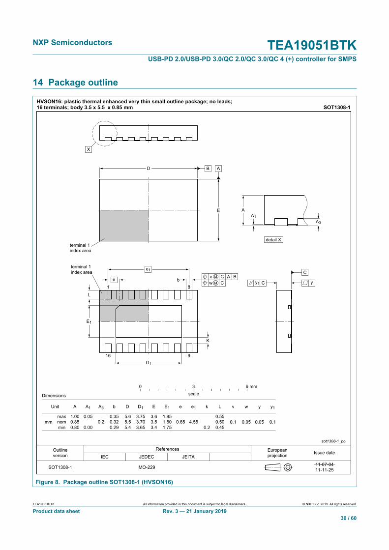
14 Package outline
b
e1
e AC BvCw
1 8
terminal 1index area
K
D1
L
E1
16 9
ReferencesOutlineversion
Europeanprojection Issue date
IEC JEDEC JEITA
SOT1308-1 MO-229
sot1308-1_po
11-07-0411-11-25
Unit
mmmaxnommin
1.000.850.80
0.05
0.00
A
Dimensions
HVSON16: plastic thermal enhanced very thin small outline package; no leads;16 terminals; body 3.5 x 5.5 x 0.85 mm SOT1308-1
A1
X
terminal 1index area
0.23.753.703.65
5.65.55.4
3.63.53.4 0.2
A3 b
0.350.320.29
D D1 E E1
1.851.801.75
e e1
4.550.65
k
0.550.500.45
0.1
L v
0.1
w
0.05
y
0.05
y1
0 3 6 mmscale
B AD
E
detail X
A3
AA1
C
yCy1
Figure 8. Package outline SOT1308-1 (HVSON16)

NXP Semiconductors TEA19051BTKUSB-PD 2.0/USB-PD 3.0/QC 2.0/QC 3.0/QC 4 (+) controller for SMPS
TEA19051BTK All information provided in this document is subject to legal disclaimers. © NXP B.V. 2019. All rights reserved.
Product data sheet Rev. 3 — 21 January 201931 / 60
15 Appendix: Internal parameter settings per type
In this section, the internal parameter settings per type are given.
15.1 TEA19051BAATK
Table 10 gives an overview of the function settings in the TEA19051BAATK.
Table 10. Internal parameter settingsFunction TEA19051BAATK
power rating 27 W
supported standards USB-PD3[1]; QC4+
default output voltage 5 V
default maximum output current 3 A
GPIO1 function NTC with OTP
GPIO1 protection level 90 °C
GPIO2 function NTC with OTP
GPIO2 protection level 90 °C
chip OTP trigger level 113 °C
external sense resistor (Rsense) 10 mΩ
external resistor divider VCC/VSNS (= DIV) 5.476
cable compensation 117 mV/A
CC mode or OCP CC mode
OCP level/CC mode margin 5 %
PDO1
PPS enable FALSE
voltage 5 V
current 3 A
OVP level 125 %
UVP level off
QC enable TRUE
cable compensation enable TRUE
PDO2
PPS enable FALSE
voltage 9 V
current 3 A
OVP level 120 %
UVP level 60 %
QC enable TRUE
cable compensation enable TRUE

NXP Semiconductors TEA19051BTKUSB-PD 2.0/USB-PD 3.0/QC 2.0/QC 3.0/QC 4 (+) controller for SMPS
TEA19051BTK All information provided in this document is subject to legal disclaimers. © NXP B.V. 2019. All rights reserved.
Product data sheet Rev. 3 — 21 January 201932 / 60
Function TEA19051BAATK
PDO3
PPS enable FALSE
voltage 12 V
current 2.25 A
OVP level 120 %
UVP level 60 %
QC enable TRUE
cable compensation enable TRUE
PDO4
PPS enable TRUE
maximum voltage 5.9 V
minimum voltage 3.3 V
maximum current 3 A
power limit enabled FALSE
OVP level 125 %
UVP level 90 %
QC enable FALSE
cable compensation enable FALSE
PDO5
PPS enable TRUE
maximum voltage 11 V
minimum voltage 3.3 V
maximum current 3 A
power limit enabled TRUE
OVP level 120 %
UVP level 90 %
QC enable FALSE
cable compensation enable FALSE
[1] To make USB-PD3 certification possible, the DP and DM pins of the IC must not be connected. To pass BC1.2, the DPand DM pins of the connector must be connected to each other.

NXP Semiconductors TEA19051BTKUSB-PD 2.0/USB-PD 3.0/QC 2.0/QC 3.0/QC 4 (+) controller for SMPS
TEA19051BTK All information provided in this document is subject to legal disclaimers. © NXP B.V. 2019. All rights reserved.
Product data sheet Rev. 3 — 21 January 201933 / 60
15.2 TEA19051BABTK
Table 11 gives an overview of the function settings in the TEA19051BABTK.
Table 11. Internal parameter settingsFunction TEA19051BABTK
power rating 45 W
supported standards USB-PD3[1];QC2.0; QC3.0
default output voltage 5 V
default maximum output current 3 A
GPIO1 function NTC with OTP
GPIO1 protection level 90 °C
GPIO2 function NTC with OTP
GPIO2 protection level 90 °C
chip OTP trigger level 113 °C
external sense resistor (Rsense) 10 mΩ
external resistor divider VCC/VSNS (= DIV) 8.325
cable compensation 100 mV/A
CC mode or OCP OCP
OCP level/CC mode margin 5 %
PDO1
PPS enable FALSE
voltage 5 V
current 3 A
OVP level 125 %
UVP level off
QC enable TRUE
cable compensation enable TRUE
PDO2
PPS enable FALSE
voltage 9 V
current 3 A
OVP level 120 %
UVP level 60 %
QC enable TRUE
cable compensation enable TRUE

NXP Semiconductors TEA19051BTKUSB-PD 2.0/USB-PD 3.0/QC 2.0/QC 3.0/QC 4 (+) controller for SMPS
TEA19051BTK All information provided in this document is subject to legal disclaimers. © NXP B.V. 2019. All rights reserved.
Product data sheet Rev. 3 — 21 January 201934 / 60
Function TEA19051BABTK
PDO3
PPS enable FALSE
voltage 12 V
current 3 A
OVP level 120 %
UVP level 60 %
QC enable TRUE
cable compensation enable TRUE
PDO4
PPS enable FALSE
voltage 15 V
current 3 A
OVP level 120 %
UVP level 60 %
QC enable FALSE
cable compensation enable TRUE
PDO5
PPS enable FALSE
voltage 20 V
current 2.25 A
OVP level 120 %
UVP level 60 %
QC enable FALSE
cable compensation enable TRUE
[1] To make USB-PD3 certification possible, the DP and DM pins of the IC must not be connected. To pass BC1.2, the DPand DM pins of the connector must be connected to each other.
NXP Semiconductors TEA19051BTKUSB-PD 2.0/USB-PD 3.0/QC 2.0/QC 3.0/QC 4 (+) controller for SMPS
TEA19051BTK All information provided in this document is subject to legal disclaimers. © NXP B.V. 2019. All rights reserved.
Product data sheet Rev. 3 — 21 January 201935 / 60
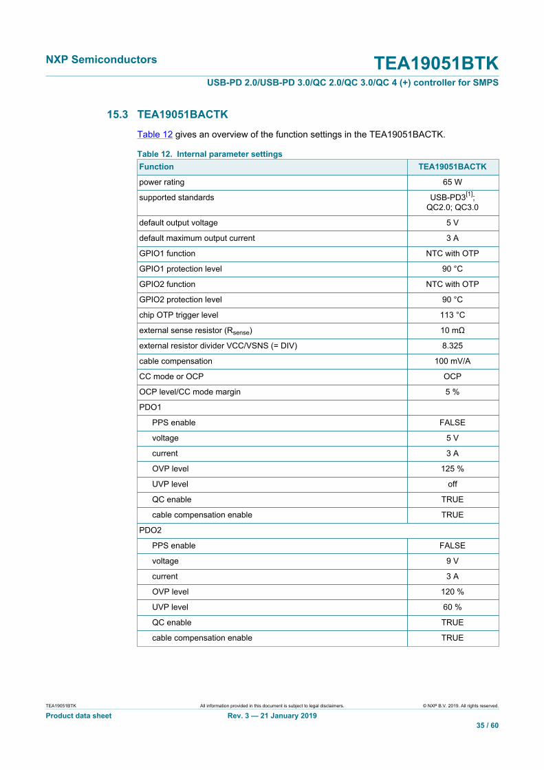
15.3 TEA19051BACTK
Table 12 gives an overview of the function settings in the TEA19051BACTK.
Table 12. Internal parameter settingsFunction TEA19051BACTK
power rating 65 W
supported standards USB-PD3[1];QC2.0; QC3.0
default output voltage 5 V
default maximum output current 3 A
GPIO1 function NTC with OTP
GPIO1 protection level 90 °C
GPIO2 function NTC with OTP
GPIO2 protection level 90 °C
chip OTP trigger level 113 °C
external sense resistor (Rsense) 10 mΩ
external resistor divider VCC/VSNS (= DIV) 8.325
cable compensation 100 mV/A
CC mode or OCP OCP
OCP level/CC mode margin 5 %
PDO1
PPS enable FALSE
voltage 5 V
current 3 A
OVP level 125 %
UVP level off
QC enable TRUE
cable compensation enable TRUE
PDO2
PPS enable FALSE
voltage 9 V
current 3 A
OVP level 120 %
UVP level 60 %
QC enable TRUE
cable compensation enable TRUE

NXP Semiconductors TEA19051BTKUSB-PD 2.0/USB-PD 3.0/QC 2.0/QC 3.0/QC 4 (+) controller for SMPS
TEA19051BTK All information provided in this document is subject to legal disclaimers. © NXP B.V. 2019. All rights reserved.
Product data sheet Rev. 3 — 21 January 201936 / 60
Function TEA19051BACTK
PDO3
PPS enable FALSE
voltage 12 V
current 3 A
OVP level 120 %
UVP level 60 %
QC enable TRUE
cable compensation enable TRUE
PDO4
PPS enable FALSE
voltage 15 V
current 3 A
OVP level 120 %
UVP level 60 %
QC enable FALSE
cable compensation enable TRUE
PDO5
PPS enable FALSE
voltage 20 V
current 3.25 A
OVP level 120 %
UVP level 60 %
QC enable FALSE
cable compensation enable TRUE
[1] To make USB-PD3 certification possible, the DP and DM pins of the IC must not be connected. To pass BC1.2, the DPand DM pins of the connector must be connected to each other.

NXP Semiconductors TEA19051BTKUSB-PD 2.0/USB-PD 3.0/QC 2.0/QC 3.0/QC 4 (+) controller for SMPS
TEA19051BTK All information provided in this document is subject to legal disclaimers. © NXP B.V. 2019. All rights reserved.
Product data sheet Rev. 3 — 21 January 201937 / 60
15.4 TEA19051BAFTK
Table 13 gives an overview of the function settings in the TEA19051BAFTK.
Table 13. Internal parameter settingsFunction TEA19051BAFTK
power rating 18 W
supported standards USB-PD3[1]; QC4+
default output voltage 5.10 V
default maximum output current 3 A
GPIO1 function NTC with OTP
GPIO1 protection level 90 °C
GPIO2 function disabled
GPIO2 protection level -
chip OTP trigger level 113 °C
external sense resistor (Rsense) 10 mΩ
external resistor divider VCC/VSNS (= DIV) 5.476
cable compensation 88 mV/A
CC mode or OCP CC mode
OCP level/CC mode margin 5 %
PDO1
PPS enable FALSE
voltage 5.10 V
current 3 A
OVP level 125 %
UVP level OFF
QC enable TRUE
cable compensation enable TRUE
PDO2
PPS enable FALSE
voltage 9 V
current 2 A
OVP level 120 %
UVP level 60 %
QC enable TRUE
cable compensation enable TRUE
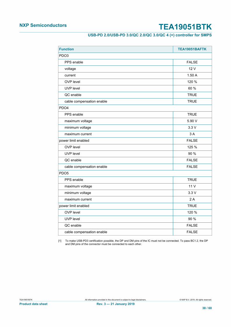
NXP Semiconductors TEA19051BTKUSB-PD 2.0/USB-PD 3.0/QC 2.0/QC 3.0/QC 4 (+) controller for SMPS
TEA19051BTK All information provided in this document is subject to legal disclaimers. © NXP B.V. 2019. All rights reserved.
Product data sheet Rev. 3 — 21 January 201938 / 60
Function TEA19051BAFTK
PDO3
PPS enable FALSE
voltage 12 V
current 1.50 A
OVP level 120 %
UVP level 60 %
QC enable TRUE
cable compensation enable TRUE
PDO4
PPS enable TRUE
maximum voltage 5.90 V
minimum voltage 3.3 V
maximum current 3 A
power limit enabled FALSE
OVP level 125 %
UVP level 90 %
QC enable FALSE
cable compensation enable FALSE
PDO5
PPS enable TRUE
maximum voltage 11 V
minimum voltage 3.3 V
maximum current 2 A
power limit enabled TRUE
OVP level 120 %
UVP level 90 %
QC enable FALSE
cable compensation enable FALSE
[1] To make USB-PD3 certification possible, the DP and DM pins of the IC must not be connected. To pass BC1.2, the DPand DM pins of the connector must be connected to each other.

NXP Semiconductors TEA19051BTKUSB-PD 2.0/USB-PD 3.0/QC 2.0/QC 3.0/QC 4 (+) controller for SMPS
TEA19051BTK All information provided in this document is subject to legal disclaimers. © NXP B.V. 2019. All rights reserved.
Product data sheet Rev. 3 — 21 January 201939 / 60
15.5 TEA19051BAGTK
Table 14 gives an overview of the function settings in the TEA19051BAGTK.
Table 14. Internal parameter settingsFunction TEA19051BAGTK
power rating 27 W
supported standards USB-PD3[1]; QC4+
default output voltage 5 V
default maximum current 3 A
GPIO1 function NTC with OTP
GPIO1 protection level 90 °C
GPIO2 function disabled
GPIO2 protection level -
chip OTP trigger level 113 °C
external sense resistor (Rsense) 10 mΩ
external resistor divider VCC/VSNS (= DIV) 8.325
cable compensation 111 mV/A
CC mode or OCP CC mode
OCP level/CC mode margin 5 %
PDO1
PPS enable FALSE
voltage 5 V
current 3 A
OVP level 125 %
UVP level OFF
QC enable TRUE
cable compensation enable TRUE
PDO2
PPS enable FALSE
voltage 9 V
current 3 A
OVP level 120 %
UVP level 60 %
QC enable TRUE
cable compensation enable TRUE

NXP Semiconductors TEA19051BTKUSB-PD 2.0/USB-PD 3.0/QC 2.0/QC 3.0/QC 4 (+) controller for SMPS
TEA19051BTK All information provided in this document is subject to legal disclaimers. © NXP B.V. 2019. All rights reserved.
Product data sheet Rev. 3 — 21 January 201940 / 60
Function TEA19051BAGTK
PDO3
PPS enable FALSE
voltage 12 V
current 2.25 A
OVP level 120 %
UVP level 60 %
QC enable TRUE
cable compensation enable TRUE
PDO4
PPS enable FALSE
voltage 15 V
current 1.80 A
OVP level 120 %
UVP level 60 %
QC enable FALSE
cable compensation enable TRUE
PDO5
PPS enable FALSE
voltage 20 V
current 1.35 A
OVP level 120 %
UVP level 60 %
QC enable FALSE
cable compensation enable TRUE
PDO6
PPS enable TRUE
maximum voltage 11 V
minimum voltage 3.3 V
maximum current 3 A
power limit enabled TRUE
OVP level 120 %
UVP level 90 %
QC enable FALSE
cable compensation enable FALSE
[1] To make USB-PD3 certification possible, the DP and DM pins of the IC must not be connected. To pass BC1.2, the DPand DM pins of the connector must be connected to each other.

NXP Semiconductors TEA19051BTKUSB-PD 2.0/USB-PD 3.0/QC 2.0/QC 3.0/QC 4 (+) controller for SMPS
TEA19051BTK All information provided in this document is subject to legal disclaimers. © NXP B.V. 2019. All rights reserved.
Product data sheet Rev. 3 — 21 January 201941 / 60
15.6 TEA19051BAHTK
Table 15 gives an overview of the function settings in the TEA19051BAHTK.
Table 15. Internal parameter settingsFunction TEA19051BAHTK
power rating 30 W
supported standards QC2; QC3[1]
default output voltage 5 V
default maximum current 3 A
GPIO1 function NTC with OTP
GPIO1 protection level 90 °C
GPIO2 function disabled
GPIO2 protection level -
chip OTP trigger level 113 °C
external sense resistor (Rsense) 10 mΩ
external resistor divider VCC/VSNS (= DIV) 5.476
cable compensation 117 mV/A
CC mode or OCP CC mode
OCP level/CC mode margin 5 %
PDO1
PPS enable FALSE
voltage 5 V
current 3 A
OVP level 125 %
UVP level OFF
QC enable TRUE
cable compensation enable TRUE
PDO2
PPS enable FALSE
voltage 6 V
current 3 A
OVP level 125 %
UVP level 60 %
QC enable FALSE
cable compensation enable TRUE
NXP Semiconductors TEA19051BTKUSB-PD 2.0/USB-PD 3.0/QC 2.0/QC 3.0/QC 4 (+) controller for SMPS
TEA19051BTK All information provided in this document is subject to legal disclaimers. © NXP B.V. 2019. All rights reserved.
Product data sheet Rev. 3 — 21 January 201942 / 60
Function TEA19051BAHTK
PDO3
PPS enable FALSE
voltage 9 V
current 3 A
OVP level 120 %
UVP level 60 %
QC enable TRUE
cable compensation enable TRUE
PDO4
PPS enable FALSE
voltage 12 V
maximum current 2.5 A
OVP level 120 %
UVP level 60 %
QC enable TRUE
cable compensation enable TRUE
PDO5
PPS enable TRUE
maximum voltage 5.9 V
minimum voltage 3.3 V
maximum current 3 A
power limit enabled FALSE
OVP level 125 %
UVP level 90 %
QC enable FALSE
cable compensation enable FALSE
PDO6
PPS enable TRUE
maximum voltage 11 V
minimum voltage 3.3 V
maximum current 3 A
power limit enabled TRUE
OVP level 125 %
UVP level 90 %
QC enable FALSE
cable compensation enable FALSE
[1] The TEA19051BAH is USB-PD3/QC4 compliant, but USB-PD3/QC4 certification is not possible.
NXP Semiconductors TEA19051BTKUSB-PD 2.0/USB-PD 3.0/QC 2.0/QC 3.0/QC 4 (+) controller for SMPS
TEA19051BTK All information provided in this document is subject to legal disclaimers. © NXP B.V. 2019. All rights reserved.
Product data sheet Rev. 3 — 21 January 201943 / 60
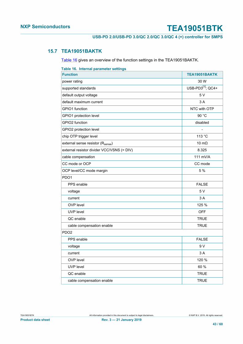
15.7 TEA19051BAKTK
Table 16 gives an overview of the function settings in the TEA19051BAKTK.
Table 16. Internal parameter settingsFunction TEA19051BAKTK
power rating 30 W
supported standards USB-PD3[1]; QC4+
default output voltage 5 V
default maximum current 3 A
GPIO1 function NTC with OTP
GPIO1 protection level 90 °C
GPIO2 function disabled
GPIO2 protection level -
chip OTP trigger level 113 °C
external sense resistor (Rsense) 10 mΩ
external resistor divider VCC/VSNS (= DIV) 8.325
cable compensation 111 mV/A
CC mode or OCP CC mode
OCP level/CC mode margin 5 %
PDO1
PPS enable FALSE
voltage 5 V
current 3 A
OVP level 125 %
UVP level OFF
QC enable TRUE
cable compensation enable TRUE
PDO2
PPS enable FALSE
voltage 9 V
current 3 A
OVP level 120 %
UVP level 60 %
QC enable TRUE
cable compensation enable TRUE
NXP Semiconductors TEA19051BTKUSB-PD 2.0/USB-PD 3.0/QC 2.0/QC 3.0/QC 4 (+) controller for SMPS
TEA19051BTK All information provided in this document is subject to legal disclaimers. © NXP B.V. 2019. All rights reserved.
Product data sheet Rev. 3 — 21 January 201944 / 60
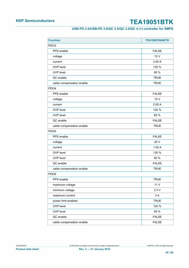
Function TEA19051BAKTK
PDO3
PPS enable FALSE
voltage 12 V
current 2.50 A
OVP level 120 %
UVP level 60 %
QC enable TRUE
cable compensation enable TRUE
PDO4
PPS enable FALSE
voltage 15 V
current 2.00 A
OVP level 120 %
UVP level 60 %
QC enable FALSE
cable compensation enable TRUE
PDO5
PPS enable FALSE
voltage 20 V
current 1.50 A
OVP level 120 %
UVP level 60 %
QC enable FALSE
cable compensation enable TRUE
PDO6
PPS enable TRUE
maximum voltage 11 V
minimum voltage 3.3 V
maximum current 3 A
power limit enabled TRUE
OVP level 120 %
UVP level 90 %
QC enable FALSE
cable compensation enable FALSE

NXP Semiconductors TEA19051BTKUSB-PD 2.0/USB-PD 3.0/QC 2.0/QC 3.0/QC 4 (+) controller for SMPS
TEA19051BTK All information provided in this document is subject to legal disclaimers. © NXP B.V. 2019. All rights reserved.
Product data sheet Rev. 3 — 21 January 201945 / 60
Function TEA19051BAKTK
PDO7
PPS enable TRUE
maximum voltage 16 V
minimum voltage 3.3 V
maximum current 2 A
power limit enabled TRUE
OVP level 120 %
UVP level 90 %
QC enable FALSE
cable compensation enable FALSE
[1] To make USB-PD3 certification possible, the DP and DM pins of the IC must not be connected. To pass BC1.2, the DPand DM pins of the connector must be connected to each other.

NXP Semiconductors TEA19051BTKUSB-PD 2.0/USB-PD 3.0/QC 2.0/QC 3.0/QC 4 (+) controller for SMPS
TEA19051BTK All information provided in this document is subject to legal disclaimers. © NXP B.V. 2019. All rights reserved.
Product data sheet Rev. 3 — 21 January 201946 / 60
15.8 TEA19051BAMTK
Table 17 gives an overview of the function settings in the TEA19051BAMTK.
Table 17. Internal parameter settingsFunction TEA19051BAMTK
power rating 60 W
supported standards USB-PD3[1]; QC4+
default output voltage 5 V
default maximum output current 3 A
GPIO1 function NTC with OTP
GPIO1 protection level 90 °C
GPIO2 function NTC with OTP
GPIO2 protection level 90 °C
chip OTP trigger level 131 °C
external sense resistor (Rsense) 10 mΩ
external resistor divider VCC/VSNS (= DIV) 8.828
cable compensation 118 mV/A
CC mode or OCP CC mode
OCP level/CC mode margin 5 %
PDO1
PPS enable FALSE
voltage 5 V
current 3 A
OVP level 125 %
UVP level OFF
QC enable TRUE
cable compensation enable TRUE
PDO2
PPS enable FALSE
voltage 9 V
current 3 A
OVP level 120 %
UVP level 60 %
QC enable TRUE
cable compensation enable TRUE

NXP Semiconductors TEA19051BTKUSB-PD 2.0/USB-PD 3.0/QC 2.0/QC 3.0/QC 4 (+) controller for SMPS
TEA19051BTK All information provided in this document is subject to legal disclaimers. © NXP B.V. 2019. All rights reserved.
Product data sheet Rev. 3 — 21 January 201947 / 60
Function TEA19051BAMTK
PDO3
PPS enable FALSE
voltage 12 V
current 3.00 A
OVP level 120 %
UVP level 60 %
QC enable TRUE
cable compensation enable TRUE
PDO4
PPS enable FALSE
voltage 15 V
current 3.00 A
OVP level 120 %
UVP level 60 %
QC enable FALSE
cable compensation enable TRUE
PDO5
PPS enable FALSE
voltage 20 V
current 3.00 A
OVP level 120 %
UVP level 60 %
QC enable FALSE
cable compensation enable TRUE
PDO6
PPS enable TRUE
maximum voltage 16 V
minimum voltage 3.3 V
maximum current 3 A
power limit enabled FALSE
OVP level 120 %
UVP level 90 %
QC enable FALSE
cable compensation enable FALSE
NXP Semiconductors TEA19051BTKUSB-PD 2.0/USB-PD 3.0/QC 2.0/QC 3.0/QC 4 (+) controller for SMPS
TEA19051BTK All information provided in this document is subject to legal disclaimers. © NXP B.V. 2019. All rights reserved.
Product data sheet Rev. 3 — 21 January 201948 / 60
Function TEA19051BAMTK
PDO7
PPS enable TRUE
maximum voltage 21 V
minimum voltage 3.3 V
maximum current 3 A
power limit enabled TRUE
OVP level 120 %
UVP level 90 %
QC enable FALSE
cable compensation enable FALSE
[1] To make USB-PD3 certification possible, the DP and DM pins of the IC must not be connected. To pass BC1.2, the DPand DM pins of the connector must be connected to each other.

NXP Semiconductors TEA19051BTKUSB-PD 2.0/USB-PD 3.0/QC 2.0/QC 3.0/QC 4 (+) controller for SMPS
TEA19051BTK All information provided in this document is subject to legal disclaimers. © NXP B.V. 2019. All rights reserved.
Product data sheet Rev. 3 — 21 January 201949 / 60
15.9 TEA19051BAPTK
Table 18 gives an overview of the function settings in the TEA19051BAPTK.
Table 18. Internal parameter settingsFunction TEA19051BAPTK
power rating 27 W
supported standards USB-PD3[1]; QC4+
default output voltage 5 V
default maximum output current 3 A
GPIO1 function NTC with OTP
GPIO1 protection level 90 °C
GPIO2 function disabled
GPIO2 protection level -
chip OTP trigger level 113 °C
external sense resistor (Rsense) 10 mΩ
external resistor divider VCC/VSNS (= DIV) 8.325
cable compensation 111 mV/A
CC mode or OCP CC mode
OCP level/CC mode margin 5 %
PDO1
PPS enable FALSE
voltage 5 V
current 3 A
OVP level 125 %
UVP level OFF
QC enable TRUE
cable compensation enable TRUE
PDO2
PPS enable FALSE
voltage 9 V
current 3 A
OVP level 120 %
UVP level 60 %
QC enable TRUE
cable compensation enable TRUE

NXP Semiconductors TEA19051BTKUSB-PD 2.0/USB-PD 3.0/QC 2.0/QC 3.0/QC 4 (+) controller for SMPS
TEA19051BTK All information provided in this document is subject to legal disclaimers. © NXP B.V. 2019. All rights reserved.
Product data sheet Rev. 3 — 21 January 201950 / 60
Function TEA19051BAPTK
PDO3
PPS enable FALSE
voltage 12 V
current 2.25 A
OVP level 120 %
UVP level 60 %
QC enable TRUE
cable compensation enable TRUE
PDO4
PPS enable FALSE
voltage 15 V
current 1.80 A
OVP level 120 %
UVP level 60 %
QC enable FALSE
cable compensation enable TRUE
PDO5
PPS enable TRUE
maximum voltage 5.90 V
minimum voltage 3.30 V
maximum current 3.00 A
power limit enabled FALSE
OVP level 125 %
UVP level 90 %
QC enable FALSE
cable compensation enable FALSE
PDO6
PPS enable TRUE
maximum voltage 11 V
minimum voltage 3.3 V
maximum current 3 A
power limit enabled TRUE
OVP level 120 %
UVP level
90 %

NXP Semiconductors TEA19051BTKUSB-PD 2.0/USB-PD 3.0/QC 2.0/QC 3.0/QC 4 (+) controller for SMPS
TEA19051BTK All information provided in this document is subject to legal disclaimers. © NXP B.V. 2019. All rights reserved.
Product data sheet Rev. 3 — 21 January 201951 / 60
Function TEA19051BAPTK
QC enable FALSE
cable compensation enable FALSE
[1] To make USB-PD3 certification possible, the DP and DM pins of the IC must not be connected. To pass BC1.2, the DPand DM pins of the connector must be connected to each other.

NXP Semiconductors TEA19051BTKUSB-PD 2.0/USB-PD 3.0/QC 2.0/QC 3.0/QC 4 (+) controller for SMPS
TEA19051BTK All information provided in this document is subject to legal disclaimers. © NXP B.V. 2019. All rights reserved.
Product data sheet Rev. 3 — 21 January 201952 / 60
15.10 TEA19051BARTK
Table 19 gives an overview of the function settings in the TEA19051BARTK.
Table 19. Internal parameter settingsFunction TEA19051BARTK
power rating 100 W
supported standards USB-PD3[1]; QC4+
default output voltage 5 V
default maximum output current 3 A
GPIO1 function NTC with OTP
GPIO1 protection level 90 °C
GPIO2 function NTC with OTP
GPIO2 protection level 90 °C
chip OTP trigger level 113 °C
external sense resistor (Rsense) 5 mΩ
external resistor divider VCC/VSNS (= DIV) 8.828
cable compensation 106 mV/A
CC mode or OCP CC mode
OCP level/CC mode margin 5 %
PDO1
PPS enable FALSE
voltage 5 V
current 3 A
OVP level 125 %
UVP level OFF
QC enable TRUE
cable compensation enable TRUE
PDO2
PPS enable FALSE
voltage 9 V
current 3 A
OVP level 120 %
UVP level 60 %
QC enable TRUE
cable compensation enable TRUE

NXP Semiconductors TEA19051BTKUSB-PD 2.0/USB-PD 3.0/QC 2.0/QC 3.0/QC 4 (+) controller for SMPS
TEA19051BTK All information provided in this document is subject to legal disclaimers. © NXP B.V. 2019. All rights reserved.
Product data sheet Rev. 3 — 21 January 201953 / 60
Function TEA19051BARTK
PDO3
PPS enable FALSE
voltage 12 V
current 3 A
OVP level 120 %
UVP level 60 %
QC enable TRUE
cable compensation enable TRUE
PDO4
PPS enable FALSE
voltage 15 V
current 3 A
OVP level 120 %
UVP level 60 %
QC enable FALSE
cable compensation enable TRUE
PDO5
PPS enable FALSE
voltage 20 V
current 5 A
OVP level 120 %
UVP level 60 %
QC enable FALSE
cable compensation enable TRUE
PDO6
PPS enable TRUE
maximum voltage 16 V
minimum voltage 3.3 V
maximum current 3 A
power limit enabled FALSE
OVP level 120 %
UVP level 90 %
QC enable FALSE
cable compensation enable FALSE

NXP Semiconductors TEA19051BTKUSB-PD 2.0/USB-PD 3.0/QC 2.0/QC 3.0/QC 4 (+) controller for SMPS
TEA19051BTK All information provided in this document is subject to legal disclaimers. © NXP B.V. 2019. All rights reserved.
Product data sheet Rev. 3 — 21 January 201954 / 60
Function TEA19051BARTK
PDO 7
PPS enable TRUE
maximum voltage 21 V
minimum voltage 3.3 V
maximum current 5 A
power limit enabled TRUE
OVP level 120 %
UVP level 90 %
QC enable FALSE
cable compensation enable FALSE
[1] To make USB-PD3 certification possible, the DP and DM pins of the IC must not be connected. To pass BC1.2, the DPand DM pins of the connector must be connected to each other.
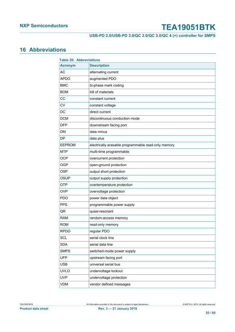
NXP Semiconductors TEA19051BTKUSB-PD 2.0/USB-PD 3.0/QC 2.0/QC 3.0/QC 4 (+) controller for SMPS
TEA19051BTK All information provided in this document is subject to legal disclaimers. © NXP B.V. 2019. All rights reserved.
Product data sheet Rev. 3 — 21 January 201955 / 60
16 AbbreviationsTable 20. AbbreviationsAcronym Description
AC alternating current
APDO augmented PDO
BMC bi-phase mark coding
BOM bill of materials
CC constant current
CV constant voltage
DC direct current
DCM discontinuous conduction mode
DFP downstream facing port
DM data minus
DP data plus
EEPROM electrically erasable programmable read-only memory
MTP multi-time programmable
OCP overcurrent protection
OGP open-ground protection
OSP output short protection
OSUP output supply protection
OTP overtemperature protection
OVP overvoltage protection
PDO power data object
PPS programmable power supply
QR quasi-resonant
RAM random-access memory
ROM read-only memory
RPDO regular PDO
SCL serial clock line
SDA serial data line
SMPS switched-mode power supply
UFP upstream facing port
USB universal serial bus
UVLO undervoltage lockout
UVP undervoltage protection
VDM vendor defined messages

NXP Semiconductors TEA19051BTKUSB-PD 2.0/USB-PD 3.0/QC 2.0/QC 3.0/QC 4 (+) controller for SMPS
TEA19051BTK All information provided in this document is subject to legal disclaimers. © NXP B.V. 2019. All rights reserved.
Product data sheet Rev. 3 — 21 January 201956 / 60
17 References
[1] Battery Charging Specification — Revision 1.2; including errata and ECNs throughMarch 15, 2012; March 15, 2012
[2] USB Type-C Cable and ConnectorSpecification
— Revision 1.3; and ECNs; July 14, 2017
[3] USB Power Delivery Specification — Revision 2.0, version 1.3; January 12, 2017
[4] USB Power Delivery Specification — Revision 3.0, version 1.1; ECNs as of June 12, 2017;June 12, 2017
[5] Qualcomm® QuickCharge™ 2.0 InterfaceSpecification
— 80-NH008-1, revision AG; Qualcomm®, March 27, 2014
[6] Qualcomm® QuickCharge™ 3.0 InterfaceSpecification
— 80-NH008-2, revision K; Qualcomm®, August 1, 2017
[7] Qualcomm® QuickCharge™ 4 InterfaceSpecification
— 80-NH008-3, revision D; Qualcomm®, August 1, 2017

NXP Semiconductors TEA19051BTKUSB-PD 2.0/USB-PD 3.0/QC 2.0/QC 3.0/QC 4 (+) controller for SMPS
TEA19051BTK All information provided in this document is subject to legal disclaimers. © NXP B.V. 2019. All rights reserved.
Product data sheet Rev. 3 — 21 January 201957 / 60
18 Revision historyTable 21. Revision historyDocument ID Release date Data sheet status Change notice Supersedes
TEA19051BTK v.3 20190121 Product data sheet - TEA19051BTK v.2
Modifications: • Section 4 "Ordering information" has been updated.• Section 5 "Marking" has been updated.• Section 15.9 "TEA19051BAPTK" has been added.• Section 15.10 "TEA19051BARTK" has been added.
TEA19051BTK v.2 20180827 Product data sheet - TEA19051BTK v.1
TEA19051BTK v.1 20180206 Product data sheet - -
NXP Semiconductors TEA19051BTKUSB-PD 2.0/USB-PD 3.0/QC 2.0/QC 3.0/QC 4 (+) controller for SMPS
TEA19051BTK All information provided in this document is subject to legal disclaimers. © NXP B.V. 2019. All rights reserved.
Product data sheet Rev. 3 — 21 January 201958 / 60
19 Legal information
19.1 Data sheet status
Document status[1][2] Product status[3] Definition
Objective [short] data sheet Development This document contains data from the objective specification for productdevelopment.
Preliminary [short] data sheet Qualification This document contains data from the preliminary specification.
Product [short] data sheet Production This document contains the product specification.
[1] Please consult the most recently issued document before initiating or completing a design.[2] The term 'short data sheet' is explained in section "Definitions".[3] The product status of device(s) described in this document may have changed since this document was published and may differ in case of multiple
devices. The latest product status information is available on the Internet at URL http://www.nxp.com.
19.2 DefinitionsDraft — The document is a draft version only. The content is still underinternal review and subject to formal approval, which may result inmodifications or additions. NXP Semiconductors does not give anyrepresentations or warranties as to the accuracy or completeness ofinformation included herein and shall have no liability for the consequencesof use of such information.
Short data sheet — A short data sheet is an extract from a full data sheetwith the same product type number(s) and title. A short data sheet isintended for quick reference only and should not be relied upon to containdetailed and full information. For detailed and full information see therelevant full data sheet, which is available on request via the local NXPSemiconductors sales office. In case of any inconsistency or conflict with theshort data sheet, the full data sheet shall prevail.
Product specification — The information and data provided in a Productdata sheet shall define the specification of the product as agreed betweenNXP Semiconductors and its customer, unless NXP Semiconductors andcustomer have explicitly agreed otherwise in writing. In no event however,shall an agreement be valid in which the NXP Semiconductors productis deemed to offer functions and qualities beyond those described in theProduct data sheet.
19.3 DisclaimersLimited warranty and liability — Information in this document is believedto be accurate and reliable. However, NXP Semiconductors does notgive any representations or warranties, expressed or implied, as to theaccuracy or completeness of such information and shall have no liabilityfor the consequences of use of such information. NXP Semiconductorstakes no responsibility for the content in this document if provided by aninformation source outside of NXP Semiconductors. In no event shall NXPSemiconductors be liable for any indirect, incidental, punitive, special orconsequential damages (including - without limitation - lost profits, lostsavings, business interruption, costs related to the removal or replacementof any products or rework charges) whether or not such damages are basedon tort (including negligence), warranty, breach of contract or any otherlegal theory. Notwithstanding any damages that customer might incur forany reason whatsoever, NXP Semiconductors’ aggregate and cumulativeliability towards customer for the products described herein shall be limitedin accordance with the Terms and conditions of commercial sale of NXPSemiconductors.
Right to make changes — NXP Semiconductors reserves the right tomake changes to information published in this document, including withoutlimitation specifications and product descriptions, at any time and without
notice. This document supersedes and replaces all information supplied priorto the publication hereof.
Suitability for use — NXP Semiconductors products are not designed,authorized or warranted to be suitable for use in life support, life-critical orsafety-critical systems or equipment, nor in applications where failure ormalfunction of an NXP Semiconductors product can reasonably be expectedto result in personal injury, death or severe property or environmentaldamage. NXP Semiconductors and its suppliers accept no liability forinclusion and/or use of NXP Semiconductors products in such equipment orapplications and therefore such inclusion and/or use is at the customer’s ownrisk.
Applications — Applications that are described herein for any of theseproducts are for illustrative purposes only. NXP Semiconductors makesno representation or warranty that such applications will be suitablefor the specified use without further testing or modification. Customersare responsible for the design and operation of their applications andproducts using NXP Semiconductors products, and NXP Semiconductorsaccepts no liability for any assistance with applications or customer productdesign. It is customer’s sole responsibility to determine whether the NXPSemiconductors product is suitable and fit for the customer’s applicationsand products planned, as well as for the planned application and use ofcustomer’s third party customer(s). Customers should provide appropriatedesign and operating safeguards to minimize the risks associated withtheir applications and products. NXP Semiconductors does not accept anyliability related to any default, damage, costs or problem which is basedon any weakness or default in the customer’s applications or products, orthe application or use by customer’s third party customer(s). Customer isresponsible for doing all necessary testing for the customer’s applicationsand products using NXP Semiconductors products in order to avoid adefault of the applications and the products or of the application or use bycustomer’s third party customer(s). NXP does not accept any liability in thisrespect.
Limiting values — Stress above one or more limiting values (as defined inthe Absolute Maximum Ratings System of IEC 60134) will cause permanentdamage to the device. Limiting values are stress ratings only and (proper)operation of the device at these or any other conditions above thosegiven in the Recommended operating conditions section (if present) or theCharacteristics sections of this document is not warranted. Constant orrepeated exposure to limiting values will permanently and irreversibly affectthe quality and reliability of the device.
Terms and conditions of commercial sale — NXP Semiconductorsproducts are sold subject to the general terms and conditions of commercialsale, as published at http://www.nxp.com/profile/terms, unless otherwiseagreed in a valid written individual agreement. In case an individualagreement is concluded only the terms and conditions of the respectiveagreement shall apply. NXP Semiconductors hereby expressly objects toapplying the customer’s general terms and conditions with regard to thepurchase of NXP Semiconductors products by customer.

NXP Semiconductors TEA19051BTKUSB-PD 2.0/USB-PD 3.0/QC 2.0/QC 3.0/QC 4 (+) controller for SMPS
TEA19051BTK All information provided in this document is subject to legal disclaimers. © NXP B.V. 2019. All rights reserved.
Product data sheet Rev. 3 — 21 January 201959 / 60
No offer to sell or license — Nothing in this document may be interpretedor construed as an offer to sell products that is open for acceptance orthe grant, conveyance or implication of any license under any copyrights,patents or other industrial or intellectual property rights.
Export control — This document as well as the item(s) described hereinmay be subject to export control regulations. Export might require a priorauthorization from competent authorities.
Non-automotive qualified products — Unless this data sheet expresslystates that this specific NXP Semiconductors product is automotive qualified,the product is not suitable for automotive use. It is neither qualified nortested in accordance with automotive testing or application requirements.NXP Semiconductors accepts no liability for inclusion and/or use of non-automotive qualified products in automotive equipment or applications. Inthe event that customer uses the product for design-in and use in automotiveapplications to automotive specifications and standards, customer (a) shalluse the product without NXP Semiconductors’ warranty of the product forsuch automotive applications, use and specifications, and (b) whenevercustomer uses the product for automotive applications beyond NXPSemiconductors’ specifications such use shall be solely at customer’s ownrisk, and (c) customer fully indemnifies NXP Semiconductors for any liability,damages or failed product claims resulting from customer design and use
of the product for automotive applications beyond NXP Semiconductors’standard warranty and NXP Semiconductors’ product specifications.
Translations — A non-English (translated) version of a document is forreference only. The English version shall prevail in case of any discrepancybetween the translated and English versions.
Security — While NXP Semiconductors has implemented advancedsecurity features, all products may be subject to unidentified vulnerabilities.Customers are responsible for the design and operation of their applicationsand products to reduce the effect of these vulnerabilities on customer’sapplications and products, and NXP Semiconductors accepts no liability forany vulnerability that is discovered. Customers should implement appropriatedesign and operating safeguards to minimize the risks associated with theirapplications and products.
19.4 TrademarksNotice: All referenced brands, product names, service names andtrademarks are the property of their respective owners.
GreenChip — is a trademark of NXP B.V.

NXP Semiconductors TEA19051BTKUSB-PD 2.0/USB-PD 3.0/QC 2.0/QC 3.0/QC 4 (+) controller for SMPS
Please be aware that important notices concerning this document and the product(s)described herein, have been included in section 'Legal information'.
© NXP B.V. 2019. All rights reserved.For more information, please visit: http://www.nxp.comFor sales office addresses, please send an email to: [email protected]
Date of release: 21 January 2019Document identifier: TEA19051BTK
Contents1 General description ............................................ 12 Features and benefits .........................................22.1 General .............................................................. 22.2 Protocol support ................................................ 22.3 Protections ......................................................... 33 Applications .........................................................34 Ordering information .......................................... 45 Marking .................................................................46 Block diagram ..................................................... 57 Pinning information ............................................ 67.1 Pinning ...............................................................67.2 Pin description ................................................... 68 Functional description ........................................78.1 Start-up and supply ........................................... 88.2 Voltage loop .......................................................98.3 Current loop .....................................................118.4 Cable compensation ........................................ 128.5 Load switch ......................................................128.6 Discharge function ...........................................128.7 Detach detection ..............................................138.8 Internal temperature measurement ..................138.9 GPIO pins ........................................................ 138.9.1 Off .................................................................... 138.9.2 NTC ..................................................................138.9.3 NTC + OTP ..................................................... 158.9.4 Supply ..............................................................158.10 Communication ................................................ 158.10.1 USB Type-C .................................................... 158.10.2 USB-PD ........................................................... 168.10.3 Discover identification ......................................168.10.4 Battery charging .............................................. 168.10.5 Quick charge ................................................... 168.10.6 MTP configuration ............................................178.11 Protections ....................................................... 188.11.1 Protections overview ........................................188.11.2 Secondary side safe restart protection ............ 188.11.3 Undervoltage lockout (UVLO) ..........................188.11.4 Overvoltage protection (OVP) ..........................198.11.5 Overcurrent protection (OCP) ..........................198.11.6 Overtemperature protection (OTP) .................. 198.11.6.1 Internal OTP .................................................... 198.11.6.2 External OTP ................................................... 198.11.7 Open-ground protection (OGP) ....................... 198.11.8 Open-supply protection (OSUP) ...................... 198.11.9 Undervoltage protection (UVP) ........................198.11.10 Output short protection (OSP) ......................... 208.11.11 OVP DP and DM pins (OV_DP_DM) ...............208.11.12 OVP CC1 and CC2 pins (OV_CC1_CC2) ....... 208.11.13 Soft short protection CC pins (SHORT_
CC1_CC2) ....................................................... 209 Limiting values ..................................................2110 Recommended operating conditions .............. 2211 Thermal characteristics ....................................22
12 Characteristics .................................................. 2313 Application information ....................................2813.1 Resistor divider ................................................2813.2 Sense resistor ..................................................2913.3 Voltage loop .....................................................2913.4 Current loop .....................................................2914 Package outline .................................................3015 Appendix: Internal parameter settings per
type .....................................................................3115.1 TEA19051BAATK ............................................ 3115.2 TEA19051BABTK ............................................ 3315.3 TEA19051BACTK ............................................ 3515.4 TEA19051BAFTK ............................................ 3715.5 TEA19051BAGTK ............................................3915.6 TEA19051BAHTK ............................................ 4115.7 TEA19051BAKTK ............................................ 4315.8 TEA19051BAMTK ............................................4615.9 TEA19051BAPTK ............................................ 4915.10 TEA19051BARTK ............................................ 5216 Abbreviations .................................................... 5517 References ......................................................... 5618 Revision history ................................................ 5719 Legal information ..............................................58