Embed Size (px)
Citation preview
SMSC USB2005 DATASHE
PRODUCT FEATURES
USB2005
USB 2.0 ATA/ATAPI Controller with PD-DRM
Datasheet
Provides support for digital rights management for portable devices (PD-DRM) via Mass Storage Class SCSI Inquiry command as specified by Microsoft for Windows Media Systems (WM-DRM). Reports all media as Removable (HDDs only).2.5 Volt, Low Power Core Operation3.3 Volt I/O with 5V input toleranceSupports a low-cost single 3.3V regulator design, by using a 1N4001 diode to provide the 2.5V core voltage (from the 3.3V supply)Complete USB Specification 2.0 Compatibility— Includes USB 2.0 Transceiver— A Bi-directional Control and a Bi-directional Bulk
Endpoint are provided.Complete System Solution for interfacing ATA or ATAPI devices to USB 2.0 bus— Supports USB Mass Storage Compliant Bootable BIOS— Supports ATA6 Drive capacities up to 2048GB— True UDMA Mode 4 transfer rates— Support for ATAPI Devices:
– CD-ROM– CD-R– CD-RW– DVD– DVD/R/W
Support for sharing ATA/ATAPI drive with external microprocessor for file playback in portable media player applications— Pin indication of USB bus SUSPEND state— Control pin to force drive interface high impedance
state for drive sharing
8051 8 bit microprocessor— Provides low speed control functions— 30 Mhz execution speed at 4 cycles per instruction
average— 768 Bytes of internal SRAM for general purpose
scratchpad or program execution while re-flashing external ROM
Double Buffered Bulk Endpoint— Bi-directional 512 Byte Buffer for Bulk Endpoint— 64 Byte RX Control Endpoint Buffer— 64 Byte TX Control Endpoint BufferInternal or External Program Memory Interface— 48K Byte Internal ROM or optional 64K Byte External
Code Space using Flash, SRAM, or EPROM MemoryOn Board 12Mhz Crystal Driver CircuitInternal PLL for 480Mhz USB 2.0 Sampling, 30Mhz MCU clock, and 60Mhz ATA clockSupports firmware upgrade via USB bus if "boot block" Flash program memory is used for optional external program memoryOptional Serial EEPROM interface for VID/PID/Serial Number Customization100 Pin, STQFP Lead-free RoHS Compliant Package (12x12x1.4mm body, 14x14mm footprint)
ET Revision 0.2 (01-16-07)
USB 2.0 ATA/ATAPI Controller with PD-DRM
Datasheet
ORDER NUMBER:
USB2005-MV-01 FOR 100 PIN, STQFP LEAD-FREE ROHS COMPLIANT PACKAGE
80 ARKAY DRIVE, HAUPPAUGE, NY 11788 (631) 435-6000, FAX (631) 273-3123
Copyright © 2007 SMSC or its subsidiaries. All rights reserved.
Circuit diagrams and other information relating to SMSC products are included as a means of illustrating typical applications. Consequently, complete information sufficient forconstruction purposes is not necessarily given. Although the information has been checked and is believed to be accurate, no responsibility is assumed for inaccuracies. SMSCreserves the right to make changes to specifications and product descriptions at any time without notice. Contact your local SMSC sales office to obtain the latest specificationsbefore placing your product order. The provision of this information does not convey to the purchaser of the described semiconductor devices any licenses under any patentrights or other intellectual property rights of SMSC or others. All sales are expressly conditional on your agreement to the terms and conditions of the most recently datedversion of SMSC's standard Terms of Sale Agreement dated before the date of your order (the "Terms of Sale Agreement"). The product may contain design defects or errorsknown as anomalies which may cause the product's functions to deviate from published specifications. Anomaly sheets are available upon request. SMSC products are notdesigned, intended, authorized or warranted for use in any life support or other application where product failure could cause or contribute to personal injury or severe propertydamage. Any and all such uses without prior written approval of an Officer of SMSC and further testing and/or modification will be fully at the risk of the customer. Copies ofthis document or other SMSC literature, as well as the Terms of Sale Agreement, may be obtained by visiting SMSC’s website at http://www.smsc.com. SMSC is a registeredtrademark of Standard Microsystems Corporation (“SMSC”). Product names and company names are the trademarks of their respective holders.
SMSC DISCLAIMS AND EXCLUDES ANY AND ALL WARRANTIES, INCLUDING WITHOUT LIMITATION ANY AND ALL IMPLIED WARRANTIES OF MERCHANTABILITY,FITNESS FOR A PARTICULAR PURPOSE, TITLE, AND AGAINST INFRINGEMENT AND THE LIKE, AND ANY AND ALL WARRANTIES ARISING FROM ANY COURSEOF DEALING OR USAGE OF TRADE. IN NO EVENT SHALL SMSC BE LIABLE FOR ANY DIRECT, INCIDENTAL, INDIRECT, SPECIAL, PUNITIVE, OR CONSEQUENTIALDAMAGES; OR FOR LOST DATA, PROFITS, SAVINGS OR REVENUES OF ANY KIND; REGARDLESS OF THE FORM OF ACTION, WHETHER BASED ON CONTRACT;TORT; NEGLIGENCE OF SMSC OR OTHERS; STRICT LIABILITY; BREACH OF WARRANTY; OR OTHERWISE; WHETHER OR NOT ANY REMEDY OF BUYER IS HELDTO HAVE FAILED OF ITS ESSENTIAL PURPOSE, AND WHETHER OR NOT SMSC HAS BEEN ADVISED OF THE POSSIBILITY OF SUCH DAMAGES.
Revision 0.2 (01-16-07) 2 SMSC USB2005DATASHEET
USB 2.0 ATA/ATAPI Controller with PD-DRM
Datasheet
SMSC USB2005 3 Revision 0.2 (01-16-07)DATASHEET
Table of Contents
Chapter 1 General Description. . . . . . . . . . . . . . . . . . . . . . . . . . . . . . . . . . . . . . . . . . . . . . . . . 6
Chapter 2 Pin Table . . . . . . . . . . . . . . . . . . . . . . . . . . . . . . . . . . . . . . . . . . . . . . . . . . . . . . . . . . 7
Chapter 3 Pin Configuration . . . . . . . . . . . . . . . . . . . . . . . . . . . . . . . . . . . . . . . . . . . . . . . . . . 8
Chapter 4 Block Diagram . . . . . . . . . . . . . . . . . . . . . . . . . . . . . . . . . . . . . . . . . . . . . . . . . . . . . 9
Chapter 5 Pin Description. . . . . . . . . . . . . . . . . . . . . . . . . . . . . . . . . . . . . . . . . . . . . . . . . . . . 105.1 Buffer Type Descriptions . . . . . . . . . . . . . . . . . . . . . . . . . . . . . . . . . . . . . . . . . . . . . . . . . . . . . . . . 13
Chapter 6 Typical Application . . . . . . . . . . . . . . . . . . . . . . . . . . . . . . . . . . . . . . . . . . . . . . . . 14
Chapter 7 PD-DRM Usage & Description. . . . . . . . . . . . . . . . . . . . . . . . . . . . . . . . . . . . . . . 157.1 SCSI Inquiry Command . . . . . . . . . . . . . . . . . . . . . . . . . . . . . . . . . . . . . . . . . . . . . . . . . . . . . . . . . 157.2 SCSI Inquiry Response . . . . . . . . . . . . . . . . . . . . . . . . . . . . . . . . . . . . . . . . . . . . . . . . . . . . . . . . . 15
7.2.1 Device Serial Number & Page Length (Bytes 3 & 4...n) . . . . . . . . . . . . . . . . . . . . . . . . . 16
Chapter 8 DC Parameters . . . . . . . . . . . . . . . . . . . . . . . . . . . . . . . . . . . . . . . . . . . . . . . . . . . . 178.1 Maximum Guaranteed Ratings . . . . . . . . . . . . . . . . . . . . . . . . . . . . . . . . . . . . . . . . . . . . . . . . . . . . 178.2 DC Electrical Characteristics . . . . . . . . . . . . . . . . . . . . . . . . . . . . . . . . . . . . . . . . . . . . . . . . . . . . . 17
Chapter 9 AC Specifications . . . . . . . . . . . . . . . . . . . . . . . . . . . . . . . . . . . . . . . . . . . . . . . . . . 209.1 ATA/ATAPI . . . . . . . . . . . . . . . . . . . . . . . . . . . . . . . . . . . . . . . . . . . . . . . . . . . . . . . . . . . . . . . . . . . 209.2 USB 2.0 Timing. . . . . . . . . . . . . . . . . . . . . . . . . . . . . . . . . . . . . . . . . . . . . . . . . . . . . . . . . . . . . . . . 20
Chapter 10 Package Outline . . . . . . . . . . . . . . . . . . . . . . . . . . . . . . . . . . . . . . . . . . . . . . . . . . . 21
USB 2.0 ATA/ATAPI Controller with PD-DRM
Datasheet
Revision 0.2 (01-16-07) 4 SMSC USB2005DATASHEET
List of FiguresFigure 3.1 USB2005 STQFP 100 Pin . . . . . . . . . . . . . . . . . . . . . . . . . . . . . . . . . . . . . . . . . . . . . . . . . . . . 8Figure 4.1 USB2005 Block Diagram . . . . . . . . . . . . . . . . . . . . . . . . . . . . . . . . . . . . . . . . . . . . . . . . . . . . . 9Figure 6.1 USB2005 Typical Application. . . . . . . . . . . . . . . . . . . . . . . . . . . . . . . . . . . . . . . . . . . . . . . . . 14Figure 10.1 USB2005 100 Pin STQFP Package (12x12x1.4 mm body, 14x14 mm footprint) . . . . . . . . . 21
USB 2.0 ATA/ATAPI Controller with PD-DRM
Datasheet
SMSC USB2005 5 Revision 0.2 (01-16-07)DATASHEET
List of TablesTable 1.1 Operational Conditions to Electrically Detach USB2005 . . . . . . . . . . . . . . . . . . . . . . . . . . . . . . 6Table 2.1 USB2005 Pin Table . . . . . . . . . . . . . . . . . . . . . . . . . . . . . . . . . . . . . . . . . . . . . . . . . . . . . . . . . . 7Table 5.1 USB2005 Pin Descriptions . . . . . . . . . . . . . . . . . . . . . . . . . . . . . . . . . . . . . . . . . . . . . . . . . . . 10Table 5.2 USB2005 Buffer Type Descriptions . . . . . . . . . . . . . . . . . . . . . . . . . . . . . . . . . . . . . . . . . . . . . 13Table 7.1 SCSI INQUIRY Command Block . . . . . . . . . . . . . . . . . . . . . . . . . . . . . . . . . . . . . . . . . . . . . . . 15Table 7.2 Data Buffer Returned for Device Serial Number Query. . . . . . . . . . . . . . . . . . . . . . . . . . . . . . 15
USB 2.0 ATA/ATAPI Controller with PD-DRM
Datasheet
Revision 0.2 (01-16-07) 6 SMSC USB2005DATASHEET
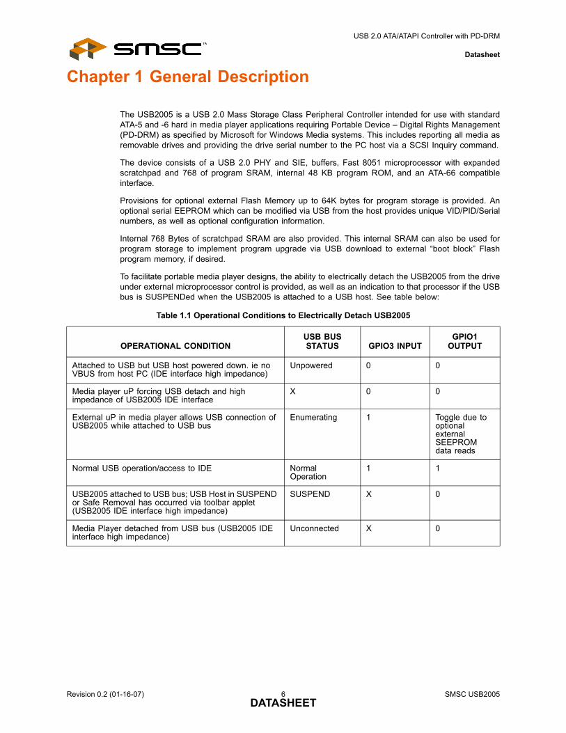
Chapter 1 General Description
The USB2005 is a USB 2.0 Mass Storage Class Peripheral Controller intended for use with standardATA-5 and -6 hard in media player applications requiring Portable Device – Digital Rights Management(PD-DRM) as specified by Microsoft for Windows Media systems. This includes reporting all media asremovable drives and providing the drive serial number to the PC host via a SCSI Inquiry command.
The device consists of a USB 2.0 PHY and SIE, buffers, Fast 8051 microprocessor with expandedscratchpad and 768 of program SRAM, internal 48 KB program ROM, and an ATA-66 compatibleinterface.
Provisions for optional external Flash Memory up to 64K bytes for program storage is provided. Anoptional serial EEPROM which can be modified via USB from the host provides unique VID/PID/Serialnumbers, as well as optional configuration information.
Internal 768 Bytes of scratchpad SRAM are also provided. This internal SRAM can also be used forprogram storage to implement program upgrade via USB download to external “boot block” Flashprogram memory, if desired.
To facilitate portable media player designs, the ability to electrically detach the USB2005 from the driveunder external microprocessor control is provided, as well as an indication to that processor if the USBbus is SUSPENDed when the USB2005 is attached to a USB host. See table below:
Table 1.1 Operational Conditions to Electrically Detach USB2005
OPERATIONAL CONDITIONUSB BUS STATUS GPIO3 INPUT
GPIO1 OUTPUT
Attached to USB but USB host powered down. ie no VBUS from host PC (IDE interface high impedance)
Unpowered 0 0
Media player uP forcing USB detach and high impedance of USB2005 IDE interface
X 0 0
External uP in media player allows USB connection of USB2005 while attached to USB bus
Enumerating 1 Toggle due to optional external SEEPROM data reads
Normal USB operation/access to IDE Normal Operation
1 1
USB2005 attached to USB bus; USB Host in SUSPEND or Safe Removal has occurred via toolbar applet(USB2005 IDE interface high impedance)
SUSPEND X 0
Media Player detached from USB bus (USB2005 IDE interface high impedance)
Unconnected X 0
USB 2.0 ATA/ATAPI Controller with PD-DRM
Datasheet
SMSC USB2005 7 Revision 0.2 (01-16-07)DATASHEET
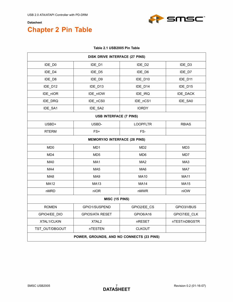
Chapter 2 Pin Table
Table 2.1 USB2005 Pin Table
DISK DRIVE INTERFACE (27 PINS)
IDE_D0 IDE_D1 IDE_D2 IDE_D3
IDE_D4 IDE_D5 IDE_D6 IDE_D7
IDE_D8 IDE_D9 IDE_D10 IDE_D11
IDE_D12 IDE_D13 IDE_D14 IDE_D15
IDE_nIOR IDE_nIOW IDE_IRQ IDE_DACK
IDE_DRQ IDE_nCS0 IDE_nCS1 IDE_SA0
IDE_SA1 IDE_SA2 IORDY
USB INTERFACE (7 PINS)
USBD+ USBD- LOOPFLTR RBIAS
RTERM FS+ FS-
MEMORY/IO INTERFACE (28 PINS)
MD0 MD1 MD2 MD3
MD4 MD5 MD6 MD7
MA0 MA1 MA2 MA3
MA4 MA5 MA6 MA7
MA8 MA9 MA10 MA11
MA12 MA13 MA14 MA15
nMRD nIOR nMWR nIOW
MISC (15 PINS)
ROMEN GPIO1/SUSPEND GPIO2/EE_CS GPIO3/VBUS
GPIO4/EE_DIO GPIO5/ATA RESET GPIO6/A16 GPIO7/EE_CLK
XTAL1/CLKIN XTAL2 nRESET nTEST/nDBGSTR
TST_OUT/DBGOUT nTESTEN CLKOUT
POWER, GROUNDS, AND NO CONNECTS (23 PINS)
USB 2.0 ATA/ATAPI Controller with PD-DRM
Datasheet
Revision 0.2 (01-16-07) 8 SMSC USB2005DATASHEET
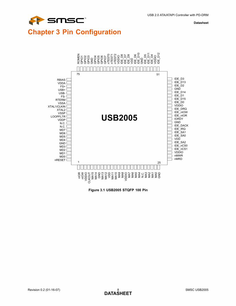
Chapter 3 Pin Configuration
Figure 3.1 USB2005 STQFP 100 Pin
nIO
RnI
OW
VD
DIO
CLK
OU
TM
A15
MA
14G
ND
MA
13M
A12
VD
DM
A11
MA
10M
A9
MA
8V
DD
IOM
A7
MA
6M
A5
MA
4N
.C.
MA
3M
A2
MA
1M
A0
GN
D
USB2005
1 25
5175R
OM
ENG
PIO
1G
PIO
2G
PIO
3G
ND
GP
IO4
GP
IO5
GP
IO6
GP
IO7
nTE
ST0
nTE
ST1
nTE
ST2
VD
DIO
IDE_
D8
IDE_
D7
IDE_
D9
VD
DID
E_D
6ID
E_D
10G
ND
IDE_
D5
IDE_
D11
IDE_
D4
VD
DIO
IDE_
D12
RBIASVDDA
FS+USB+USB-
FS-RTERM
VSSAXTAL1/CLKIN
XTAL2VSSP
LOOPFLTRVDDP
N.C.N.C.MD7MD6MD5MD4GNDMD3MD2MD1MD0
nRESET
IDE_D3IDE_D13IDE_D2GNDIDE_D14IDE_D1IDE_D15IDE_D0VDDIOIDE_DRQIDE_nIOWIDE_nIORIORDYGNDIDE_DACKIDE_IRQIDE_SA1IDE_SA0VDDIDE_SA2IDE_nCS0IDE_nCS1VDDIOnMWRnMRD
US
B 2.0 ATA
/ATAP
I Controller w
ith PD
-DR
M
Datasheet
Revision 0.2 (01-16-07)
9 S
MS
C U
SB
2005D
ATAS
HE
ET
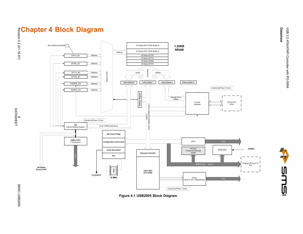
Chapter 4 Block Diagram
Figure 4.1 USB2005 Block Diagram
Da ta B
us s
USB2.0 PHY( Transciever )
FAST 8051CPU CORE
ATA-66Interface
DebugSerial 2 wire ( Data/Strobe) 2 pins
MEM/IO Bus 29pins
GPIO 7 pins
7 pi
ns
Configuration and Control
Clock Generation
XTAL
SIE( Serial Interface Engine )
Program Memory/ IOBus
Interrupt Controller
Latch phase 0 Latch phase 1 Latch phase 2
60MHz32 Bit
Future phase 3
Osc
Address
XDAT
A8
bits
( A
ddre
ss a
nd D
ata
buss
es )
64 Bytes EP0TX
64 Bytes EP0RX
64 Bytes EP1TX
64 Bytes EP1RX
Auto address generators
Add
ress
MU
X
Data @ 32 bit15MHz
SIE Control Regs
Address
Address
Address
Address
Address
EP0RX_BC
EP1RX_BC
RAMRD_A/B
EP0TX_BC
RAMWR_A/B
ATA/ATAPIDrive
32 bit 15MHz Data Buss
CLOCKOUT12 MHz
OPTIONALExternal PHY
512 Bytes EP2 TX/RX Buffer A
Add
ress
Reg
iste
r
1.25KBSRAM
768 ByteProgram/Scratchpad
SRAM
Clocked byPhase 0 Clock
Clocked byPhase 1 Clock
Clocked byPhase 2 Clock
EP1TX_BC Address
512 Bytes EP2 TX/RX Buffer B
48KB ROM ROMEN
USB 2.0 ATA/ATAPI Controller with PD-DRM
Datasheet
Chapter 5 Pin Description
Table 5.1 USB2005 Pin Descriptions
DISK DRIVE INTERFACE
IDE DMA Request IDE_DRQ IS This pin is the active high DMA request from the ATA/ATAPI interface.
IDE IO Read Strobe IDE_nIOR O20 This pin is the active low read signal for the interface.
IDE Register Address 1
IDE_SA1 O20 This pin is the register select address bit 1 signal for the ATA/ATAPI interface.
IDE Register Address 0
IDE_SA0 O20 This pin is the register select address bit 0 signal for the ATA/ATAPI interface.
IDE Register Address 2
IDE_SA2 O20 This pin is the register select address bit 2 signal for the ATA/ATAPI interface.
IDE Data IDE_D15 IO20 This pin is the bi-directional data bus bit 15 signal for the ATA/ATAPI interface.
IDE IO Write Strobe IDE_nIOW O20 This pin is active low write signal for the ATA/ATAPI interface.
IDE DMA Acknowledge
IDE_nDACK O20 This pin is the active low DMA acknowledge signal for the ATA/ATAPI interface.
IDE Interrupt Request
IDE_IRQ IS This pin is the active high interrupt request signal for the ATA/ATAPI interface.
IDE Data IDE_D13 IO20 This pin is the bi-directional data bus bit 13 signal for the ATA/ATAPI interface.
IDE Data IDE_D14 IO20 This pin is the bi-directional data bus bit 14 signal for the ATA/ATAPI interface.
IDE Chip Select 0 IDE_nCS0 O20 This pin is the active low chip select 0 signal for the ATA/ATAPI interface.
IDE Chip Select 1 0 IDE_nCS1 O20 This pin is the active low select 1 signal for the ATA/ATAPI interface.
IDE Data IDE_D[0:12] IO20 These pins are bits 0-12 of the ATA/ATAPI bi-directional data bus.
IO Ready IORDY I This pin is the active high IORDY signal from the IDE drive.
USB INTERFACE
USB Bus Data USB-USB+
IO-U These pins connect to the USB bus data signals.
USB Transceiver Filter
LOOPFLTR This pin provides the ability to supplement the internal filtering of the transceiver with an external network, if required.
USB Transceiver Bias
RBIAS A 9.09 Kohm precision resistor is attached from ground to this pin to set the transceiver’s internal bias currents.
Revision 0.2 (01-16-07) 10 SMSC USB2005DATASHEET
USB 2.0 ATA/ATAPI Controller with PD-DRM
Datasheet
Termination Resistor RTERM A precision 1.5Kohm precision resistor is attached to this pin from a 3.3V supply.
Full Speed USB Data
FS-FS+
IO-U These pins connect to the USB- and USB+ pins through 31.6 ohm series resistors.
MEMORY/IO INTERFACE
Memory Data Bus MD[7:0] IO12PU When ROMEN=0, these signals are used to transfer data between the internal CPU and the external program memory. When ROMEN=1, a weak internal pull up is activated to prevent these pins from floating.
Memory Address Bus
MA[15:0] O12 These signals address memory locations within the external memory.
Memory Write Strobe nMWR O12 Program Memory Write; active low
Memory Read Strobe
nMRD O12 Program Memory Read; active low
IO Read Strobe nIOR O12 XDATA space Read; active low
IO Write Strobe nIOW O12 XDATA space Write; active low
MISC
Crystal Input/External Clock Input
XTAL1/CLKIN
ICLKx 12Mhz Crystal or external clock input.This pin can be connected to one terminal of the crystal or can be connected to an external 12Mhz clock when a crystal is not used.
Crystal Output XTAL2 OCLKx 12Mhz CrystalThis is the other terminal of the crystal, or left open when an external clock source is used to drive XTAL1/CLKIN. It may not be used to drive any external circuitry other than the crystal circuit.
Clock Output CLKOUT O8 This pin produces a 30Mhz clock signal independent of the processor clock divider. It is held inactive and low whenever the internal processor clock is stopped or is being obtained from the ring oscillator.
Internal ROM Enable ROMEN IP When left unconnected or tied high, the USB97C202 uses the internal ROM for program execution. When tied low, an external program memory should be connected to the memory/data bus. The state of this pin latched internally on the rising edge of nRESET.
Table 5.1 USB2005 Pin Descriptions (continued)
SMSC USB2005 11 Revision 0.2 (01-16-07)DATASHEET
USB 2.0 ATA/ATAPI Controller with PD-DRM
Datasheet
General Purpose I/O GPIO[1:7] IO20 These general purpose pins may be used either as inputs, edge sensitive interrupt inputs, or outputs. When using internal ROM mode, these pins have the following assignments:GPIO1: USB SUSPEND Indicator; active highGPIO2: Optional Serial EEPROM (93LC56 type) Chip SelectGPIO3: USB VBUS Detect Input (can be used to force the IDE interface to high impedance state)GPIO4: Optional Serial EEPROM Data In/OutGPIO5: ATA Drive ResetGPIO6: A16 control line for external program Flash memory when using firmware upgrade capability (external ROM operation only)GPIO7: Optional Serial EEPROM Clock output
RESET input nRESET IS This active low signal is used by the system to reset the chip. The active low pulse should be at least 100ns wide.
Test input nTest[0:2] IP These signals are used for testing the chip. User should normally leave them unconnected. For board continuity testing, all pads (except RBIAS, FSDP, USBDP, USBDM, FSDM, RTERM, XTAL1, XTAL2, LOOPFLTR and nTEST[0:2]) are included in an XNOR chain which is enabled by pulling nTEST2 low. nIOR is the output of the chain (the chain begins at pin 2) and will reflect the toggling of a signal on each pin. Circuit board continuity of the pin solder connections after assembly can be checked in this manner
POWER, GROUNDS, AND NO CONNECTS
VDD +2.5V Core power
VDDIO +3.3V I/O power
VDDP +2.5 Analog power
VSSP Analog Ground Reference
VDDA +3.3V Analog power
VSSA Analog Ground Reference
GND Ground Reference
NC No Connect. These pins should not be connected externally.
Table 5.1 USB2005 Pin Descriptions (continued)
Revision 0.2 (01-16-07) 12 SMSC USB2005DATASHEET
USB 2.0 ATA/ATAPI Controller with PD-DRM
Datasheet
5.1 Buffer Type DescriptionsTable 5.2 USB2005 Buffer Type Descriptions
BUFFER DESCRIPTION
I Input
IS Input with Schmitt trigger
IP Input with weak pull-up
IO8 Input/Output with 8 mA drive
O8 Output with 8mA drive
O12 Output with 12mA drive
IO12PU Input/Output with 12 ma drive and controlled weak pull up
IO12 Input/Output with 12 ma drive
IO20 Input/output with 20mA drive
O20 Output with 20mA drive
O20PU Output with 20mA drive and weak pullup
ICLKx XTAL clock input
OCLKx XTAL clock output
I/O-U Defined in USB specification
SMSC USB2005 13 Revision 0.2 (01-16-07)DATASHEET
USB 2.0 ATA/ATAPI Controller with PD-DRM
Datasheet
Revision 0.2 (01-16-07) 14 SMSC USB2005DATASHEET
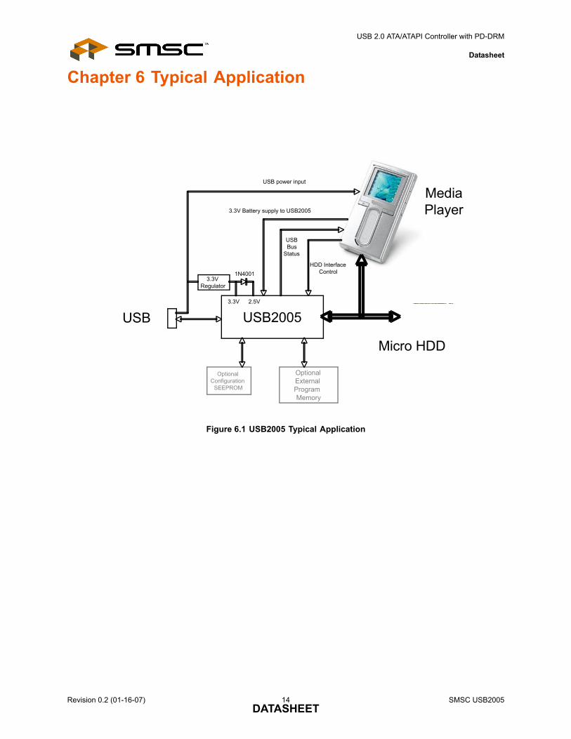
Chapter 6 Typical Application
Figure 6.1 USB2005 Typical Application
USB2005
3.3V Regulator
Micro HDD
MediaPlayer
HDD InterfaceControl
USBBus
Status
3.3V Battery supply to USB2005
USB
OptionalConfiguration
SEEPROM
OptionalExternal Program Memory
USB power input
1N4001
3.3V 2.5V
USB 2.0 ATA/ATAPI Controller with PD-DRM
Datasheet
Chapter 7 PD-DRM Usage & Description
The USB2005 is a USB 2.0 Mass Storage Class Peripheral Controller intended for use with standardATA-5 and -6 hard disk drives in media player applications requiring Portable Device – Digital RightsManagement (PD-DRM) as specified by Microsoft for Windows Media systems. This includes reportingall media as removable drives and providing the drive serial number to the PC host via the SCSIInquiry command.
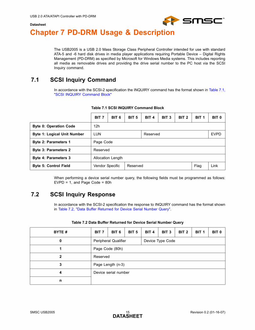
7.1 SCSI Inquiry CommandIn accordance with the SCSI-2 specification the INQUIRY command has the format shown in Table 7.1,"SCSI INQUIRY Command Block"
When performing a device serial number query, the following fields must be programmed as follows:EVPD = 1, and Page Code = 80h
7.2 SCSI Inquiry ResponseIn accordance with the SCSI-2 specification the response to INQUIRY command has the format shownin Table 7.2, "Data Buffer Returned for Device Serial Number Query".
Table 7.1 SCSI INQUIRY Command Block
BIT 7 BIT 6 BIT 5 BIT 4 BIT 3 BIT 2 BIT 1 BIT 0
Byte 0: Operation Code 12h
Byte 1: Logical Unit Number LUN Reserved EVPD
Byte 2: Parameters 1 Page Code
Byte 3: Parameters 2 Reserved
Byte 4: Parameters 3 Allocation Length
Byte 5: Control Field Vendor Specific Reserved Flag Link
Table 7.2 Data Buffer Returned for Device Serial Number Query
BYTE # BIT 7 BIT 6 BIT 5 BIT 4 BIT 3 BIT 2 BIT 1 BIT 0
0 Peripheral Qualifier Device Type Code
1 Page Code (80h)
2 Reserved
3 Page Length (n-3)
4 Device serial number
n
SMSC USB2005 15 Revision 0.2 (01-16-07)DATASHEET
USB 2.0 ATA/ATAPI Controller with PD-DRM
Datasheet
7.2.1 Device Serial Number & Page Length (Bytes 3 & 4...n)
In response to a SCSI INQUIRY Command, the USB2005 firmware will read the “Device IdentifyInformation” of an IDE drive. The Device Serial Number is created by removing all NULL code (00h)and BLANK code (20h) characters from the “Device Identify Information” response. The Device SerialNumber is reported in Byte 4...n (see Table 7.2). The number of characters of the Device SerialNumber will be reported as the Page Length (Byte 3) see Table 7.2.
As a simple example, If the Device Identify Information of an IDE drive is 713 740, then the USB2005will return 713740 as the Device Serial Number with a Page Length of 6.
Revision 0.2 (01-16-07) 16 SMSC USB2005DATASHEET
USB 2.0 ATA/ATAPI Controller with PD-DRM
Datasheet
Chapter 8 DC Parameters
8.1 Maximum Guaranteed RatingsOperating Temperature Range ............................................................................................0oC to +70oC
Storage Temperature Range............................................................................................. -55o to +150oC
Lead Temperature Range (soldering, 10 seconds) ...................................................................... +325oC
Positive Voltage on any pin, with respect to Ground........................................................................ 5.5V
Negative Voltage on any pin, with respect to Ground ..................................................................... -0.3V
Maximum VDDA, VDDIO..................................................................................................................... +4.0V
Maximum VDD, VDDP ........................................................................................................................ +3.0V
*Stresses above the specified parameters could cause permanent damage to the device. This is astress rating only and functional operation of the device at any other condition above those indicatedin the operation sections of this specification is not implied.
Note: When powering this device from laboratory or system power supplies, it is important that theAbsolute Maximum Ratings not be exceeded or device failure can result. Some power suppliesexhibit voltage spikes on their outputs when the AC power is switched on or off. In addition,voltage transients on the AC power line may appear on the DC output. When this possibilityexists, it is suggested that a clamp circuit be used.
8.2 DC Electrical Characteristics(TA = 0°C - 70°C, VDDIO, VDDA = +3.3 V ± 10%, VDD, VDDP = +2.5 V ± 10%,)
PARAMETER SYMBOL MIN TYP MAX UNITS COMMENTS
I Type Input Buffer
Low Input Level
High Input Level
VILI
VIHI 2.0
0.8 V
V
TTL Levels
ICLK Input Buffer
Low Input Level
High Input Level
VILCK
VIHCK 2.2
0.4 V
V
Input Leakage(All I and IS buffers)
Low Input Leakage
High Input Leakage
IIL
IIH
-10
-10
+10
+10
µA
µA
VIN = 0
VIN = VDDIO
SMSC USB2005 17 Revision 0.2 (01-16-07)DATASHEET
USB 2.0 ATA/ATAPI Controller with PD-DRM
Datasheet
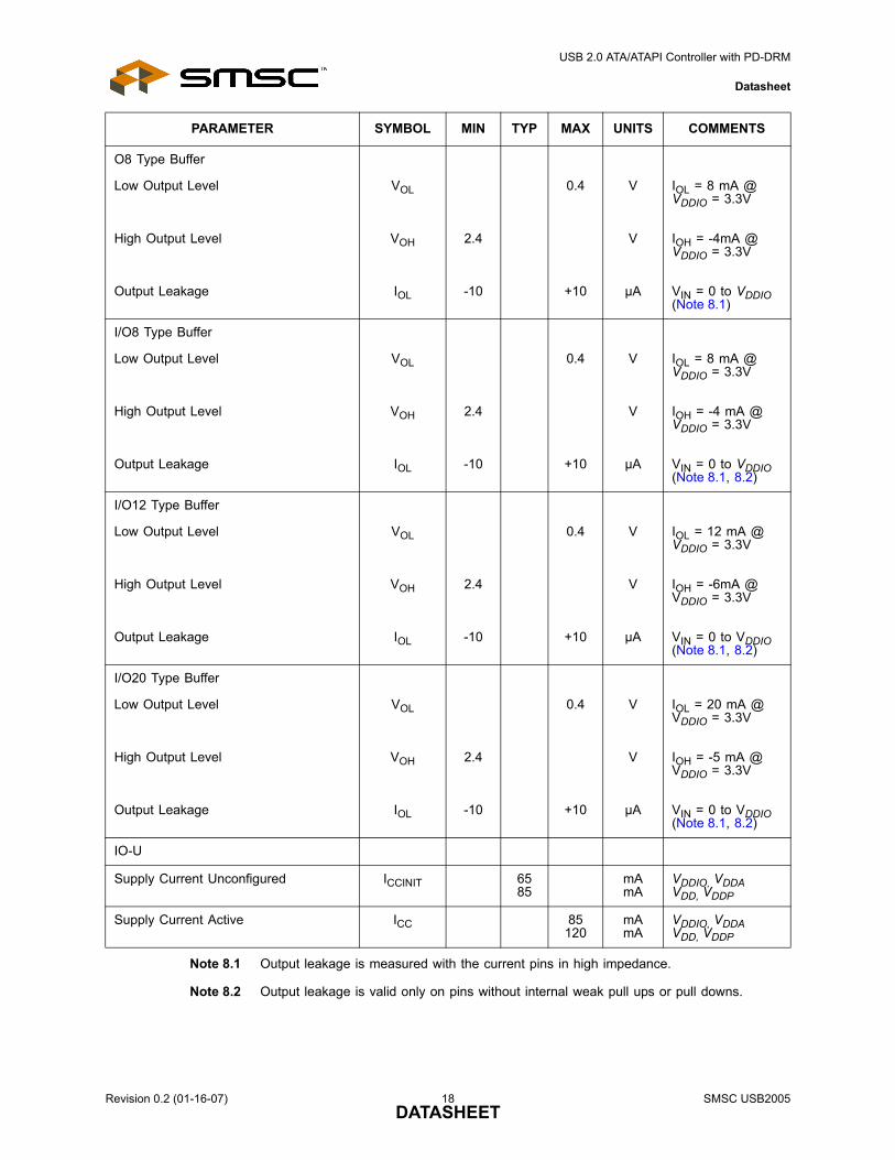
Note 8.1 Output leakage is measured with the current pins in high impedance.
Note 8.2 Output leakage is valid only on pins without internal weak pull ups or pull downs.
O8 Type Buffer
Low Output Level
High Output Level
Output Leakage
VOL
VOH
IOL
2.4
-10
0.4
+10
V
V
µA
IOL = 8 mA @ VDDIO = 3.3V
IOH = -4mA @ VDDIO = 3.3V
VIN = 0 to VDDIO(Note 8.1)
I/O8 Type Buffer
Low Output Level
High Output Level
Output Leakage
VOL
VOH
IOL
2.4
-10
0.4
+10
V
V
µA
IOL = 8 mA @ VDDIO = 3.3V
IOH = -4 mA @ VDDIO = 3.3V
VIN = 0 to VDDIO(Note 8.1, 8.2)
I/O12 Type Buffer
Low Output Level
High Output Level
Output Leakage
VOL
VOH
IOL
2.4
-10
0.4
+10
V
V
µA
IOL = 12 mA @ VDDIO = 3.3V
IOH = -6mA @ VDDIO = 3.3V
VIN = 0 to VDDIO(Note 8.1, 8.2)
I/O20 Type Buffer
Low Output Level
High Output Level
Output Leakage
VOL
VOH
IOL
2.4
-10
0.4
+10
V
V
µA
IOL = 20 mA @ VDDIO = 3.3V
IOH = -5 mA @ VDDIO = 3.3V
VIN = 0 to VDDIO(Note 8.1, 8.2)
IO-U
Supply Current Unconfigured ICCINIT 6585
mAmA
VDDIO, VDDAVDD, VDDP
Supply Current Active ICC 85120
mAmA
VDDIO, VDDAVDD, VDDP
PARAMETER SYMBOL MIN TYP MAX UNITS COMMENTS
Revision 0.2 (01-16-07) 18 SMSC USB2005DATASHEET
USB 2.0 ATA/ATAPI Controller with PD-DRM
Datasheet
CAPACITANCE TA = 25°C; fc = 1MHz; VDD = 2.5V
LIMITS
PARAMETER SYMBOL MIN TYP MAX UNIT TEST CONDITION
Clock Input Capacitance CIN 20 pF All pins except USB pins (and pins under test tied to AC ground)
Input Capacitance CIN 10 pF
Output Capacitance COUT 20 pF
SMSC USB2005 19 Revision 0.2 (01-16-07)DATASHEET
USB 2.0 ATA/ATAPI Controller with PD-DRM
Datasheet
Revision 0.2 (01-16-07) 20 SMSC USB2005DATASHEET
Chapter 9 AC Specifications
9.1 ATA/ATAPIThe USB2005 conforms to all timing diagrams and specifications for ATAPI-5 as set forth in theT13/1321D Revision 3 NCITS specification. Please refer to this specification for more information.
9.2 USB 2.0 TimingThe USB2005 conforms to all timing diagrams and specifications for USB peripheral silicon buildingblocks as set forth in the USB-IF USB 2.0 specification. Please refer to this specification for moreinformation.
US
B 2.0 ATA
/ATAP
I Controller w
ith PD
-DR
M
Datasheet
Revision 0.2 (01-16-07)
21 S
MS
C U
SB
2005D
ATAS
HE
ET
Chapter 10 Package Outline
Figure 10.1 USB2005 100 Pin STQFP Package (12x12x1.4 mm body, 14x14 mm footprint)
Eb
D1D
E1
NOTES:1. ALL DIMENSIONS ARE IN MILLIMETER.2. TRUE POSITION SPREAD TOLERANCE OF EACH LEAD IS ± 0.035mm MAXIMUM.3. DIMENSIONS "D1" AND "E1" DO NOT INCLUDE MOLD PROTRUSIONS. MAXIMUM ALLOWED PROTRUSION IS 0.25 mm PER SIDE.4. DIMENSION "L" IS MEASURED AT THE GAUGE PLANE, 0.25mm ABOVE THE SEATING PLANE.5. DETAILS ON PIN 1 IDENTIFIER ARE OPTIONAL BUT MUST BE LOCATED WITHIN THE ZONE INDICATED.
STD COMPLIANCE
INTERPRET DIM AND TOL PER ASME Y14.5M - 1994
DWG NUMBER
PRINT WITH "SCALE TO FIT" DO NOT SCALE DRAWING
MATERIAL
FINISH
APPROVED
CHECKED
DRAWN
SCALE SHEET
REV
80 ARKAY DRIVEHAUPPAUGE, NY 11788USAANGULAR
UNLESS OTHERWISE SPECIFIEDDIMENSIONS ARE IN MILLIMETERS AND TOLERANCES ARE:
DECIMALX.XX.XXX.XXX
THIRD ANGLE PROJECTION
NAME DATE
TITLE
REVISION DATEDESCRIPTION
REVISION HISTORY
RELEASED BY
JEDEC: MS-026 (D)
PACKAGE OUTLINE
1:1
-
-
S.K.ILIEV
S.K.ILIEV
S.K.ILIEV
12/17/04
12/17/04
12/17/04
100 STQFP-12x12x1.4mm BODY-0.4mm PITCH
MO-100-STQFP-12x12x1.4
1 OF 1
C
±1°±0.1±0.05±0.025
R1
R2
- SEE SPEC FRONT PAGE FOR REVISION HISTORY - -
e
E1/4
D1/4
TOP VIEW
SIDE VIEW
DETAIL "A"
3-D VIEW
3
3
2
5
A1
A2 A
c
C
ccc C
SEE DETAIL "A"
L
L1
SEATING PLANE
0.250°-7°
GAUGE PLANE
4