Embed Size (px)
Citation preview
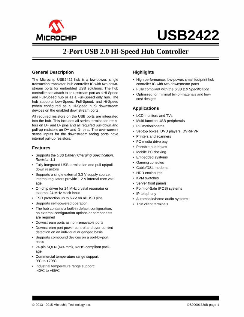
USB24222-Port USB 2.0 Hi-Speed Hub Controller
General Description
The Microchip USB2422 hub is a low-power, singletransaction translator, hub controller IC with two down-stream ports for embedded USB solutions. The hubcontroller can attach to an upstream port as a Hi-Speedand Full-Speed hub or as a Full-Speed only hub. Thehub supports Low-Speed, Full-Speed, and Hi-Speed(when configured as a Hi-Speed hub) downstreamdevices on the enabled downstream ports.
All required resistors on the USB ports are integratedinto the hub. This includes all series termination resis-tors on D+ and D- pins and all required pull-down andpull-up resistors on D+ and D- pins. The over-currentsense inputs for the downstream facing ports haveinternal pull-up resistors.
Features
• Supports the USB Battery Charging Specification, Revision 1.1
• Fully integrated USB termination and pull-up/pull-down resistors
• Supports a single external 3.3 V supply source; internal regulators provide 1.2 V internal core volt-age
• On-chip driver for 24 MHz crystal resonator or external 24 MHz clock input
• ESD protection up to 6 kV on all USB pins
• Supports self-powered operation
• The hub contains a built-in default configuration; no external configuration options or components are required
• Downstream ports as non-removable ports
• Downstream port power control and over-current detection on an individual or ganged basis
• Supports compound devices on a port-by-port basis
• 24-pin SQFN (4x4 mm), RoHS-compliant pack-age
• Commercial temperature range support: 0ºC to +70ºC
• Industrial temperature range support: -40ºC to +85ºC
Highlights
• High performance, low-power, small footprint hub controller IC with two downstream ports
• Fully compliant with the USB 2.0 Specification
• Optimized for minimal bill-of-materials and low-cost designs
Applications
• LCD monitors and TVs
• Multi-function USB peripherals
• PC motherboards
• Set-top boxes, DVD players, DVR/PVR
• Printers and scanners
• PC media drive bay
• Portable hub boxes
• Mobile PC docking
• Embedded systems
• Gaming consoles
• Cable/DSL modems
• HDD enclosures
• KVM switches
• Server front panels
• Point-of-Sale (POS) systems
• IP telephony
• Automobile/home audio systems
• Thin client terminals
2013 - 2015 Microchip Technology Inc. DS00001726B-page 1
USB2422
TO OUR VALUED CUSTOMERS
It is our intention to provide our valued customers with the best documentation possible to ensure successful use of your Microchipproducts. To this end, we will continue to improve our publications to better suit your needs. Our publications will be refined andenhanced as new volumes and updates are introduced.
If you have any questions or comments regarding this publication, please contact the Marketing Communications Department viaE-mail at [email protected]. We welcome your feedback.
Most Current Data SheetTo obtain the most up-to-date version of this data sheet, please register at our Worldwide Web site at:
http://www.microchip.com
You can determine the version of a data sheet by examining its literature number found on the bottom outside corner of any page. The last character of the literature number is the version number, (e.g., DS30000000A is version A of document DS30000000).
ErrataAn errata sheet, describing minor operational differences from the data sheet and recommended workarounds, may exist for cur-rent devices. As device/documentation issues become known to us, we will publish an errata sheet. The errata will specify therevision of silicon and revision of document to which it applies.
To determine if an errata sheet exists for a particular device, please check with one of the following:• Microchip’s Worldwide Web site; http://www.microchip.com• Your local Microchip sales office (see last page)
When contacting a sales office, please specify which device, revision of silicon and data sheet (include -literature number) you areusing.
Customer Notification SystemRegister on our web site at www.microchip.com to receive the most current information on all of our products.
DS00001726B-page 2 2013 - 2015 Microchip Technology Inc.

2013 - 2015 Microchip Technology Inc. DS00001726B-page 3
USB2422
Table of Contents
1.0 Block Diagram ................................................................................................................................................................................. 42.0 Pin Descriptions .............................................................................................................................................................................. 63.0 Battery Charging Support ............................................................................................................................................................. 144.0 Configuration Options ................................................................................................................................................................... 165.0 DC Parameters ............................................................................................................................................................................. 356.0 AC Specifications .......................................................................................................................................................................... 387.0 Package Outline ............................................................................................................................................................................ 40Appendix A: Acronyms ........................................................................................................................................................................ 41Appendix B: References ..................................................................................................................................................................... 42Appendix C: Data Sheet Revision History .......................................................................................................................................... 43The Microchip Web Site ...................................................................................................................................................................... 44Customer Change Notification Service ............................................................................................................................................... 44Customer Support ............................................................................................................................................................................... 44Product Identification System ............................................................................................................................................................. 45

USB2422
1.0 BLOCK DIAGRAM
FIGURE 1-1: USB2422 BLOCK DIAGRAM
To UpstreamVBUS
3.3V
Upstream PHY
Upstream USB Data
Repeater ControllerSIE
Serial Interface
PLL
24 MHz Crystal
To SMBus Master
Routing & Port Re-Ordering Logic
SMBCLKSMBDATA
Port Controller
Bus-Power Detect/VBUS
Pulse
TT
PHY#1
Port #1OC
SenseSwitch Driver
PHY#2
Port #2OC
SenseSwitch Driver
USB DataDownstream
OC SenseSwitch
USB DataDownstream
OC SenseSwitch
CRFILT PLLFILT
1.2V Reg
DS00001726B-page 4 2013 - 2015 Microchip Technology Inc.
USB2422
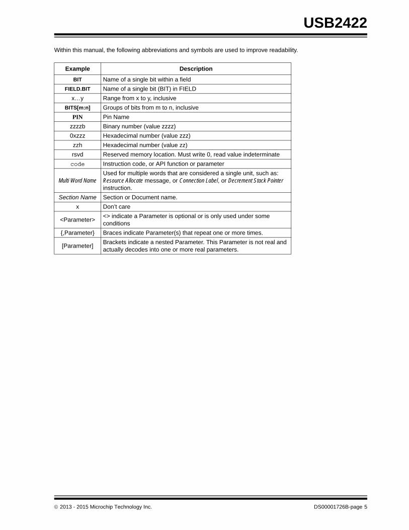
Within this manual, the following abbreviations and symbols are used to improve readability.
Example Description
BIT Name of a single bit within a field
FIELD.BIT Name of a single bit (BIT) in FIELD
x…y Range from x to y, inclusive
BITS[m:n] Groups of bits from m to n, inclusive
PIN Pin Name
zzzzb Binary number (value zzzz)
0xzzz Hexadecimal number (value zzz)
zzh Hexadecimal number (value zz)
rsvd Reserved memory location. Must write 0, read value indeterminate
code Instruction code, or API function or parameter
Multi Word NameUsed for multiple words that are considered a single unit, such as:Resource Allocate message, or Connection Label, or Decrement Stack Pointer instruction.
Section Name Section or Document name.
x Don’t care
<Parameter><> indicate a Parameter is optional or is only used under some conditions
{,Parameter} Braces indicate Parameter(s) that repeat one or more times.
[Parameter]Brackets indicate a nested Parameter. This Parameter is not real and actually decodes into one or more real parameters.
2013 - 2015 Microchip Technology Inc. DS00001726B-page 5
USB2422
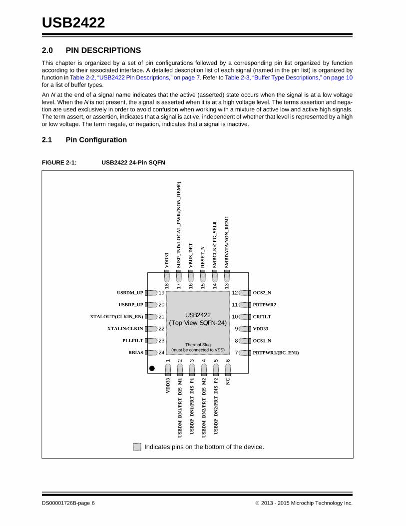
2.0 PIN DESCRIPTIONS
This chapter is organized by a set of pin configurations followed by a corresponding pin list organized by functionaccording to their associated interface. A detailed description list of each signal (named in the pin list) is organized byfunction in Table 2-2, “USB2422 Pin Descriptions,” on page 7. Refer to Table 2-3, “Buffer Type Descriptions,” on page 10for a list of buffer types.
An N at the end of a signal name indicates that the active (asserted) state occurs when the signal is at a low voltagelevel. When the N is not present, the signal is asserted when it is at a high voltage level. The terms assertion and nega-tion are used exclusively in order to avoid confusion when working with a mixture of active low and active high signals.The term assert, or assertion, indicates that a signal is active, independent of whether that level is represented by a highor low voltage. The term negate, or negation, indicates that a signal is inactive.
2.1 Pin Configuration
FIGURE 2-1: USB2422 24-Pin SQFN
Thermal Slug(must be connected to VSS)
12
11
10
9
8
7
USBDP_UP
19
XTALOUT/(CLKIN_EN)
20
XTALIN/CLKIN
21
RBIAS 24
23PLLFILT
22
1V
DD
33
2
USB
DP
_DN
1/P
RT
_DIS
_P1
3
USB
DM
_DN
2/P
RT
_DIS
_M2
4
USB
DP
_DN
2/P
RT
_DIS
_P2
5 6
USB
DM
_DN
1/P
RT
_DIS
_M1
NC
USBDM_UP
17SU
SP
_IN
D/L
OC
AL
_PW
R/(
NO
N_R
EM
0)
16V
BU
S_D
ET
RE
SE
T_N
15 14SM
BC
LK
/CF
G_S
EL
0
VD
D33
18 13SM
BD
AT
A/N
ON
_RE
M1
Indicates pins on the bottom of the device.
OCS1_N
PRTPWR1/(BC_EN1)
VDD33
CRFILT
PRTPWR2
OCS2_N
USB2422(Top View SQFN-24)
DS00001726B-page 6 2013 - 2015 Microchip Technology Inc.
USB2422
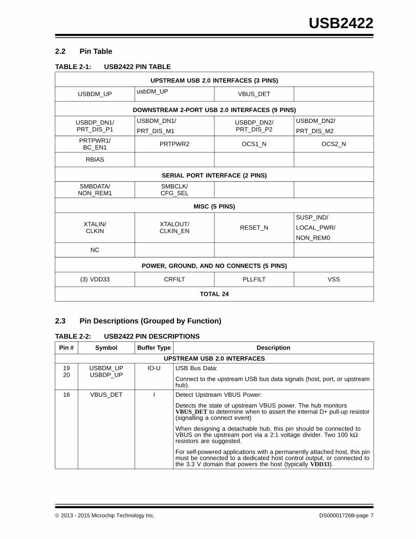
2.2 Pin Table
2.3 Pin Descriptions (Grouped by Function)
TABLE 2-1: USB2422 PIN TABLE
UPSTREAM USB 2.0 INTERFACES (3 PINS)
USBDM_UP usbDM_UP VBUS_DET
DOWNSTREAM 2-PORT USB 2.0 INTERFACES (9 PINS)
USBDP_DN1/PRT_DIS_P1
USBDM_DN1/
PRT_DIS_M1USBDP_DN2/PRT_DIS_P2
USBDM_DN2/
PRT_DIS_M2
PRTPWR1/BC_EN1 PRTPWR2 OCS1_N OCS2_N
RBIAS
SERIAL PORT INTERFACE (2 PINS)
SMBDATA/NON_REM1
SMBCLK/CFG_SEL
MISC (5 PINS)
XTALIN/CLKIN
XTALOUT/CLKIN_EN RESET_N
SUSP_IND/
LOCAL_PWR/
NON_REM0
NC
POWER, GROUND, AND NO CONNECTS (5 PINS)
(3) VDD33 CRFILT PLLFILT VSS
TOTAL 24
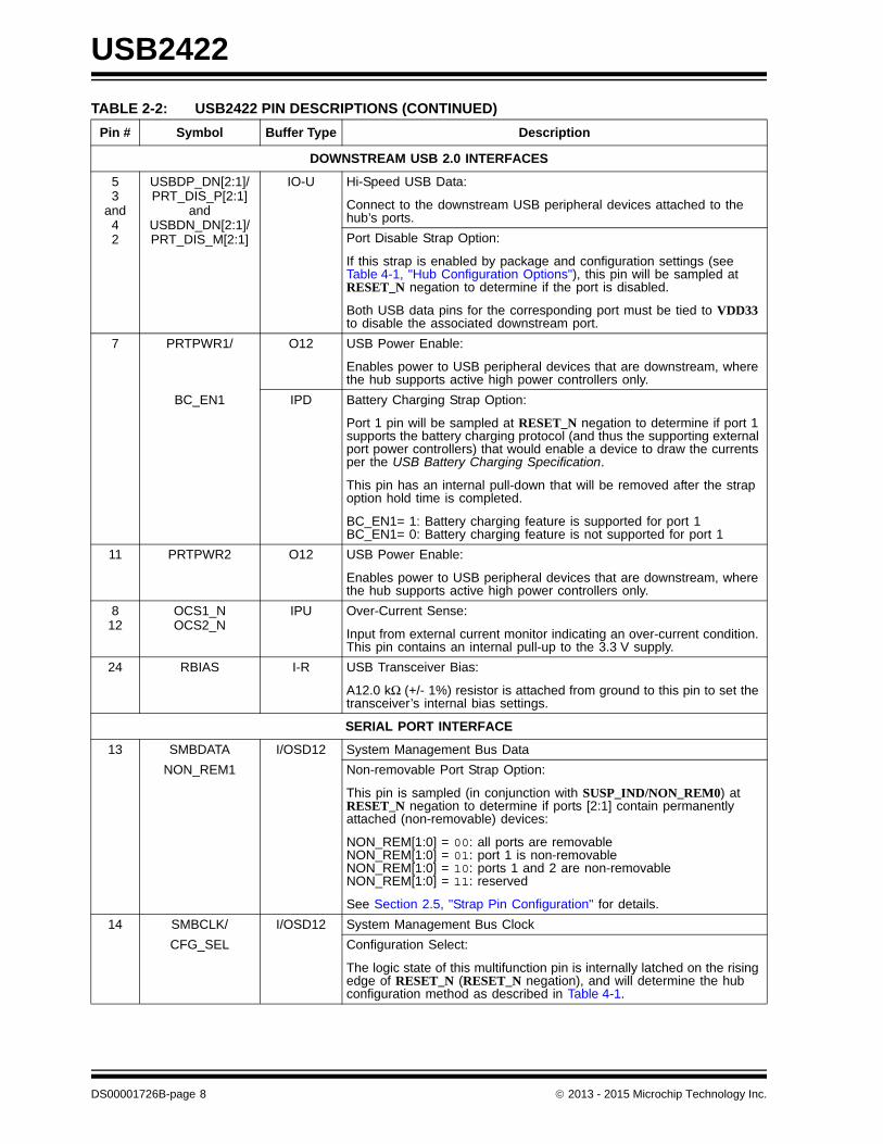
TABLE 2-2: USB2422 PIN DESCRIPTIONS
Pin # Symbol Buffer Type Description
UPSTREAM USB 2.0 INTERFACES
1920
USBDM_UPUSBDP_UP
IO-U USB Bus Data:
Connect to the upstream USB bus data signals (host, port, or upstream hub).
16 VBUS_DET I Detect Upstream VBUS Power:
Detects the state of upstream VBUS power. The hub monitors VBUS_DET to determine when to assert the internal D+ pull-up resistor (signalling a connect event)
When designing a detachable hub, this pin should be connected to VBUS on the upstream port via a 2:1 voltage divider. Two 100 kΩ resistors are suggested.
For self-powered applications with a permanently attached host, this pin must be connected to a dedicated host control output, or connected to the 3.3 V domain that powers the host (typically VDD33).
2013 - 2015 Microchip Technology Inc. DS00001726B-page 7
USB2422
DOWNSTREAM USB 2.0 INTERFACES
53
and42
USBDP_DN[2:1]/PRT_DIS_P[2:1]
andUSBDN_DN[2:1]/PRT_DIS_M[2:1]
IO-U Hi-Speed USB Data:
Connect to the downstream USB peripheral devices attached to the hub’s ports.
Port Disable Strap Option:
If this strap is enabled by package and configuration settings (see Table 4-1, "Hub Configuration Options"), this pin will be sampled at RESET_N negation to determine if the port is disabled.
Both USB data pins for the corresponding port must be tied to VDD33 to disable the associated downstream port.
7 PRTPWR1/ O12 USB Power Enable:
Enables power to USB peripheral devices that are downstream, where the hub supports active high power controllers only.
BC_EN1 IPD Battery Charging Strap Option:
Port 1 pin will be sampled at RESET_N negation to determine if port 1 supports the battery charging protocol (and thus the supporting external port power controllers) that would enable a device to draw the currents per the USB Battery Charging Specification.
This pin has an internal pull-down that will be removed after the strap option hold time is completed.
BC_EN1= 1: Battery charging feature is supported for port 1BC_EN1= 0: Battery charging feature is not supported for port 1
11 PRTPWR2 O12 USB Power Enable:
Enables power to USB peripheral devices that are downstream, where the hub supports active high power controllers only.
812
OCS1_NOCS2_N
IPU Over-Current Sense:
Input from external current monitor indicating an over-current condition. This pin contains an internal pull-up to the 3.3 V supply.
24 RBIAS I-R USB Transceiver Bias:
A12.0 kΩ (+/- 1%) resistor is attached from ground to this pin to set the transceiver’s internal bias settings.
SERIAL PORT INTERFACE
13 SMBDATA I/OSD12 System Management Bus Data
NON_REM1 Non-removable Port Strap Option:
This pin is sampled (in conjunction with SUSP_IND/NON_REM0) at RESET_N negation to determine if ports [2:1] contain permanently attached (non-removable) devices:
NON_REM[1:0] = 00: all ports are removableNON_REM[1:0] = 01: port 1 is non-removableNON_REM[1:0] = 10: ports 1 and 2 are non-removableNON_REM[1:0] = 11: reserved
See Section 2.5, "Strap Pin Configuration" for details.
14 SMBCLK/ I/OSD12 System Management Bus Clock
CFG_SEL Configuration Select:
The logic state of this multifunction pin is internally latched on the rising edge of RESET_N (RESET_N negation), and will determine the hub configuration method as described in Table 4-1.
TABLE 2-2: USB2422 PIN DESCRIPTIONS (CONTINUED)
Pin # Symbol Buffer Type Description
DS00001726B-page 8 2013 - 2015 Microchip Technology Inc.
USB2422
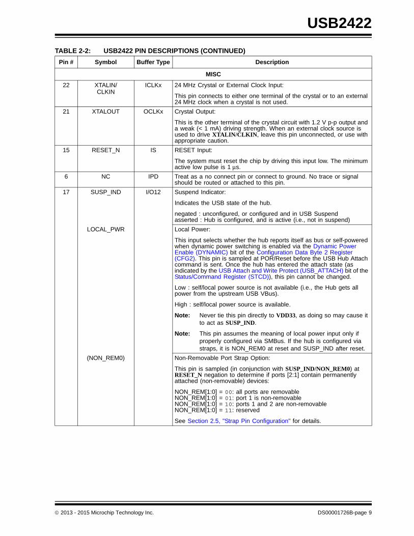
MISC
22 XTALIN/CLKIN
ICLKx 24 MHz Crystal or External Clock Input:
This pin connects to either one terminal of the crystal or to an external 24 MHz clock when a crystal is not used.
21 XTALOUT OCLKx Crystal Output:
This is the other terminal of the crystal circuit with 1.2 V p-p output and a weak (< 1 mA) driving strength. When an external clock source is used to drive XTALIN/CLKIN, leave this pin unconnected, or use with appropriate caution.
15 RESET_N IS RESET Input:
The system must reset the chip by driving this input low. The minimum active low pulse is 1 μs.
6 NC IPD Treat as a no connect pin or connect to ground. No trace or signal should be routed or attached to this pin.
17 SUSP_IND I/O12 Suspend Indicator:
Indicates the USB state of the hub.
negated : unconfigured, or configured and in USB Suspendasserted : Hub is configured, and is active (i.e., not in suspend)
LOCAL_PWR Local Power:
This input selects whether the hub reports itself as bus or self-powered when dynamic power switching is enabled via the Dynamic Power Enable (DYNAMIC) bit of the Configuration Data Byte 2 Register (CFG2). This pin is sampled at POR/Reset before the USB Hub Attach command is sent. Once the hub has entered the attach state (as indicated by the USB Attach and Write Protect (USB_ATTACH) bit of the Status/Command Register (STCD)), this pin cannot be changed.
Low : self/local power source is not available (i.e., the Hub gets all power from the upstream USB VBus).
High : self/local power source is available.
Note: Never tie this pin directly to VDD33, as doing so may cause it to act as SUSP_IND.
Note: This pin assumes the meaning of local power input only if properly configured via SMBus. If the hub is configured via straps, it is NON_REM0 at reset and SUSP_IND after reset.
(NON_REM0) Non-Removable Port Strap Option:
This pin is sampled (in conjunction with SUSP_IND/NON_REM0) at RESET_N negation to determine if ports [2:1] contain permanently attached (non-removable) devices:
NON_REM[1:0] = 00: all ports are removableNON_REM[1:0] = 01: port 1 is non-removableNON_REM[1:0] = 10: ports 1 and 2 are non-removableNON_REM[1:0] = 11: reserved
See Section 2.5, "Strap Pin Configuration" for details.
TABLE 2-2: USB2422 PIN DESCRIPTIONS (CONTINUED)
Pin # Symbol Buffer Type Description
2013 - 2015 Microchip Technology Inc. DS00001726B-page 9

USB2422
2.4 Buffer Type Descriptions
2.5 Strap Pin Configuration
If a pin's strap function is enabled through hub configuration selection (Table 4-1), the strap pins must be pulled eitherhigh or low using the values provided in Table 2-4. Each strap option is dependent on the pin’s buffer type, as outlinedin the sections that follow.
POWER, GROUND, and NO CONNECTS
19
18
VDD33 3.3 V power to the chip.
A 1.0 μF low-ESR capacitor to VSS is required on pin 9 as close as possible to the pin. A 0.1 μF low-ESR capacitor to VSS is required on pin 1 as close as possible to the pin.
10 CRFILT VDD Core Regulator Filter Capacitor:
This pin requires a 1.0 μF low-ESR capacitor to VSS for proper operation.
23 PLLFILT PLL Regulator Filter Capacitor:
This pin can have up to a 0.1 μF low-ESR capacitor to VSS, or be left unconnected.
VSS Ground Pad/ePad:
The package slug is the only VSS for the device and must be tied to ground with multiple vias.
TABLE 2-3: BUFFER TYPE DESCRIPTIONS
Buffer Description
I/O Input/Output
IPD Input with internal weak pull-down resistor
IPU Input with internal weak pull-up resistor
IS Input with Schmitt trigger
I/O12 Input/Output buffer with 12 mA sink and 12 mA source
ICLKx XTAL clock input
OCLKx XTAL clock output
I-R RBIAS
I/O-U Analog Input/Output defined in USB specification
TABLE 2-4: STRAP OPTION SUMMARY
Strap Option Resistor Value Buffer Type Notes
Non-Removable 47 - 100 kΩ I/O
Internal Pull-Down (IPD)10 kΩ IPD
• Only applicable to port power pins
• Contains a built-in resistor
LED 47 - 100 kΩ I/O
TABLE 2-2: USB2422 PIN DESCRIPTIONS (CONTINUED)
Pin # Symbol Buffer Type Description
DS00001726B-page 10 2013 - 2015 Microchip Technology Inc.
USB2422
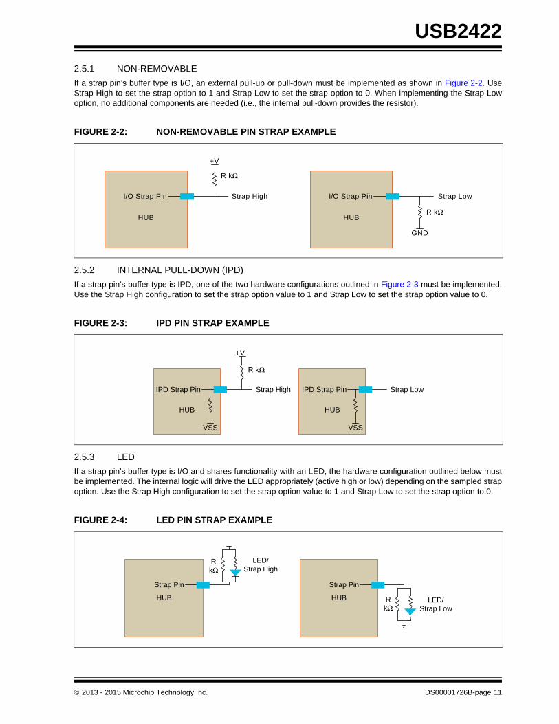
2.5.1 NON-REMOVABLE
If a strap pin’s buffer type is I/O, an external pull-up or pull-down must be implemented as shown in Figure 2-2. UseStrap High to set the strap option to 1 and Strap Low to set the strap option to 0. When implementing the Strap Lowoption, no additional components are needed (i.e., the internal pull-down provides the resistor).
2.5.2 INTERNAL PULL-DOWN (IPD)
If a strap pin’s buffer type is IPD, one of the two hardware configurations outlined in Figure 2-3 must be implemented.Use the Strap High configuration to set the strap option value to 1 and Strap Low to set the strap option value to 0.
2.5.3 LED
If a strap pin’s buffer type is I/O and shares functionality with an LED, the hardware configuration outlined below mustbe implemented. The internal logic will drive the LED appropriately (active high or low) depending on the sampled strapoption. Use the Strap High configuration to set the strap option value to 1 and Strap Low to set the strap option to 0.
FIGURE 2-2: NON-REMOVABLE PIN STRAP EXAMPLE
FIGURE 2-3: IPD PIN STRAP EXAMPLE
FIGURE 2-4: LED PIN STRAP EXAMPLE
HUB
I/O Strap Pin Strap High
+V
HUB
I/O Strap Pin Strap Low
GND
R kΩ
R kΩ
HUBHUB
IPD Strap Pin Strap High
R kΩ
+V
VSS
IPD Strap Pin Strap Low
VSS
HUB
Strap Pin
LED/Strap High
HUB
Strap Pin
LED/Strap Low
R kΩ
R kΩ
2013 - 2015 Microchip Technology Inc. DS00001726B-page 11
USB2422
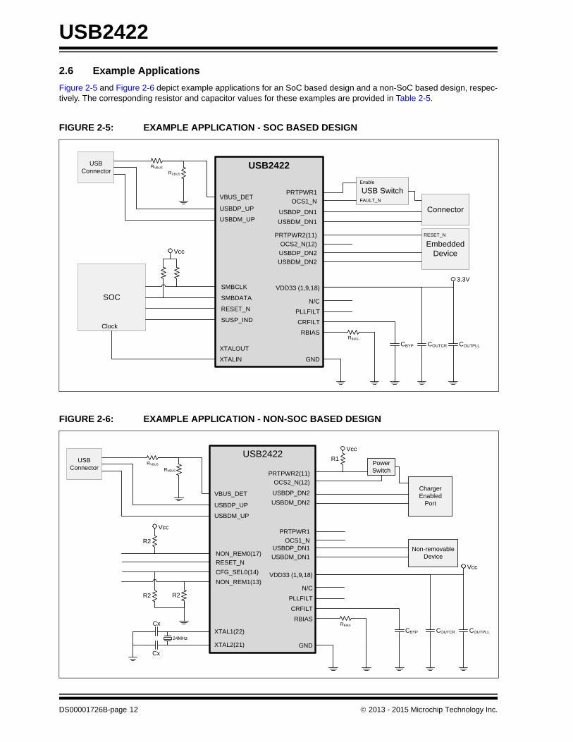
2.6 Example Applications
Figure 2-5 and Figure 2-6 depict example applications for an SoC based design and a non-SoC based design, respec-tively. The corresponding resistor and capacitor values for these examples are provided in Table 2-5.
FIGURE 2-5: EXAMPLE APPLICATION - SOC BASED DESIGN
FIGURE 2-6: EXAMPLE APPLICATION - NON-SOC BASED DESIGN
Embedded Device
SOC
USB2422
SMBCLK
SMBDATA
RESET_N
XTALOUT
XTALIN
SUSP_IND
RBIAS
VDD33 (1,9,18)
PLLFILT
CRFILT
N/C
PRTPWR1
OCS1_N
USBDP_DN1
USBDM_DN1
PRTPWR2(11)
OCS2_N(12)
USBDP_DN2
USBDM_DN2
GND
RBIAS
CBYP COUTCR COUTPLL
Vcc
USB SwitchEnable
FAULT_N
RESET_N
Clock
VBUS_DET
USBDP_UP
USBDM_UP
Connector
3.3V
USB Connector RVBUS
RVBUS
USB2422
VBUS_DET
USBDP_UP
USBDM_UP
CFG_SEL0(14)
NON_REM1(13)
RESET_N
XTAL1(22)
XTAL2(21)
NON_REM0(17)
RBIAS
VDD33 (1,9,18)
PLLFILT
CRFILT
N/C
PRTPWR2(11)
OCS2_N(12)
USBDP_DN2
USBDM_DN2
PRTPWR1
OCS1_NUSBDP_DN1
USBDM_DN1
GND
R2R2
RBIAS
CBYP COUTCR COUTPLL
USB Connector RVBUS
RVBUS
R2
Vcc
Vcc
24MHz
Cx
Cx
R1
Vcc
Non-removable Device
Charger Enabled
Port
Power Switch
DS00001726B-page 12 2013 - 2015 Microchip Technology Inc.
USB2422
Note 2-1 COUTCR should be placed as close as possible to pin 9
Note 2-2 COUTPLL should be placed as close as possible to pin 1
TABLE 2-5: EXAMPLE APPLICATIONS - RESISTOR/CAPACITOR VALUES
Designator Value
R1 20 kΩR2 50 kΩCx 18 pF
CBYP 1.0 uF
COUTCR 1.0 uF(Note 2-1)
COUTPLL 0.1 uF(Note 2-2)
RBIAS 12 kΩRVBUS 100 kΩ
2013 - 2015 Microchip Technology Inc. DS00001726B-page 13
USB2422
3.0 BATTERY CHARGING SUPPORT
The USB2422 hub provides support for battery charging devices on a per port basis in compliance with the USB BatteryCharging Specification, Revision 1.1. The hub can be configured to individually enable each downstream port for batterycharging support either via pin strapping (Port 1 only) as illustrated in Figure 3-1 or by setting the corresponding config-uration bits via SMBus (Section 4.1 on page 16).
3.1 USB Battery Charging
A downstream port enabled for battery charging turns on port power as soon as the power on reset and hardware con-figuration process has completed. The hub does not need to be enumerated nor does VBUS_DET need to be assertedfor the port power to be enabled. These conditions allow battery charging in S3, S4, and S5 system power states as wellas in the fully operational state. The USB Battery Charging Specification does not interfere with standard USB operation,which allows a device to perform battery charging at any time.
A port that supports battery charging must be able to support 1.5 amps of current on VBUS. Standard USB port powercontrollers typically only allow for 0.8 amps of current before detecting an over-current condition. Therefore, the 5 voltpower supply, port power controller, or over-current protection devices must be chosen to handle the larger currentdemand compared to standard USB hub designs.
3.1.1 SPECIAL BEHAVIOR OF PRTPWR PINS
The USB2422 enables VBUS by asserting the port power (PRTPWR[2:1]) as soon as the hardware configuration pro-cess has completed. If the port detects an over-current condition, PRTPWR[2:1] will be turned off to protect the circuitryfrom overloading. If an over-current condition is detected when the hub is not enumerated, PRTPWR[2:1] can only beturned on from the host or if RESET_N is toggled. These behaviors provide battery charging even when the hub is notenumerated and protect the hub from sustained short circuit conditions. If the short circuit condition persists when thehub is plugged into a host system the user is notified that a port has an over-current condition. Otherwise PRTPWR[2:1]turned on by the host system and the ports operate normally.
FIGURE 3-1: BATTERY CHARGING VIA EXTERNAL POWER SUPPLY
Note: RSTRAP enables battery charging.
USB2422
USB Port Power
Controller
IN
EN
FLAG
VBUS
5.0 V3.3 V
RSTRAP
PRTPWR1
OCSx_N
DS00001726B-page 14 2013 - 2015 Microchip Technology Inc.

USB2422
3.2 Battery Charging Configuration
The battery charging option can be configured in one of two ways:
• When the hub is brought up in the default configuration with strapping options enabled, with the PRTP-WR1/BC_EN1 pin configured (Port 1 only). See the following sections for details:
- Section 2.3, "Pin Descriptions (Grouped by Function)," on page 7
- Section 2.5, "Strap Pin Configuration," on page 10
• When the hub is initialized for configuration over SMBus.
3.2.1 BATTERY CHARGING ENABLED VIA SMBUS
Register memory map location 0xD0 is allocated for battery charging support. The Battery Charging register at location0xD0 starting from bit 1 enables battery charging for each downstream port when asserted. Bit 1 represents port 1, andbit 2 represents port 2. Each port that has battery charging enabled asserts the corresponding PRTPWR[2:1] pin.
2013 - 2015 Microchip Technology Inc. DS00001726B-page 15
USB2422
4.0 CONFIGURATION OPTIONS
Microchip’s USB 2.0 hub is fully compliant with the USB Specification [1]. Refer to Chapter 10 (Hub Specification) forgeneral details regarding hub operation and functionality.
The hub provides one Transaction Translator (TT) that is shared by both downstream ports (defined as Single-TT con-figuration). The TT contains 4 non-periodic buffers.
4.1 Hub Configuration
The USB2422 only supports internal defaults with the exception of the non-removable strap option (usingNON_REM[1:0]). The hub internal default settings are as follows:
• Internal Default Configuration without over-rides
• Strap options enabled
• Self-powered operation enabled
• Individual power switching
• Individual over-current sensing
4.2 Resets
There are two device resets: a hardware reset via RESET_N, and a USB Bus Reset.
4.2.1 EXTERNAL HARDWARE RESET_N
A valid hardware reset is defined as assertion of RESET_N for a minimum of 1 μs after all power supplies are withinoperating range. While reset is asserted, the hub (and its associated external circuitry) consumes less than 500 μA ofcurrent from the upstream USB power source.
Assertion of RESET_N causes the following:
1. All downstream ports are disabled.
2. The PRTPWR power to downstream devices is turned on when battery charging is enabled for a specific port,and removed when battery charging is disabled for a specific port.
3. The PHYs are disabled, and the differential pairs will be in a high-impedance state.
4. All transactions immediately terminate; no states are saved.
5. All internal registers return to the default state (in most cases, 00h).
6. The external crystal oscillator is halted.
7. The PLL is halted.
TABLE 4-1: HUB CONFIGURATION OPTIONS
CFG_SEL Description
0 Default configuration:• Strap options enabled
• Hub descriptors indicate the hub as “self-powered”
1 The hub is configured externally over SMBus (as an SMBus slave device with address 0101100b):• Strap options disabled
• Self-powered or bus-powered depending on register settings
• All registers configured over SMBus
DS00001726B-page 16 2013 - 2015 Microchip Technology Inc.
USB2422
4.2.1.1 Hub Configuration Timing for Strapping Option
4.2.2 USB BUS RESET
In response to the upstream port signaling a reset to the hub, the hub does the following:
1. Sets default address to 0.
2. Sets configuration to unconfigured.
3. The PRTPWR power to downstream devices is turned on when battery charging is enabled for a specific port,and removed when battery charging is disabled for a specific port.
4. Clears all TT buffers.
5. Moves device from suspended to active (if suspended).
6. Complies with Section 11.10 of the USB 2.0 Specification for behavior after completion of the reset sequence.The host then configures the hub and the hub’s downstream port devices in accordance with the specification.
The hub does not propagate the upstream USB reset to downstream devices.
FIGURE 4-1: HUB CONFIGURATION TIMING
TABLE 4-2: HUB CONFIGURATION TIMING
Name Description MIN TYP MAX Units
t1 RESET_N asserted 1 μsec
t2 Strap setup time 16.7 nsec
t3 Strap hold time 16.7 1400 nsec
t4 Hub outputs driven to inactive logic states 1.5 2 μsec
t5 USB attach (See Note) 3 μsec
t6 Host acknowledges attach and signals USB reset 100 msec
t7 USB idle undefined msec
t8 Completion time for requests (with or without data stage)
5 msec
Note: All power supplies must have reached the operating levels mandated in Section 5.0, "DC Parameters",prior to (or coincident with) the assertion of RESET_N.
t1
t4
t5 t6 t7 t8
Valid Driven by Hub if strap is an output
RESET_N
VSS
NON_REM[1:0]
VSS
Hardware reset asserted
Read NON_REM[1:0]
Drive Strap Outputs to
inactive levels
Attach USB
Upstream
Attach Debounce
Interval IdleStart completion request response
t2t3
Don’t Care Don’t Care
2013 - 2015 Microchip Technology Inc. DS00001726B-page 17

USB2422
4.3 SMBus
The Microchip hub can be configured by an external processor via an SMBus interface (see Table 4-1 for details onenabling the SMBus interface). The Microchip hub waits indefinitely for the SMBus code load to complete and onlyappears as a newly connected device on USB after the code load is complete.
The hub’s SMBus acts as a slave-only SMBus device. The implementation only supports block write (Section 4.3.2.1)and block read (Section 4.3.2.2) protocols. Reference the System Management Bus Specification [2] for additional infor-mation.
Refer to Section 4.4, "SMBus Registers," on page 20 for details on all SMBus accessible registers.
4.3.1 SMBUS SLAVE ADDRESS
The 7-bit slave address is 0101100b. The hub will not respond to the general call address of 0000000b.
4.3.2 PROTOCOL IMPLEMENTATION
Typical block write and block read protocols are shown in figures 4-2 and 4-3. Register accesses are performed using7-bit slave addressing, an 8-bit register address field, and an 8-bit data field. The shading shown in the figures during aread or write indicates the hub is driving data on the SMBDATA line; otherwise, host data is on the SMBDATA line.
The SMBus slave address assigned to the hub (0101100b) allows it to be identified on the SMBus. The register addressfield is the internal address of the register to be accessed. The register data field is the data that the host is attemptingto write to the register or the contents of the register that the host is attempting to read.
4.3.2.1 Block Write/Read
The block write begins with a slave address and a write condition. After the command code, the host issues a byte countwhich describes how many more bytes will follow in the message. If a slave had 20 bytes to send, the first byte wouldbe the number 20 (14h), followed by the 20 bytes of data. The byte count may not be zero. A block write or read allowsa transfer maximum of 32 data bytes.
Note: Data bytes are transferred MSB first.
Note: For the following SMBus tables:
FIGURE 4-2: BLOCK WRITE
Denotes Master-to-Slave Denotes Slave-to-Master
S Slave Address Register AddressWr A
1 7 1 1 8
A
1
...
18 1
Byte Count = N A Data byte 1 A Data byte 2 A
8 1 1 18 8
Data byte N A P
DS00001726B-page 18 2013 - 2015 Microchip Technology Inc.
USB2422
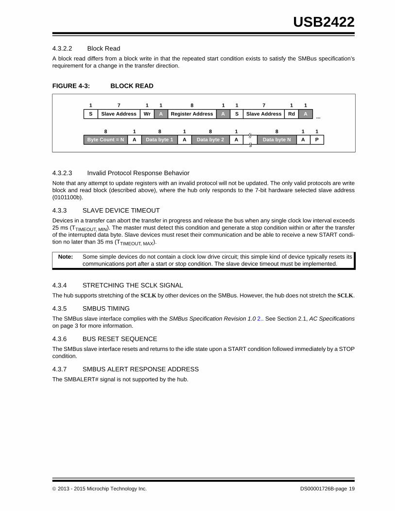
4.3.2.2 Block Read
A block read differs from a block write in that the repeated start condition exists to satisfy the SMBus specification’srequirement for a change in the transfer direction.
4.3.2.3 Invalid Protocol Response Behavior
Note that any attempt to update registers with an invalid protocol will not be updated. The only valid protocols are writeblock and read block (described above), where the hub only responds to the 7-bit hardware selected slave address(0101100b).
4.3.3 SLAVE DEVICE TIMEOUT
Devices in a transfer can abort the transfer in progress and release the bus when any single clock low interval exceeds25 ms (TTIMEOUT, MIN). The master must detect this condition and generate a stop condition within or after the transferof the interrupted data byte. Slave devices must reset their communication and be able to receive a new START condi-tion no later than 35 ms (TTIMEOUT, MAX).
4.3.4 STRETCHING THE SCLK SIGNAL
The hub supports stretching of the SCLK by other devices on the SMBus. However, the hub does not stretch the SCLK.
4.3.5 SMBUS TIMING
The SMBus slave interface complies with the SMBus Specification Revision 1.0 2.. See Section 2.1, AC Specificationson page 3 for more information.
4.3.6 BUS RESET SEQUENCE
The SMBus slave interface resets and returns to the idle state upon a START condition followed immediately by a STOPcondition.
4.3.7 SMBUS ALERT RESPONSE ADDRESS
The SMBALERT# signal is not supported by the hub.
FIGURE 4-3: BLOCK READ
Note: Some simple devices do not contain a clock low drive circuit; this simple kind of device typically resets itscommunications port after a start or stop condition. The slave device timeout must be implemented.
1
SS Slave Address Register AddressWr
1 7 1 1 8
A
1
Slave Address Rd A
7 1 1
...A
8 1 1 18 8 18 1
PA AAAByte Count = N Data byte 2Data byte 1 Data byte N
2013 - 2015 Microchip Technology Inc. DS00001726B-page 19
USB2422
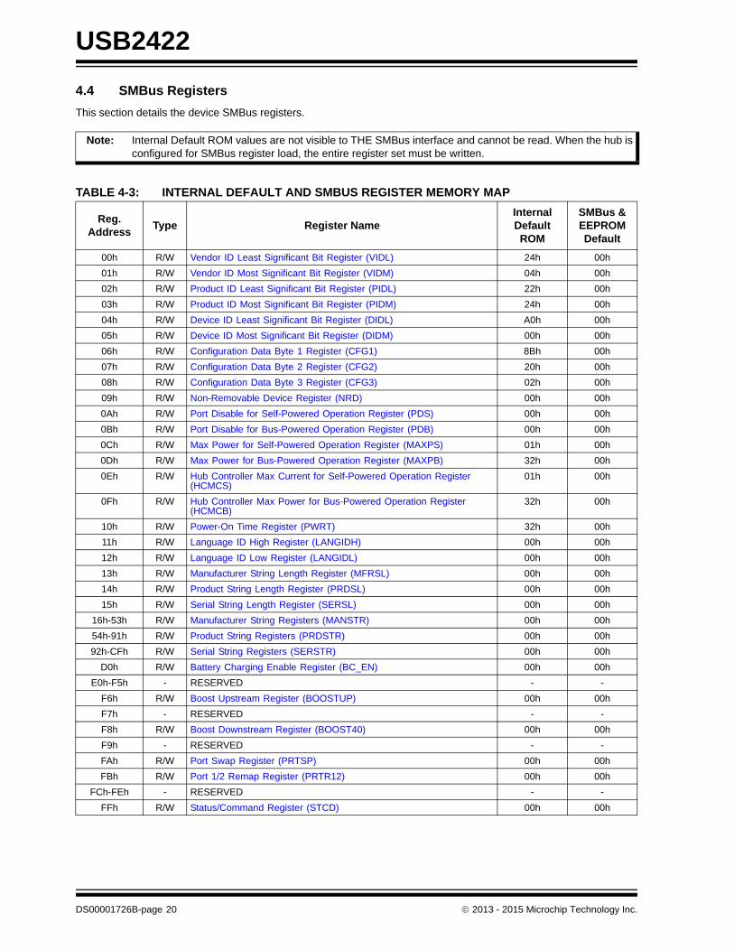
4.4 SMBus Registers
This section details the device SMBus registers.
Note: Internal Default ROM values are not visible to THE SMBus interface and cannot be read. When the hub isconfigured for SMBus register load, the entire register set must be written.
TABLE 4-3: INTERNAL DEFAULT AND SMBUS REGISTER MEMORY MAP
Reg. Address
Type Register NameInternal Default ROM
SMBus & EEPROM Default
00h R/W Vendor ID Least Significant Bit Register (VIDL) 24h 00h
01h R/W Vendor ID Most Significant Bit Register (VIDM) 04h 00h
02h R/W Product ID Least Significant Bit Register (PIDL) 22h 00h
03h R/W Product ID Most Significant Bit Register (PIDM) 24h 00h
04h R/W Device ID Least Significant Bit Register (DIDL) A0h 00h
05h R/W Device ID Most Significant Bit Register (DIDM) 00h 00h
06h R/W Configuration Data Byte 1 Register (CFG1) 8Bh 00h
07h R/W Configuration Data Byte 2 Register (CFG2) 20h 00h
08h R/W Configuration Data Byte 3 Register (CFG3) 02h 00h
09h R/W Non-Removable Device Register (NRD) 00h 00h
0Ah R/W Port Disable for Self-Powered Operation Register (PDS) 00h 00h
0Bh R/W Port Disable for Bus-Powered Operation Register (PDB) 00h 00h
0Ch R/W Max Power for Self-Powered Operation Register (MAXPS) 01h 00h
0Dh R/W Max Power for Bus-Powered Operation Register (MAXPB) 32h 00h
0Eh R/W Hub Controller Max Current for Self-Powered Operation Register (HCMCS)
01h 00h
0Fh R/W Hub Controller Max Power for Bus-Powered Operation Register (HCMCB)
32h 00h
10h R/W Power-On Time Register (PWRT) 32h 00h
11h R/W Language ID High Register (LANGIDH) 00h 00h
12h R/W Language ID Low Register (LANGIDL) 00h 00h
13h R/W Manufacturer String Length Register (MFRSL) 00h 00h
14h R/W Product String Length Register (PRDSL) 00h 00h
15h R/W Serial String Length Register (SERSL) 00h 00h
16h-53h R/W Manufacturer String Registers (MANSTR) 00h 00h
54h-91h R/W Product String Registers (PRDSTR) 00h 00h
92h-CFh R/W Serial String Registers (SERSTR) 00h 00h
D0h R/W Battery Charging Enable Register (BC_EN) 00h 00h
E0h-F5h - RESERVED - -
F6h R/W Boost Upstream Register (BOOSTUP) 00h 00h
F7h - RESERVED - -
F8h R/W Boost Downstream Register (BOOST40) 00h 00h
F9h - RESERVED - -
FAh R/W Port Swap Register (PRTSP) 00h 00h
FBh R/W Port 1/2 Remap Register (PRTR12) 00h 00h
FCh-FEh - RESERVED - -
FFh R/W Status/Command Register (STCD) 00h 00h
DS00001726B-page 20 2013 - 2015 Microchip Technology Inc.
USB2422
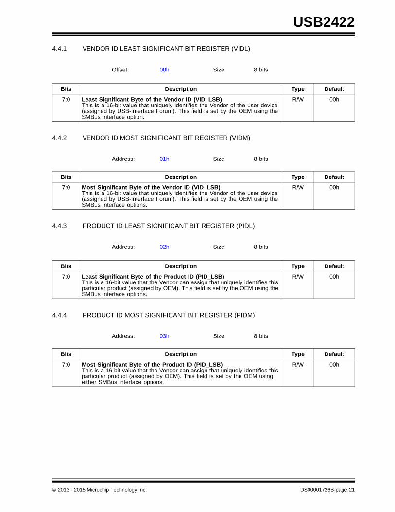
4.4.1 VENDOR ID LEAST SIGNIFICANT BIT REGISTER (VIDL)
4.4.2 VENDOR ID MOST SIGNIFICANT BIT REGISTER (VIDM)
4.4.3 PRODUCT ID LEAST SIGNIFICANT BIT REGISTER (PIDL)
4.4.4 PRODUCT ID MOST SIGNIFICANT BIT REGISTER (PIDM)
Offset: 00h Size: 8 bits
Bits Description Type Default
7:0 Least Significant Byte of the Vendor ID (VID_LSB)This is a 16-bit value that uniquely identifies the Vendor of the user device (assigned by USB-Interface Forum). This field is set by the OEM using the SMBus interface option.
R/W 00h
Address: 01h Size: 8 bits
Bits Description Type Default
7:0 Most Significant Byte of the Vendor ID (VID_LSB)This is a 16-bit value that uniquely identifies the Vendor of the user device (assigned by USB-Interface Forum). This field is set by the OEM using the SMBus interface options.
R/W 00h
Address: 02h Size: 8 bits
Bits Description Type Default
7:0 Least Significant Byte of the Product ID (PID_LSB)This is a 16-bit value that the Vendor can assign that uniquely identifies this particular product (assigned by OEM). This field is set by the OEM using the SMBus interface options.
R/W 00h
Address: 03h Size: 8 bits
Bits Description Type Default
7:0 Most Significant Byte of the Product ID (PID_LSB)This is a 16-bit value that the Vendor can assign that uniquely identifies this particular product (assigned by OEM). This field is set by the OEM using either SMBus interface options.
R/W 00h
2013 - 2015 Microchip Technology Inc. DS00001726B-page 21
USB2422
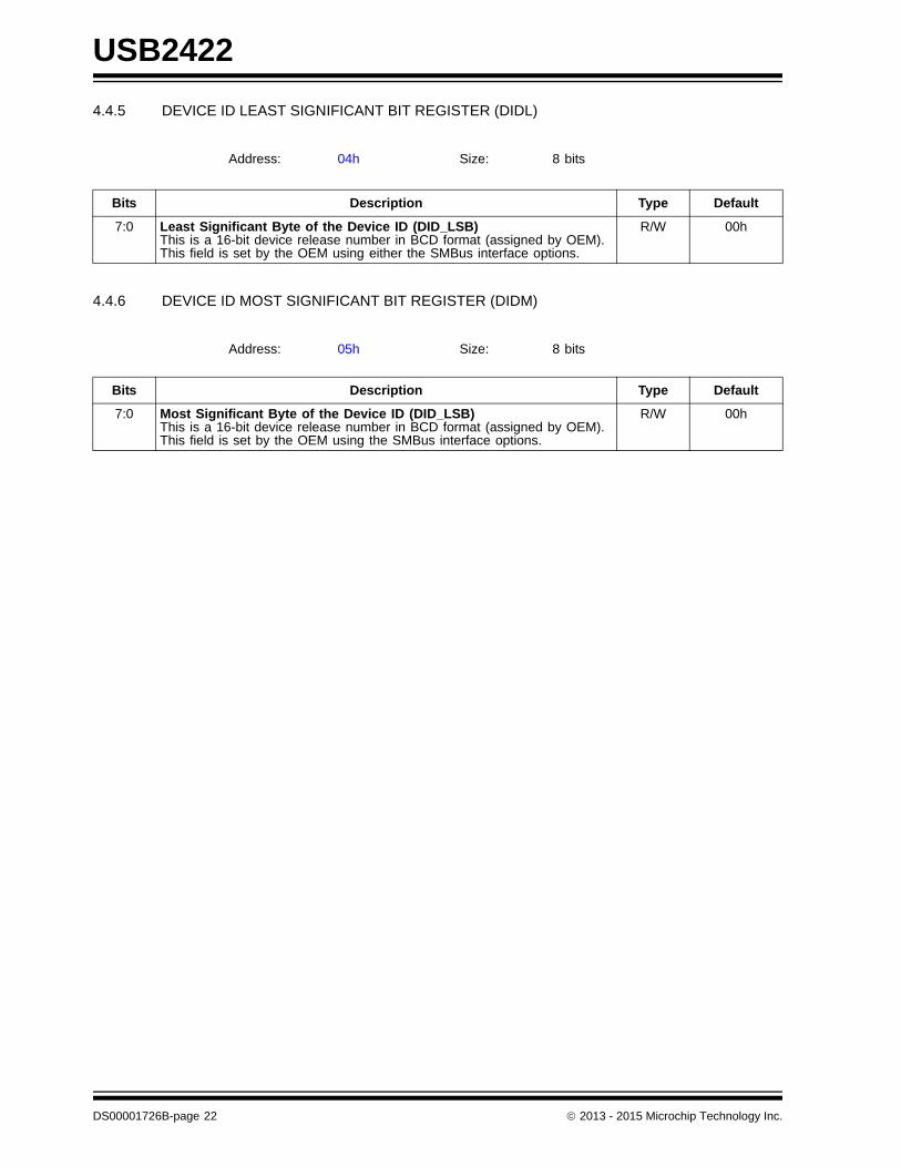
4.4.5 DEVICE ID LEAST SIGNIFICANT BIT REGISTER (DIDL)
4.4.6 DEVICE ID MOST SIGNIFICANT BIT REGISTER (DIDM)
Address: 04h Size: 8 bits
Bits Description Type Default
7:0 Least Significant Byte of the Device ID (DID_LSB)This is a 16-bit device release number in BCD format (assigned by OEM). This field is set by the OEM using either the SMBus interface options.
R/W 00h
Address: 05h Size: 8 bits
Bits Description Type Default
7:0 Most Significant Byte of the Device ID (DID_LSB)This is a 16-bit device release number in BCD format (assigned by OEM). This field is set by the OEM using the SMBus interface options.
R/W 00h
DS00001726B-page 22 2013 - 2015 Microchip Technology Inc.
USB2422
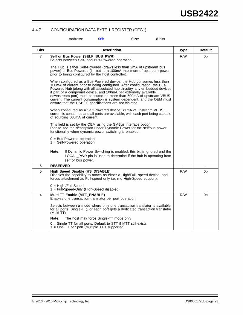
4.4.7 CONFIGURATION DATA BYTE 1 REGISTER (CFG1)
Address: 06h Size: 8 bits
Bits Description Type Default
7 Self or Bus Power (SELF_BUS_PWR)Selects between Self- and Bus-Powered operation.
The Hub is either Self-Powered (draws less than 2mA of upstream bus power) or Bus-Powered (limited to a 100mA maximum of upstream power prior to being configured by the host controller).
When configured as a Bus-Powered device, the Hub consumes less than 100mA of current prior to being configured. After configuration, the Bus-Powered Hub (along with all associated hub circuitry, any embedded devices if part of a compound device, and 100mA per externally available downstream port) must consume no more than 500mA of upstream VBUS current. The current consumption is system dependent, and the OEM must ensure that the USB2.0 specifications are not violated.
When configured as a Self-Powered device, <1mA of upstream VBUS current is consumed and all ports are available, with each port being capable of sourcing 500mA of current.
This field is set by the OEM using the SMBus interface option. Please see the description under Dynamic Power for the self/bus power functionality when dynamic power switching is enabled.
0 = Bus-Powered operation1 = Self-Powered operation
Note: If Dynamic Power Switching is enabled, this bit is ignored and the LOCAL_PWR pin is used to determine if the hub is operating from self or bus power.
R/W 0b
6 RESERVED - -
5 High Speed Disable (HS_DISABLE)Disables the capability to attach as either a High/Full- speed device, and forces attachment as Full-speed only i.e. (no High-Speed support).
0 = High-/Full-Speed1 = Full-Speed-Only (High-Speed disabled)
R/W 0b
4 Multi-TT Enable (MTT_ENABLE)Enables one transaction translator per port operation.
Selects between a mode where only one transaction translator is available for all ports (Single-TT), or each port gets a dedicated transaction translator (Multi-TT)
Note: The host may force Single-TT mode only
0 = Single TT for all ports. Default to STT if MTT still exists1 = One TT per port (multiple TT’s supported)
R/W 0b
2013 - 2015 Microchip Technology Inc. DS00001726B-page 23
USB2422
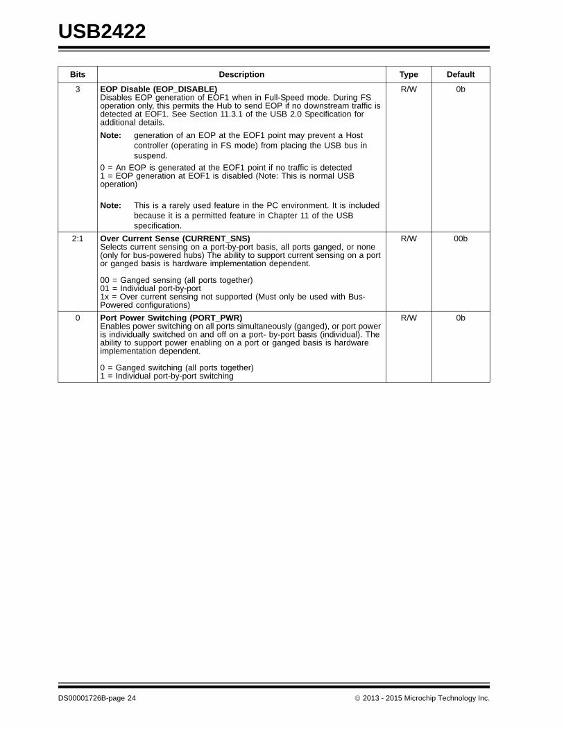
3 EOP Disable (EOP_DISABLE)Disables EOP generation of EOF1 when in Full-Speed mode. During FS operation only, this permits the Hub to send EOP if no downstream traffic is detected at EOF1. See Section 11.3.1 of the USB 2.0 Specification for additional details.
Note: generation of an EOP at the EOF1 point may prevent a Host controller (operating in FS mode) from placing the USB bus in suspend.
0 = An EOP is generated at the EOF1 point if no traffic is detected1 = EOP generation at EOF1 is disabled (Note: This is normal USB operation)
Note: This is a rarely used feature in the PC environment. It is included because it is a permitted feature in Chapter 11 of the USB specification.
R/W 0b
2:1 Over Current Sense (CURRENT_SNS)Selects current sensing on a port-by-port basis, all ports ganged, or none (only for bus-powered hubs) The ability to support current sensing on a port or ganged basis is hardware implementation dependent.
00 = Ganged sensing (all ports together)01 = Individual port-by-port1x = Over current sensing not supported (Must only be used with Bus- Powered configurations)
R/W 00b
0 Port Power Switching (PORT_PWR)Enables power switching on all ports simultaneously (ganged), or port power is individually switched on and off on a port- by-port basis (individual). The ability to support power enabling on a port or ganged basis is hardware implementation dependent.
0 = Ganged switching (all ports together)1 = Individual port-by-port switching
R/W 0b
Bits Description Type Default
DS00001726B-page 24 2013 - 2015 Microchip Technology Inc.
USB2422
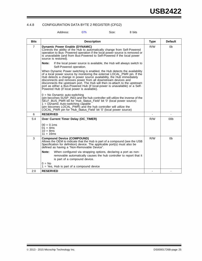
4.4.8 CONFIGURATION DATA BYTE 2 REGISTER (CFG2)
Address: 07h Size: 8 bits
Bits Description Type Default
7 Dynamic Power Enable (DYNAMIC)Controls the ability of the Hub to automatically change from Self-Powered operation to Bus- Powered operation if the local power source is removed or is unavailable (and from Bus-Powered to Self-Powered if the local power source is restored).
Note: If the local power source is available, the Hub will always switch to Self-Powered operation.
When Dynamic Power switching is enabled, the Hub detects the availability of a local power source by monitoring the external LOCAL_PWR pin. If the Hub detects a change in power source availability, the Hub immediately disconnects and removes power from all downstream devices and disconnects the upstream port. The Hub will then re-attach to the upstream port as either a Bus-Powered Hub (if local-power is unavailable) or a Self-Powered Hub (if local power is available).
0 = No Dynamic auto-switching(pin becomes SUSP_IND) and the hub controller will utilize the inverse of the SELF_BUS_PWR bit for 'Hub_Status_Field' bit '0' (local power source)1 = Dynamic Auto-switching capable(pin becomes LOCAL_PWR) and the hub controller will utilize the LOCAL_PWR pin for 'Hub_Status_Field' bit '0' (local power source)
R/W 0b
6 RESERVED - -
5:4 Over Current Timer Delay (OC_TIMER)
00 = 0.1ms01 = 4ms10 = 8ms11 = 16ms
R/W 00b
3 Compound Device (COMPOUND)Allows the OEM to indicate that the Hub is part of a compound (see the USB Specification for definition) device. The applicable port(s) must also be defined as having a “Non-Removable Device”.
Note: When configured via strapping options, declaring a port as non-removable automatically causes the hub controller to report that it is part of a compound device.
0 = No1 = Yes, Hub is part of a compound device
R/W 0b
2:0 RESERVED - -
2013 - 2015 Microchip Technology Inc. DS00001726B-page 25
USB2422
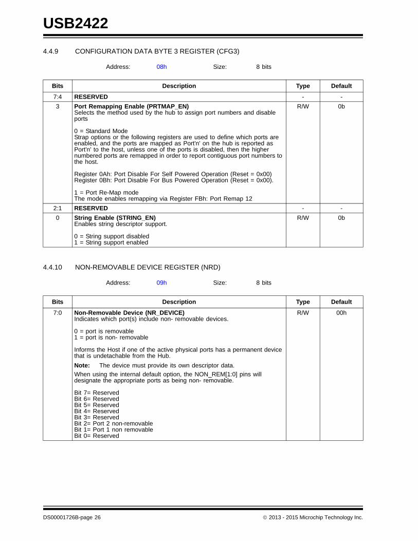
4.4.9 CONFIGURATION DATA BYTE 3 REGISTER (CFG3)
4.4.10 NON-REMOVABLE DEVICE REGISTER (NRD)
Address: 08h Size: 8 bits
Bits Description Type Default
7:4 RESERVED - -
3 Port Remapping Enable (PRTMAP_EN)Selects the method used by the hub to assign port numbers and disable ports
0 = Standard ModeStrap options or the following registers are used to define which ports are enabled, and the ports are mapped as Port'n' on the hub is reported as Port'n' to the host, unless one of the ports is disabled, then the higher numbered ports are remapped in order to report contiguous port numbers to the host.
Register 0Ah: Port Disable For Self Powered Operation (Reset = 0x00)Register 0Bh: Port Disable For Bus Powered Operation (Reset = 0x00).
1 = Port Re-Map modeThe mode enables remapping via Register FBh: Port Remap 12
R/W 0b
2:1 RESERVED - -
0 String Enable (STRING_EN)Enables string descriptor support.
0 = String support disabled1 = String support enabled
R/W 0b
Address: 09h Size: 8 bits
Bits Description Type Default
7:0 Non-Removable Device (NR_DEVICE)Indicates which port(s) include non- removable devices.
0 = port is removable1 = port is non- removable
Informs the Host if one of the active physical ports has a permanent device that is undetachable from the Hub.
Note: The device must provide its own descriptor data.
When using the internal default option, the NON_REM[1:0] pins will designate the appropriate ports as being non- removable.
Bit 7= ReservedBit 6= ReservedBit 5= ReservedBit 4= ReservedBit 3= ReservedBit 2= Port 2 non-removableBit 1= Port 1 non removableBit 0= Reserved
R/W 00h
DS00001726B-page 26 2013 - 2015 Microchip Technology Inc.
USB2422
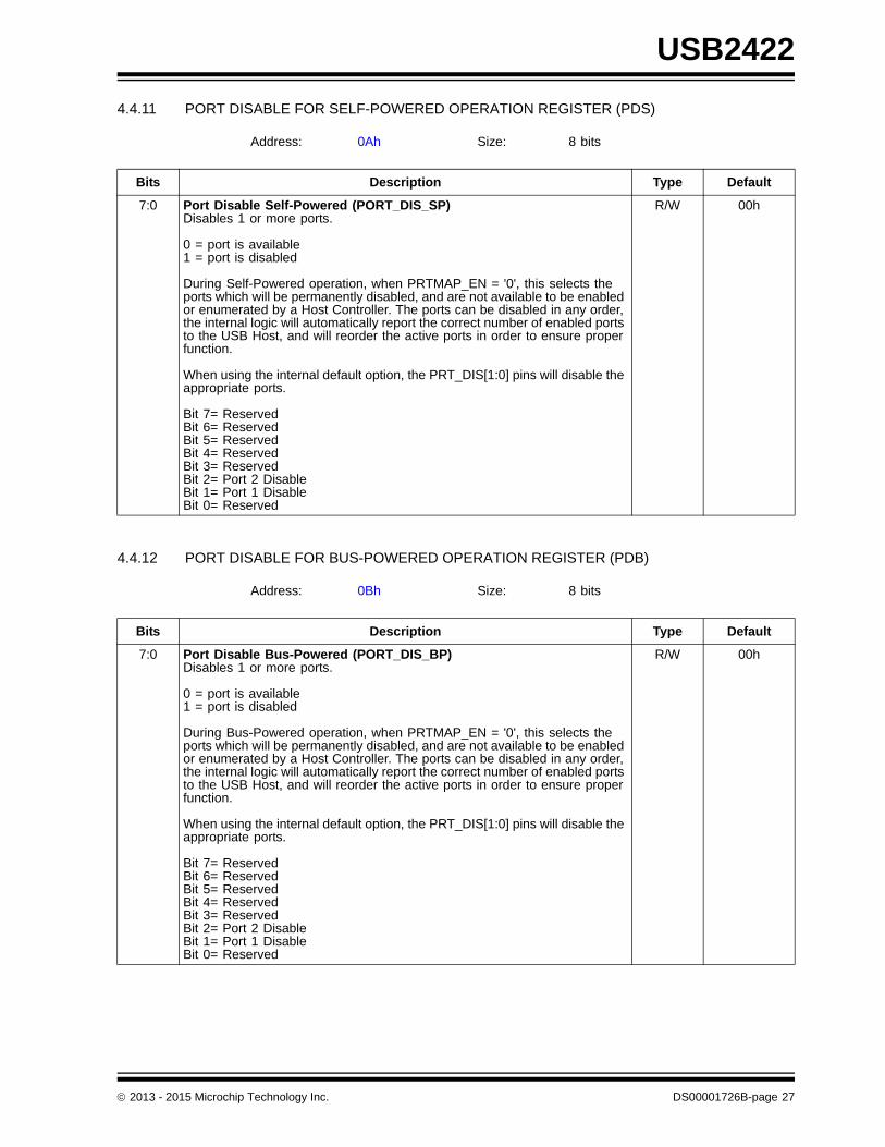
4.4.11 PORT DISABLE FOR SELF-POWERED OPERATION REGISTER (PDS)
4.4.12 PORT DISABLE FOR BUS-POWERED OPERATION REGISTER (PDB)
Address: 0Ah Size: 8 bits
Bits Description Type Default
7:0 Port Disable Self-Powered (PORT_DIS_SP)Disables 1 or more ports.
0 = port is available1 = port is disabled
During Self-Powered operation, when PRTMAP_EN = '0', this selects the ports which will be permanently disabled, and are not available to be enabled or enumerated by a Host Controller. The ports can be disabled in any order, the internal logic will automatically report the correct number of enabled ports to the USB Host, and will reorder the active ports in order to ensure proper function.
When using the internal default option, the PRT_DIS[1:0] pins will disable the appropriate ports.
Bit 7= ReservedBit 6= ReservedBit 5= ReservedBit 4= ReservedBit 3= ReservedBit 2= Port 2 DisableBit 1= Port 1 DisableBit 0= Reserved
R/W 00h
Address: 0Bh Size: 8 bits
Bits Description Type Default
7:0 Port Disable Bus-Powered (PORT_DIS_BP)Disables 1 or more ports.
0 = port is available1 = port is disabled
During Bus-Powered operation, when PRTMAP_EN = '0', this selects the ports which will be permanently disabled, and are not available to be enabled or enumerated by a Host Controller. The ports can be disabled in any order, the internal logic will automatically report the correct number of enabled ports to the USB Host, and will reorder the active ports in order to ensure proper function.
When using the internal default option, the PRT_DIS[1:0] pins will disable the appropriate ports.
Bit 7= ReservedBit 6= ReservedBit 5= ReservedBit 4= ReservedBit 3= ReservedBit 2= Port 2 DisableBit 1= Port 1 DisableBit 0= Reserved
R/W 00h
2013 - 2015 Microchip Technology Inc. DS00001726B-page 27
USB2422
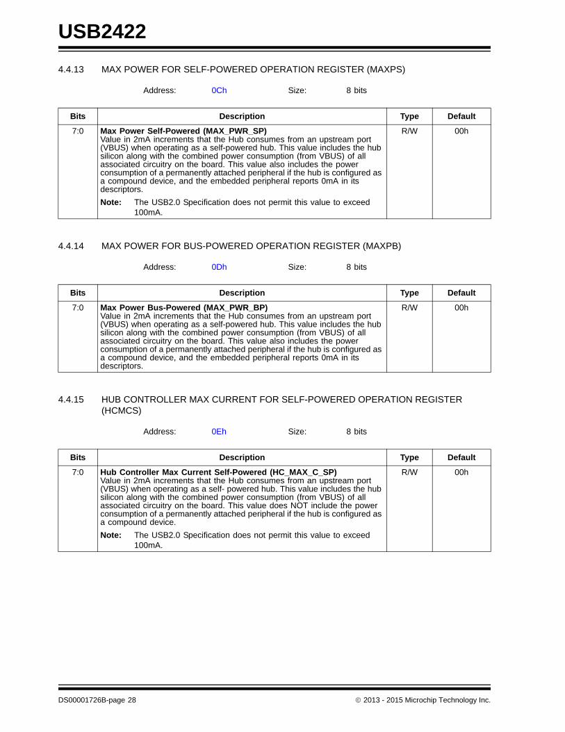
4.4.13 MAX POWER FOR SELF-POWERED OPERATION REGISTER (MAXPS)
4.4.14 MAX POWER FOR BUS-POWERED OPERATION REGISTER (MAXPB)
4.4.15 HUB CONTROLLER MAX CURRENT FOR SELF-POWERED OPERATION REGISTER (HCMCS)
Address: 0Ch Size: 8 bits
Bits Description Type Default
7:0 Max Power Self-Powered (MAX_PWR_SP)Value in 2mA increments that the Hub consumes from an upstream port (VBUS) when operating as a self-powered hub. This value includes the hub silicon along with the combined power consumption (from VBUS) of all associated circuitry on the board. This value also includes the power consumption of a permanently attached peripheral if the hub is configured as a compound device, and the embedded peripheral reports 0mA in its descriptors.
Note: The USB2.0 Specification does not permit this value to exceed 100mA.
R/W 00h
Address: 0Dh Size: 8 bits
Bits Description Type Default
7:0 Max Power Bus-Powered (MAX_PWR_BP)Value in 2mA increments that the Hub consumes from an upstream port (VBUS) when operating as a self-powered hub. This value includes the hub silicon along with the combined power consumption (from VBUS) of all associated circuitry on the board. This value also includes the power consumption of a permanently attached peripheral if the hub is configured as a compound device, and the embedded peripheral reports 0mA in its descriptors.
R/W 00h
Address: 0Eh Size: 8 bits
Bits Description Type Default
7:0 Hub Controller Max Current Self-Powered (HC_MAX_C_SP)Value in 2mA increments that the Hub consumes from an upstream port (VBUS) when operating as a self- powered hub. This value includes the hub silicon along with the combined power consumption (from VBUS) of all associated circuitry on the board. This value does NOT include the power consumption of a permanently attached peripheral if the hub is configured as a compound device.
Note: The USB2.0 Specification does not permit this value to exceed 100mA.
R/W 00h
DS00001726B-page 28 2013 - 2015 Microchip Technology Inc.
USB2422
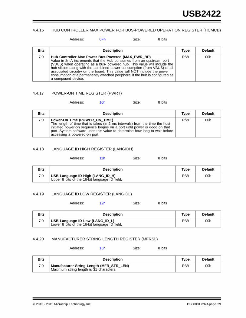
4.4.16 HUB CONTROLLER MAX POWER FOR BUS-POWERED OPERATION REGISTER (HCMCB)
4.4.17 POWER-ON TIME REGISTER (PWRT)
4.4.18 LANGUAGE ID HIGH REGISTER (LANGIDH)
4.4.19 LANGUAGE ID LOW REGISTER (LANGIDL)
4.4.20 MANUFACTURER STRING LENGTH REGISTER (MFRSL)
Address: 0Fh Size: 8 bits
Bits Description Type Default
7:0 Hub Controller Max Power Bus-Powered (MAX_PWR_BP)Value in 2mA increments that the Hub consumes from an upstream port (VBUS) when operating as a bus- powered hub. This value will include the hub silicon along with the combined power consumption (from VBUS) of all associated circuitry on the board. This value will NOT include the power consumption of a permanently attached peripheral if the hub is configured as a compound device.
R/W 00h
Address: 10h Size: 8 bits
Bits Description Type Default
7:0 Power-On Time (POWER_ON_TIME)The length of time that is takes (in 2 ms intervals) from the time the host initiated power-on sequence begins on a port until power is good on that port. System software uses this value to determine how long to wait before accessing a powered-on port.
R/W 00h
Address: 11h Size: 8 bits
Bits Description Type Default
7:0 USB Language ID High (LANG_ID_H)Upper 8 bits of the 16-bit language ID field.
R/W 00h
Address: 12h Size: 8 bits
Bits Description Type Default
7:0 USB Language ID Low (LANG_ID_L)Lower 8 bits of the 16-bit language ID field.
R/W 00h
Address: 13h Size: 8 bits
Bits Description Type Default
7:0 Manufacturer String Length (MFR_STR_LEN)Maximum string length is 31 characters.
R/W 00h
2013 - 2015 Microchip Technology Inc. DS00001726B-page 29
USB2422
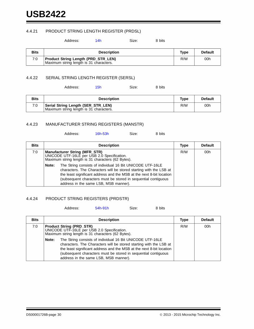
4.4.21 PRODUCT STRING LENGTH REGISTER (PRDSL)
4.4.22 SERIAL STRING LENGTH REGISTER (SERSL)
4.4.23 MANUFACTURER STRING REGISTERS (MANSTR)
4.4.24 PRODUCT STRING REGISTERS (PRDSTR)
Address: 14h Size: 8 bits
Bits Description Type Default
7:0 Product String Length (PRD_STR_LEN)Maximum string length is 31 characters.
R/W 00h
Address: 15h Size: 8 bits
Bits Description Type Default
7:0 Serial String Length (SER_STR_LEN)Maximum string length is 31 characters.
R/W 00h
Address: 16h-53h Size: 8 bits
Bits Description Type Default
7:0 Manufacturer String (MFR_STR)UNICODE UTF-16LE per USB 2.0 Specification.Maximum string length is 31 characters (62 Bytes).
Note: The String consists of individual 16 Bit UNICODE UTF-16LE characters. The Characters will be stored starting with the LSB at the least significant address and the MSB at the next 8-bit location (subsequent characters must be stored in sequential contiguous address in the same LSB, MSB manner).
R/W 00h
Address: 54h-91h Size: 8 bits
Bits Description Type Default
7:0 Product String (PRD_STR)UNICODE UTF-16LE per USB 2.0 Specification.Maximum string length is 31 characters (62 Bytes).
Note: The String consists of individual 16 Bit UNICODE UTF-16LE characters. The Characters will be stored starting with the LSB at the least significant address and the MSB at the next 8-bit location (subsequent characters must be stored in sequential contiguous address in the same LSB, MSB manner).
R/W 00h
DS00001726B-page 30 2013 - 2015 Microchip Technology Inc.
USB2422
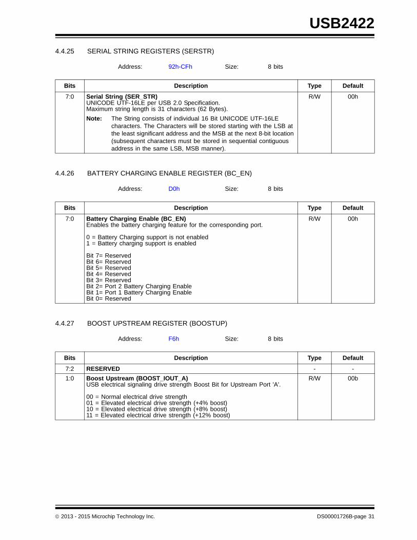
4.4.25 SERIAL STRING REGISTERS (SERSTR)
4.4.26 BATTERY CHARGING ENABLE REGISTER (BC_EN)
4.4.27 BOOST UPSTREAM REGISTER (BOOSTUP)
Address: 92h-CFh Size: 8 bits
Bits Description Type Default
7:0 Serial String (SER_STR)UNICODE UTF-16LE per USB 2.0 Specification.Maximum string length is 31 characters (62 Bytes).
Note: The String consists of individual 16 Bit UNICODE UTF-16LE characters. The Characters will be stored starting with the LSB at the least significant address and the MSB at the next 8-bit location (subsequent characters must be stored in sequential contiguous address in the same LSB, MSB manner).
R/W 00h
Address: D0h Size: 8 bits
Bits Description Type Default
7:0 Battery Charging Enable (BC_EN)Enables the battery charging feature for the corresponding port.
0 = Battery Charging support is not enabled1 = Battery charging support is enabled
Bit 7= ReservedBit 6= ReservedBit 5= ReservedBit 4= ReservedBit 3= ReservedBit 2= Port 2 Battery Charging EnableBit 1= Port 1 Battery Charging EnableBit 0= Reserved
R/W 00h
Address: F6h Size: 8 bits
Bits Description Type Default
7:2 RESERVED - -
1:0 Boost Upstream (BOOST_IOUT_A)USB electrical signaling drive strength Boost Bit for Upstream Port 'A'.
00 = Normal electrical drive strength01 = Elevated electrical drive strength (+4% boost)10 = Elevated electrical drive strength (+8% boost)11 = Elevated electrical drive strength (+12% boost)
R/W 00b
2013 - 2015 Microchip Technology Inc. DS00001726B-page 31

USB2422
4.4.28 BOOST DOWNSTREAM REGISTER (BOOST40)
4.4.29 PORT SWAP REGISTER (PRTSP)
Address: F8h Size: 8 bits
Bits Description Type Default
7:4 RESERVED - -
3:2 Boost Downstream Port 2 (BOOST_IOUT_2)USB electrical signaling drive strength Boost Bit for Upstream Port '2'.
00 = Normal electrical drive strength01 = Elevated electrical drive strength (+4% boost)10 = Elevated electrical drive strength (+8% boost)11 = Elevated electrical drive strength (+12% boost)
R/W 00b
1:0 Boost Downstream Port 1 (BOOST_IOUT_1)USB electrical signaling drive strength Boost Bit for Upstream Port '1'.
00 = Normal electrical drive strength01 = Elevated electrical drive strength (+4% boost)10 = Elevated electrical drive strength (+8% boost)11 = Elevated electrical drive strength (+12% boost)
R/W 00b
Address: FAh Size: 8 bits
Bits Description Type Default
7:0 Port Swap (PRTSP)Swaps the Upstream and Downstream USB DP and DM Pins for ease of board routing to devices and connectors.
0 = USB D+ functionality is associated with the DP pin and D- functionality is associated with the DM pin.1 = USB D+ functionality is associated with the DM pin and D- functionality is associated with the DP pin
Bit 7= ReservedBit 6= ReservedBit 5= ReservedBit 4= ReservedBit 3= ReservedBit 2= Port 2 DP/DM SwapBit 1= Port 1 DP/DM SwapBit 0= Upstream Port DP/DM Swap
R/W 00h
DS00001726B-page 32 2013 - 2015 Microchip Technology Inc.
USB2422
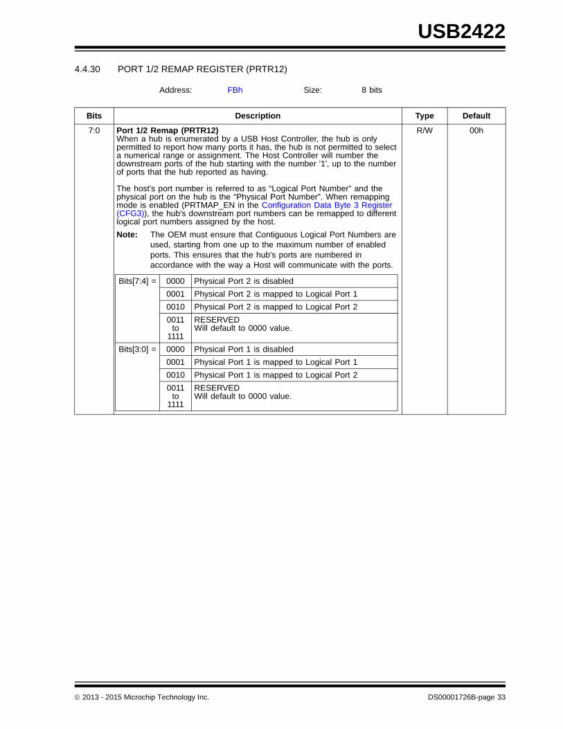
4.4.30 PORT 1/2 REMAP REGISTER (PRTR12)
Address: FBh Size: 8 bits
Bits Description Type Default
7:0 Port 1/2 Remap (PRTR12)When a hub is enumerated by a USB Host Controller, the hub is only permitted to report how many ports it has, the hub is not permitted to select a numerical range or assignment. The Host Controller will number the downstream ports of the hub starting with the number '1', up to the number of ports that the hub reported as having.
The host's port number is referred to as “Logical Port Number” and the physical port on the hub is the “Physical Port Number”. When remapping mode is enabled (PRTMAP_EN in the Configuration Data Byte 3 Register (CFG3)), the hub's downstream port numbers can be remapped to different logical port numbers assigned by the host.
Note: The OEM must ensure that Contiguous Logical Port Numbers are used, starting from one up to the maximum number of enabled ports. This ensures that the hub's ports are numbered in accordance with the way a Host will communicate with the ports.
R/W 00h
Bits[7:4] = 0000 Physical Port 2 is disabled
0001 Physical Port 2 is mapped to Logical Port 1
0010 Physical Port 2 is mapped to Logical Port 2
0011to
1111
RESERVEDWill default to 0000 value.
Bits[3:0] = 0000 Physical Port 1 is disabled
0001 Physical Port 1 is mapped to Logical Port 1
0010 Physical Port 1 is mapped to Logical Port 2
0011to
1111
RESERVEDWill default to 0000 value.
2013 - 2015 Microchip Technology Inc. DS00001726B-page 33
USB2422
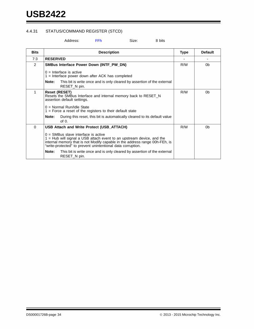
4.4.31 STATUS/COMMAND REGISTER (STCD)
Address: FFh Size: 8 bits
Bits Description Type Default
7:3 RESERVED - -
2 SMBus Interface Power Down (INTF_PW_DN)
0 = Interface is active1 = Interface power down after ACK has completed
Note: This bit is write once and is only cleared by assertion of the external RESET_N pin.
R/W 0b
1 Reset (RESET)Resets the SMBus Interface and internal memory back to RESET_N assertion default settings.
0 = Normal Run/Idle State1 = Force a reset of the registers to their default state
Note: During this reset, this bit is automatically cleared to its default value of 0.
R/W 0b
0 USB Attach and Write Protect (USB_ATTACH)
0 = SMBus slave interface is active1 = Hub will signal a USB attach event to an upstream device, and the internal memory that is not Modify capable in the address range 00h-FEh, is “write-protected” to prevent unintentional data corruption.
Note: This bit is write once and is only cleared by assertion of the external RESET_N pin.
R/W 0b
DS00001726B-page 34 2013 - 2015 Microchip Technology Inc.

USB2422
5.0 DC PARAMETERS
5.1 Maximum Ratings
Note 5-1 Refer to JEDEC Specification J-STD-020D [3].
Note 5-2 Stresses above the specified parameters could cause permanent damage to the device. This is astress rating only and functional operation of the device at any condition above those indicated in theoperation sections of this specification is not implied.
Note 5-3 When powering this device from laboratory or system power supplies, it is important that the absolutemaximum ratings not be exceeded or device failure can result. Some power supplies exhibit voltagespikes on their outputs when the AC power is switched on or off. In addition, voltage transients onthe AC power line may appear on the DC output. When this possibility exists, it is suggested that aclamp circuit be used.
5.2 Operating Conditions
Parameter Symbol MIN MAX Units Comments
Storage Temperature TSTOR -55 150 °C
Lead Temperature Refer to JEDEC Specification J-STD-020D 3.
3.3 V supply voltage VDD33 4.6 V
Voltage on any I/O pin -0.5 5.5 V
Voltage on XTALIN -0.5 4.0 V
Voltage on XTALOUT -0.5 2.5 V
Parameter Symbol MIN MAX Units Comments
USB2422 Operating Temperature
TA 0 70 °C Ambient temperature in still air
USB2422-i Operating Temperature
TA -40 85 °C Ambient temperature in still air
3.3 V supply voltage VDD33 3.0 3.6 V
3.3 V supply rise time tRT33 0 400 μs See Figure 5-1
Voltage on any I/O pin -0.3 5.5 V If any 3.3 V supply voltage drops below 3.0 V, then the MAX becomes:
(3.3 V supply voltage) + 0.5
Voltage on XTALIN -0.3 VDD12 + 0.3
V
2013 - 2015 Microchip Technology Inc. DS00001726B-page 35

USB2422
FIGURE 5-1: SUPPLY RISE TIME MODEL
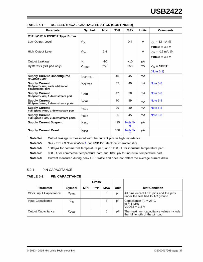
TABLE 5-1: DC ELECTRICAL CHARACTERISTICS
Parameter Symbol MIN TYP MAX Units Comments
I, IS Type Input Buffer
Low Input Level VILI 0.8 V TTL Levels
High Input Level VIHI 2.0 V
Input Leakage IIL -10 +10 μA VIN = 0 to VDD33
Hysteresis (IS only) VHYSI 250 350 mV
Input Buffer with Pull-Up (IPU)
Low Input Level VILI 0.8 V TTL Levels
High Input Level VIHI 2.0 V
Low Input Leakage IILL +35 +90 μA VIN = 0
High Input Leakage IIHL -10 +10 μA VIN = VDD33
Input Buffer with Pull-Down (IPD)
Low Input Level VILI 0.8 V TTL Levels
High Input Level VIHI 2.0 V
Low Input Leakage IILL +10 -10 μA VIN = 0
High Input Leakage IIHL -35 -90 μA VIN = VDD33
ICLK Input Buffer
Low Input Level VILCK 0.3 V
High Input Level VIHCK 0.9 V
Input Leakage IIL -10 +10 μA VIN = 0 to VDD33
t10%
10%
90%
Voltage tRT33
t90% Time
100%3.3 V
VSS
VDD33
DS00001726B-page 36 2013 - 2015 Microchip Technology Inc.
USB2422
Note 5-4 Output leakage is measured with the current pins in high impedance.
Note 5-5 See USB 2.0 Specification 1. for USB DC electrical characteristics.
Note 5-6 1000 μA for commercial temperature part, and 1200 μA for industrial temperature part.
Note 5-7 800 μA for commercial temperature part, and 1000 μA for industrial temperature part.
Note 5-8 Current measured during peak USB traffic and does not reflect the average current draw.
5.2.1 PIN CAPACITANCE
O12, I/O12 & I/OSD12 Type Buffer
Low Output Level VOL 0.4 V IOL = 12 mA @
VDD33 = 3.3 V
High Output Level VOH 2.4 V IOH = -12 mA @
VDD33 = 3.3 V
Output Leakage IOL -10 +10 μA
Hysteresis (SD pad only) VHYSC 250 350 mV VIN = VDD33
(Note 5-1)
Supply Current UnconfiguredHi-Speed Host
ICCINTHS 40 45 mA
Supply CurrentHi-Speed Host, each additional downstream port
ICCINTFS 35 40 mA Note 5-8
Supply CurrentHi-Speed Host, 1 downstream port
IHCH1 47 58 mA Note 5-8
Supply CurrentHi-Speed Host, 2 downstream ports
IHCH2 70 89 mA Note 5-8
Supply CurrentFull-Speed Host, 1 downstream port
IFCC1 29 40 mA Note 5-8
Supply CurrentFull-Speed Host, 2 downstream ports
IFCC2 35 45 mA Note 5-8
Supply Current Suspend ICSBY 425 Note 5-6
μA
Supply Current Reset ICRST 300 Note 5-7
μA
TABLE 5-2: PIN CAPACITANCE
Limits
Parameter Symbol MIN TYP MAX Unit Test Condition
Clock Input Capacitance CXTAL 6 pF All pins except USB pins and the pins under the test tied to AC ground.
Input Capacitance CIN 6 pF Capacitance TA = 25°Cfc = 1 MHzVDD33 = 3.3 V
Output Capacitance COUT 6 pF The maximum capacitance values include the full length of the pin pad.
TABLE 5-1: DC ELECTRICAL CHARACTERISTICS (CONTINUED)
Parameter Symbol MIN TYP MAX Units Comments
2013 - 2015 Microchip Technology Inc. DS00001726B-page 37
USB2422
6.0 AC SPECIFICATIONS
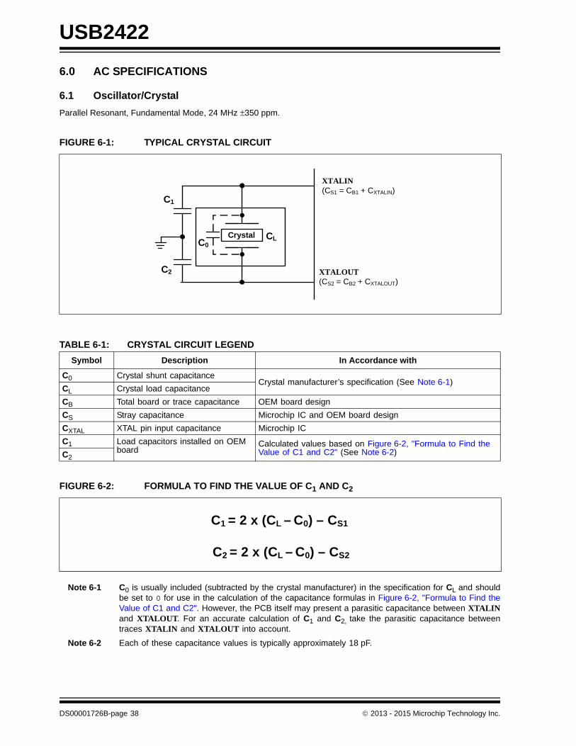
6.1 Oscillator/Crystal
Parallel Resonant, Fundamental Mode, 24 MHz ±350 ppm.
Note 6-1 C0 is usually included (subtracted by the crystal manufacturer) in the specification for CL and shouldbe set to 0 for use in the calculation of the capacitance formulas in Figure 6-2, "Formula to Find theValue of C1 and C2". However, the PCB itself may present a parasitic capacitance between XTALINand XTALOUT. For an accurate calculation of C1 and C2, take the parasitic capacitance betweentraces XTALIN and XTALOUT into account.
Note 6-2 Each of these capacitance values is typically approximately 18 pF.
FIGURE 6-1: TYPICAL CRYSTAL CIRCUIT
TABLE 6-1: CRYSTAL CIRCUIT LEGEND
Symbol Description In Accordance with
C0 Crystal shunt capacitanceCrystal manufacturer’s specification (See Note 6-1)
CL Crystal load capacitance
CB Total board or trace capacitance OEM board design
CS Stray capacitance Microchip IC and OEM board design
CXTAL XTAL pin input capacitance Microchip IC
C1 Load capacitors installed on OEM board
Calculated values based on Figure 6-2, "Formula to Find the Value of C1 and C2" (See Note 6-2)C2
FIGURE 6-2: FORMULA TO FIND THE VALUE OF C1 AND C2
C1
C2
CLCrystalC0
XTALIN(CS1 = CB1 + CXTALIN)
XTALOUT(CS2 = CB2 + CXTALOUT)
C1 = 2 x (CL – C0) – CS1
C2 = 2 x (CL – C0) – CS2
DS00001726B-page 38 2013 - 2015 Microchip Technology Inc.
USB2422
6.2 External Clock
50% Duty cycle ± 10%, 24 MHz ± 350 ppm.
The external clock is recommended to conform to the signaling level designated in the JESD76-2 specification on 1.2 VCMOS Logic. XTALOUT should be treated as a weak (< 1 mA) buffer output.
6.2.1 USB 2.0
The Microchip hub conforms to all voltage, power, and timing characteristics and specifications as set forth in the USB2.0 Specification 1.. See the USB Specification for more information.
6.3 SMBus Interface
The Microchip hub conforms to all voltage, power, and timing characteristics and specifications as set forth in the SMBus1.0 Specification 2. for slave-only devices (except as noted in Section 4.3, "SMBus," on page 18).
2013 - 2015 Microchip Technology Inc. DS00001726B-page 39

USB2422
DS00001726B-page 40 2013 - 2015 Microchip Technology Inc.
7.0 PACKAGE OUTLINE
FIGURE 7-1: 24-SQFN PACKAGE
Not
e: F
or th
e m
ost c
urre
nt p
acka
ge d
raw
ings
, se
e th
e M
icro
chip
Pac
kagi
ng S
peci
ficat
ion
at
http
://w
ww
.mic
roch
ip.c
om/p
acka
ging
2013 - 2015 Microchip Technology Inc. DS00001726B-page 41
USB2422
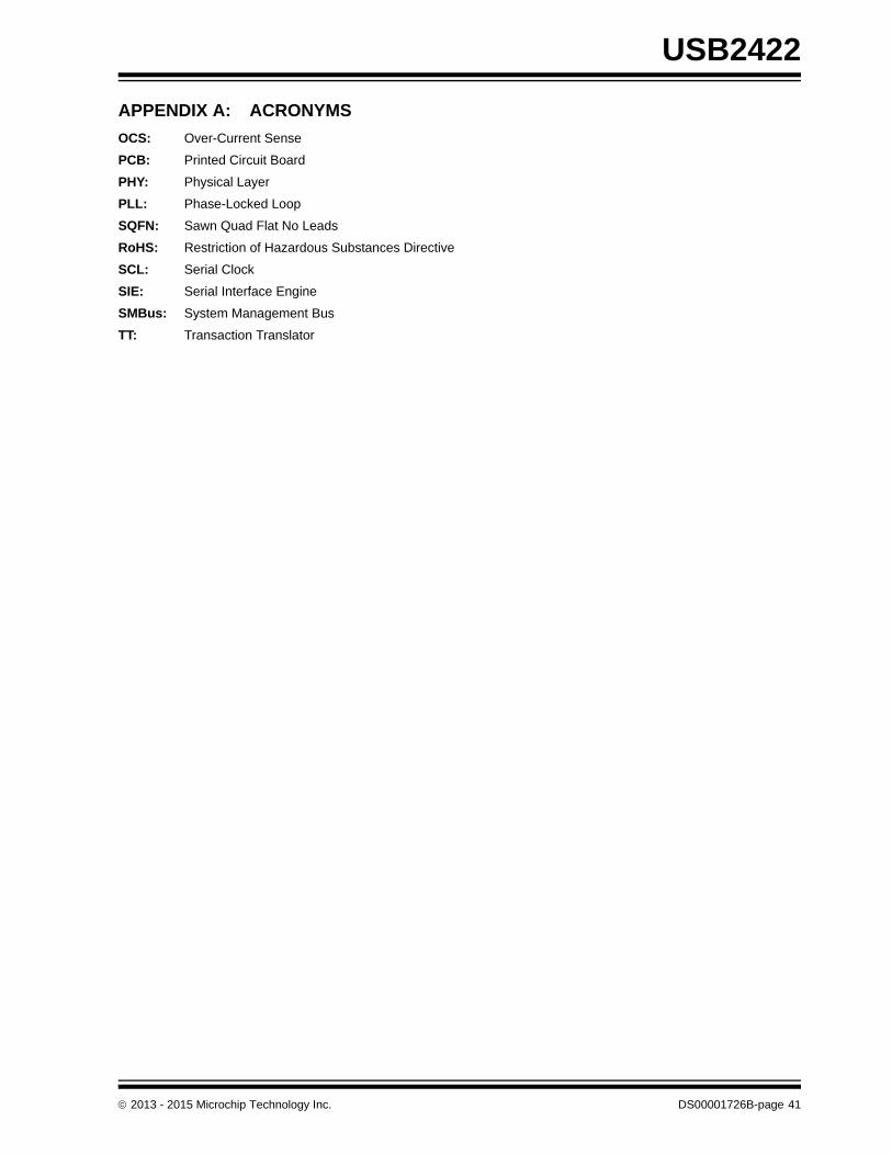
APPENDIX A: ACRONYMS
OCS: Over-Current Sense
PCB: Printed Circuit Board
PHY: Physical Layer
PLL: Phase-Locked Loop
SQFN: Sawn Quad Flat No Leads
RoHS: Restriction of Hazardous Substances Directive
SCL: Serial Clock
SIE: Serial Interface Engine
SMBus: System Management Bus
TT: Transaction Translator
USB2422
DS00001726B-page 42 2013 - 2015 Microchip Technology Inc.
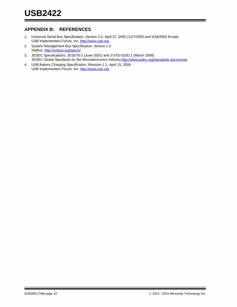
APPENDIX B: REFERENCES
1. Universal Serial Bus Specification, Version 2.0, April 27, 2000 (12/7/2000 and 5/28/2002 Errata)USB Implementers Forum, Inc. http://www.usb.org
2. System Management Bus Specification, version 1.0SMBus. http://smbus.org/specs/
3. JEDEC Specifications: JESD76-2 (June 2001) and J-STD-020D.1 (March 2008)JEDEC Global Standards for the Microelectronics Industry.http://www.jedec.org/standards-documents
4. USB Battery Charging Specification, Revision 1.1, April 15, 2009USB Implementers Forum, Inc. http://www.usb.org
2013 - 2015 Microchip Technology Inc. DS00001726B-page 43
USB2422
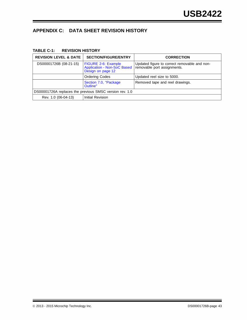
APPENDIX C: DATA SHEET REVISION HISTORY
TABLE C-1: REVISION HISTORY
REVISION LEVEL & DATE SECTION/FIGURE/ENTRY CORRECTION
DS00001726B (08-21-15) FIGURE 2-6: Example Application - Non-SoC Based Design on page 12
Updated figure to correct removable and non-removable port assignments.
Ordering Codes Updated reel size to 5000.
Section 7.0, "Package Outline"
Removed tape and reel drawings.
DS00001726A replaces the previous SMSC version rev. 1.0
Rev. 1.0 (06-04-13) Initial Revision
USB2422
DS00001726B-page 44 2013 - 2015 Microchip Technology Inc.
THE MICROCHIP WEB SITE
Microchip provides online support via our WWW site at www.microchip.com. This web site is used as a means to makefiles and information easily available to customers. Accessible by using your favorite Internet browser, the web site con-tains the following information:
• Product Support – Data sheets and errata, application notes and sample programs, design resources, user’s guides and hardware support documents, latest software releases and archived software
• General Technical Support – Frequently Asked Questions (FAQ), technical support requests, online discussion groups, Microchip consultant program member listing
• Business of Microchip – Product selector and ordering guides, latest Microchip press releases, listing of semi-nars and events, listings of Microchip sales offices, distributors and factory representatives
CUSTOMER CHANGE NOTIFICATION SERVICE
Microchip’s customer notification service helps keep customers current on Microchip products. Subscribers will receivee-mail notification whenever there are changes, updates, revisions or errata related to a specified product family ordevelopment tool of interest.
To register, access the Microchip web site at www.microchip.com. Under “Support”, click on “Customer Change Notifi-cation” and follow the registration instructions.
CUSTOMER SUPPORT
Users of Microchip products can receive assistance through several channels:
• Distributor or Representative
• Local Sales Office
• Field Application Engineer (FAE)
• Technical Support
Customers should contact their distributor, representative or field application engineer (FAE) for support. Local salesoffices are also available to help customers. A listing of sales offices and locations is included in the back of this docu-ment.
Technical support is available through the web site at: http://www.microchip.com/support
2013 - 2015 Microchip Technology Inc. DS00001726B-page 45
USB2422
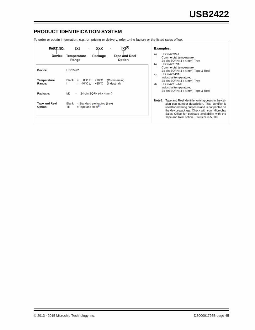
PRODUCT IDENTIFICATION SYSTEM
To order or obtain information, e.g., on pricing or delivery, refer to the factory or the listed sales office.
Device: USB2422
Temperature Range:
Blank = 0°C to +70°C (Commercial)I = -40°C to +85°C (Industrial)
Package: MJ = 24-pin SQFN (4 x 4 mm)
Tape and Reel Option:
Blank = Standard packaging (tray)TR = Tape and Reel (1)
Examples:
a) USB2422/MJCommercial temperature,24-pin SQFN (4 x 4 mm) Tray
b) USB2422T/MJCommercial temperature,24-pin SQFN (4 x 4 mm) Tape & Reel
c) USB2422-I/MJIndustrial temperature,24-pin SQFN (4 x 4 mm) Tray
d) USB2422T-I/MJIndustrial temperature,24-pin SQFN (4 x 4 mm) Tape & Reel
Note1: Tape and Reel identifier only appears in the cat-alog part number description. This identifier isused for ordering purposes and is not printed onthe device package. Check with your MicrochipSales Office for package availability with theTape and Reel option. Reel size is 5,000.
PART NO. [X] XXX
PackageTemperatureRange
Device
[X](1)
Tape and ReelOption
- -
USB2422
DS00001726B-page 46 2013 - 2015 Microchip Technology Inc.
Note the following details of the code protection feature on Microchip devices:
• Microchip products meet the specification contained in their particular Microchip Data Sheet.
• Microchip believes that its family of products is one of the most secure families of its kind on the market today, when used in the intended manner and under normal conditions.
• There are dishonest and possibly illegal methods used to breach the code protection feature. All of these methods, to our knowledge, require using the Microchip products in a manner outside the operating specifications contained in Microchip’s Data Sheets. Most likely, the person doing so is engaged in theft of intellectual property.
• Microchip is willing to work with the customer who is concerned about the integrity of their code.
• Neither Microchip nor any other semiconductor manufacturer can guarantee the security of their code. Code protection does not mean that we are guaranteeing the product as “unbreakable.”
Code protection is constantly evolving. We at Microchip are committed to continuously improving the code protection features of ourproducts. Attempts to break Microchip’s code protection feature may be a violation of the Digital Millennium Copyright Act. If such actsallow unauthorized access to your software or other copyrighted work, you may have a right to sue for relief under that Act.
Microchip received ISO/TS-16949:2009 certification for its worldwide headquarters, design and wafer fabrication facilities in Chandler and Tempe, Arizona; Gresham, Oregon and design centers in California and India. The Company’s quality system processes and procedures are for its PIC® MCUs and dsPIC® DSCs, KEELOQ® code hopping devices, Serial EEPROMs, microperipherals, nonvolatile memory and analog products. In addition, Microchip’s quality system for the design and manufacture of development systems is ISO 9001:2000 certified.
QUALITY MANAGEMENT SYSTEM CERTIFIED BY DNV
== ISO/TS 16949 ==
Information contained in this publication regarding device applications and the like is provided only for your convenience and may besuperseded by updates. It is your responsibility to ensure that your application meets with your specifications. MICROCHIP MAKES NOREPRESENTATIONS OR WARRANTIES OF ANY KIND WHETHER EXPRESS OR IMPLIED, WRITTEN OR ORAL, STATUTORY OROTHERWISE, RELATED TO THE INFORMATION, INCLUDING BUT NOT LIMITED TO ITS CONDITION, QUALITY, PERFORMANCE,MERCHANTABILITY OR FITNESS FOR PURPOSE. Microchip disclaims all liability arising from this information and its use. Use of Micro-chip devices in life support and/or safety applications is entirely at the buyer’s risk, and the buyer agrees to defend, indemnify and holdharmless Microchip from any and all damages, claims, suits, or expenses resulting from such use. No licenses are conveyed, implicitly orotherwise, under any Microchip intellectual property rights unless otherwise stated.
Trademarks
The Microchip name and logo, the Microchip logo, dsPIC, FlashFlex, flexPWR, JukeBlox, KEELOQ, KEELOQ logo, Kleer, LANCheck, MediaLB, MOST, MOST logo, MPLAB, OptoLyzer, PIC, PICSTART, PIC32 logo, RightTouch, SpyNIC, SST, SST Logo, SuperFlash and UNI/O are registered trademarks of Microchip Technology Incorporated in the U.S.A. and other countries.
The Embedded Control Solutions Company and mTouch are registered trademarks of Microchip Technology Incorporated in the U.S.A.
Analog-for-the-Digital Age, BodyCom, chipKIT, chipKIT logo, CodeGuard, dsPICDEM, dsPICDEM.net, ECAN, In-Circuit Serial Programming, ICSP, Inter-Chip Connectivity, KleerNet, KleerNet logo, MiWi, MPASM, MPF, MPLAB Certified logo, MPLIB, MPLINK, MultiTRAK, NetDetach, Omniscient Code Generation, PICDEM, PICDEM.net, PICkit, PICtail, RightTouch logo, REAL ICE, SQI, Serial Quad I/O, Total Endurance, TSHARC, USBCheck, VariSense, ViewSpan, WiperLock, Wireless DNA, and ZENA are trademarks of Microchip Technology Incorporated in the U.S.A. and other countries.
SQTP is a service mark of Microchip Technology Incorporated in the U.S.A.
Silicon Storage Technology is a registered trademark of Microchip Technology Inc. in other countries.
GestIC is a registered trademarks of Microchip Technology Germany II GmbH & Co. KG, a subsidiary of Microchip Technology Inc., in other countries.
All other trademarks mentioned herein are property of their respective companies.
© 2013 - 2015, Microchip Technology Incorporated, Printed in the U.S.A., All Rights Reserved.
ISBN: 9781632776990
2013 - 2015 Microchip Technology Inc. DS00001726B-page 47
AMERICASCorporate Office2355 West Chandler Blvd.Chandler, AZ 85224-6199Tel: 480-792-7200 Fax: 480-792-7277Technical Support: http://www.microchip.com/supportWeb Address: www.microchip.com
AtlantaDuluth, GA Tel: 678-957-9614 Fax: 678-957-1455
Austin, TXTel: 512-257-3370
BostonWestborough, MA Tel: 774-760-0087 Fax: 774-760-0088
ChicagoItasca, IL Tel: 630-285-0071 Fax: 630-285-0075
ClevelandIndependence, OH Tel: 216-447-0464 Fax: 216-447-0643
DallasAddison, TX Tel: 972-818-7423 Fax: 972-818-2924
DetroitNovi, MI Tel: 248-848-4000
Houston, TX Tel: 281-894-5983
IndianapolisNoblesville, IN Tel: 317-773-8323Fax: 317-773-5453
Los AngelesMission Viejo, CA Tel: 949-462-9523 Fax: 949-462-9608
New York, NY Tel: 631-435-6000
San Jose, CA Tel: 408-735-9110
Canada - TorontoTel: 905-673-0699 Fax: 905-673-6509
ASIA/PACIFICAsia Pacific OfficeSuites 3707-14, 37th FloorTower 6, The GatewayHarbour City, Kowloon
Hong KongTel: 852-2943-5100Fax: 852-2401-3431
Australia - SydneyTel: 61-2-9868-6733Fax: 61-2-9868-6755
China - BeijingTel: 86-10-8569-7000 Fax: 86-10-8528-2104
China - ChengduTel: 86-28-8665-5511Fax: 86-28-8665-7889
China - ChongqingTel: 86-23-8980-9588Fax: 86-23-8980-9500
China - DongguanTel: 86-769-8702-9880
China - HangzhouTel: 86-571-8792-8115 Fax: 86-571-8792-8116
China - Hong Kong SARTel: 852-2943-5100 Fax: 852-2401-3431
China - NanjingTel: 86-25-8473-2460Fax: 86-25-8473-2470
China - QingdaoTel: 86-532-8502-7355Fax: 86-532-8502-7205
China - ShanghaiTel: 86-21-5407-5533 Fax: 86-21-5407-5066
China - ShenyangTel: 86-24-2334-2829Fax: 86-24-2334-2393
China - ShenzhenTel: 86-755-8864-2200 Fax: 86-755-8203-1760
China - WuhanTel: 86-27-5980-5300Fax: 86-27-5980-5118
China - XianTel: 86-29-8833-7252Fax: 86-29-8833-7256
ASIA/PACIFICChina - XiamenTel: 86-592-2388138 Fax: 86-592-2388130
China - ZhuhaiTel: 86-756-3210040 Fax: 86-756-3210049
India - BangaloreTel: 91-80-3090-4444 Fax: 91-80-3090-4123
India - New DelhiTel: 91-11-4160-8631Fax: 91-11-4160-8632
India - PuneTel: 91-20-3019-1500
Japan - OsakaTel: 81-6-6152-7160 Fax: 81-6-6152-9310
Japan - TokyoTel: 81-3-6880- 3770 Fax: 81-3-6880-3771
Korea - DaeguTel: 82-53-744-4301Fax: 82-53-744-4302
Korea - SeoulTel: 82-2-554-7200Fax: 82-2-558-5932 or 82-2-558-5934
Malaysia - Kuala LumpurTel: 60-3-6201-9857Fax: 60-3-6201-9859
Malaysia - PenangTel: 60-4-227-8870Fax: 60-4-227-4068
Philippines - ManilaTel: 63-2-634-9065Fax: 63-2-634-9069
SingaporeTel: 65-6334-8870Fax: 65-6334-8850
Taiwan - Hsin ChuTel: 886-3-5778-366Fax: 886-3-5770-955
Taiwan - KaohsiungTel: 886-7-213-7828
Taiwan - TaipeiTel: 886-2-2508-8600 Fax: 886-2-2508-0102
Thailand - BangkokTel: 66-2-694-1351Fax: 66-2-694-1350
EUROPEAustria - WelsTel: 43-7242-2244-39Fax: 43-7242-2244-393
Denmark - CopenhagenTel: 45-4450-2828 Fax: 45-4485-2829
France - ParisTel: 33-1-69-53-63-20 Fax: 33-1-69-30-90-79
Germany - DusseldorfTel: 49-2129-3766400
Germany - KarlsruheTel: 49-721-625370
Germany - MunichTel: 49-89-627-144-0 Fax: 49-89-627-144-44
Italy - Milan Tel: 39-0331-742611 Fax: 39-0331-466781
Italy - VeniceTel: 39-049-7625286
Netherlands - DrunenTel: 31-416-690399 Fax: 31-416-690340
Poland - WarsawTel: 48-22-3325737
Spain - MadridTel: 34-91-708-08-90Fax: 34-91-708-08-91
Sweden - StockholmTel: 46-8-5090-4654
UK - WokinghamTel: 44-118-921-5800Fax: 44-118-921-5820
Worldwide Sales and Service
07/14/15