Embed Size (px)
Citation preview
SMSC USB4640/USB4640i Revision 1.3 (03-13-13)DATASHEET
PRODUCT FEATURES Datasheet
USB4640/USB4640i
High-Speed Inter-Chip (HSIC) USB 2.0 Hub and Flash Media Controller
General Description
The SMSC USB4640/USB4640i is a Hi-Speed HSIC USBhub and card reader combo solution with an upstream portthat is compliant to HSIC 1.0 (supplement to the USB 2.0Specification). The two downstream ports are compliant withthe USB 2.0 Specification.
High-Speed Inter-Chip (HSIC) is a digital interconnect busthat enables the use of USB technology as a low-power chip-to-chip interconnect at speeds up to 480 Mb/s. The HSICinterface is an industry standard 2-pin digital interface whichuses standard USB software. The USB4640/USB4640iprovides an ultra fast interface between an HSIC enabledhost and several popular flash media formats. The controllerallows read/write capability to flash media from the followingfamilies:
— Secure DigitalTM (SD)— MultiMediaCardTM (MMC)— Memory Stick® (MS)— xD-Picture CardTM (xD)1
The USB4640/USB4640i combo solution leverages SMSC’sinnovative technology that delivers industry-leading datathroughput in mixed-speed USB environments. Averagesustained transfer rates exceeding 35 MB/s are possible2.
Highlights Upstream HSIC port and 2 exposed Hi-Speed USB 2.0
downstream ports for external peripheral expansion Dedicated flash media reader internally attached to a 3rd
downstream port of the hub as a USB compound device— single or multiplexed flash media reader interface
PortMap— Flexible port mapping and disable sequencing
PortSwap— Programmable USB differential-pair pin locations ease PCB
design by aligning USB signal lines directly to connectors
PHYBoost— Programmable USB signal drive strength for recovering
signal integrity using 4-level driving strength resolution
Features Compliance with the following flash media card
specifications SD 2.0; MMC 4.2; MS 1.43; MS-Pro 1.02; MS-Pro-HG 1.01; MS-Duo 1.10; and xD 1.2
Low-power digital HSIC interface offers a replacement for onboard host and device connection for analog USB bus cable
HSIC interface enables printers, mobile PCs, ultra-mobile PCs, and cell phone products to reduce the total power budget
HSIC interface provides use of USB connectivity and compatibility with existing USB drivers and software
External 1.2 V reference allows upstream/downstream HSIC links to use the same voltage reference
Supports a single external 3.3 V supply source; internal regulators provide 1.8 V internal core voltage for additional bill of materials and power savings
The hub transaction translator (TT) supports Full-Speed and Low-Speed peripheral operation
9 KB RAM | 64 KB on-chip ROM Enhanced EMI rejection and ESD protection performance Hub and flash media reader/writer configuration from a
single source:— Configures internal code using an external I2C EEPROM— Supports external code using an SPI Flash EEPROM— Customizable vendor ID, product ID, and language ID if using
an external EEPROM
Up to 9 configurable GPIOs for special functions The USB4640 supports the commercial temperature range
of 0°C to +70°C The USB4640i supports the industrial temperature range
of -40°C to +85°C 48-pin QFN (7 x 7 mm) lead-free, RoHS compliant
package
Applications 3G/4G handsets, smartphones, cell phones, and other
mobile devices Desktop and mobile PCs Printers GPS navigation systems Media players/viewers Consumer A/V Set-top boxes Industrial products1. Obtain user license from the xD-Picture Card License
Office.2. Host and media dependent.
High-Speed Inter-Chip (HSIC) USB 2.0 Hub and Flash Media Controller
Datasheet
Revision 1.3 (03-13-13) 2 SMSC USB4640/USB4640iDATASHEET
Copyright © 2013 SMSC or its subsidiaries. All rights reserved.
Circuit diagrams and other information relating to SMSC products are included as a means of illustrating typical applications. Consequently, complete information sufficient forconstruction purposes is not necessarily given. Although the information has been checked and is believed to be accurate, no responsibility is assumed for inaccuracies. SMSCreserves the right to make changes to specifications and product descriptions at any time without notice. Contact your local SMSC sales office to obtain the latest specificationsbefore placing your product order. The provision of this information does not convey to the purchaser of the described semiconductor devices any licenses under any patentrights or other intellectual property rights of SMSC or others. All sales are expressly conditional on your agreement to the terms and conditions of the most recently datedversion of SMSC's standard Terms of Sale Agreement dated before the date of your order (the "Terms of Sale Agreement"). The product may contain design defects or errorsknown as anomalies which may cause the product's functions to deviate from published specifications. Anomaly sheets are available upon request. SMSC products are notdesigned, intended, authorized or warranted for use in any life support or other application where product failure could cause or contribute to personal injury or severe propertydamage. Any and all such uses without prior written approval of an Officer of SMSC and further testing and/or modification will be fully at the risk of the customer. Copies ofthis document or other SMSC literature, as well as the Terms of Sale Agreement, may be obtained by visiting SMSC’s website at http://www.smsc.com. SMSC is a registeredtrademark of Standard Microsystems Corporation (“SMSC”). Product names and company names are the trademarks of their respective holders.
The Microchip name and logo, and the Microchip logo are registered trademarks of Microchip Technology Incorporated in the U.S.A. and other countries.
SMSC DISCLAIMS AND EXCLUDES ANY AND ALL WARRANTIES, INCLUDING WITHOUT LIMITATION ANY AND ALL IMPLIED WARRANTIES OF MERCHANTABILITY,FITNESS FOR A PARTICULAR PURPOSE, TITLE, AND AGAINST INFRINGEMENT AND THE LIKE, AND ANY AND ALL WARRANTIES ARISING FROM ANY COURSEOF DEALING OR USAGE OF TRADE. IN NO EVENT SHALL SMSC BE LIABLE FOR ANY DIRECT, INCIDENTAL, INDIRECT, SPECIAL, PUNITIVE, OR CONSEQUENTIALDAMAGES; OR FOR LOST DATA, PROFITS, SAVINGS OR REVENUES OF ANY KIND; REGARDLESS OF THE FORM OF ACTION, WHETHER BASED ON CONTRACT;TORT; NEGLIGENCE OF SMSC OR OTHERS; STRICT LIABILITY; BREACH OF WARRANTY; OR OTHERWISE; WHETHER OR NOT ANY REMEDY OF BUYER IS HELDTO HAVE FAILED OF ITS ESSENTIAL PURPOSE, AND WHETHER OR NOT SMSC HAS BEEN ADVISED OF THE POSSIBILITY OF SUCH DAMAGES.
Order Number(s):
USB4640/USB4640i-HZH-xx for 48-pin, QFN lead-free RoHS compliant package
USB4640/USB4640i-HZH-TR-xx for 48-pin, QFN lead-free RoHS compliant tape and reel package
“XX” in the order number indicates the internal ROM firmware revision level. Please contact SMSC for more information.
This product meets the halogen maximum concentration values per IEC61249-2-21
For RoHS compliance and environmental information, please visit www.smsc.com/rohs
Please contact your SMSC sales representative for additional documentation related to this product such as application notes, anomaly sheets, and design guidelines.
High-Speed Inter-Chip (HSIC) USB 2.0 Hub and Flash Media Controller
Datasheet
SMSC USB4640/USB4640i 3 Revision 1.3 (03-13-13)DATASHEET
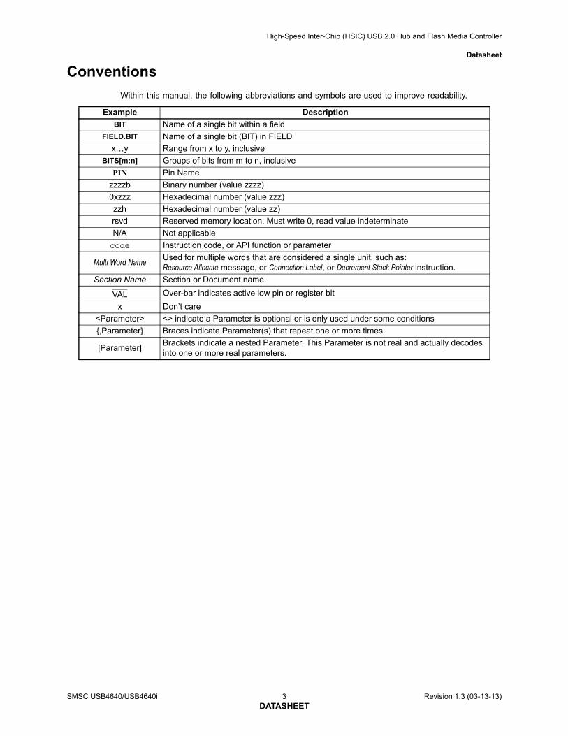
Conventions
Within this manual, the following abbreviations and symbols are used to improve readability.
Example Description
BIT Name of a single bit within a field
FIELD.BIT Name of a single bit (BIT) in FIELD
x…y Range from x to y, inclusive
BITS[m:n] Groups of bits from m to n, inclusive
PIN Pin Name
zzzzb Binary number (value zzzz)
0xzzz Hexadecimal number (value zzz)
zzh Hexadecimal number (value zz)
rsvd Reserved memory location. Must write 0, read value indeterminate
N/A Not applicable
code Instruction code, or API function or parameter
Multi Word Name Used for multiple words that are considered a single unit, such as:Resource Allocate message, or Connection Label, or Decrement Stack Pointer instruction.
Section Name Section or Document name.
VAL Over-bar indicates active low pin or register bit
x Don’t care
<Parameter> <> indicate a Parameter is optional or is only used under some conditions
{,Parameter} Braces indicate Parameter(s) that repeat one or more times.
[Parameter]Brackets indicate a nested Parameter. This Parameter is not real and actually decodes into one or more real parameters.
High-Speed Inter-Chip (HSIC) USB 2.0 Hub and Flash Media Controller
Datasheet
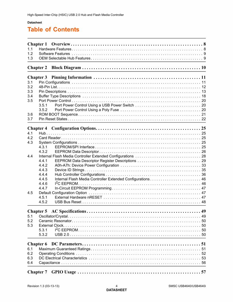
Table of Contents
Chapter 1 Overview . . . . . . . . . . . . . . . . . . . . . . . . . . . . . . . . . . . . . . . . . . . . . . . . . . . . . . . . . . 81.1 Hardware Features . . . . . . . . . . . . . . . . . . . . . . . . . . . . . . . . . . . . . . . . . . . . . . . . . . . . . . . . . . . . . . 81.2 Software Features . . . . . . . . . . . . . . . . . . . . . . . . . . . . . . . . . . . . . . . . . . . . . . . . . . . . . . . . . . . . . . 91.3 OEM Selectable Hub Features . . . . . . . . . . . . . . . . . . . . . . . . . . . . . . . . . . . . . . . . . . . . . . . . . . . . . 9
Chapter 2 Block Diagram . . . . . . . . . . . . . . . . . . . . . . . . . . . . . . . . . . . . . . . . . . . . . . . . . . . . 10
Chapter 3 Pinning Information . . . . . . . . . . . . . . . . . . . . . . . . . . . . . . . . . . . . . . . . . . . . . . . 113.1 Pin Configurations . . . . . . . . . . . . . . . . . . . . . . . . . . . . . . . . . . . . . . . . . . . . . . . . . . . . . . . . . . . . . 113.2 48-Pin List. . . . . . . . . . . . . . . . . . . . . . . . . . . . . . . . . . . . . . . . . . . . . . . . . . . . . . . . . . . . . . . . . . . . 123.3 Pin Descriptions . . . . . . . . . . . . . . . . . . . . . . . . . . . . . . . . . . . . . . . . . . . . . . . . . . . . . . . . . . . . . . . 133.4 Buffer Type Descriptions . . . . . . . . . . . . . . . . . . . . . . . . . . . . . . . . . . . . . . . . . . . . . . . . . . . . . . . . 183.5 Port Power Control . . . . . . . . . . . . . . . . . . . . . . . . . . . . . . . . . . . . . . . . . . . . . . . . . . . . . . . . . . . . . 20
3.5.1 Port Power Control Using a USB Power Switch . . . . . . . . . . . . . . . . . . . . . . . . . . . . . . . 203.5.2 Port Power Control Using a Poly Fuse . . . . . . . . . . . . . . . . . . . . . . . . . . . . . . . . . . . . . . 20
3.6 ROM BOOT Sequence . . . . . . . . . . . . . . . . . . . . . . . . . . . . . . . . . . . . . . . . . . . . . . . . . . . . . . . . . . 213.7 Pin Reset States . . . . . . . . . . . . . . . . . . . . . . . . . . . . . . . . . . . . . . . . . . . . . . . . . . . . . . . . . . . . . . . 22
Chapter 4 Configuration Options. . . . . . . . . . . . . . . . . . . . . . . . . . . . . . . . . . . . . . . . . . . . . . 254.1 Hub . . . . . . . . . . . . . . . . . . . . . . . . . . . . . . . . . . . . . . . . . . . . . . . . . . . . . . . . . . . . . . . . . . . . . . . . . 254.2 Card Reader . . . . . . . . . . . . . . . . . . . . . . . . . . . . . . . . . . . . . . . . . . . . . . . . . . . . . . . . . . . . . . . . . . 254.3 System Configurations . . . . . . . . . . . . . . . . . . . . . . . . . . . . . . . . . . . . . . . . . . . . . . . . . . . . . . . . . . 25
4.3.1 EEPROM/SPI Interface . . . . . . . . . . . . . . . . . . . . . . . . . . . . . . . . . . . . . . . . . . . . . . . . . . 254.3.2 EEPROM Data Descriptor . . . . . . . . . . . . . . . . . . . . . . . . . . . . . . . . . . . . . . . . . . . . . . . . 26
4.4 Internal Flash Media Controller Extended Configurations . . . . . . . . . . . . . . . . . . . . . . . . . . . . . . . 284.4.1 EEPROM Data Descriptor Register Descriptions . . . . . . . . . . . . . . . . . . . . . . . . . . . . . . 294.4.2 A0h-A7h: Device Power Configuration . . . . . . . . . . . . . . . . . . . . . . . . . . . . . . . . . . . . . . 334.4.3 Device ID Strings. . . . . . . . . . . . . . . . . . . . . . . . . . . . . . . . . . . . . . . . . . . . . . . . . . . . . . . 354.4.4 Hub Controller Configurations . . . . . . . . . . . . . . . . . . . . . . . . . . . . . . . . . . . . . . . . . . . . . 364.4.5 Internal Flash Media Controller Extended Configurations . . . . . . . . . . . . . . . . . . . . . . . . 464.4.6 I2C EEPROM. . . . . . . . . . . . . . . . . . . . . . . . . . . . . . . . . . . . . . . . . . . . . . . . . . . . . . . . . . 464.4.7 In-Circuit EEPROM Programming . . . . . . . . . . . . . . . . . . . . . . . . . . . . . . . . . . . . . . . . . . 47
4.5 Default Configuration Option . . . . . . . . . . . . . . . . . . . . . . . . . . . . . . . . . . . . . . . . . . . . . . . . . . . . . 474.5.1 External Hardware nRESET . . . . . . . . . . . . . . . . . . . . . . . . . . . . . . . . . . . . . . . . . . . . . . 474.5.2 USB Bus Reset . . . . . . . . . . . . . . . . . . . . . . . . . . . . . . . . . . . . . . . . . . . . . . . . . . . . . . . . 48
Chapter 5 AC Specifications . . . . . . . . . . . . . . . . . . . . . . . . . . . . . . . . . . . . . . . . . . . . . . . . . . 495.1 Oscillator/Crystal. . . . . . . . . . . . . . . . . . . . . . . . . . . . . . . . . . . . . . . . . . . . . . . . . . . . . . . . . . . . . . . 495.2 Ceramic Resonator. . . . . . . . . . . . . . . . . . . . . . . . . . . . . . . . . . . . . . . . . . . . . . . . . . . . . . . . . . . . . 505.3 External Clock. . . . . . . . . . . . . . . . . . . . . . . . . . . . . . . . . . . . . . . . . . . . . . . . . . . . . . . . . . . . . . . . . 50
5.3.1 I2C EEPROM. . . . . . . . . . . . . . . . . . . . . . . . . . . . . . . . . . . . . . . . . . . . . . . . . . . . . . . . . . 505.3.2 USB 2.0 . . . . . . . . . . . . . . . . . . . . . . . . . . . . . . . . . . . . . . . . . . . . . . . . . . . . . . . . . . . . . . 50
Chapter 6 DC Parameters . . . . . . . . . . . . . . . . . . . . . . . . . . . . . . . . . . . . . . . . . . . . . . . . . . . . 516.1 Maximum Guaranteed Ratings . . . . . . . . . . . . . . . . . . . . . . . . . . . . . . . . . . . . . . . . . . . . . . . . . . . . 516.2 Operating Conditions . . . . . . . . . . . . . . . . . . . . . . . . . . . . . . . . . . . . . . . . . . . . . . . . . . . . . . . . . . . 526.3 DC Electrical Characteristics . . . . . . . . . . . . . . . . . . . . . . . . . . . . . . . . . . . . . . . . . . . . . . . . . . . . . 536.4 Capacitance . . . . . . . . . . . . . . . . . . . . . . . . . . . . . . . . . . . . . . . . . . . . . . . . . . . . . . . . . . . . . . . . . . 56
Chapter 7 GPIO Usage . . . . . . . . . . . . . . . . . . . . . . . . . . . . . . . . . . . . . . . . . . . . . . . . . . . . . . 57
Revision 1.3 (03-13-13) 4 SMSC USB4640/USB4640iDATASHEET
High-Speed Inter-Chip (HSIC) USB 2.0 Hub and Flash Media Controller
Datasheet
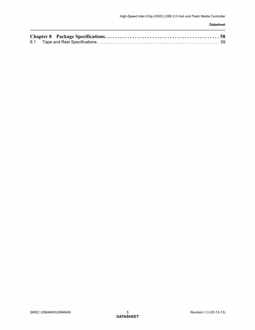
Chapter 8 Package Specifications. . . . . . . . . . . . . . . . . . . . . . . . . . . . . . . . . . . . . . . . . . . . . . 588.1 Tape and Reel Specifications . . . . . . . . . . . . . . . . . . . . . . . . . . . . . . . . . . . . . . . . . . . . . . . . . . . . . 59
SMSC USB4640/USB4640i 5 Revision 1.3 (03-13-13)DATASHEET
High-Speed Inter-Chip (HSIC) USB 2.0 Hub and Flash Media Controller
Datasheet
Revision 1.3 (03-13-13) 6 SMSC USB4640/USB4640iDATASHEET
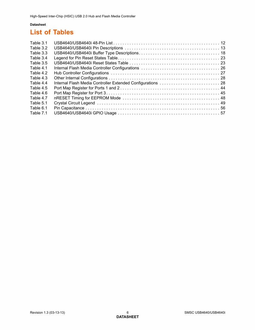
List of Tables
Table 3.1 USB4640/USB4640i 48-Pin List . . . . . . . . . . . . . . . . . . . . . . . . . . . . . . . . . . . . . . . . . . . . . . 12Table 3.2 USB4640/USB4640i Pin Descriptions . . . . . . . . . . . . . . . . . . . . . . . . . . . . . . . . . . . . . . . . . 13Table 3.3 USB4640/USB4640i Buffer Type Descriptions. . . . . . . . . . . . . . . . . . . . . . . . . . . . . . . . . . . 18Table 3.4 Legend for Pin Reset States Table. . . . . . . . . . . . . . . . . . . . . . . . . . . . . . . . . . . . . . . . . . . . 23Table 3.5 USB4640/USB4640i Reset States Table . . . . . . . . . . . . . . . . . . . . . . . . . . . . . . . . . . . . . . . 23Table 4.1 Internal Flash Media Controller Configurations . . . . . . . . . . . . . . . . . . . . . . . . . . . . . . . . . . 26Table 4.2 Hub Controller Configurations . . . . . . . . . . . . . . . . . . . . . . . . . . . . . . . . . . . . . . . . . . . . . . . 27Table 4.3 Other Internal Configurations . . . . . . . . . . . . . . . . . . . . . . . . . . . . . . . . . . . . . . . . . . . . . . . . 28Table 4.4 Internal Flash Media Controller Extended Configurations . . . . . . . . . . . . . . . . . . . . . . . . . . 28Table 4.5 Port Map Register for Ports 1 and 2 . . . . . . . . . . . . . . . . . . . . . . . . . . . . . . . . . . . . . . . . . . . 44Table 4.6 Port Map Register for Port 3 . . . . . . . . . . . . . . . . . . . . . . . . . . . . . . . . . . . . . . . . . . . . . . . . . 45Table 4.7 nRESET Timing for EEPROM Mode . . . . . . . . . . . . . . . . . . . . . . . . . . . . . . . . . . . . . . . . . . 48Table 5.1 Crystal Circuit Legend . . . . . . . . . . . . . . . . . . . . . . . . . . . . . . . . . . . . . . . . . . . . . . . . . . . . . 49Table 6.1 Pin Capacitance . . . . . . . . . . . . . . . . . . . . . . . . . . . . . . . . . . . . . . . . . . . . . . . . . . . . . . . . . . 56Table 7.1 USB4640/USB4640i GPIO Usage . . . . . . . . . . . . . . . . . . . . . . . . . . . . . . . . . . . . . . . . . . . . 57
High-Speed Inter-Chip (HSIC) USB 2.0 Hub and Flash Media Controller
Datasheet
SMSC USB4640/USB4640i 7 Revision 1.3 (03-13-13)DATASHEET
List of Figures
Figure 2.1 USB4640/USB4640i Block Diagram. . . . . . . . . . . . . . . . . . . . . . . . . . . . . . . . . . . . . . . . . . . 10Figure 3.1 USB4640/USB4640i 48-Pin QFN . . . . . . . . . . . . . . . . . . . . . . . . . . . . . . . . . . . . . . . . . . . . . 11Figure 3.2 Port Power Control with USB Power Switch. . . . . . . . . . . . . . . . . . . . . . . . . . . . . . . . . . . . . 20Figure 3.3 Port Power Control with a Single Poly Fuse and Multiple Loads . . . . . . . . . . . . . . . . . . . . . 21Figure 3.4 Port Power with Ganged Control with Poly Fuse . . . . . . . . . . . . . . . . . . . . . . . . . . . . . . . . . 21Figure 3.5 SPI ROM Connection . . . . . . . . . . . . . . . . . . . . . . . . . . . . . . . . . . . . . . . . . . . . . . . . . . . . . . 22Figure 3.6 I2C Connection . . . . . . . . . . . . . . . . . . . . . . . . . . . . . . . . . . . . . . . . . . . . . . . . . . . . . . . . . . . 22Figure 3.7 Pin Reset States . . . . . . . . . . . . . . . . . . . . . . . . . . . . . . . . . . . . . . . . . . . . . . . . . . . . . . . . . . 22Figure 4.1 nRESET Timing for EEPROM Mode . . . . . . . . . . . . . . . . . . . . . . . . . . . . . . . . . . . . . . . . . . 47Figure 5.1 Typical Crystal Circuit . . . . . . . . . . . . . . . . . . . . . . . . . . . . . . . . . . . . . . . . . . . . . . . . . . . . . . 49Figure 5.2 Capacitance Formulas . . . . . . . . . . . . . . . . . . . . . . . . . . . . . . . . . . . . . . . . . . . . . . . . . . . . . 49Figure 5.3 Ceramic Resonator Usage with SMSC IC . . . . . . . . . . . . . . . . . . . . . . . . . . . . . . . . . . . . . . 50Figure 6.1 Supply Rise Time Model . . . . . . . . . . . . . . . . . . . . . . . . . . . . . . . . . . . . . . . . . . . . . . . . . . . . 52Figure 8.1 USB4640/USB4640i 48-Pin QFN . . . . . . . . . . . . . . . . . . . . . . . . . . . . . . . . . . . . . . . . . . . . . 58Figure 8.2 48-Pin Package Tape Specifications . . . . . . . . . . . . . . . . . . . . . . . . . . . . . . . . . . . . . . . . . . 59Figure 8.3 48-Pin Package Reel Specifications. . . . . . . . . . . . . . . . . . . . . . . . . . . . . . . . . . . . . . . . . . . 60
High-Speed Inter-Chip (HSIC) USB 2.0 Hub and Flash Media Controller
Datasheet
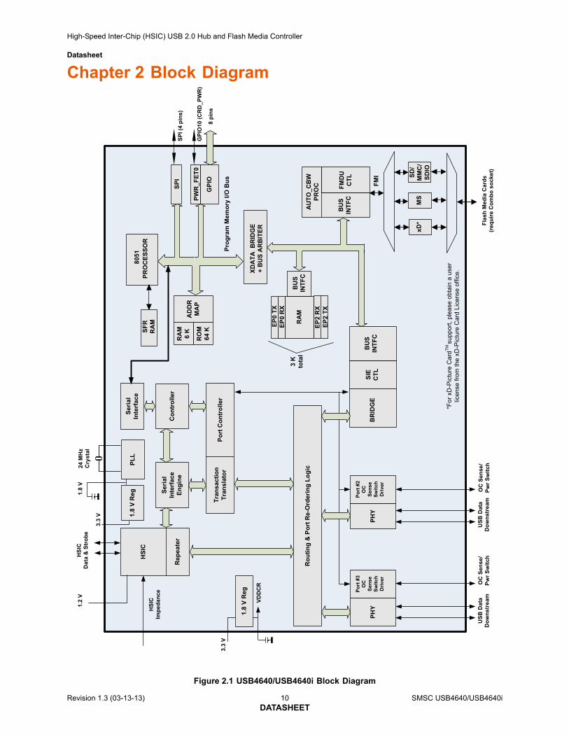
Chapter 1 Overview
The USB4640/USB4640i is a Hi-Speed HSIC USB hub and card reader combo solution with anupstream port compliant to the High-Speed Inter-Chip USB Electrical Specification Revision 1.0 [2].The two downstream ports are USB 2.0 compliant, and the dedicated flash media reader/writer isinternally attached to a 3rd downstream port as a USB compound device.
High-Speed Inter-Chip (HSIC) is a digital interconnect bus that enables the use of USB technologyas a low-power chip-to-chip interconnect at speeds up to 480 Mb/s (see the High-Speed Inter-ChipUSB Electrical Specification Revision 1.0). This combo solution supports several multi-format flashmedia cards. This multi-format flash media controller and USB hub combo features two exposeddownstream USB ports available for external peripheral expansion.
The USB4640/USB4640i can attach to an upstream port as a Full- or Full/Hi-Speed hub. The hubsupports Low-Speed, Full-Speed, and Hi-Speed downstream devices (if operating as a Hi-Speedhub) on all of the enabled downstream ports.
All required resistors on the USB ports are integrated into the hub, including all series terminationresistors on D+ and D– pins and all required pull-down and pull-up resistors. The over-current senseinputs for the downstream facing ports have internal pull-up resistors.
The USB4640/USB4640i includes programmable features, such as:
PortMap: provides flexible port mapping and disable sequences. The downstream ports of a USB4640/USB4640i hub can be reordered or disabled in any sequence to support multiple platform designs with minimum effort. For any port that is disabled, the USB4640/USB4640i hub controllers automatically reorder the remaining ports to match the USB host controller’s port numbering scheme.
PortSwap: adds per-port programmability to USB differential-pair pin locations. PortSwap also allows direct alignment of USB signals (D+/D-) to connectors to avoid uneven trace length or crossing of the USB differential signals on the PCB.
PHYBoost: enables 4 programmable levels of USB signal drive strength in downstream port transceivers. PHYBoost will also attempt to restore USB signal integrity.
Note: PHYBoost is only available on the two USB downstreamports.
1.1 Hardware Features
Single chip HSIC hub and flash media controller combo
USB2660/USB2660i supports the commercial temperature range of 0°C to +70°C
USB4640/USB4640i supports the industrial temperature range of -40°C to +85°C
Transaction translator (TT) in the hub supports operation of FS and LS peripherals
Full power management with individual or ganged power control of each downstream port
Optional support for external firmware access via SPI interface
Onboard 24 MHz crystal driver circuit
Optional external 24 MHz clock input (must be a 1.8 V signal)
Code execution via SPI ROM which must meet the following criteria:
—30 MHz or 60 MHz operation support
—Single bit or dual bit mode support
—Mode 0 or mode 3 SPI support
Revision 1.3 (03-13-13) 8 SMSC USB4640/USB4640iDATASHEET
High-Speed Inter-Chip (HSIC) USB 2.0 Hub and Flash Media Controller
Datasheet
Compliance with the following flash media card specifications:
—Secure Digital 2.0 and MultiMediaCard 4.2–SD 2.0, SD-HS, SD-HC–TransFlash™ and reduced form factor media–1/4/8 bit MMC 4.2
—Memory Stick 1.43
—Memory Stick Pro Format 1.02
—Memory Stick Pro-HG Duo Format 1.01 –Memory Stick, MS Duo, MS-HS, MS Pro-HG, MS Pro
—Memory Stick Duo 1.10–xD-Picture Card 1.2
Up to 9 GPIOs: configuration and polarity for special function use
—The number of actual GPIOs depends on the implementation configuration used
—One GPIO available with up to 200 mA drive and protected fold-back short circuit current
8051 8-bit microprocessor
—60 MHz - single cycle execution
—64 KB ROM | 9 KB RAM
Integrated regulator for 1.8 V core operation
1.2 Software Features
Hub and flash media reader/writer configuration from a single source: External I2C ROM or external SPI ROM, where the following features are then available:
—Customizable vendor ID, product ID, and device ID
—12-hex digits maximum for the serial number string
—28-character manufacturer ID and product strings for the flash media reader/writer
1.3 OEM Selectable Hub Features
The USB4640/USB4640i provides a default configuration that may be sufficient for most applications.following a reset. The USB4640/USB4640i can instead be configured by an external I2C EEPROM orSPI ROM.
Compound Device support on a port-by-port basis
—a port is permanently hardwired to a downstream USB peripheral device
Select over-current sensing and port power control on an individual or ganged (all ports together) basis to match the OEM’s choice of circuit board component selection
Port power control and over-current detection/delay features
Configure the delay time for filtering the over-current sense inputs
Configure the delay time for turning on downstream port power
Bus- or self-powered selection
Hub port disable or non-removable configurations
Flexible port mapping and disable sequencing supports multiple platform designs
Programmable USB differential-pair pin location eases PCB layout by aligning USB signal lines directly to connectors
Programmable USB signal drive strength recovers USB signal integrity using 4 levels of signal drive strength
Indicate the maximum current that the 2-port hub consumes
Indicate the maximum current required for the hub controller
SMSC USB4640/USB4640i 9 Revision 1.3 (03-13-13)DATASHEET
High-Speed Inter-Chip (HSIC) USB 2.0 Hub and Flash Media Controller
Datasheet
Revision 1.3 (03-13-13) 10 SMSC USB4640/USB4640iDATASHEET
Chapter 2 Block Diagram
Figure 2.1 USB4640/USB4640i Block Diagram
1.2
V
HS
IC
HS
IC
Da
ta &
Str
ob
e
Rep
eate
rC
on
tro
ller
Se
rial
In
terf
ace
E
ng
ine
Ser
ial
Inte
rfac
e
Ro
uti
ng
& P
ort
Re
-Ord
erin
g L
og
ic
Po
rt C
on
tro
ller
PH
Y
Po
rt #
3O
C
Sen
seS
wit
ch
Dri
ver
Tra
nsa
cti
on
Tra
ns
lato
r
PH
Y
Po
rt #
2O
C
Sen
seS
wit
ch
Dri
ver
US
B D
ata
Do
wn
stre
amO
C S
ense
/P
wr
Sw
itch
805
1P
RO
CE
SS
OR
SF
R
RA
M
XD
AT
A B
RID
GE
+ B
US
AR
BIT
ER
RO
M
64
K
RA
M6
KA
DD
RM
AP
GP
IOs
Pro
gra
m M
emo
ry I/
O B
us
PW
R_F
ET
0
8 p
ins
GP
IO10
(C
RD
_P
WR
)
GP
IO
3 K
tota
lR
AM
EP
2 T
XE
P2
RX
BU
S
INT
FC
EP
2 R
X
EP
0 T
XE
P0
RX
SIE
CT
LB
RID
GE
BU
S
INT
FC
FM
DU
CT
L
AU
TO
_CB
W
PR
OC F
MI
BU
S
INT
FC
US
B D
ata
Do
wn
stre
amF
lash
Med
ia C
ard
s
(req
uir
e C
om
bo
so
cke
t)
MS
xD*
SD
/M
MC
/S
DIO
OC
Sen
se/
Pw
r S
wit
ch
SP
IS
PI (
4 p
ins
)
3.3
V
1.8
V
PL
L
24 M
Hz
Cry
stal
1.8
V R
eg
*Fo
r xD
-Pic
ture
Ca
rdT
M su
ppor
t, pl
ease
obt
ain
a u
ser
lice
nse
from
the
xD
-Pic
ture
Car
d L
ice
nse
offic
e.
3.3
V
1.8
V R
eg
VD
DC
R
HS
IC
Imp
ed
an
ce
High-Speed Inter-Chip (HSIC) USB 2.0 Hub and Flash Media Controller
Datasheet
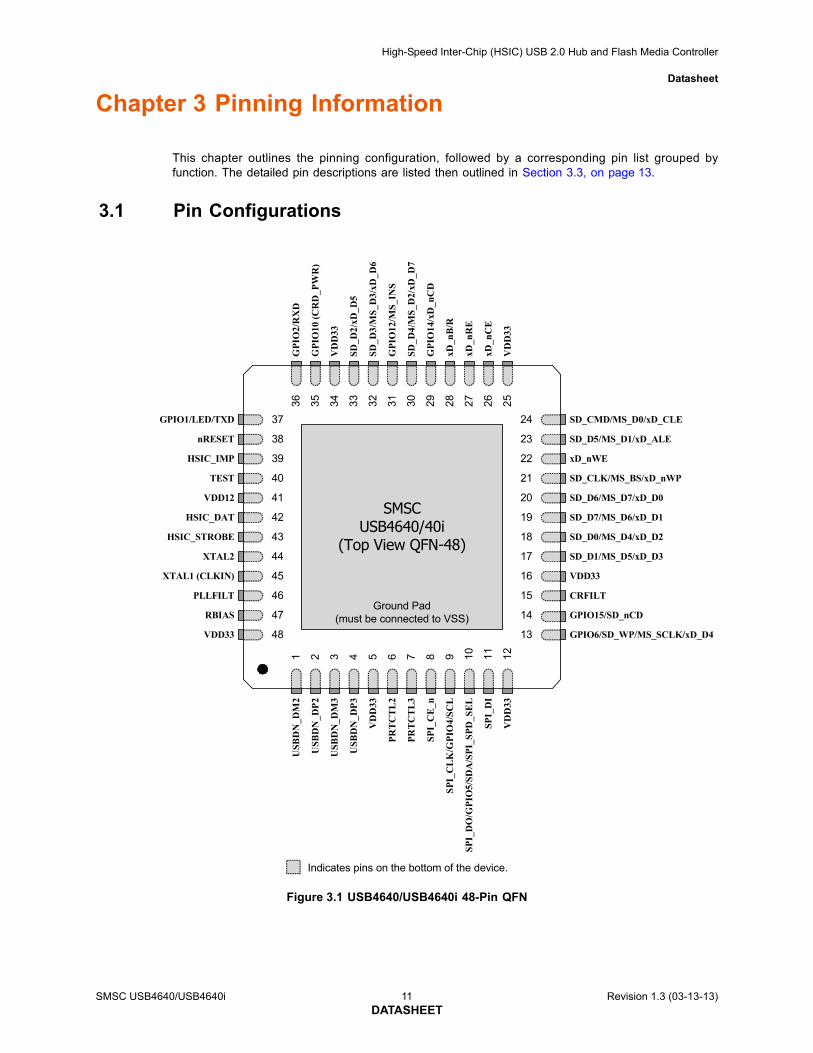
Chapter 3 Pinning Information
This chapter outlines the pinning configuration, followed by a corresponding pin list grouped byfunction. The detailed pin descriptions are listed then outlined in Section 3.3, on page 13.
3.1 Pin Configurations
Figure 3.1 USB4640/USB4640i 48-Pin QFN
Ground Pad(must be connected to VSS)
SMSCUSB4640/40i
(Top View QFN-48)
nRESET 38
39
GPIO1/LED/TXD 37
TEST 40
VDD12 41
HSIC_STROBE 43
XTAL2 44
XTAL1 (CLKIN) 45
RBIAS
48VDD33
47
PLLFILT 46
HSIC_DAT 42
VD
D33
1U
SBD
N_D
M2
2U
SBD
N_D
P2
3U
SBD
N_D
M3
4U
SBD
N_D
P3
5
PR
TC
TL
26
PR
TC
TL
37
SP
I_C
E_n
8
SP
I_C
LK
/GP
IO4/
SC
L9
VD
D33
10
SP
I_D
I1
1
SP
I_D
O/G
PIO
5/S
DA
/SP
I_S
PD
_SE
L
12
21 SD_CLK/MS_BS/xD_nWP
20 SD_D6/MS_D7/xD_D0
19 SD_D7/MS_D6/xD_D1
18 SD_D0/MS_D4/xD_D2
17
CRFILT
16
SD_D1/MS_D5/xD_D3
15
VDD33
14 GPIO15/SD_nCD
13 GPIO6/SD_WP/MS_SCLK/xD_D4
23 SD_D5/MS_D1/xD_ALE
22 xD_nWE
24
35
GP
IO2/
RX
D
34
GP
IO10
(C
RD
_PW
R)
33
VD
D33
32S
D_D
3/M
S_D
3/xD
_D6
31G
PIO
12/M
S_IN
S
30S
D_D
4/M
S_D
2/xD
_D7
29G
PIO
14/x
D_n
CD
28xD
_nB
/R
36
SD
_D2/
xD_D
5
27xD
_nR
E
26xD
_nC
E
25V
DD
33
SD_CMD/MS_D0/xD_CLE
HSIC_IMP
Indicates pins on the bottom of the device.
SMSC USB4640/USB4640i 11 Revision 1.3 (03-13-13)DATASHEET
High-Speed Inter-Chip (HSIC) USB 2.0 Hub and Flash Media Controller
Datasheet
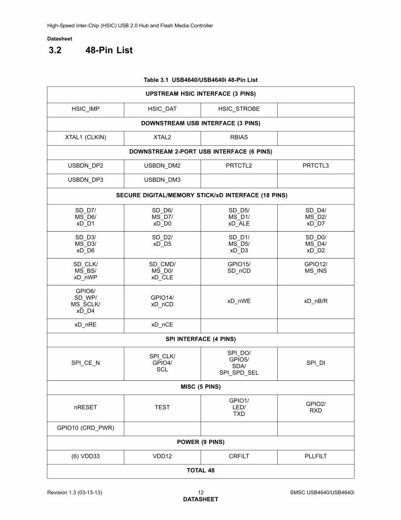
3.2 48-Pin List
Table 3.1 USB4640/USB4640i 48-Pin List
UPSTREAM HSIC INTERFACE (3 PINS)
HSIC_IMP HSIC_DAT HSIC_STROBE
DOWNSTREAM USB INTERFACE (3 PINS)
XTAL1 (CLKIN) XTAL2 RBIAS
DOWNSTREAM 2-PORT USB INTERFACE (6 PINS)
USBDN_DP2 USBDN_DM2 PRTCTL2 PRTCTL3
USBDN_DP3 USBDN_DM3
SECURE DIGITAL/MEMORY STICK/xD INTERFACE (18 PINS)
SD_D7/MS_D6/xD_D1
SD_D6/MS_D7/xD_D0
SD_D5/MS_D1/xD_ALE
SD_D4/MS_D2/xD_D7
SD_D3/MS_D3/xD_D6
SD_D2/xD_D5
SD_D1/MS_D5/xD_D3
SD_D0/MS_D4/xD_D2
SD_CLK/MS_BS/xD_nWP
SD_CMD/MS_D0/xD_CLE
GPIO15/SD_nCD
GPIO12/MS_INS
GPIO6/ SD_WP/
MS_SCLK/xD_D4
GPIO14/ xD_nCD
xD_nWE xD_nB/R
xD_nRE xD_nCE
SPI INTERFACE (4 PINS)
SPI_CE_NSPI_CLK/GPIO4/
SCL
SPI_DO/GPIO5/SDA/
SPI_SPD_SEL
SPI_DI
MISC (5 PINS)
nRESET TESTGPIO1/
LED/TXD
GPIO2/RXD
GPIO10 (CRD_PWR)
POWER (9 PINS)
(6) VDD33 VDD12 CRFILT PLLFILT
TOTAL 48
Revision 1.3 (03-13-13) 12 SMSC USB4640/USB4640iDATASHEET
High-Speed Inter-Chip (HSIC) USB 2.0 Hub and Flash Media Controller
Datasheet
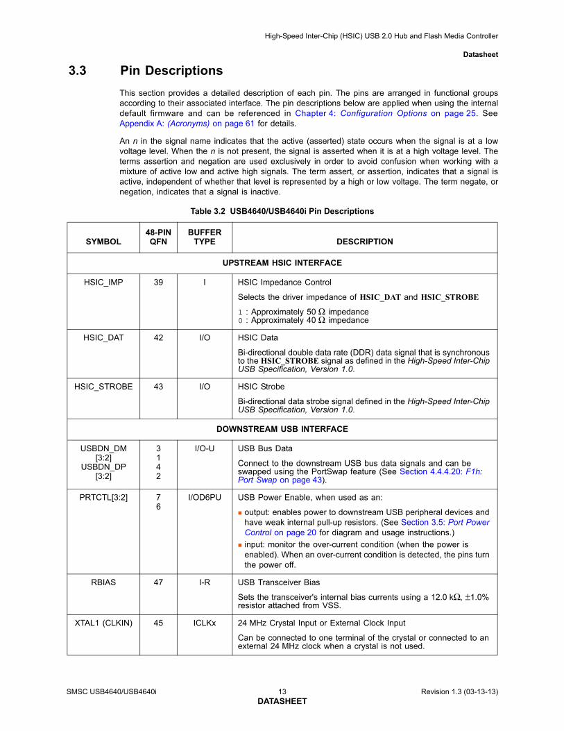
3.3 Pin Descriptions
This section provides a detailed description of each pin. The pins are arranged in functional groupsaccording to their associated interface. The pin descriptions below are applied when using the internaldefault firmware and can be referenced in Chapter 4: Configuration Options on page 25. SeeAppendix A: (Acronyms) on page 61 for details.
An n in the signal name indicates that the active (asserted) state occurs when the signal is at a lowvoltage level. When the n is not present, the signal is asserted when it is at a high voltage level. Theterms assertion and negation are used exclusively in order to avoid confusion when working with amixture of active low and active high signals. The term assert, or assertion, indicates that a signal isactive, independent of whether that level is represented by a high or low voltage. The term negate, ornegation, indicates that a signal is inactive.
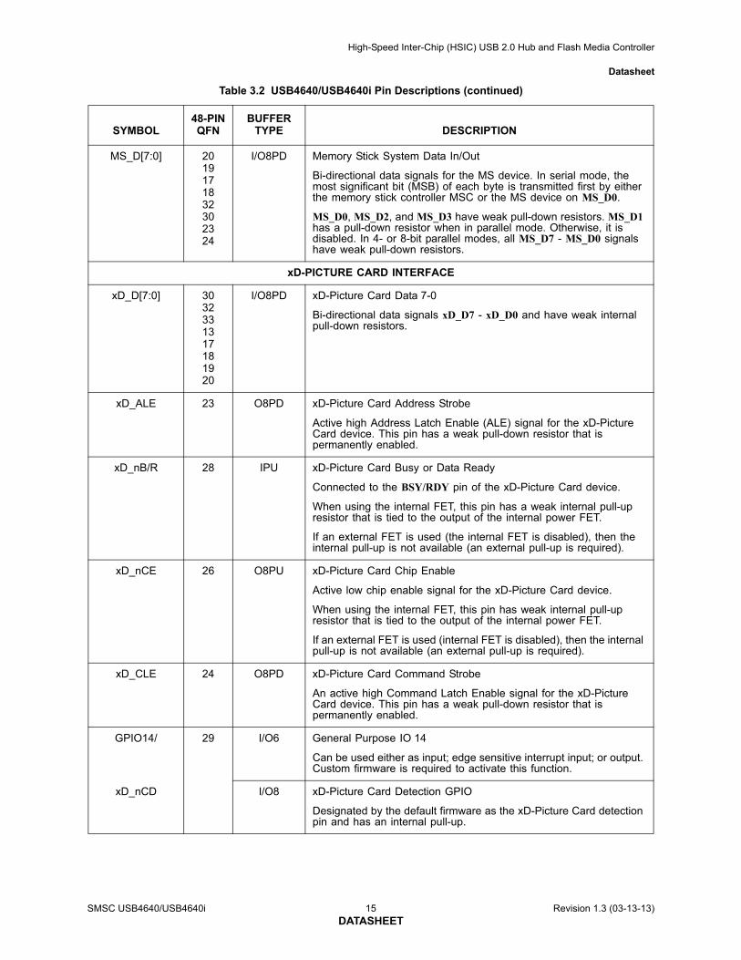
Table 3.2 USB4640/USB4640i Pin Descriptions
SYMBOL48-PIN QFN
BUFFER TYPE DESCRIPTION
UPSTREAM HSIC INTERFACE
HSIC_IMP 39 I HSIC Impedance Control
Selects the driver impedance of HSIC_DAT and HSIC_STROBE
1 : Approximately 50 Ω impedance0 : Approximately 40 Ω impedance
HSIC_DAT 42 I/O HSIC Data
Bi-directional double data rate (DDR) data signal that is synchronous to the HSIC_STROBE signal as defined in the High-Speed Inter-Chip USB Specification, Version 1.0.
HSIC_STROBE 43 I/O HSIC Strobe
Bi-directional data strobe signal defined in the High-Speed Inter-Chip USB Specification, Version 1.0.
DOWNSTREAM USB INTERFACE
USBDN_DM[3:2]
USBDN_DP[3:2]
3142
I/O-U USB Bus Data
Connect to the downstream USB bus data signals and can be swapped using the PortSwap feature (See Section 4.4.4.20: F1h: Port Swap on page 43).
PRTCTL[3:2] 76
I/OD6PU USB Power Enable, when used as an:
output: enables power to downstream USB peripheral devices and have weak internal pull-up resistors. (See Section 3.5: Port Power Control on page 20 for diagram and usage instructions.)
input: monitor the over-current condition (when the power is enabled). When an over-current condition is detected, the pins turn the power off.
RBIAS 47 I-R USB Transceiver Bias
Sets the transceiver's internal bias currents using a 12.0 kΩ, ±1.0% resistor attached from VSS.
XTAL1 (CLKIN) 45 ICLKx 24 MHz Crystal Input or External Clock Input
Can be connected to one terminal of the crystal or connected to an external 24 MHz clock when a crystal is not used.
SMSC USB4640/USB4640i 13 Revision 1.3 (03-13-13)DATASHEET
High-Speed Inter-Chip (HSIC) USB 2.0 Hub and Flash Media Controller
Datasheet
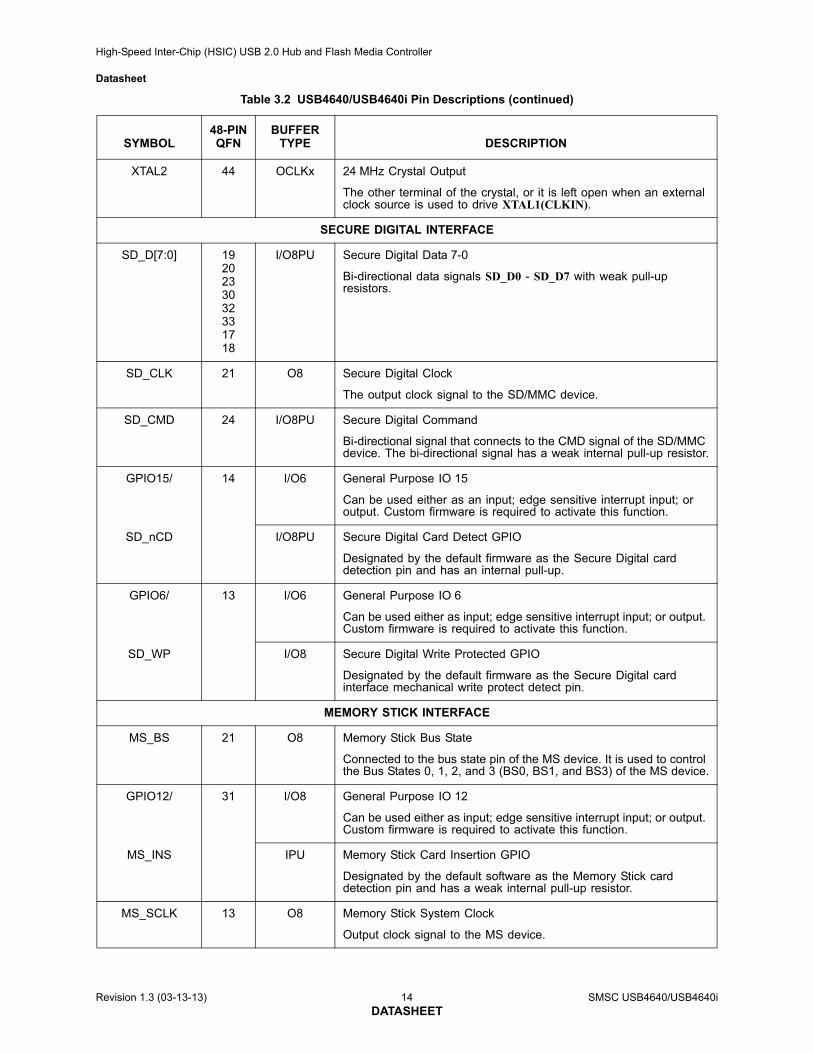
XTAL2 44 OCLKx 24 MHz Crystal Output
The other terminal of the crystal, or it is left open when an external clock source is used to drive XTAL1(CLKIN).
SECURE DIGITAL INTERFACE
SD_D[7:0] 1920233032331718
I/O8PU Secure Digital Data 7-0
Bi-directional data signals SD_D0 - SD_D7 with weak pull-up resistors.
SD_CLK 21 O8 Secure Digital Clock
The output clock signal to the SD/MMC device.
SD_CMD 24 I/O8PU Secure Digital Command
Bi-directional signal that connects to the CMD signal of the SD/MMC device. The bi-directional signal has a weak internal pull-up resistor.
GPIO15/ 14 I/O6 General Purpose IO 15
Can be used either as an input; edge sensitive interrupt input; or output. Custom firmware is required to activate this function.
SD_nCD I/O8PU Secure Digital Card Detect GPIO
Designated by the default firmware as the Secure Digital card detection pin and has an internal pull-up.
GPIO6/ 13 I/O6 General Purpose IO 6
Can be used either as input; edge sensitive interrupt input; or output. Custom firmware is required to activate this function.
SD_WP I/O8 Secure Digital Write Protected GPIO
Designated by the default firmware as the Secure Digital card interface mechanical write protect detect pin.
MEMORY STICK INTERFACE
MS_BS 21 O8 Memory Stick Bus State
Connected to the bus state pin of the MS device. It is used to control the Bus States 0, 1, 2, and 3 (BS0, BS1, and BS3) of the MS device.
GPIO12/ 31 I/O8 General Purpose IO 12
Can be used either as input; edge sensitive interrupt input; or output. Custom firmware is required to activate this function.
MS_INS IPU Memory Stick Card Insertion GPIO
Designated by the default software as the Memory Stick card detection pin and has a weak internal pull-up resistor.
MS_SCLK 13 O8 Memory Stick System Clock
Output clock signal to the MS device.
Table 3.2 USB4640/USB4640i Pin Descriptions (continued)
SYMBOL48-PIN QFN
BUFFER TYPE DESCRIPTION
Revision 1.3 (03-13-13) 14 SMSC USB4640/USB4640iDATASHEET
High-Speed Inter-Chip (HSIC) USB 2.0 Hub and Flash Media Controller
Datasheet
MS_D[7:0] 2019171832302324
I/O8PD Memory Stick System Data In/Out
Bi-directional data signals for the MS device. In serial mode, the most significant bit (MSB) of each byte is transmitted first by either the memory stick controller MSC or the MS device on MS_D0.
MS_D0, MS_D2, and MS_D3 have weak pull-down resistors. MS_D1 has a pull-down resistor when in parallel mode. Otherwise, it is disabled. In 4- or 8-bit parallel modes, all MS_D7 - MS_D0 signals have weak pull-down resistors.
xD-PICTURE CARD INTERFACE
xD_D[7:0] 3032331317181920
I/O8PD xD-Picture Card Data 7-0
Bi-directional data signals xD_D7 - xD_D0 and have weak internal pull-down resistors.
xD_ALE 23 O8PD xD-Picture Card Address Strobe
Active high Address Latch Enable (ALE) signal for the xD-Picture Card device. This pin has a weak pull-down resistor that is permanently enabled.
xD_nB/R 28 IPU xD-Picture Card Busy or Data Ready
Connected to the BSY/RDY pin of the xD-Picture Card device.
When using the internal FET, this pin has a weak internal pull-up resistor that is tied to the output of the internal power FET.
If an external FET is used (the internal FET is disabled), then the internal pull-up is not available (an external pull-up is required).
xD_nCE 26 O8PU xD-Picture Card Chip Enable
Active low chip enable signal for the xD-Picture Card device.
When using the internal FET, this pin has weak internal pull-up resistor that is tied to the output of the internal power FET.
If an external FET is used (internal FET is disabled), then the internal pull-up is not available (an external pull-up is required).
xD_CLE 24 O8PD xD-Picture Card Command Strobe
An active high Command Latch Enable signal for the xD-Picture Card device. This pin has a weak pull-down resistor that is permanently enabled.
GPIO14/ 29 I/O6 General Purpose IO 14
Can be used either as input; edge sensitive interrupt input; or output. Custom firmware is required to activate this function.
xD_nCD I/O8 xD-Picture Card Detection GPIO
Designated by the default firmware as the xD-Picture Card detection pin and has an internal pull-up.
Table 3.2 USB4640/USB4640i Pin Descriptions (continued)
SYMBOL48-PIN QFN
BUFFER TYPE DESCRIPTION
SMSC USB4640/USB4640i 15 Revision 1.3 (03-13-13)DATASHEET
High-Speed Inter-Chip (HSIC) USB 2.0 Hub and Flash Media Controller
Datasheet
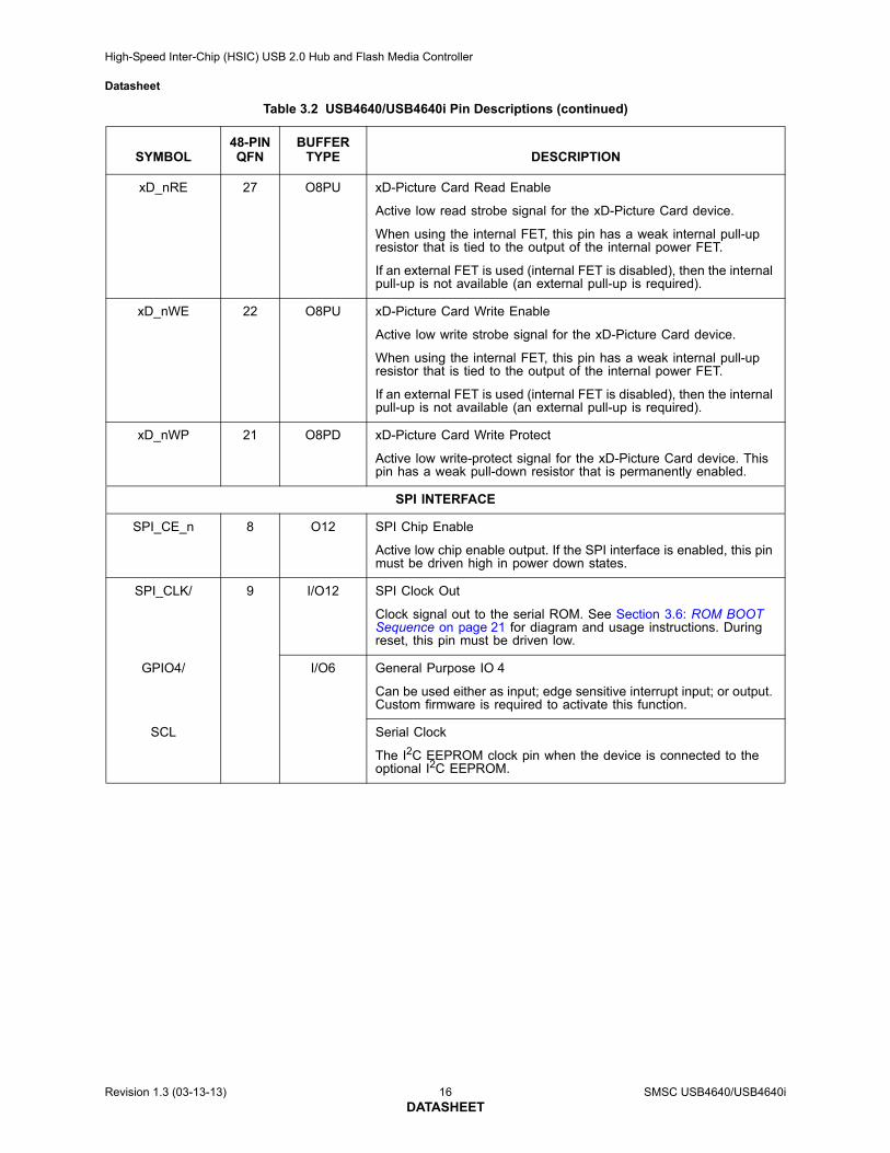
xD_nRE 27 O8PU xD-Picture Card Read Enable
Active low read strobe signal for the xD-Picture Card device.
When using the internal FET, this pin has a weak internal pull-up resistor that is tied to the output of the internal power FET.
If an external FET is used (internal FET is disabled), then the internal pull-up is not available (an external pull-up is required).
xD_nWE 22 O8PU xD-Picture Card Write Enable
Active low write strobe signal for the xD-Picture Card device.
When using the internal FET, this pin has a weak internal pull-up resistor that is tied to the output of the internal power FET.
If an external FET is used (internal FET is disabled), then the internal pull-up is not available (an external pull-up is required).
xD_nWP 21 O8PD xD-Picture Card Write Protect
Active low write-protect signal for the xD-Picture Card device. This pin has a weak pull-down resistor that is permanently enabled.
SPI INTERFACE
SPI_CE_n 8 O12 SPI Chip Enable
Active low chip enable output. If the SPI interface is enabled, this pin must be driven high in power down states.
SPI_CLK/ 9 I/O12 SPI Clock Out
Clock signal out to the serial ROM. See Section 3.6: ROM BOOT Sequence on page 21 for diagram and usage instructions. During reset, this pin must be driven low.
GPIO4/ I/O6 General Purpose IO 4
Can be used either as input; edge sensitive interrupt input; or output. Custom firmware is required to activate this function.
SCL Serial Clock
The I2C EEPROM clock pin when the device is connected to the optional I2C EEPROM.
Table 3.2 USB4640/USB4640i Pin Descriptions (continued)
SYMBOL48-PIN QFN
BUFFER TYPE DESCRIPTION
Revision 1.3 (03-13-13) 16 SMSC USB4640/USB4640iDATASHEET
High-Speed Inter-Chip (HSIC) USB 2.0 Hub and Flash Media Controller
Datasheet
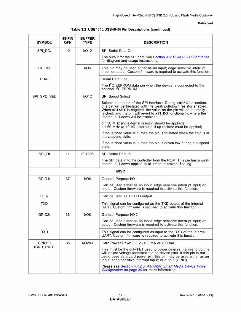
SPI_DO/ 10 I/O12 SPI Serial Data Out
The output for the SPI port. See Section 3.6: ROM BOOT Sequence for diagram and usage instructions.
GPIO5/ I/O6 This pin may be used either as an input; edge sensitive interrupt input; or output. Custom firmware is required to activate this function.
SDA/ Serial Data Line
The I2C EEPROM data pin when the device is connected to the optional I2C EEPROM.
SPI_SPD_SEL I/O12 SPI Speed Select
Selects the speed of the SPI interface. During nRESET assertion, this pin will be tri-stated with the weak pull-down resistor enabled. When nRESET is negated, the value on the pin will be internally latched, and the pin will revert to SPI_DO functionality, where the internal pull-down will be disabled.
0 : 30 MHz (no external resistor should be applied)1 : 60 MHz (a 10 kΩ external pull-up resistor must be applied)
If the latched value is 1, then the pin is tri-stated when the chip is in the suspend state.
If the latched value is 0, then the pin is driven low during a suspend state.
SPI_DI 11 I/O12PD SPI Serial Data In
The SPI data in to the controller from the ROM. This pin has a weak internal pull-down applied at all times to prevent floating.
MISC
GPIO1/ 37 I/O6 General Purpose I/O 1
Can be used either as an input; edge sensitive interrupt input; or output. Custom firmware is required to activate this function.
LED/ Can be used as an LED output.
TXD This signal can be configured as the TXD output of the internal UART. Custom firmware is required to activate this function.
GPIO2/ 36 I/O6 General Purpose I/O 2
Can be used either as an input; edge sensitive interrupt input; or output. Custom firmware is required to activate this function.
RXD This signal can be configured as input to the RXD of the internal UART. Custom firmware is required to activate this function.
GPIO10 (CRD_PWR)
35 I/O200 Card Power Drive: 3.3 V (100 mA or 200 mA)
This must be the only FET used to power devices. Failure to do this will violate voltage specifications on device pins. If this pin is not being used as a card power pin, this pin may be used either as an input; edge sensitive interrupt input; or output (GPIO).
Please see Section 4.4.2.3: A4h-A5h: Smart Media Device Power Configuration on page 34 for more information.
Table 3.2 USB4640/USB4640i Pin Descriptions (continued)
SYMBOL48-PIN QFN
BUFFER TYPE DESCRIPTION
SMSC USB4640/USB4640i 17 Revision 1.3 (03-13-13)DATASHEET
High-Speed Inter-Chip (HSIC) USB 2.0 Hub and Flash Media Controller
Datasheet
3.4 Buffer Type Descriptions
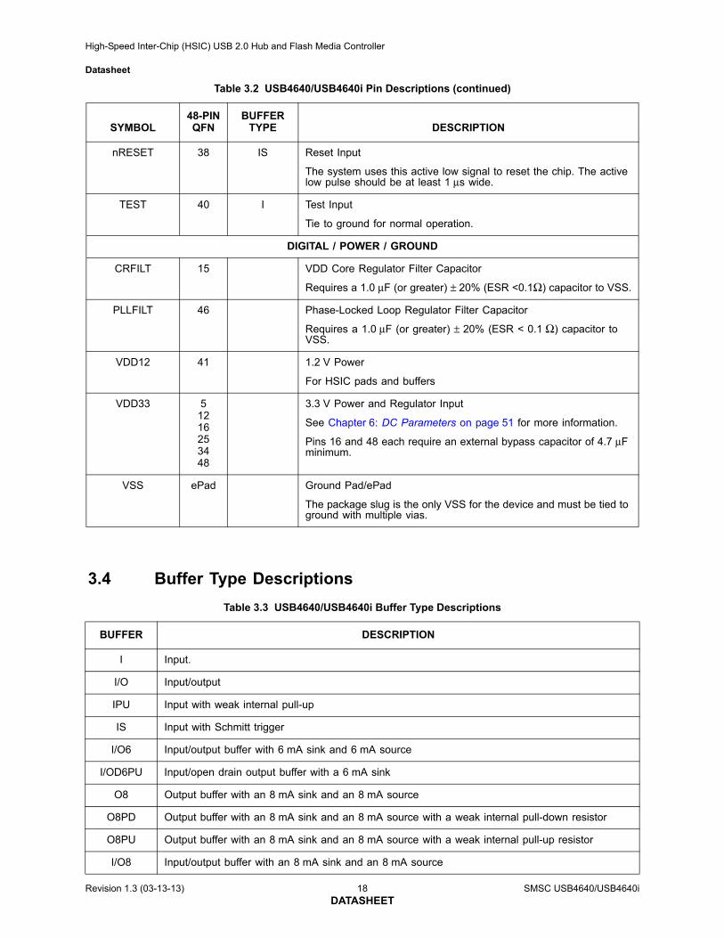
nRESET 38 IS Reset Input
The system uses this active low signal to reset the chip. The active low pulse should be at least 1 μs wide.
TEST 40 I Test Input
Tie to ground for normal operation.
DIGITAL / POWER / GROUND
CRFILT 15 VDD Core Regulator Filter Capacitor
Requires a 1.0 μF (or greater) ± 20% (ESR <0.1Ω) capacitor to VSS.
PLLFILT 46 Phase-Locked Loop Regulator Filter Capacitor
Requires a 1.0 μF (or greater) ± 20% (ESR < 0.1 Ω) capacitor to VSS.
VDD12 41 1.2 V Power
For HSIC pads and buffers
VDD33 51216253448
3.3 V Power and Regulator Input
See Chapter 6: DC Parameters on page 51 for more information.
Pins 16 and 48 each require an external bypass capacitor of 4.7 μF minimum.
VSS ePad Ground Pad/ePad
The package slug is the only VSS for the device and must be tied to ground with multiple vias.
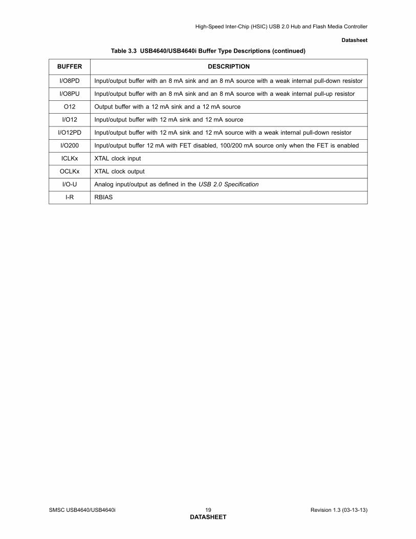
Table 3.3 USB4640/USB4640i Buffer Type Descriptions
BUFFER DESCRIPTION
I Input.
I/O Input/output
IPU Input with weak internal pull-up
IS Input with Schmitt trigger
I/O6 Input/output buffer with 6 mA sink and 6 mA source
I/OD6PU Input/open drain output buffer with a 6 mA sink
O8 Output buffer with an 8 mA sink and an 8 mA source
O8PD Output buffer with an 8 mA sink and an 8 mA source with a weak internal pull-down resistor
O8PU Output buffer with an 8 mA sink and an 8 mA source with a weak internal pull-up resistor
I/O8 Input/output buffer with an 8 mA sink and an 8 mA source
Table 3.2 USB4640/USB4640i Pin Descriptions (continued)
SYMBOL48-PIN QFN
BUFFER TYPE DESCRIPTION
Revision 1.3 (03-13-13) 18 SMSC USB4640/USB4640iDATASHEET
High-Speed Inter-Chip (HSIC) USB 2.0 Hub and Flash Media Controller
Datasheet
I/O8PD Input/output buffer with an 8 mA sink and an 8 mA source with a weak internal pull-down resistor
I/O8PU Input/output buffer with an 8 mA sink and an 8 mA source with a weak internal pull-up resistor
O12 Output buffer with a 12 mA sink and a 12 mA source
I/O12 Input/output buffer with 12 mA sink and 12 mA source
I/O12PD Input/output buffer with 12 mA sink and 12 mA source with a weak internal pull-down resistor
I/O200 Input/output buffer 12 mA with FET disabled, 100/200 mA source only when the FET is enabled
ICLKx XTAL clock input
OCLKx XTAL clock output
I/O-U Analog input/output as defined in the USB 2.0 Specification
I-R RBIAS
Table 3.3 USB4640/USB4640i Buffer Type Descriptions (continued)
BUFFER DESCRIPTION
SMSC USB4640/USB4640i 19 Revision 1.3 (03-13-13)DATASHEET
High-Speed Inter-Chip (HSIC) USB 2.0 Hub and Flash Media Controller
Datasheet
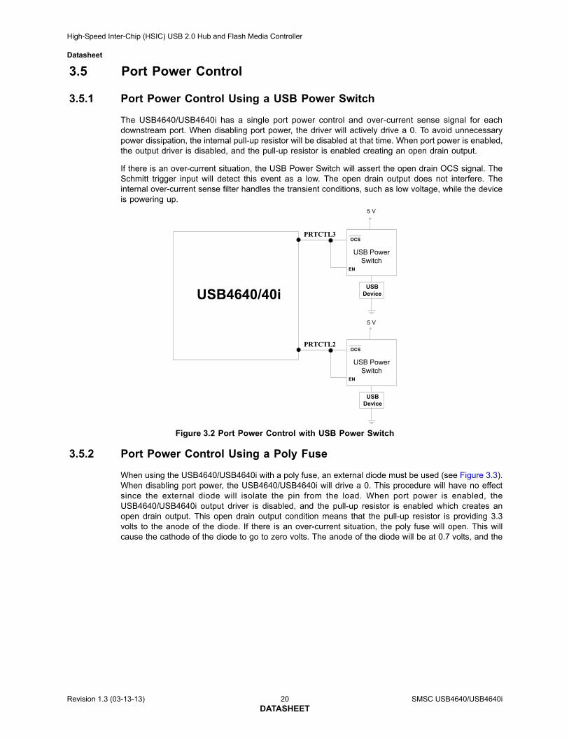
3.5 Port Power Control
3.5.1 Port Power Control Using a USB Power Switch
The USB4640/USB4640i has a single port power control and over-current sense signal for eachdownstream port. When disabling port power, the driver will actively drive a 0. To avoid unnecessarypower dissipation, the internal pull-up resistor will be disabled at that time. When port power is enabled,the output driver is disabled, and the pull-up resistor is enabled creating an open drain output.
If there is an over-current situation, the USB Power Switch will assert the open drain OCS signal. TheSchmitt trigger input will detect this event as a low. The open drain output does not interfere. Theinternal over-current sense filter handles the transient conditions, such as low voltage, while the deviceis powering up.
Figure 3.2 Port Power Control with USB Power Switch
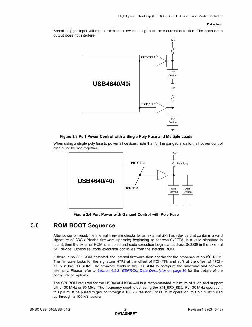
3.5.2 Port Power Control Using a Poly Fuse
When using the USB4640/USB4640i with a poly fuse, an external diode must be used (see Figure 3.3).When disabling port power, the USB4640/USB4640i will drive a 0. This procedure will have no effectsince the external diode will isolate the pin from the load. When port power is enabled, theUSB4640/USB4640i output driver is disabled, and the pull-up resistor is enabled which creates anopen drain output. This open drain output condition means that the pull-up resistor is providing 3.3volts to the anode of the diode. If there is an over-current situation, the poly fuse will open. This willcause the cathode of the diode to go to zero volts. The anode of the diode will be at 0.7 volts, and the
USB Power Switch
5 V
USB Device
PRTCTL3
EN
OCS
USB Power Switch
5 V
USB Device
PRTCTL2
EN
OCS
USB4640/40i
Revision 1.3 (03-13-13) 20 SMSC USB4640/USB4640iDATASHEET
High-Speed Inter-Chip (HSIC) USB 2.0 Hub and Flash Media Controller
Datasheet
Schmitt trigger input will register this as a low resulting in an over-current detection. The open drainoutput does not interfere.
Figure 3.3 Port Power Control with a Single Poly Fuse and Multiple Loads
When using a single poly fuse to power all devices, note that for the ganged situation, all power controlpins must be tied together.
Figure 3.4 Port Power with Ganged Control with Poly Fuse
3.6 ROM BOOT Sequence
After power-on reset, the internal firmware checks for an external SPI flash device that contains a validsignature of 2DFU (device firmware upgrade) beginning at address 0xFFFA. If a valid signature isfound, then the external ROM is enabled and code execution begins at address 0x0000 in the externalSPI device. Otherwise, code execution continues from the internal ROM.
If there is no SPI ROM detected, the internal firmware then checks for the presence of an I2C ROM.The firmware looks for the signature ATA2 at the offset of FCh-FFh and ecf1 at the offset of 17Ch-17Fh in the I2C ROM. The firmware reads in the I2C ROM to configure the hardware and softwareinternally. Please refer to Section 4.3.2: EEPROM Data Descriptor on page 26 for the details of theconfiguration options.
The SPI ROM required for the USB4640/USB4640i is a recommended minimum of 1 Mb and supporteither 30 MHz or 60 MHz. The frequency used is set using the SPI_SPD_SEL. For 30 MHz operation,this pin must be pulled to ground through a 100 kΩ resistor. For 60 MHz operation, this pin must pulledup through a 100 kΩ resistor.
USB4640/40i
USB Device
5 V
PRTCTL3
USB Device
5V
PRTCTL2
USBDevice
Poly Fuse
5 V
USBDevice
PRTCTL2
PRTCTL3
USB4640/40i
SMSC USB4640/USB4640i 21 Revision 1.3 (03-13-13)DATASHEET
High-Speed Inter-Chip (HSIC) USB 2.0 Hub and Flash Media Controller
Datasheet
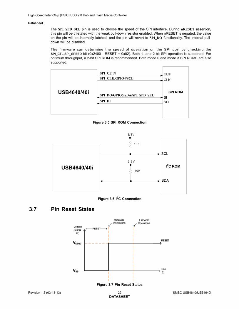
The SPI_SPD_SEL pin is used to choose the speed of the SPI interface. During nRESET assertion,this pin will be tri-stated with the weak pull-down resistor enabled. When nRESET is negated, the valueon the pin will be internally latched, and the pin will revert to SPI_DO functionality. The internal pull-down will be disabled.
The firmware can determine the speed of operation on the SPI port by checking theSPI_CTL.SPI_SPEED bit (0x2400 - RESET = 0x02). Both 1- and 2-bit SPI operation is supported. Foroptimum throughput, a 2-bit SPI ROM is recommended. Both mode 0 and mode 3 SPI ROMS are alsosupported.
Figure 3.5 SPI ROM Connection
Figure 3.6 I2C Connection
3.7 Pin Reset States
Figure 3.7 Pin Reset States
SPI ROM
SPI_CE_N
SPI_CLK/GPIO4/SCL
SPI_DI
SPI_DO/GPIO5/SDA/SPI_SPD_SEL
CE#
CLK
SISO
USB4640/40i
I2C ROM
SCL
SDA
3. 3 V
3. 3 V
10 K
10 KUSB4640/40i
Voltage Signal
(v)
Time (t)
RESET
RESET
Hardware Initialization
FirmwareOperational
VDD33
VSS
Revision 1.3 (03-13-13) 22 SMSC USB4640/USB4640iDATASHEET
High-Speed Inter-Chip (HSIC) USB 2.0 Hub and Flash Media Controller
Datasheet
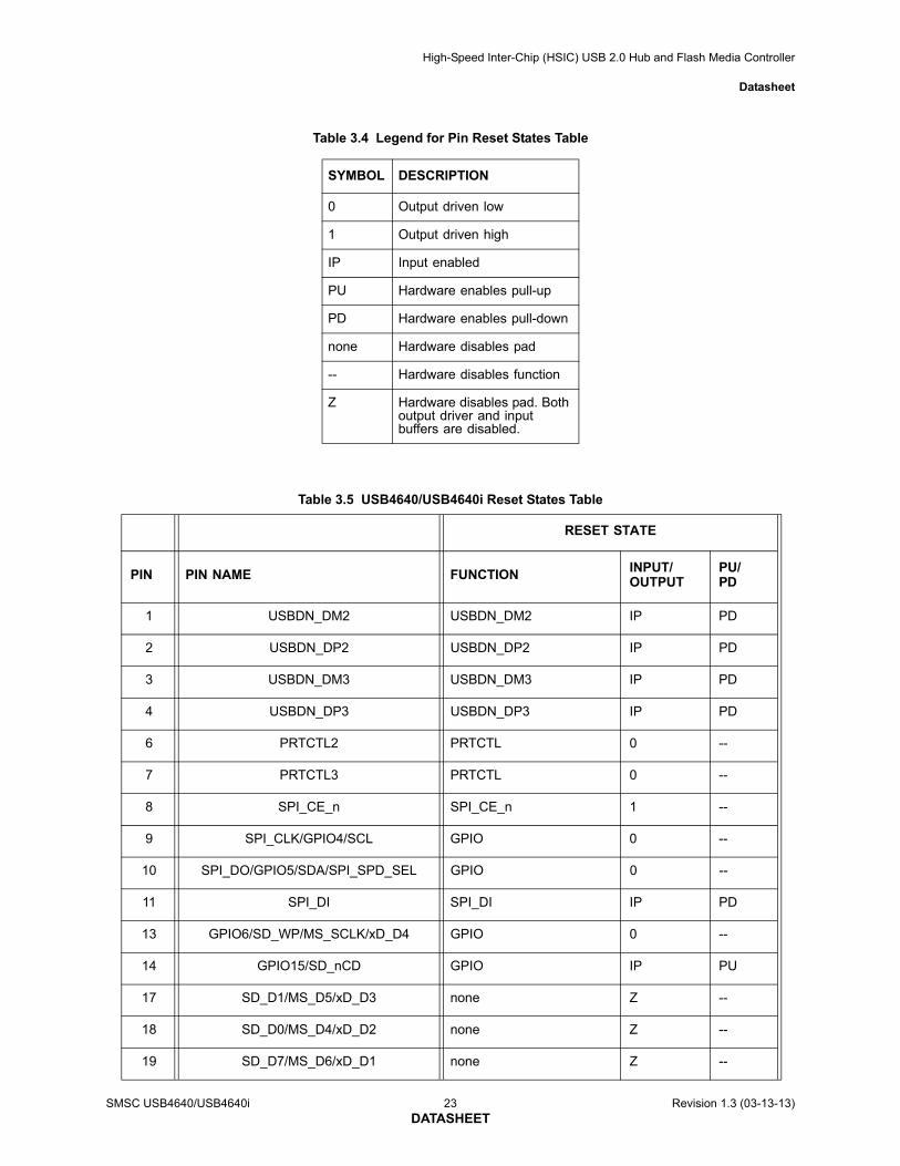
Table 3.4 Legend for Pin Reset States Table
SYMBOL DESCRIPTION
0 Output driven low
1 Output driven high
IP Input enabled
PU Hardware enables pull-up
PD Hardware enables pull-down
none Hardware disables pad
-- Hardware disables function
Z Hardware disables pad. Both output driver and input buffers are disabled.
Table 3.5 USB4640/USB4640i Reset States Table
RESET STATE
PIN PIN NAME FUNCTION INPUT/OUTPUT
PU/PD
1 USBDN_DM2 USBDN_DM2 IP PD
2 USBDN_DP2 USBDN_DP2 IP PD
3 USBDN_DM3 USBDN_DM3 IP PD
4 USBDN_DP3 USBDN_DP3 IP PD
6 PRTCTL2 PRTCTL 0 --
7 PRTCTL3 PRTCTL 0 --
8 SPI_CE_n SPI_CE_n 1 --
9 SPI_CLK/GPIO4/SCL GPIO 0 --
10 SPI_DO/GPIO5/SDA/SPI_SPD_SEL GPIO 0 --
11 SPI_DI SPI_DI IP PD
13 GPIO6/SD_WP/MS_SCLK/xD_D4 GPIO 0 --
14 GPIO15/SD_nCD GPIO IP PU
17 SD_D1/MS_D5/xD_D3 none Z --
18 SD_D0/MS_D4/xD_D2 none Z --
19 SD_D7/MS_D6/xD_D1 none Z --
SMSC USB4640/USB4640i 23 Revision 1.3 (03-13-13)DATASHEET
High-Speed Inter-Chip (HSIC) USB 2.0 Hub and Flash Media Controller
Datasheet
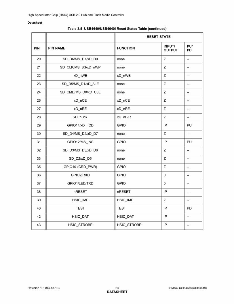
20 SD_D6/MS_D7/xD_D0 none Z --
21 SD_CLK/MS_BS/xD_nWP none Z --
22 xD_nWE xD_nWE Z --
23 SD_D5/MS_D1/xD_ALE none Z --
24 SD_CMD/MS_D0/xD_CLE none Z --
26 xD_nCE xD_nCE Z --
27 xD_nRE xD_nRE Z --
28 xD_nB/R xD_nB/R Z --
29 GPIO14/xD_nCD GPIO IP PU
30 SD_D4/MS_D2/xD_D7 none Z --
31 GPIO12/MS_INS GPIO IP PU
32 SD_D3/MS_D3/xD_D6 none Z --
33 SD_D2/xD_D5 none Z --
35 GPIO10 (CRD_PWR) GPIO Z --
36 GPIO2/RXD GPIO 0 --
37 GPIO1/LED/TXD GPIO 0 --
38 nRESET nRESET IP --
39 HSIC_IMP HSIC_IMP Z --
40 TEST TEST IP PD
42 HSIC_DAT HSIC_DAT IP --
43 HSIC_STROBE HSIC_STROBE IP --
Table 3.5 USB4640/USB4640i Reset States Table (continued)
RESET STATE
PIN PIN NAME FUNCTION INPUT/OUTPUT
PU/PD
Revision 1.3 (03-13-13) 24 SMSC USB4640/USB4640iDATASHEET
High-Speed Inter-Chip (HSIC) USB 2.0 Hub and Flash Media Controller
Datasheet
Chapter 4 Configuration Options
4.1 Hub
SMSC’s USB 2.0 hub is fully compliant to the Universal Serial Bus Specification [1].
The hub provides 1 transaction translator (TT) that is shared by both downstream ports defined as asingle-TT configuration. The TT contains 4 non-periodic buffers. The hub supports a large number offeatures (some are mutually exclusive), and must be configured in order to correctly function whenattached to a USB host controller. There are two principal ways to configure the hub:
Internal default settings
External EEPROM or SPI Flash device
Note: See Chapter 11 (Hub Specification) of the USB specification for general details regarding huboperation and functionality.
4.2 Card Reader
The SMSC USB4640/USB4640i is fully compliant with the following flash media card readerspecifications:
Secure Digital 2.0/MultiMediaCard 4.2
—SD 2.0, HS-SD, HC-SD
—TransFlash™ and reduced form factor media
—1/4/8 bit MMC 4.2
Memory Stick 1.43
Memory Stick Pro Format 1.02
Memory Stick Pro-HG Duo Format 1.01
—Memory Stick, MS Duo, HS-MS, MS Pro-HG, MS Pro
Memory Stick Duo 1.10
xD-Picture Card 1.2
4.3 System Configurations
4.3.1 EEPROM/SPI Interface
The USB4640/USB4640i can be configured via a 2-wire I2C EEPROM (512x8) or an external SPI flashdevice containing the USB4640/USB4640i firmware. If an external configuration device does not existthe internal default values will be used. If one of the external devices is used for configuration, theUSB4640/USB4640i values can be updated through the USB interface. The hub will then attach to theupstream USB host.
The USBDM tool set is available in the USB264x Hub Card reader combo software release package.To download the software package from SMSC's website, visit:
https://www2.smsc.com/mkt/CW_SFT_PUB.nsf/Agreements/OBJ+Hub+Card+Reader
Review the license and select the I agree checkbox, followed by the Confirm button. Download theUSB264x Hub Card reader combo Release Package zip file with the USBDM tool set will then beavailable for download.
SMSC USB4640/USB4640i 25 Revision 1.3 (03-13-13)DATASHEET
High-Speed Inter-Chip (HSIC) USB 2.0 Hub and Flash Media Controller
Datasheet
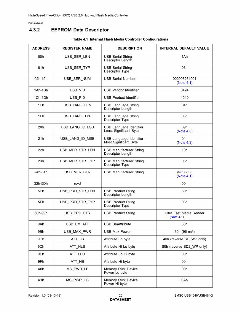
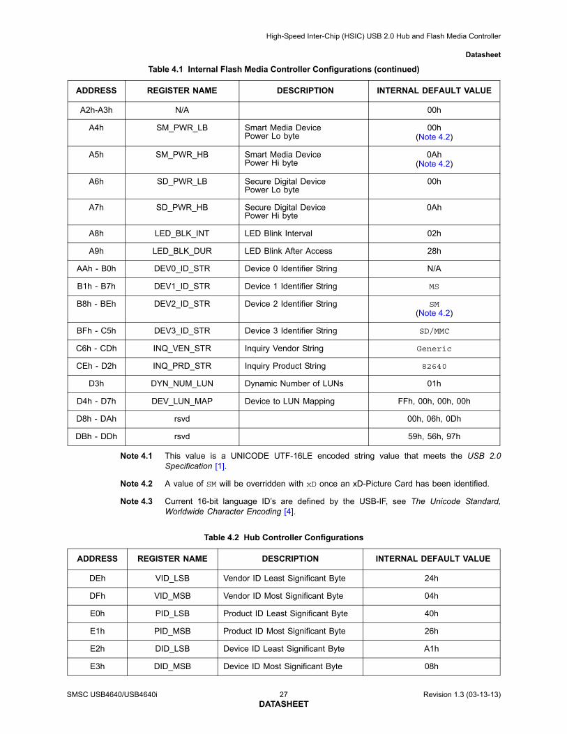
4.3.2 EEPROM Data Descriptor
Table 4.1 Internal Flash Media Controller Configurations
ADDRESS REGISTER NAME DESCRIPTION INTERNAL DEFAULT VALUE
00h USB_SER_LEN USB Serial StringDescriptor Length
1Ah
01h USB_SER_TYP USB Serial StringDescriptor Type
03h
02h-19h USB_SER_NUM USB Serial Number 000008264001(Note 4.1)
1Ah-1Bh USB_VID USB Vendor Identifier 0424
1Ch-1Dh USB_PID USB Product Identifier 4040
1Eh USB_LANG_LEN USB Language String Descriptor Length
04h
1Fh USB_LANG_TYP USB Language String Descriptor Type
03h
20h USB_LANG_ID_LSB USB Language IdentifierLeast Significant Byte
09h(Note 4.3)
21h USB_LANG_ID_MSB USB Language IdentifierMost Significant Byte
04h(Note 4.3)
22h USB_MFR_STR_LEN USB Manufacturer StringDescriptor Length
10h
23h USB_MFR_STR_TYP USB Manufacturer String Descriptor Type
03h
24h-31h USB_MFR_STR USB Manufacturer String Generic(Note 4.1)
32h-5Dh rsvd 00h
5Eh USB_PRD_STR_LEN USB Product StringDescriptor Length
30h
5Fh USB_PRD_STR_TYP USB Product StringDescriptor Type
03h
60h-99h USB_PRD_STR USB Product String Ultra Fast Media Reader— (Note 4.1)
9Ah USB_BM_ATT USB BmAttribute 80h
9Bh USB_MAX_PWR USB Max Power 30h (96 mA)
9Ch ATT_LB Attribute Lo byte 40h (reverse SD_WP only)
9Dh ATT_HLB Attribute Hi Lo byte 80h (reverse SD2_WP only)
9Eh ATT_LHB Attribute Lo Hi byte 00h
9Fh ATT_HB Attribute Hi byte 00h
A0h MS_PWR_LB Memory Stick DevicePower Lo byte
00h
A1h MS_PWR_HB Memory Stick DevicePower Hi byte
0Ah
Revision 1.3 (03-13-13) 26 SMSC USB4640/USB4640iDATASHEET
High-Speed Inter-Chip (HSIC) USB 2.0 Hub and Flash Media Controller
Datasheet
Note 4.1 This value is a UNICODE UTF-16LE encoded string value that meets the USB 2.0Specification [1].
Note 4.2 A value of SM will be overridden with xD once an xD-Picture Card has been identified.
Note 4.3 Current 16-bit language ID’s are defined by the USB-IF, see The Unicode Standard,Worldwide Character Encoding [4].
A2h-A3h N/A 00h
A4h SM_PWR_LB Smart Media DevicePower Lo byte
00h(Note 4.2)
A5h SM_PWR_HB Smart Media DevicePower Hi byte
0Ah(Note 4.2)
A6h SD_PWR_LB Secure Digital DevicePower Lo byte
00h
A7h SD_PWR_HB Secure Digital DevicePower Hi byte
0Ah
A8h LED_BLK_INT LED Blink Interval 02h
A9h LED_BLK_DUR LED Blink After Access 28h
AAh - B0h DEV0_ID_STR Device 0 Identifier String N/A
B1h - B7h DEV1_ID_STR Device 1 Identifier String MS
B8h - BEh DEV2_ID_STR Device 2 Identifier String SM(Note 4.2)
BFh - C5h DEV3_ID_STR Device 3 Identifier String SD/MMC
C6h - CDh INQ_VEN_STR Inquiry Vendor String Generic
CEh - D2h INQ_PRD_STR Inquiry Product String 82640
D3h DYN_NUM_LUN Dynamic Number of LUNs 01h
D4h - D7h DEV_LUN_MAP Device to LUN Mapping FFh, 00h, 00h, 00h
D8h - DAh rsvd 00h, 06h, 0Dh
DBh - DDh rsvd 59h, 56h, 97h
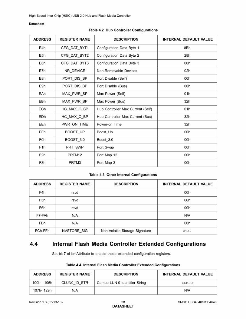
Table 4.2 Hub Controller Configurations
ADDRESS REGISTER NAME DESCRIPTION INTERNAL DEFAULT VALUE
DEh VID_LSB Vendor ID Least Significant Byte 24h
DFh VID_MSB Vendor ID Most Significant Byte 04h
E0h PID_LSB Product ID Least Significant Byte 40h
E1h PID_MSB Product ID Most Significant Byte 26h
E2h DID_LSB Device ID Least Significant Byte A1h
E3h DID_MSB Device ID Most Significant Byte 08h
Table 4.1 Internal Flash Media Controller Configurations (continued)
ADDRESS REGISTER NAME DESCRIPTION INTERNAL DEFAULT VALUE
SMSC USB4640/USB4640i 27 Revision 1.3 (03-13-13)DATASHEET
High-Speed Inter-Chip (HSIC) USB 2.0 Hub and Flash Media Controller
Datasheet
4.4 Internal Flash Media Controller Extended Configurations
Set bit 7 of bmAttribute to enable these extended configuration registers.
E4h CFG_DAT_BYT1 Configuration Data Byte 1 8Bh
E5h CFG_DAT_BYT2 Configuration Data Byte 2 28h
E6h CFG_DAT_BYT3 Configuration Data Byte 3 00h
E7h NR_DEVICE Non-Removable Devices 02h
E8h PORT_DIS_SP Port Disable (Self) 00h
E9h PORT_DIS_BP Port Disable (Bus) 00h
EAh MAX_PWR_SP Max Power (Self) 01h
EBh MAX_PWR_BP Max Power (Bus) 32h
ECh HC_MAX_C_SP Hub Controller Max Current (Self) 01h
EDh HC_MAX_C_BP Hub Controller Max Current (Bus) 32h
EEh PWR_ON_TIME Power-on Time 32h
EFh BOOST_UP Boost_Up 00h
F0h BOOST_3:0 Boost_3:0 00h
F1h PRT_SWP Port Swap 00h
F2h PRTM12 Port Map 12 00h
F3h PRTM3 Port Map 3 00h
Table 4.3 Other Internal Configurations
ADDRESS REGISTER NAME DESCRIPTION INTERNAL DEFAULT VALUE
F4h rsvd 00h
F5h rsvd 66h
F6h rsvd 00h
F7-FAh N/A N/A
FBh N/A 00h
FCh-FFh NVSTORE_SIG Non-Volatile Storage Signature ATA2
Table 4.4 Internal Flash Media Controller Extended Configurations
ADDRESS REGISTER NAME DESCRIPTION INTERNAL DEFAULT VALUE
100h - 106h CLUN0_ID_STR Combo LUN 0 Identifier String COMBO
107h- 129h N/A N/A
Table 4.2 Hub Controller Configurations
ADDRESS REGISTER NAME DESCRIPTION INTERNAL DEFAULT VALUE
Revision 1.3 (03-13-13) 28 SMSC USB4640/USB4640iDATASHEET
High-Speed Inter-Chip (HSIC) USB 2.0 Hub and Flash Media Controller
Datasheet
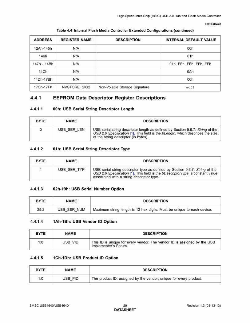
4.4.1 EEPROM Data Descriptor Register Descriptions
4.4.1.1 00h: USB Serial String Descriptor Length
4.4.1.2 01h: USB Serial String Descriptor Type
4.4.1.3 02h-19h: USB Serial Number Option
4.4.1.4 1Ah-1Bh: USB Vendor ID Option
4.4.1.5 1Ch-1Dh: USB Product ID Option
12Ah-145h N/A 00h
146h N/A 01h
147h - 14Bh N/A 01h, FFh, FFh, FFh, FFh
14Ch N/A 0Ah
14Dh-17Bh N/A 00h
17Ch-17Fh NVSTORE_SIG2 Non-Volatile Storage Signature ecf1
BYTE NAME DESCRIPTION
0 USB_SER_LEN USB serial string descriptor length as defined by Section 9.6.7: String of the USB 2.0 Specification [1]. This field is the bLength, which describes the size of the string descriptor (in bytes).
BYTE NAME DESCRIPTION
1 USB_SER_TYP USB serial string descriptor type as defined by Section 9.6.7: String of the USB 2.0 Specification [1]. This field is the bDescriptorType, a constant value associated with a string descriptor type.
BYTE NAME DESCRIPTION
25:2 USB_SER_NUM Maximum string length is 12 hex digits. Must be unique to each device.
BYTE NAME DESCRIPTION
1:0 USB_VID This ID is unique for every vendor. The vendor ID is assigned by the USB Implementer’s Forum.
BYTE NAME DESCRIPTION
1:0 USB_PID The product ID: assigned by the vendor; unique for every product.
Table 4.4 Internal Flash Media Controller Extended Configurations (continued)
ADDRESS REGISTER NAME DESCRIPTION INTERNAL DEFAULT VALUE
SMSC USB4640/USB4640i 29 Revision 1.3 (03-13-13)DATASHEET
High-Speed Inter-Chip (HSIC) USB 2.0 Hub and Flash Media Controller
Datasheet
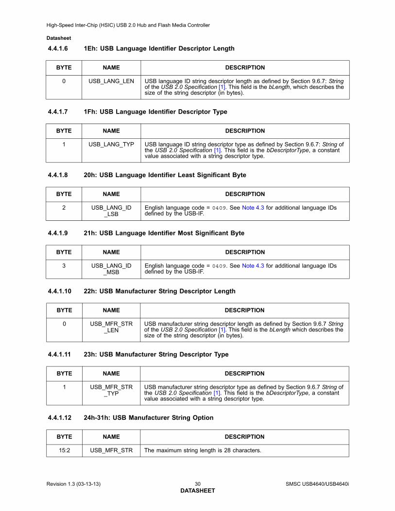
4.4.1.6 1Eh: USB Language Identifier Descriptor Length
4.4.1.7 1Fh: USB Language Identifier Descriptor Type
4.4.1.8 20h: USB Language Identifier Least Significant Byte
4.4.1.9 21h: USB Language Identifier Most Significant Byte
4.4.1.10 22h: USB Manufacturer String Descriptor Length
4.4.1.11 23h: USB Manufacturer String Descriptor Type
4.4.1.12 24h-31h: USB Manufacturer String Option
BYTE NAME DESCRIPTION
0 USB_LANG_LEN USB language ID string descriptor length as defined by Section 9.6.7: String of the USB 2.0 Specification [1]. This field is the bLength, which describes the size of the string descriptor (in bytes).
BYTE NAME DESCRIPTION
1 USB_LANG_TYP USB language ID string descriptor type as defined by Section 9.6.7: String of the USB 2.0 Specification [1]. This field is the bDescriptorType, a constant value associated with a string descriptor type.
BYTE NAME DESCRIPTION
2 USB_LANG_ID_LSB
English language code = 0409. See Note 4.3 for additional language IDs defined by the USB-IF.
BYTE NAME DESCRIPTION
3 USB_LANG_ID_MSB
English language code = 0409. See Note 4.3 for additional language IDs defined by the USB-IF.
BYTE NAME DESCRIPTION
0 USB_MFR_STR_LEN
USB manufacturer string descriptor length as defined by Section 9.6.7 String of the USB 2.0 Specification [1]. This field is the bLength which describes the size of the string descriptor (in bytes).
BYTE NAME DESCRIPTION
1 USB_MFR_STR_TYP
USB manufacturer string descriptor type as defined by Section 9.6.7 String of the USB 2.0 Specification [1]. This field is the bDescriptorType, a constant value associated with a string descriptor type.
BYTE NAME DESCRIPTION
15:2 USB_MFR_STR The maximum string length is 28 characters.
Revision 1.3 (03-13-13) 30 SMSC USB4640/USB4640iDATASHEET
High-Speed Inter-Chip (HSIC) USB 2.0 Hub and Flash Media Controller
Datasheet
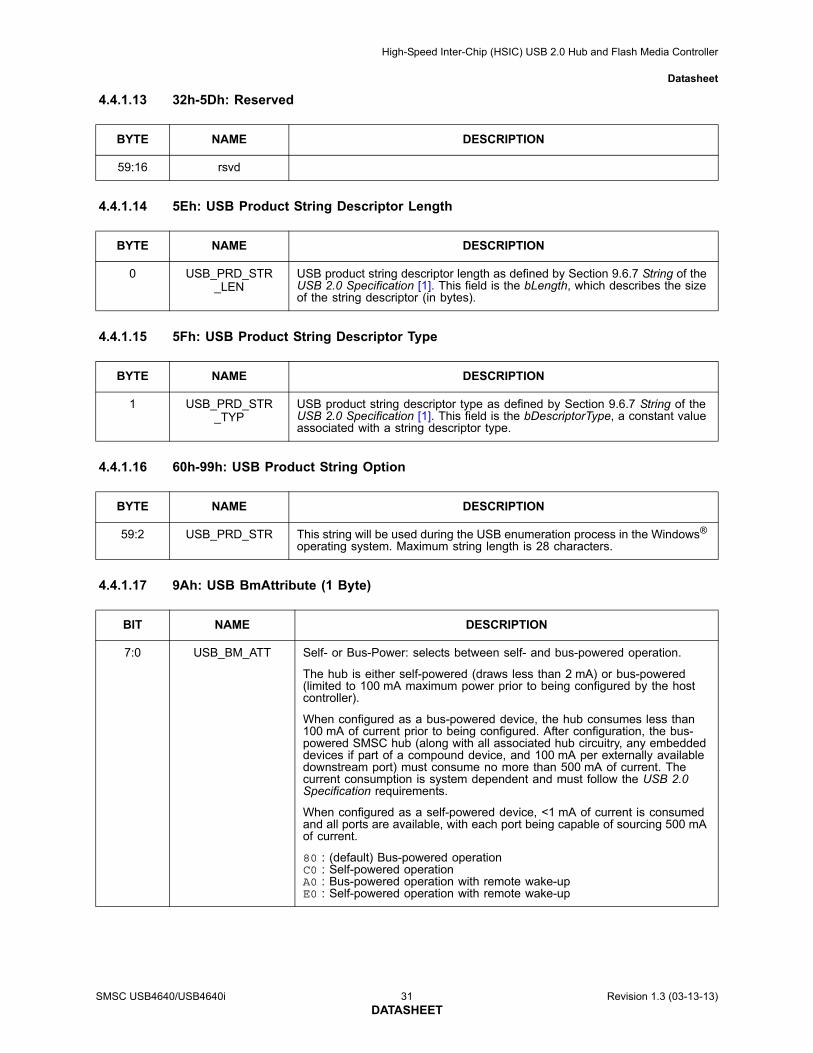
4.4.1.13 32h-5Dh: Reserved
4.4.1.14 5Eh: USB Product String Descriptor Length
4.4.1.15 5Fh: USB Product String Descriptor Type
4.4.1.16 60h-99h: USB Product String Option
4.4.1.17 9Ah: USB BmAttribute (1 Byte)
BYTE NAME DESCRIPTION
59:16 rsvd
BYTE NAME DESCRIPTION
0 USB_PRD_STR_LEN
USB product string descriptor length as defined by Section 9.6.7 String of the USB 2.0 Specification [1]. This field is the bLength, which describes the size of the string descriptor (in bytes).
BYTE NAME DESCRIPTION
1 USB_PRD_STR_TYP
USB product string descriptor type as defined by Section 9.6.7 String of the USB 2.0 Specification [1]. This field is the bDescriptorType, a constant value associated with a string descriptor type.
BYTE NAME DESCRIPTION
59:2 USB_PRD_STR This string will be used during the USB enumeration process in the Windows® operating system. Maximum string length is 28 characters.
BIT NAME DESCRIPTION
7:0 USB_BM_ATT Self- or Bus-Power: selects between self- and bus-powered operation.
The hub is either self-powered (draws less than 2 mA) or bus-powered (limited to 100 mA maximum power prior to being configured by the host controller).
When configured as a bus-powered device, the hub consumes less than 100 mA of current prior to being configured. After configuration, the bus-powered SMSC hub (along with all associated hub circuitry, any embedded devices if part of a compound device, and 100 mA per externally available downstream port) must consume no more than 500 mA of current. The current consumption is system dependent and must follow the USB 2.0 Specification requirements.
When configured as a self-powered device, <1 mA of current is consumed and all ports are available, with each port being capable of sourcing 500 mA of current.
80 : (default) Bus-powered operationC0 : Self-powered operationA0 : Bus-powered operation with remote wake-upE0 : Self-powered operation with remote wake-up
SMSC USB4640/USB4640i 31 Revision 1.3 (03-13-13)DATASHEET
High-Speed Inter-Chip (HSIC) USB 2.0 Hub and Flash Media Controller
Datasheet
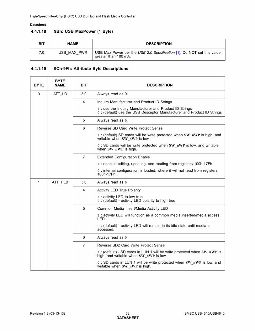
4.4.1.18 9Bh: USB MaxPower (1 Byte)
4.4.1.19 9Ch-9Fh: Attribute Byte Descriptions
BIT NAME DESCRIPTION
7:0 USB_MAX_PWR USB Max Power per the USB 2.0 Specification [1]. Do NOT set this value greater than 100 mA.
BYTEBYTE NAME BIT DESCRIPTION
0 ATT_LB 3:0 Always read as 0
4 Inquire Manufacturer and Product ID Strings
1 : use the Inquiry Manufacturer and Product ID Strings0 : (default) use the USB Descriptor Manufacturer and Product ID Strings
5 Always read as 0
6 Reverse SD Card Write Protect Sense
1 : (default) SD cards will be write protected when SW_nWP is high, and writable when SW_nWP is low.
0 : SD cards will be write protected when SW_nWP is low, and writable when SW_nWP is high.
7 Extended Configuration Enable
1 : enables editing, updating, and reading from registers 100h-17Fh.
0 : internal configuration is loaded, where it will not read from registers 100h-17Fh.
1 ATT_HLB 3:0 Always read as 0
4 Activity LED True Polarity
1 : activity LED to low true0 : (default) - activity LED polarity to high true
5 Common Media Insert/Media Activity LED
1 : activity LED will function as a common media inserted/media access LED.
0 : (default) - activity LED will remain in its idle state until media is accessed.
6 Always read as 0
7 Reverse SD2 Card Write Protect Sense
1 : (default) - SD cards in LUN 1 will be write protected when SW_nWP is high, and writable when SW_nWP is low.
0 : SD cards in LUN 1 will be write protected when SW_nWP is low, and writable when SW_nWP is high.
Revision 1.3 (03-13-13) 32 SMSC USB4640/USB4640iDATASHEET
High-Speed Inter-Chip (HSIC) USB 2.0 Hub and Flash Media Controller
Datasheet
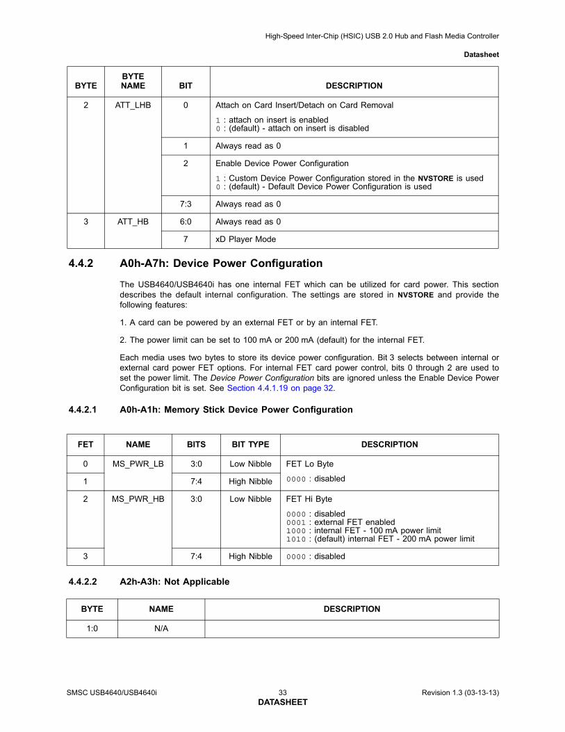
4.4.2 A0h-A7h: Device Power Configuration
The USB4640/USB4640i has one internal FET which can be utilized for card power. This sectiondescribes the default internal configuration. The settings are stored in NVSTORE and provide thefollowing features:
1. A card can be powered by an external FET or by an internal FET.
2. The power limit can be set to 100 mA or 200 mA (default) for the internal FET.
Each media uses two bytes to store its device power configuration. Bit 3 selects between internal orexternal card power FET options. For internal FET card power control, bits 0 through 2 are used toset the power limit. The Device Power Configuration bits are ignored unless the Enable Device PowerConfiguration bit is set. See Section 4.4.1.19 on page 32.
4.4.2.1 A0h-A1h: Memory Stick Device Power Configuration
4.4.2.2 A2h-A3h: Not Applicable
2 ATT_LHB 0 Attach on Card Insert/Detach on Card Removal
1 : attach on insert is enabled0 : (default) - attach on insert is disabled
1 Always read as 0
2 Enable Device Power Configuration
1 : Custom Device Power Configuration stored in the NVSTORE is used0 : (default) - Default Device Power Configuration is used
7:3 Always read as 0
3 ATT_HB 6:0 Always read as 0
7 xD Player Mode
FET NAME BITS BIT TYPE DESCRIPTION
0 MS_PWR_LB 3:0 Low Nibble FET Lo Byte
0000 : disabled1 7:4 High Nibble
2 MS_PWR_HB 3:0 Low Nibble FET Hi Byte
0000 : disabled0001 : external FET enabled1000 : internal FET - 100 mA power limit1010 : (default) internal FET - 200 mA power limit
3 7:4 High Nibble 0000 : disabled
BYTE NAME DESCRIPTION
1:0 N/A
BYTEBYTE NAME BIT DESCRIPTION
SMSC USB4640/USB4640i 33 Revision 1.3 (03-13-13)DATASHEET
High-Speed Inter-Chip (HSIC) USB 2.0 Hub and Flash Media Controller
Datasheet
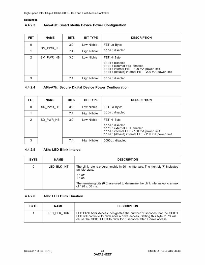
4.4.2.3 A4h-A5h: Smart Media Device Power Configuration
4.4.2.4 A6h-A7h: Secure Digital Device Power Configuration
4.4.2.5 A8h: LED Blink Interval
4.4.2.6 A9h: LED Blink Duration
FET NAME BITS BIT TYPE DESCRIPTION
0SM_PWR_LB
3:0 Low Nibble FET Lo Byte:
0000 : disabled1 7:4 High Nibble
2 SM_PWR_HB 3:0 Low Nibble FET Hi Byte
0000 : disabled0001 : external FET enabled1000 : internal FET - 100 mA power limit1010 : (default) internal FET - 200 mA power limit
3 7:4 High Nibble 0000 : disabled
FET NAME BITS BIT TYPE DESCRIPTION
0 SD_PWR_LB 3:0 Low Nibble FET Lo Byte:
0000 : disabled1 7:4 High Nibble
2 SD_PWR_HB 3:0 Low Nibble FET Hi Byte
0000 : disabled0001 : external FET enabled1000 : internal FET - 100 mA power limit1010 : (default) internal FET - 200 mA power limit
3 7:4 High Nibble 0000b : disabled
BYTE NAME DESCRIPTION
0 LED_BLK_INT The blink rate is programmable in 50 ms intervals. The high bit (7) indicates an idle state:
0 : off1 : on
The remaining bits (6:0) are used to determine the blink interval up to a max of 128 x 50 ms.
BYTE NAME DESCRIPTION
1 LED_BLK_DUR LED Blink After Access: designates the number of seconds that the GPIO1 LED will continue to blink after a drive access. Setting this byte to 05 will cause the GPIO 1 LED to blink for 5 seconds after a drive access.
Revision 1.3 (03-13-13) 34 SMSC USB4640/USB4640iDATASHEET
High-Speed Inter-Chip (HSIC) USB 2.0 Hub and Flash Media Controller
Datasheet
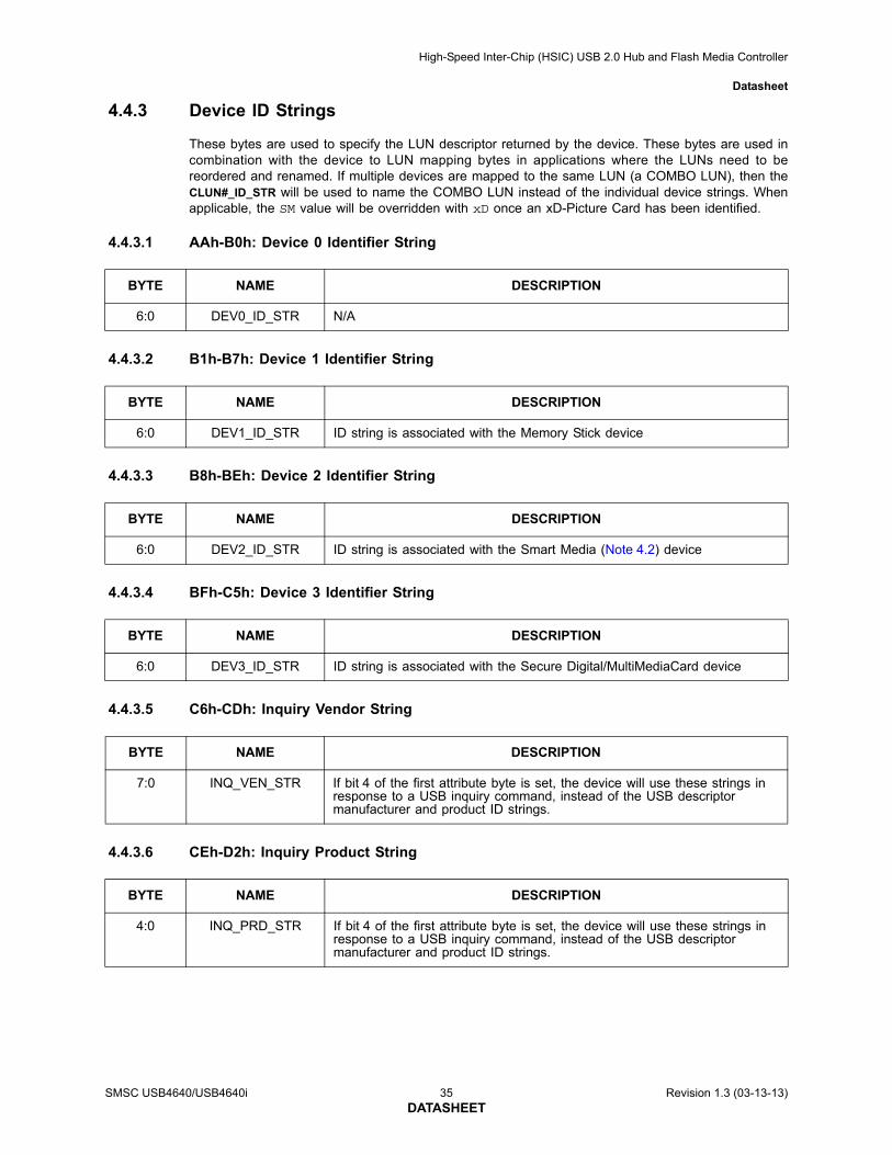
4.4.3 Device ID Strings
These bytes are used to specify the LUN descriptor returned by the device. These bytes are used incombination with the device to LUN mapping bytes in applications where the LUNs need to bereordered and renamed. If multiple devices are mapped to the same LUN (a COMBO LUN), then theCLUN#_ID_STR will be used to name the COMBO LUN instead of the individual device strings. Whenapplicable, the SM value will be overridden with xD once an xD-Picture Card has been identified.
4.4.3.1 AAh-B0h: Device 0 Identifier String
4.4.3.2 B1h-B7h: Device 1 Identifier String
4.4.3.3 B8h-BEh: Device 2 Identifier String
4.4.3.4 BFh-C5h: Device 3 Identifier String
4.4.3.5 C6h-CDh: Inquiry Vendor String
4.4.3.6 CEh-D2h: Inquiry Product String
BYTE NAME DESCRIPTION
6:0 DEV0_ID_STR N/A
BYTE NAME DESCRIPTION
6:0 DEV1_ID_STR ID string is associated with the Memory Stick device
BYTE NAME DESCRIPTION
6:0 DEV2_ID_STR ID string is associated with the Smart Media (Note 4.2) device
BYTE NAME DESCRIPTION
6:0 DEV3_ID_STR ID string is associated with the Secure Digital/MultiMediaCard device
BYTE NAME DESCRIPTION
7:0 INQ_VEN_STR If bit 4 of the first attribute byte is set, the device will use these strings in response to a USB inquiry command, instead of the USB descriptor manufacturer and product ID strings.
BYTE NAME DESCRIPTION
4:0 INQ_PRD_STR If bit 4 of the first attribute byte is set, the device will use these strings in response to a USB inquiry command, instead of the USB descriptor manufacturer and product ID strings.
SMSC USB4640/USB4640i 35 Revision 1.3 (03-13-13)DATASHEET
High-Speed Inter-Chip (HSIC) USB 2.0 Hub and Flash Media Controller
Datasheet
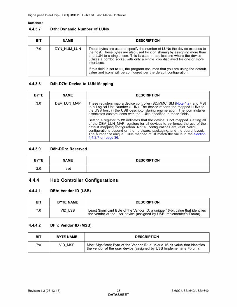
4.4.3.7 D3h: Dynamic Number of LUNs
4.4.3.8 D4h-D7h: Device to LUN Mapping
4.4.3.9 D8h-DDh: Reserved
4.4.4 Hub Controller Configurations
4.4.4.1 DEh: Vendor ID (LSB)
4.4.4.2 DFh: Vendor ID (MSB)
BIT NAME DESCRIPTION
7:0 DYN_NUM_LUN These bytes are used to specify the number of LUNs the device exposes to the host. These bytes are also used for icon sharing by assigning more than one LUN to a single icon. This is used in applications where the device utilizes a combo socket with only a single icon displayed for one or more interfaces.
If this field is set to FF, the program assumes that you are using the default value and icons will be configured per the default configuration.
BYTE NAME DESCRIPTION
3:0 DEV_LUN_MAP These registers map a device controller (SD/MMC, SM (Note 4.2), and MS) to a Logical Unit Number (LUN). The device reports the mapped LUNs to the USB host in the USB descriptor during enumeration. The icon installer associates custom icons with the LUNs specified in these fields.
Setting a register to FF indicates that the device is not mapped. Setting all of the DEV_LUN_MAP registers for all devices to FF forces the use of the default mapping configuration. Not all configurations are valid. Valid configurations depend on the hardware, packaging, and the board layout. The number of unique LUNs mapped must match the value in the Section 4.4.3.7 on page 36.
BYTE NAME DESCRIPTION
2:0 rsvd
BIT BYTE NAME DESCRIPTION
7:0 VID_LSB Least Significant Byte of the Vendor ID: a unique 16-bit value that identifies the vendor of the user device (assigned by USB Implementer’s Forum).
BIT BYTE NAME DESCRIPTION
7:0 VID_MSB Most Significant Byte of the Vendor ID: a unique 16-bit value that identifies the vendor of the user device (assigned by USB Implementer’s Forum).
Revision 1.3 (03-13-13) 36 SMSC USB4640/USB4640iDATASHEET
High-Speed Inter-Chip (HSIC) USB 2.0 Hub and Flash Media Controller
Datasheet
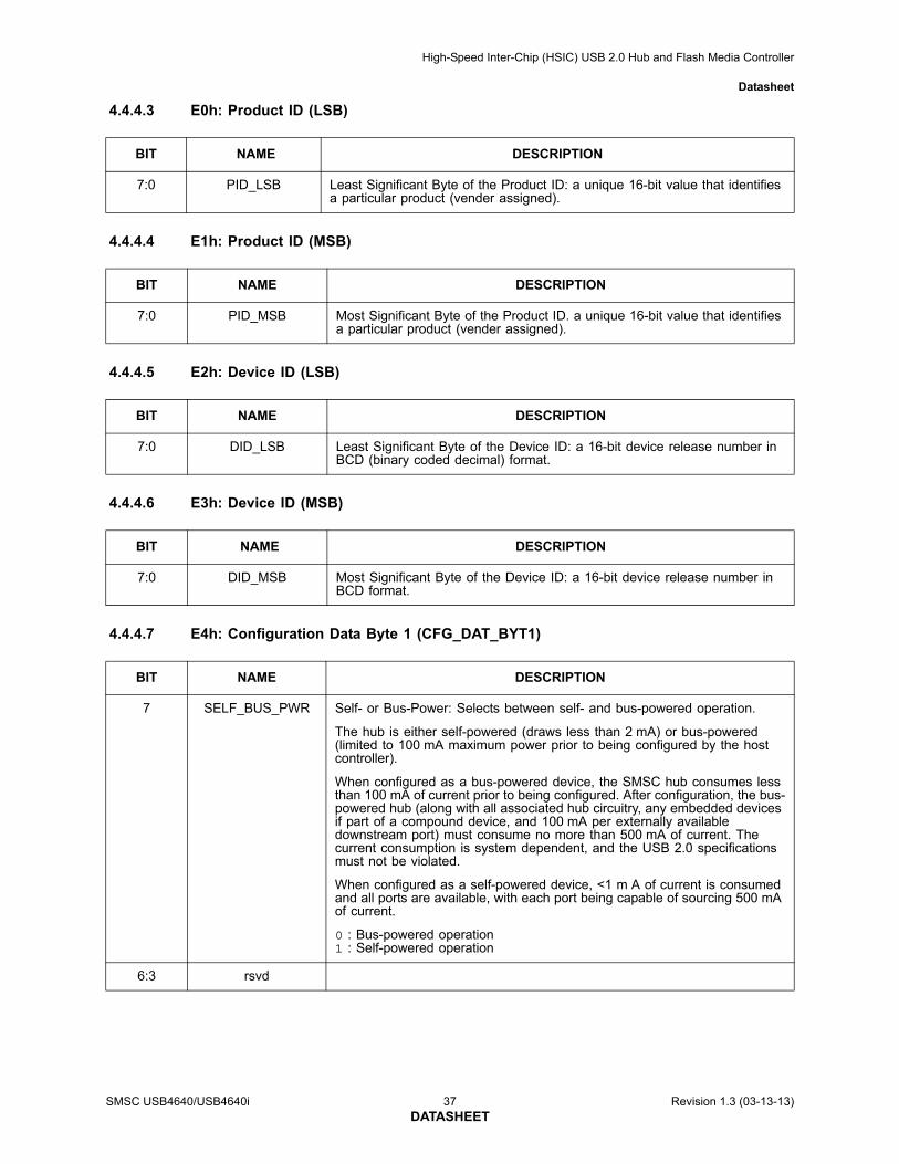
4.4.4.3 E0h: Product ID (LSB)
4.4.4.4 E1h: Product ID (MSB)
4.4.4.5 E2h: Device ID (LSB)
4.4.4.6 E3h: Device ID (MSB)
4.4.4.7 E4h: Configuration Data Byte 1 (CFG_DAT_BYT1)
BIT NAME DESCRIPTION
7:0 PID_LSB Least Significant Byte of the Product ID: a unique 16-bit value that identifies a particular product (vender assigned).
BIT NAME DESCRIPTION
7:0 PID_MSB Most Significant Byte of the Product ID. a unique 16-bit value that identifies a particular product (vender assigned).
BIT NAME DESCRIPTION
7:0 DID_LSB Least Significant Byte of the Device ID: a 16-bit device release number in BCD (binary coded decimal) format.
BIT NAME DESCRIPTION
7:0 DID_MSB Most Significant Byte of the Device ID: a 16-bit device release number in BCD format.
BIT NAME DESCRIPTION
7 SELF_BUS_PWR Self- or Bus-Power: Selects between self- and bus-powered operation.
The hub is either self-powered (draws less than 2 mA) or bus-powered (limited to 100 mA maximum power prior to being configured by the host controller).
When configured as a bus-powered device, the SMSC hub consumes less than 100 mA of current prior to being configured. After configuration, the bus-powered hub (along with all associated hub circuitry, any embedded devices if part of a compound device, and 100 mA per externally available downstream port) must consume no more than 500 mA of current. The current consumption is system dependent, and the USB 2.0 specifications must not be violated.
When configured as a self-powered device, <1 m A of current is consumed and all ports are available, with each port being capable of sourcing 500 mA of current.
0 : Bus-powered operation1 : Self-powered operation
6:3 rsvd
SMSC USB4640/USB4640i 37 Revision 1.3 (03-13-13)DATASHEET
High-Speed Inter-Chip (HSIC) USB 2.0 Hub and Flash Media Controller
Datasheet
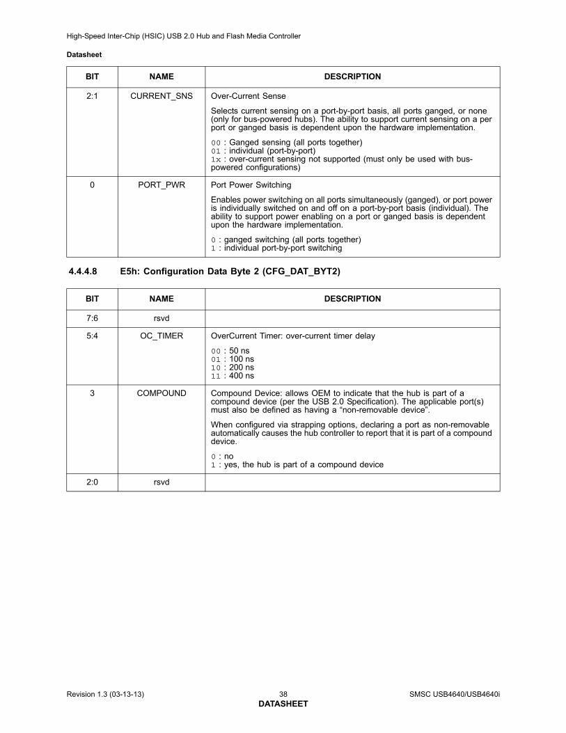
4.4.4.8 E5h: Configuration Data Byte 2 (CFG_DAT_BYT2)
2:1 CURRENT_SNS Over-Current Sense
Selects current sensing on a port-by-port basis, all ports ganged, or none (only for bus-powered hubs). The ability to support current sensing on a per port or ganged basis is dependent upon the hardware implementation.
00 : Ganged sensing (all ports together)01 : individual (port-by-port)1x : over-current sensing not supported (must only be used with bus-powered configurations)
0 PORT_PWR Port Power Switching
Enables power switching on all ports simultaneously (ganged), or port power is individually switched on and off on a port-by-port basis (individual). The ability to support power enabling on a port or ganged basis is dependent upon the hardware implementation.
0 : ganged switching (all ports together)1 : individual port-by-port switching
BIT NAME DESCRIPTION
7:6 rsvd
5:4 OC_TIMER OverCurrent Timer: over-current timer delay
00 : 50 ns01 : 100 ns10 : 200 ns11 : 400 ns
3 COMPOUND Compound Device: allows OEM to indicate that the hub is part of a compound device (per the USB 2.0 Specification). The applicable port(s) must also be defined as having a “non-removable device”.
When configured via strapping options, declaring a port as non-removable automatically causes the hub controller to report that it is part of a compound device.
0 : no1 : yes, the hub is part of a compound device
2:0 rsvd
BIT NAME DESCRIPTION
Revision 1.3 (03-13-13) 38 SMSC USB4640/USB4640iDATASHEET
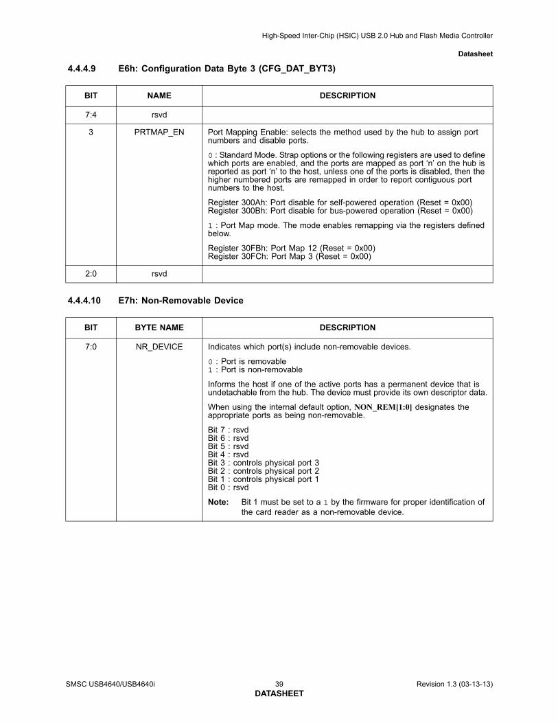
High-Speed Inter-Chip (HSIC) USB 2.0 Hub and Flash Media Controller
Datasheet
4.4.4.9 E6h: Configuration Data Byte 3 (CFG_DAT_BYT3)
4.4.4.10 E7h: Non-Removable Device
BIT NAME DESCRIPTION
7:4 rsvd
3 PRTMAP_EN Port Mapping Enable: selects the method used by the hub to assign port numbers and disable ports.
0 : Standard Mode. Strap options or the following registers are used to define which ports are enabled, and the ports are mapped as port ‘n’ on the hub is reported as port ‘n’ to the host, unless one of the ports is disabled, then the higher numbered ports are remapped in order to report contiguous port numbers to the host.
Register 300Ah: Port disable for self-powered operation (Reset = 0x00)Register 300Bh: Port disable for bus-powered operation (Reset = 0x00)
1 : Port Map mode. The mode enables remapping via the registers defined below.
Register 30FBh: Port Map 12 (Reset = 0x00)Register 30FCh: Port Map 3 (Reset = 0x00)
2:0 rsvd
BIT BYTE NAME DESCRIPTION
7:0 NR_DEVICE Indicates which port(s) include non-removable devices.
0 : Port is removable1 : Port is non-removable
Informs the host if one of the active ports has a permanent device that is undetachable from the hub. The device must provide its own descriptor data.
When using the internal default option, NON_REM[1:0] designates the appropriate ports as being non-removable.
Bit 7 : rsvdBit 6 : rsvdBit 5 : rsvdBit 4 : rsvdBit 3 : controls physical port 3Bit 2 : controls physical port 2Bit 1 : controls physical port 1Bit 0 : rsvd
Note: Bit 1 must be set to a 1 by the firmware for proper identification of the card reader as a non-removable device.
SMSC USB4640/USB4640i 39 Revision 1.3 (03-13-13)DATASHEET
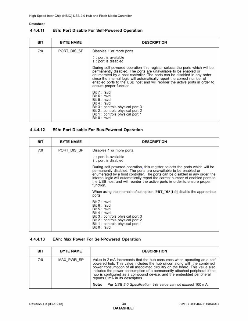
High-Speed Inter-Chip (HSIC) USB 2.0 Hub and Flash Media Controller
Datasheet
4.4.4.11 E8h: Port Disable For Self-Powered Operation
4.4.4.12 E9h: Port Disable For Bus-Powered Operation
4.4.4.13 EAh: Max Power For Self-Powered Operation
BIT BYTE NAME DESCRIPTION
7:0 PORT_DIS_SP Disables 1 or more ports.
0 : port is available1 : port is disabled
During self-powered operation this register selects the ports which will be permanently disabled. The ports are unavailable to be enabled or enumerated by a host controller. The ports can be disabled in any order since the internal logic will automatically report the correct number of enabled ports to the USB host and will reorder the active ports in order to ensure proper function.
Bit 7 : rsvdBit 6 : rsvdBit 5 : rsvdBit 4 : rsvdBit 3 : controls physical port 3Bit 2 : controls physical port 2Bit 1 : controls physical port 1Bit 0 : rsvd
BIT BYTE NAME DESCRIPTION
7:0 PORT_DIS_BP Disables 1 or more ports.
0 : port is available1 : port is disabled
During self-powered operation, this register selects the ports which will be permanently disabled. The ports are unavailable to be enabled or enumerated by a host controller. The ports can be disabled in any order, the internal logic will automatically report the correct number of enabled ports to the USB host and will reorder the active ports in order to ensure proper function.
When using the internal default option, PRT_DIS[1:0] disable the appropriate ports.
Bit 7 : rsvdBit 6 : rsvdBit 5 : rsvdBit 4 : rsvdBit 3 : controls physical port 3Bit 2 : controls physical port 2Bit 1 : controls physical port 1Bit 0 : rsvd
BIT BYTE NAME DESCRIPTION
7:0 MAX_PWR_SP Value in 2 mA increments that the hub consumes when operating as a self-powered hub. This value includes the hub silicon along with the combined power consumption of all associated circuitry on the board. This value also includes the power consumption of a permanently attached peripheral if the hub is configured as a compound device, and the embedded peripheral reports 0 mA in its descriptors.
Note: Per USB 2.0 Specification: this value cannot exceed 100 mA.
Revision 1.3 (03-13-13) 40 SMSC USB4640/USB4640iDATASHEET
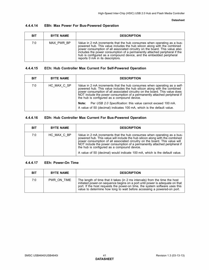
High-Speed Inter-Chip (HSIC) USB 2.0 Hub and Flash Media Controller
Datasheet
4.4.4.14 EBh: Max Power For Bus-Powered Operation
4.4.4.15 ECh: Hub Controller Max Current For Self-Powered Operation
4.4.4.16 EDh: Hub Controller Max Current For Bus-Powered Operation
4.4.4.17 EEh: Power-On Time
BIT BYTE NAME DESCRIPTION
7:0 MAX_PWR_BP Value in 2 mA increments that the hub consumes when operating as a bus-powered hub. This value includes the hub silicon along with the combined power consumption of all associated circuitry on the board. This value also includes the power consumption of a permanently attached peripheral if the hub is configured as a compound device, and the embedded peripheral reports 0 mA in its descriptors.
BIT BYTE NAME DESCRIPTION
7:0 HC_MAX_C_SP Value in 2 mA increments that the hub consumes when operating as a self-powered hub. This value includes the hub silicon along with the combined power consumption of all associated circuitry on the board. This value does NOT include the power consumption of a permanently attached peripheral if the hub is configured as a compound device.
Note: Per USB 2.0 Specification: this value cannot exceed 100 mA.
A value of 50 (decimal) indicates 100 mA, which is the default value.
BIT BYTE NAME DESCRIPTION
7:0 HC_MAX_C_BP Value in 2 mA increments that the hub consumes when operating as a bus-powered hub. This value will include the hub silicon along with the combined power consumption of all associated circuitry on the board. This value will NOT include the power consumption of a permanently attached peripheral if the hub is configured as a compound device.
A value of 50 (decimal) would indicate 100 mA, which is the default value.
BIT BYTE NAME DESCRIPTION
7:0 PWR_ON_TIME The length of time that it takes (in 2 ms intervals) from the time the host initiated power-on sequence begins on a port until power is adequate on that port. If the host requests the power-on time, the system software uses this value to determine how long to wait before accessing a powered-on port.
SMSC USB4640/USB4640i 41 Revision 1.3 (03-13-13)DATASHEET
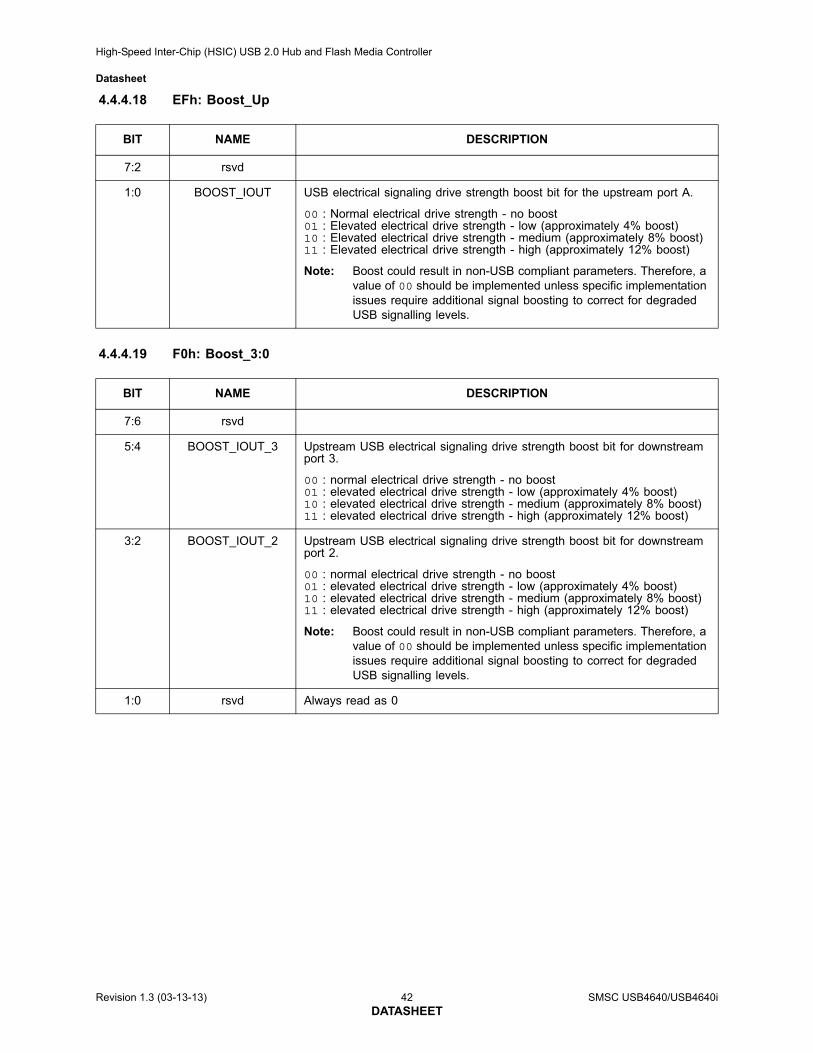
High-Speed Inter-Chip (HSIC) USB 2.0 Hub and Flash Media Controller
Datasheet
4.4.4.18 EFh: Boost_Up
4.4.4.19 F0h: Boost_3:0
BIT NAME DESCRIPTION
7:2 rsvd
1:0 BOOST_IOUT USB electrical signaling drive strength boost bit for the upstream port A.
00 : Normal electrical drive strength - no boost01 : Elevated electrical drive strength - low (approximately 4% boost)10 : Elevated electrical drive strength - medium (approximately 8% boost)11 : Elevated electrical drive strength - high (approximately 12% boost)
Note: Boost could result in non-USB compliant parameters. Therefore, a value of 00 should be implemented unless specific implementation issues require additional signal boosting to correct for degraded USB signalling levels.
BIT NAME DESCRIPTION
7:6 rsvd
5:4 BOOST_IOUT_3 Upstream USB electrical signaling drive strength boost bit for downstream port 3.
00 : normal electrical drive strength - no boost01 : elevated electrical drive strength - low (approximately 4% boost)10 : elevated electrical drive strength - medium (approximately 8% boost)11 : elevated electrical drive strength - high (approximately 12% boost)
3:2 BOOST_IOUT_2 Upstream USB electrical signaling drive strength boost bit for downstream port 2.
00 : normal electrical drive strength - no boost01 : elevated electrical drive strength - low (approximately 4% boost)10 : elevated electrical drive strength - medium (approximately 8% boost)11 : elevated electrical drive strength - high (approximately 12% boost)
Note: Boost could result in non-USB compliant parameters. Therefore, a value of 00 should be implemented unless specific implementation issues require additional signal boosting to correct for degraded USB signalling levels.
1:0 rsvd Always read as 0
Revision 1.3 (03-13-13) 42 SMSC USB4640/USB4640iDATASHEET
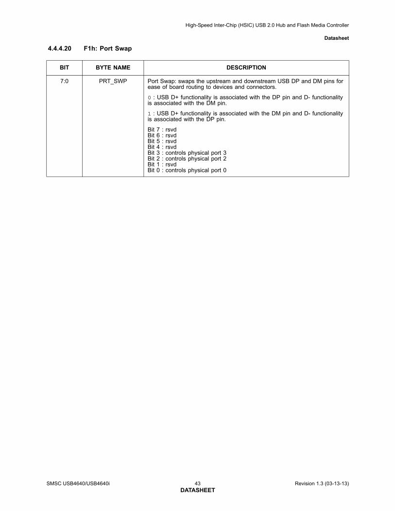
High-Speed Inter-Chip (HSIC) USB 2.0 Hub and Flash Media Controller
Datasheet
4.4.4.20 F1h: Port Swap
BIT BYTE NAME DESCRIPTION
7:0 PRT_SWP Port Swap: swaps the upstream and downstream USB DP and DM pins for ease of board routing to devices and connectors.
0 : USB D+ functionality is associated with the DP pin and D- functionality is associated with the DM pin.
1 : USB D+ functionality is associated with the DM pin and D- functionality is associated with the DP pin.
Bit 7 : rsvdBit 6 : rsvdBit 5 : rsvdBit 4 : rsvdBit 3 : controls physical port 3Bit 2 : controls physical port 2Bit 1 : rsvdBit 0 : controls physical port 0
SMSC USB4640/USB4640i 43 Revision 1.3 (03-13-13)DATASHEET
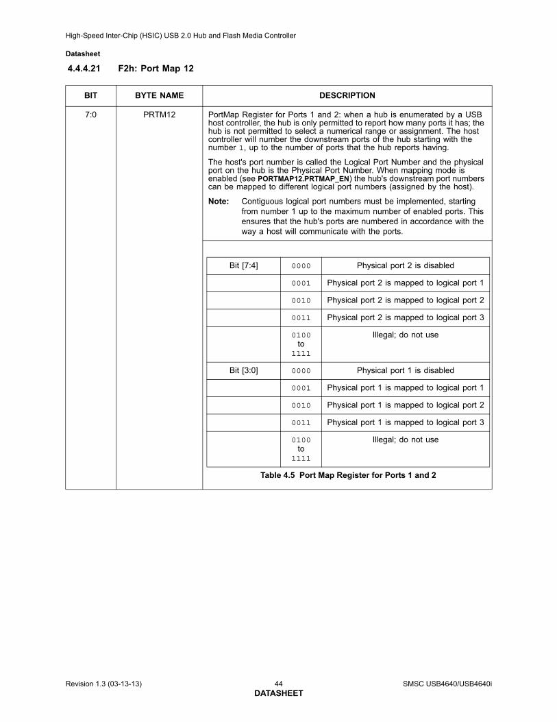
High-Speed Inter-Chip (HSIC) USB 2.0 Hub and Flash Media Controller
Datasheet
4.4.4.21 F2h: Port Map 12
BIT BYTE NAME DESCRIPTION
7:0 PRTM12 PortMap Register for Ports 1 and 2: when a hub is enumerated by a USB host controller, the hub is only permitted to report how many ports it has; the hub is not permitted to select a numerical range or assignment. The host controller will number the downstream ports of the hub starting with the number 1, up to the number of ports that the hub reports having.
The host's port number is called the Logical Port Number and the physical port on the hub is the Physical Port Number. When mapping mode is enabled (see PORTMAP12.PRTMAP_EN) the hub's downstream port numbers can be mapped to different logical port numbers (assigned by the host).
Note: Contiguous logical port numbers must be implemented, starting from number 1 up to the maximum number of enabled ports. This ensures that the hub's ports are numbered in accordance with the way a host will communicate with the ports.
Bit [7:4] 0000 Physical port 2 is disabled
0001 Physical port 2 is mapped to logical port 1
0010 Physical port 2 is mapped to logical port 2
0011 Physical port 2 is mapped to logical port 3
0100to
1111
Illegal; do not use
Bit [3:0] 0000 Physical port 1 is disabled
0001 Physical port 1 is mapped to logical port 1
0010 Physical port 1 is mapped to logical port 2
0011 Physical port 1 is mapped to logical port 3
0100to
1111
Illegal; do not use
Table 4.5 Port Map Register for Ports 1 and 2
Revision 1.3 (03-13-13) 44 SMSC USB4640/USB4640iDATASHEET
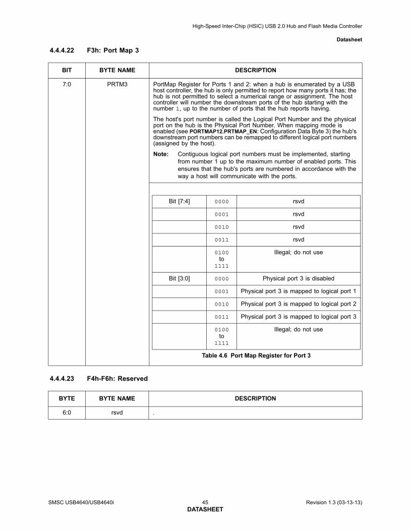
High-Speed Inter-Chip (HSIC) USB 2.0 Hub and Flash Media Controller
Datasheet
4.4.4.22 F3h: Port Map 3
4.4.4.23 F4h-F6h: Reserved
BIT BYTE NAME DESCRIPTION
7:0 PRTM3 PortMap Register for Ports 1 and 2: when a hub is enumerated by a USB host controller, the hub is only permitted to report how many ports it has; the hub is not permitted to select a numerical range or assignment. The host controller will number the downstream ports of the hub starting with the number 1, up to the number of ports that the hub reports having.
The host's port number is called the Logical Port Number and the physical port on the hub is the Physical Port Number. When mapping mode is enabled (see PORTMAP12.PRTMAP_EN: Configuration Data Byte 3) the hub's downstream port numbers can be remapped to different logical port numbers (assigned by the host).
Note: Contiguous logical port numbers must be implemented, starting from number 1 up to the maximum number of enabled ports. This ensures that the hub's ports are numbered in accordance with the way a host will communicate with the ports.
BYTE BYTE NAME DESCRIPTION
6:0 rsvd .
Bit [7:4] 0000 rsvd
0001 rsvd
0010 rsvd
0011 rsvd
0100to
1111
Illegal; do not use
Bit [3:0] 0000 Physical port 3 is disabled
0001 Physical port 3 is mapped to logical port 1
0010 Physical port 3 is mapped to logical port 2
0011 Physical port 3 is mapped to logical port 3
0100to
1111
Illegal; do not use
Table 4.6 Port Map Register for Port 3
SMSC USB4640/USB4640i 45 Revision 1.3 (03-13-13)DATASHEET
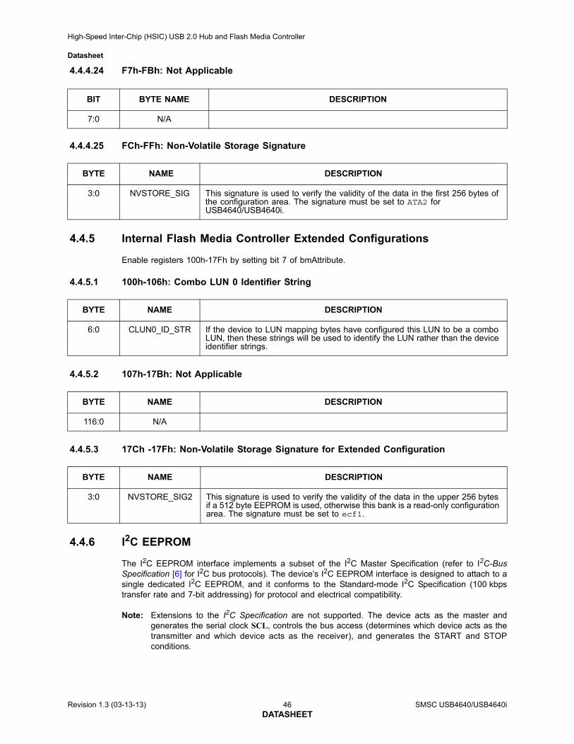
High-Speed Inter-Chip (HSIC) USB 2.0 Hub and Flash Media Controller
Datasheet
4.4.4.24 F7h-FBh: Not Applicable
4.4.4.25 FCh-FFh: Non-Volatile Storage Signature
4.4.5 Internal Flash Media Controller Extended Configurations
Enable registers 100h-17Fh by setting bit 7 of bmAttribute.
4.4.5.1 100h-106h: Combo LUN 0 Identifier String
4.4.5.2 107h-17Bh: Not Applicable
4.4.5.3 17Ch -17Fh: Non-Volatile Storage Signature for Extended Configuration
4.4.6 I2C EEPROM
The I2C EEPROM interface implements a subset of the I2C Master Specification (refer to I2C-BusSpecification [6] for I2C bus protocols). The device’s I2C EEPROM interface is designed to attach to asingle dedicated I2C EEPROM, and it conforms to the Standard-mode I2C Specification (100 kbpstransfer rate and 7-bit addressing) for protocol and electrical compatibility.
Note: Extensions to the I2C Specification are not supported. The device acts as the master andgenerates the serial clock SCL, controls the bus access (determines which device acts as thetransmitter and which device acts as the receiver), and generates the START and STOPconditions.
BIT BYTE NAME DESCRIPTION
7:0 N/A
BYTE NAME DESCRIPTION
3:0 NVSTORE_SIG This signature is used to verify the validity of the data in the first 256 bytes of the configuration area. The signature must be set to ATA2 for USB4640/USB4640i.
BYTE NAME DESCRIPTION
6:0 CLUN0_ID_STR If the device to LUN mapping bytes have configured this LUN to be a combo LUN, then these strings will be used to identify the LUN rather than the device identifier strings.
BYTE NAME DESCRIPTION
116:0 N/A
BYTE NAME DESCRIPTION
3:0 NVSTORE_SIG2 This signature is used to verify the validity of the data in the upper 256 bytes if a 512 byte EEPROM is used, otherwise this bank is a read-only configuration area. The signature must be set to ecf1.
Revision 1.3 (03-13-13) 46 SMSC USB4640/USB4640iDATASHEET
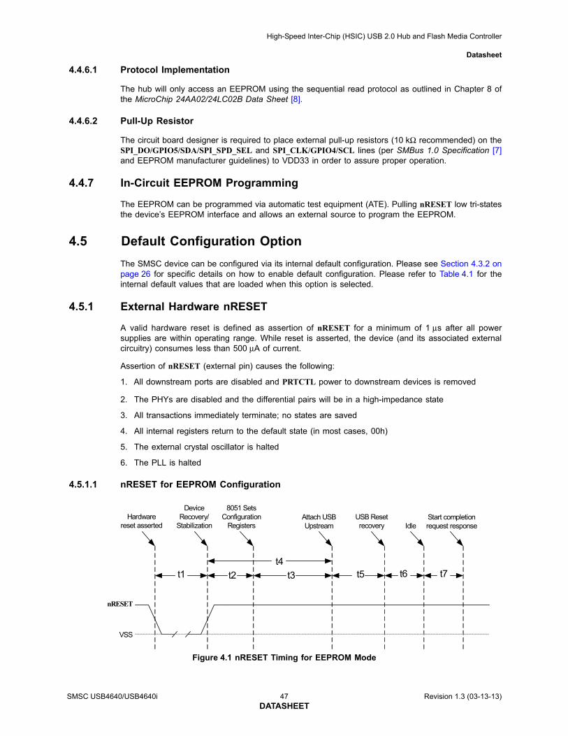
High-Speed Inter-Chip (HSIC) USB 2.0 Hub and Flash Media Controller
Datasheet
4.4.6.1 Protocol Implementation
The hub will only access an EEPROM using the sequential read protocol as outlined in Chapter 8 ofthe MicroChip 24AA02/24LC02B Data Sheet [8].
4.4.6.2 Pull-Up Resistor
The circuit board designer is required to place external pull-up resistors (10 kΩ recommended) on theSPI_DO/GPIO5/SDA/SPI_SPD_SEL and SPI_CLK/GPIO4/SCL lines (per SMBus 1.0 Specification [7]and EEPROM manufacturer guidelines) to VDD33 in order to assure proper operation.
4.4.7 In-Circuit EEPROM Programming
The EEPROM can be programmed via automatic test equipment (ATE). Pulling nRESET low tri-statesthe device’s EEPROM interface and allows an external source to program the EEPROM.
4.5 Default Configuration Option
The SMSC device can be configured via its internal default configuration. Please see Section 4.3.2 onpage 26 for specific details on how to enable default configuration. Please refer to Table 4.1 for theinternal default values that are loaded when this option is selected.
4.5.1 External Hardware nRESET
A valid hardware reset is defined as assertion of nRESET for a minimum of 1 μs after all powersupplies are within operating range. While reset is asserted, the device (and its associated externalcircuitry) consumes less than 500 μA of current.
Assertion of nRESET (external pin) causes the following:
1. All downstream ports are disabled and PRTCTL power to downstream devices is removed
2. The PHYs are disabled and the differential pairs will be in a high-impedance state
3. All transactions immediately terminate; no states are saved
4. All internal registers return to the default state (in most cases, 00h)
5. The external crystal oscillator is halted
6. The PLL is halted
4.5.1.1 nRESET for EEPROM Configuration
Figure 4.1 nRESET Timing for EEPROM Mode
t1 t2
t4t5 t6 t7
nRESET
VSS
Hardware reset asserted
Device Recovery/
Stabilization
8051 Sets Configuration
RegistersAttach USB Upstream
USB Reset recovery Idle
Start completion request response
t3
SMSC USB4640/USB4640i 47 Revision 1.3 (03-13-13)DATASHEET
High-Speed Inter-Chip (HSIC) USB 2.0 Hub and Flash Media Controller
Datasheet
Note: All power supplies must have reached the operating levels mandated in Chapter 6 on page 51,prior to (or coincident with) the assertion of nRESET.
4.5.2 USB Bus Reset
In response to the upstream port signaling a reset to the device, the device does the following:
1. Sets default address to 0
2. Sets configuration to: Unconfigured
3. Negates PRTCTL[3:2] to all downstream ports
4. Clears all TT buffers
5. Moves device from suspended to active (if suspended)
6. Complies with Section 11.10 of the USB 2.0 Specification for behavior after completion of the resetsequence
Note: The device does not propagate the upstream USB reset to downstream devices.
The host then configures the device and the device’s downstream port devices in accordance with theUSB 2.0 Specification.
Table 4.7 nRESET Timing for EEPROM Mode
NAME DESCRIPTION MIN TYP MAX UNITS
t1 nRESET asserted 1 μsec
t2 Device recovery/stabilization 500 μsec
t3 8051 programs device configuration 20 50 msec
t4 USB attach (Note) 100 msec
t5 Host acknowledges attach and signals USB reset 100 msec
t6 USB idle Undefined msec
t7 Completion time for requests (with or without data stage)
5 msec
Revision 1.3 (03-13-13) 48 SMSC USB4640/USB4640iDATASHEET
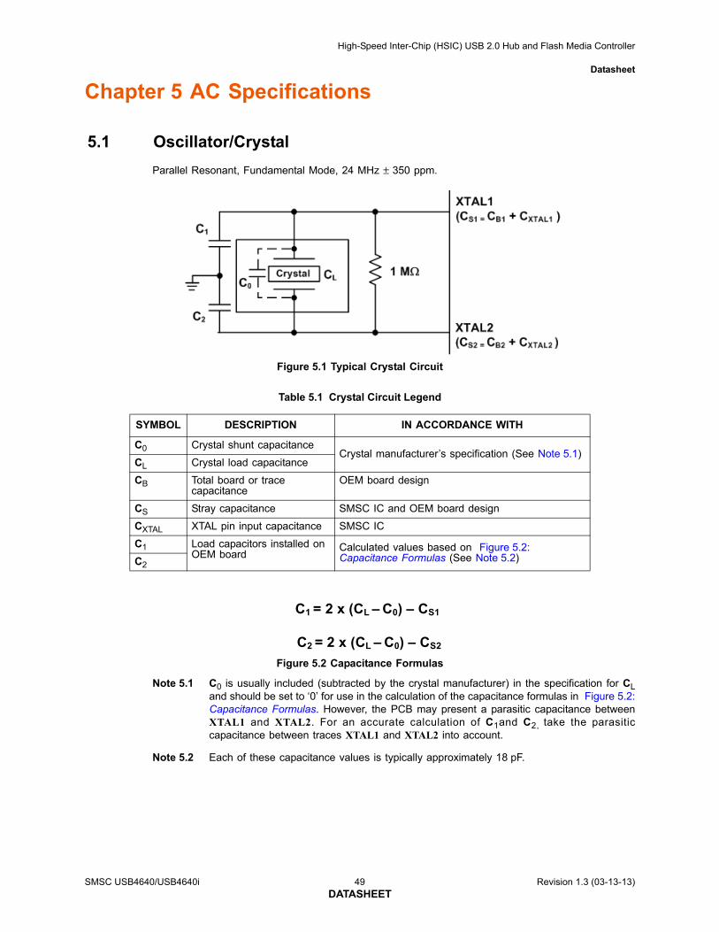
High-Speed Inter-Chip (HSIC) USB 2.0 Hub and Flash Media Controller
Datasheet
Chapter 5 AC Specifications
5.1 Oscillator/Crystal
Parallel Resonant, Fundamental Mode, 24 MHz ± 350 ppm.
Figure 5.1 Typical Crystal Circuit
Figure 5.2 Capacitance Formulas
Note 5.1 C0 is usually included (subtracted by the crystal manufacturer) in the specification for CLand should be set to ‘0’ for use in the calculation of the capacitance formulas in Figure 5.2:Capacitance Formulas. However, the PCB may present a parasitic capacitance betweenXTAL1 and XTAL2. For an accurate calculation of C1and C2, take the parasiticcapacitance between traces XTAL1 and XTAL2 into account.
Note 5.2 Each of these capacitance values is typically approximately 18 pF.
Table 5.1 Crystal Circuit Legend
SYMBOL DESCRIPTION IN ACCORDANCE WITH
C0 Crystal shunt capacitanceCrystal manufacturer’s specification (See Note 5.1)
CL Crystal load capacitance
CB Total board or trace capacitance
OEM board design
CS Stray capacitance SMSC IC and OEM board design
CXTAL XTAL pin input capacitance SMSC IC
C1 Load capacitors installed on OEM board
Calculated values based on Figure 5.2: Capacitance Formulas (See Note 5.2)C2
C1 = 2 x (CL – C0) – CS1
C2 = 2 x (CL – C0) – CS2
SMSC USB4640/USB4640i 49 Revision 1.3 (03-13-13)DATASHEET
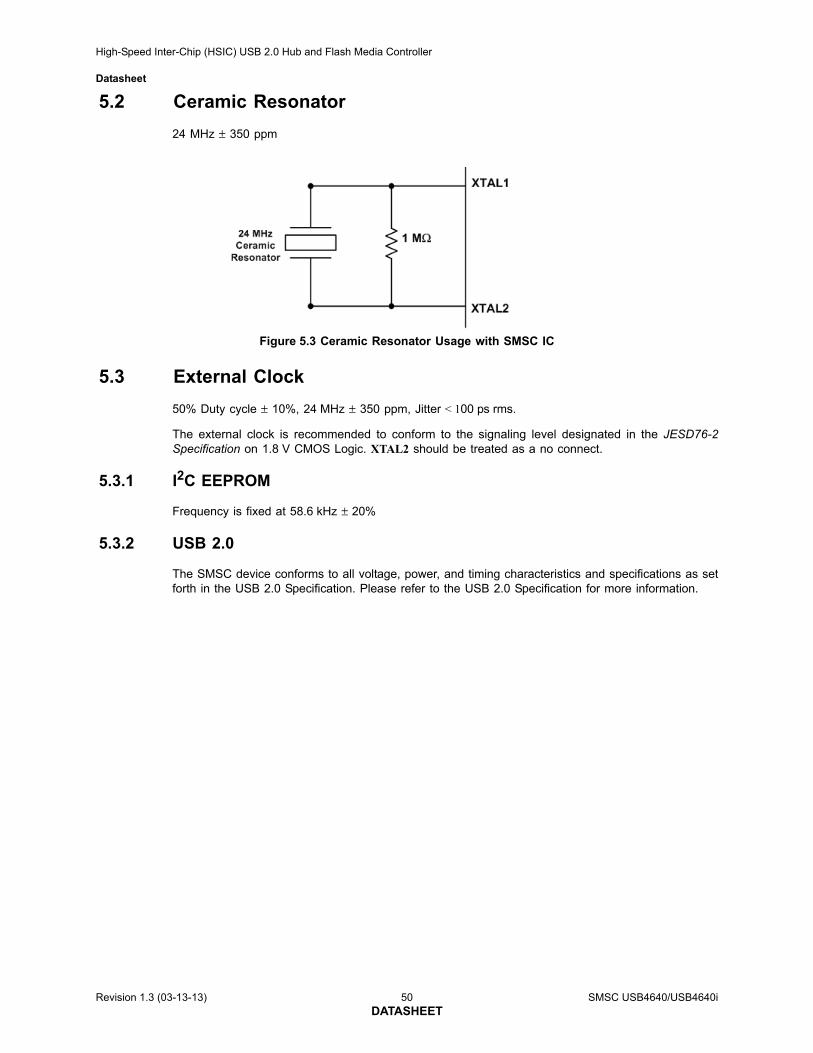
High-Speed Inter-Chip (HSIC) USB 2.0 Hub and Flash Media Controller
Datasheet
5.2 Ceramic Resonator
24 MHz ± 350 ppm
Figure 5.3 Ceramic Resonator Usage with SMSC IC
5.3 External Clock
50% Duty cycle ± 10%, 24 MHz ± 350 ppm, Jitter < 100 ps rms.
The external clock is recommended to conform to the signaling level designated in the JESD76-2Specification on 1.8 V CMOS Logic. XTAL2 should be treated as a no connect.
5.3.1 I2C EEPROM
Frequency is fixed at 58.6 kHz ± 20%
5.3.2 USB 2.0
The SMSC device conforms to all voltage, power, and timing characteristics and specifications as setforth in the USB 2.0 Specification. Please refer to the USB 2.0 Specification for more information.
Revision 1.3 (03-13-13) 50 SMSC USB4640/USB4640iDATASHEET
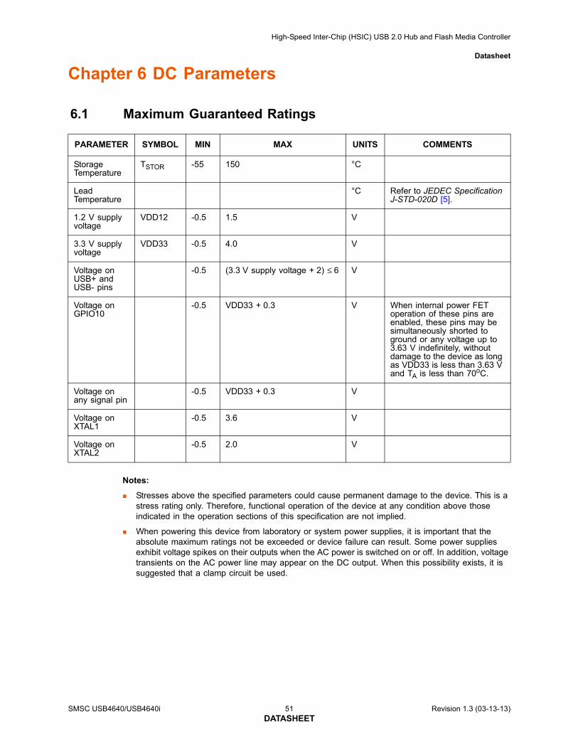
High-Speed Inter-Chip (HSIC) USB 2.0 Hub and Flash Media Controller
Datasheet
Chapter 6 DC Parameters
6.1 Maximum Guaranteed Ratings
Notes:
Stresses above the specified parameters could cause permanent damage to the device. This is a stress rating only. Therefore, functional operation of the device at any condition above those indicated in the operation sections of this specification are not implied.
When powering this device from laboratory or system power supplies, it is important that the absolute maximum ratings not be exceeded or device failure can result. Some power supplies exhibit voltage spikes on their outputs when the AC power is switched on or off. In addition, voltage transients on the AC power line may appear on the DC output. When this possibility exists, it is suggested that a clamp circuit be used.
PARAMETER SYMBOL MIN MAX UNITS COMMENTS
Storage Temperature
TSTOR -55 150 °C
Lead Temperature
°C Refer to JEDEC Specification J-STD-020D [5].
1.2 V supply voltage
VDD12 -0.5 1.5 V
3.3 V supply voltage
VDD33 -0.5 4.0 V
Voltage on USB+ and USB- pins
-0.5 (3.3 V supply voltage + 2) ≤ 6 V
Voltage on GPIO10
-0.5 VDD33 + 0.3 V When internal power FET operation of these pins are enabled, these pins may be simultaneously shorted to ground or any voltage up to 3.63 V indefinitely, without damage to the device as long as VDD33 is less than 3.63 V and TA is less than 70oC.
Voltage on any signal pin
-0.5 VDD33 + 0.3 V
Voltage on XTAL1
-0.5 3.6 V
Voltage on XTAL2
-0.5 2.0 V
SMSC USB4640/USB4640i 51 Revision 1.3 (03-13-13)DATASHEET
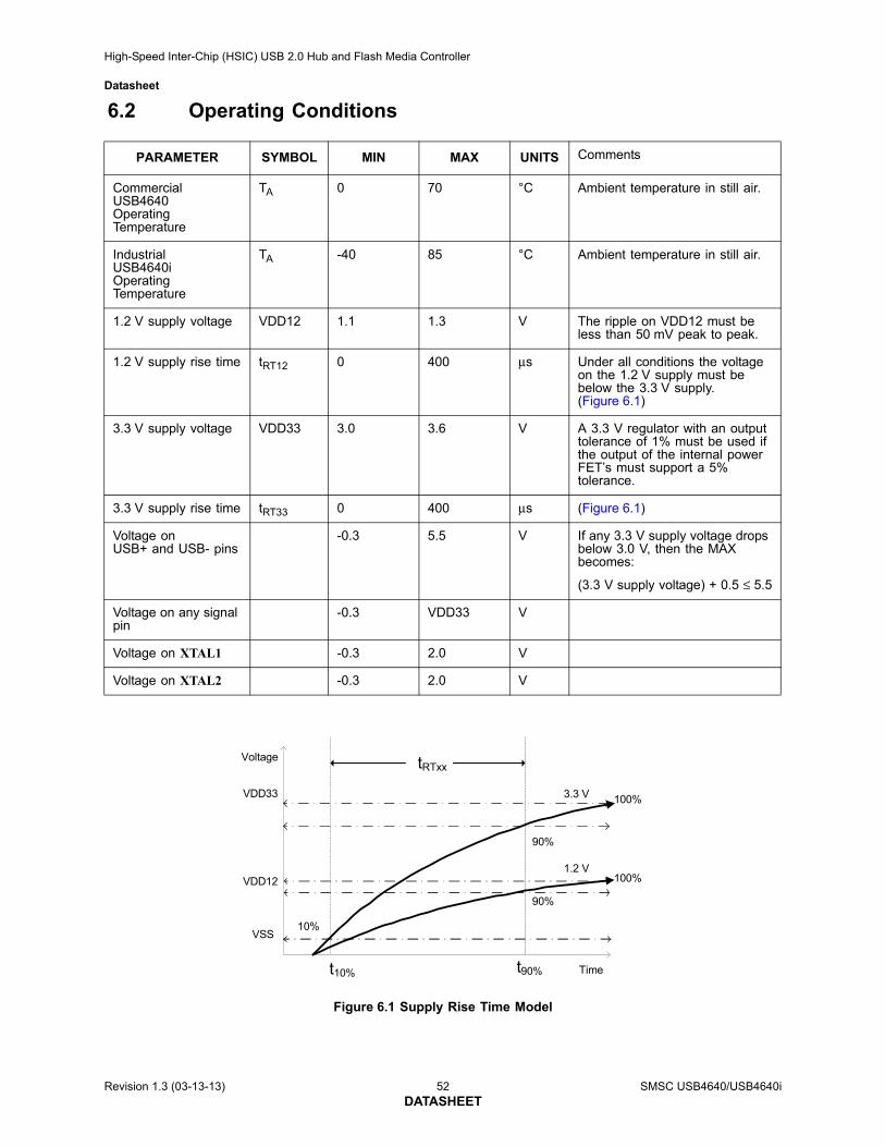
High-Speed Inter-Chip (HSIC) USB 2.0 Hub and Flash Media Controller
Datasheet
6.2 Operating Conditions
Figure 6.1 Supply Rise Time Model
PARAMETER SYMBOL MIN MAX UNITS Comments
CommercialUSB4640Operating Temperature
TA 0 70 °C Ambient temperature in still air.
IndustrialUSB4640iOperating Temperature
TA -40 85 °C Ambient temperature in still air.
1.2 V supply voltage VDD12 1.1 1.3 V The ripple on VDD12 must be less than 50 mV peak to peak.
1.2 V supply rise time tRT12 0 400 μs Under all conditions the voltage on the 1.2 V supply must be below the 3.3 V supply. (Figure 6.1)
3.3 V supply voltage VDD33 3.0 3.6 V A 3.3 V regulator with an output tolerance of 1% must be used if the output of the internal power FET’s must support a 5% tolerance.
3.3 V supply rise time tRT33 0 400 μs (Figure 6.1)
Voltage on USB+ and USB- pins
-0.3 5.5 V If any 3.3 V supply voltage drops below 3.0 V, then the MAX becomes:
(3.3 V supply voltage) + 0.5 ≤ 5.5
Voltage on any signal pin
-0.3 VDD33 V
Voltage on XTAL1 -0.3 2.0 V
Voltage on XTAL2 -0.3 2.0 V
t10%
10%
90%
Voltage tRTxx
t90% Time
100%3.3 V
VSS
VDD33
90%
100%1.2 V
VDD12
Revision 1.3 (03-13-13) 52 SMSC USB4640/USB4640iDATASHEET
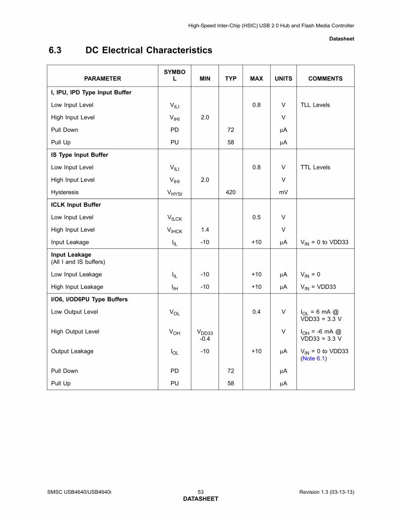
High-Speed Inter-Chip (HSIC) USB 2.0 Hub and Flash Media Controller
Datasheet
6.3 DC Electrical Characteristics
PARAMETERSYMBO
L MIN TYP MAX UNITS COMMENTS
I, IPU, IPD Type Input Buffer
Low Input Level VILI 0.8 V TLL Levels
High Input Level VIHI 2.0 V
Pull Down PD 72 μA
Pull Up PU 58 μA
IS Type Input Buffer
Low Input Level VILI 0.8 V TTL Levels
High Input Level VIHI 2.0 V
Hysteresis VHYSI 420 mV
ICLK Input Buffer
Low Input Level VILCK 0.5 V
High Input Level VIHCK 1.4 V
Input Leakage IIL -10 +10 μA VIN = 0 to VDD33
Input Leakage(All I and IS buffers)
Low Input Leakage IIL -10 +10 μA VIN = 0
High Input Leakage IIH -10 +10 μA VIN = VDD33
I/O6, I/OD6PU Type Buffers
Low Output Level VOL 0.4 V IOL = 6 mA @ VDD33 = 3.3 V
High Output Level VOH VDD33-0.4
V IOH = -6 mA @ VDD33 = 3.3 V
Output Leakage IOL -10 +10 μA VIN = 0 to VDD33(Note 6.1)
Pull Down PD 72 μA
Pull Up PU 58 μA
SMSC USB4640/USB4640i 53 Revision 1.3 (03-13-13)DATASHEET
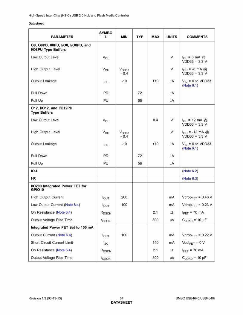
High-Speed Inter-Chip (HSIC) USB 2.0 Hub and Flash Media Controller
Datasheet
O8, O8PD, 08PU, I/O8, I/O8PD, and I/O8PU Type Buffers
Low Output Level VOL V IOL = 8 mA @ VDD33 = 3.3 V
High Output Level VOH VDD33 - 0.4
V IOH = -8 mA @ VDD33 = 3.3 V
Output Leakage IOL -10 +10 μA VIN = 0 to VDD33(Note 6.1)
Pull Down PD 72 μA
Pull Up PU 58 μA
O12, I/O12, and I/O12PDType Buffers
Low Output Level VOL 0.4 V IOL = 12 mA @ VDD33 = 3.3 V
High Output Level VOH VDD33 - 0.4
V IOH = -12 mA @ VDD33 = 3.3 V
Output Leakage IOL -10 +10 μA VIN = 0 to VDD33(Note 6.1)
Pull Down PD 72 μA
Pull Up PU 58 μA
IO-U (Note 6.2)
I-R (Note 6.3)
I/O200 Integrated Power FET for GPIO10
High Output Current IOUT 200 mA VdropFET = 0.46 V
Low Output Current (Note 6.4) IOUT 100 mA VdropFET = 0.23 V
On Resistance (Note 6.4) RDSON 2.1 Ω IFET = 70 mA
Output Voltage Rise Time tDSON 800 μs CLOAD = 10 μF
Integrated Power FET Set to 100 mA
Output Current (Note 6.4) IOUT 100 mA VdropFET = 0.22 V
Short Circuit Current Limit ISC 140 mA VoutFET = 0 V
On Resistance (Note 6.4) RDSON 2.1 Ω IFET = 70 mA
Output Voltage Rise Time tDSON 800 μs CLOAD = 10 μF
PARAMETERSYMBO
L MIN TYP MAX UNITS COMMENTS
Revision 1.3 (03-13-13) 54 SMSC USB4640/USB4640iDATASHEET
High-Speed Inter-Chip (HSIC) USB 2.0 Hub and Flash Media Controller
Datasheet
Note 6.1 Output leakage is measured with the current pins in high impedance.
Note 6.2 See the USB 2.0 Specification, Chapter 7, for USB DC electrical characteristics
Note 6.3 RBIAS is a 3.3 V tolerant analog pin.
Note 6.4 Output current range is controlled by program software. The software disables the FETduring short circuit condition.
Note 6.5 Refer to the High-Speed Inter-Chip USB Electrical Specification Revision 1.0 [2].
Note 6.6 Typical and maximum values were characterized using the following temperature ranges:The USB4640 supports the commercial temperature range of 0°C to +70°CThe USB4640i supports the industrial temperature range of -40°C to +85°C
Integrated Power FET Set to 200 mA
Output Current (Note 6.4) IOUT 200 mA VdropFET = 0.46 V
Short Circuit Current Limit ISC 181 mA VoutFET = 0 V
On Resistance (Note 6.4) RDSON 2.1 Ω IFET = 70 mA
Output Voltage Rise Time tDSON 800 μs CLOAD = 10 μF
Supply Current Unconfigured (Note 6.6)
USB4640 ICCINTHS 58 60 mA
USB4640i ICCINTHS 58 62 mA
Supply Current Configured1 downstream port
(Note 6.6)
USB4640 IHCH1 155 160 mA
USB4640i IHCH1 155 165 mA
Supply Current ConfiguredEach additional downstream port
(Note 6.6)
USB4640 30 35 mA
USB4640i 30 40 mA
HSIC_DAT, HSIC_STROBEDriver Impedance
ID 40 46 60 Ω (Note 6.5)
Supply Current Suspend (Note 6.6)
USB4640 ICSBY 210 375 µA
USB4640i ICSBY 210 450 µA
Supply Current Reset (Note 6.6)
USB4640 IRST 220 400 µA
USB4640i IRST 220 500 µA
PARAMETERSYMBO
L MIN TYP MAX UNITS COMMENTS
SMSC USB4640/USB4640i 55 Revision 1.3 (03-13-13)DATASHEET
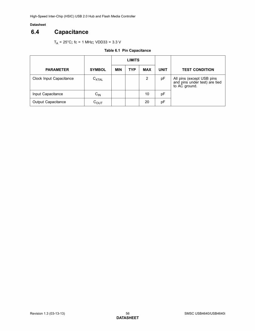
High-Speed Inter-Chip (HSIC) USB 2.0 Hub and Flash Media Controller
Datasheet
6.4 Capacitance
TA = 25°C; fc = 1 MHz; VDD33 = 3.3 V
Table 6.1 Pin Capacitance
PARAMETER SYMBOL
LIMITS
UNIT TEST CONDITIONMIN TYP MAX
Clock Input Capacitance CXTAL 2 pF All pins (except USB pins and pins under test) are tied to AC ground.
Input Capacitance CIN 10 pF
Output Capacitance COUT 20 pF
Revision 1.3 (03-13-13) 56 SMSC USB4640/USB4640iDATASHEET
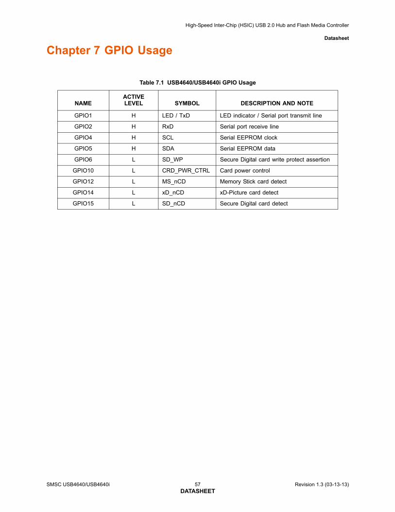
High-Speed Inter-Chip (HSIC) USB 2.0 Hub and Flash Media Controller
Datasheet
SMSC USB4640/USB4640i 57 Revision 1.3 (03-13-13)DATASHEET
Chapter 7 GPIO Usage
Table 7.1 USB4640/USB4640i GPIO Usage
NAMEACTIVE LEVEL SYMBOL DESCRIPTION AND NOTE
GPIO1 H LED / TxD LED indicator / Serial port transmit line
GPIO2 H RxD Serial port receive line
GPIO4 H SCL Serial EEPROM clock
GPIO5 H SDA Serial EEPROM data
GPIO6 L SD_WP Secure Digital card write protect assertion
GPIO10 L CRD_PWR_CTRL Card power control
GPIO12 L MS_nCD Memory Stick card detect
GPIO14 L xD_nCD xD-Picture card detect
GPIO15 L SD_nCD Secure Digital card detect
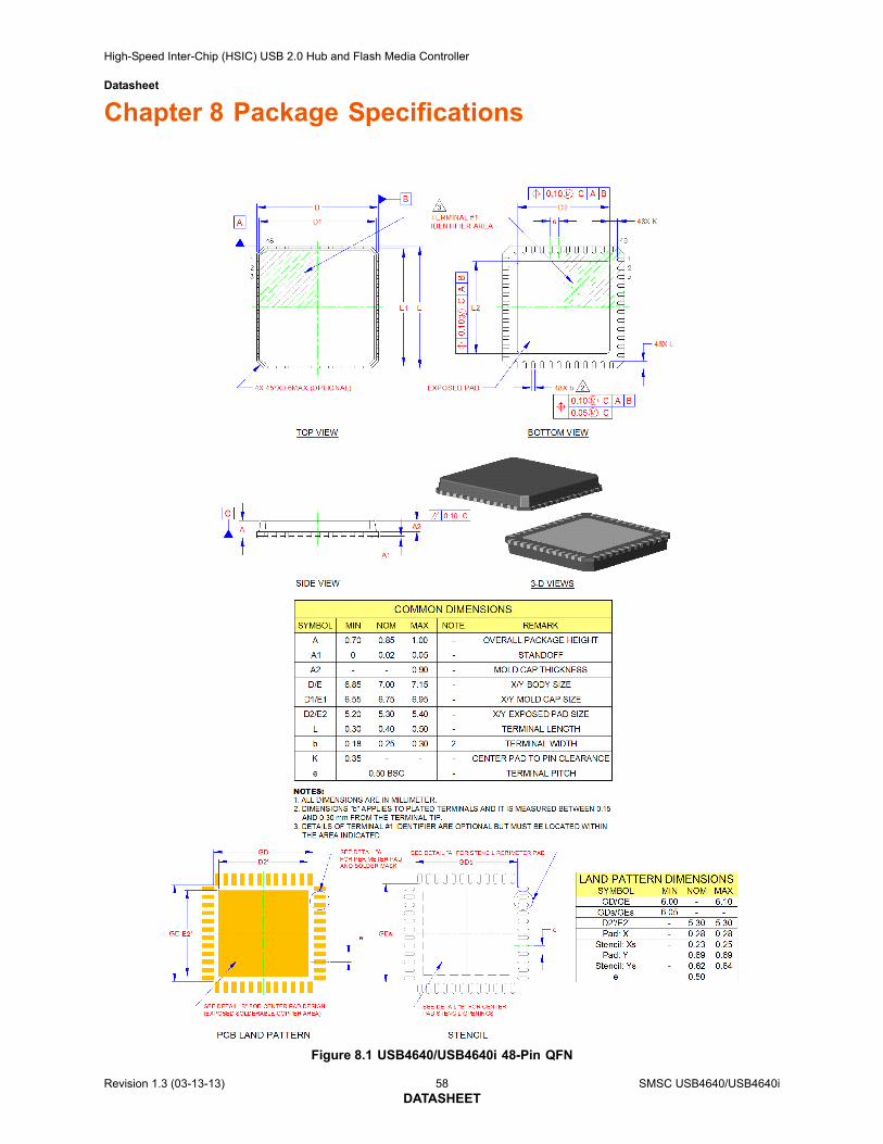
High-Speed Inter-Chip (HSIC) USB 2.0 Hub and Flash Media Controller
Datasheet
Chapter 8 Package Specifications
Figure 8.1 USB4640/USB4640i 48-Pin QFN
Revision 1.3 (03-13-13) 58 SMSC USB4640/USB4640iDATASHEET
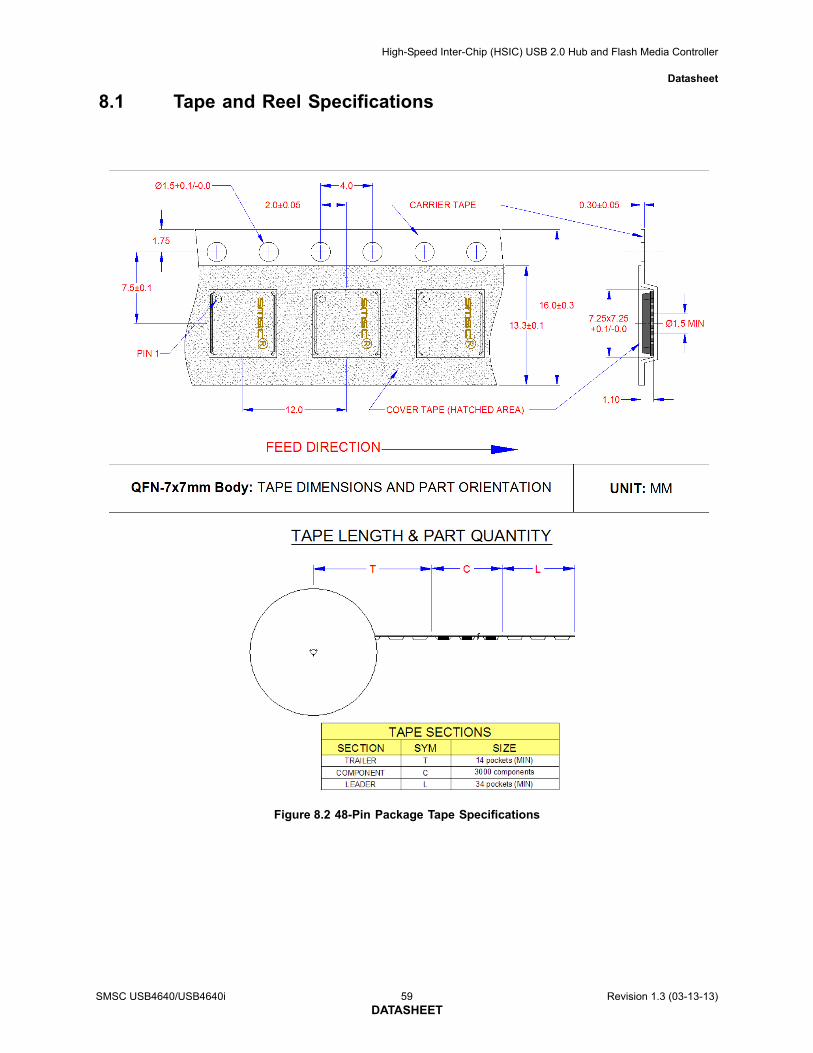
High-Speed Inter-Chip (HSIC) USB 2.0 Hub and Flash Media Controller
Datasheet
8.1 Tape and Reel Specifications
Figure 8.2 48-Pin Package Tape Specifications
SMSC USB4640/USB4640i 59 Revision 1.3 (03-13-13)DATASHEET
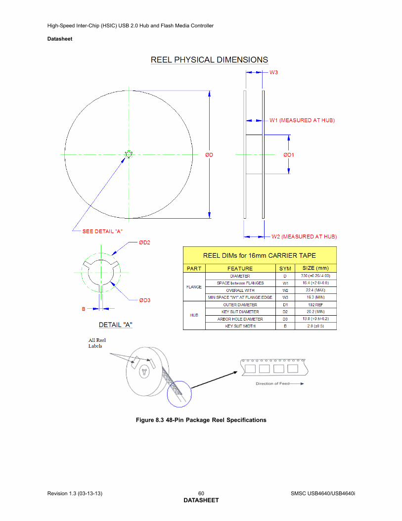
High-Speed Inter-Chip (HSIC) USB 2.0 Hub and Flash Media Controller
Datasheet
Figure 8.3 48-Pin Package Reel Specifications
Revision 1.3 (03-13-13) 60 SMSC USB4640/USB4640iDATASHEET
High-Speed Inter-Chip (HSIC) USB 2.0 Hub and Flash Media Controller
Datasheet
SMSC USB4640/USB4640i 61 Revision 1.3 (03-13-13)DATASHEET
Appendix A (Acronyms)
ACK: Handshake packet (positive acknowledgement)
EOF: End of (micro) Frame
FM: Flash Media
FMC: Flash Media Controller
FS: Full-Speed Device
LS: Low-Speed Device
HS: Hi-Speed Device
I2C®: Inter-Integrated Circuit1
MMC: MultiMediaCard
MS: Memory Stick
MSC: Memory Stick Controller
OCS: Over-current Sense
PHY: Physical Layer
PLL: Phase-Locked Loop
SD: Secure Digital
SDC: Secure Digital Controller
TXD: Transmit eXchange Data
UART: Universal Asynchronous Receiver-Transmitter
UCHAR: Unsigned Character
UINT: Unsigned Integer
Standard Microsystems is a registered trademark and SMSC is a trademark of Standard Microsystems Corporation. Other product and company namesare trademarks or registered trademarks of their respective holders.
*Note: In order to develop, make, use, or sell readers and/or other products using or incorporating any of the SMSC devices made the subject of thisdocument or to use related SMSC software programs, technical information and licenses under patent and other intellectual property rights from or throughvarious persons or entities, including without limitation media standard companies, forums, and associations, and other patent holders may be required.These media standard companies, forums, and associations include without limitation the following: Sony Corporation (Memory Stick, Memory Stick Pro);SD3 LLC (Secure Digital); MultiMedia Card Association (MultiMediaCard); the SSFDC Forum (SmartMedia); the Compact Flash Association (CompactFlash); and Fuji Photo Film Co., Ltd., Olympus Optical Co., Ltd., and Toshiba Corporation (xD-Picture Card). SMSC does not make such licenses ortechnical information available; does not promise or represent that any such licenses or technical information will actually be obtainable from or throughthe various persons or entities (including the media standard companies, forums, and associations), or with respect to the terms under which they maybe made available; and is not responsible for the accuracy or sufficiency of, or otherwise with respect to, any such technical information.
SMSC's obligations (if any) under the Terms of Sale Agreement, or any other agreement with any customer, or otherwise, with respect to infringement,including without limitation any obligations to defend or settle claims, to reimburse for costs, or to pay damages, shall not apply to any of the devicesmade the subject of this document or any software programs related to any of such devices, or to any combinations involving any of them, with respectto infringement or claimed infringement of any existing or future patents related to solid state disk or other flash memory technology or applications (“SolidState Disk Patents”). By making any purchase of any of the devices made the subject of this document, the customer represents, warrants, and agreesthat it has obtained all necessary licenses under then-existing Solid State Disk Patents for the manufacture, use and sale of solid state disk and otherflash memory products and that the customer will timely obtain at no cost or expense to SMSC all necessary licenses under Solid State Disk Patents;that the manufacture and testing by or for SMSC of the units of any of the devices made the subject of this document which may be sold to the customer,and any sale by SMSC of such units to the customer, are valid exercises of the customer's rights and licenses under such Solid State Disk Patents; thatSMSC shall have no obligation for royalties or otherwise under any Solid State Disk Patents by reason of any such manufacture, use, or sale of suchunits; and that SMSC shall have no obligation for any costs or expenses related to the customer's obtaining or having obtained rights or licenses underany Solid State Disk Patents. SMSC MAKES NO WARRANTIES, EXPRESS, IMPLIED, OR STATUTORY, IN REGARD TO INFRINGEMENT OR OTHERVIOLATION OF INTELLECTUAL PROPERTY RIGHTS. SMSC DISCLAIMS AND EXCLUDES ANY AND ALL WARRANTIES AGAINSTINFRINGEMENT AND THE LIKE.
No license is granted by SMSC expressly, by implication, by estoppel or otherwise, under any patent, trademark, copyright, mask work right, trade secret,or other intellectual property right.
**To obtain this software program the appropriate SMSC Software License Agreement must be executed and in effect. Forms of these Software LicenseAgreements may be obtained by contacting SMSC.
1. I2C is a registered trademark of Philips Corporation.
High-Speed Inter-Chip (HSIC) USB 2.0 Hub and Flash Media Controller
Datasheet
Revision 1.3 (03-13-13) 62 SMSC USB4640/USB4640iDATASHEET
Appendix B (References)
[1] Universal Serial Bus Specification, Version 2.0, April 27, 2000 (12/7/2000 and 5/28/2002 Errata)
USB Implementers Forum, Inc. http://www.usb.org
[2] USB 2.0 Supplement High-Speed Inter-Chip USB Electrical Specification Revision 1.0. 09/23/07.
USB Implementers Forum, Inc. http://www.usb.org/developers/docs/
[3] HSIC ECN. May 25, 2010
USB Implementers Forum, Inc. http://www.usb.org/developers/docs/
[4] The Unicode Standard, Worldwide Character Encoding Version 4.0
The Unicode Consortium. http://www.unicode.org
[5] JEDEC Specification J-STD-020D
JEDEC Global Standards for the Microelectronics Industry.http://www.jedec.org/standards-documents
[6] I2C-Bus Specification Version 1.1
NXP (formerly a division of Philips). http://www.nxp.com/products/interface_control/i2c/
[7] System Management Bus Specification, version 1.0
SMBus. http://smbus.org/specs/
[8] MicroChip 24AA02/24LC02B
Microchip Technology Inc. http://www.microchip.com/