Embed Size (px)
Citation preview
Use of FTDI devices in life support and/or safety applications is entirely at the user’s risk, and the
user agrees to defend, indemnify and hold FTDI harmless from any and all damages, claims, suits or expense resulting from such use.
Future Technology Devices International Limited (FTDI)
Unit 1, 2 Seaward Place, Glasgow G41 1HH, United Kingdom Tel.: +44 (0) 141 429 2777 Fax: + 44 (0) 141 429 2758
Web Site: http://ftdichip.com Copyright © Future Technology Devices International Limited
Application Note
AN_394
User Guide for FT260
Version 1.0
Issue Date: 2016-03-08
The FT260 is a USB device which supports I²C and UART communication through the standard USB HID interface. This guide describes the FT260 HID
report formats, and is intended for developers who are creating applications,
extending FTDI provided applications or implementing FTDI’s applications for the FT260.
Application Note
AN_394 User Guide for FT260 V ers ion 1 .0
Document Reference No.: FT_001279 C learance No.: FTDI# 488
2 P roduc t Page
Document Feedback C opyright © Future Technology Devices International Limited
Table of Contents
1 Introduction ............................................................ 5
1.1 Overview.......................................................................... 5
1.2 FT260 HID Interfaces and Endpoints ................................. 6
1.2.1 Interfaces ...................................................................................... 6
1.2.2 Endpoints....................................................................................... 6
1.3 Scope ............................................................................... 7
2 Wiring ..................................................................... 8
2.1 I²C ................................................................................... 8
2.2 UART................................................................................ 8
3 Getting Started ...................................................... 10
4 FT260 HID Reports ................................................ 13
4.1 HID Class Requests for Reports....................................... 13
4.1.1 Get Report .................................................................................... 13
4.1.2 Set Report .................................................................................... 14
4.2 HID Report Structure ...................................................... 14
4.3 FT260 Report ID List....................................................... 15
4.4 System Status Reports.................................................... 16
4.4.1 Chip Version .................................................................................. 16
4.4.2 Get System Status.......................................................................... 16
4.4.3 Set System Clock ........................................................................... 18
4.4.4 Set UART Mode .............................................................................. 18
4.4.5 Enable Interrupt/Wake up ................................................................ 19
4.4.6 Select GPIO2 Function ..................................................................... 19
4.4.7 Enable UART DCD RI ....................................................................... 19
4.4.8 Select GPIOA Function..................................................................... 20
4.4.9 Select GPIOG Function .................................................................... 20
4.4.10 Set Interrupt Trigger Condition ......................................................... 21
4.4.11 Set Suspend Out Polarity ................................................................. 21
Application Note
AN_394 User Guide for FT260 V ers ion 1 .0
Document Reference No.: FT_001279 C learance No.: FTDI# 488
3 P roduc t Page
Document Feedback C opyright © Future Technology Devices International Limited
4.4.12 Enable UART RI Wakeup .................................................................. 21
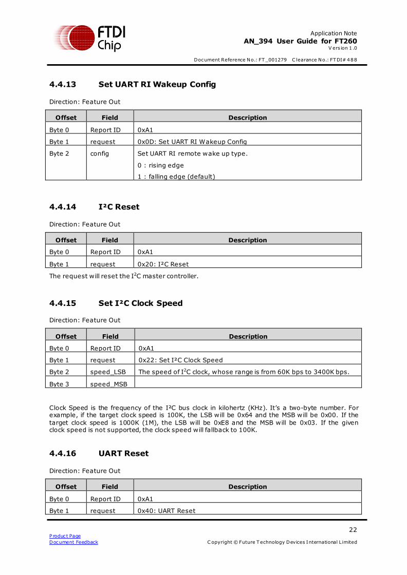
4.4.13 Set UART RI Wakeup Config ............................................................. 22
4.4.14 I²C Reset ...................................................................................... 22
4.4.15 Set I²C Clock Speed........................................................................ 22
4.4.16 UART Reset ................................................................................... 22
4.4.17 Configure UART .............................................................................. 23
4.4.18 Set UART Baud Rate ....................................................................... 25
4.4.19 Set UART Data Bit .......................................................................... 25
4.4.20 Set UART Parity ............................................................................. 25
4.4.21 Set UART Stop Bit .......................................................................... 26
4.4.22 Set UART Breaking ......................................................................... 26
4.4.23 Set UART XON / XOFF ..................................................................... 26
4.5 I²C ................................................................................. 27
4.5.1 Get I²C Status ............................................................................... 28
4.5.2 I²C Write Request........................................................................... 29
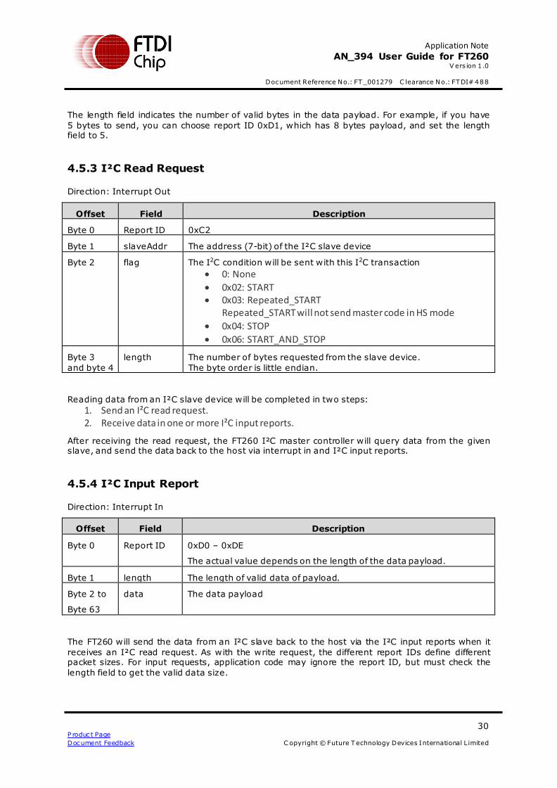
4.5.3 I²C Read Request ........................................................................... 30
4.5.4 I²C Input Report ............................................................................ 30
4.6 UART.............................................................................. 31
4.6.1 Get UART Settings .......................................................................... 31
4.6.2 UART Write Request ........................................................................ 32
4.6.3 UART Input Report.......................................................................... 32
4.6.4 Get DCD & RI Status ....................................................................... 33
4.7 GPIO .............................................................................. 33
4.7.1 GPIO Write Request ........................................................................ 33
4.7.2 GPIO Read Request ........................................................................ 33
4.8 Interrupt Report ............................................................. 34
5 Sample Code to perform search with libudev .......... 35
6 Contact Information .............................................. 41
Appendix A – References ........................................... 42
Document References ............................................................ 42

Application Note
AN_394 User Guide for FT260 V ers ion 1 .0
Document Reference No.: FT_001279 C learance No.: FTDI# 488
4 P roduc t Page
Document Feedback C opyright © Future Technology Devices International Limited
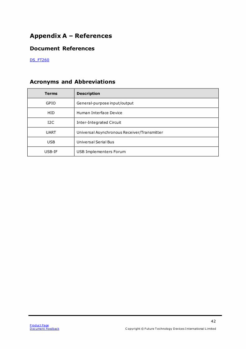
Acronyms and Abbreviations .................................................. 42
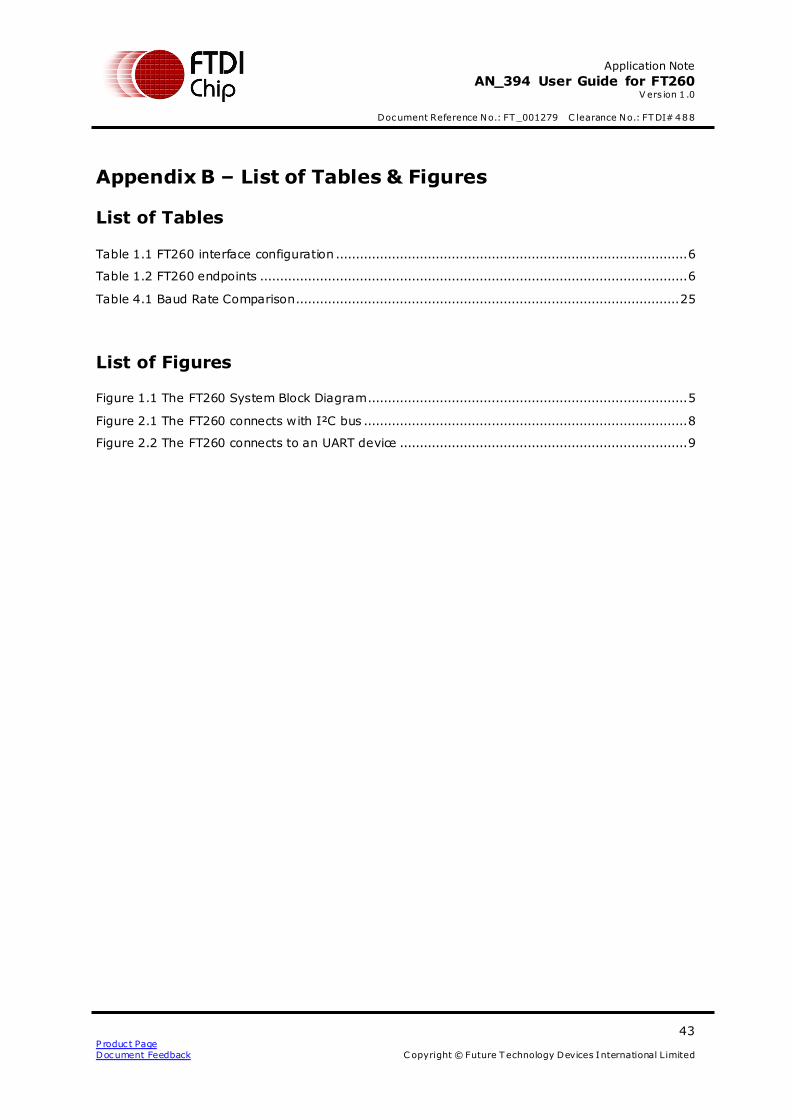
Appendix B – List of Tables & Figures ......................... 43
List of Tables ......................................................................... 43
List of Figures ........................................................................ 43
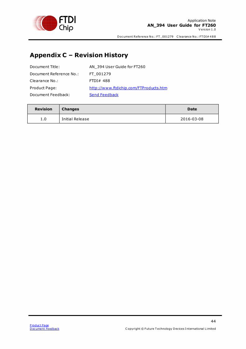
Appendix C – Revision History .................................... 44
Application Note
AN_394 User Guide for FT260 V ers ion 1 .0
Document Reference No.: FT_001279 C learance No.: FTDI# 488
5 P roduc t Page
Document Feedback C opyright © Future Technology Devices International Limited
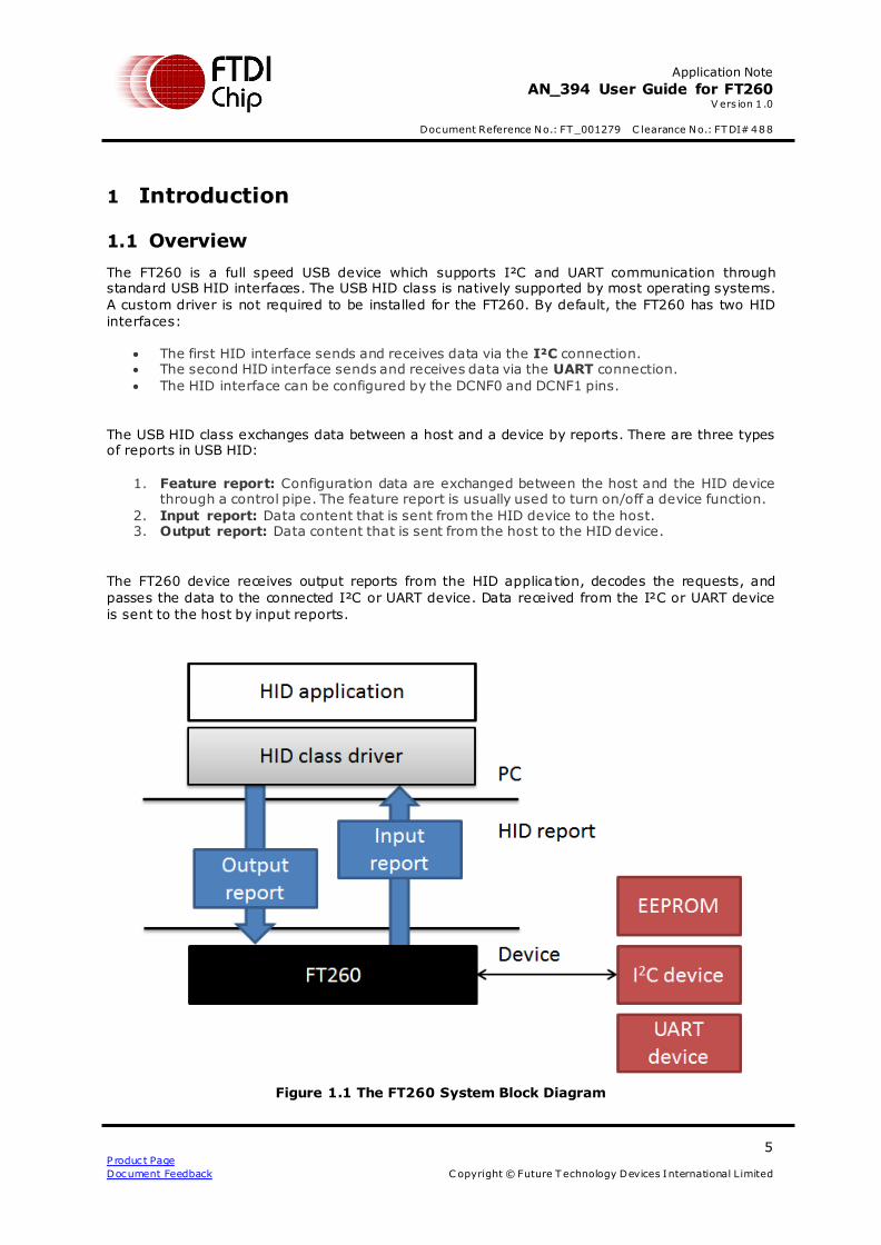
1 Introduction
1.1 Overview
The FT260 is a full speed USB device which supports I²C and UART communication through standard USB HID interfaces. The USB HID class is natively supported by most operating systems.
A custom driver is not required to be installed for the FT260. By default, the FT260 has two HID
interfaces:
The first HID interface sends and receives data via the I²C connection. The second HID interface sends and receives data via the UART connection.
The HID interface can be configured by the DCNF0 and DCNF1 pins.
The USB HID class exchanges data between a host and a device by reports. There are three types of reports in USB HID:
1. Feature report: Configuration data are exchanged between the host and the HID device through a control pipe. The feature report is usually used to turn on/off a device function.
2. Input report: Data content that is sent from the HID device to the host. 3. Output report: Data content that is sent from the host to the HID device.
The FT260 device receives output reports from the HID application, decodes the requests, and
passes the data to the connected I²C or UART device. Data received from the I²C or UART device
is sent to the host by input reports.
Figure 1.1 The FT260 System Block Diagram
Application Note
AN_394 User Guide for FT260 V ers ion 1 .0
Document Reference No.: FT_001279 C learance No.: FTDI# 488
6 P roduc t Page
Document Feedback C opyright © Future Technology Devices International Limited
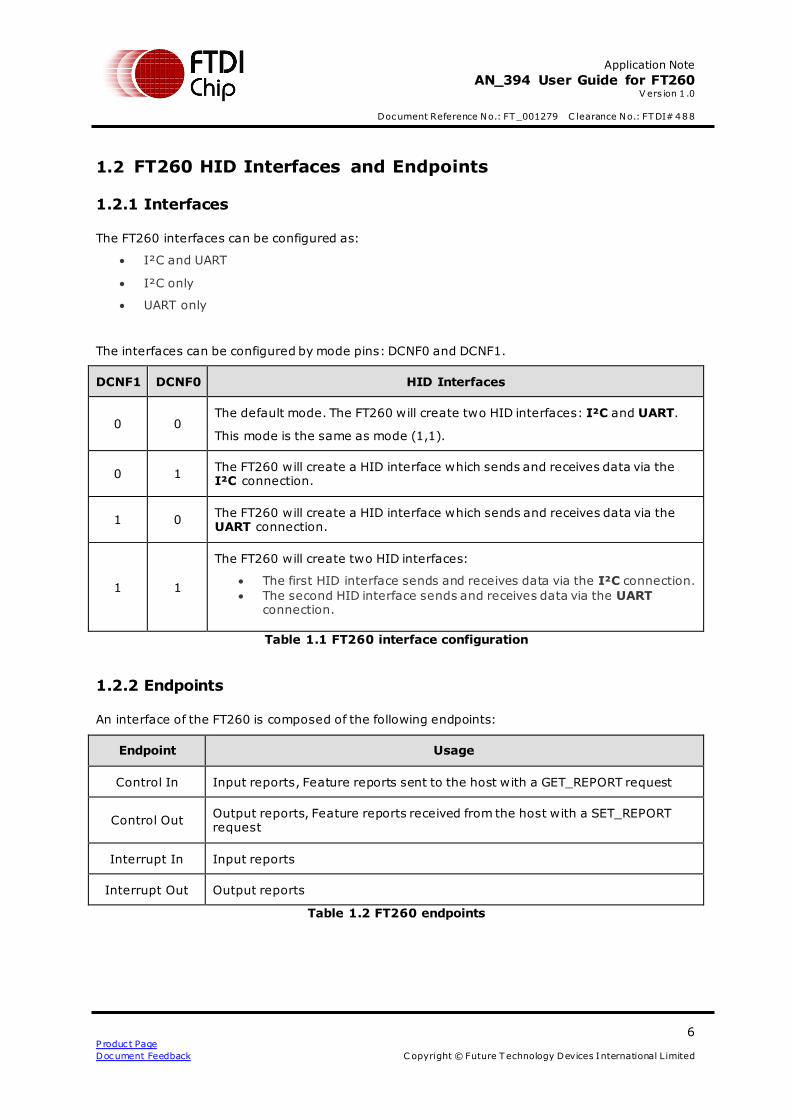
1.2 FT260 HID Interfaces and Endpoints
1.2.1 Interfaces
The FT260 interfaces can be configured as:
I²C and UART
I²C only
UART only
The interfaces can be configured by mode pins: DCNF0 and DCNF1.
DCNF1 DCNF0 HID Interfaces
0 0 The default mode. The FT260 will create two HID interfaces: I²C and UART.
This mode is the same as mode (1,1).
0 1 The FT260 will create a HID interface which sends and receives data via the I²C connection.
1 0 The FT260 will create a HID interface which sends and receives data via the UART connection.
1 1
The FT260 will create two HID interfaces:
The first HID interface sends and receives data via the I²C connection.
The second HID interface sends and receives data via the UART connection.
Table 1.1 FT260 interface configuration
1.2.2 Endpoints
An interface of the FT260 is composed of the following endpoints:
Endpoint Usage
Control In Input reports, Feature reports sent to the host with a GET_REPORT request
Control Out Output reports, Feature reports received from the host with a SET_REPORT request
Interrupt In Input reports
Interrupt Out Output reports
Table 1.2 FT260 endpoints
Application Note
AN_394 User Guide for FT260 V ers ion 1 .0
Document Reference No.: FT_001279 C learance No.: FTDI# 488
7 P roduc t Page
Document Feedback C opyright © Future Technology Devices International Limited
1.3 Scope
This guide describes the FT260 HID report formats, and is intended for developers who are
creating applications, extending FTDI provided applications or implementing FTDI’s applications for
the FT260.
The sample source code contained in this application note is provided as an example and is neither guaranteed nor supported by FTDI.
Application Note
AN_394 User Guide for FT260 V ers ion 1 .0
Document Reference No.: FT_001279 C learance No.: FTDI# 488
8 P roduc t Page
Document Feedback C opyright © Future Technology Devices International Limited
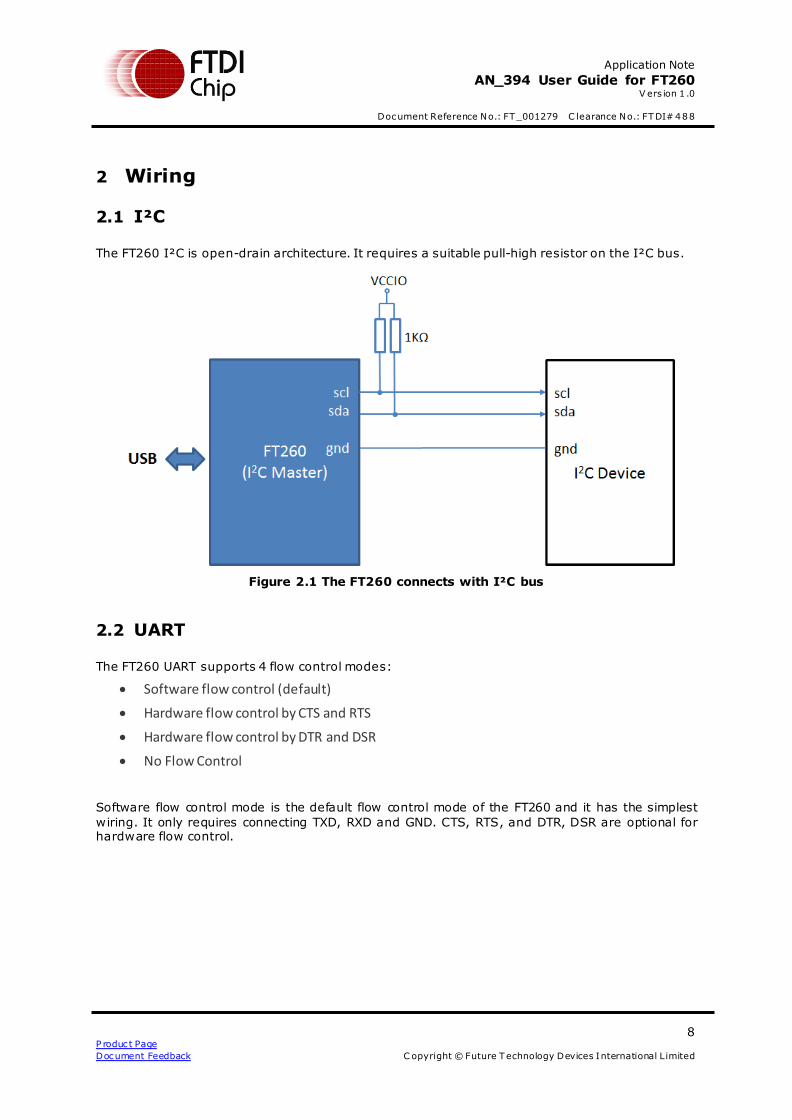
2 Wiring
2.1 I²C
The FT260 I²C is open-drain architecture. It requires a suitable pull-high resistor on the I²C bus.
Figure 2.1 The FT260 connects with I²C bus
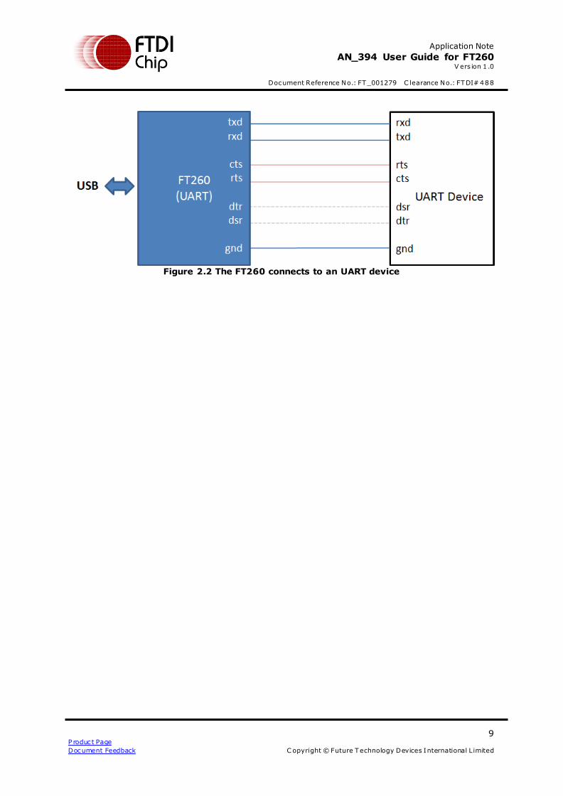
2.2 UART
The FT260 UART supports 4 flow control modes:
Software flow control (default)
Hardware flow control by CTS and RTS
Hardware flow control by DTR and DSR
No Flow Control
Software flow control mode is the default flow control mode of the FT260 and it has the simplest
wiring. It only requires connecting TXD, RXD and GND. CTS, RTS, and DTR, DSR are optional for hardware flow control.
Application Note
AN_394 User Guide for FT260 V ers ion 1 .0
Document Reference No.: FT_001279 C learance No.: FTDI# 488
9 P roduc t Page
Document Feedback C opyright © Future Technology Devices International Limited
Figure 2.2 The FT260 connects to an UART device
Application Note
AN_394 User Guide for FT260 V ers ion 1 .0
Document Reference No.: FT_001279 C learance No.: FTDI# 488
10 P roduc t Page
Document Feedback C opyright © Future Technology Devices International Limited
3 Getting Started
This is a simple example which shows how to work with the FT260 on a Linux platform.
Open the HID device by device path
Get the info about the device driver using an ioctl function, which communicates with the underlying device driver to get parameters.
Send requests to the FT260
Example
#include <linux/types.h> #include <linux/input.h> #include <linux/hidraw.h> /* * For the systems that don't have the new version of hidraw.h in userspace. */ #ifndef HIDIOCSFEATURE #warning Please have your distro update the userspace kernel headers #define HIDIOCSFEATURE(len) _IOC(_IOC_WRITE|_IOC_READ, 'H', 0x06, len) #define HIDIOCGFEATURE(len) _IOC(_IOC_WRITE|_IOC_READ, 'H', 0x07, len) #endif #include <sys/ioctl.h> #include <sys/types.h> #include <sys/stat.h> #include <fcntl.h> #include <unistd.h> #include <stdio.h> #include <string.h> #include <stdlib.h> #include <errno.h> const char* bus_type_str(int bus) { switch (bus) { case BUS_USB: return "USB"; case BUS_HIL: return "HIL"; case BUS_BLUETOOTH: return "Bluetooth"; case BUS_VIRTUAL: return "Virtual"; default: return "Other"; } } int main(int argc, char **argv) { int fd; int res, desc_size = 0; char buf[256]; struct hidraw_report_descriptor rpt_desc; struct hidraw_devinfo info; char* device = "/dev/hidraw0"; if (argc > 1) { device = argv[1]; }
Application Note
AN_394 User Guide for FT260 V ers ion 1 .0
Document Reference No.: FT_001279 C learance No.: FTDI# 488
11 P roduc t Page
Document Feedback C opyright © Future Technology Devices International Limited
/* Open the Device with non-blocking reads. */ /* It will be better if use libudev instead of hard coded path. You can check Appendix A for the example of using libudev */ fd = open(device, O_RDWR|O_NONBLOCK); if (fd < 0) { perror("Unable to open device"); return 1; } memset(&rpt_desc, 0x0, sizeof(rpt_desc)); memset(&info, 0x0, sizeof(info)); memset(buf, 0x0, sizeof(buf)); /* Get Report Descriptor Size */ res = ioctl(fd, HIDIOCGRDESCSIZE, &desc_size); if (res < 0) { perror("HIDIOCGRDESCSIZE"); } else { printf("Report Descriptor Size: %d\n", desc_size); } /* Get Raw Name */
res = ioctl(fd, HIDIOCGRAWNAME(256), buf); if (res < 0) { perror("HIDIOCGRAWNAME"); } else { printf("Raw Name: %s\n", buf); } /* Get Raw Info */ res = ioctl(fd, HIDIOCGRAWINFO, &info); if (res < 0) { perror("HIDIOCGRAWINFO"); } else { printf("Raw Info:\n"); printf("\tbustype: %d (%s)\n", info.bustype, bus_type_str(info.bustype)); printf("\tvendor: 0x%04hx\n", info.vendor); printf("\tproduct: 0x%04hx\n", info.product); } /* Set Feature */ buf[0] = 0xA1; /* SYSTEM_SETTING_ID */ buf[1] = 0x22; /* I2C_SPEED */ buf[2] = 0x01; /* 400Kbps */ buf[3] = 0x90; res = ioctl(fd, HIDIOCSFEATURE(4), buf); if (res < 0) { perror("HIDIOCSFEATURE"); } else { printf("ioctl HIDIOCGFEATURE returned: %d\n", res); } /* Send a Report to the Device */ buf[0] = 0xD0; /* I2C write */ buf[1] = 0x22; /* Slave address */ buf[2] = 0x06; /* Start and Stop */ buf[3] = 0x03; /* data len */
Application Note
AN_394 User Guide for FT260 V ers ion 1 .0
Document Reference No.: FT_001279 C learance No.: FTDI# 488
12 P roduc t Page
Document Feedback C opyright © Future Technology Devices International Limited
buf[4] = 'a'; buf[5] = 'b'; buf[6] = 'c'; res = write(fd, buf, 7); if (res < 0) { printf("Error: %d\n", errno); perror("write"); } else { printf("write() wrote %d bytes\n", res); } close(fd); return 0; }
Application Note
AN_394 User Guide for FT260 V ers ion 1 .0
Document Reference No.: FT_001279 C learance No.: FTDI# 488
13 P roduc t Page
Document Feedback C opyright © Future Technology Devices International Limited
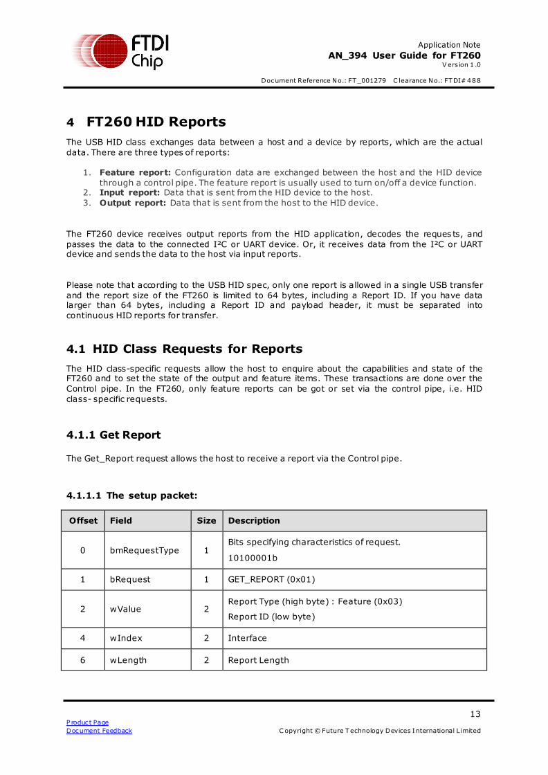
4 FT260 HID Reports
The USB HID class exchanges data between a host and a device by reports, which are the actual
data. There are three types of reports:
1. Feature report: Configuration data are exchanged between the host and the HID device
through a control pipe. The feature report is usually used to turn on/off a device function. 2. Input report: Data that is sent from the HID device to the host.
3. Output report: Data that is sent from the host to the HID device.
The FT260 device receives output reports from the HID application, decodes the reques ts, and
passes the data to the connected I²C or UART device. Or, it receives data from the I²C or UART device and sends the data to the host via input reports.
Please note that according to the USB HID spec, only one report is allowed in a single USB transfer
and the report size of the FT260 is limited to 64 bytes, including a Report ID. If you have data larger than 64 bytes, including a Report ID and payload header, it must be separated into
continuous HID reports for transfer.
4.1 HID Class Requests for Reports
The HID class-specific requests allow the host to enquire about the capabilities and state of the FT260 and to set the state of the output and feature items. These transactions are done over the
Control pipe. In the FT260, only feature reports can be got or set via the control pipe, i.e. HID
class- specific requests.
4.1.1 Get Report
The Get_Report request allows the host to receive a report via the Control pipe.
4.1.1.1 The setup packet:
Offset Field Size Description
0 bmRequestType 1 Bits specifying characteristics of request.
10100001b
1 bRequest 1 GET_REPORT (0x01)
2 wValue 2 Report Type (high byte) : Feature (0x03)
Report ID (low byte)
4 wIndex 2 Interface
6 wLength 2 Report Length
Application Note
AN_394 User Guide for FT260 V ers ion 1 .0
Document Reference No.: FT_001279 C learance No.: FTDI# 488
14 P roduc t Page
Document Feedback C opyright © Future Technology Devices International Limited
4.1.1.2 The Data stage:
The HID report will be received in the data stage.
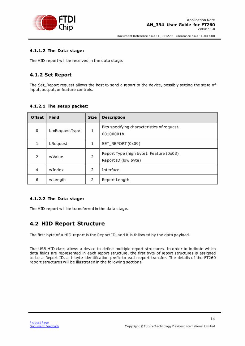
4.1.2 Set Report
The Set_Report request allows the host to send a report to the device, possibly setting the state of
input, output, or feature controls.
4.1.2.1 The setup packet:
Offset Field Size Description
0 bmRequestType 1 Bits specifying characteristics of request.
00100001b
1 bRequest 1 SET_REPORT (0x09)
2 wValue 2 Report Type (high byte): Feature (0x03)
Report ID (low byte)
4 wIndex 2 Interface
6 wLength 2 Report Length
4.1.2.2 The Data stage:
The HID report will be transferred in the data stage.
4.2 HID Report Structure
The first byte of a HID report is the Report ID, and it is followed by the data payload.
The USB HID class allows a device to define multiple report structures. In order to indicate which data fields are represented in each report structure, the first byte of report structures is assigned
to be a Report ID, a 1-byte identification prefix to each report transfer. The details of the FT260 report structures will be illustrated in the following sections.
Application Note
AN_394 User Guide for FT260 V ers ion 1 .0
Document Reference No.: FT_001279 C learance No.: FTDI# 488
15 P roduc t Page
Document Feedback C opyright © Future Technology Devices International Limited
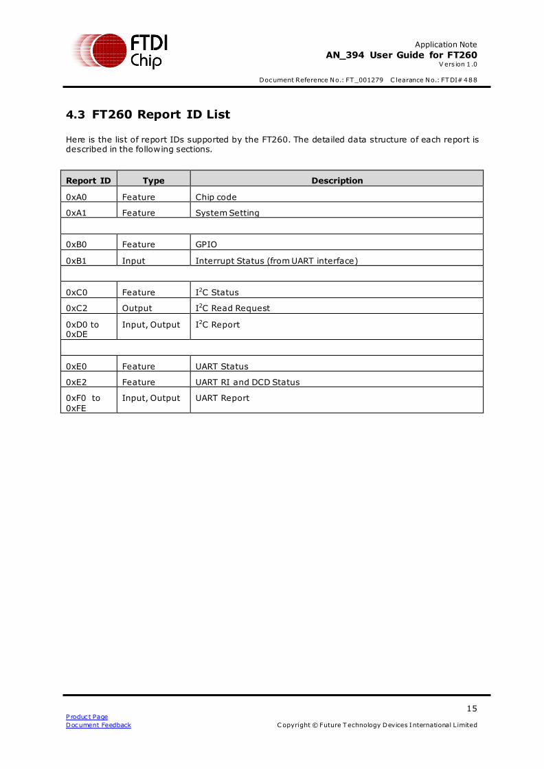
4.3 FT260 Report ID List
Here is the list of report IDs supported by the FT260. The detailed data structure of each report is described in the following sections.
Report ID Type Description
0xA0 Feature Chip code
0xA1 Feature System Setting
0xB0 Feature GPIO
0xB1 Input Interrupt Status (from UART interface)
0xC0 Feature I2C Status
0xC2 Output I2C Read Request
0xD0 to 0xDE
Input, Output I2C Report
0xE0 Feature UART Status
0xE2 Feature UART RI and DCD Status
0xF0 to
0xFE
Input, Output UART Report
Application Note
AN_394 User Guide for FT260 V ers ion 1 .0
Document Reference No.: FT_001279 C learance No.: FTDI# 488
16 P roduc t Page
Document Feedback C opyright © Future Technology Devices International Limited
4.4 System Status Reports
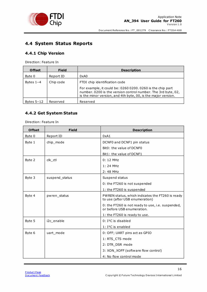
4.4.1 Chip Version
Direction: Feature In
Offset Field Description
Byte 0 Report ID 0xA0
Bytes 1–4 Chip code FTDI chip identification code
For example, it could be: 0260 0200. 0260 is the chip part
number. 0200 is the version control number. The 3rd byte, 02, is the minor version, and 4th byte, 00, is the major version.
Bytes 5–12 Reserved Reserved
4.4.2 Get System Status
Direction: Feature In
Offset Field Description
Byte 0 Report ID 0xA1
Byte 1 chip_mode DCNF0 and DCNF1 pin status
Bit0: the value of DCNF0
Bit1: the value of DCNF1
Byte 2 clk_ctl 0: 12 MHz
1: 24 MHz
2: 48 MHz
Byte 3 suspend_status Suspend status
0: the FT260 is not suspended
1: the FT260 is suspended
Byte 4 pwren_status PWREN status, which indicates the FT260 is ready to use (after USB enumeration)
0: the FT260 is not ready to use, i.e. suspended,
or before USB enumeration.
1: the FT260 is ready to use.
Byte 5 i2c_enable 0: I²C is disabled
1: I²C is enabled
Byte 6 uart_mode 0: OFF; UART pins act as GPIO
1: RTS_CTS mode
2: DTR_DSR mode
3: XON_XOFF (software flow control)
4: No flow control mode
Application Note
AN_394 User Guide for FT260 V ers ion 1 .0
Document Reference No.: FT_001279 C learance No.: FTDI# 488
17 P roduc t Page
Document Feedback C opyright © Future Technology Devices International Limited
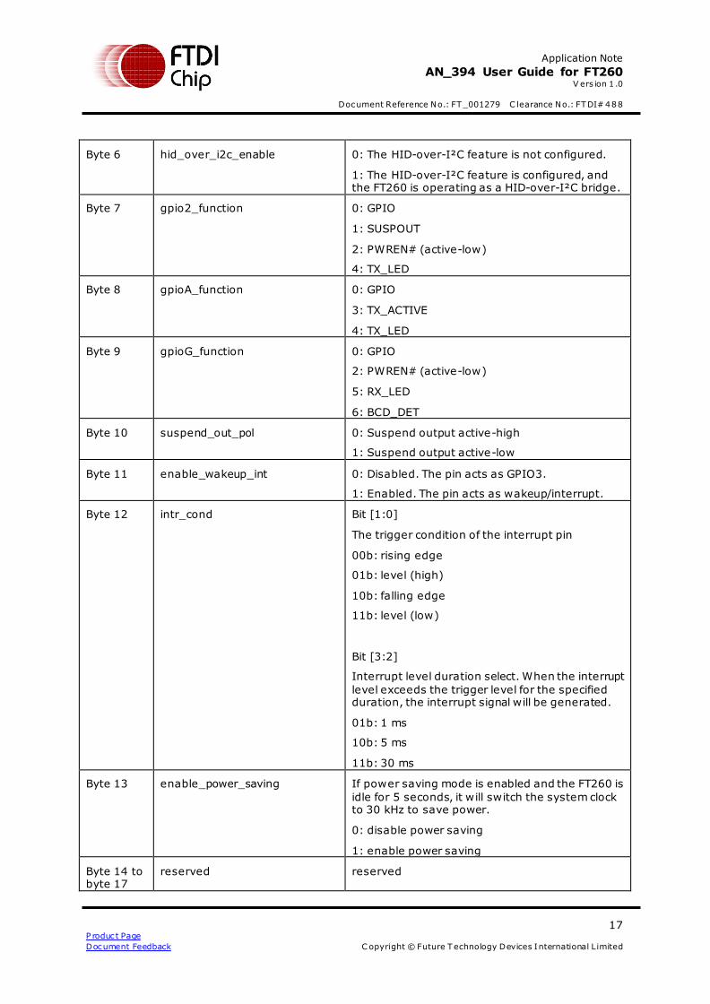
Byte 6 hid_over_i2c_enable 0: The HID-over-I²C feature is not configured.
1: The HID-over-I²C feature is configured, and the FT260 is operating as a HID-over-I²C bridge.
Byte 7 gpio2_function 0: GPIO
1: SUSPOUT
2: PWREN# (active-low)
4: TX_LED
Byte 8 gpioA_function 0: GPIO
3: TX_ACTIVE
4: TX_LED
Byte 9 gpioG_function 0: GPIO
2: PWREN# (active-low)
5: RX_LED
6: BCD_DET
Byte 10 suspend_out_pol 0: Suspend output active-high
1: Suspend output active-low
Byte 11 enable_wakeup_int 0: Disabled. The pin acts as GPIO3.
1: Enabled. The pin acts as wakeup/interrupt.
Byte 12 intr_cond Bit [1:0]
The trigger condition of the interrupt pin
00b: rising edge
01b: level (high)
10b: falling edge
11b: level (low)
Bit [3:2]
Interrupt level duration select. When the interrupt
level exceeds the trigger level for the specified duration, the interrupt signal will be generated.
01b: 1 ms
10b: 5 ms
11b: 30 ms
Byte 13 enable_power_saving If power saving mode is enabled and the FT260 is
idle for 5 seconds, it will switch the system clock to 30 kHz to save power.
0: disable power saving
1: enable power saving
Byte 14 to byte 17
reserved reserved
Application Note
AN_394 User Guide for FT260 V ers ion 1 .0
Document Reference No.: FT_001279 C learance No.: FTDI# 488
18 P roduc t Page
Document Feedback C opyright © Future Technology Devices International Limited
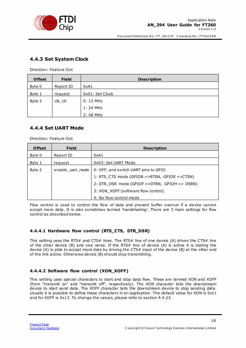
4.4.3 Set System Clock
Direction: Feature Out
Offset Field Description
Byte 0 Report ID 0xA1
Byte 1 request 0x01: Set Clock
Byte 2 clk_ctl 0: 12 MHz
1: 24 MHz
2: 48 MHz
4.4.4 Set UART Mode
Direction: Feature Out
Offset Field Description
Byte 0 Report ID 0xA1
Byte 1 request 0x03: Set UART Mode
Byte 2 enable_uart_mode 0: OFF, and switch UART pins to GPIO
1: RTS_CTS mode (GPIOB =>RTSN, GPIOE =>CTSN)
2: DTR_DSR mode (GPIOF =>DTRN, GPIOH => DSRN)
3: XON_XOFF (software flow control)
4: No flow control mode
Flow control is used to control the flow of data and prevent buffer overrun if a device cannot
accept more data. It is also sometimes termed ‘handshaking’. There are 3 main settings for flow
control as described below.
4.4.4.1 Hardware flow control (RTS_CTS, DTR_DSR)
This setting uses the RTS# and CTS# lines. The RTS# line of one device (A) drives the CTS# line
of the other device (B) and vice versa. If the RTS# line of device (A) is active it is stating the device (A) is able to accept more data by driving the CTS# input of the device (B) at the other end
of the link active. Otherwise device (B) should stop transmitting.
4.4.4.2 Software flow control (XON_XOFF)
This setting uses special characters to start and stop data flow. These are termed XON and XOFF
(from "transmit on" and "transmit off", respectively). The XON character tells the downstream device to start send data. The XOFF character tells the downstream device to stop sending data.
Usually it is possible to define these characters in an application. The default value for XON is 0x11
and for XOFF is 0x13. To change the values, please refer to section 4.4.23.
Application Note
AN_394 User Guide for FT260 V ers ion 1 .0
Document Reference No.: FT_001279 C learance No.: FTDI# 488
19 P roduc t Page
Document Feedback C opyright © Future Technology Devices International Limited
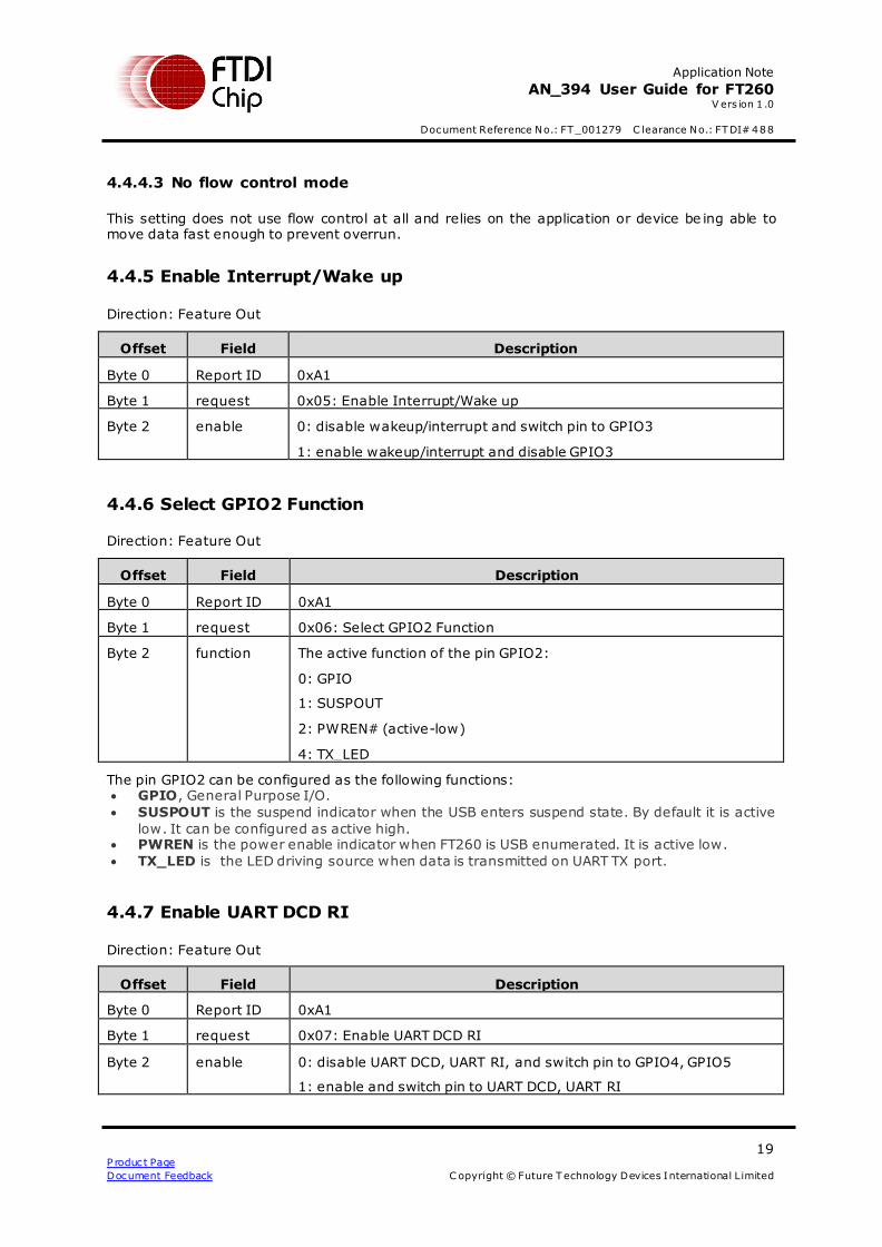
4.4.4.3 No flow control mode
This setting does not use flow control at all and relies on the application or device be ing able to move data fast enough to prevent overrun.
4.4.5 Enable Interrupt/Wake up
Direction: Feature Out
Offset Field Description
Byte 0 Report ID 0xA1
Byte 1 request 0x05: Enable Interrupt/Wake up
Byte 2 enable 0: disable wakeup/interrupt and switch pin to GPIO3
1: enable wakeup/interrupt and disable GPIO3
4.4.6 Select GPIO2 Function
Direction: Feature Out
Offset Field Description
Byte 0 Report ID 0xA1
Byte 1 request 0x06: Select GPIO2 Function
Byte 2 function The active function of the pin GPIO2:
0: GPIO
1: SUSPOUT
2: PWREN# (active-low)
4: TX_LED
The pin GPIO2 can be configured as the following functions: GPIO, General Purpose I/O.
SUSPOUT is the suspend indicator when the USB enters suspend state. By default it is active
low. It can be configured as active high. PWREN is the power enable indicator when FT260 is USB enumerated. It is active low.
TX_LED is the LED driving source when data is transmitted on UART TX port.
4.4.7 Enable UART DCD RI
Direction: Feature Out
Offset Field Description
Byte 0 Report ID 0xA1
Byte 1 request 0x07: Enable UART DCD RI
Byte 2 enable 0: disable UART DCD, UART RI, and switch pin to GPIO4, GPIO5
1: enable and switch pin to UART DCD, UART RI
Application Note
AN_394 User Guide for FT260 V ers ion 1 .0
Document Reference No.: FT_001279 C learance No.: FTDI# 488
20 P roduc t Page
Document Feedback C opyright © Future Technology Devices International Limited
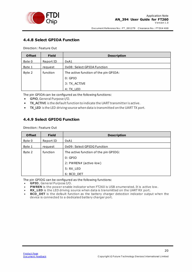
4.4.8 Select GPIOA Function
Direction: Feature Out
Offset Field Description
Byte 0 Report ID 0xA1
Byte 1 request 0x08: Select GPIOA Function
Byte 2 function The active function of the pin GPIOA:
0: GPIO
3: TX_ACTIVE
4: TX_LED
The pin GPIOA can be configured as the following functions:
GPIO, General Purpose I/O. TX_ACTIVE is the default function to indicate the UART transmitter is active.
TX_LED is the LED driving source when data is transmitted on the UART TX port.
4.4.9 Select GPIOG Function
Direction: Feature Out
Offset Field Description
Byte 0 Report ID 0xA1
Byte 1 request 0x09: Select GPIOG Function
Byte 2 function The active function of the pin GPIOG:
0: GPIO
2: PWREN# (active-low)
5: RX_LED
6: BCD_DET
The pin GPIOG can be configured as the following functions: GPIO, General Purpose I/O.
PWREN is the power enable indicator when FT260 is USB enumerated. It is active low. RX_LED is the LED driving source when data is transmitted on the UART RX port.
BCD_DET is the default function as the battery charger detection indicator output when the device is connected to a dedicated battery charger port.
Application Note
AN_394 User Guide for FT260 V ers ion 1 .0
Document Reference No.: FT_001279 C learance No.: FTDI# 488
21 P roduc t Page
Document Feedback C opyright © Future Technology Devices International Limited
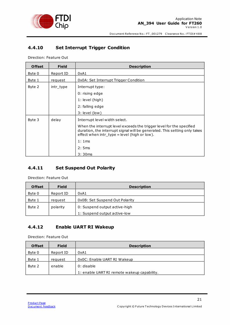
4.4.10 Set Interrupt Trigger Condition
Direction: Feature Out
Offset Field Description
Byte 0 Report ID 0xA1
Byte 1 request 0x0A: Set Interrupt Trigger Condition
Byte 2 intr_type Interrupt type:
0: rising edge
1: level (high)
2: falling edge
3: level (low)
Byte 3 delay Interrupt level width select.
When the interrupt level exceeds the trigger level for the specified
duration, the interrupt signal will be generated. This setting only takes effect when intr_type = level (high or low).
1: 1ms
2: 5ms
3: 30ms
4.4.11 Set Suspend Out Polarity
Direction: Feature Out
Offset Field Description
Byte 0 Report ID 0xA1
Byte 1 request 0x0B: Set Suspend Out Polarity
Byte 2 polarity 0: Suspend output active-high
1: Suspend output active-low
4.4.12 Enable UART RI Wakeup
Direction: Feature Out
Offset Field Description
Byte 0 Report ID 0xA1
Byte 1 request 0x0C: Enable UART RI Wakeup
Byte 2 enable 0: disable
1: enable UART RI remote wakeup capability.
Application Note
AN_394 User Guide for FT260 V ers ion 1 .0
Document Reference No.: FT_001279 C learance No.: FTDI# 488
22 P roduc t Page
Document Feedback C opyright © Future Technology Devices International Limited
4.4.13 Set UART RI Wakeup Config
Direction: Feature Out
Offset Field Description
Byte 0 Report ID 0xA1
Byte 1 request 0x0D: Set UART RI Wakeup Config
Byte 2 config Set UART RI remote wake up type.
0 : rising edge
1 : falling edge (default)
4.4.14 I²C Reset
Direction: Feature Out
Offset Field Description
Byte 0 Report ID 0xA1
Byte 1 request 0x20: I²C Reset
The request will reset the I2C master controller.
4.4.15 Set I²C Clock Speed
Direction: Feature Out
Offset Field Description
Byte 0 Report ID 0xA1
Byte 1 request 0x22: Set I²C Clock Speed
Byte 2 speed_LSB The speed of I2C clock, whose range is from 60K bps to 3400K bps.
Byte 3 speed_MSB
Clock Speed is the frequency of the I²C bus clock in kilohertz (KHz). It’s a two-byte number. For example, if the target clock speed is 100K, the LSB will be 0x64 and the MSB will be 0x00. If the
target clock speed is 1000K (1M), the LSB will be 0xE8 and the MSB will be 0x03. If the given clock speed is not supported, the clock speed will fallback to 100K.
4.4.16 UART Reset
Direction: Feature Out
Offset Field Description
Byte 0 Report ID 0xA1
Byte 1 request 0x40: UART Reset
Application Note
AN_394 User Guide for FT260 V ers ion 1 .0
Document Reference No.: FT_001279 C learance No.: FTDI# 488
23 P roduc t Page
Document Feedback C opyright © Future Technology Devices International Limited
The request will reset the FT260 UART controller.
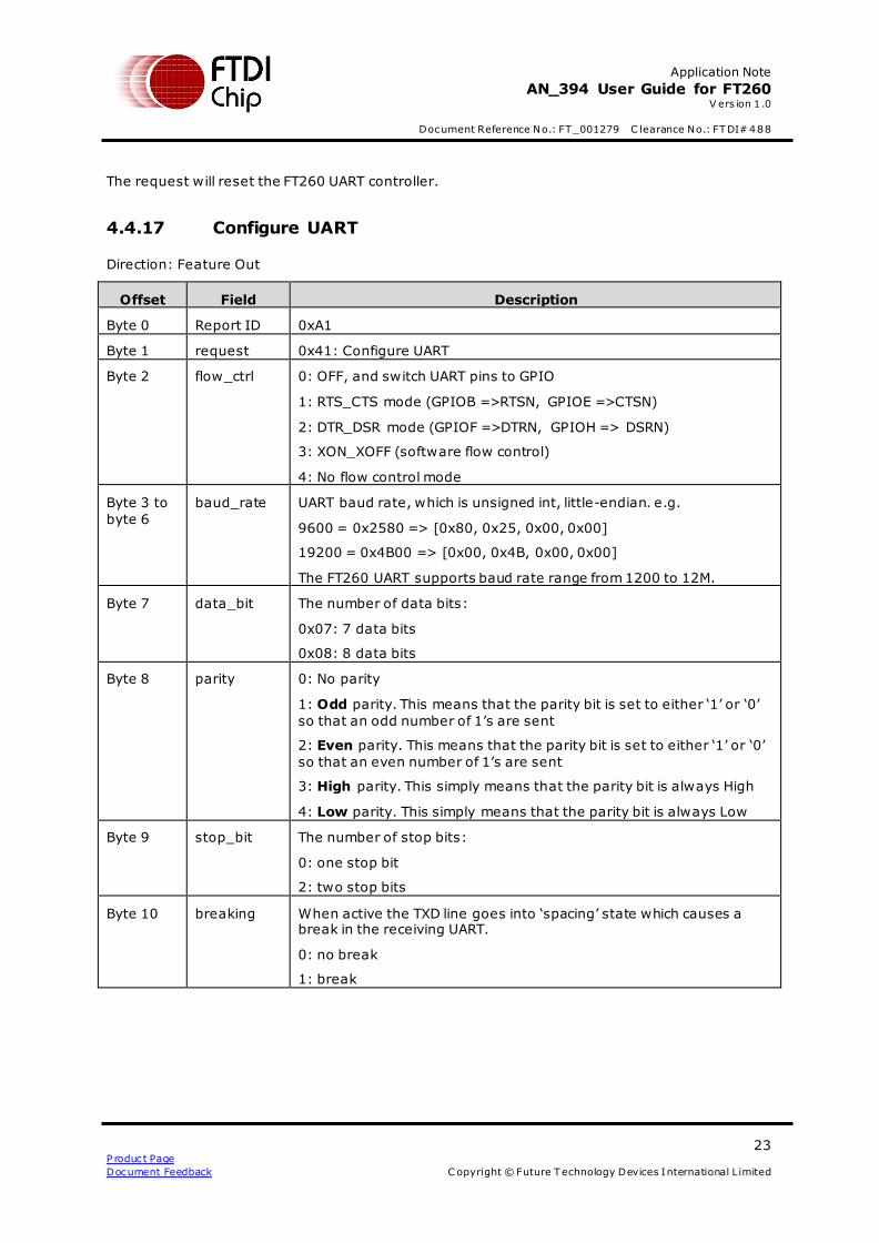
4.4.17 Configure UART
Direction: Feature Out
Offset Field Description
Byte 0 Report ID 0xA1
Byte 1 request 0x41: Configure UART
Byte 2 flow_ctrl 0: OFF, and switch UART pins to GPIO
1: RTS_CTS mode (GPIOB =>RTSN, GPIOE =>CTSN)
2: DTR_DSR mode (GPIOF =>DTRN, GPIOH => DSRN)
3: XON_XOFF (software flow control)
4: No flow control mode
Byte 3 to
byte 6
baud_rate UART baud rate, which is unsigned int, little-endian. e.g.
9600 = 0x2580 => [0x80, 0x25, 0x00, 0x00]
19200 = 0x4B00 => [0x00, 0x4B, 0x00, 0x00]
The FT260 UART supports baud rate range from 1200 to 12M.
Byte 7 data_bit The number of data bits:
0x07: 7 data bits
0x08: 8 data bits
Byte 8 parity 0: No parity
1: Odd parity. This means that the parity bit is set to either ‘1’ or ‘0’
so that an odd number of 1’s are sent
2: Even parity. This means that the parity bit is set to either ‘1’ or ‘0’
so that an even number of 1’s are sent
3: High parity. This simply means that the parity bit is always High
4: Low parity. This simply means that the parity bit is always Low
Byte 9 stop_bit The number of stop bits:
0: one stop bit
2: two stop bits
Byte 10 breaking When active the TXD line goes into ‘spacing’ state which causes a break in the receiving UART.
0: no break
1: break
Application Note
AN_394 User Guide for FT260 V ers ion 1 .0
Document Reference No.: FT_001279 C learance No.: FTDI# 488
24 P roduc t Page
Document Feedback C opyright © Future Technology Devices International Limited
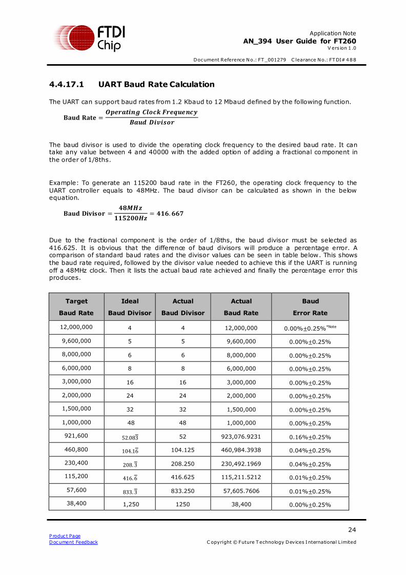
4.4.17.1 UART Baud Rate Calculation
The UART can support baud rates from 1.2 Kbaud to 12 Mbaud defined by the following function.
𝐁𝐚𝐮𝐝 𝐑𝐚𝐭𝐞 =𝑶𝒑𝒆𝒓𝒂𝒕𝒊𝒏𝒈 𝑪𝒍𝒐𝒄𝒌 𝑭𝒓𝒆𝒒𝒖𝒆𝒏𝒄𝒚
𝑩𝒂𝒖𝒅 𝑫𝒊𝒗𝒊𝒔𝒐𝒓
The baud divisor is used to divide the operating clock frequency to the desired baud rate. It can take any value between 4 and 40000 with the added option of adding a fractional component in
the order of 1/8ths.
Example: To generate an 115200 baud rate in the FT260, the operating clock frequency to the
UART controller equals to 48MHz. The baud divisor can be calculated as shown in the below equation.
𝐁𝐚𝐮𝐝 𝐃𝐢𝐯𝐢𝐬𝐨𝐫 =𝟒𝟖𝑴𝑯𝒛
𝟏𝟏𝟓𝟐𝟎𝟎𝑯𝒛= 𝟒𝟏𝟔. 𝟔𝟔𝟕
Due to the fractional component is the order of 1/8ths, the baud divisor must be selected as
416.625. It is obvious that the difference of baud divisors will produce a percentage error. A comparison of standard baud rates and the divisor values can be seen in table below. This shows
the baud rate required, followed by the divisor value needed to achieve this if the UART is running
off a 48MHz clock. Then it lists the actual baud rate achieved and finally the percentage error this produces.
Target
Baud Rate
Ideal
Baud Divisor
Actual
Baud Divisor
Actual
Baud Rate
Baud
Error Rate
12,000,000 4 4 12,000,000 0.00%±0.25%*Note
9,600,000 5 5 9,600,000 0.00%±0.25%
8,000,000 6 6 8,000,000 0.00%±0.25%
6,000,000 8 8 6,000,000 0.00%±0.25%
3,000,000 16 16 3,000,000 0.00%±0.25%
2,000,000 24 24 2,000,000 0.00%±0.25%
1,500,000 32 32 1,500,000 0.00%±0.25%
1,000,000 48 48 1,000,000 0.00%±0.25%
921,600 52.083 52 923,076.9231 0.16%±0.25%
460,800 104.16 104.125 460,984.3938 0.04%±0.25%
230,400 208. 3 208.250 230,492.1969 0.04%±0.25%
115,200 416. 6 416.625 115,211.5212 0.01%±0.25%
57,600 833. 3 833.250 57,605.7606 0.01%±0.25%
38,400 1,250 1250 38,400 0.00%±0.25%
Application Note
AN_394 User Guide for FT260 V ers ion 1 .0
Document Reference No.: FT_001279 C learance No.: FTDI# 488
25 P roduc t Page
Document Feedback C opyright © Future Technology Devices International Limited
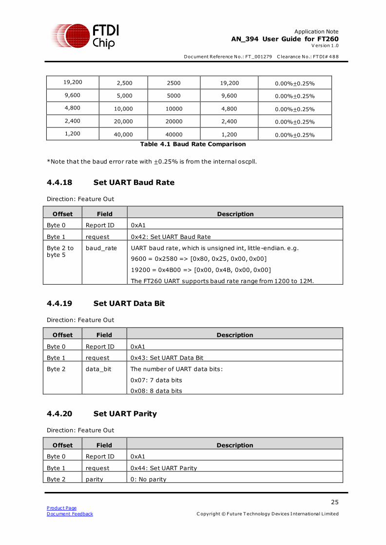
19,200 2,500 2500 19,200 0.00%±0.25%
9,600 5,000 5000 9,600 0.00%±0.25%
4,800 10,000 10000 4,800 0.00%±0.25%
2,400 20,000 20000 2,400 0.00%±0.25%
1,200 40,000 40000 1,200 0.00%±0.25%
Table 4.1 Baud Rate Comparison
*Note that the baud error rate with ±0.25% is from the internal oscpll.
4.4.18 Set UART Baud Rate
Direction: Feature Out
Offset Field Description
Byte 0 Report ID 0xA1
Byte 1 request 0x42: Set UART Baud Rate
Byte 2 to byte 5
baud_rate UART baud rate, which is unsigned int, little-endian. e.g.
9600 = 0x2580 => [0x80, 0x25, 0x00, 0x00]
19200 = 0x4B00 => [0x00, 0x4B, 0x00, 0x00]
The FT260 UART supports baud rate range from 1200 to 12M.
4.4.19 Set UART Data Bit
Direction: Feature Out
Offset Field Description
Byte 0 Report ID 0xA1
Byte 1 request 0x43: Set UART Data Bit
Byte 2 data_bit The number of UART data bits:
0x07: 7 data bits
0x08: 8 data bits
4.4.20 Set UART Parity
Direction: Feature Out
Offset Field Description
Byte 0 Report ID 0xA1
Byte 1 request 0x44: Set UART Parity
Byte 2 parity 0: No parity
Application Note
AN_394 User Guide for FT260 V ers ion 1 .0
Document Reference No.: FT_001279 C learance No.: FTDI# 488
26 P roduc t Page
Document Feedback C opyright © Future Technology Devices International Limited
1: Odd parity. This means that the parity bit is set to either ‘1’ or ‘0’
so that an odd number of 1’s are sent
2: Even parity. This means that the parity bit is set to either ‘1’ or ‘0’
so that an even number of 1’s are sent
3: High parity. This simply means that the parity bit is always High
4: Low parity. This simply means that the parity bit is always Low
4.4.21 Set UART Stop Bit
Direction: Feature Out
Offset Field Description
Byte 0 Report ID 0xA1
Byte 1 request 0x45: Set UART Stop Bit
Byte 2 stop_bit The number of stop bits:
0: one stop bit
2: two stop bits
4.4.22 Set UART Breaking
Direction: Feature Out
Offset Field Description
Byte 0 Report ID 0xA1
Byte 1 request 0x46: Set UART Breaking
Byte 2 breaking When active the TXD line goes into ‘spacing’ state which causes a
break in the receiving UART.
0: no break
1: break
4.4.23 Set UART XON / XOFF
Direction: Feature Out
Offset Field Description
Byte 0 Report ID 0xA1
Byte 1 request 0x49: Set UART XON / XOFF
Byte 2 XON char Character to be used for XON flow control
Byte 3 XOFF char Character to be used for XOFF flow control
Application Note
AN_394 User Guide for FT260 V ers ion 1 .0
Document Reference No.: FT_001279 C learance No.: FTDI# 488
27 P roduc t Page
Document Feedback C opyright © Future Technology Devices International Limited
4.5 I²C
I2C (Inter Integrated Circuit) is a multi-master serial bus invented by Philips. I2C uses two bi-directional open-drain wires called serial data (SDA) and serial clock (SCL). Common I²C bus
speeds are the 100 kbit/s standard mode (SM), 400 kbit/s fast mode (FM), 1 Mbit/s Fast mode
plus (FM+), and 3.4 Mbit/s High Speed mode (HS).
I²C transaction
All I²C transactions begin with a START condition, a slave address, a single bit representing write
(0) or read (1), and are terminated by a STOP condition. All transactions are controlled by the
master.
Sta
rt
7 bit slave address
Read/
Write
AC
K 8 bit data
AC
K 8 bit data
AC
K 8 bit data
AC
K
STO
P
I²C defines three basic types of message:
Single message where a master writes data to a slave; Single message where a master reads data from a slave;
Combined messages, where a master issues at least two reads and/or writes to one or more slaves
For more information on the protocol, refer to the I²C specification.
The FT260 provides flexibility to allow users to decide when to send START and STOP conditions.
Here are some examples. The following scenarios are supported by the FT260.
Send data with START_AND_STOP conditions
Sta
rt 7 bit slave address
write
AC
K 8 bit data
AC
K 8 bit data
AC
K 8 bit data
AC
K
STO
P
Send the first packet with START condition, and then send remaining data in the other packet with
STOP condition.
Sta
rt
7 bit slave address
write
AC
K 8 bit data
AC
K
8 bit data
AC
K 8 bit data
AC
K
STO
P
Separate data into three packets.
Sta
rt
7 bit slave
address
write
AC
K
8 bit data
AC
K
8 bit data
AC
K 8 bit data
AC
K
8 bit data
AC
K
STO
P
Application Note
AN_394 User Guide for FT260 V ers ion 1 .0
Document Reference No.: FT_001279 C learance No.: FTDI# 488
28 P roduc t Page
Document Feedback C opyright © Future Technology Devices International Limited
I²C combined message
In a combined message, each read or write begins with a START and the slave address. After the
first START, these are also called repeated START bits; repeated START bits are not preceded by
STOP bits, which is how slaves know the next transfer is part of the same message.
Sta
rt
7 bit slave address
write
AC
K 8 bit data
AC
K
SR
7 bit slave address
read
AC
K
8 bit data
AC
K
8 bit data
AC
K
STO
P
SR = repeated START condition
4.5.1 Get I²C Status
Direction: Feature In
Offset Field Description
Byte 0 Report ID 0xC0
Byte 1 bus status I2C bus status:
bit 0 = controller busy: all other status bits invalid
bit 1 = error condition bit 2 = slave address was not acknowledged during last
operation
bit 3 = data not acknowledged during last operation
bit 4 = arbitration lost during last operation bit 5 = controller idle
bit 6 = bus busy
Byte 2 speed_LSB The speed of I2C transmission. It ranges from 60K bps to 3400K bps.
Clock Speed is the frequency of the I²C bus clock in kilohertz (kHz).
It’s a two-byte number
Byte 3 speed_MSB
Byte 4 reserved reserved
Application Note
AN_394 User Guide for FT260 V ers ion 1 .0
Document Reference No.: FT_001279 C learance No.: FTDI# 488
29 P roduc t Page
Document Feedback C opyright © Future Technology Devices International Limited
4.5.2 I²C Write Request
Direction: Interrupt Out
Offset Field Description
Byte 0 Report ID 0xD0 – 0xDE
The report ID determines the length of the data payload, in multiples
of 4 bytes.
0xD0 : maximum data size is 4 bytes
0xD1 : maximum data size is 8 bytes
0xD2 : maximum data size is 12 bytes
...
0xDE : maximum data size is 60 bytes
Byte 1 slaveAddr The address (7-bit) of the I²C slave device
Byte 2 flag The I²C condition to be sent with this I2C transaction:
0: None 0x02: START
0x03: Repeated_START Repeated_START will not send master code in HS mode
0x04: STOP 0x06: START_AND_STOP
Byte 3 length The length of valid data of payload.
Byte 4 to
Byte 63
data The data payload.
The maximum size of the data payload is determined by the report ID: (Report ID - 0xD0 + 1) * 4
Maximum Data Payload Size
The packet size of a HID report is fixed, the FT260 defines a series of report IDs for sending I²C
write request with different packet size.
For example, the report ID 0xDE defines a 64 bytes packet, which is composed of 4 bytes header and 60 bytes data payload.
If the data is larger than 60 bytes, it cannot be sent in one packet. The data must be divided and sent in continuous packets.
However, if the data to be sent is only a few bytes, 60 bytes payload seems wasteful.
The FT260 defines a series of report IDs with data payload sizes in multiples of 4. Starting from report ID 0xD0, which defines 4 bytes data payload, the next report ID 0xD1 defines 8 bytes data
payload, until report ID 0xDE which defines 60 bytes data payload.
Application Note
AN_394 User Guide for FT260 V ers ion 1 .0
Document Reference No.: FT_001279 C learance No.: FTDI# 488
30 P roduc t Page
Document Feedback C opyright © Future Technology Devices International Limited
The length field indicates the number of valid bytes in the data payload. For example, if you have
5 bytes to send, you can choose report ID 0xD1, which has 8 bytes payload, and set the length field to 5.
4.5.3 I²C Read Request
Direction: Interrupt Out
Offset Field Description
Byte 0 Report ID 0xC2
Byte 1 slaveAddr The address (7-bit) of the I²C slave device
Byte 2 flag The I2C condition will be sent with this I2C transaction
0: None
0x02: START 0x03: Repeated_START
Repeated_START will not send master code in HS mode
0x04: STOP
0x06: START_AND_STOP
Byte 3
and byte 4
length The number of bytes requested from the slave device.
The byte order is little endian.
Reading data from an I²C slave device will be completed in two steps:
1. Send an I²C read request. 2. Receive data in one or more I²C input reports.
After receiving the read request, the FT260 I²C master controller will query data from the given slave, and send the data back to the host via interrupt in and I²C input reports.
4.5.4 I²C Input Report
Direction: Interrupt In
Offset Field Description
Byte 0 Report ID 0xD0 – 0xDE
The actual value depends on the length of the data payload.
Byte 1 length The length of valid data of payload.
Byte 2 to
Byte 63
data The data payload
The FT260 will send the data from an I²C slave back to the host via the I²C input reports when it
receives an I²C read request. As with the write request, the different report IDs define different packet sizes. For input requests, application code may ignore the report ID, but must check the
length field to get the valid data size.
Application Note
AN_394 User Guide for FT260 V ers ion 1 .0
Document Reference No.: FT_001279 C learance No.: FTDI# 488
31 P roduc t Page
Document Feedback C opyright © Future Technology Devices International Limited
4.6 UART
UART (Universal Asynchronous Receiver/Transmitter) is a commonly used interface to transfer serial data. Being asynchronous there is no clock signal but the structure of the transmitted data
provides for a start and an end to a message. It is also important that both ends of the link decide
to operate with the same pulse width defined as the baud rate. The UART of a micro-controller will normally operate at 3V3 or 5V TTL levels. The UART will only connect to one other device in the
chain.
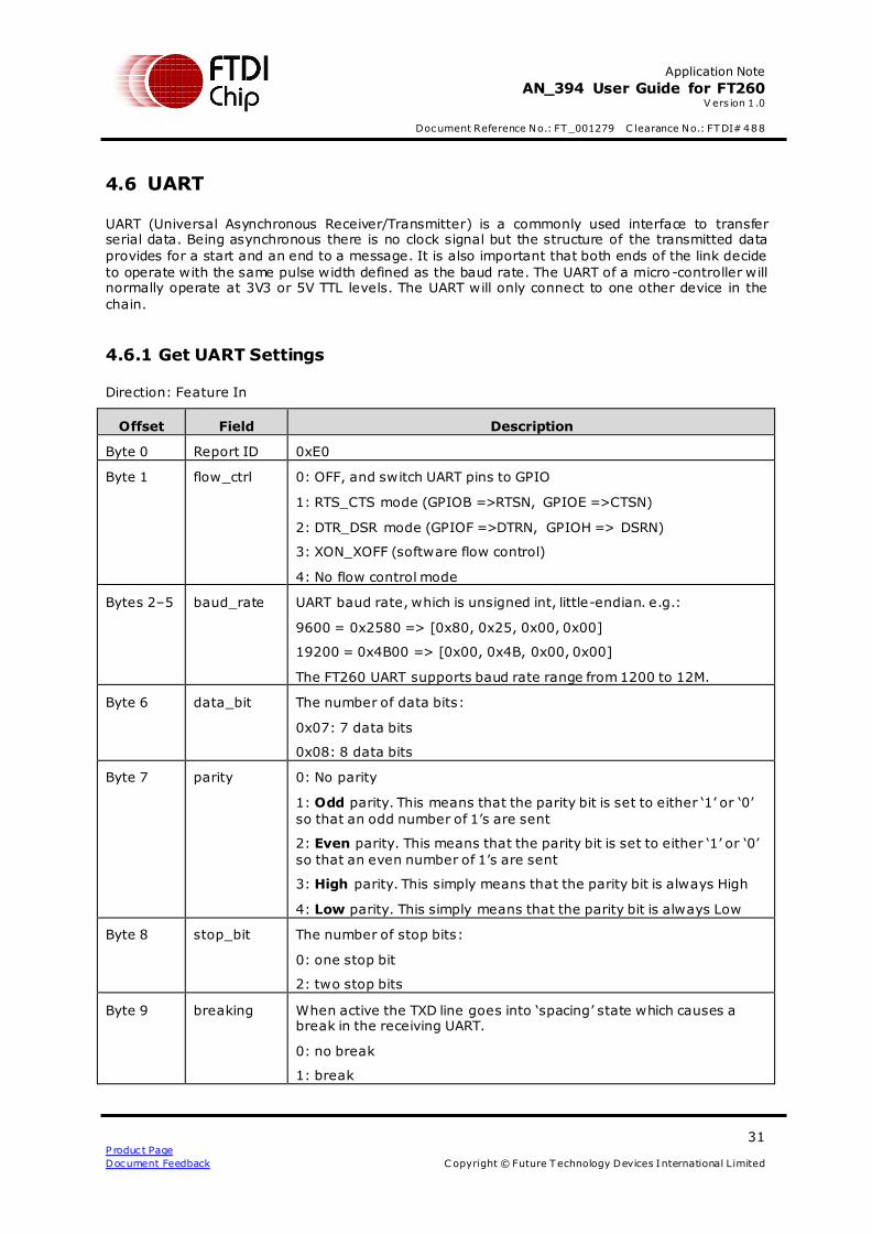
4.6.1 Get UART Settings
Direction: Feature In
Offset Field Description
Byte 0 Report ID 0xE0
Byte 1 flow_ctrl 0: OFF, and switch UART pins to GPIO
1: RTS_CTS mode (GPIOB =>RTSN, GPIOE =>CTSN)
2: DTR_DSR mode (GPIOF =>DTRN, GPIOH => DSRN)
3: XON_XOFF (software flow control)
4: No flow control mode
Bytes 2–5 baud_rate UART baud rate, which is unsigned int, little-endian. e.g.:
9600 = 0x2580 => [0x80, 0x25, 0x00, 0x00]
19200 = 0x4B00 => [0x00, 0x4B, 0x00, 0x00]
The FT260 UART supports baud rate range from 1200 to 12M.
Byte 6 data_bit The number of data bits:
0x07: 7 data bits
0x08: 8 data bits
Byte 7 parity 0: No parity
1: Odd parity. This means that the parity bit is set to either ‘1’ or ‘0’
so that an odd number of 1’s are sent
2: Even parity. This means that the parity bit is set to either ‘1’ or ‘0’
so that an even number of 1’s are sent
3: High parity. This simply means that the parity bit is always High
4: Low parity. This simply means that the parity bit is always Low
Byte 8 stop_bit The number of stop bits:
0: one stop bit
2: two stop bits
Byte 9 breaking When active the TXD line goes into ‘spacing’ state which causes a break in the receiving UART.
0: no break
1: break
Application Note
AN_394 User Guide for FT260 V ers ion 1 .0
Document Reference No.: FT_001279 C learance No.: FTDI# 488
32 P roduc t Page
Document Feedback C opyright © Future Technology Devices International Limited
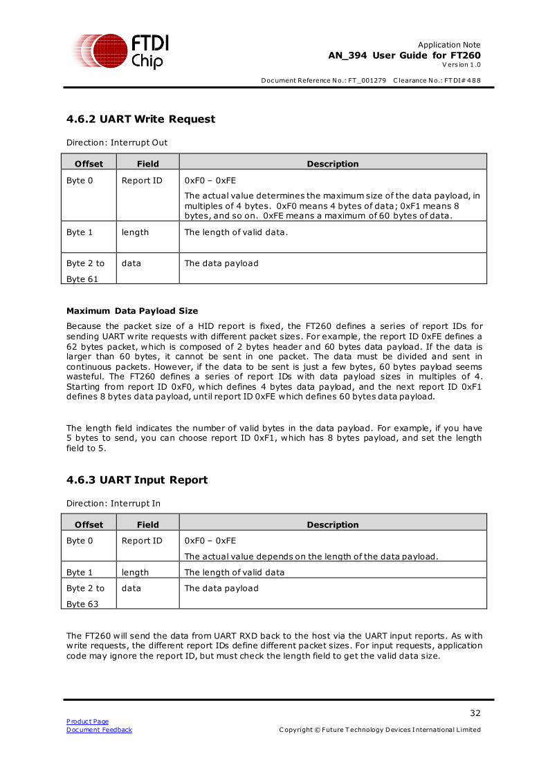
4.6.2 UART Write Request
Direction: Interrupt Out
Offset Field Description
Byte 0 Report ID 0xF0 – 0xFE
The actual value determines the maximum size of the data payload, in
multiples of 4 bytes. 0xF0 means 4 bytes of data; 0xF1 means 8 bytes, and so on. 0xFE means a maximum of 60 bytes of data.
Byte 1 length The length of valid data.
Byte 2 to
Byte 61
data The data payload
Maximum Data Payload Size
Because the packet size of a HID report is fixed, the FT260 defines a series of report IDs for
sending UART write requests with different packet sizes. For example, the report ID 0xFE defines a
62 bytes packet, which is composed of 2 bytes header and 60 bytes data payload. If the data is larger than 60 bytes, it cannot be sent in one packet. The data must be divided and sent in
continuous packets. However, if the data to be sent is just a few bytes, 60 bytes payload seems wasteful. The FT260 defines a series of report IDs with data payload sizes in multiples of 4.
Starting from report ID 0xF0, which defines 4 bytes data payload, and the next report ID 0xF1 defines 8 bytes data payload, until report ID 0xFE which defines 60 bytes data payload.
The length field indicates the number of valid bytes in the data payload. For example, if you have 5 bytes to send, you can choose report ID 0xF1, which has 8 bytes payload, and set the length
field to 5.
4.6.3 UART Input Report
Direction: Interrupt In
Offset Field Description
Byte 0 Report ID 0xF0 – 0xFE
The actual value depends on the length of the data payload.
Byte 1 length The length of valid data
Byte 2 to
Byte 63
data The data payload
The FT260 will send the data from UART RXD back to the host via the UART input reports. As with write requests, the different report IDs define different packet sizes. For input requests, application
code may ignore the report ID, but must check the length field to get the valid data size.
Application Note
AN_394 User Guide for FT260 V ers ion 1 .0
Document Reference No.: FT_001279 C learance No.: FTDI# 488
33 P roduc t Page
Document Feedback C opyright © Future Technology Devices International Limited
4.6.4 Get DCD & RI Status
Direction: Feature In
Offset Field Description
Byte 0 Report ID 0xE2
Byte 1 status Bit0 : status of UART DCD
Bit1 : status of UART RI
4.7 GPIO
4.7.1 GPIO Write Request
Direction: Feature Out
Offset Field Description
Byte 0 Report ID 0xB0
Byte 1 gpio value GPIO0–5 values
GPIO0: bit[0], GPIO1: bit[1], GPIO2: bit[2], GPIO3: bit[3],
GPIO2: bit[4], GPIO3: bit[5]
Byte 2 gpio dir GPIO0–5 directions:
0b: input
1b: output
Byte 3 gpioEx
value
GPIOA–H values
GPIOA: bit[0], GPIOB: bit[1], GPIOC: bit[2], GPIOD: bit[3],
GPIOE: bit[4], GPIOF: bit[5], GPIOG: bit[6], GPIOH: bit[7]
Byte 4 gpioEx dir GPIOA–H directions:
0b: input
1b: output
4.7.2 GPIO Read Request
Direction: Feature In
Offset Field Description
Byte 0 Report ID 0xB0
Byte 1 gpio value GPIO0–5 values:
GPIO0: bit[0], GPIO1: bit[1], GPIO2: bit[2], GPIO3: bit[3],
GPIO2: bit[4], GPIO3: bit[5]
Byte 2 gpio dir GPIO0–5 directions:
0b: input
Application Note
AN_394 User Guide for FT260 V ers ion 1 .0
Document Reference No.: FT_001279 C learance No.: FTDI# 488
34 P roduc t Page
Document Feedback C opyright © Future Technology Devices International Limited
1b: output
Byte 3 gpioEx
value
GPIOA–H values:
GPIOA: bit[0], GPIOB: bit[1], GPIOC: bit[2], GPIOD: bit[3],
GPIOE: bit[4], GPIOF: bit[5], GPIOG: bit[6], GPIOH: bit[7]
Byte 4 gpioEx dir GPIOA–H directions:
0b: input
1b: output
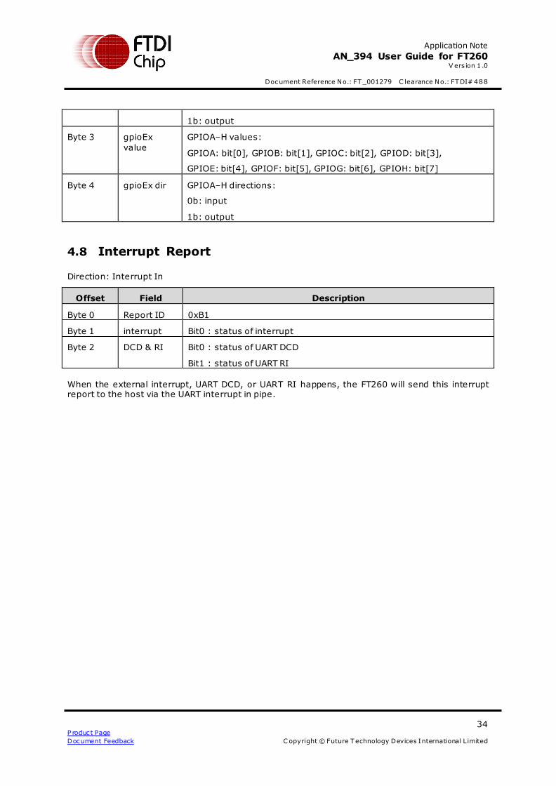
4.8 Interrupt Report
Direction: Interrupt In
Offset Field Description
Byte 0 Report ID 0xB1
Byte 1 interrupt Bit0 : status of interrupt
Byte 2 DCD & RI Bit0 : status of UART DCD
Bit1 : status of UART RI
When the external interrupt, UART DCD, or UART RI happens, the FT260 will send this interrupt report to the host via the UART interrupt in pipe.
Application Note
AN_394 User Guide for FT260 V ers ion 1 .0
Document Reference No.: FT_001279 C learance No.: FTDI# 488
35 P roduc t Page
Document Feedback C opyright © Future Technology Devices International Limited
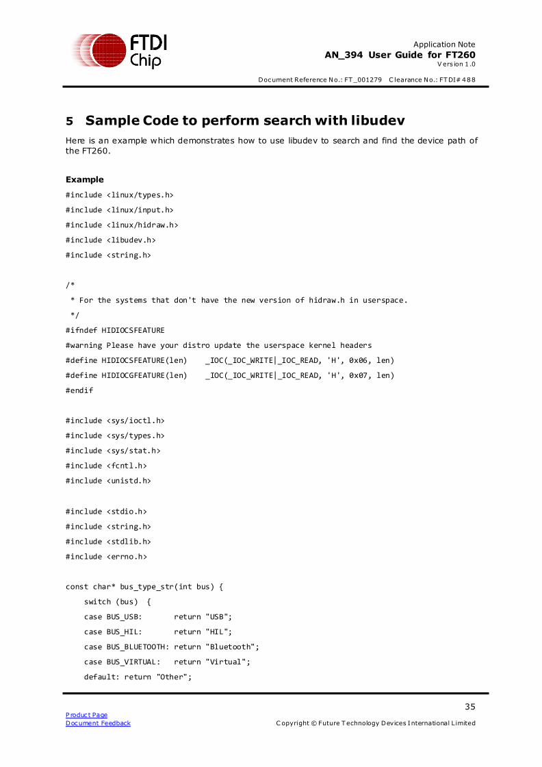
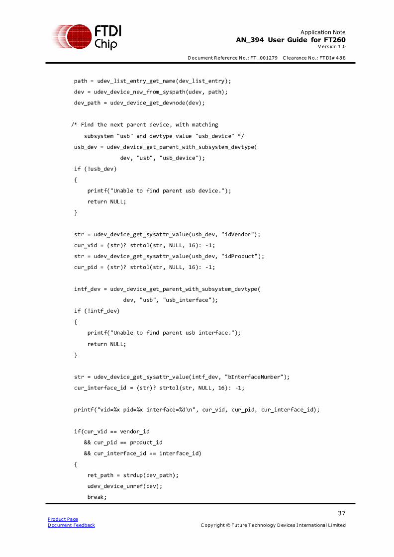
5 Sample Code to perform search with libudev
Here is an example which demonstrates how to use libudev to search and find the device path of
the FT260.
Example
#include <linux/types.h>
#include <linux/input.h>
#include <linux/hidraw.h>
#include <libudev.h>
#include <string.h>
/*
* For the systems that don't have the new version of hidraw.h in userspace.
*/
#ifndef HIDIOCSFEATURE
#warning Please have your distro update the userspace kernel headers
#define HIDIOCSFEATURE(len) _IOC(_IOC_WRITE|_IOC_READ, 'H', 0x06, len)
#define HIDIOCGFEATURE(len) _IOC(_IOC_WRITE|_IOC_READ, 'H', 0x07, len)
#endif
#include <sys/ioctl.h>
#include <sys/types.h>
#include <sys/stat.h>
#include <fcntl.h>
#include <unistd.h>
#include <stdio.h>
#include <string.h>
#include <stdlib.h>
#include <errno.h>
const char* bus_type_str(int bus) {
switch (bus) {
case BUS_USB: return "USB";
case BUS_HIL: return "HIL";
case BUS_BLUETOOTH: return "Bluetooth";
case BUS_VIRTUAL: return "Virtual";
default: return "Other";
Application Note
AN_394 User Guide for FT260 V ers ion 1 .0
Document Reference No.: FT_001279 C learance No.: FTDI# 488
36 P roduc t Page
Document Feedback C opyright © Future Technology Devices International Limited
}
}
char* get_hid_path(unsigned short vendor_id, unsigned short product_id, unsigned short interface_id)
{
struct udev* udev;
struct udev_enumerate* enumerate;
struct udev_list_entry *devices, *dev_list_entry;
struct udev_device* dev;
struct udev_device* usb_dev;
struct udev_device* intf_dev;
char* ret_path = NULL;
/* Create the udev object */
udev = udev_new();
if (!udev)
{
printf("Can't create udev\n");
return NULL;
}
/* Create a list of the devices in the 'hidraw' subsystem. */
enumerate = udev_enumerate_new(udev);
udev_enumerate_add_match_subsystem(enumerate, "hidraw");
udev_enumerate_scan_devices(enumerate);
devices = udev_enumerate_get_list_entry(enumerate);
/* udev_list_entry_foreach is a macro which expands to a loop. */
udev_list_entry_foreach(dev_list_entry, devices)
{
const char* path;
const char* dev_path;
const char* str;
unsigned short cur_vid;
unsigned short cur_pid;
unsigned short cur_interface_id;
Application Note
AN_394 User Guide for FT260 V ers ion 1 .0
Document Reference No.: FT_001279 C learance No.: FTDI# 488
37 P roduc t Page
Document Feedback C opyright © Future Technology Devices International Limited
path = udev_list_entry_get_name(dev_list_entry);
dev = udev_device_new_from_syspath(udev, path);
dev_path = udev_device_get_devnode(dev);
/* Find the next parent device, with matching
subsystem "usb" and devtype value "usb_device" */
usb_dev = udev_device_get_parent_with_subsystem_devtype(
dev, "usb", "usb_device");
if (!usb_dev)
{
printf("Unable to find parent usb device.");
return NULL;
}
str = udev_device_get_sysattr_value(usb_dev, "idVendor");
cur_vid = (str)? strtol(str, NULL, 16): -1;
str = udev_device_get_sysattr_value(usb_dev, "idProduct");
cur_pid = (str)? strtol(str, NULL, 16): -1;
intf_dev = udev_device_get_parent_with_subsystem_devtype(
dev, "usb", "usb_interface");
if (!intf_dev)
{
printf("Unable to find parent usb interface.");
return NULL;
}
str = udev_device_get_sysattr_value(intf_dev, "bInterfaceNumber");
cur_interface_id = (str)? strtol(str, NULL, 16): -1;
printf("vid=%x pid=%x interface=%d\n", cur_vid, cur_pid, cur_interface_id);
if(cur_vid == vendor_id
&& cur_pid == product_id
&& cur_interface_id == interface_id)
{
ret_path = strdup(dev_path);
udev_device_unref(dev);
break;
Application Note
AN_394 User Guide for FT260 V ers ion 1 .0
Document Reference No.: FT_001279 C learance No.: FTDI# 488
38 P roduc t Page
Document Feedback C opyright © Future Technology Devices International Limited
}
udev_device_unref(dev);
}
/* Free the enumerator object */
udev_enumerate_unref(enumerate);
udev_unref(udev);
return ret_path;
}
int main(int argc, char** argv)
{
int fd;
int res, desc_size = 0;
char buf[256];
struct hidraw_report_descriptor rpt_desc;
struct hidraw_devinfo info;
char* device_path = NULL;
if (argc > 1)
{
device_path = malloc(100);
strcpy(device_path, argv[1]);
}
else
{
/* remember to free device_path */
device_path = get_hid_path(0x0403, 0x6030, 0);
}
if(!device_path)
{
perror("Can not find the device path");
return 1;
}
/* Open the Device with non-blocking reads. */
Application Note
AN_394 User Guide for FT260 V ers ion 1 .0
Document Reference No.: FT_001279 C learance No.: FTDI# 488
39 P roduc t Page
Document Feedback C opyright © Future Technology Devices International Limited
fd = open(device, O_RDWR|O_NONBLOCK);
if (fd < 0) {
perror("Unable to open device");
return 1;
}
memset(&rpt_desc, 0x0, sizeof(rpt_desc));
memset(&info, 0x0, sizeof(info));
memset(buf, 0x0, sizeof(buf));
/* Get Report Descriptor Size */
res = ioctl(fd, HIDIOCGRDESCSIZE, &desc_size);
if (res < 0) {
perror("HIDIOCGRDESCSIZE");
} else {
printf("Report Descriptor Size: %d\n", desc_size);
}
/* Get Raw Name */
res = ioctl(fd, HIDIOCGRAWNAME(256), buf);
if (res < 0) {
perror("HIDIOCGRAWNAME");
} else {
printf("Raw Name: %s\n", buf);
}
/* Get Raw Info */
res = ioctl(fd, HIDIOCGRAWINFO, &info);
if (res < 0) {
perror("HIDIOCGRAWINFO");
} else {
printf("Raw Info:\n");
printf("\tbustype: %d (%s)\n",
info.bustype, bus_type_str(info.bustype));
printf("\tvendor: 0x%04hx\n", info.vendor);
printf("\tproduct: 0x%04hx\n", info.product);
}
Application Note
AN_394 User Guide for FT260 V ers ion 1 .0
Document Reference No.: FT_001279 C learance No.: FTDI# 488
40 P roduc t Page
Document Feedback C opyright © Future Technology Devices International Limited
/* Set Feature */
buf[0] = 0xA1; /* SYSTEM_SETTING_ID */
buf[1] = 0x22; /* I2C_SPEED */
buf[2] = 0x01; /* 400Kbps */
buf[3] = 0x90;
res = ioctl(fd, HIDIOCSFEATURE(4), buf);
if (res < 0) {
perror("HIDIOCSFEATURE");
} else {
printf("ioctl HIDIOCGFEATURE returned: %d\n", res);
}
/* Send a Report to the Device */
buf[0] = 0xD0; /* I2C write */
buf[1] = 0x22; /* Slave address */
buf[2] = 0x06; /* Start and Stop */
buf[3] = 0x03; /* data len */
buf[4] = 'a';
buf[5] = 'b';
buf[6] = 'c';
res = write(fd, buf, 7);
if (res < 0) {
printf("Error: %d\n", errno);
perror("write");
} else {
printf("write() wrote %d bytes\n", res);
}
free(device_path);
close(fd);
return 0;
}
Application Note
AN_394 User Guide for FT260 V ers ion 1 .0
Document Reference No.: FT_001279 C learance No.: FTDI# 488
41 P roduc t Page
Document Feedback C opyright © Future Technology Devices International Limited
6 Contact Information
Head Office – Glasgow, UK Future Technology Devices International Limited Unit 1, 2 Seaward Place, Centurion Business Park Glasgow G41 1HH United Kingdom Tel: +44 (0) 141 429 2777 Fax: +44 (0) 141 429 2758 E-mail (Sales) [email protected] E-mail (Support) [email protected] E-mail (General Enquiries) [email protected]
Branch Office – Taipei, Taiwan Future Technology Devices International Limited (Taiwan) 2F, No. 516, Sec. 1, NeiHu Road Taipei 114 Taiwan , R.O.C. Tel: +886 (0) 2 8791 3570 Fax: +886 (0) 2 8791 3576 E-mail (Sales) [email protected] E-mail (Support) [email protected] E-mail (General Enquiries) [email protected]
Branch Office – Tigard, Oregon, USA Future Technology Devices International Limited (USA) 7130 SW Fir Loop Tigard, OR 97223-8160 USA Tel: +1 (503) 547 0988 Fax: +1 (503) 547 0987 E-Mail (Sales) [email protected] E-Mail (Support) [email protected] E-Mail (General Enquiries) [email protected]
Branch Office – Shanghai, China Future Technology Devices International Limited (China) Room 1103, No. 666 West Huaihai Road, Shanghai, 200052 China Tel: +86 21 62351596 Fax: +86 21 62351595 E-mail (Sales) [email protected] E-mail (Support) [email protected] E-mail (General Enquiries) [email protected]
Web Site http://ftdichip.com
Distributor and Sales Representatives
Please visit the Sales Network page of the FTDI Web site for the contact details of our distributor(s) and sales representative(s) in your country.
System and equipment manufacturers and designers are responsible to ensure that their systems, and any Future Technology
Devices International Ltd (FTDI) devices incorporated in their sys tems, meet all applicable safety, regulatory and system-level
performance requirements . A ll application-related information in this document (inc luding application descriptions , sugges ted
FTDI devices and other materials ) is provided for reference only. While FTDI has taken care to assure it is accurate, this
information is subjec t to cus tomer confirmation, and FTDI disclaims all liability for sys tem des igns and for any applications
ass istance provided by FTDI. Use of FTDI devices in life support and/or safety applications is entirely at the user’s risk, and the
user agrees to defend, indemnify and hold harmless FTDI from any and all damages , c laims , suits or expense resulting from
such use. This document is subject to change without notice. No freedom to use patents or other intellec tual property rights is
implied by the publication of this document. Neither the whole nor any part of the information contained in, or the produc t
desc ribed in this document, may be adapted or reproduc ed in any material or electronic form without the prior written consent
of the copyright holder. Future Technology Devices International Ltd, Unit 1 , 2 Seaward P lace, Centurion Business Park,
Glasgow G41 1HH, United Kingdom. Scotland Registered C ompany Number: SC136640
42 P roduc t Page
Document Feedback C opyright © Future Technology Devices International Limited
Appendix A – References
Document References
DS_FT260
Acronyms and Abbreviations
Terms Description
GPIO General-purpose input/output
HID Human Interface Device
I2C Inter-Integrated Circuit
UART Universal Asynchronous Receiver/Transmitter
USB Universal Serial Bus
USB-IF USB Implementers Forum
Application Note
AN_394 User Guide for FT260 V ers ion 1 .0
Document Reference No.: FT_001279 C learance No.: FTDI# 488
43 P roduc t Page
Document Feedback C opyright © Future Technology Devices International Limited
Appendix B – List of Tables & Figures
List of Tables
Table 1.1 FT260 interface configuration ........................................................................................ 6
Table 1.2 FT260 endpoints ........................................................................................................... 6
Table 4.1 Baud Rate Comparison ................................................................................................ 25
List of Figures
Figure 1.1 The FT260 System Block Diagram ................................................................................ 5
Figure 2.1 The FT260 connects with I²C bus ................................................................................. 8
Figure 2.2 The FT260 connects to an UART device ........................................................................ 9
Application Note
AN_394 User Guide for FT260 V ers ion 1 .0
Document Reference No.: FT_001279 C learance No.: FTDI# 488
44 P roduc t Page
Document Feedback C opyright © Future Technology Devices International Limited
Appendix C – Revision History
Document Title: AN_394 User Guide for FT260
Document Reference No.: FT_001279
Clearance No.: FTDI# 488
Product Page: http://www.ftdichip.com/FTProducts.htm
Document Feedback: Send Feedback
Revision Changes Date
1.0 Initial Release 2016-03-08