Embed Size (px)
Citation preview

User’s Manua- Model #MFC2005S-UN30C
WINSONIC ELECTRONICS Co., LTD No.290-1, Wen Chung Rd., Taoyuan City, Taiwan, R.O.C
l:+886-3-3704789 ax:+886-3-3704722
E-mail:[email protected] www.ewinsonic.com
TeF
AD Board Specification
Panel Specification
Safety InstructionProduct Installation
Contents
General Description
Optical Specifications
Absolute Maximum Ratings
Electrical Specifications
AssemblyTrouble Shooting
345
31
5
29
6721
26
3839
Mechanical Characteristics
PRECAUTIONS

Safety Instruction
Read and follow these instructions when connecting and using your LCD monitor: Operation:
1. Keep the monitor out of direct sunlight and away from stoves or any other heat source.
2. Remove any object that could fall into ventilation holes or prevent proper cooling of the monitor's electronics.
3. Do not block the ventilation holes on the cabinet. 4. When positioning the monitor, make sure the power plug and outlet are easily
accessible. 5. If turning off the monitor by detaching the power cable or DC power cord, wait
for seconds before attaching the power cable or DC power cord for normal operation.
6. Do not subject the LCD monitor to severe vibration or high impact conditions during operation.
7. Do not knock or drop the monitor during operation or transportation. Maintenance:
8. To protect your display from possible damage, do not put excessive pressure on the LCD panel. When moving your monitor, grasp the frame to lift; do not lift the monitor by placing your hand or fingers on the LCD panel.
9. Unplug the monitor if you are not going to use it for an extensive period of time. 10. Unplug the monitor if you need to clean it with a slightly damp cloth. The screen
may be wiped with a dry cloth when the power is off. However, never use organic solvent, such as, alcohol, or ammonia-based liquids to clean your monitor.
11. To avoid the risk of shock or permanent damage to the set, do not expose the monitor to dust, rain, water, or excessive moisture environment.
12. If your monitor gets wet, wipe it with dry cloth as soon as possible. 13. If foreign substance or water gets in your monitor, please turn the power off
immediately and disconnect the power cord. Then, remove the foreign substance or water, and send it to the maintenance center.
14. Do not store or use the LCD monitor in locations exposed to heat, direct sunlight or extreme cold.
15. In order to maintain the best performance of your monitor and use it for a longer lifetime, please use the monitor in a location that falls within the following temperature and humidity ranges. Temperature: 5-35°C 41-95°F

Product Installation
1. Switch off the power on both your monitor and your computer. The Power Switch is located in the right of the monitor.
2. Connect the power cord to the AC outlet, and connect the power to the monitor through the AC/DC adapter.
3. VGA Signal-Plug one end of the 15-pin signal cable to the video signal connector at the rear of the PC system and the other end to the monitor. Secure the connectors with the screws on the cable connector at both ends.
4. (Optional) DVI Signal-Plug one end of the DVI signal cable to the video signal connector at the rear of the PC system and the other end to the monitor. Secure the connectors with the screws on the cable connector at both ends.
5. (Optional) HDMI Signal-Plug one end of the HDMI signal cable to the video signal connector at the rear of the PC system and the other end to the monitor. Secure the connectors with the screws on the cable connector at both ends.
6. (Optional) RS232 Connection- Plug one end of RS232 cable to com-port connector on your PC system and the other end to the monitor. Secure the connectors with the screws on the cable connector at both ends.

Panel Specification
1. General Description
MFC2005S-UN30C is a Color Active Matrix Liquid Crystal Display with an integral Cold Cathode FluorescentLamp(CCFL) backlight system. The matrix employs a-Si Thin Film Transistor as the active element.It is a transmissive type display operating in the normally black mode. It has a 20.1 inch diagonally measured act ive display area with UXGA resolution (1200 vert ical by 1600 horizontal pixel ar ray)Each pixel is divided into Red, Green and Blue sub-pixels or dots which are arranged in vertical stripes.Gray scale or the brightness of the sub-pixel color is determined with a 8-bit gray scale signal for each dot,thus, presenting a palette of more than 16,7M(True) colors. It has been designed to apply the 8Bit 2 port LVDS interface.I t i s in tended to suppor t d isp lays where h igh br ightness, super w ide v iewing angle,high color saturation, and high color are important.
General FeaturesActive Screen Size 20.1 inches(510.54mm) diagonal
Outline Dimension 432.0(H) x 331.5(V) x 25.0(D) mm(Typ.)
Pixel Pitch 0.255mm x 0.255mm
Pixel Format 1600 horizontal By 1200 vertical Pixels RGB stripe arrangement
Color Depth 8bit, 16,7 M colors
Viewing Angle (CR>10) Viewing Angle Free ( R/L 178(Typ.), U/D 178(Typ) )
Luminance, White 300 cd/m2 (Center 1 point, Typ.)
Power Consumption Total 35.38 Watt(Typ.) (5.98 Watt@VLCD, 29.4 Watt@300cd/[LAMP=7mA])
Weight 3200 g (Typ.)
Display Operating Mode Transmissive mode, normally black
Surface Treatment Hard coating (3H), Anti-glare treatment of the front polarizer
TFT-LCD Panel(1600 × 1200 pixels)
Source Driver CircuitTiming Control
Block
Power Circuit Block
CN1(30pin)
Backlight Assembly(6 CCFL)
RGB, Dclk, DEHsync, Vsync(LVDS 2 port)
VLCD(+18V)
G1200
G1
S1600S1
Gate D
river circuit
CN2(5PIN), 3(2PIN)
CN4(2PIN), 5(5PIN)
VLamp
VLamp

Panel Specification
2. Absolute Maximum Ratings
The following are maximum values which, if exceeded, may cause faulty operation or damage to the unit.
Table 1. ABSOLUTE MAXIMUM RATINGS
Note : 1. Temperature and relative humidity range are shown in the figure below. Wet bulb temperature should be 39 °C Max, and no condensation of water.
ValuesParameter
Min MaxUnits
Power Input Voltage VLCD -0.3 23.0 Vdc at 25 ± 2 °C
Operating Temperature TOP 0 50 °C 1
Storage Temperature TST -20 60 °C 1
Operating Ambient Humidity HOP 10 90 %RH 1
Storage Humidity HST 10 90 %RH 1
NotesSymbol
90%
10 20 30 40 50 60 70 800-20
010
20
30
40
50
Dry Bulb Temperature [C]
Wet BulbTemperature [C]
Storage
Operation
Humidi
ty [(%
)RH]
10%
40%
60%
60

Panel Specification
3. Electrical Specifications
3-1. Electrical Characteristics
It requires two power inputs. One is employed to power the LCD electronics and to drive the TFT array and liquid crystal. The second input power for the CCFL, is typically generated by an inverter. The inverter is an external unit to the LCDs.
Table 2_1. ELECTRICAL CHARACTERISTICS
Note : 1. The specified current and power consumption are under the VLCD=18.0V, 25 ± 2°C,fV=60Hz condition
whereas mosaic pattern(8 x 6) is displayed and fV is the frame frequency.2. The current is specified at the maximum current pattern.3. The duration of rush current is about 2ms and rising time of power Input is 1ms(min.).
ValuesParameter Symbol
Min Typ Max
MODULE :
Power Supply Input Voltage VLCD 17V 18V 19V Vdc
- 332 382 mA 1
Power Consumption PLCD - 5.98 6.88 Watt 1
Rush current IRUSH - - 3 A 3
Power Supply Input Current ILCD- 419 481 mA 2
Unit Notes
Mosaic Pattern(8 x 6)
White : 255GrayBlack : 0Gray
Maximum current pattern
White Pattern

Panel Specification
Table 2_2. ELECTRICAL CHARACTERISTICS
Note : The design of the inverter must have specifications for the lamp in LCD Assembly.The performance of the Lamp in LCM, for example life time or brightness, is extremely influenced bythe characteristics of the DC-AC inverter. So all the parameters of an inverter should be carefullydesigned so as not to produce too much leakage current from high-voltage output of the inverter.When you design or order the inverter, please make sure unwanted lighting caused by the mismatchof the lamp and the inverter (no lighting, flicker, etc) never occurs. When you confirm it, the LCD–Assembly should be operated in the same condition as installed in you instrument.
※ Do not attach a conducting tape to lamp connecting wire.If the lamp wire attach to a conducting tape, TFT-LCD Module has a low luminance and the inverterhas abnormal action. Because leakage current is occurred between lamp wire and conducting tape.
1. It is only reference voltage in LCM. 2. Specified values are for a single lamp.3. Operating voltage is measured at 25 ± 2°C.4. The voltage above VS should be applied to the lamps for more than 1 second for start-up.
(Inverter open voltage must be more than lamp starting voltage.)Otherwise, the lamps may not be turned on. The used lamp current is the lamp typical current.
5. Lamp frequency may produce interface with horizontal synchronous frequency and as a result this maycause beat on the display. Therefore lamp frequency shall be as away possible from the horizontal synchronous frequency and from its harmonics in order to prevent interference.
6. Let’s define the brightness of the lamp after being lighted for 5 minutes as 100%.TS is the time required for the brightness of the center of the lamp to be not less than 95%.
7. The lamp power consumption shown above does not include loss of external inverter.The used lamp current is the lamp typical current. (PBL = VBL x IBL x NLamp )
8. The life is determined as the time at which brightness of the lamp is 50% compared to that of initial value at the typical lamp current on condition of continuous operating at 25 ± 2°C.
ValuesParameter Symbol
Min Typ MaxLAMP :
Operating Voltage VBL 670(8.0mA) 700 825(3mA) VRMS 1, 3
Established Starting Voltage Vs 2, 4
at 25 °Cat 0 °C
Discharge Stabilization Time Ts - - 3 Min 2, 6
Power Consumption PBL 29.4 32.3 Watt 7
1450 VRMS
Operating Frequency fBL 40 50 80 kHz 5
1150 VRMS
Operating Current IBL 3.0 7.0 8.0 mARMS 2
Life Time 45,000 Hrs 2, 8
Unit Notes

Panel Specification
I p
I -p
* Asymmetry rate:
| I p – I –p | / Irms x 100%
* Distortion rate
I p (or I –p) / Irms
9. The output of the inverter must have symmetrical(negative and positive) voltage waveform andsymmetrical current waveform (Unsymmetrical ratio is less than 10%). Please do not use the inverterwhich has unsymmetrical voltage and unsymmetrical current and spike wave.Requirements for a system inverter design, which is intended to have a better display performance, a better power efficiency and a more reliable lamp, are following. It shall help increase the lamp lifetime and reduce leakage current.
a. The asymmetry rate of the inverter waveform should be less than 10%. b. The distortion rate of the waveform should be within √2 ±10%.
* Inverter output waveform had better be more similar to ideal sine wave.
10. The inverter which is combined with this LCM, is highly recommended to connect coupling(ballast) condenser at the high voltage output side. When you use the inverter which has not coupling(ballast) condenser, it may cause abnormal lamp lighting because of biased mercury as time goes.
11.In case of edgy type back light with over 4 parallel lamps, input current and voltage wave form should be synchronized

Panel Specification
3-2. Interface Connections
Table 3. MODULE CONNECTOR(CN1) PIN CONFIGURATION
─LCD Connector(CN1) : AL230F-ALG1D-P (Manufactured by P-TWO) or IS100-L30R-C23(Manufactured by UJU) or Equivalent
─Mating Connector : FI-X30M (Manufactured by JAE) or Equivalent
Note: 1. NC: No Connection. 2. All GND(ground) pins should be connected together and to Vss which should also be connected to
the LCD’s metal frame. 3. All VLCD (power input) pins should be connected together.4. Input Level of LVDS signal is based on the IEA 664 Standard.
Second data
First data
Pin DescriptionSymbol
Supply voltage for LCD moduleSupply voltage for LCD moduleSupply voltage for LCD moduleSupply voltage for LCD moduleNC (No Connection)NC (No Connection)Plus signal of even channel 3 (LVDS)Minus signal of even channel 3 (LVDS)Plus signal of even clock channel (LVDS)Minus signal of even clock channel (LVDS) Plus signal of even channel 2 (LVDS)Minus signal of even channel 2 (LVDS)Plus signal of even channel 1 (LVDS) Minus signal of even channel 1 (LVDS)Plus signal of even channel 0 (LVDS)Minus signal of even channel 0 (LVDS)GroundGroundPlus signal of odd channel 3 (LVDS)Minus signal of odd channel 3 (LVDS)Plus signal of odd clock channel (LVDS)Minus signal of odd clock channel (LVDS) Plus signal of odd channel 2 (LVDS)Minus signal of odd channel 2 (LVDS)Plus signal of odd channel 1 (LVDS) Minus signal of odd channel 1 (LVDS)Plus signal of odd channel 0 (LVDS)Minus signal of odd channel 0 (LVDS)GroundGround
123456789101112131415161718192021222324252627282930
VccVccVccVccNCNCSR3PSR3MSCLKINPSCLKINMSR2PSR2MSR1PSR1MSR0PSR0MGNDGNDFR3PFR3MFCLKINPFCLKINMFR2PFR2MFR1PFR1MFR0PFR0MGNDGND

Panel Specification
User Connector Diagram
Components
IS100-L30R-C23 (UJU)
#30 #1
Rear view of LCM
#30 #1Input connector
PCBBackLight
PCB

Panel Specification
Table 4. REQUIRED SIGNAL ASSIGNMENT FOR Flat Link (TI:SN75LVDS83) Transmitter
Notes : Refer to LVDS Transmitter Data Sheet for detail descriptions.
Pin # Require SignalPin Name Pin # Require SignalPin Name
1 Power Supply for TTL InputVCC 29 Ground pin for TTLGND
2 TTL Input (R7)D5 30 TTL Input (DE)D26
3 TTL Input (R5)D6 31 TTL Level clock InputTX CLKIN
4 TTL Input (G0)D7 32 Power Down InputPWR DWN
5 Ground pin for TTLGND 33 Ground pin for PLLPLL GND
6 TTL Input (G1)D8 34 Power Supply for PLLPLL VCC
7 TTL Input (G2)D9 35 Ground pin for PLLPLL GND
8 TTL Input (G6)D10 36 Ground pin for LVDSLVDS GND
9 Power Supply for TTL InputVCC 37 Positive LVDS differential data output 3TxOUT3+
10 TTL Input (G7)D11 38 Negative LVDS differential data output 3TxOUT3-
11 TTL Input (G3)D12 39 Positive LVDS differential clock outputTX CLKOUT+
12 TTL Input (G4)D13 40 Negative LVDS differential clock outputTX CLKOUT-
13 Ground pin for TTLGND 41 Positive LVDS differential data output 2TX OUT2+
14 TTL Input (G5)D14 42 Negative LVDS differential data output 2TX OUT2-
15 TTL Input (B0)D15 43 Ground pin for LVDSLVDS GND
16 TTL Input (B6)D16 44 Power Supply for LVDSLVDS VCC
17 Power Supply for TTL InputVCC 45 Positive LVDS differential data output 1TX OUT1+
46 Negative LVDS differential data output 1TX OUT1-18 TTL Input (B7)D17
47 Positive LVDS differential data output 0TX OUT0+
48 Negative LVDS differential data output 0TX OUT0-
19 TTL Input (B1)D18
20 TTL Input (B2)D19
49 Ground pin for LVDSLVDS GND21 Ground pin for TTL InputGND
22 TTL Input (B3)D20
23 TTL Input (B4)D21
50 TTL Input (R6)D27
51 TTL Input (R0)D0
24 TTL Input (B5)D22
25 TTL Input (RSVD)D23
52 TTL Input (R1)D1
53 Ground pin for TTLGND
26 Power Supply for TTL InputVCC 54 TTL Input (R2)D2
55 TTL Input (R3)D327 TTL Input (HSYNC)D24
56 TTL Input (R4)D428 TTL Input (VSYNC)D25

Panel Specification
LVDS Input characteristics
Description Symbol Min Max Unit Notes
tSKEW - 400 + 400 ps 85MHz > Fclk ≥ 65MHzLVDS Clock to Data Skew Margin
tSKEW - 600 + 600 ps 65MHz > Fclk ≥ 25MHz
- 1/7 -
-
-
Maximum deviation
of input clock frequency during SSCFDEV - ±3 %
Maximum modula tion frequency
of input clock during SSCFMOD - 200 KHz
LVDS Clock to Clock Skew Margin (Even to Odd)
tSKEW_EO + 1/7 Tclk
DescriptionSymbol
Min Max Unit Notes
LVDS Differential Voltage |VID| 100 600 mV -
LVDS Common mode Voltage VCM 0.6 1.8 V -
LVDS Input Voltage Range VIN 0.3 2.1 V -
1. DC Specification
2. AC Specification

Panel Specification
< Clock skew margin between channel >
< LVDS Data Format >
3. Data Format1) LVDS 2 Port
< Spread Spectrum >
Time
Fcenter
Fmax
Fmin
FMOD
1
Fcenter * FDEV
Freq.

Panel Specification
2) LVDS 1 Port
G0 R5 R4 R3 R2 R1 R0
B1 B0 G5 G4 G3 G2 G1
DE VSYNC HSYNC B5 B4 B3 B2
X B7 B6 G7 G6 R7 R6
R1 R0
G2 G1
B3 B2
R7 R6
G0
B1
DE
X
Current (Nth ) Cycle
R5 R4
B0 G5
VSYNC HSYNC
B7 B6
R3 R2
G4 G3
B5 B4
G7 G6
Previous (N-1)th Cycle Next (N+1)th Cycle
RCLK+
RA+/-
RB+/-
RC+/-
RD+/-

Panel Specification
Table 5. BACKLIGHT CONNECTOR PIN CONFIGURATION(CN2,CN3,CN4,CN5)
Notes: 1. The high voltage power terminal is thick line.2. The low voltage power terminal is thin line.
LV
HV
LV
NC
HV
HV
Symbol
CN5
2Power supply for lamp 3(Low voltage side) 2
1Power supply for lamp 3(High voltage side)1CN3
2Power supply for lamp 1(Low voltage side)4
NC3
1Power supply for lamp 2(High voltage side)2
1Power supply for lamp 1(High voltage side) 1CN2
NotesDescriptionPinNo
5 LV Power supply for lamp 2(Low voltage side)
LV
NC
HV
HV
2Power supply for lamp 6(Low voltage side)4
NC3
1Power supply for lamp 5(High voltage side)2
1Power supply for lamp 6(High voltage side) 1
5 LV Power supply for lamp 5(Low voltage side)
LV
HV 1Power supply for lamp 4(High voltage side)1CN4
2Power supply for lamp 4(Low voltage side)2
2
2
<BACKLIGHT CONNECTOR DIAGRAM>
CN 2Lamp1
Lamp 2
CN 3Lamp 3
Lamp 4
Up Side
Down Side
CN 4
CN 5Lamp 5
Lamp 6
The backlight interface connector is a model 1674817-1(CN2/CN3) manufactured by AMP ( or equivalent BHSR-02VS-1 manufactured by JST) and BHR-05VS-1 (CN1/CN4) manufactured by JST. The mating connector part number are SM02B-BHSS-1-TB(2pin), SM04(9-E2)B-BHS-1-TB or equivalent. The pin configuration for the connector is shown in the table below.
Panel Specification
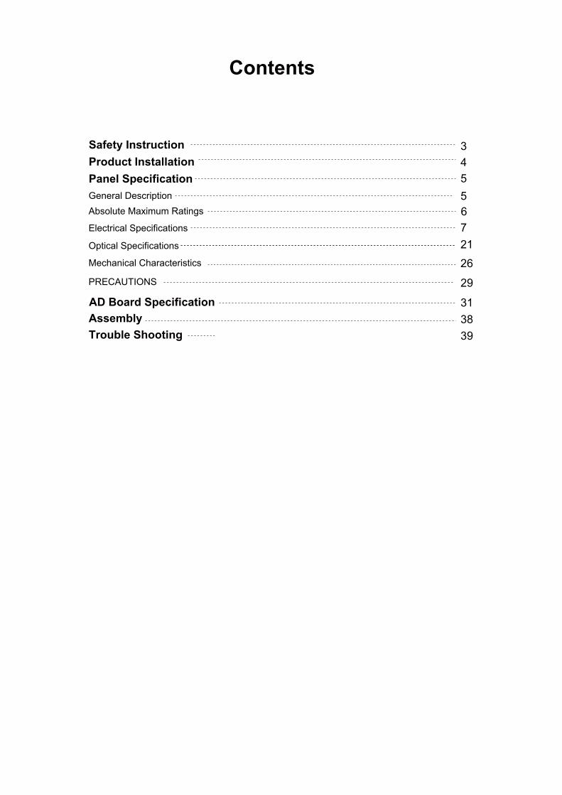
Notes: Hsync period and Hsync width-active should be even number times of tCLK. If the value is odd number times of tCLK, display control signal can be asynchronous. In order to operate this LCM a Hsync, Vsyn, and DE(data enable) signals should be used.
1. The performance of the electro-optical characteristics may be influenced by variance of the verticalrefresh rates.
2. Vsync and Hsync should be keep the above specification.3. Hsync Period, Hsync Width, and Horizontal Back Porch should be any times of of character
number(8).4. The polarity of Hsync, Vsync is not restricted.
3-3. Signal Timing Specifications
Table 6. Timing Table
This is the signal timing required at the input of the User connector. All of the interface signal timing should be satisfied with the following specifications for it’s proper operation.
ITEM SYMBOL Min Typ Max Unit Note
Period tCLK 14.28 15.625 16.00 ns
Frequency fCLK 62.5 64.0 70.0 MHz 2pixel/clk
Period tHP 852 860 906
Width-Active tWH 16 16 16
tHP
tCLK
Vertical Valid tVV 1200 1200 1200
Vertical Back Porch tVBP 24 32 42
Vertical Front Porch tVFP 4 4 4
Vertical Blank - 30 40 50
tHP
Frequency fV 59 60 61 Hz
Horizontal Back Porch tHBP 20 24 48
Horizontal Front Porch tHFP 16 20 42
Horizontal Blank - 52 60 106
Width-Active tWV 2 4 4
tCLK
Hsync
Period tVP 1230 1240 1250 tHPVsync
Horizontal Valid tHV 800 800 800Data
Enable
DCLK

Panel Specification
3-4. Signal Timing Waveforms
0.7VCC
0.3VCC
tCLK
Invalid data
Valid data
Invalid data
Invalid data
Invalid data
Pixel 0,0 Pixel 2,0
Pixel 1,0 Pixel 3,0
DE(Data Enable)
Valid data
0.5 VCC
tHP
tHBP tHV tHFP
tVP
tWV
tVBP tVV tVFP
HSync
VSync
DE(Data Enable)
DE(Data Enable)
DCLK
First data
Second data
Hsync, Vsync, DE, Data
tWH

Panel Specification
3-5. Color Data ReferenceThe Brightness of each primary color(red,green,blue) is based on the 8-bit gray scale data input for the color;the higher the binary input, the brighter the color. The table below provides a reference for color versus data input.
Table 7. COLOR DATA REFERENCE
Input Color Data
REDMSB LSB
GREENMSB LSB
BLUEMSB LSB
Black 0 0 0 0 0 0 0 0 0 0 0 0 0 0 0 0 0 0 0 0 0 0 0 0
Red (255)
Green (255)
Blue (255)
Cyan
Magenta
Yellow
White
RED (000) Dark 0 0 0 0 0 0 0 0 0 0 0 0 0 0 0 0 0 0 0 0 0 0 0 0
GREEN (000) Dark 0 0 0 0 0 0 0 0 0 0 0 0 0 0 0 0 0 0 0 0 0 0 0 0
GREEN (001) 0 0 0 0 0 0 0 0 0 0 0 0 0 0 0 1 0 0 0 0 0 0 0 0
GREEN ... ... ... ...
GREEN (254) 0 0 0 0 0 0 0 0 1 1 1 1 1 1 1 0 0 0 0 0 0 0 0 0
GREEN (255) 0 0 0 0 0 0 0 0 1 1 1 1 1 1 1 1 0 0 0 0 0 0 0 0
RED (001) 0 0 0 0 0 0 0 1 0 0 0 0 0 0 0 0 0 0 0 0 0 0 0 0
RED ... ... ... ...
RED (254) 1 1 1 1 1 1 1 0 0 0 0 0 0 0 0 0 0 0 0 0 0 0 0 0
RED (255) 1 1 1 1 1 1 1 1 0 0 0 0 0 0 0 0 0 0 0 0 0 0 0 0
BLUE (000) Dark
BLUE (001) 0 0 0 0 0 0 0 0 0 0 0 0 0 0 0 0 0 0 0 0 0 0 0 1
... ... ... ...
BLUE (254) 0 0 0 0 0 0 0 0 0 0 0 0 0 0 0 0 1 1 1 1 1 1 1 0
BLUE (255) 0 0 0 0 0 0 0 0 0 0 0 0 0 0 0 0 1 1 1 1 1 1 1 1
1 1 1 1 1 1 1 1 0 0 0 0 0 0 0 0 0 0 0 0 0 0 0 0
BasicColor
0 0 0 0 0 0 0 0 1 1 1 1 1 1 1 1 0 0 0 0 0 0 0 0
0 0 0 0 0 0 0 0 0 0 0 0 0 0 0 0 1 1 1 1 1 1 1 1
0 0 0 0 0 0 0 0 1 1 1 1 1 1 1 1 1 1 1 1 1 1 1 1
1 1 1 1 1 1 1 1 0 0 0 0 0 0 0 0 1 1 1 1 1 1 1 1
1 1 1 1 1 1 1 1 1 1 1 1 1 1 1 1 0 0 0 0 0 0 0 0
1 1 1 1 1 1 1 1 1 1 1 1 1 1 1 1 1 1 1 1 1 1 1 1
Color
R7 R6 R5 R4 R3 R2 R1 R0 G7 G6 G5 G4 G3 G2 G1 G0 B7 B6 B5 B4 B3 B2 B1 B0
0 0 0 0 0 0 0 0 0 0 0 0 0 0 0 0 0 0 0 0 0 0 0 0
BLUE

Panel Specification
3-6. Power Sequence
Notes : 1. Please avoid floating state of interface signal at invalid period.2. When the interface signal is invalid, be sure to pull down the power supply for LCD VLCD to 0V.3. Lamp power must be turn on after power supply for LCD an interface signal are valid.
ValuesParameter
Min Typ Max
T1 - - 10 ms
T2 0.01 - 50 ms
T7 400 - - ms
T3 200 - - ms
msT4 200 - -
T5 0.01 - 50 ms
Units
Table 8. POWER SEQUENCE
Interface Signal, Vi(Digital RGB signal, SCDT ,Vsync, Hsync, DE, Clock to PanelLinkTransmitter)
Power Supply for Backlight Inverter
Power Supply, VLCD
90%VLCD
90%
10% 10%
T10V
LAMP ONLAMP OFF
T3
0V
T6
LAMP OFF
T4
T2 T5 T7
Valid Data

Panel Specification
4. Optical SpecificationOptical characteristics are determined after the unit has been ‘ON’ and stable for approximately 30 minutes in a dark environment at 25±2°C. The values specified are at an approximate distance 50cm from the LCD surface at a viewing angle of Φ and θ equal to 0 °.FIG. 1 presents additional information concerning the measurement equipment and method.
LCD ModuleOptical Stage(x,y) Pritchard 880 orequivalent
50cmFIG. 1 Optical Characteristic Measurement Equipment and Method
Table 9. OPTICAL CHARACTERISTICS Ta=25 °C, VLCD=18.0V, fV=60Hz Dclk=128MHz, IBL=7mA
ValuesParameter Symbol
Min Typ MAx
Luminance Variation δ WHITE 75 - - % 3Rise TimeDecay Time
TGTG_AVR - 6 - ms 5Gray To Gray
TGTG_MAX - - 12 ms 5
Horizontal
Vertical
--
θCST_V - 178 -Viewing Angle
Horizontal θH - 178 -degree 7general
Vertical θV 178
Color CoordinatesRED
GREEN
BLUE
WHITE
RX 0.639
-0.03 +0.03
RY 0.342GX 0.295GY 0.615BX 0.146BY 0.072WX 0.313WY 0.329
θCST_H - 178 - degree
Horizontal θGMA_H - 178 -
Verticaldegree 8Effective
θGMA_V 178Gray Scale 2.2 9
TrD - 7.5 ms 4
Color shift 6
TrR - 6.5 ms 425
Response Time
Contrast Ratio CR 400 800 1Surface Luminance, white LWH 250 300 cd/m2
Units Notes
2

Panel Specification
Notes 1. Contrast Ratio(CR) is defined mathematically as :
Surface Luminance with all white pixelsContrast Ratio =
Surface Luminance with all black pixels
2. Surface luminance is luminance value at No.1 point across the LCD surface 50cmfrom the surface with all pixels displaying white. For more information see FIG 2.
3. The variation in surface luminance , δ WHITE is defined as :
Measuring point for surface luminance & measuring point for luminance variation
FIG. 2 Measure Point for Luminance
001 )%(mumixaM L( , L , .... L )
,L , .. L )Minimum(L
on91no 2no
on91no 2no ×…
=WHITEδ
1
H
A
B
V
Active AreaA : H/4 mmB : V/4 mm@ H,V : Active Area
H/10
V/10
2 3 4
7 8 9
5 6

Panel Specification
FIG. 3 Response Time
4. The response time is defined as the following figure and shall be measured by switching the input signal for “black” and “white”.Response time is the time required for the display to transition from black to white (Rise Time,TrR) and from white to black (Decay Time, TrD).
5. The Gray to Gray response time is defined as the following figure and shall be measured by switching the input signal for “Gray To Gray “.- Gray step : 5 Step - TGTG_AVR is the total average time at rising time and falling time for “Gray To Gray “.- TGTG_MAX is the max time at rising time or falling time for “Gray To Gray “.
Rising TimeGray to Gray
G255 G191 G127 G63 G0
G255
G191
G127
G63
G0
Falling Time
TrR TrD
10090
100
Optical Response

Panel Specification
6. Color shift is the angle at which the color difference is lower than 0.04.
φ = 90。(12:00)
yu
θ = 0。z
z' yd
θ
φ
φ = 180。(9:00)
A
φ = 0。(3:00) xr
φ = 270。
(6:00)
TFT LCDMODULE
xl
- Color difference (Δu’v’)
25% Box size
Viewing angle direction
- Pattern size : 25% Box size
- Viewing angle direction of color shift : Horizontal, Vertical
u’=-2x + 12y + 3
4xv’=
-2x + 12y +3
9y
Δu’v’ = (u’1-u’2)2+(v’1-v’2)2u’1, v’1 : u’v’ value at viewing angle direction
u’2, v’2 : u’v’ value at front (θ=0)
Dark skin Light skin Blue sky Foliage Blue flower Bluish greenR 98 206 85 77 129 114G 56 142 112 102 118 199B 45 123 161 46 185 178
Orange Purplish blue Moderate red Purple Yellow green Orange yellowR 219 56 211 76 160 230G 104 69 67 39 193 162B 24 174 87 86 58 29
Blue Green Red Yellow Magenta cyanR 26 72 197 241 207 35G 32 148 27 212 62 126B 145 65 37 36 151 172
White Neutral 8 Neutral 6.5 Neutral 5 Neutral 3.5 blackR 240 206 155 110 63 22G 240 206 155 110 63 22B 240 206 155 110 63 22
Average RGB values in Bruce RGB for Macbeth Chart

Panel Specification
Table 10. Gray Scale Specification
8. Effective viewing angle is the angle at which the gamma shift of gray scale is lower than 0.3.
Here the Parameter α and γ relate the signal level V to the luminance L.The GAMMA we calculate from the log-log representation (Fig. 4)
7. Viewing angle(general) is the angle at which the contrast ratio is greater than 10.
9. Gray scale specificationGamma Value is approximately 2.2. For more information see Table 10.
Gray Level Relative Luminance [%] (Typ.)
00 .12
31 1.20
63 4.57
11.3
21.4
35.2
52.8
74.4
100
95
127
159
191
223
255

Panel Specification
5. Mechanical CharacteristicsThe contents provide general mechanical characteristics. In addition the figures in the next page are detailed mechanical drawing of the LCD.
Notes : Please refer to a mechanic drawing in terms of tolerance at the next page.
Outside dimensions
Horizontal
25.0 ± 0.5 mm
Vertical
432.0 ± 0.5mm
Depth
331.5 ± 0.5mm
Bezel areaHorizontal
Vertical
Active display areaHorizontal
Vertical
408.0 mm
306.0 mm
Weight (approximate) 3,200g (Typ.) / 3250g (Max)
Surface Treatment Hard coating (3H)Anti-glare treatment of the front polarizer Haze (25%)
413.0 mm
311.0 mm

Panel Specification
6. Reliability
Environment test condition
Wave form : randomVibration level : 1.0G RMSBandwidth : 10-500HzDuration : X,Y,Z, 10 min
One time each direction
Vibration test(non-operating)5
0 - 10,000 feet(3,048m)0 - 40,000 feet(12,192m)
Altitudeoperatingstorage / shipment
7
Shock level : 100GWaveform : half sine wave, 2msDirection : ±X, ±Y, ±Z
One time each direction
Shock test(non-operating)6
Ta= 0°C 240hLow temperature operation test4
Ta= 50°C 60%RH 240hHigh temperature operation test3
Ta= -20°C 240hLow temperature storage test2
Ta= 60°C 240hHigh temperature storage test1
No Test Item Condition
Panel Specification
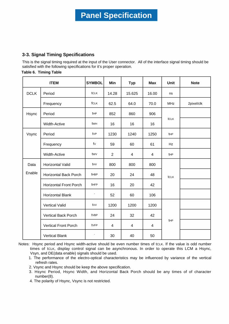
7. International Standards
7-2. EMC
a) ANSI C63.4 “Methods of Measurement of Radio-Noise Emissions from Low-Voltage Electrical and Electrical Equipment in the Range of 9kHZ to 40GHz. “American National Standards Institute(ANSI),1992b) C.I.S.P.R “Limits and Methods of Measurement of Radio Interface Characteristics of InformationTechnology Equipment.“ International Special Committee on Radio Interference.c) EN 55022 “Limits and Methods of Measurement of Radio Interface Characteristics of InformationTechnology Equipment.“ European Committee for Electrotechnical Standardization.(CENELEC), 1998( Including A1: 2000 )
7-1. Safety
a) UL 60950-1:2003, First Edition, Underwriters Laboratories, Inc.,Standard for Safety of Information Technology Equipment.b) CAN/CSA C22.2, No. 60950-1-03 1st Ed. April 1, 2003, Canadian Standards Association,Standard for Safety of Information Technology Equipment.c) EN 60950-1:2001, First Edition, European Committee for Electrotechnical Standardization(CENELEC)European Standard for Safety of Information Technology Equipment.
7-3. Environment
a) RoHS, Directive 2002/95/EC of the European Parliament and of the Council on the reduction ofthe use of certain hazardous substances in electrical and electronic equipment, January 2003.

Panel Specification
8. PRECAUTIONS
Please pay attention to the followings when you use this TFT LCD module.
8-1. MOUNTING PRECAUTIONS(1) You must mount a module using holes arranged in four corners or four sides.(2) You should consider the mounting structure so that uneven force (ex. Twisted stress) is not applied to the
module. And the case on which a module is mounted should have sufficient strength so that external force is not transmitted directly to the module.
(3) Please attach the surface transparent protective plate to the surface in order to protect the polarizer.Transparent protective plate should have sufficient strength in order to the resist external force.
(4) You should adopt radiation structure to satisfy the temperature specification.(5) Acetic acid type and chlorine type materials for the cover case are not desirable because the former
generates corrosive gas of attacking the polarizer at high temperature and the latter causes circuit break by electro-chemical reaction.
(6) Do not touch, push or rub the exposed polarizers with glass, tweezers or anything harder than HBpencil lead. And please do not rub with dust clothes with chemical treatment.Do not touch the surface of polarizer for bare hand or greasy cloth.(Some cosmetics are detrimentalto the polarizer.)
(7) When the surface becomes dusty, please wipe gently with absorbent cotton or other soft materials like chamois soaks with petroleum benzene. Normal-hexane is recommended for cleaning the adhesives used to attach front / rear polarizers. Do not use acetone, toluene and alcohol because they cause chemical damage to the polarizer.
(8) Wipe off saliva or water drops as soon as possible. Their long time contact with polarizer causes deformations and color fading.
(9) Do not open the case because inside circuits do not have sufficient strength.
8-2. OPERATING PRECAUTIONS
(1) The spike noise causes the mis-operation of circuits. It should be lower than following voltage : V=±200mV(Over and under shoot voltage)
(2) Response time depends on the temperature.(In lower temperature, it becomes longer.)(3) Brightness depends on the temperature. (In lower temperature, it becomes lower.)
And in lower temperature, response time(required time that brightness is stable after turned on) becomeslonger.
(4) Be careful for condensation at sudden temperature change. Condensation makes damage to polarizer or electrical contacted parts. And after fading condensation, smear or spot will occur.
(5) When fixed patterns are displayed for a long time, remnant image is likely to occur.(6) Module has high frequency circuits. Sufficient suppression to the electromagnetic interference shall be
done by system manufacturers. Grounding and shielding methods may be important to minimized theinterference.
(7) Please do not give any mechanical and/or acoustical impact to LCM. Otherwise, LCM can not be operated its full characteristics perfectly.
(8) A screw which is fastened up the steels should be a machine screw (if not, it causes metallic foreign material and deal LCM a fatal blow)
(9) Please do not set LCD on its edge.
Panel Specification
Since a module is composed of electronic circuits, it is not strong to electrostatic discharge. Make certain that treatment persons are connected to ground through wrist band etc. And don’t touch interface pin directly.
8-3. ELECTROSTATIC DISCHARGE CONTROL
Strong light exposure causes degradation of polarizer and color filter.
8-4. PRECAUTIONS FOR STRONG LIGHT EXPOSURE
When storing modules as spares for a long time, the following precautions are necessary.
(1) Store them in a dark place. Do not expose the module to sunlight or fluorescent light. Keep the temperature between 5°C and 35°C at normal humidity.
(2) The polarizer surface should not come in contact with any other object.It is recommended that they be stored in the container in which they were shipped.
8-5. STORAGE
8-6. HANDLING PRECAUTIONS FOR PROTECTION FILM(1) The protection film is attached to the bezel with a small masking tape.
When the protection film is peeled off, static electricity is generated between the film and polarizer.This should be peeled off slowly and carefully by people who are electrically grounded and with wellion-blown equipment or in such a condition, etc.
(2) When the module with protection film attached is stored for a long time, sometimes there remains avery small amount of glue still on the bezel after the protection film is peeled off.
(3) You can remove the glue easily. When the glue remains on the bezel surface or its vestige isrecognized, please wipe them off with absorbent cotton waste or other soft material like chamoissoaked with normal-hexane.

AD Board Specification
LCD monitor GTR24 OSD operationControl Functions
The Monitor control functions are located on the lower side of the panel.
The control key description
1. MENU : Activate the on-screen-display function
2. ∇ : Down / Brightness control
3. ∆ : Up / Brightness control
4. Auto : AUTO-ADJUSTMENT
5. : Power Switch
Description1. Menu
Press the Menu key to activate the on screen display screen. It is a toggle key. Press twice to turn off the OSD. After 30 sec. idle time, the OSD screen will automatically turn off.
2. ∇ & ∆ : Select key The two keys have two sets of functions:
When OSD screen is not activated, the two keys are
used to adjust the Backlight.
When OSD screen is activated (When "Menu" key is pressed), the two keys are used to select the wanted adjustment items
3. Auto
Press Auto Key to get the optimized quality.
4. : Power switchUse the power switch to turn ON or OFF power. We recommend turning your system power on first, then the LCD monitor.

AD Board Specification
ADJUSTING THE MONITOR
The LCD monitor is designed to work with a range of compatible video adapters on the market. Due to
the possible deviations between these video adapters, you may make some adjustment to fit the monitor
for adapter used.
ADJUSTMENT PROCEDUREFirst, you must activate the OSD screen through pressing the MENU key, the screen will show in the
center of screen as below:
OSD SCREEN
Use the ∇ & ∆ key to select the required adjustment item up or down.
Use Menu key to do the desired function or go into the second menu item to do the further
change.
Use the ∇ & ∆ key to select the Exit item to turn off OSD. Or After 30 sec. idle time, the
OSD screen will automatically turn off.
the Exit item to

AD Board Specification
AUTO-ADJUSTMENT
WE STRONGLY RECOMMEND THAT YOU USE THIS ITEM TO GET THE OPTIMIZED VISUAL QUALITY.
Use the ∇ & ∆ key to select auto-adjustment, and then press Menu Key to get the optimized
quality.
Or press Auto Key to get the optimized directly.
BRIGHTNESS ADJUSTMENT Use the ∇ & ∆ key to select the Brightness item, press Menu Key to change the
brightness value.
Use the ∇ & ∆ key to adjust the Brightness.
Then press menu key to confirm.
ADJUST THE CONTRAST VALUE
Use the ∇ & ∆ key to select the CONTRAST item, then press Menu Key to get the best
contrast optimization.
Use the ∇ & ∆ key to adjust contrast value.
Screen Settings Use the ∇ & ∆ key to select the Screen Settings item, then press Menu Key to get the
he Brightness item
CONTRAST item
ings item, th

AD Board Specification
best Screen Settings optimization.
H.Position Use the ∇ & ∆ key to select the H.Position item, then press Menu Key to get the best
optimization.
Use the ∇ & ∆ key to adjust H.Position value.
Then press menu key to confirm.
V.Position Use the ∇ & ∆ key to select the V.Position item, then press Menu Key to get the best
optimization.
Use the ∇ & ∆ key to adjust V.Position value.
Then press menu key to confirm.
Clock Use the ∇ & ∆ key to select the Clock item, then press Menu Key to get the best
optimization.
Use the ∇ & ∆ key to adjust increase or decrease video H Size of the picture.
Then press menu key to confirm.

AD Board Specification
Phase Use the ∇ & ∆ key to select the Phase item, then press Menu Key to get the best
optimization.
Use the ∇ & ∆ key to adjust increase or decrease video Quality of the picture.
Then press menu key to confirm.
Color Temperture Use the ∇ & ∆ key to select the Color Temp item, then press Menu Key to get the
language selection.
Use the ∇ & ∆ key to select the adjust the display color of the picture.
Use the ∇ & ∆ key to select temperature 9300K, 7500K and 6500K of the picture.
User Color Use the ∇ & ∆ key to select User Color, then press Menu Key to get the best color
optimization.
Use the ∇ & ∆ key to select Red, Green & Blue to adjust the display user color of the picture.
Color Temp item

AD Board Specification
Auto Gain Use the ∇ & ∆ key to select Auto Gain, then press Menu Key to get the best color
optimization that will be activated the auto adjusting input video color level for the picture.
sRGB Use the ∇ & ∆ key to select SRGB, then press Menu Key to get the best color optimization.
Language Setting Use the ∇ & ∆ key to select the Language item, then press Menu Key to get the
language selection.
Use the ∇ & ∆ key to select the Language.
Then press Menu key to confirm.
age item,

AD Board Specification
OSD Setting Use the ∇ & ∆ key to select the OSD Setting item, then press Menu Key to get the
OSD setting selection.
You could set up the property of Position, Display Timer, and Transparency of OSD menu.
Volume Use the ∇ & ∆ key to select the Volume item, then press Menu Key to get the Volume
setting.
Use the ∇ & ∆ key to select Volume and mute on/off.
Use menu key to select Mute on / off
Then select Exit to the last page.
Recall Use the ∇ & ∆ key to select the Recall item, then press Menu Key to get the default
setting.
item, t
key to select the Volume item,
the Recall item


17
Trouble Shooting
If your monitor fails to operate correctly, consult the following chart for possible solution before calling for repairs/RMA.
Condition Possible Solution
The screen is not synchronized? 1. Check if the signal cable is firmly seated in the socket.
2. Check if the output level matches the input level of your computer.
3. Make sure the signal timings of the computer system are within the specification of the monitor.
4. If your computer was working with a CRT monitor, you should check the current signal timing and turn off your computer before you connect the VGA Cable to this monitor.
The Picture does not appear? 5. Make sure the power cord is plugged into the power outlet and into the back of the monitor.
6. Check if the signal cable is firmly seated in the socket.
7. Check if the Power is ON at the computer
8. Check if the brightness control is at the appropriate position, not at the minimum.
The position of the screen is not in the center?
9. Press the Auto button. Adjust the image position using the Horizontal Position and/or Vertical Position in OSD Main Controls.
The screen is too bright/dark. 10. Check if the brightness or contrast control is at the appropriate position, not at the Maximum/Minimum.


![manua del[1]](https://img.pdfslide.net/doc/110x75/5571f24149795947648c651d/manua-del1.jpg)